EP0803901A2 - Montageverfahren für eine Mehrzahl von Halbleiteranordnungen in korrespondierenden Trägern - Google Patents
Montageverfahren für eine Mehrzahl von Halbleiteranordnungen in korrespondierenden Trägern Download PDFInfo
- Publication number
- EP0803901A2 EP0803901A2 EP97106644A EP97106644A EP0803901A2 EP 0803901 A2 EP0803901 A2 EP 0803901A2 EP 97106644 A EP97106644 A EP 97106644A EP 97106644 A EP97106644 A EP 97106644A EP 0803901 A2 EP0803901 A2 EP 0803901A2
- Authority
- EP
- European Patent Office
- Prior art keywords
- semiconductor
- substrate
- adhesive layer
- supporter
- module
- Prior art date
- Legal status (The legal status is an assumption and is not a legal conclusion. Google has not performed a legal analysis and makes no representation as to the accuracy of the status listed.)
- Granted
Links
Images


Classifications
-
- H—ELECTRICITY
- H10—SEMICONDUCTOR DEVICES; ELECTRIC SOLID-STATE DEVICES NOT OTHERWISE PROVIDED FOR
- H10P—GENERIC PROCESSES OR APPARATUS FOR THE MANUFACTURE OR TREATMENT OF DEVICES COVERED BY CLASS H10
- H10P72/00—Handling or holding of wafers, substrates or devices during manufacture or treatment thereof
- H10P72/70—Handling or holding of wafers, substrates or devices during manufacture or treatment thereof for supporting or gripping
- H10P72/74—Handling or holding of wafers, substrates or devices during manufacture or treatment thereof for supporting or gripping using temporarily an auxiliary support
-
- G—PHYSICS
- G06—COMPUTING OR CALCULATING; COUNTING
- G06K—GRAPHICAL DATA READING; PRESENTATION OF DATA; RECORD CARRIERS; HANDLING RECORD CARRIERS
- G06K19/00—Record carriers for use with machines and with at least a part designed to carry digital markings
- G06K19/06—Record carriers for use with machines and with at least a part designed to carry digital markings characterised by the kind of the digital marking, e.g. shape, nature, code
- G06K19/067—Record carriers with conductive marks, printed circuits or semiconductor circuit elements, e.g. credit or identity cards also with resonating or responding marks without active components
- G06K19/07—Record carriers with conductive marks, printed circuits or semiconductor circuit elements, e.g. credit or identity cards also with resonating or responding marks without active components with integrated circuit chips
- G06K19/077—Constructional details, e.g. mounting of circuits in the carrier
- G06K19/07745—Mounting details of integrated circuit chips
-
- H—ELECTRICITY
- H10—SEMICONDUCTOR DEVICES; ELECTRIC SOLID-STATE DEVICES NOT OTHERWISE PROVIDED FOR
- H10W—GENERIC PACKAGES, INTERCONNECTIONS, CONNECTORS OR OTHER CONSTRUCTIONAL DETAILS OF DEVICES COVERED BY CLASS H10
- H10W42/00—Arrangements for protection of devices
- H10W42/121—Arrangements for protection of devices protecting against mechanical damage
-
- H—ELECTRICITY
- H10—SEMICONDUCTOR DEVICES; ELECTRIC SOLID-STATE DEVICES NOT OTHERWISE PROVIDED FOR
- H10W—GENERIC PACKAGES, INTERCONNECTIONS, CONNECTORS OR OTHER CONSTRUCTIONAL DETAILS OF DEVICES COVERED BY CLASS H10
- H10W74/00—Encapsulations, e.g. protective coatings
- H10W74/10—Encapsulations, e.g. protective coatings characterised by their shape or disposition
- H10W74/111—Encapsulations, e.g. protective coatings characterised by their shape or disposition the semiconductor body being completely enclosed
- H10W74/114—Encapsulations, e.g. protective coatings characterised by their shape or disposition the semiconductor body being completely enclosed by a substrate and the encapsulations
-
- H—ELECTRICITY
- H10—SEMICONDUCTOR DEVICES; ELECTRIC SOLID-STATE DEVICES NOT OTHERWISE PROVIDED FOR
- H10W—GENERIC PACKAGES, INTERCONNECTIONS, CONNECTORS OR OTHER CONSTRUCTIONAL DETAILS OF DEVICES COVERED BY CLASS H10
- H10W72/00—Interconnections or connectors in packages
- H10W72/50—Bond wires
- H10W72/551—Materials of bond wires
- H10W72/552—Materials of bond wires comprising metals or metalloids, e.g. silver
- H10W72/5522—Materials of bond wires comprising metals or metalloids, e.g. silver comprising gold [Au]
-
- H—ELECTRICITY
- H10—SEMICONDUCTOR DEVICES; ELECTRIC SOLID-STATE DEVICES NOT OTHERWISE PROVIDED FOR
- H10W—GENERIC PACKAGES, INTERCONNECTIONS, CONNECTORS OR OTHER CONSTRUCTIONAL DETAILS OF DEVICES COVERED BY CLASS H10
- H10W74/00—Encapsulations, e.g. protective coatings
-
- H—ELECTRICITY
- H10—SEMICONDUCTOR DEVICES; ELECTRIC SOLID-STATE DEVICES NOT OTHERWISE PROVIDED FOR
- H10W—GENERIC PACKAGES, INTERCONNECTIONS, CONNECTORS OR OTHER CONSTRUCTIONAL DETAILS OF DEVICES COVERED BY CLASS H10
- H10W90/00—Package configurations
- H10W90/701—Package configurations characterised by the relative positions of pads or connectors relative to package parts
- H10W90/751—Package configurations characterised by the relative positions of pads or connectors relative to package parts of bond wires
- H10W90/754—Package configurations characterised by the relative positions of pads or connectors relative to package parts of bond wires between a chip and a stacked insulating package substrate, interposer or RDL
Definitions
- This invention relates to a manufacturing method for a semiconductor device, and more particularly to a method of bonding a plurality of semiconductor module and a substrate supporting it in a corresponding plurality of supporters.
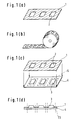
- a semiconductor chip 25 is bonded on the surface of a substrate 13, and a bonding pad 29 of the semiconductor chip 25 is connected by a gold wire 27 to a terminal formed on the substrate 13 to be connected to the semiconductor chip.
- the semiconductor chip may be connected to the chip connecting terminal on the substrate by a flip-chip bonding technique using a bump.
- the semiconductor chip 25 is then sealed by a molding portion 14.
- a non-volatile semiconductor memory such as a flash EEPROM, is used as the semiconductor chip 25.
- the periphery of the substrate 13 is exposed to the outside and surrounds the resin mold section 14.
- the opposite surface of the substrate is provided with a plain connection terminal 12 which can be connected to external circuits. Commonly, the external connection terminal 12 is connected to the chip connecting terminal 26 by a through hole 28.
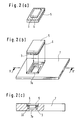
- the adhesive sheet 1 When the adhesive sheet 1 is applied to the substrate 4 having a plurality of the semiconductor modules, the adhesive sheet 1 may be applied simultaneously on the entire surface of the substrate 4. Alternatively, the adhesive sheet 1 may be sequentially applied to each module portion 3.
- Fig. 2(c) shows a cross-sectional view of the devices shown in Fig. 2(b) taken along a line X-X .
- the semiconductor module 5 applied with the adhesive piece 6 on its periphery is bonded to the concave portion 7a of the module supporter 7.
- the bending stress exerted on the module supporter 7 is not forced upon a semiconductor chip 25 contained in the molding portion 3, because the size of the molding 3 is smaller than that of the concave portion 7a.
- a gap 33 created between the molding portion 3 and the bottom of the concave portion 7a substantially blocks any pressure applied to the molding portion 3.
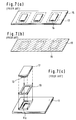
- the second embodiment is intended to simultaneously bond an adhesive sheet to a plurality of semiconductor sheets.
- the opening portions 2 and the molding portions 3 can be properly aligned and may require only one bonding process.
- the entire bonding portion of the semiconductor module can be applied with the adhesive. Accordingly, adhesive strength is increased, and the mechanical strength of an IC card using the semiconductor device formed in such a manner is improved, thus improving reliability of the device.
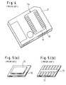
- the above-mentioned process according to the present invention may be used with semiconductor modules having external connection terminals 12 on the opposite surface of the molding surface, as shown in Fig. 5(b).
- the semiconductor module constructed using the present invention is preferably mounted in a module supporter 11 formed of resin having, for example, a length, a width, and a thickness of 37 mm x 45 mm x 0.76 mm, respectively.
- the card-type module is connected to an adapter card (not shown).
- the adapter card may be configured to be used with a PCMCIA card slot or the like.
- the adapter card includes an insertion hole for receiving a card-type module therein, and a standard connector for attaching to, for example, a PCMCIA card slot of a personal computer.
- the adapter card has an interior provided with a connector for being contacted with the external-connection terminal of the card-type module and an interface circuit for functioning as an interface between the card-type module and an external apparatus, such as a personal computer.
- the adapter card may be of types other than a PCMCIA card.
- a connector may be provided, together with the interface circuit, in the main body of a personal computer or a camera to communicate with the external-connection terminal of the card-type module.
Landscapes
- Engineering & Computer Science (AREA)
- Computer Hardware Design (AREA)
- Microelectronics & Electronic Packaging (AREA)
- Physics & Mathematics (AREA)
- General Physics & Mathematics (AREA)
- Theoretical Computer Science (AREA)
- Credit Cards Or The Like (AREA)
- Die Bonding (AREA)
- Structures Or Materials For Encapsulating Or Coating Semiconductor Devices Or Solid State Devices (AREA)
- Dicing (AREA)
Applications Claiming Priority (3)
| Application Number | Priority Date | Filing Date | Title |
|---|---|---|---|
| JP10535996 | 1996-04-25 | ||
| JP10535996 | 1996-04-25 | ||
| JP105359/96 | 1996-04-25 |
Publications (3)
| Publication Number | Publication Date |
|---|---|
| EP0803901A2 true EP0803901A2 (de) | 1997-10-29 |
| EP0803901A3 EP0803901A3 (de) | 1999-09-22 |
| EP0803901B1 EP0803901B1 (de) | 2006-08-16 |
Family
ID=14405537
Family Applications (1)
| Application Number | Title | Priority Date | Filing Date |
|---|---|---|---|
| EP97106644A Expired - Lifetime EP0803901B1 (de) | 1996-04-25 | 1997-04-22 | Montageverfahren für eine Mehrzahl von Halbleiteranordnungen in korrespondierenden Trägern |
Country Status (6)
| Country | Link |
|---|---|
| US (1) | US5956601A (de) |
| EP (1) | EP0803901B1 (de) |
| KR (1) | KR100269850B1 (de) |
| CN (1) | CN1092399C (de) |
| DE (1) | DE69736499T2 (de) |
| TW (1) | TW334619B (de) |
Cited By (1)
| Publication number | Priority date | Publication date | Assignee | Title |
|---|---|---|---|---|
| WO2001095486A1 (en) * | 2000-06-06 | 2001-12-13 | Sawtek Inc. | System and method for array processing of surface acoustic wave devices |
Families Citing this family (14)
| Publication number | Priority date | Publication date | Assignee | Title |
|---|---|---|---|---|
| FR2773900B1 (fr) * | 1998-01-22 | 2000-02-18 | Gemplus Card Int | Carte a circuit(s) integre(s) a contact, comportant une minicarte detachable |
| SG80077A1 (en) * | 1998-10-19 | 2001-04-17 | Sony Corp | Semiconductor integrated circuit card manufacturing method, and semiconductor integrated circuit card |
| JP2002092575A (ja) * | 2000-09-19 | 2002-03-29 | Mitsubishi Electric Corp | 小型カードとその製造方法 |
| JP4162930B2 (ja) * | 2002-06-25 | 2008-10-08 | 富士機械製造株式会社 | 電子部品実装装置における基板搬送装置 |
| JP4002143B2 (ja) * | 2002-07-10 | 2007-10-31 | 株式会社ルネサステクノロジ | 半導体装置の製造方法 |
| CN100336072C (zh) * | 2004-06-16 | 2007-09-05 | 台湾典范半导体股份有限公司 | 记忆卡的构装方法及其结构 |
| USD794641S1 (en) * | 2009-01-07 | 2017-08-15 | Samsung Electronics Co., Ltd. | Memory device |
| USD795262S1 (en) * | 2009-01-07 | 2017-08-22 | Samsung Electronics Co., Ltd. | Memory device |
| USD795261S1 (en) * | 2009-01-07 | 2017-08-22 | Samsung Electronics Co., Ltd. | Memory device |
| USD794034S1 (en) * | 2009-01-07 | 2017-08-08 | Samsung Electronics Co., Ltd. | Memory device |
| USD794642S1 (en) * | 2009-01-07 | 2017-08-15 | Samsung Electronics Co., Ltd. | Memory device |
| USD794643S1 (en) * | 2009-01-07 | 2017-08-15 | Samsung Electronics Co., Ltd. | Memory device |
| USD794644S1 (en) * | 2009-01-07 | 2017-08-15 | Samsung Electronics Co., Ltd. | Memory device |
| CN111640677B (zh) * | 2020-03-02 | 2022-04-26 | 浙江集迈科微电子有限公司 | 一种凹槽内芯片放置方法 |
Family Cites Families (36)
| Publication number | Priority date | Publication date | Assignee | Title |
|---|---|---|---|---|
| FR2439478A1 (fr) * | 1978-10-19 | 1980-05-16 | Cii Honeywell Bull | Boitier plat pour dispositifs a circuits integres |
| JPS5623759A (en) * | 1979-08-01 | 1981-03-06 | Hitachi Ltd | Resin-sealed semiconductor device and manufacture thereof |
| JP2582013B2 (ja) * | 1991-02-08 | 1997-02-19 | 株式会社東芝 | 樹脂封止型半導体装置及びその製造方法 |
| IT1212711B (it) * | 1983-03-09 | 1989-11-30 | Ates Componenti Elettron | Dispositivo a semiconduttore aforma di scheda piana con contatti elettrici su ambedue le facce eprocedimento per la sua fabbricazione. |
| FR2580416B1 (fr) * | 1985-04-12 | 1987-06-05 | Radiotechnique Compelec | Procede et dispositif pour fabriquer une carte d'identification electronique |
| DE3546780C2 (de) * | 1985-09-02 | 1996-04-25 | Amphenol Corp | Kontaktiereinrichtung für eine Chipkarte |
| JPS6478397A (en) * | 1987-09-18 | 1989-03-23 | Mitsubishi Electric Corp | Ic card writing system |
| FR2624635B1 (fr) * | 1987-12-14 | 1991-05-10 | Sgs Thomson Microelectronics | Support de composant electronique pour carte memoire et produit ainsi obtenu |
| JP2510694B2 (ja) * | 1988-09-16 | 1996-06-26 | 大日本印刷株式会社 | Icカ―ド |
| US5068714A (en) * | 1989-04-05 | 1991-11-26 | Robert Bosch Gmbh | Method of electrically and mechanically connecting a semiconductor to a substrate using an electrically conductive tacky adhesive and the device so made |
| US5535328A (en) * | 1989-04-13 | 1996-07-09 | Sandisk Corporation | Non-volatile memory system card with flash erasable sectors of EEprom cells including a mechanism for substituting defective cells |
| DE69024086T2 (de) * | 1989-04-13 | 1996-06-20 | Sundisk Corp | EEprom-System mit Blocklöschung |
| JPH02301155A (ja) * | 1989-05-16 | 1990-12-13 | Citizen Watch Co Ltd | Icモジュールの固定方法 |
| FR2659157B2 (fr) * | 1989-05-26 | 1994-09-30 | Lemaire Gerard | Procede de fabrication d'une carte dite carte a puce, et carte obtenue par ce procede. |
| US5200362A (en) * | 1989-09-06 | 1993-04-06 | Motorola, Inc. | Method of attaching conductive traces to an encapsulated semiconductor die using a removable transfer film |
| CA2027823C (en) * | 1989-10-31 | 1994-11-08 | Tomoshige Oka | Ic card having an integrated circuit module and air discharge opening |
| US5153818A (en) * | 1990-04-20 | 1992-10-06 | Rohm Co., Ltd. | Ic memory card with an anisotropic conductive rubber interconnector |
| JP2874279B2 (ja) * | 1990-05-10 | 1999-03-24 | 三菱電機株式会社 | 薄型半導体装置の製造方法 |
| JPH0416396A (ja) * | 1990-05-10 | 1992-01-21 | Mitsubishi Electric Corp | 半導体装置カード |
| JP2560895B2 (ja) * | 1990-07-25 | 1996-12-04 | 三菱電機株式会社 | Icカードの製造方法およびicカード |
| FR2673017A1 (fr) * | 1991-02-18 | 1992-08-21 | Schlumberger Ind Sa | Procede de fabrication d'un module electronique pour carte a memoire et module electronique ainsi obtenu. |
| US5663901A (en) * | 1991-04-11 | 1997-09-02 | Sandisk Corporation | Computer memory cards using flash EEPROM integrated circuit chips and memory-controller systems |
| US5284784A (en) * | 1991-10-02 | 1994-02-08 | National Semiconductor Corporation | Buried bit-line source-side injection flash memory cell |
| US5299089A (en) * | 1991-10-28 | 1994-03-29 | E. I. Dupont De Nemours & Co. | Connector device having two storage decks and three contact arrays for one hard disk drive package or two memory cards |
| FR2686172B1 (fr) * | 1992-01-14 | 1996-09-06 | Gemplus Card Int | Carte enfichable pour microordinateur formant lecteur de carte a contacts affleurants. |
| US5169056A (en) * | 1992-02-21 | 1992-12-08 | Eastman Kodak Company | Connecting of semiconductor chips to circuit substrates |
| US5247423A (en) * | 1992-05-26 | 1993-09-21 | Motorola, Inc. | Stacking three dimensional leadless multi-chip module and method for making the same |
| JP2674924B2 (ja) * | 1992-07-13 | 1997-11-12 | 積水化学工業株式会社 | Icカード製造装置及びそれに供される接着片の供給ロールの製造方法 |
| US5469399A (en) * | 1993-03-16 | 1995-11-21 | Kabushiki Kaisha Toshiba | Semiconductor memory, memory card, and method of driving power supply for EEPROM |
| JPH0737049A (ja) * | 1993-07-23 | 1995-02-07 | Toshiba Corp | 外部記憶装置 |
| TW272311B (de) * | 1994-01-12 | 1996-03-11 | At & T Corp | |
| US5480842A (en) * | 1994-04-11 | 1996-01-02 | At&T Corp. | Method for fabricating thin, strong, and flexible die for smart cards |
| KR0144818B1 (ko) * | 1994-07-25 | 1998-08-17 | 김광호 | 낸드형 플래쉬메모리 아이씨카드 |
| US5508971A (en) * | 1994-10-17 | 1996-04-16 | Sandisk Corporation | Programmable power generation circuit for flash EEPROM memory systems |
| KR0152042B1 (ko) * | 1995-04-15 | 1998-10-15 | 김광호 | 낸드형 플래쉬메모리 아이씨카드 기록장치 |
| US5596532A (en) * | 1995-10-18 | 1997-01-21 | Sandisk Corporation | Flash EEPROM self-adaptive voltage generation circuit operative within a continuous voltage source range |
-
1997
- 1997-04-17 US US08/839,358 patent/US5956601A/en not_active Expired - Lifetime
- 1997-04-21 TW TW086105149A patent/TW334619B/zh not_active IP Right Cessation
- 1997-04-22 EP EP97106644A patent/EP0803901B1/de not_active Expired - Lifetime
- 1997-04-22 DE DE69736499T patent/DE69736499T2/de not_active Expired - Lifetime
- 1997-04-23 KR KR1019970015183A patent/KR100269850B1/ko not_active Expired - Fee Related
- 1997-04-24 CN CN97110389A patent/CN1092399C/zh not_active Expired - Fee Related
Cited By (2)
| Publication number | Priority date | Publication date | Assignee | Title |
|---|---|---|---|---|
| WO2001095486A1 (en) * | 2000-06-06 | 2001-12-13 | Sawtek Inc. | System and method for array processing of surface acoustic wave devices |
| US6928718B2 (en) | 2000-06-06 | 2005-08-16 | Sawtekk, Inc. | Method for array processing of surface acoustic wave devices |
Also Published As
| Publication number | Publication date |
|---|---|
| DE69736499D1 (de) | 2006-09-28 |
| KR100269850B1 (ko) | 2000-10-16 |
| DE69736499T2 (de) | 2007-08-16 |
| CN1092399C (zh) | 2002-10-09 |
| EP0803901B1 (de) | 2006-08-16 |
| TW334619B (en) | 1998-06-21 |
| US5956601A (en) | 1999-09-21 |
| EP0803901A3 (de) | 1999-09-22 |
| CN1173041A (zh) | 1998-02-11 |
Similar Documents
| Publication | Publication Date | Title |
|---|---|---|
| EP0803901B1 (de) | Montageverfahren für eine Mehrzahl von Halbleiteranordnungen in korrespondierenden Trägern | |
| US7094633B2 (en) | Method for efficiently producing removable peripheral cards | |
| US5600175A (en) | Apparatus and method for flat circuit assembly | |
| US6462273B1 (en) | Semiconductor card and method of fabrication | |
| US4549247A (en) | Carrier element for IC-modules | |
| JP2849594B2 (ja) | 電子モジュールの封止方法 | |
| EP1639644B1 (de) | Kapselung für integrierte Schaltungen mit gestapelten integrierten Schaltungen und Verfahren dafür | |
| KR100280170B1 (ko) | 반도체장치용 기판과 그 제조방법, 반도체장치, 카드형 모듈 및 정보기억장치 | |
| EP0435093A2 (de) | Dünne vergossene oberflächenmontierbare elektronische Anordnung | |
| US20030029920A1 (en) | Molded memory module and method of making the module absent a substrate support | |
| US6025997A (en) | Chip module for semiconductor chips having arbitrary footprints | |
| CN103026371B (zh) | 芯片电子器件和通过卷绕进行制造的方法 | |
| CN1305618A (zh) | 制造集成电路卡的方法和按照这种方法制造的卡 | |
| US20010001507A1 (en) | Substrate for a semiconductor device, a semiconductor device, a card type module, and a data memory device | |
| JP2001177005A (ja) | 半導体装置及びその製造方法 | |
| JPH0789280A (ja) | Icモジュール | |
| JP3485736B2 (ja) | 半導体装置とその製造方法 | |
| JP3976984B2 (ja) | 半導体装置及びその製造方法 | |
| JPH1056028A (ja) | 半導体装置の製造方法 | |
| KR20050069941A (ko) | 소형 카드의 제조 방법 및, 카드형 반도체 기억 장치의제조 방법 | |
| JP2010251764A (ja) | パッケージ材料と基板との間の接着力を高める封止方法 | |
| JPH118348A (ja) | 複数のicチップを備えた半導体装置の構造 | |
| JPS63317395A (ja) | Icカ−ド | |
| JPS60129897A (ja) | 小型電子機器 | |
| JPH11301153A (ja) | Icモジュールとそれを使用したicカード |
Legal Events
| Date | Code | Title | Description |
|---|---|---|---|
| PUAI | Public reference made under article 153(3) epc to a published international application that has entered the european phase |
Free format text: ORIGINAL CODE: 0009012 |
|
| 17P | Request for examination filed |
Effective date: 19970422 |
|
| AK | Designated contracting states |
Kind code of ref document: A2 Designated state(s): DE FR GB |
|
| PUAL | Search report despatched |
Free format text: ORIGINAL CODE: 0009013 |
|
| AK | Designated contracting states |
Kind code of ref document: A3 Designated state(s): DE FR GB |
|
| GRAP | Despatch of communication of intention to grant a patent |
Free format text: ORIGINAL CODE: EPIDOSNIGR1 |
|
| GRAS | Grant fee paid |
Free format text: ORIGINAL CODE: EPIDOSNIGR3 |
|
| GRAA | (expected) grant |
Free format text: ORIGINAL CODE: 0009210 |
|
| AK | Designated contracting states |
Kind code of ref document: B1 Designated state(s): DE FR GB |
|
| REG | Reference to a national code |
Ref country code: GB Ref legal event code: FG4D |
|
| REF | Corresponds to: |
Ref document number: 69736499 Country of ref document: DE Date of ref document: 20060928 Kind code of ref document: P |
|
| ET | Fr: translation filed | ||
| PLBE | No opposition filed within time limit |
Free format text: ORIGINAL CODE: 0009261 |
|
| STAA | Information on the status of an ep patent application or granted ep patent |
Free format text: STATUS: NO OPPOSITION FILED WITHIN TIME LIMIT |
|
| 26N | No opposition filed |
Effective date: 20070518 |
|
| PGFP | Annual fee paid to national office [announced via postgrant information from national office to epo] |
Ref country code: DE Payment date: 20120425 Year of fee payment: 16 |
|
| PGFP | Annual fee paid to national office [announced via postgrant information from national office to epo] |
Ref country code: FR Payment date: 20120504 Year of fee payment: 16 Ref country code: GB Payment date: 20120418 Year of fee payment: 16 |
|
| GBPC | Gb: european patent ceased through non-payment of renewal fee |
Effective date: 20130422 |
|
| PG25 | Lapsed in a contracting state [announced via postgrant information from national office to epo] |
Ref country code: GB Free format text: LAPSE BECAUSE OF NON-PAYMENT OF DUE FEES Effective date: 20130422 Ref country code: DE Free format text: LAPSE BECAUSE OF NON-PAYMENT OF DUE FEES Effective date: 20131101 |
|
| REG | Reference to a national code |
Ref country code: FR Ref legal event code: ST Effective date: 20131231 |
|
| REG | Reference to a national code |
Ref country code: DE Ref legal event code: R119 Ref document number: 69736499 Country of ref document: DE Effective date: 20131101 |
|
| PG25 | Lapsed in a contracting state [announced via postgrant information from national office to epo] |
Ref country code: FR Free format text: LAPSE BECAUSE OF NON-PAYMENT OF DUE FEES Effective date: 20130430 |