EP0802702A2 - Energielieferung durch Fluores zenzlampe mit kalter Kathode und hoher Wirksamkeit - Google Patents
Energielieferung durch Fluores zenzlampe mit kalter Kathode und hoher Wirksamkeit Download PDFInfo
- Publication number
- EP0802702A2 EP0802702A2 EP97105722A EP97105722A EP0802702A2 EP 0802702 A2 EP0802702 A2 EP 0802702A2 EP 97105722 A EP97105722 A EP 97105722A EP 97105722 A EP97105722 A EP 97105722A EP 0802702 A2 EP0802702 A2 EP 0802702A2
- Authority
- EP
- European Patent Office
- Prior art keywords
- semiconductor switch
- power supply
- switched
- transformer
- mode power
- Prior art date
- Legal status (The legal status is an assumption and is not a legal conclusion. Google has not performed a legal analysis and makes no representation as to the accuracy of the status listed.)
- Granted
Links
Images

Classifications
-
- H—ELECTRICITY
- H02—GENERATION; CONVERSION OR DISTRIBUTION OF ELECTRIC POWER
- H02M—APPARATUS FOR CONVERSION BETWEEN AC AND AC, BETWEEN AC AND DC, OR BETWEEN DC AND DC, AND FOR USE WITH MAINS OR SIMILAR POWER SUPPLY SYSTEMS; CONVERSION OF DC OR AC INPUT POWER INTO SURGE OUTPUT POWER; CONTROL OR REGULATION THEREOF
- H02M3/00—Conversion of DC power input into DC power output
- H02M3/22—Conversion of DC power input into DC power output with intermediate conversion into AC
- H02M3/24—Conversion of DC power input into DC power output with intermediate conversion into AC by static converters
- H02M3/28—Conversion of DC power input into DC power output with intermediate conversion into AC by static converters using discharge tubes with control electrode or semiconductor devices with control electrode to produce the intermediate AC
- H02M3/325—Conversion of DC power input into DC power output with intermediate conversion into AC by static converters using discharge tubes with control electrode or semiconductor devices with control electrode to produce the intermediate AC using devices of a triode or a transistor type requiring continuous application of a control signal
- H02M3/335—Conversion of DC power input into DC power output with intermediate conversion into AC by static converters using discharge tubes with control electrode or semiconductor devices with control electrode to produce the intermediate AC using devices of a triode or a transistor type requiring continuous application of a control signal using semiconductor devices only
- H02M3/33569—Conversion of DC power input into DC power output with intermediate conversion into AC by static converters using discharge tubes with control electrode or semiconductor devices with control electrode to produce the intermediate AC using devices of a triode or a transistor type requiring continuous application of a control signal using semiconductor devices only having several active switching elements
- H02M3/33571—Half-bridge at primary side of an isolation transformer
-
- H—ELECTRICITY
- H02—GENERATION; CONVERSION OR DISTRIBUTION OF ELECTRIC POWER
- H02M—APPARATUS FOR CONVERSION BETWEEN AC AND AC, BETWEEN AC AND DC, OR BETWEEN DC AND DC, AND FOR USE WITH MAINS OR SIMILAR POWER SUPPLY SYSTEMS; CONVERSION OF DC OR AC INPUT POWER INTO SURGE OUTPUT POWER; CONTROL OR REGULATION THEREOF
- H02M3/00—Conversion of DC power input into DC power output
- H02M3/01—Resonant DC/DC converters
-
- Y—GENERAL TAGGING OF NEW TECHNOLOGICAL DEVELOPMENTS; GENERAL TAGGING OF CROSS-SECTIONAL TECHNOLOGIES SPANNING OVER SEVERAL SECTIONS OF THE IPC; TECHNICAL SUBJECTS COVERED BY FORMER USPC CROSS-REFERENCE ART COLLECTIONS [XRACs] AND DIGESTS
- Y02—TECHNOLOGIES OR APPLICATIONS FOR MITIGATION OR ADAPTATION AGAINST CLIMATE CHANGE
- Y02B—CLIMATE CHANGE MITIGATION TECHNOLOGIES RELATED TO BUILDINGS, e.g. HOUSING, HOUSE APPLIANCES OR RELATED END-USER APPLICATIONS
- Y02B70/00—Technologies for an efficient end-user side electric power management and consumption
- Y02B70/10—Technologies improving the efficiency by using switched-mode power supplies [SMPS], i.e. efficient power electronics conversion e.g. power factor correction or reduction of losses in power supplies or efficient standby modes
Definitions
- the present invention relates generally to power supplies for a cold-cathode fluorescent lamp (“CCFL”) that may be used for back lighting a display of a portable device, and, more particularly, to a switched-mode inverter circuit which uses a capacitor to reset a transformer's core, and uses its magnetizing inductance to store and transfer energy during negative half-cycles.
- CCFL cold-cathode fluorescent lamp
- CCFLs are high-efficiency, long-life light sources.
- incandescent lamps have efficiency in the range of 15 to 25 lumens per watt, while both FLs and CCFLs have efficiency in the range of 40 to 60 lumens per watt.
- the average life of an incandescent lamp is only about 1,000 hours. However, FLs and CCFLs, on average, last for 10,000 hours or more.
- CCFL omits filaments that are included in a FL. Due to their simpler mechanical construction and high efficiency, miniature CCFLs are generally used as a source of back lighting for Liquid Crystal Displays ("LCDs"). LCDs, whether color or monochrome, are widely used as displays in portable computers and televisions, and in instrument panels of airplanes and automobiles.
- LCDs Liquid Crystal Displays
- ac alternating current
- Typical starting voltage is around 1,000 volts AC (“Vac”), and typical operating voltage is about 600 Vac.
- a dc power source such as a rechargeable battery, portable computers and televisions, and instrument panels, include a dc-to-ac inverter having a step-up transformer.
- a Royer circuit may include two NPN bipolar transistors 12 and 14 together with a saturable-core transformer 16. Collectors 18 of each of the transistors 12 and 14 connect respectively to opposite ends of a primary winding 22 of the transformer 16. A center-tap 24 of the transformer 16 connects to a positive terminal 26 of a battery 28. Emitters 32 of the transistors 12 and 14 connect in parallel to circuit ground of the Royer circuit 10, to which a negative terminal 34 of the battery 28 also connects. A feedback secondary winding 36 of the transformer 16 connects between bases 38 of the transistors 12 and 14.
- a bias resistor 42 connects between the base 38 of the transistor 12 and the positive terminal 26 of the battery 28.
- a CCFL 44 and a decoupling capacitor 46 connect in series across a power output secondary 48 of the transformer 16.
- the non-linear current-gain characteristics of the bipolar transistors 12 and 14 in conjunction with the non-linear permeability of the saturable-core transformer 16 cause the Royer circuit 10 to be self-oscillating. Consequently, the Royer circuit 10 omits any external clock or driver circuit for the transistors 12 and 14.
- the Royer circuit 10 is basically a fixed voltage inverter. That is, the Royer circuit 10 steps-up voltage with a constant ratio that is proportional to the number of turns on the secondary winding divided by the number of turns on the primary winding. Consequently, the Royer circuit cannot maintain a constant output voltage if input voltage or load current varies. Therefore, a regulator circuit is generally used to supply electrical power to the Royer circuit.
- the regulator circuit normally a switch mode step-down converter, delivers constant input power to the Royer circuit so the output load, e.g. a CCFL, receives constant electrical power.
- FIG. 2 depicts a typical current-fed Royer circuit combined with a regulator circuit. Those elements depicted in FIG. 2 that are common to the Royer circuit depicted in FIG. 1 carry the same reference numeral distinguished by a prime ("'") designation.
- the regulator circuit depicted in FIG. 2 includes a PNP power control transistor 52, a free-wheeling diode 54, an inductor 56, a current-sensing resistor 58, and a switching regulator controller 62.
- An emitter 64 of the power control transistor 52 connects to the positive terminal 26' of the battery 28'.
- a collector 66 of the power control transistor 52 connects in series with the inductor 56 to the center-tap 24' of the primary winding 22' of the transformer 16', and to a cathode 68 of the free-wheeling diode 54.
- An anode 72 of the free-wheeling diode 54 connects to circuit ground.
- the current-sensing resistor 58 connects in series between the emitters 32' of the transistors 12 and 14 and circuit ground.
- a current-sensing input-terminal 74 of the switching regulator controller 62 which may be a LT1182 or a LT1183 CCFL/LCD Contrast Dual Switching Regulator integrated circuit ("IC") marketed by Linear Technology of Milpitas, California, connects to a juncture between the emitters 32' and the current-sensing resistor 58.
- a power-input terminal 76 of the switching regulator controller 62 connects to the positive terminal 26' of the battery 28'.
- An output terminal 78 of the switching regulator controller 62 connects to a base 82 of the power control transistor 52 to alternatively first turn the power control transistor 52 on, and then turn the power control transistor 52 off.
- the Royer circuit 10' depicted in FIG. 2 uses two stages of power conversion, i.e. the regulator connected in series with the current-fed Royer circuit of FIG. 1, its electrical efficiency is comparatively low, i.e. approximately 70-80%. Since LCD back lighting consumes a significant amount of electrical power in portable computers and televisions, i.e. approximately 20% to 30%, excessive power consumption by the Royer circuit significantly reduces the amount of operating time provided by a fully charged battery. Furthermore, the transformer 16 or 16' requires four windings, two of which connect in series to provide the center-tap 24 or 24' for the primary winding 22 or 22'. Because of the four-winding structure, and the high voltage generated across the power output secondary 48 or 48', the transformer 16 or 16' is comparatively difficult to manufacture, and is prone to arcing failures.
- An object of the present invention is to provide an improved power supply for CCFLs.
- Another object of the present invention is to provide a more electrically efficient power supply for CCFLs.
- Another object of the present invention is to provide a simpler power supply for CCFLs.
- Another object of the present invention is to provide a power supply for CCFLs that has only a single stage of electrical power conversion.
- Another object of the present invention is to provide a higher reliability, cost effective power supply for CCFLs.
- Another object of the present invention is to provide a power supply for CCFLs that has fewer components.
- Another object of the present invention is to provide a lower cost power supply for CCFLs.
- Another object of the present invention is to reduce the amount of electrical power consumed in LCD back lighting.
- the present invention is a switched-mode power supply for energizing a cold-cathode fluorescent lamp ("CCFL").
- the switched-mode power supply converts a comparatively low, direct current (“dc") input voltage into high, alternating current (“ac") output voltage that may be supplied to a CCFL.
- the switched-mode power supply includes a first semiconductor switch having a source terminal, that may also be called a first principal terminal, that connects to circuit ground of the switched-mode power supply.
- a drain terminal, that may also be called a second principal terminal, of the first semiconductor switch connects to a primary winding of a step-up transformer.
- the primary winding and a secondary winding of the transformer are preferably disposed about a core having a linear magnetic permeability.
- the secondary winding has a number of turns that is at least ten times greater, and preferably fifty to one-hundred times greater, than a number of turns of the primary winding.
- the primary winding has a second end that is coupled to a power source terminal for the switched-mode power supply.
- a source terminal, that may also be called a first principal terminal, of a second semiconductor switch preferably connects both to the power source terminal and to the second end of the primary winding of the transformer.
- a capacitor, also included in the switched-mode power supply has a first terminal that connects to a drain terminal, that may also be called a second principal terminal, of the second semiconductor switch.
- a second terminal of the capacitor preferably connects to the drain terminal of the first semiconductor switch, and to the first end of the primary winding of the transformer. In this way the series connected second semiconductor switch and capacitor connect in parallel with the primary winding of the transformer.
- a controller circuit included in the switched-mode power supply, transmits control signals to the first and second semiconductor switches for turning the switches alternatively on and off. While the second semiconductor switch is turned-off and the first semiconductor switch is turned-on, a current flows through the primary winding of the transformer and through the first semiconductor switch. While the first semiconductor is turned-off and the second semiconductor switch is turned-on, a current flows through the primary winding and through the series connected second semiconductor switch and capacitor.
- the controller circuit turns the first and second semiconductor switches on and off at a frequency that is higher than a resonant frequency of a parallel resonant circuit formed by the primary inductance of the transformer and capacitance of the capacitor.
- a decoupling capacitor included in the switched-mode power supply, connects in series to a first end of the transformer's secondary winding.
- a second terminal of the decoupling capacitor and a second end of the secondary winding provide ac power output terminals for the switched-mode power supply across which a CCFL may be connected.
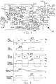
- FIG. 3 illustrates a preferred embodiment of a switched-mode CCFL power supply in accordance with the present invention referred to by the general reference character 100.
- the CCFL power supply 100 includes a power N-channel metal-oxide-silicon field effect transistor ("MOSFET") gate-controlled first semiconductor switch 102.
- the first semiconductor switch 102 includes a drain terminal 104 which connects to a first end 106 of a primary winding 108 of a step-up transformer 112.
- a second end 114 of the primary winding 108 connects to a positive voltage power-source terminal 116 through which a voltage V IN , usually ranging between five (5) and twenty-four (24) volts dc, is supplied to the CCFL power supply 100.
- V IN usually ranging between five (5) and twenty-four (24) volts dc
- a source terminal 122 of a P-channel MOSFET gate-controlled second semiconductor switch 124 also connects to the power-source terminal 116.
- a capacitor 126 couples a drain terminal 128 of the second semiconductor switch 124 both to the drain terminal 104 of the first semiconductor switch 102, and also to the primary winding 108 of the step-up transformer 112. The capacitor 126 is oriented so its positive polarity terminal connects to the drain terminal 104 of the first semiconductor switch 102.
- Both the first semiconductor switch 102 and the second semiconductor switch 124 respectively include an integral reverse diode.
- the first semiconductor switch 102 and the second semiconductor switch 124 are preferably model Si9939DY MOSFETs marketed by Siliconix, Inc. of Santa Clara, California.
- a secondary winding 132 of the step-up transformer 112 connects in series with a decoupling capacitor 134.
- a CCFL 136 connects in series with a terminal of the decoupling capacitor 134 and an end of the secondary winding 132, which constitute power output terminals for the CCFL power supply 100.
- a linear permeability ferrite material that does not saturate during normal operation of the CCFL power supply 100 forms a core of the step-up transformer 112.
- the step-up transformer 112 has a ratio between the number of turns in the secondary winding 132, N 2 , and the number of turns in the primary winding 108, N 1 , that is at least 10:1, and generally ranges between 50:1 to 100:1.
- the CCFL power supply 100 preferably employs a pulse-width-modulation controller IC 142 for supplying a N-channel MOSFET driving signal from a N-channel drive output pin 144 to a gate terminal 146 of the first semiconductor switch 102 (that may also be called a control terminal of the first semiconductor switch 102), and a P-channel MOSFET driving signal from a P-channel drive output pin 148 to a gate terminal 152 of the second semiconductor switch 124 (that may also be called a control terminal of the second semiconductor switch 124).
- a pulse-width-modulation controller IC 142 for supplying a N-channel MOSFET driving signal from a N-channel drive output pin 144 to a gate terminal 146 of the first semiconductor switch 102 (that may also be called a control terminal of the first semiconductor switch 102), and a P-channel MOSFET driving signal from a P-channel drive output pin 148 to a gate terminal 152 of the second semiconductor switch 124 (that may also be called a control terminal of
- the controller IC 142 In addition to providing driving signals to the first semiconductor switch 102 and to the second semiconductor switch 124, as explained in greater detail below, the controller IC 142 also provides other functions such as current sensing, feedback compensation, dimming control, duty cycle limit, and a clock oscillator needed for operation of the CCFL power supply 100.
- the controller IC 142 includes a ground pin 158 that electrically connects the controller IC 142 to circuit ground, and a voltage input-pin 162 that connects the controller IC 142 to the power-source terminal 116.
- the voltage input-pin 162 connects to a source terminal 164 of a field effect transistor ("FET") 166, and to an under-voltage lockout circuit 168.
- An output terminal 172 of the under-voltage lockout circuit 168 connects to a gate terminal 174 of the FET 166.
- FET field effect transistor
- the controller IC 142 also includes an enable pin 176 that connects within the controller IC 142 to the under-voltage lockout circuit 168. Applying a specified voltage to the enable pin 176 causes the under-voltage lockout circuit 168 to turn-off the FET 166 even if the voltage supplied to the voltage input-pin 162 exceeds the threshold pre-established by the under-voltage lockout circuit 168.
- the enable pin 176 permits an electrical power management computer program, executed by a central processing unit (“CPU") included in a portable computer, to conveniently manage the computer's electrical power consumption by electrically turning-off and turning-on LCD backlighting.
- CPU central processing unit
- a drain terminal 178 of the FET 166 supplies electrical power to an oscillator 182, to a set-reset flip-flop 184, to a N-channel current amplifier 186, and to an inverting P-channel current amplifier 188.
- a resistor terminal 192 of the oscillator 182 connects to a resistor pin 194 of the controller IC 142.
- a capacitor terminal 196 of the oscillator 182 connects to a capacitor pin 198 of the controller IC 142.
- a timing resistor 202 and a timing capacitor 204 connect respectively between the resistor pin 194 and the capacitor pin 198 and circuit ground. The resistance of the timing resistor 202 and the capacitance of the timing capacitor 204 are selected so the oscillator 182 oscillates at a frequency of approximately 100 to 150 kilohertz ("KHz").
- the oscillator 182 supplies a signal at this 100 to 150 KHz frequency from an output terminal 206 to a set input-terminal 208 for setting the set-reset flip-flop 184.
- the capacitor terminal 196 of the oscillator 182 and the capacitor pin 198 of the controller IC 142 also connect to a non-inverting input-terminal 212 of a comparator 214.
- a sawtooth waveform present at the capacitor pin 198 of the controller IC 142 exceeds a voltage present at an inverting input 216 of the comparator 214, the comparator 214 transmits an output signal to a reset input-terminal 218 that resets the set-reset flip-flop 184. In this way, the oscillator 182 and the comparator 214 alternatively set and reset the set-reset flip-flop 184 at the operating frequency of the oscillator 182.
- the set-reset flip-flop 184 supplies an output signal to an input of a break-before-make circuit 222.
- the break-before-make circuit 222 supplies separate output signals to inputs respectively of the N-channel current amplifier 186 and of the P-channel current amplifier 188.
- Output signals from the N-channel current amplifier 186 and the P-channel current amplifier 188 are respectively coupled to the N-channel drive output pin 144 and the P-channel drive output pin 148 for supplying driving signals to the gate terminals 146 and 152 of the gate-controlled semiconductor switches 102 and 124.
- the first semiconductor switch 102 and the second semiconductor switch 124 operate in a complementary duty-cycle mode. Consequently, the driving signals supplied to the gate terminals 146 and 152 respectively of the gate-controlled semiconductor switches 102 and 124 by the controller IC 142 alternatively turns-on one switch 102 or 124 while turning-off the other switch 102 or 124.
- the break-before-make circuit 222 included in the controller IC 142 ensures that both gate-controlled semiconductor switches 102 and 124 are not both turned-on concurrently.
- a current-sensing resistor 232 couples a source terminal 234 of the first semiconductor switch 102 to circuit ground.
- a voltage present on the current-sensing resistor 232 is supplied through a feedback resistor 236 to a feedback-voltage input-pin 238 of the controller IC 142.
- this feedback voltage is supplied to an inverting input-terminal 242 of an error amplifier 244.
- An output terminal 246 of the error amplifier 244 is coupled within the controller IC 142 to a feedback-capacitor pin 248 of the controller IC 142.
- a feedback capacitor 252 is coupled between the feedback-capacitor pin 248 and the feedback-voltage input-pin 238.
- the error amplifier 244 operates as an integrator for the feedback voltage signal supplied to the feedback resistor 236.
- the error amplifier 244 also includes internal resistive feedback, not illustrated in FIG. 3, which stabilizes the amplifier's DC output voltage and limits the maximum DC gain of the error amplifier 244. Consequently, the output signal from the error amplifier 244 responds relatively slowly, e.g. in milliseconds, to comparatively long-term changes in the average voltage appearing across the current-sensing resistor 232.
- the controller IC 142 also includes a voltage reference 262.
- the voltage reference 262 applies a constant voltage to a first terminal of a first voltage-divider resistor 264 that has second terminal connected to a non-inverting input-terminal 266 of the error amplifier 244.
- a dimming-control input-pin 272 of the controller IC 142 connects the resistor 268 in parallel both with a LCD dimming-control variable-resistor 274 and with a filter capacitor 276.
- the parallel connected resistors 268 and 274 connect in series with the resistor 264 to divide the constant voltage supplied by the voltage reference 262.
- the error amplifier 244 compares the voltage supplied by this voltage divider to the non-inverting input-terminal 266 with the feedback voltage which the inverting input-terminal 242 receives from the current-sensing resistor 232.
- the output signal from the output terminal 246 of the error amplifier 244, which is proportional to the difference between the voltages applied to the inverting input-terminal 242 and the non-inverting input-terminal 266, is supplied as a reference voltage to the inverting input 216 of the comparator 214.
- the voltage of the signal produced by the error amplifier 244 controls the location along the sawtooth waveform supplied to the non-inverting input-terminal 212 at which the output signal from the comparator 214 resets the set-reset flip-flop 184.
- the controller IC 142 also includes a zener diode 282 connected between the inverting input 216 of the comparator 214 and circuit ground.
- the breakdown voltage of the zener diode 282 is selected so the maximum voltage applied to the inverting input 216 of the comparator 214 restricts the duty cycle of the first semiconductor switch 102 to less than a pre-established maximum of 67%. That is, the zener diode 282 limits the voltage applied to the inverting input 216 of the comparator 214 to a maximum value which causes the on-interval for the first semiconductor switch 102 to be no more than twice as long as the on-interval for the second semiconductor switch 124.
- time t 1 on a second-switch gate-waveform 302, that depicts a voltage between the gate terminal 152 and the drain terminal 128 of the second semiconductor switch 124 marks a beginning of a positive half-cycle of the driving signals applied to the gate terminals 146 and 152 of the gate-controlled semiconductor switches 102 and 124.
- the second semiconductor switch 124 is turned-off by the signal supplied from the P-channel drive output pin 148 of the second semiconductor switch 124.
- a first-switch gate-waveform 304 that depicts a voltage between the gate terminal 146 and the source terminal 234 of the first semiconductor switch 102
- the signal transmitted from the N-channel drive output pin 144 of the controller IC 142 turns-on the first semiconductor switch 102.
- a primary-winding voltage-waveform 306 turning-on of the first semiconductor switch 102 at time t 2 applies a positive voltage across the primary winding 108 from the first end 106 to the second end 114.
- Application of this voltage across the primary winding 108 causes current to flow through the primary winding 108 and the first semiconductor switch 102, as indicated by an arrow in FIG. 3 labeled I P , and as illustrated by the first-switch drain-to-source current waveform 308 I DS in FIG. 4.
- a fraction of the current flowing through the first semiconductor switch 102 constitutes a magnetization current I M for a core of the step-up transformer 112.
- the magnetization current I M depicted in FIG. 4 by a magnetizing current-waveform 314, increases at a rate V IN /L p , where L p is an inductance of the primary winding 108 of the step-up transformer 112.
- the current flowing through the first semiconductor switch 102 I P depicted by the first-switch drain-to-source current waveform 308, equals the sum of the magnetization current I M plus the reflected current flowing through CCFL 136, i.e. I P ⁇ I M + I S ⁇ (N 2 /N 1 ) where N w and N 1 are respectively the number of turns in the primary winding 108 and in the secondary winding 132 of the step-up transformer 112.
- the first semiconductor switch 102 turns-off marking a beginning of a negative half-cycle of voltage across the primary winding 108.
- the voltages across the primary winding 108 and the secondary winding 132 reverse as illustrated by the primary-winding voltage-waveform 306 in FIG. 4. Reversal of the voltage across the primary winding 108 causes current to flow in a loop through the series connected capacitor 126 and second semiconductor switch 124, initially through the reverse diode integrated into the second semiconductor switch 124.
- the magnetization current I M begins to decrease as indicated by the magnetizing current-waveform 314.
- the second semiconductor switch 124 Shortly after t 3 , at time t 4 on the second-switch gate-waveform 302, the second semiconductor switch 124 turns-on. When the second semiconductor switch 124 turns-on, most of the current flowing through the primary winding 108 of the step-up transformer 112 then flows from the drain terminal 128 to the source terminal 122 of the second semiconductor switch 124, rather than through the reverse diode integrated into the second semiconductor switch 124.
- Time t 5 on the second-switch gate-waveform 302 marks an end of the negative half-cycle of voltage across the primary winding 108, and indicates the instant at which the second semiconductor switch 124 turns-off. Turning-off of the second semiconductor switch 124 restores the operating state of the CCFL power supply 100 to that existing at the time T 1 .
- One method for analyzing operation of the CCFL power supply 100 during the negative half-cycles i.e. from time t 3 -t 4 to time t 5 -t 1 , considers the inductance of the step-up transformer 112 and the capacitance of the capacitor 126 as forming a parallel resonant circuit with the CCFL 136 being a load connected in parallel both with the primary winding 108 and with the capacitor 126. Analyzed in this way, the resonant frequency of the step-up transformer 112 and the capacitor 126 must be much lower than the actual operating frequency of the CCFL power supply 100.
- the inductance of the step-up transformer 112 and the capacitance of the capacitor 126 are selected to establish a resonant frequency such that operating frequency of the CCFL power supply 100 is preferably seven (7) to ten (10) times greater than the resonant frequency.
- operating frequency of the CCFL power supply 100 is preferably seven (7) to ten (10) times greater than the resonant frequency.
- I P the current flowing through the primary winding 108
- I P powers the operation of the CCFL 136
- the other half of I P increases energy stored in the inductance of the step-up transformer 112.
- energy stored in the inductance of the step-up transformer 112 powers the operation of the CCFL 136.
- the CCFL power supply 100 supplies power to the CCFL 136, i.e. to the load of the step-up transformer 112, both during each positive half-cycle and during each negative half-cycle in the operation of the CCFL power supply 100.
- the amount of power which the CCFL power supply 100 supplies to the CCFL 136 is proportional to the voltage applied between the power-source terminal 116 and circuit ground multiplied by the average current flowing from the power-source terminal 116 to circuit ground.
- the average voltage applied to the feedback resistor 236 at the junction of the source terminal 234 of the first semiconductor switch 102 with the current-sensing resistor 232 is proportional to the current flowing from the power-source terminal 116 to circuit ground.
- Operation of the controller IC 142 adjusts the respective duty cycles of the gate-controlled semiconductor switches 102 and 124 to stabilize the average current flowing through the current-sensing resistor 232, and, correspondingly, the average current flowing between the power-source terminal 116 and circuit ground through the primary winding 108 of the step-up transformer 112.
- the relative amount of the current flowing through the current-sensing resistor 232 may be varied by adjusting the resistance of the LCD dimming-control variable-resistor 274. Changing the resistance of the LCD dimming-control variable-resistor 274 either increases or decreases the magnitude of the feedback stabilized average current flowing through the current-sensing resistor 232, i.e. the average current flowing between the power-source terminal 116 and circuit ground through the primary winding 108 of the step-up transformer 112.
- the overall electrical efficiency of the CCFL power supply 100 is significantly higher than the electrical efficiency of the current-fed Royer circuit 10' depicted in FIG. 2.
- the current-fed Royer circuit 10' has an efficiency of approximately 70-80%
- a properly constructed CCFL power supply 100 in accordance with the present invention has an efficiency of approximately 90%. Since LCD backlighting consumes approximately 20% to 30% of the electrical power required to operate a portable computer, a 10% to 20% decrease in the amount of power required to backlight an LCD increases the operating time provided by a fully charged battery by approximately 2% to 6%.
- a CCFL power supply 100 in accordance with the present invention preferably includes MOSFETs for the gate-controlled semiconductor switches 102 and 124
- a circuit in accordance with the present invention could be implemented using bipolar transistors that are connected in parallel with discrete diodes.
- the MOSFET gate-controlled semiconductor switches 102 and 124 would be replaced by bipolar NPN transistors.
- the source of the MOSFET would be exchanged for the emitter of a bipolar transistor
- the gate of the MOSFET would be exchanged for the base of a bipolar transistor
- the drain of the MOSFET would be exchanged for the collector of the bipolar transistor.
- the order of the series connected second semiconductor switch 124 and capacitor 126 could be reversed from that disclosed above for the preferred embodiment, although a more complicated controller IC 142 would then be required for supplying the control signal to the gate terminal 152 of the second semiconductor switch 124.
- the core of the step-up transformer 112 is preferably made from a linear permeability ferrite material, it could also be made from a non-linear permeability ferrite material, although the use of such a non-linear permeability material would reduce the conversion efficiency of the CCFL power supply 100.
Landscapes
- Engineering & Computer Science (AREA)
- Power Engineering (AREA)
- Dc-Dc Converters (AREA)
- Circuit Arrangements For Discharge Lamps (AREA)
- Inverter Devices (AREA)
Applications Claiming Priority (2)
| Application Number | Priority Date | Filing Date | Title |
|---|---|---|---|
| US633221 | 1996-04-16 | ||
| US08/633,221 US5619402A (en) | 1996-04-16 | 1996-04-16 | Higher-efficiency cold-cathode fluorescent lamp power supply |
Publications (3)
| Publication Number | Publication Date |
|---|---|
| EP0802702A2 true EP0802702A2 (de) | 1997-10-22 |
| EP0802702A3 EP0802702A3 (de) | 1998-11-04 |
| EP0802702B1 EP0802702B1 (de) | 2000-09-06 |
Family
ID=24538752
Family Applications (1)
| Application Number | Title | Priority Date | Filing Date |
|---|---|---|---|
| EP97105722A Expired - Lifetime EP0802702B1 (de) | 1996-04-16 | 1997-04-07 | Vorschaltgerät mit höher Wirksamkeit für elektrodenlose Floureszenzlampe |
Country Status (6)
| Country | Link |
|---|---|
| US (1) | US5619402A (de) |
| EP (1) | EP0802702B1 (de) |
| JP (1) | JP3533405B2 (de) |
| CA (1) | CA2200932A1 (de) |
| DE (1) | DE69702998T2 (de) |
| TW (1) | TW331067B (de) |
Cited By (1)
| Publication number | Priority date | Publication date | Assignee | Title |
|---|---|---|---|---|
| CN102111936A (zh) * | 2010-11-26 | 2011-06-29 | 深圳市聚作实业有限公司 | Led驱动电源 |
Families Citing this family (108)
| Publication number | Priority date | Publication date | Assignee | Title |
|---|---|---|---|---|
| US5777867A (en) * | 1995-09-14 | 1998-07-07 | Suitomo Electric Industries, Ltd. | Electric discharge method and apparatus |
| US5930121A (en) * | 1997-03-14 | 1999-07-27 | Linfinity Microelectronics | Direct drive backlight system |
| US5923129A (en) * | 1997-03-14 | 1999-07-13 | Linfinity Microelectronics | Apparatus and method for starting a fluorescent lamp |
| US6207943B1 (en) | 1997-10-30 | 2001-03-27 | Baker Electronics, Inc. | Consistent brightness backlight system |
| US6099145A (en) * | 1997-10-30 | 2000-08-08 | Baker Electronics, Inc. | Enhanced MTBF backlight system and related method |
| US6895448B2 (en) * | 1998-03-26 | 2005-05-17 | O2 Micro, Inc. | Low-power audio CD player for portable computers |
| US6954804B2 (en) * | 1998-03-26 | 2005-10-11 | Micro, Inc. | Controller for portable electronic devices |
| US6675233B1 (en) * | 1998-03-26 | 2004-01-06 | O2 Micro International Limited | Audio controller for portable electronic devices |
| US5892336A (en) * | 1998-05-26 | 1999-04-06 | O2Micro Int Ltd | Circuit for energizing cold-cathode fluorescent lamps |
| US6900600B2 (en) | 1998-12-11 | 2005-05-31 | Monolithic Power Systems, Inc. | Method for starting a discharge lamp using high energy initial pulse |
| US6114814A (en) * | 1998-12-11 | 2000-09-05 | Monolithic Power Systems, Inc. | Apparatus for controlling a discharge lamp in a backlighted display |
| US6104146A (en) * | 1999-02-12 | 2000-08-15 | Micro International Limited | Balanced power supply circuit for multiple cold-cathode fluorescent lamps |
| US6946806B1 (en) | 2000-06-22 | 2005-09-20 | Microsemi Corporation | Method and apparatus for controlling minimum brightness of a fluorescent lamp |
| US6198234B1 (en) | 1999-06-09 | 2001-03-06 | Linfinity Microelectronics | Dimmable backlight system |
| US6804129B2 (en) * | 1999-07-22 | 2004-10-12 | 02 Micro International Limited | High-efficiency adaptive DC/AC converter |
| US6259615B1 (en) | 1999-07-22 | 2001-07-10 | O2 Micro International Limited | High-efficiency adaptive DC/AC converter |
| US6349386B1 (en) | 1999-08-24 | 2002-02-19 | 02 Micro International Limited | Launch key, low power CD-ROM player for portable computers |
| JP3233138B2 (ja) | 1999-09-27 | 2001-11-26 | 松下電器産業株式会社 | インバータ回路 |
| DE19948903C2 (de) * | 1999-10-11 | 2002-07-18 | Infineon Technologies Ag | Getaktete Stromversorgung |
| DE60122727T2 (de) | 2000-05-12 | 2007-09-13 | 02 Micro International Ltd. | Intregrierte schaltung zur lampenerwärmung und dimmersteuerung |
| US7130930B1 (en) * | 2000-06-16 | 2006-10-31 | O2 Micro Inc. | Low power CD-ROM player with CD-ROM subsystem for portable computer capable of playing audio CDs without supply energy to CPU |
| US6307765B1 (en) | 2000-06-22 | 2001-10-23 | Linfinity Microelectronics | Method and apparatus for controlling minimum brightness of a fluorescent lamp |
| US7890741B2 (en) * | 2000-12-01 | 2011-02-15 | O2Micro International Limited | Low power digital audio decoding/playing system for computing devices |
| US7522965B2 (en) * | 2000-12-01 | 2009-04-21 | O2Micro International Limited | Low power digital audio decoding/playing system for computing devices |
| US7818443B2 (en) * | 2000-12-01 | 2010-10-19 | O2Micro International Ltd. | Low power digital audio decoding/playing system for computing devices |
| US7526349B2 (en) * | 2000-12-01 | 2009-04-28 | O2Micro International Limited | Low power digital audio decoding/playing system for computing devices |
| US7522964B2 (en) | 2000-12-01 | 2009-04-21 | O2Micro International Limited | Low power digital audio decoding/playing system for computing devices |
| US7522966B2 (en) * | 2000-12-01 | 2009-04-21 | O2Micro International Limited | Low power digital audio decoding/playing system for computing devices |
| US6501234B2 (en) | 2001-01-09 | 2002-12-31 | 02 Micro International Limited | Sequential burst mode activation circuit |
| KR20020060842A (ko) * | 2001-01-12 | 2002-07-19 | 오투 마이크로 인터내셔널 리미티드 | 고효율 적응 직류/교류 컨버터 |
| US6448838B1 (en) * | 2001-03-16 | 2002-09-10 | Semiconductor Components Industries Llc | Circuit and method for high-speed break-before-make electronic switch |
| US6509696B2 (en) * | 2001-03-22 | 2003-01-21 | Koninklijke Philips Electronics N.V. | Method and system for driving a capacitively coupled fluorescent lamp |
| US6570344B2 (en) | 2001-05-07 | 2003-05-27 | O2Micro International Limited | Lamp grounding and leakage current detection system |
| US6741061B2 (en) * | 2001-05-24 | 2004-05-25 | Comair Rotron, Inc. | Efficient stator |
| TW536862B (en) * | 2001-10-22 | 2003-06-11 | Chi Mei Electronic Corp | Power supply circuit for cold cathode fluorescent lamp |
| US7515446B2 (en) * | 2002-04-24 | 2009-04-07 | O2Micro International Limited | High-efficiency adaptive DC/AC converter |
| US6856519B2 (en) | 2002-05-06 | 2005-02-15 | O2Micro International Limited | Inverter controller |
| KR100857848B1 (ko) * | 2002-05-17 | 2008-09-10 | 삼성전자주식회사 | 백라이트 어셈블리와 이의 구동 방법과 이를 갖는 액정 표시 장치 |
| US6879111B2 (en) * | 2002-05-29 | 2005-04-12 | Delphi Technologies, Inc. | DC/AC and DC/DC power supply for LCD displays |
| US6873322B2 (en) * | 2002-06-07 | 2005-03-29 | 02Micro International Limited | Adaptive LCD power supply circuit |
| US6756769B2 (en) | 2002-06-20 | 2004-06-29 | O2Micro International Limited | Enabling circuit for avoiding negative voltage transients |
| US6949912B2 (en) | 2002-06-20 | 2005-09-27 | 02Micro International Limited | Enabling circuit for avoiding negative voltage transients |
| US6924667B2 (en) * | 2002-07-19 | 2005-08-02 | O2Micro International Limited | Level shifting and level-shifting amplifier circuits |
| JP4156324B2 (ja) | 2002-09-30 | 2008-09-24 | ローム株式会社 | 直流−交流変換装置、及び交流電力供給方法 |
| US6940233B2 (en) | 2002-10-03 | 2005-09-06 | Analog Microelectronics, Inc. | Method and system of driving a CCFL |
| US6979959B2 (en) * | 2002-12-13 | 2005-12-27 | Microsemi Corporation | Apparatus and method for striking a fluorescent lamp |
| CN100435466C (zh) | 2002-12-25 | 2008-11-19 | 罗姆股份有限公司 | 直流-交流转换装置的并行运转系统及控制器集成电路 |
| JP3672034B2 (ja) | 2002-12-25 | 2005-07-13 | ローム株式会社 | 直流−交流変換装置、及びそのコントローラic |
| US6778415B2 (en) * | 2003-01-22 | 2004-08-17 | O2Micro, Inc. | Controller electrical power circuit supplying energy to a display device |
| US7102870B2 (en) * | 2003-02-11 | 2006-09-05 | Taser International, Inc. | Systems and methods for managing battery power in an electronic disabling device |
| US7145762B2 (en) * | 2003-02-11 | 2006-12-05 | Taser International, Inc. | Systems and methods for immobilizing using plural energy stores |
| US7057611B2 (en) * | 2003-03-25 | 2006-06-06 | 02Micro International Limited | Integrated power supply for an LCD panel |
| US6936975B2 (en) * | 2003-04-15 | 2005-08-30 | 02Micro International Limited | Power supply for an LCD panel |
| US6897698B1 (en) * | 2003-05-30 | 2005-05-24 | O2Micro International Limited | Phase shifting and PWM driving circuits and methods |
| KR100552903B1 (ko) * | 2003-06-03 | 2006-02-22 | 엘지.필립스 엘시디 주식회사 | 액정표시장치의 램프 구동장치 |
| RU2271079C2 (ru) * | 2003-07-31 | 2006-02-27 | Общество с ограниченной ответственностью ООО "Юник Ай Сиз" | Импульсный источник питания флуоресцентных ламп с холодным катодом |
| US7187139B2 (en) * | 2003-09-09 | 2007-03-06 | Microsemi Corporation | Split phase inverters for CCFL backlight system |
| US7183727B2 (en) * | 2003-09-23 | 2007-02-27 | Microsemi Corporation | Optical and temperature feedbacks to control display brightness |
| US6919694B2 (en) | 2003-10-02 | 2005-07-19 | Monolithic Power Systems, Inc. | Fixed operating frequency inverter for cold cathode fluorescent lamp having strike frequency adjusted by voltage to current phase relationship |
| ES2340169T3 (es) | 2003-10-06 | 2010-05-31 | Microsemi Corporation | Esquema de distribucion de corrientes y dispositivo para operar multiples lamparas ccf. |
| US7602597B2 (en) * | 2003-10-07 | 2009-10-13 | Taser International, Inc. | Systems and methods for immobilization using charge delivery |
| US7030569B2 (en) * | 2003-10-16 | 2006-04-18 | Analog Microelectronics, Inc. | Direct drive CCFL circuit with controlled start-up mode |
| US7279851B2 (en) * | 2003-10-21 | 2007-10-09 | Microsemi Corporation | Systems and methods for fault protection in a balancing transformer |
| WO2005045311A2 (en) * | 2003-11-03 | 2005-05-19 | Monolithic Power Systems, Inc. | Driver for light source having integrated photosensitive elements for driver control |
| US7187140B2 (en) * | 2003-12-16 | 2007-03-06 | Microsemi Corporation | Lamp current control using profile synthesizer |
| TW200527809A (en) * | 2004-01-27 | 2005-08-16 | Rohm Co Ltd | DC-AC converter, controller IC there for, and an electronic apparatus using such DC-AC converter |
| US7468722B2 (en) | 2004-02-09 | 2008-12-23 | Microsemi Corporation | Method and apparatus to control display brightness with ambient light correction |
| US7394209B2 (en) * | 2004-02-11 | 2008-07-01 | 02 Micro International Limited | Liquid crystal display system with lamp feedback |
| TWI342659B (en) | 2004-03-05 | 2011-05-21 | Rohm Co Ltd | Dc-ac converter, controller ic thereof, and electronic device using such dc-ac converter |
| US7112929B2 (en) * | 2004-04-01 | 2006-09-26 | Microsemi Corporation | Full-bridge and half-bridge compatible driver timing schedule for direct drive backlight system |
| US7250731B2 (en) * | 2004-04-07 | 2007-07-31 | Microsemi Corporation | Primary side current balancing scheme for multiple CCF lamp operation |
| US7755595B2 (en) | 2004-06-07 | 2010-07-13 | Microsemi Corporation | Dual-slope brightness control for transflective displays |
| US7012380B2 (en) * | 2004-06-24 | 2006-03-14 | Dell Products L.P. | Information handling system with dual mode inverter |
| WO2006019888A2 (en) * | 2004-07-26 | 2006-02-23 | Microsemi Corporation | Push-pull driver with null-short feature |
| US7323829B2 (en) * | 2004-08-20 | 2008-01-29 | Monolithic Power Systems, Inc. | Minimizing bond wire power losses in integrated circuit full bridge CCFL drivers |
| TWI318084B (en) | 2004-10-13 | 2009-12-01 | Monolithic Power Systems Inc | Methods and protection schemes for driving discharge lamps in large panel applications |
| US7148633B2 (en) * | 2004-10-18 | 2006-12-12 | Beyond Innovation Technology | DC/AC inverter |
| TWI345430B (en) * | 2005-01-19 | 2011-07-11 | Monolithic Power Systems Inc | Method and apparatus for dc to ac power conversion for driving discharge lamps |
| US7061183B1 (en) | 2005-03-31 | 2006-06-13 | Microsemi Corporation | Zigzag topology for balancing current among paralleled gas discharge lamps |
| US7173382B2 (en) * | 2005-03-31 | 2007-02-06 | Microsemi Corporation | Nested balancing topology for balancing current among multiple lamps |
| US7439685B2 (en) * | 2005-07-06 | 2008-10-21 | Monolithic Power Systems, Inc. | Current balancing technique with magnetic integration for fluorescent lamps |
| US7420829B2 (en) | 2005-08-25 | 2008-09-02 | Monolithic Power Systems, Inc. | Hybrid control for discharge lamps |
| US7778004B2 (en) * | 2005-09-13 | 2010-08-17 | Taser International, Inc. | Systems and methods for modular electronic weaponry |
| US7291991B2 (en) * | 2005-10-13 | 2007-11-06 | Monolithic Power Systems, Inc. | Matrix inverter for driving multiple discharge lamps |
| CN1953631A (zh) * | 2005-10-17 | 2007-04-25 | 美国芯源系统股份有限公司 | 一种适合冷阴极荧光灯背光应用的直流/交流电源装置 |
| US7423384B2 (en) | 2005-11-08 | 2008-09-09 | Monolithic Power Systems, Inc. | Lamp voltage feedback system and method for open lamp protection and shorted lamp protection |
| US7414371B1 (en) | 2005-11-21 | 2008-08-19 | Microsemi Corporation | Voltage regulation loop with variable gain control for inverter circuit |
| US7394203B2 (en) * | 2005-12-15 | 2008-07-01 | Monolithic Power Systems, Inc. | Method and system for open lamp protection |
| US7619371B2 (en) * | 2006-04-11 | 2009-11-17 | Monolithic Power Systems, Inc. | Inverter for driving backlight devices in a large LCD panel |
| US7804254B2 (en) * | 2006-04-19 | 2010-09-28 | Monolithic Power Systems, Inc. | Method and circuit for short-circuit and over-current protection in a discharge lamp system |
| US7317783B2 (en) * | 2006-04-21 | 2008-01-08 | Pavel Dolgonos | Reduced X-Ray exposure using power modulation |
| US7420337B2 (en) * | 2006-05-31 | 2008-09-02 | Monolithic Power Systems, Inc. | System and method for open lamp protection |
| US7569998B2 (en) | 2006-07-06 | 2009-08-04 | Microsemi Corporation | Striking and open lamp regulation for CCFL controller |
| US7768806B2 (en) | 2006-12-11 | 2010-08-03 | O2Micro International Limited | Mixed-code DC/AC inverter |
| KR101342961B1 (ko) * | 2007-03-26 | 2013-12-18 | 삼성디스플레이 주식회사 | 인버터, 이를 갖는 백라이트 어셈블리 및 이를 갖는표시장치 |
| JP2008289319A (ja) * | 2007-05-21 | 2008-11-27 | Sanken Electric Co Ltd | 放電管電力供給装置及び半導体集積回路 |
| JP4277127B2 (ja) * | 2007-08-22 | 2009-06-10 | サンケン電気株式会社 | 交流電源装置 |
| CN101388175B (zh) * | 2007-09-14 | 2010-12-08 | 群康科技(深圳)有限公司 | 背光控制电路及其控制方法 |
| CN101453818B (zh) * | 2007-11-29 | 2014-03-19 | 杭州茂力半导体技术有限公司 | 放电灯的电路保护和调节装置 |
| TW200939886A (en) | 2008-02-05 | 2009-09-16 | Microsemi Corp | Balancing arrangement with reduced amount of balancing transformers |
| JP2010035271A (ja) | 2008-07-25 | 2010-02-12 | Sanken Electric Co Ltd | 電力変換装置 |
| US8093839B2 (en) * | 2008-11-20 | 2012-01-10 | Microsemi Corporation | Method and apparatus for driving CCFL at low burst duty cycle rates |
| TWI538553B (zh) | 2009-08-25 | 2016-06-11 | 皇家飛利浦電子股份有限公司 | 多通道照明單元及供應電流至其光源之驅動器 |
| US9030119B2 (en) | 2010-07-19 | 2015-05-12 | Microsemi Corporation | LED string driver arrangement with non-dissipative current balancer |
| US8754581B2 (en) | 2011-05-03 | 2014-06-17 | Microsemi Corporation | High efficiency LED driving method for odd number of LED strings |
| WO2012151170A1 (en) | 2011-05-03 | 2012-11-08 | Microsemi Corporation | High efficiency led driving method |
| US8619440B2 (en) * | 2011-09-20 | 2013-12-31 | Leadtrend Technology Corp. | Over current protection method used in a switched-mode power supply and related controller |
| CN103025033B (zh) * | 2013-01-11 | 2015-01-28 | 淮南市矿用电器设备有限责任公司 | 通用型矿用led灯驱动器 |
Family Cites Families (20)
| Publication number | Priority date | Publication date | Assignee | Title |
|---|---|---|---|---|
| US3596165A (en) * | 1969-07-24 | 1971-07-27 | Tektronix Inc | Converter circuit having a controlled output |
| US4441146A (en) * | 1982-02-04 | 1984-04-03 | Vicor Corporation | Optimal resetting of the transformer's core in single ended forward converters |
| GB2170663B (en) * | 1985-02-02 | 1989-06-14 | Brian Ernest Attwood | Harmonic-resonant power supply |
| US4763237A (en) * | 1986-10-17 | 1988-08-09 | Wieczorek John P | DC/AC/DC Power conversion system including parallel transformers |
| US4809148A (en) * | 1987-10-21 | 1989-02-28 | British Columbia Telephone Company | Full-fluxed, single-ended DC converter |
| US5019749A (en) * | 1988-05-10 | 1991-05-28 | Seiko Epson Corporation | Back-light device for a video display apparatus |
| CA2019525C (en) * | 1989-06-23 | 1995-07-11 | Takuya Ishii | Switching power supply device |
| JPH0734653B2 (ja) * | 1989-09-05 | 1995-04-12 | 九州大学長 | 電源装置 |
| JPH0748944B2 (ja) * | 1989-10-14 | 1995-05-24 | 東光株式会社 | Dc―dcコンバータ |
| US5109328A (en) * | 1989-10-24 | 1992-04-28 | Kijima Co., Ltd. | Push-pull inverter employing current feedback |
| US4959764A (en) * | 1989-11-14 | 1990-09-25 | Computer Products, Inc. | DC/DC converter switching at zero voltage |
| ATE143738T1 (de) * | 1990-07-13 | 1996-10-15 | Andre Bonnet | Magnetisches steuerverfahren von energieübertragung in einem statischen konverter |
| US5140510A (en) * | 1991-03-04 | 1992-08-18 | Motorola, Inc. | Constant frequency power converter |
| US5206800A (en) * | 1991-03-13 | 1993-04-27 | Astec International, Ltd. | Zero voltage switching power converter with secondary side regulation |
| DE4313359A1 (de) * | 1992-04-24 | 1993-10-28 | Matsushita Electric Industrial Co Ltd | Schaltnetzteil |
| ES2056747B1 (es) * | 1993-03-31 | 1997-10-16 | Alcatel Standard Electrica | Circuito de conversion de continua-continua. |
| US5430633A (en) * | 1993-09-14 | 1995-07-04 | Astec International, Ltd. | Multi-resonant clamped flyback converter |
| JP3374301B2 (ja) * | 1994-07-07 | 2003-02-04 | 株式会社キジマ | プッシュプルインバ−タ |
| US5615093A (en) * | 1994-08-05 | 1997-03-25 | Linfinity Microelectronics | Current synchronous zero voltage switching resonant topology |
| JP3312369B2 (ja) * | 1994-11-15 | 2002-08-05 | ミネベア株式会社 | インバータ装置 |
-
1996
- 1996-04-16 US US08/633,221 patent/US5619402A/en not_active Expired - Lifetime
- 1996-11-28 TW TW085114713A patent/TW331067B/zh not_active IP Right Cessation
-
1997
- 1997-03-25 CA CA002200932A patent/CA2200932A1/en not_active Abandoned
- 1997-03-27 JP JP11414897A patent/JP3533405B2/ja not_active Expired - Fee Related
- 1997-04-07 EP EP97105722A patent/EP0802702B1/de not_active Expired - Lifetime
- 1997-04-07 DE DE69702998T patent/DE69702998T2/de not_active Expired - Lifetime
Cited By (1)
| Publication number | Priority date | Publication date | Assignee | Title |
|---|---|---|---|---|
| CN102111936A (zh) * | 2010-11-26 | 2011-06-29 | 深圳市聚作实业有限公司 | Led驱动电源 |
Also Published As
| Publication number | Publication date |
|---|---|
| TW331067B (en) | 1998-05-01 |
| US5619402A (en) | 1997-04-08 |
| CA2200932A1 (en) | 1997-10-16 |
| DE69702998D1 (de) | 2000-10-12 |
| JP3533405B2 (ja) | 2004-05-31 |
| EP0802702B1 (de) | 2000-09-06 |
| JPH1050489A (ja) | 1998-02-20 |
| DE69702998T2 (de) | 2001-04-12 |
| EP0802702A3 (de) | 1998-11-04 |
Similar Documents
| Publication | Publication Date | Title |
|---|---|---|
| US5619402A (en) | Higher-efficiency cold-cathode fluorescent lamp power supply | |
| US6969958B2 (en) | Square wave drive system | |
| KR100983703B1 (ko) | 직류-교류 변환 장치 및 교류 전력 공급 방법 | |
| US6011360A (en) | High efficiency dimmable cold cathode fluorescent lamp ballast | |
| US6198236B1 (en) | Methods and apparatus for controlling the intensity of a fluorescent lamp | |
| US5396155A (en) | Self-dimming electronic ballast | |
| US20070008751A1 (en) | DC-AC converter, and method for supplying AC power | |
| US7548028B2 (en) | Current-mode resonant inverter circuit | |
| US7825605B2 (en) | DA/AC convert for driving cold cathode fluorescent lamp | |
| KR20000068973A (ko) | 대기 모드 동작을 위한 전원 장치 | |
| US6532159B2 (en) | Switching power supply unit | |
| US6788005B2 (en) | Inverter and lamp ignition system using the same | |
| JP4125120B2 (ja) | Lcd装置及びlcdバックライト用インバータ回路 | |
| JP4063625B2 (ja) | 放電灯点灯装置 | |
| CN101223831B (zh) | 自激式反相器驱动电路 | |
| WO2000038305A1 (en) | A synchronous flyback converter | |
| KR880000509B1 (ko) | 정출력 특성의 전자식 방전등 점등 장치 | |
| JP2000133484A (ja) | 放電管駆動回路 | |
| KR960003949B1 (ko) | 영전압 스위칭 방식의 공진형 컨버터 | |
| RU2144286C1 (ru) | Стабилизированный преобразователь напряжения для люминесцентной лампы | |
| JP3319882B2 (ja) | 放電灯点灯装置 | |
| JPH076892A (ja) | 調光用放電灯点灯装置 | |
| KR20030068756A (ko) | 인버터와 이를 사용한 램프 점화 시스템 | |
| JPH08126348A (ja) | Dc−acインバータ | |
| JP2002335675A (ja) | 同期整流回路 |
Legal Events
| Date | Code | Title | Description |
|---|---|---|---|
| PUAI | Public reference made under article 153(3) epc to a published international application that has entered the european phase |
Free format text: ORIGINAL CODE: 0009012 |
|
| AK | Designated contracting states |
Kind code of ref document: A2 Designated state(s): DE FR GB IT |
|
| 17P | Request for examination filed |
Effective date: 19980219 |
|
| PUAL | Search report despatched |
Free format text: ORIGINAL CODE: 0009013 |
|
| AK | Designated contracting states |
Kind code of ref document: A3 Designated state(s): DE FR GB IT |
|
| GRAG | Despatch of communication of intention to grant |
Free format text: ORIGINAL CODE: EPIDOS AGRA |
|
| 17Q | First examination report despatched |
Effective date: 19990210 |
|
| GRAG | Despatch of communication of intention to grant |
Free format text: ORIGINAL CODE: EPIDOS AGRA |
|
| GRAH | Despatch of communication of intention to grant a patent |
Free format text: ORIGINAL CODE: EPIDOS IGRA |
|
| GRAH | Despatch of communication of intention to grant a patent |
Free format text: ORIGINAL CODE: EPIDOS IGRA |
|
| GRAA | (expected) grant |
Free format text: ORIGINAL CODE: 0009210 |
|
| RIC1 | Information provided on ipc code assigned before grant |
Free format text: 7H 05B 41/292 A, 7H 05B 41/28 B |
|
| AK | Designated contracting states |
Kind code of ref document: B1 Designated state(s): DE FR GB IT |
|
| PG25 | Lapsed in a contracting state [announced via postgrant information from national office to epo] |
Ref country code: IT Free format text: LAPSE BECAUSE OF FAILURE TO SUBMIT A TRANSLATION OF THE DESCRIPTION OR TO PAY THE FEE WITHIN THE PRESCRIBED TIME-LIMIT;WARNING: LAPSES OF ITALIAN PATENTS WITH EFFECTIVE DATE BEFORE 2007 MAY HAVE OCCURRED AT ANY TIME BEFORE 2007. THE CORRECT EFFECTIVE DATE MAY BE DIFFERENT FROM THE ONE RECORDED. Effective date: 20000906 |
|
| REF | Corresponds to: |
Ref document number: 69702998 Country of ref document: DE Date of ref document: 20001012 |
|
| ET | Fr: translation filed | ||
| PLBE | No opposition filed within time limit |
Free format text: ORIGINAL CODE: 0009261 |
|
| STAA | Information on the status of an ep patent application or granted ep patent |
Free format text: STATUS: NO OPPOSITION FILED WITHIN TIME LIMIT |
|
| 26N | No opposition filed | ||
| REG | Reference to a national code |
Ref country code: GB Ref legal event code: IF02 |
|
| PGFP | Annual fee paid to national office [announced via postgrant information from national office to epo] |
Ref country code: DE Payment date: 20130429 Year of fee payment: 17 Ref country code: GB Payment date: 20130429 Year of fee payment: 17 |
|
| PGFP | Annual fee paid to national office [announced via postgrant information from national office to epo] |
Ref country code: FR Payment date: 20130506 Year of fee payment: 17 |
|
| REG | Reference to a national code |
Ref country code: DE Ref legal event code: R119 Ref document number: 69702998 Country of ref document: DE |
|
| GBPC | Gb: european patent ceased through non-payment of renewal fee |
Effective date: 20140407 |
|
| REG | Reference to a national code |
Ref country code: FR Ref legal event code: ST Effective date: 20141231 |
|
| PG25 | Lapsed in a contracting state [announced via postgrant information from national office to epo] |
Ref country code: GB Free format text: LAPSE BECAUSE OF NON-PAYMENT OF DUE FEES Effective date: 20140407 Ref country code: DE Free format text: LAPSE BECAUSE OF NON-PAYMENT OF DUE FEES Effective date: 20141101 |
|
| REG | Reference to a national code |
Ref country code: DE Ref legal event code: R119 Ref document number: 69702998 Country of ref document: DE Effective date: 20141101 |
|
| PG25 | Lapsed in a contracting state [announced via postgrant information from national office to epo] |
Ref country code: FR Free format text: LAPSE BECAUSE OF NON-PAYMENT OF DUE FEES Effective date: 20140430 |