EP0790502A2 - Sonde, ihre Herstellung und von ihr Gebrauch machende vertikal arbeitende Testsondenanordnung - Google Patents
Sonde, ihre Herstellung und von ihr Gebrauch machende vertikal arbeitende Testsondenanordnung Download PDFInfo
- Publication number
- EP0790502A2 EP0790502A2 EP97300909A EP97300909A EP0790502A2 EP 0790502 A2 EP0790502 A2 EP 0790502A2 EP 97300909 A EP97300909 A EP 97300909A EP 97300909 A EP97300909 A EP 97300909A EP 0790502 A2 EP0790502 A2 EP 0790502A2
- Authority
- EP
- European Patent Office
- Prior art keywords
- probe
- board
- probes
- contact
- buckling
- Prior art date
- Legal status (The legal status is an assumption and is not a legal conclusion. Google has not performed a legal analysis and makes no representation as to the accuracy of the status listed.)
- Withdrawn
Links
- 239000000523 sample Substances 0.000 title claims abstract description 477
- 238000004519 manufacturing process Methods 0.000 title claims description 23
- 238000005259 measurement Methods 0.000 claims abstract description 62
- 239000004065 semiconductor Substances 0.000 claims abstract description 47
- 238000000034 method Methods 0.000 claims description 21
- 238000010438 heat treatment Methods 0.000 claims description 16
- 229910000679 solder Inorganic materials 0.000 claims description 16
- 239000000463 material Substances 0.000 claims description 14
- 230000008569 process Effects 0.000 claims description 12
- 238000005452 bending Methods 0.000 claims description 10
- 229920005989 resin Polymers 0.000 claims description 9
- 239000011347 resin Substances 0.000 claims description 9
- 238000002844 melting Methods 0.000 claims description 8
- 238000010891 electric arc Methods 0.000 claims description 4
- 239000011248 coating agent Substances 0.000 claims description 3
- 238000000576 coating method Methods 0.000 claims description 3
- 238000003825 pressing Methods 0.000 claims 1
- WFKWXMTUELFFGS-UHFFFAOYSA-N tungsten Chemical compound [W] WFKWXMTUELFFGS-UHFFFAOYSA-N 0.000 description 13
- 229910052721 tungsten Inorganic materials 0.000 description 10
- 239000010937 tungsten Substances 0.000 description 10
- 229910052751 metal Inorganic materials 0.000 description 8
- 239000002184 metal Substances 0.000 description 8
- 125000006850 spacer group Chemical group 0.000 description 8
- 230000009471 action Effects 0.000 description 7
- RYGMFSIKBFXOCR-UHFFFAOYSA-N Copper Chemical compound [Cu] RYGMFSIKBFXOCR-UHFFFAOYSA-N 0.000 description 6
- 238000005476 soldering Methods 0.000 description 6
- 235000012431 wafers Nutrition 0.000 description 6
- 229910052782 aluminium Inorganic materials 0.000 description 5
- XAGFODPZIPBFFR-UHFFFAOYSA-N aluminium Chemical compound [Al] XAGFODPZIPBFFR-UHFFFAOYSA-N 0.000 description 5
- 238000005498 polishing Methods 0.000 description 5
- 239000012298 atmosphere Substances 0.000 description 4
- 238000005520 cutting process Methods 0.000 description 4
- 230000000694 effects Effects 0.000 description 4
- 239000000919 ceramic Substances 0.000 description 3
- 230000008859 change Effects 0.000 description 3
- 238000004140 cleaning Methods 0.000 description 3
- 229910052802 copper Inorganic materials 0.000 description 3
- 239000010949 copper Substances 0.000 description 3
- 239000011889 copper foil Substances 0.000 description 3
- 239000003822 epoxy resin Substances 0.000 description 3
- 238000005530 etching Methods 0.000 description 3
- 230000006698 induction Effects 0.000 description 3
- 230000007246 mechanism Effects 0.000 description 3
- 229920000647 polyepoxide Polymers 0.000 description 3
- 239000007787 solid Substances 0.000 description 3
- PXHVJJICTQNCMI-UHFFFAOYSA-N Nickel Chemical compound [Ni] PXHVJJICTQNCMI-UHFFFAOYSA-N 0.000 description 2
- VYPSYNLAJGMNEJ-UHFFFAOYSA-N Silicium dioxide Chemical compound O=[Si]=O VYPSYNLAJGMNEJ-UHFFFAOYSA-N 0.000 description 2
- 239000000853 adhesive Substances 0.000 description 2
- 230000001070 adhesive effect Effects 0.000 description 2
- 230000003064 anti-oxidating effect Effects 0.000 description 2
- 230000003078 antioxidant effect Effects 0.000 description 2
- 238000013459 approach Methods 0.000 description 2
- 230000015572 biosynthetic process Effects 0.000 description 2
- PCHJSUWPFVWCPO-UHFFFAOYSA-N gold Chemical compound [Au] PCHJSUWPFVWCPO-UHFFFAOYSA-N 0.000 description 2
- 229910052737 gold Inorganic materials 0.000 description 2
- 239000010931 gold Substances 0.000 description 2
- 239000001307 helium Substances 0.000 description 2
- 229910052734 helium Inorganic materials 0.000 description 2
- SWQJXJOGLNCZEY-UHFFFAOYSA-N helium atom Chemical compound [He] SWQJXJOGLNCZEY-UHFFFAOYSA-N 0.000 description 2
- 238000009413 insulation Methods 0.000 description 2
- 229910052741 iridium Inorganic materials 0.000 description 2
- 238000003475 lamination Methods 0.000 description 2
- 230000008018 melting Effects 0.000 description 2
- 238000010417 needlework Methods 0.000 description 2
- 229910052763 palladium Inorganic materials 0.000 description 2
- 239000004033 plastic Substances 0.000 description 2
- 229920003023 plastic Polymers 0.000 description 2
- 229910052697 platinum Inorganic materials 0.000 description 2
- 229920001721 polyimide Polymers 0.000 description 2
- 229910052703 rhodium Inorganic materials 0.000 description 2
- 230000000087 stabilizing effect Effects 0.000 description 2
- 239000000758 substrate Substances 0.000 description 2
- XUIMIQQOPSSXEZ-UHFFFAOYSA-N Silicon Chemical compound [Si] XUIMIQQOPSSXEZ-UHFFFAOYSA-N 0.000 description 1
- BQCADISMDOOEFD-UHFFFAOYSA-N Silver Chemical compound [Ag] BQCADISMDOOEFD-UHFFFAOYSA-N 0.000 description 1
- PNEYBMLMFCGWSK-UHFFFAOYSA-N aluminium oxide Inorganic materials [O-2].[O-2].[O-2].[Al+3].[Al+3] PNEYBMLMFCGWSK-UHFFFAOYSA-N 0.000 description 1
- 230000005540 biological transmission Effects 0.000 description 1
- 238000004891 communication Methods 0.000 description 1
- 239000000470 constituent Substances 0.000 description 1
- 230000007547 defect Effects 0.000 description 1
- 238000013461 design Methods 0.000 description 1
- 239000000945 filler Substances 0.000 description 1
- -1 for instance Substances 0.000 description 1
- LNEPOXFFQSENCJ-UHFFFAOYSA-N haloperidol Chemical compound C1CC(O)(C=2C=CC(Cl)=CC=2)CCN1CCCC(=O)C1=CC=C(F)C=C1 LNEPOXFFQSENCJ-UHFFFAOYSA-N 0.000 description 1
- 239000001257 hydrogen Substances 0.000 description 1
- 229910052739 hydrogen Inorganic materials 0.000 description 1
- 239000011261 inert gas Substances 0.000 description 1
- 238000003780 insertion Methods 0.000 description 1
- 230000037431 insertion Effects 0.000 description 1
- 238000003754 machining Methods 0.000 description 1
- 238000012423 maintenance Methods 0.000 description 1
- 239000000155 melt Substances 0.000 description 1
- 150000002739 metals Chemical class 0.000 description 1
- 229910052759 nickel Inorganic materials 0.000 description 1
- 239000012299 nitrogen atmosphere Substances 0.000 description 1
- 229910000510 noble metal Inorganic materials 0.000 description 1
- 238000007500 overflow downdraw method Methods 0.000 description 1
- 230000003647 oxidation Effects 0.000 description 1
- 238000007254 oxidation reaction Methods 0.000 description 1
- 238000007747 plating Methods 0.000 description 1
- 238000004663 powder metallurgy Methods 0.000 description 1
- 238000012545 processing Methods 0.000 description 1
- 239000012858 resilient material Substances 0.000 description 1
- 238000000926 separation method Methods 0.000 description 1
- 238000004904 shortening Methods 0.000 description 1
- 229910052710 silicon Inorganic materials 0.000 description 1
- 239000010703 silicon Substances 0.000 description 1
- 239000000377 silicon dioxide Substances 0.000 description 1
- 229910052709 silver Inorganic materials 0.000 description 1
- 239000004332 silver Substances 0.000 description 1
- 239000000725 suspension Substances 0.000 description 1
Images










Classifications
-
- G—PHYSICS
- G01—MEASURING; TESTING
- G01R—MEASURING ELECTRIC VARIABLES; MEASURING MAGNETIC VARIABLES
- G01R1/00—Details of instruments or arrangements of the types included in groups G01R5/00 - G01R13/00 and G01R31/00
- G01R1/02—General constructional details
- G01R1/06—Measuring leads; Measuring probes
- G01R1/067—Measuring probes
- G01R1/07—Non contact-making probes
-
- G—PHYSICS
- G01—MEASURING; TESTING
- G01R—MEASURING ELECTRIC VARIABLES; MEASURING MAGNETIC VARIABLES
- G01R3/00—Apparatus or processes specially adapted for the manufacture or maintenance of measuring instruments, e.g. of probe tips
-
- G—PHYSICS
- G01—MEASURING; TESTING
- G01R—MEASURING ELECTRIC VARIABLES; MEASURING MAGNETIC VARIABLES
- G01R1/00—Details of instruments or arrangements of the types included in groups G01R5/00 - G01R13/00 and G01R31/00
- G01R1/02—General constructional details
- G01R1/06—Measuring leads; Measuring probes
- G01R1/067—Measuring probes
- G01R1/06711—Probe needles; Cantilever beams; "Bump" contacts; Replaceable probe pins
- G01R1/06716—Elastic
-
- G—PHYSICS
- G01—MEASURING; TESTING
- G01R—MEASURING ELECTRIC VARIABLES; MEASURING MAGNETIC VARIABLES
- G01R1/00—Details of instruments or arrangements of the types included in groups G01R5/00 - G01R13/00 and G01R31/00
- G01R1/02—General constructional details
- G01R1/06—Measuring leads; Measuring probes
- G01R1/067—Measuring probes
- G01R1/073—Multiple probes
- G01R1/07307—Multiple probes with individual probe elements, e.g. needles, cantilever beams or bump contacts, fixed in relation to each other, e.g. bed of nails fixture or probe card
- G01R1/07357—Multiple probes with individual probe elements, e.g. needles, cantilever beams or bump contacts, fixed in relation to each other, e.g. bed of nails fixture or probe card with flexible bodies, e.g. buckling beams
Definitions
- This invention relates to a probe for measuring electrical characteristics of a semiconductor integrated circuit, manufacture of the same, and a probe card assembly of vertically operative type employing the same which avoids undesireable contact and offers convenience in the work of exchanging a probe.
- the concept of the probe card assembly is explained in U.S. Patent No. 5,134,365 granted July 28, 1992.
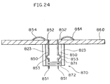
- a conventional art of the vertically operative type probe card assembly includes, as shown in Fig. 24, a plurality of probes 850, and board 860 fastening probes 850, and housing members 870 mounted on the underside of board 860.
- the probe 850 is generally shaped in a needle work, of which a front part includes contact portion 851 for contacting onto electrode 710 of semiconductor integrated circuit 700 and a back part includes connecting portion 852 to be connected by connector 854, such as gold line, to a wiring pattern formed on board 860.
- flexible portion 853 in a generally lateral U shape is formed between contact portion 851 and connecting portion 852.
- the flexible portion 853 is intended, as shown in Fig. 25, to bend or flex for keeping a desired contact pressure when a contact is made between contact portion 851 and electrode 710.
- Housing members 870 include two guide boards 871, 872 provided with through holes 871A, 872A, and a pair of walls 823 for fastening two guide boards 871, 872 with board 860.
- Through holes 871A, 872A in two guide boards 871, 872 are provided for insertion of contact portions 851 of probes 850 and arranged to align to positional pattern of electrodes 710 of semiconductor integrated circuit 700 for measurement.
- board 860 is provided on its upperside with predetermined wiring pattern (not shown) and with a through hole 861 into which connecting portion 852 of probe 850 is inserted. See Fig. 25. Connecting portion 852 inserted in through hole 861 will be connected to the wiring pattern above.
- a conventional probe card assembly has had such measurements as: about 6 mm vertical thickness of the board, about 10 mm vertical length of the housing members, thus a probe has been about 20 mm length.
- Recent semiconductor integrated circuits have much progressed in employing higher speed signals and in turn require best shorter probes and wiring patterns in order to minimize signal attenuation and cross-talk troubles in advance.
- the probe length employed in the probe card assembly of vertically operative type has at shortest about 20 mm in the state of art, though further shortening has been desired as to probe length.
- probes have been normally manufactured from tungsten wires which were produced by drawing tungsten rods manufactured by powder metallurgy. For this cause, drawing of tungsten wire extends flaw or defect to extend along the length of probes, so that cut sections of the drawn tungsten wires, that is, contact portions have more trend of forming irregularities, and thus the probe contact portions are easier to attract foreign matters than other portions.
- the probes which have been applied to contact with electrodes are subject to cleaning for removing foreign matters from the contact portions. Otherwise the prior step is taken to make the contact portions round.
- the cleaning requires regular maintenance and as a result causes suspension of the operation employing the probes, and making round contact portions includes difficulty in forming a correct semi circle at the end of the contact portion and also difficulty in processing many probes concurrently, thus poor production efficiency.
- Electrodes are in shapes of semi circular bump. Such electrodes should be applied by probes having a flat end of the contact portion, but such type of probes tends to change the shape of the end by the cleaning and in turn to make it difficult to obtain correct measurements subsequently.
- the present invention intends to offer a probe card assembly of vertically operative type employing shorter length probes with the merit of facilitating the work of exchanging used probes even in the case where so many probes are equipped, and the probes suitable for such application, and process of manufacturing such probes.
- a probe of the present invention features in a shape of generally needle work, and in having a buckling portion to bend or to buckle, upon contact onto an electrode of semiconductor integrated circuit at the end of its contact portion, wherein the probe has a generally round section and its buckling portion is thinner than other portions excepting the end of the contact portion, and the contact portion and the buckling portion are formed to be linear.
- a process for manufacturing a probe of the present invention features generally in the process of manufacturing a probe for making a contact onto an electrode of semiconductor integrated circuit and in including a step of heating up to be molten the contact portion to be used to make a contact onto the electrode, and a step of forming a minuscule ball from the molten part.
- a first probe card assembly configuration of vertically operative type features in including: a plurality of probes having a buckling portion to bend or to buckle, upon a contact by the end of its contact portion onto an electrode of semiconductor integrated circuit; and a first board provided with a first wiring pattern connected with a connecting portion of the probe; and a second board removably fastened with the first board and provided with a second wiring pattern connected with the first wiring pattern; and housing members mounted with the second board for holding the contact portion of the probe; wherein the probe has a generally round section and its buckling portion is thinner than other portions excepting the end of the contact portion, and the contact portion and the buckling portion are formed to be linear, and wherein through holes are provided with the first board for the respective probes inserting through, and second board is provided with space for probes extending through in the state as-suspended from the first board.
- a second probe card assembly configuration of vertically operative type features in including: a plurality of measurement probes provided respectively with buckling portions which will buckle, upon a contact by the end of its contact portion onto electrode of semiconductor integrated circuit; first board provided with wiring pattern connecting to the end of connecting portions of measurement probes; second board superjacent to and fastened removably with first board; a plurality of connection probes provided respectively with buckling portions which will buckle, upon a contact by the end of contact portion onto wiring pattern when inserted into through hole provided with second board; wherein the measurement probes and the connection probes are generally round in section, and their buckling portions are thinner than other portions excepting the ends of contact portions, and contact portions and buckling portions are shaped generally to be linear, and wherein the first board is provided with through holes for the measurement probes inserting, and the second board is provided with wiring pattern connecting to the back ends of the connecting portions of the probes for circuit connection.
- a third probe card assembly configuration of vertically operative type features in including: a plurality of probes each provided with contact portion, and buckling portion which will buckle, upon a contact by the end of contact portion to an electrode of semiconductor integrated circuit; a board provided at least on upperside with wiring pattern to which connecting portion of probe is connected; supporting members mounted underside of the board for supporting probes; wherein each probe is generally round and buckling portion thereof is slender than other portions excepting the end of contact portion, and contact and buckling portions are shaped to be linear; and wherein the board is provided with through holes for probes extending through; and the supporting members including; a plurality of probe supporters made from insulative material and provided at periphery with a plurality of flutes for holding probes whose buckling portions take position inside the flutes, and fastening means for fastening removably the probe supporters underside of the board respectively.
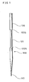
- Fig. 1 shows a schematic front elevation view of a first probe in accordance with an embodiment of the present invention.
- Fig. 2 shows a schematic front elevation view of a probe of an embodiment of the present invention for special purpose of explaining the buckling act.
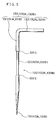
- Fig. 3 shows a schematic front elevation view of a probe in accordance with a second embodiment of the present invention.
- Fig. 4 shows a schematic front elevation view of a probe in accordance with a third embodiment of the present invention.
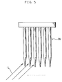
- Fig. 5 shows a schematic view for explaining a first process of manufacturing probes in accordance with an embodiment of the present invention.
- Fig. 6 shows a schematic view for explaining a second process of manufacturing probes in accordance with an embodiment of the present invention.
- Fig. 7 shows a schematic view for explaining a third process of manufacturing probes in accordance with an embodiment of the present invention.
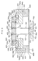
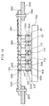
- Fig. 8 shows a schematic, vertically sectioned elevation view of a first probe card assembly of vertically operative type in accordance with an embodiment of the present invention.
- Fig. 9 shows a schematic view of the first probe card assembly in action.
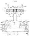
- Fig. 10 shows a schematic, exploded view of the first probe card assembly.
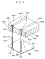
- Fig. 11 shows a partially cutaway, perspective view of key portions of the first probe card assembly.
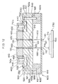
- Fig. 12 shows a schematic, vertically sectioned view of a second probe card assembly of vertically operative type in accordance with an embodiment of the present invention.
- Fig. 13 shows a schematic view of key portions of the second probe card assembly in action.
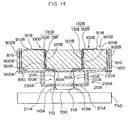
- Fig. 14 shows a schematic view of a third probe card assembly of vertically operative type belonging to an embodiment of the present invention.
- Fig. 15 shows a schematic, exploded view of the third probe card assembly.
- Fig. 16 shows a schematic, partially cutaway perspective view of a fourth probe card assembly of vertically operative type belonging to an embodiment of the present invention.
- Fig. 17 shows a schematic, exploded view of the fourth probe card assembly.
- Fig. 18 shows a schematic, vertically sectioned elevation view of a fifth probe card assembly of vertically operative type belonging to an embodiment of the present invention.
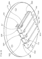
- Fig. 19 shows a schematic perspective view from below of the fifth probe card assembly.
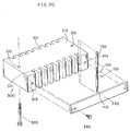
- Fig. 20 shows a schematic, exploded perspective view of a supporter assembled in the fifth probe card assembly.
- Fig. 21 shows a schematic sectional view explaining connection between a board included in the fifth assembly and a connecting portion of the probe.
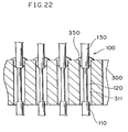
- Fig. 22 shows a schematic sectional view explaining connection between a probe supporter and probes.
- Fig. 23 shows a schematic sectional view explaining arrangement of probes in a flute.
- Fig. 24 shows a schematic, vertically sectioned elevation view of a probe card assembly of vertically operative type belonging to the conventional related art.
- Fig. 25 shows a schematic sectional view of the conventional probe card assembly in action, wherein sub-figures (A) and (B) are included.
- probe configuration In summary, these 25 figures are grouped into 4 groups: probe configuration, manufacture of probes, probe card assembly configuration, related art.
- Figs. 1 to 4 are for probe confirguration wherein three embodiments are shown (Fig. 1 for 1st, Fig. 3 for 2nd, Fig. 4 for 3rd.).
- Figs. 5 to 7 are for manufacture of probes wherein three embodiments are shown (Fig. 5 for 1st, Fig. 6 for 2nd, Fig. 7 for 3rd.).
- Fig. 8 to 23 are for probe card assembly wherein five embodiment configurations are shown (Figs 8 to 11 for 1st, Figs. 12 to 13 for 2nd, Figs. 14 to 15 for 3rd, Figs. 16 to 17 for 4th, Figs. 18 to 23 for 5th.).
- Figs 24 to 25 are for related art in contrast to the present invention.
- a first probe is characterized, as shown in Fig. 1, in that a probe 100 is shaped as a whole to be linear like a needle and generally round in section, and includes buckling portion 120 which is thinner or slenderized stepwise 102S than two other connected portions 110, 130 excepting the end of contact portion 110.
- FIG. 7 Another feature of the probe 100 lies in some case in an extreme end of contact portion 110, though such is not detailed in Fig. 1, but supplemented by Figs. 5 to 7. That is, a minuscule ball is formed at that end (see Fig. 7 wherein the ball is shown not to size), and that end is covered or plated with a metal anti-oxidative, low resistive, high electrical conductive, such as Rh, Pd, Ir, Pt.
- the contact end covered with such a metal avoids attachment of aluminum which is a material constituting an electrode 610 and thereby contact portion 110 is less susceptible against the oxidation with a result of stabilizing the contact resistance value involved in measurements.
- Forming a minuscule ball at the extreme front end of contact portion 110 is carried out by the method of heating the end of contact portion 110 and waiting for the surface tension effecting over molten part, that is, the method of utilizing the natural action.
- Heat-melting of the end of contact portion 110 is performed by irradiation of laser ray as shown in Fig. 5, or heating by the high frequency coil as shown in Fig. 6, or heating by the arc discharge.
- tungsten wires W 1000 units (0.25 mm dia.) which are nickel plated and whose contact portions 110 are sharpened with the electrolytic polishing, and these tungsten wires are arranged 20 units x 50 units with lmm interval each other and fastened keeping the contact portions (pointed point in Fig. 5) downward.
- YAG laser ray L (for instance, 75 watt, beam dia.: about 0.1 to 0.2 mm) is irradiated in pulse waves focussing on contact portions 110, wherein YAG laser ray is focussed from two sources located at 45 degrees left and right.
- YAG lasing instantly heat-melts contact portions 110 of tungsten wires W and the lasing focus is moved to next wires, wherein amount of melting effect is controlled by pulse speed of the YAG lasing.
- the heat melting by YAG lasing L prefers unoxidizing atmosphere, such as helium or nitrogen atmosphere, but air atmosphere may be employed in the case of noble metals or anti-oxidative metals.
- a plurality of tungsten wires are arranged with suitable interval (normally about 1 mm) wherein a high frequency induction coil C is set to encompass adjacent to contact portions 110 of the wires (sharpened in Fig. 6) and the high frequency heating coil C is activated from the high frequency source to heat-melt contact portions 110.
- the arc discharge heating may be employed to heat-melt contact portions 110 of the tungsten wires W, wherein carrying out in inert gas atmosphere is desired.
- minuscule balls 150 are prepared in advance, and these ball materials 150 are heated and fused to tungsten wires or berium copper wires.
- a tungsten wire (0.5 mm dia.) is sharpened by a rotary whetstone to make an end portion so sharp, and a minuscule ball 150 (70 microns dia.) is fuse-attached to the sharpened point by heating in oxygen-hydrogen flame.
- buckling portion 120 is made thinner or slender stepwise 120S than other two portions excepting the end of contact portion 110. For this reason, upon effecting force at contact portion 110, buckling portion 120 will buckle as is expected and shown in Fig. 2, and such property is imparted by polishing by whetson or electrolytic polishing.
- the connecting portion 130 is part for connecting or fastening probe 100 with wiring pattern 310.
- This connecting portion 130 is formed to be linear from buckling portion 120 (see Fig. 1 or 2), and when mounted in place with board 200 (see Figs. 16 to 18 or Fig. 21), connecting portion 130 will extend partially over board 200. This extension may be clipped by a tool (not shown), such as about 1 to 1.5 mm.
- Probe 100 has typically dimensions of buckling portion 120 about 40 microns dia., 3 mm length; contact portion 110 about 2.5 mm length; connecting portion 130 about 3.5 mm length.
- the overdrive is 0.1 mm, wherein the overdrive is defined as vertical push-in length from an initial contact point onto an electrode with the pointed end of the contact portion, contact pressure of 10 g/cubic cm to 20 g/cubic cm is obtained, and when the contact pressure is at 15 g/cubic cm, the contact resistance between the electrode and probe 100 is estimated about 0.5 ohm.
- the present invention does not exclude probes 100 having only sharpened point at the end of contact portion 110 with no minuscule ball 150 as described, so far as the buckling portion 120 functions to give a predetermined contact pressure stably under overdrive condition.
- probe card assembly of vertically operative type employing such probe as explained above will be described with reference to Figs. 8 to 11.
- the term "probe card assembly of vertically operative type” will sometimes be shortened to "this type assembly”, or “the present assembly”, or “the assembly” if such abbreviation is thought to be instantly understandable.
- the first embodiment of probe card assembly of vertically operative type features in including: a plurality of probes 100 having buckling portion 120 to bend or to buckle, upon a contact onto electrode 710 of semiconductor integrated circuit 700 at the end of its contact portion 110; and first board 400 provided with first wiring pattern 420 connected with connecting portion 130 of probe 100; and second board 500 removably fastened with first board 400 and provided with second wiring pattern 520 connected with first wiring pattern 420; and housing members 600 mounted with second board 500 for controlling contact portion 110 of probe 100; wherein probe 100 has a generally round section and its buckling portion 120 is thinner than other portions excepting the end of contact portion 110, and contact portion 110 and buckling portion 120 are formed to be linear, and wherein one through opening 510 is provided with second board 500 for inserting through probes 100 mounted with first board 400 in unitary group as a whole.
- First board 400 is an insulative board provided with a plurality of through holes 410 correspondent to probes 100 in number, and through holes 410 are provided for admitting connecting portions 130 of probes 100 to insert through, and because of linear shape of the probes, these holes 410 are arranged to directly align to positional pattern of electrodes 710 of semiconductor integrated circuit 700 to be tested.
- first wiring pattern 420 formed of etched copper foil is provided for electrically connecting electrodes 710 of semiconductor integrated circuit 700, with aid of probes 100, to a tester (not shown), and its terminal encompasses through hole 410 in the form of land portion 421, to which portion 421 the connecting portion 130 of probe 100 is connected or bonded with solder 450.
- the other terminal of first wiring pattern 420 extends through other through holes 430 and leads out of the underside of first board 400, and in turn forms bump 422 there, as shown in Fig. 10.
- First board 400 thus described has at its corners fastening holes 440 for removably fastening second board 500.
- Second board 500 is provided with one central opening 510 for inserting through probes 100 mounted with first board 400.
- This opening 510 permits all probes 100 constituting the present assembly to extend through, that is to say that all through holes 410 provided in first board 400 are positioned so that all these holes 410 are ranged laterally inside one opening 510 of second board 500 after second board 500 is fastened with first board 400.
- Second board 500 is made from lamination of glass-reinforced epoxy resin plates or polyimide films, wherein second wiring pattern 520 is formed in multilayers, and second wiring pattern 520 in the multilayer form has one terminal 521 exposed on the surface of second board 500 in a form of land portion, wherein its exposure is located to align to bump 422 derived from first wiring pattern 420 as described above, upon second board 500 being fastened with first board 400.
- second board 500 is made from lamination of glass-reinforced epoxy resin plates or polyimide films, wherein second wiring pattern 520 is formed in multilayers, and second wiring pattern 520 in the multilayer form has one terminal 521 exposed on the surface of second board 500 in a form of land portion, wherein its exposure is located to align to bump 422 derived from first wiring pattern 420 as described above, upon second board 500 being fastened with first board 400.
- fastening second board 500 with first board 400 brings about electrical connection between first and second wiring patterns.
- Another end 522 of second pattern 520 is exposed on second board 500 in the form of land portion, and its exposed position is out of first board as fastened, that is, the position where the other end 522 of second wiring pattern 520 is exposed on second board 500, is determined to be at an outer position where first board 400 has not occupied after first board 400 and second board 500 were fastened.
- Second board 500 has fastening holes 530 aligning to fastening holes 440 of first board 400. That is, upon laying second board 500 on first board 400 at the predetermined position, two fastening holes 440, 530 are agreed so that bolt or screw 710S as fastening means will fasten first board 400 with second board 500 removably.
- first wiring pattern 420 in the form of bump 422 located on the underside of first board 400 is connected to end 521 of second wiring pattern 520 at its land portion on the upperside of second board 500.
- second board 500 has through holes 540 for fastening housing materials 600.
- Housing materials 600 include guide panel 610 provided with through holes 611 at positions aligning to probes 100, and spacer 620 for fastening guide panel 610 with the underside of second board 500.
- Spacer 620 has fastening holes 621 positionally aligning to holes 540 of second board 500 as noted. Second board 500 and housing materials 600 are fastened with screw 720S as fastening means by fastening into holes 540, 621.
- the present assembly is set up positionally right above lifter 750 on which a wafer (objective for measurement) is fixed or disposed in place by vacuum sucking.
- Lifter 750 is moved upward from its initial position with the wafer attached, wherein a substrate lifting mechanism (shown under lifter 750 in dotted lines in Fig.
- lifter 750 is lowered to its initial position, and a new wafer is prepared on lifter 750 by vacuum sucking.
- First solder mass 450 which has connected or bonded a probe 100 to be exchanged with first wiring pattern 420 is removed. Thereby physically the probe of interest and first board 400 are separate or disconnected. The probe of interest is pulled away upward out of first board 400, with a result that removal of the probe of interest is complete.
- a new or replacement probe 100 is incorporated to this assembly. First insert new probe 100 into the assembly through the through hole 410 of first board 400 from above. Therein contact portion 110 is certainly inserted through the through hole 611 of guide panel 610 which is aligned to through hole 410 above. The lowest point of contact portion 110 of new probe 100 is correctly positioned or uniformized so as to be at the same level as other probes 100, and then the end of connecting portion 130 is connected or bonded with land portion 421 of first wiring pattern 420 by solder 450.
- second board 500 in the first embodiment as noted before is structured to include one large central opening encompassing all probes equipped inside thereof or all probes extend through one opening at central position.
- second board 500 of the second embodiment is provided with separate through holes for respective probes. Therefore, the second embodiment is different from in this point and in other points much similar to the fist one.
- through holes 510 of the second embodiment are positionally aligned to electrodes 710 of semiconductor integrated circuit 700. That is, through holes 510 of second board 500 are positioned or arranged to align to through holes 410 of first board 400 as well as through holes 611 of guide panel 610 vertically.
- second board 500 is designed to have an enough or abundant length to include buckled portions 120 of probes 100 within the thickness length.
- respective buckling portions 120 are controlled or immobilized by through holes 510 of second board 500 as well as those 611 of guide panel 610, so that contacts between buckled portions 120 of adjacent probes 100 are certainly avoided. Therefore, denser arrangement of probes 100 is permitted.
- the designated figures 12 and 13 illustrate two probes, though, principally proved.
- first solder mass 450 is removed to disconnect probe 100 to be exchanged from first wiring pattern 420 and then probe 100 of interest is pulled away upward out of first board 400. Thus completely removed from the assembly.
- a new or replacement probe 100 is incorporated into this assembly. First insert the new probe 100 into the assembly through the through hole 410 of first board 400 from above. Therein contact portion 110 is certainly inserted through the through hole 611 of guide panel 610 which is aligned to through hole 410 above. The lowest point of contact portion 110 of the new probe 100 is correctly positioned or uniformized so as to be heightwise at the same level as other probes 100, and then the end of connecting portion 130 is connected with land portion 421 of first wiring pattern 420 by solder 450.
- through holes 510 of second board 500 are added to through holes 410 of first board 400, and thereby the work of inserting probes 100 into through holes 410 of first board 400 will facilitate subsequent work of inserting the ends of contact portions 110 of probes 100 into through holes 611 of guide panel 610. This is unique effect with this embodiment and as a whole the exchange work of probes is facilitated.
- through hole 410 of first board 400 is jointed with through hole 510 of second board 500 with independence from adjacent other joint holes, so that probes 100 inserted in adjacent holes are avoided from mutual contact in their buckled state, and choice is available as to positioning buckling portion 120 either in through hole 410 of first board 400 or in through hole 510 of second board 500 and in turn more freedom in determining what length of buckling portion 120 is obtained in adjusting resultant contact pressures to be realized.
- guide panel 610 of housing materials 600 is made of one ply, but the present invention is not limited so, and it may be two or more, wherein more plies or layers will protect the ends of contact portions 110 of probes 100 more certainly from possible positional deviations.
- This type assembly features in including: a plurality of probes for measurement 100A provided respectively with buckling portions 120A which will buckle, upon contacting onto electrode 710 of semiconductor integrated circuit 700 at the end of its contact portion 110A; first board 900A provided with wiring pattern 910A connecting to the end of connecting portions 130A of probes for measurement 100A; second board 900B superjacent to and fastened removably with first board 900A; a plurality of probes for circuit connection 100B provided respectively with buckling portions 120B which will buckle, upon contacting onto wiring pattern 910A at the end of contact portion 110B when inserted into through hole 901B provided with second board 900B.
- the probe for measurement (this term will often be shortened to "measurement probe”) 100A and the probe for circuit connection (this term will often be shortened to “connection probe”) 100B are manufactured from tungsten or like metal wire, and are shaped generally in L-letter. That is, much similar to a probe as shown in Fig. 3 or 4, measurement probes 100A and connection probes 100B each include contact portion 110A, 110B having sharpened front end and connecting portion 130A, 130B, and buckling portion 120A, 120B which is intermediate between contact portion 110A, 110B and connecting portion 130A, 130B, wherein connecting portion 130A, 120B is generally bent at right angles against other portions.
- Such probes for measurement and circuit connection have generally round section.
- the front end of contact portion 110A, 110B is plated by anti-oxidizing and low resistive conductive metal, such as Rh, Pd, Ir, Pt.
- the plating by such metal at the front end of contact portion 110A, 110B imparts more avoidance against attaching with aluminum which is a metal constituting electrode 610, so that contact portion 110A, 110B is of anti-oxidation with a result of stabilizing the contact resistance value.
- Contact portion 120A, 120B is formed to be thinner or slenderized than other portions excepting the end of contact portion 110A, 110B. For this reason, pressure acting on contact portion 110A, 110B from over or from under will buckle or bend buckling portion 120A, 120B as shown in Fig. 14. Whetstone polishing or electrolytic polishing is available for slenderizing buckling portion 120A, 120B.
- Connecting portion 130A is a part for connecting the measurement probe 100A to wiring pattern 910A of first board 900A, and this portion 130A includes vertical sub-portion 131A which extends from buckling portion 120A linearly and lateral sub-portion 132A which bends generally at right angles to extend laterally, so that lateral sub-portion 132A is designed to extend with respect to contact portion 110A as well as buckling portion 120A.
- Connecting portion 130B is a part for connecting the connection probe 100B to wiring pattern for connection 910B of second board 900B, and this portion 130B includes vertical sub-portion 131B which extends from buckling portion 120B linearly and lateral sub-portion 132B which bends generally at right angles to extend laterally, so that lateral sub-portion 132B is designed to extend with respect to contact portion 110B as well as buckling portion 120B.
- connection probes 100B With measurement probes 100A and connection probes 100B thus designed, length of vertical portions from bend point 133A, 133B to the end of contact portion 110A, 110B is set to be the same with all of both probes 100A, 100B. Accordingly, when measurement probes 100A are inserted or mounted into through holes 901A, heightweise positions of the ends of contact portions 110A of respective probes 100A are made uniform, and in the same way, when connection probes 100B are inserted or mounted into through holes 901B, heightwise positions of the ends of contact portions 110B of respective probes 100B are made uniform.
- First board 900A is insulative board and provided with a plurality of through holes 901A at positions to align to arrangement of measurement probes 100A, that is, through hole 901A serves as a space for staying vertical sub-portion 131A of connecting portion 130A of measurement probe 100A.
- this board 900A has at its corners through holes 902A for fastening second board 900B.
- predetermined wiring pattern 910A made from copper foil, for instance, is formed by the etching, for instance.
- Wiring pattern 910A is, as shown in Fig. 14, formed into land portion around through hole 901A. Therein length between through hole 901A and wiring pattern 910A is set to be a little shorter than real length of lateral sub-portion 132A of measurement probe 100A for reassuring connection to measurement probe 100A.
- wiring pattern 910A of first board 900A may be formed of only land portion, or of land and wiring portions. As described later, Such formation is selective for the reason that, the arrangement of measurement probes 100A on first board 900A is necessary to be changed according to a change of arrangement of electrodes 610 of semiconductor integrated circuit 600, though, probes 110B from second board 900B and land portions formed on first board 900A are fixed in positional relationship, and therefore wiring pattern 910A will have variable length on first board 900A.
- probe housing 200A is mounted, which is similar to the housing materials 600 as shown in Figs. 8 and 9, and intended to support or guide contact portions 110A of measurement probes 100A and which includes guide panel 210A provided with through holes 211A and spacer 230A for fastening guide panel 210A with first board 900A.
- Through holes 211A of guide panel 210A are arranged to align to positional pattern of electrodes 610 of semiconductor integrated circuit 600 for measurement.
- first board 900A, and measurement probes 100A and probe housing 200A fastened with first board 900A are structured to align to positional pattern of electrodes 610 of semiconductor integrated circuit 600 for measurement, but wiring pattern 910A is independent of positional pattern of electrodes 610 and then fixed. See two paragraphs above.
- second board 900B this board is made from lamination of glass-reinforced epoxy resin plates or polyimide films, wiring is structured in multilayers (not shown) and is provided with through holes 901B which are for inserting connection probes 100B, wherein the end of contact portion 110B of connection probe 100B is made to extend out of underside of second board 900B.
- second board 900B has at corners through holes 902B for fastening first board 900A.
- predetermined wiring pattern for connection 910B formed of copper film by the etching, for instance, is present for connecting lateral sub-portion 132B of connection probe 100B.
- the end of wiring pattern for connection 910B extends its land portion 911B to a position adjacent to through hole 901B, wherein length between through hole 901B and land portion 911B is made a little shorter than real length of lateral sub-portion 132B of connection probe 100B for reassuring connection with connection probe 100B.
- Wiring pattern for connection 910B mounted on second board 900B is connected to multilayer wiring (not shown) in second board 900B, and this multilayer wiring is connected to a connector (not shown) and in turn to the tester, out of the drawing and also not shown. That is, communication route for signals from semiconductor integrated circuit 600 to the tester is through: measurement probe 100B, wiring pattern for connection 910B, multilayer wiring and then to connector.
- First board 900A and second board 900B are fastened by means 810 formed of bolt-nuts, for instance, and inbetween pad spacers 950 formed of resilient material, for instance, rubber pad spacer, is applied.
- This pad spacer 950 is for reassuring electrical connection between contact portion 110B of connection probe 100B and wiring pattern 910A of first board 100A.
- contact pressure between contact portion 110B and wiring pattern 110B will be suitably adjusted by deformation of the pad spacers 950 between first board 900A and second board 900B.
- connection probe 100B Upon fastening first board 900A with second board 900B, connection probe 100B is pressed at its contact portion 110B onto wiring pattern 910A. For this cause, connection probe 100B buckles, as shown in Fig. 20, at its buckling portion and thereby suitable contact pressure is maintained between contact portion 110B and wiring pattern 910A.
- the present assembly thus structured is applied to measure electrical characteristics of semiconductor integrated circuit 700, meanwhile contact pressure between electrodes 710 and measurement probe 100A is maintained by buckling action of the buckling portion 120A of measurement probe 100A.
- second board 900B is removed from first board 900A and thereby the upperside of first board 900A is exposed. Then, solders which have connected measurement probes 100A with wiring pattern 910A are removed. At the same time, adhesive (not shown) which adheres measurement probes 100A with first board 900A in through holes 901A are cleared out. Thus, measurement probes 100A to be exchanged are physically separated from first board 900A and such probes are pulled away upward from first board 900A. Thus, measurement probes to be exchanged 100A are completely removed.
- New or replacement probes will be incorporated into the present assembly.
- insert contact portion 110A into the predetermined through hole 221A of guide panel 210A certainly.
- contact portion 110A of the new measurement probe 100A is mounted on first board 900A heightwise at the same level with contact portions 110A of other measurement probes 100A.
- connection probe 100B is far unlikely to be damaged since its buckling portion 120B does not repeat buckling actions each measurement time, different from measurement probe 100A.
- the present assembly as described needs the change of components including first board 100A and down to suitable ones, in order to measure electrical characteristics of semiconductor integrated circuit 700 having different wiring pattern of electrodes 710.
- measurement probes 100A and connection probes 100B are suitable to be coated over its surface with such metal as gold, silver, copper or aluminum having low electrical resistance, in order to improve transmission of high frequency signals of interest or to avoid attenuation thereof.
- FIG. 16 and 17 This type assembly features in including: a plurality of probes 100 including buckling portion 120 which will buckle, upon contacting the front end of contact portion 110 onto electrode 710 of semiconductor integrated circuit; board 490 including wiring pattern 491 to be connected to probe 100 at least on its upperside; housing members 480 mounted on underside of board 490 for housing probes 100; wherein probe 100 is generally round in section, and its buckling portion 120 is slender than other portions excepting the end of contact portion 110, and contact portion 110 and buckling portion are shaped to be linear; and wherein board 490 is provided with through holes 492 for inserting through probes 100, and housing members 480 include two guide panels 481 provided with through holes 482 for inserting through probes 100, and mounting members (not shown, but similar to the spacer in previous embodiments) for fastening guide panels 481 with board 490.
- Board 490 is a laminated board, and into through holes 492, probes 100 are inserted and stayed with connection portion 130 kept partially uninserted about 1.0 to 1.5 mm (about a length for catching by clipping tool) out of the upperside, and probes 100 are fixed with through holes 492 by soldering.
- Guide panels 481 include two panels vertically separate and laterally held. Through holes 482 provided with guide panels 481 and through holes 492 provided with board 490, and electrodes 710 of semiconductor integrated circuit 700 are aligned positionally. Hence, one unit of probe 100 is designed to extend through three through holes 481(twice), 492 straightly. As noted, two guide panels upper and lower are provided, so that buckling at buckling portion 120 will hardly cause positional deviation at the end of contact portion 110, that is, positional deviation of contact portion 110 relative to electrode 710 will be effectively held minimum.
- This embodiment of vertically operative type probe card assembly features in including: a plurality of probes 100 each provided with contact portion 110, connecting portion 130, and buckling portion 120 which will buckle, upon contacting the end of contact portion 110 to electrode 710 of semiconductor integrated circuit 700 as explained so far; board 200 provided with wiring pattern 210 to which connecting portion 130 of probe 100 is connected; wherein each probe 100 is generally round and buckling portion 120 thereof is slender than other portions excepting the end of contact portion 110.
- Board 200 is made from insulative material and is provided with a plurality of through holes 220 to align positionally to arrangement of probes 100. Connecting portion 130 of probe 100 is inserted into through hole 220.
- wiring pattern 210 made from copper foil for instance, is formed by the etching for instance.
- Wiring pattern 210 is electrically connected to the tester (not shown) provided outside the drawing through probes 100 from electrodes 710 of semiconductor integrated circuit 700, and wiring pattern 210 extends its end around through hole 220 in the form of land portion, as shown in Fig. 8.
- Probe supporter 310 is made from insulative material including ceramics such as alumina, nitrided silica, nitrided aluminum, or various kinds of plastics.
- Probe supporter 310 is generally shaped in a laterally elongated rectangular solid, at whose longer two edges a plurality of (8 units shown in Fig. 20) vertical recesses or flutes 311 are formed to stay or hold probe(s) 100 in each flute. Intervals between flutes 311 are determined to align to electrodes 710 of semiconductor integrated circuit 700.
- Width of flute 311 is designed to be somewhat larger than diameter of connecting portion 130 of probe 100 to be held, and thickness or height of probe supporter 310, that is, that of flute 311 is determined to be longer than length of buckling portion 120 for the purpose of holding buckling portion 120 certainly within the length of flute 311.
- Vertical through holes 312 for inserting fastening means 320, bolting for instance, are provided at two distant peripheries, and on the side face of the solid for flutes 311 formation, two lateral holes 313 are provided at two distant peripheries for fastening a holding plate 330 with the solid side face to secure probes 100 (8 probes shown in Fig. 20) in position by bolting 340, wherein the same device is set up at the back side, though not shown in Fig. 20.
- Probe supporter 310 is conveniently worked out from generally called, machinable ceramics, for instance, [MIOCERAM 500 (trademark)] produced by HISHIDEN KASEI KK (Japanese Corporation), but not limited to the note here.
- Other acceptable materials are such as tractable or workable to machining work to form flutes 311 and insulative. Therefore, a suitable material may be found not only in ceramics, but also in plastics including reinforced epoxy resins, wherein cutting work to form flutes 311 is feasible by rotary cutter with thin edges or laser ray cutting for use to cut wafers, for instance.
- plate 330 is associated by screws 340 to probe supporter 310 and then fastened thereby, and therethrough, respective probes 100 are arranged so as to have contact portions 110 extended the same length from underside of probe supporter 310 and also to have connecting portions 130 extended the same length from upperside of probe supporter 310.
- a plurality of probe supporters 310 (4 units in Fig. 18) are mounted or fastened by fastening means 320 including bolt-nuts combination. Thereby connecting portions 130 of probes 100 are extended upward from the upperside of board 200 through the through holes 220 of board 200.
- Connecting portion 130 is connected to land portion at periphery of through hole 220 by soldering. Therein connecting portion 130 extends past solder bump 230 a little length (specifically about 1.0 to 1.5 mm) after connected by the soldering.
- connecting portion 130 takes position from through hole 220 of board 200 to inside flute 311 of probe supporter 310, and buckling portion 120 takes position inside flute 311, and contact portion 110 takes position from inside flute 311 to outside thereof.
- a plurality of silicon wafers with semiconductor integrated circuits 700 formed thereon are set on lifter 750 with vacuum sucking mechanism, and then lifter 750 is lifted upward to contact electrodes 710 of semiconductor integrated circuits 700 to the ends of contact portions 110 of probes 100.
- lifter 750 Upon finishing the measurement of electrical characteristics of semiconductor integrated circuit 700, lifter 750 is lowered to prepare for next measurement.
- the damaged probe 100 will be exchanged as below:
- new probe 100 is disposed in place of damaged probe 100 into flute 311 and holding plate 330 is re-fastened and in turn probe supporter 310 including new probe 100 is re-fastened with board 200 and re-soldered to connect all probes 100 to wiring pattern 210.
- damaged probe 100 is not broken in itself, removal thereof is carried out as below: two clipping tools made of electrical current conduction are prepared and these two tools are attached to contact portion 110 by one clip and to connecting portion 130 by the other clip so that damaged but non-broken probe 100 is involved in a circuit through the two clips, and then conduct a several ampere current for several seconds to heat-fuse solder mass which has connected probe 100 to wiring pattern 210. If solder is fused, pull out probe 100 of interest upward and new probe 100 is inserted from upper for replacement, and connecting portion 130 of new probe 100 is connected to wiring pattern 210 by soldering.
- This method does not need steps of removing probe supporter 310 including damaged probe 100 and thereby the exchange work results in simpler.
- probe 100 and flute 311 are related dimensionally like in a rod to sleeve pipe relationship, but the present assembly is not limited to such relationship.
- probe 100 inserted in flute 311 may be fixed by insulative filler or putty resin 350.
- resin 350 fixes buckling portion 120, this portion become unlikely to buckle and thereby application of resin 350 is restricted to area between connecting portion 130 and flute 311, and further in this case, holding panel 330 will act to protect resin 350 from flow out of flute 311.
- probe 100 has been assumed to be linear, but not limited so, but probe 100 may be of L-letter shape, wherein connecting portion 130 of probe 100 includes vertical sub-portion 131 and lateral sub-portion 132 bending about at right angles against vertical sub-portion 131.
- Probe 100 so structured has following advantages.
- its heightwise position of the end of contact portion 110 is uniformized conveniently.
- acts of inserting the end of contact portion 110 of probe 100 into through hole 220 of board 200 and placing lateral sub-portion 132 of connecting portion 130 on the upperside of board 200, will determine heightwise position of contact portion 110.
- L-letter probe 100 is structured to have connecting portion 130 including vertical sub-portion 131 made linear to buckling portion 120 and lateral sub-portion 132 bending about at right angles against vertical sub-portion 131, and this is modified so that the bending part from vertical sub-portion 131 is made to extend upward a little to form extension end 133.
- This extension end 133 is useful in the exchange work by the method of fusing the solder mass with electrical heating as noted before. Specifically extension end 133 makes it convenient to apply clipping tool in place.
- one unit of flute 311 has been allocated to receive or hold one piece of probe 100, but not limited so. For instance, as shown in Fig. 23, it is feasible to place two pieces of probe 100.
- intervals between electrodes 710 of semiconductor integrated circuit 700 are narrower than intervals between flutes 311 wherein machinability to fine parts for flute 311 is difficult. Therein it is likely that intervals of electrodes 710 are partially made narrow.
- this case allows the use of probes 100 coated with insulative coating which at least is applied to surfaces to be placed inside flute 311 of probe supporter 310.
- fixer 360 as noted is recommended.
- the probe of the present invention relates to a probe which features in; having a buckling portion to buckle upon a contact by the end of contact portion onto an electrode of semiconductor integrated circuit; and having a generally round section and the buckling portion made slenderized than other portions excepting the end of contact portion, wherein the contact portion and buckling portion are shaped to be linear.
- a vertically operative type probe card assembly employing the inventive probes makes it convenient to carry out the probe exchange work as compared with conventional case.
- the exchange of probes is allowed without cutting the problem probes. That is, release of the probes from a wiring pattern permits to pull out the probes conveniently from a board. Further in mounting new probes to the board, all needed is to insert the probe into the board and to connect it to a wiring pattern.
- the probe exchange work is remarkably made convenient as compared with conventional case.
- this invention discloses the art of making an extending end of the probe for the connection. Now it is assumed that the probe descried has been damaged. Then, release by fusing with electrical heating is applied, that is, clipping tool is conveniently applied to the extending end and the conduction of a current of several amperes for several seconds readily fuses the solder connection. Thereby pulling out the damaged probe upward is feasible and needed thereafter is to insert a new replacement probe from above. Thus, greatly convenienced.
- the present invention discloses the art of forming an upwardly extending end at the bending point.
- the release work of the probe as noted is convenienced, further in the work of mounting it, the length from upper point of vertical sub-portion to the end of contact portion is made uniform or fixed. Thereby effort in uniformizing heightwise positions of probes is made minimum.
- a probe which has a connecting portion including a vertical sub-portion made linear to a buckling portion and a lateral sub-portion bending at right angles without an upwardly extending end.
- the probe as noted is designed, similar to other probes, to have the same length from the bending point between the lateral sub-portion and vertical sub-portion down to the end of contact portion, the effort of uniformizing positions of contact portions is omitted in much the same way as noted.
- probes are each provided with a minuscule ball at the end of contact portion, and thereby are repulsive to foreign matter adhesion. Accordingly, such trouble is unlikely as aluminum which is a constituent of an electrode will attach to the end of contact portion, and for that cause, otherwise deviated measurement results.
- the process therefor includes the step of heating to melt the end of contact portion which will contact an electrode, and the step of forming the molten mass to a target minuscule ball.
- heating to melt the part to be contacted to an electrode is feasible by irradiation with laser ray, induction heating with high frequency coil, arc discharge for choice.
- alternative method is to press-attach a preformed minuscule ball onto the end of contact portion of a probe. This method is suitable to mass scale production and to lower production cost.
- the present invention includes a probe card assembly of vertically operative type which features: a plurality of probes having a buckling portion to buckle, upon a contact by an end of a contact portion onto an electrode of semiconductor integrated circuit; a first board provided with a first wiring pattern connected with a connecting portion of the probe; a second board removably fastened with the first board and provided with a second wiring pattern connected with the first wiring pattern; housing members mounted with the second board for controlling the contact portion of the probe; wherein the probe has a generally round section and its buckling portion is thinner than other portions excepting the end of the contact portion, and the contact portion and the buckling portion are formed linear, and wherein through holes are provided with the first board for inserting through the respective probes, and second board is provided with a through space for the probe extending through in state as-suspended from the first board.
- the probe is structured for its buckling and contact portions being linear, and the first board is provided with through holes, and therefore, release of connection to wiring pattern formed on first board will permit to pull out the probe from the first board, and further its structure serves for convenience in mounting a new probe.
- the present invention includes a probe card assembly of vertically operative type including: a plurality of measurement probes including buckling portions to buckle, upon a contact by an end of contact portion onto an electrode of semiconductor integrated circuit; first board provided with wiring pattern connected to ends of connecting portions of the measurement probes; second board superjacent to and fastened removably with the first board; a plurality of connection probes including buckling portions to buckle, upon a contact by an end of contact portion onto the wiring pattern provided with the first board when inserted into holes provided with the a second board; wherein through holes provided with the second board are positioned to align to the arrangement of wiring pattern provided with the first board; wherein the measurement probes and connection probes have generally round section and their buckling portions are thinner excepting ends of contact portions, and formed linear; wherein the first board is provided with through holes for measurement probes inserting through, and the second board is provided with wiring pattern for connecting to ends of connection probes.
- the present invention includes a probe card assembly of vertically operative type including: a plurality of probes including contact portion, and buckling portion to buckle, upon a contact by an end of the contact portion onto an electrode of semiconductor integrated circuit; a board provided at least on upperside with wiring pattern to which connecting portion of the probe is connected; supporting members mounted underside of the board for supporting the probes; wherein the probe is generally round and the buckling portion thereof is slender excepting the end of contact portion, and contact and buckling portions are shaped linearly; and wherein the board is provided with through holes for probes extending through; and wherein the supporting members include; a plurality of probe supporters made from insulative material and provided at periphery with a plurality of flutes for holding probes whose buckling portions take position inside the flutes, and fastening means for fastening removably the probe supporters underside of the board.
- the buckling portion of a probe is made slender, and the contact and buckling portions are formed linear, so that exchange of probes is permitted without cutting the problem probe unlike conventional case.
- release of connection between the probe and wiring pattern permits to pull out readily the probe from the board, and in mounting a new probe, needed is to insert a new probe into the board and connecting to the wiring pattern. This is remarkably convenient as compared with conventional case.
- Probe length is made shorter by slenderizing the buckling portion with linearity to the contact portion kept.
- conventional one has buckling portion with the same diameter as other portions wherein the buckling portion was formed by bending the wire to be lateral U-letter shape, and accordingly the total length used for preparing one unit probe is longer in the conventional case.
- target today is a shorter probe, in view of attenuation of signals or cross talk problem in measuring electrical characteristics of recent semiconductor integrated circuit wherein high speed signals are prevail.
- the buckling portion is certainly kept which will buckle upon a contact by contact portion onto an electrode of semiconductor circuit, so that predetermined desired contact pressure is reassured.
- the supporting members includes the holding panel mounted removably which will laterally close the flute. Therefore, even if some lateral force from outside will act thereon, leaving out of the probe from the flute is avoided, and thereby electrical shortcircuit will also be prevented.
- portion of the probe which takes position inside the flute is coated with insulative coating. Thereby more certain insulation is reassured so that no shortcircuit problem will occur and it is made feasible to measure more densified circuit.
- the plurality of the probes are arranged to take certain respective positions, and therefore correct measurement is feasible to more number of probes at once.
Landscapes
- Physics & Mathematics (AREA)
- General Physics & Mathematics (AREA)
- Testing Or Measuring Of Semiconductors Or The Like (AREA)
- Measuring Leads Or Probes (AREA)
Applications Claiming Priority (6)
| Application Number | Priority Date | Filing Date | Title |
|---|---|---|---|
| JP8051053A JP2913617B2 (ja) | 1996-02-13 | 1996-02-13 | 縦型プローブカード |
| JP51053/96 | 1996-02-13 | ||
| JP71512/96 | 1996-02-29 | ||
| JP8071512A JPH09236619A (ja) | 1996-02-29 | 1996-02-29 | 縦型プローブカード |
| JP14108196A JP3592441B2 (ja) | 1996-05-10 | 1996-05-10 | 縦型プローブカード |
| JP141081/96 | 1996-05-10 |
Publications (2)
| Publication Number | Publication Date |
|---|---|
| EP0790502A2 true EP0790502A2 (de) | 1997-08-20 |
| EP0790502A3 EP0790502A3 (de) | 1999-03-17 |
Family
ID=27294181
Family Applications (1)
| Application Number | Title | Priority Date | Filing Date |
|---|---|---|---|
| EP97300909A Withdrawn EP0790502A3 (de) | 1996-02-13 | 1997-02-12 | Sonde, ihre Herstellung und von ihr Gebrauch machende vertikal arbeitende Testsondenanordnung |
Country Status (7)
| Country | Link |
|---|---|
| US (2) | US6294922B1 (de) |
| EP (1) | EP0790502A3 (de) |
| KR (1) | KR100212169B1 (de) |
| CN (1) | CN1129797C (de) |
| CA (1) | CA2197373A1 (de) |
| SG (1) | SG71690A1 (de) |
| TW (1) | TW332863B (de) |
Cited By (5)
| Publication number | Priority date | Publication date | Assignee | Title |
|---|---|---|---|---|
| EP1202337A3 (de) * | 2000-10-24 | 2002-09-18 | Nec Corporation | Testnadel für Testkarte |
| DE19748825B4 (de) * | 1997-11-05 | 2004-09-09 | Feinmetall Gmbh | Prüfkopf mit einer Kontaktiervorrichtung |
| US6806723B2 (en) | 2002-08-14 | 2004-10-19 | Fujitsu Limited | Contactor having contact electrodes formed by laser processing |
| EP1737075A3 (de) * | 2005-06-23 | 2007-05-02 | Feinmetall GmbH | Kontaktiervorrichtung |
| WO2014180596A1 (de) * | 2013-05-08 | 2014-11-13 | Feinmetall Gmbh | Elektrische kontaktiervorrichtung |
Families Citing this family (81)
| Publication number | Priority date | Publication date | Assignee | Title |
|---|---|---|---|---|
| US7349223B2 (en) | 2000-05-23 | 2008-03-25 | Nanonexus, Inc. | Enhanced compliant probe card systems having improved planarity |
| US7247035B2 (en) | 2000-06-20 | 2007-07-24 | Nanonexus, Inc. | Enhanced stress metal spring contactor |
| US6799976B1 (en) | 1999-07-28 | 2004-10-05 | Nanonexus, Inc. | Construction structures and manufacturing processes for integrated circuit wafer probe card assemblies |
| US7382142B2 (en) | 2000-05-23 | 2008-06-03 | Nanonexus, Inc. | High density interconnect system having rapid fabrication cycle |
| US6812718B1 (en) | 1999-05-27 | 2004-11-02 | Nanonexus, Inc. | Massively parallel interface for electronic circuits |
| JP2001074777A (ja) * | 1999-08-31 | 2001-03-23 | Kanai Hiroaki | プローブカード用プローブ針 |
| US7579848B2 (en) | 2000-05-23 | 2009-08-25 | Nanonexus, Inc. | High density interconnect system for IC packages and interconnect assemblies |
| US7952373B2 (en) | 2000-05-23 | 2011-05-31 | Verigy (Singapore) Pte. Ltd. | Construction structures and manufacturing processes for integrated circuit wafer probe card assemblies |
| JP2002231399A (ja) * | 2001-02-02 | 2002-08-16 | Fujitsu Ltd | 半導体装置試験用コンタクタ及びその製造方法 |
| US7071714B2 (en) | 2001-11-02 | 2006-07-04 | Formfactor, Inc. | Method and system for compensating for thermally induced motion of probe cards |
| US6972578B2 (en) | 2001-11-02 | 2005-12-06 | Formfactor, Inc. | Method and system for compensating thermally induced motion of probe cards |
| JP4456325B2 (ja) * | 2002-12-12 | 2010-04-28 | 東京エレクトロン株式会社 | 検査方法及び検査装置 |
| US6924654B2 (en) * | 2003-03-12 | 2005-08-02 | Celerity Research, Inc. | Structures for testing circuits and methods for fabricating the structures |
| JP2004333332A (ja) * | 2003-05-08 | 2004-11-25 | Yamaha Corp | プローブユニット及びその製造方法 |
| JP2004363165A (ja) * | 2003-06-02 | 2004-12-24 | Tokyo Seimitsu Co Ltd | ウェーハ処理装置およびウェーハ処理方法 |
| US6900652B2 (en) * | 2003-06-13 | 2005-05-31 | Solid State Measurements, Inc. | Flexible membrane probe and method of use thereof |
| JP4465995B2 (ja) * | 2003-07-02 | 2010-05-26 | 株式会社日立製作所 | プローブシート、プローブカード、半導体検査装置および半導体装置の製造方法 |
| EP1524529B1 (de) * | 2003-10-13 | 2007-03-21 | Technoprobe S.p.A | Prüfkopf mit vertikalen Prüfnadeln für integrierte Halbleitergeräte |
| US20050174136A1 (en) * | 2004-02-09 | 2005-08-11 | Jiachun Zhou | Test pin back surface in probe apparatus for low wear multiple contacting with conductive elastomer |
| CN100357745C (zh) * | 2004-02-17 | 2007-12-26 | 财团法人工业技术研究院 | 集成化探针卡及组装方式 |
| US20060066328A1 (en) * | 2004-09-30 | 2006-03-30 | Probelogic, Inc. | Buckling beam probe test assembly |
| JP4395429B2 (ja) * | 2004-10-20 | 2010-01-06 | 日本発條株式会社 | コンタクトユニットおよびコンタクトユニットを用いた検査システム |
| CN100360943C (zh) * | 2004-11-29 | 2008-01-09 | 华硕电脑股份有限公司 | 具有防止压力过大的测试装置 |
| JP4187718B2 (ja) * | 2004-12-20 | 2008-11-26 | 松下電器産業株式会社 | プローブカード |
| CN1821789B (zh) * | 2005-02-16 | 2010-05-26 | 旺矽科技股份有限公司 | 垂直式探针卡 |
| CN101160531A (zh) * | 2005-04-12 | 2008-04-09 | 科技探索有限公司 | 用于具有半导体集成电子装置用的垂直探针的测试头的接触探针 |
| TWI273247B (en) * | 2005-11-24 | 2007-02-11 | Mjc Probe Inc | Microhole guide plate with enhanced structure |
| KR100723413B1 (ko) * | 2005-11-25 | 2007-05-30 | 삼성전자주식회사 | 데이터 기록 및 읽기용 멀티 프로브와 그 동작 방법 |
| CN100573161C (zh) * | 2006-01-19 | 2009-12-23 | 力晶半导体股份有限公司 | 探针测量装置及系统 |
| JP5099874B2 (ja) * | 2006-07-19 | 2012-12-19 | 東京エレクトロン株式会社 | プローブカードの固定機構、プローブカードの固定方法及びプローブ装置 |
| CN101158700B (zh) * | 2006-10-08 | 2011-09-28 | 上海华虹Nec电子有限公司 | 探针卡 |
| US7825675B2 (en) * | 2006-11-01 | 2010-11-02 | Formfactor, Inc. | Method and apparatus for providing active compliance in a probe card assembly |
| US20080122469A1 (en) * | 2006-11-28 | 2008-05-29 | Visera Technologies, Company Ltd. | Probe card for testing image-sensing chips |
| US20080143357A1 (en) * | 2006-12-13 | 2008-06-19 | International Business Machines Corporation | High power cobra interposer wtih integrated guard plate |
| JP5099487B2 (ja) * | 2007-08-03 | 2012-12-19 | 軍生 木本 | 複数梁合成型接触子 |
| EP2060921A1 (de) * | 2007-11-16 | 2009-05-20 | Technoprobe S.p.A | Kontaktsonde für Prüfkopf mit vertikalen Sonden und dazugehöriger Prüfkopf zur Prüfung der elektrischen Eigenschaft von Mikrostrukturen |
| US8390308B2 (en) * | 2008-02-29 | 2013-03-05 | Research In Motion Limited | Testbed for testing electronic circuits and components |
| US7900344B2 (en) * | 2008-03-12 | 2011-03-08 | Commscope, Inc. Of North Carolina | Cable and connector assembly apparatus |
| KR100996924B1 (ko) * | 2008-04-21 | 2010-11-26 | 윌테크놀러지(주) | 프로브 기판 및 이를 포함하는 프로브 카드 |
| TWI369498B (en) * | 2008-06-18 | 2012-08-01 | Star Techn Inc | Probe and probe card for integrated circiut devices using the same |
| US7872486B2 (en) * | 2008-09-02 | 2011-01-18 | Texas Instruments Incorporated | Wing-shaped support members for enhancing semiconductor probes and methods to form the same |
| CN102033193A (zh) * | 2009-06-03 | 2011-04-27 | 康代有限公司 | 用于测量电路的电气性能的方法和系统 |
| CN101957389B (zh) * | 2009-07-13 | 2013-09-04 | 巧橡科技有限公司 | 测试装置及其制造方法 |
| JP5372706B2 (ja) * | 2009-11-04 | 2013-12-18 | 株式会社日本マイクロニクス | プローブ針ガイド部材及びこれを備えたプローブカード並びにそれを用いる半導体装置の試験方法 |
| CN102141577B (zh) * | 2010-02-01 | 2013-06-05 | 汉民测试系统科技股份有限公司 | 电路板及利用该电路板所组成的探针卡 |
| US8466704B1 (en) * | 2010-04-19 | 2013-06-18 | Altera Corporation | Probe cards with minimized cross-talk |
| JP5370323B2 (ja) * | 2010-09-22 | 2013-12-18 | 富士電機株式会社 | プローブユニット |
| TWI457570B (zh) * | 2011-06-15 | 2014-10-21 | Kobe Steel Ltd | Electrical contact components |
| TWI438440B (zh) * | 2011-07-12 | 2014-05-21 | Mpi Corp | Flat probe structure for point measuring device and its making method |
| US8984745B2 (en) | 2013-01-24 | 2015-03-24 | Andrew Llc | Soldered connector and cable interconnection method |
| TW201537181A (zh) * | 2014-03-25 | 2015-10-01 | Mpi Corp | 垂直式探針裝置及使用於該垂直式探針裝置之支撐柱 |
| KR20170132748A (ko) | 2015-02-26 | 2017-12-04 | 살렌트, 엘엘씨 | 다중 통합 팁들 스캐닝 프로브 현미경 |
| EP3262425B1 (de) | 2015-02-26 | 2025-04-02 | Xallent Inc. | Nanoelektromechanischer sonden |
| CN104865426B (zh) * | 2015-05-11 | 2017-11-03 | 南京协辰电子科技有限公司 | 一种测试探针装置 |
| KR101718717B1 (ko) * | 2015-08-11 | 2017-04-04 | (주)다원넥스뷰 | 프로브 본딩장치 및 이를 이용한 프로브 본딩방법 |
| US10866273B2 (en) | 2016-03-09 | 2020-12-15 | Xallent, LLC | Functional prober chip |
| CN109564244B (zh) * | 2016-07-28 | 2022-01-07 | 日本电产理德股份有限公司 | 检查辅助具、基板检查装置及检查辅助具的制造方法 |
| IT201600079679A1 (it) * | 2016-07-28 | 2018-01-28 | Technoprobe Spa | Scheda di misura di dispositivi elettronici |
| JP6832661B2 (ja) * | 2016-09-28 | 2021-02-24 | 株式会社日本マイクロニクス | プローブカード及び接触検査装置 |
| US11002761B2 (en) * | 2017-07-25 | 2021-05-11 | Keithley Instruments, Llc | Probe card system for testing an integrated circuit |
| CN107643496B (zh) * | 2017-10-30 | 2023-10-20 | 重庆大及电子科技有限公司 | 一种电源模块测试装置 |
| US10663484B2 (en) | 2018-02-14 | 2020-05-26 | Xallent, LLC | Multiple integrated tips scanning probe microscope with pre-alignment components |
| CN110389243B (zh) * | 2018-04-18 | 2022-05-06 | 台湾中华精测科技股份有限公司 | 探针卡装置 |
| JP2020012685A (ja) * | 2018-07-13 | 2020-01-23 | 日本電産リード株式会社 | プローブ、検査治具、及び検査装置 |
| US12000865B2 (en) * | 2019-02-14 | 2024-06-04 | Microfabrica Inc. | Multi-beam vertical probes with independent arms formed of a high conductivity metal for enhancing current carrying capacity and methods for making such probes |
| IT201900014208A1 (it) * | 2019-08-07 | 2021-02-07 | Technoprobe Spa | Testa di misura di dispositivi elettronici e relativa scheda di misura |
| KR102819227B1 (ko) | 2019-12-24 | 2025-06-10 | 에스케이하이닉스 주식회사 | 프로브 테스트 카드 및 그 제조방법 |
| CN111157879B (zh) * | 2020-01-03 | 2022-09-13 | 深圳市景旺电子股份有限公司 | 印制电路板的层偏检测方法及层偏检测结构 |
| CN113219221B (zh) * | 2020-01-21 | 2023-08-01 | 台湾中华精测科技股份有限公司 | 探针卡装置及其类颈式探针 |
| CN113219220B (zh) * | 2020-01-21 | 2023-10-10 | 台湾中华精测科技股份有限公司 | 探针卡装置及其指向性探针 |
| TWI712802B (zh) * | 2020-01-21 | 2020-12-11 | 中華精測科技股份有限公司 | 探針卡裝置及其類頸式探針 |
| US11293976B1 (en) * | 2020-09-25 | 2022-04-05 | Essai, Inc. | Integrated circuit device test tooling with dual angle cavities |
| CN112557713B (zh) * | 2020-12-08 | 2022-06-03 | 中国工程物理研究院激光聚变研究中心 | 激光诱导强脉冲电流注入装置 |
| CN112798823A (zh) * | 2020-12-17 | 2021-05-14 | 中国电子科技集团公司第十三研究所 | 用于老化加电的cos夹具 |
| CN114636844B (zh) * | 2022-03-25 | 2025-08-01 | 苏州晶睿半导体科技有限公司 | 半导体器件测试探针台 |
| CN114733976B (zh) * | 2022-04-25 | 2023-09-15 | 丹东富田精工机械有限公司 | 一种带加热的旋转式探针折弯设备 |
| TWD226028S (zh) * | 2022-04-29 | 2023-06-21 | 南韓商普因特工程有限公司 | 半導體檢測針 |
| TWD227961S (zh) * | 2022-04-29 | 2023-10-11 | 南韓商普因特工程有限公司 | 半導體檢測針 |
| KR102842330B1 (ko) * | 2022-11-23 | 2025-08-05 | 김태윤 | 프로브와 그 제조방법 |
| KR102814767B1 (ko) * | 2023-04-12 | 2025-05-29 | 니덱어드밴스테크놀러지코리아 주식회사 | Pcb 검사용 지그 |
| TWM667687U (zh) * | 2023-11-03 | 2025-03-11 | 旺矽科技股份有限公司 | 探針頭、探針卡、探針系統、及由探針卡進行測試的電子受測裝置 |
Citations (1)
| Publication number | Priority date | Publication date | Assignee | Title |
|---|---|---|---|---|
| US5134365A (en) | 1989-07-11 | 1992-07-28 | Nihon Denshizairyo Kabushiki Kaisha | Probe card in which contact pressure and relative position of each probe end are correctly maintained |
Family Cites Families (14)
| Publication number | Priority date | Publication date | Assignee | Title |
|---|---|---|---|---|
| US4027935A (en) * | 1976-06-21 | 1977-06-07 | International Business Machines Corporation | Contact for an electrical contactor assembly |
| US4554506A (en) * | 1981-06-30 | 1985-11-19 | International Business Machines Corporation | Modular test probe |
| US4618821A (en) * | 1983-09-19 | 1986-10-21 | Lenz Seymour S | Test probe assembly for microelectronic circuits |
| ATE113384T1 (de) * | 1986-10-14 | 1994-11-15 | Feinmetall Gmbh | Nadelkarte. |
| DE3736689A1 (de) * | 1986-11-18 | 1988-05-26 | Luther Erich | Adapter fuer ein leiterplattenpruefgeraet |
| DE3903060A1 (de) * | 1989-02-02 | 1990-08-09 | Minnesota Mining & Mfg | Vorrichtung zum pruefen von integrierten schaltungsanordnungen |
| US5124639A (en) * | 1990-11-20 | 1992-06-23 | Motorola, Inc. | Probe card apparatus having a heating element and process for using the same |
| US5325052A (en) * | 1990-11-30 | 1994-06-28 | Tokyo Electron Yamanashi Limited | Probe apparatus |
| US5378971A (en) * | 1990-11-30 | 1995-01-03 | Tokyo Electron Limited | Probe and a method of manufacturing the same |
| US5367254A (en) * | 1993-02-01 | 1994-11-22 | International Business Machines Corporation | Test probe assembly using buckling wire probes within tubes having opposed overlapping slots |
| JPH06291167A (ja) * | 1993-04-01 | 1994-10-18 | Hitachi Ltd | プローブカード |
| US5534784A (en) * | 1994-05-02 | 1996-07-09 | Motorola, Inc. | Method for probing a semiconductor wafer |
| EP0740160A1 (de) * | 1995-04-24 | 1996-10-30 | Nihon Denshizairyo Kabushiki Kaisha | Vertikal arbeitende Testkarte |
| US5720098A (en) * | 1995-05-12 | 1998-02-24 | Probe Technology | Method for making a probe preserving a uniform stress distribution under deflection |
-
1996
- 1996-12-20 KR KR1019960069206A patent/KR100212169B1/ko not_active Expired - Lifetime
- 1996-12-23 US US08/773,252 patent/US6294922B1/en not_active Expired - Lifetime
- 1996-12-30 TW TW085116275A patent/TW332863B/zh not_active IP Right Cessation
-
1997
- 1997-01-07 SG SG1997000018A patent/SG71690A1/en unknown
- 1997-02-12 EP EP97300909A patent/EP0790502A3/de not_active Withdrawn
- 1997-02-12 CA CA002197373A patent/CA2197373A1/en not_active Abandoned
- 1997-02-13 CN CN97101852A patent/CN1129797C/zh not_active Expired - Fee Related
-
1998
- 1998-09-04 US US09/148,147 patent/US6300783B1/en not_active Expired - Lifetime
Patent Citations (1)
| Publication number | Priority date | Publication date | Assignee | Title |
|---|---|---|---|---|
| US5134365A (en) | 1989-07-11 | 1992-07-28 | Nihon Denshizairyo Kabushiki Kaisha | Probe card in which contact pressure and relative position of each probe end are correctly maintained |
Cited By (8)
| Publication number | Priority date | Publication date | Assignee | Title |
|---|---|---|---|---|
| DE19748825B4 (de) * | 1997-11-05 | 2004-09-09 | Feinmetall Gmbh | Prüfkopf mit einer Kontaktiervorrichtung |
| EP1202337A3 (de) * | 2000-10-24 | 2002-09-18 | Nec Corporation | Testnadel für Testkarte |
| US6812723B2 (en) | 2000-10-24 | 2004-11-02 | Nec Electronics Corporation | Probe pin for a probe card |
| US6806723B2 (en) | 2002-08-14 | 2004-10-19 | Fujitsu Limited | Contactor having contact electrodes formed by laser processing |
| EP1737075A3 (de) * | 2005-06-23 | 2007-05-02 | Feinmetall GmbH | Kontaktiervorrichtung |
| US8098077B2 (en) | 2005-06-23 | 2012-01-17 | Feinmetall Gmbh | Contact-making apparatus |
| WO2014180596A1 (de) * | 2013-05-08 | 2014-11-13 | Feinmetall Gmbh | Elektrische kontaktiervorrichtung |
| US9863978B2 (en) | 2013-05-08 | 2018-01-09 | Feinmetall Gmbh | Electrical contacting device |
Also Published As
| Publication number | Publication date |
|---|---|
| EP0790502A3 (de) | 1999-03-17 |
| KR100212169B1 (ko) | 1999-08-02 |
| CA2197373A1 (en) | 1997-08-14 |
| US6300783B1 (en) | 2001-10-09 |
| CN1129797C (zh) | 2003-12-03 |
| CN1159001A (zh) | 1997-09-10 |
| TW332863B (en) | 1998-06-01 |
| KR970075919A (ko) | 1997-12-10 |
| SG71690A1 (en) | 2000-04-18 |
| US6294922B1 (en) | 2001-09-25 |
Similar Documents
| Publication | Publication Date | Title |
|---|---|---|
| US6300783B1 (en) | Probe, manufacture of same, and vertically operative type probe card assembly employing same | |
| KR100394205B1 (ko) | 시험된 반도체 장치 및 시험된 반도체 장치의 제조방법 | |
| JP4741626B2 (ja) | より大きな基板にばね接触子を定置させるための接触子担体(タイル) | |
| KR100252457B1 (ko) | 캔틸레버 요소및 희생기층을 사용하는 상호 접속요소의 제작방법 | |
| TWI410648B (zh) | 在支撐基板上形成接觸元件的裝置及方法 | |
| US6255727B1 (en) | Contact structure formed by microfabrication process | |
| JP3133341B2 (ja) | 半導体ダイのための接触ピンおよび相互接続部を形成する方法 | |
| US6160412A (en) | Impedance-matched interconnection device for connecting a vertical-pin integrated circuit probing device to integrated circuit test equipment | |
| KR100366746B1 (ko) | 2개의 전자 장치의 조립체 | |
| EP0999451A2 (de) | Verbindungsvorrichtung, Verfahren zur Herstellung von Verdrahtungsfolien mit Halter, Inspektionssystem und Verfahren zur Herstellung eines Halbleiterelements | |
| US7548082B2 (en) | Inspection probe | |
| JP2002162418A (ja) | コンタクトストラクチャ並びにその製造方法及びそれを用いたプローブコンタクトアセンブリ | |
| KR20050086803A (ko) | 프로브 배열체 및 그 제조 방법 | |
| JP2001284420A (ja) | コンタクトストラクチャとその製造方法 | |
| WO2007092594A2 (en) | Approach for fabricating cantilever probes for probe card assemblies | |
| JPH10221374A (ja) | 垂直作動型プローブカード並びにそれに用いるプローブユニット及びプローブユニットの製造方法 | |
| KR20030085142A (ko) | 집적회로 웨이퍼 프로브카드 조립체의 구조 및 그 제조방법 | |
| US20020146920A1 (en) | Method of soldering contact pins and the contact pins | |
| KR100266389B1 (ko) | 스프링 접점부를 구비한 대 기판을 정주시키기 위한 접점 캐리어(타일) | |
| JP3658334B2 (ja) | 半導体装置の製造方法 | |
| JP4220586B2 (ja) | プローブカード | |
| JP3129641B2 (ja) | テスト用コンタクトピンの製造方法 | |
| KR100823879B1 (ko) | 프로브 카드의 제조 방법 | |
| KR100278342B1 (ko) | 탐침 카드 조립체에서 탐침 요소의 배향을 변경하는 방법 | |
| KR100924714B1 (ko) | 전기커넥터 |
Legal Events
| Date | Code | Title | Description |
|---|---|---|---|
| PUAI | Public reference made under article 153(3) epc to a published international application that has entered the european phase |
Free format text: ORIGINAL CODE: 0009012 |
|
| 17P | Request for examination filed |
Effective date: 19970306 |
|
| AK | Designated contracting states |
Kind code of ref document: A2 Designated state(s): AT DE ES FR GB IT NL |
|
| PUAL | Search report despatched |
Free format text: ORIGINAL CODE: 0009013 |
|
| AK | Designated contracting states |
Kind code of ref document: A3 Designated state(s): AT DE ES FR GB IT NL |
|
| 17Q | First examination report despatched |
Effective date: 20010813 |
|
| STAA | Information on the status of an ep patent application or granted ep patent |
Free format text: STATUS: THE APPLICATION IS DEEMED TO BE WITHDRAWN |
|
| 18D | Application deemed to be withdrawn |
Effective date: 20030116 |