EP0785295B1 - Elektrolytische Kupferfolie für eine gedruckte Schaltungsplatte und verfahren zu ihrer Herstellung - Google Patents
Elektrolytische Kupferfolie für eine gedruckte Schaltungsplatte und verfahren zu ihrer Herstellung Download PDFInfo
- Publication number
- EP0785295B1 EP0785295B1 EP97100241A EP97100241A EP0785295B1 EP 0785295 B1 EP0785295 B1 EP 0785295B1 EP 97100241 A EP97100241 A EP 97100241A EP 97100241 A EP97100241 A EP 97100241A EP 0785295 B1 EP0785295 B1 EP 0785295B1
- Authority
- EP
- European Patent Office
- Prior art keywords
- copper foil
- electrolytic copper
- matte
- nodular
- layer
- Prior art date
- Legal status (The legal status is an assumption and is not a legal conclusion. Google has not performed a legal analysis and makes no representation as to the accuracy of the status listed.)
- Expired - Lifetime
Links
Images




Classifications
-
- H—ELECTRICITY
- H05—ELECTRIC TECHNIQUES NOT OTHERWISE PROVIDED FOR
- H05K—PRINTED CIRCUITS; CASINGS OR CONSTRUCTIONAL DETAILS OF ELECTRIC APPARATUS; MANUFACTURE OF ASSEMBLAGES OF ELECTRICAL COMPONENTS
- H05K3/00—Apparatus or processes for manufacturing printed circuits
- H05K3/38—Improvement of the adhesion between the insulating substrate and the metal
- H05K3/382—Improvement of the adhesion between the insulating substrate and the metal by special treatment of the metal
-
- C—CHEMISTRY; METALLURGY
- C23—COATING METALLIC MATERIAL; COATING MATERIAL WITH METALLIC MATERIAL; CHEMICAL SURFACE TREATMENT; DIFFUSION TREATMENT OF METALLIC MATERIAL; COATING BY VACUUM EVAPORATION, BY SPUTTERING, BY ION IMPLANTATION OR BY CHEMICAL VAPOUR DEPOSITION, IN GENERAL; INHIBITING CORROSION OF METALLIC MATERIAL OR INCRUSTATION IN GENERAL
- C23C—COATING METALLIC MATERIAL; COATING MATERIAL WITH METALLIC MATERIAL; SURFACE TREATMENT OF METALLIC MATERIAL BY DIFFUSION INTO THE SURFACE, BY CHEMICAL CONVERSION OR SUBSTITUTION; COATING BY VACUUM EVAPORATION, BY SPUTTERING, BY ION IMPLANTATION OR BY CHEMICAL VAPOUR DEPOSITION, IN GENERAL
- C23C28/00—Coating for obtaining at least two superposed coatings either by methods not provided for in a single one of groups C23C2/00 - C23C26/00 or by combinations of methods provided for in subclasses C23C and C25C or C25D
- C23C28/30—Coatings combining at least one metallic layer and at least one inorganic non-metallic layer
- C23C28/32—Coatings combining at least one metallic layer and at least one inorganic non-metallic layer including at least one pure metallic layer
- C23C28/322—Coatings combining at least one metallic layer and at least one inorganic non-metallic layer including at least one pure metallic layer only coatings of metal elements only
- C23C28/3225—Coatings combining at least one metallic layer and at least one inorganic non-metallic layer including at least one pure metallic layer only coatings of metal elements only with at least one zinc-based layer
-
- C—CHEMISTRY; METALLURGY
- C23—COATING METALLIC MATERIAL; COATING MATERIAL WITH METALLIC MATERIAL; CHEMICAL SURFACE TREATMENT; DIFFUSION TREATMENT OF METALLIC MATERIAL; COATING BY VACUUM EVAPORATION, BY SPUTTERING, BY ION IMPLANTATION OR BY CHEMICAL VAPOUR DEPOSITION, IN GENERAL; INHIBITING CORROSION OF METALLIC MATERIAL OR INCRUSTATION IN GENERAL
- C23C—COATING METALLIC MATERIAL; COATING MATERIAL WITH METALLIC MATERIAL; SURFACE TREATMENT OF METALLIC MATERIAL BY DIFFUSION INTO THE SURFACE, BY CHEMICAL CONVERSION OR SUBSTITUTION; COATING BY VACUUM EVAPORATION, BY SPUTTERING, BY ION IMPLANTATION OR BY CHEMICAL VAPOUR DEPOSITION, IN GENERAL
- C23C28/00—Coating for obtaining at least two superposed coatings either by methods not provided for in a single one of groups C23C2/00 - C23C26/00 or by combinations of methods provided for in subclasses C23C and C25C or C25D
- C23C28/30—Coatings combining at least one metallic layer and at least one inorganic non-metallic layer
- C23C28/34—Coatings combining at least one metallic layer and at least one inorganic non-metallic layer including at least one inorganic non-metallic material layer, e.g. metal carbide, nitride, boride, silicide layer and their mixtures, enamels, phosphates and sulphates
- C23C28/345—Coatings combining at least one metallic layer and at least one inorganic non-metallic layer including at least one inorganic non-metallic material layer, e.g. metal carbide, nitride, boride, silicide layer and their mixtures, enamels, phosphates and sulphates with at least one oxide layer
-
- C—CHEMISTRY; METALLURGY
- C25—ELECTROLYTIC OR ELECTROPHORETIC PROCESSES; APPARATUS THEREFOR
- C25D—PROCESSES FOR THE ELECTROLYTIC OR ELECTROPHORETIC PRODUCTION OF COATINGS; ELECTROFORMING; APPARATUS THEREFOR
- C25D1/00—Electroforming
- C25D1/04—Wires; Strips; Foils
-
- C—CHEMISTRY; METALLURGY
- C25—ELECTROLYTIC OR ELECTROPHORETIC PROCESSES; APPARATUS THEREFOR
- C25D—PROCESSES FOR THE ELECTROLYTIC OR ELECTROPHORETIC PRODUCTION OF COATINGS; ELECTROFORMING; APPARATUS THEREFOR
- C25D5/00—Electroplating characterised by the process; Pretreatment or after-treatment of workpieces
- C25D5/48—After-treatment of electroplated surfaces
-
- C—CHEMISTRY; METALLURGY
- C25—ELECTROLYTIC OR ELECTROPHORETIC PROCESSES; APPARATUS THEREFOR
- C25D—PROCESSES FOR THE ELECTROLYTIC OR ELECTROPHORETIC PRODUCTION OF COATINGS; ELECTROFORMING; APPARATUS THEREFOR
- C25D5/00—Electroplating characterised by the process; Pretreatment or after-treatment of workpieces
- C25D5/48—After-treatment of electroplated surfaces
- C25D5/52—After-treatment of electroplated surfaces by brightening or burnishing
-
- C—CHEMISTRY; METALLURGY
- C25—ELECTROLYTIC OR ELECTROPHORETIC PROCESSES; APPARATUS THEREFOR
- C25D—PROCESSES FOR THE ELECTROLYTIC OR ELECTROPHORETIC PRODUCTION OF COATINGS; ELECTROFORMING; APPARATUS THEREFOR
- C25D5/00—Electroplating characterised by the process; Pretreatment or after-treatment of workpieces
- C25D5/60—Electroplating characterised by the structure or texture of the layers
- C25D5/605—Surface topography of the layers, e.g. rough, dendritic or nodular layers
-
- H—ELECTRICITY
- H05—ELECTRIC TECHNIQUES NOT OTHERWISE PROVIDED FOR
- H05K—PRINTED CIRCUITS; CASINGS OR CONSTRUCTIONAL DETAILS OF ELECTRIC APPARATUS; MANUFACTURE OF ASSEMBLAGES OF ELECTRICAL COMPONENTS
- H05K3/00—Apparatus or processes for manufacturing printed circuits
- H05K3/38—Improvement of the adhesion between the insulating substrate and the metal
- H05K3/382—Improvement of the adhesion between the insulating substrate and the metal by special treatment of the metal
- H05K3/384—Improvement of the adhesion between the insulating substrate and the metal by special treatment of the metal by plating
-
- C—CHEMISTRY; METALLURGY
- C23—COATING METALLIC MATERIAL; COATING MATERIAL WITH METALLIC MATERIAL; CHEMICAL SURFACE TREATMENT; DIFFUSION TREATMENT OF METALLIC MATERIAL; COATING BY VACUUM EVAPORATION, BY SPUTTERING, BY ION IMPLANTATION OR BY CHEMICAL VAPOUR DEPOSITION, IN GENERAL; INHIBITING CORROSION OF METALLIC MATERIAL OR INCRUSTATION IN GENERAL
- C23C—COATING METALLIC MATERIAL; COATING MATERIAL WITH METALLIC MATERIAL; SURFACE TREATMENT OF METALLIC MATERIAL BY DIFFUSION INTO THE SURFACE, BY CHEMICAL CONVERSION OR SUBSTITUTION; COATING BY VACUUM EVAPORATION, BY SPUTTERING, BY ION IMPLANTATION OR BY CHEMICAL VAPOUR DEPOSITION, IN GENERAL
- C23C2222/00—Aspects relating to chemical surface treatment of metallic material by reaction of the surface with a reactive medium
- C23C2222/20—Use of solutions containing silanes
-
- H—ELECTRICITY
- H05—ELECTRIC TECHNIQUES NOT OTHERWISE PROVIDED FOR
- H05K—PRINTED CIRCUITS; CASINGS OR CONSTRUCTIONAL DETAILS OF ELECTRIC APPARATUS; MANUFACTURE OF ASSEMBLAGES OF ELECTRICAL COMPONENTS
- H05K2201/00—Indexing scheme relating to printed circuits covered by H05K1/00
- H05K2201/03—Conductive materials
- H05K2201/0332—Structure of the conductor
- H05K2201/0335—Layered conductors or foils
- H05K2201/0355—Metal foils
-
- H—ELECTRICITY
- H05—ELECTRIC TECHNIQUES NOT OTHERWISE PROVIDED FOR
- H05K—PRINTED CIRCUITS; CASINGS OR CONSTRUCTIONAL DETAILS OF ELECTRIC APPARATUS; MANUFACTURE OF ASSEMBLAGES OF ELECTRICAL COMPONENTS
- H05K2203/00—Indexing scheme relating to apparatus or processes for manufacturing printed circuits covered by H05K3/00
- H05K2203/03—Metal processing
- H05K2203/0307—Providing micro- or nanometer scale roughness on a metal surface, e.g. by plating of nodules or dendrites
-
- H—ELECTRICITY
- H05—ELECTRIC TECHNIQUES NOT OTHERWISE PROVIDED FOR
- H05K—PRINTED CIRCUITS; CASINGS OR CONSTRUCTIONAL DETAILS OF ELECTRIC APPARATUS; MANUFACTURE OF ASSEMBLAGES OF ELECTRICAL COMPONENTS
- H05K2203/00—Indexing scheme relating to apparatus or processes for manufacturing printed circuits covered by H05K3/00
- H05K2203/07—Treatments involving liquids, e.g. plating, rinsing
- H05K2203/0703—Plating
- H05K2203/0723—Electroplating, e.g. finish plating
-
- Y—GENERAL TAGGING OF NEW TECHNOLOGICAL DEVELOPMENTS; GENERAL TAGGING OF CROSS-SECTIONAL TECHNOLOGIES SPANNING OVER SEVERAL SECTIONS OF THE IPC; TECHNICAL SUBJECTS COVERED BY FORMER USPC CROSS-REFERENCE ART COLLECTIONS [XRACs] AND DIGESTS
- Y10—TECHNICAL SUBJECTS COVERED BY FORMER USPC
- Y10S—TECHNICAL SUBJECTS COVERED BY FORMER USPC CROSS-REFERENCE ART COLLECTIONS [XRACs] AND DIGESTS
- Y10S205/00—Electrolysis: processes, compositions used therein, and methods of preparing the compositions
- Y10S205/917—Treatment of workpiece between coating steps
-
- Y—GENERAL TAGGING OF NEW TECHNOLOGICAL DEVELOPMENTS; GENERAL TAGGING OF CROSS-SECTIONAL TECHNOLOGIES SPANNING OVER SEVERAL SECTIONS OF THE IPC; TECHNICAL SUBJECTS COVERED BY FORMER USPC CROSS-REFERENCE ART COLLECTIONS [XRACs] AND DIGESTS
- Y10—TECHNICAL SUBJECTS COVERED BY FORMER USPC
- Y10S—TECHNICAL SUBJECTS COVERED BY FORMER USPC CROSS-REFERENCE ART COLLECTIONS [XRACs] AND DIGESTS
- Y10S428/00—Stock material or miscellaneous articles
- Y10S428/922—Static electricity metal bleed-off metallic stock
- Y10S428/9335—Product by special process
- Y10S428/934—Electrical process
- Y10S428/935—Electroplating
-
- Y—GENERAL TAGGING OF NEW TECHNOLOGICAL DEVELOPMENTS; GENERAL TAGGING OF CROSS-SECTIONAL TECHNOLOGIES SPANNING OVER SEVERAL SECTIONS OF THE IPC; TECHNICAL SUBJECTS COVERED BY FORMER USPC CROSS-REFERENCE ART COLLECTIONS [XRACs] AND DIGESTS
- Y10—TECHNICAL SUBJECTS COVERED BY FORMER USPC
- Y10T—TECHNICAL SUBJECTS COVERED BY FORMER US CLASSIFICATION
- Y10T428/00—Stock material or miscellaneous articles
- Y10T428/12—All metal or with adjacent metals
- Y10T428/12431—Foil or filament smaller than 6 mils
- Y10T428/12438—Composite
-
- Y—GENERAL TAGGING OF NEW TECHNOLOGICAL DEVELOPMENTS; GENERAL TAGGING OF CROSS-SECTIONAL TECHNOLOGIES SPANNING OVER SEVERAL SECTIONS OF THE IPC; TECHNICAL SUBJECTS COVERED BY FORMER USPC CROSS-REFERENCE ART COLLECTIONS [XRACs] AND DIGESTS
- Y10—TECHNICAL SUBJECTS COVERED BY FORMER USPC
- Y10T—TECHNICAL SUBJECTS COVERED BY FORMER US CLASSIFICATION
- Y10T428/00—Stock material or miscellaneous articles
- Y10T428/12—All metal or with adjacent metals
- Y10T428/12493—Composite; i.e., plural, adjacent, spatially distinct metal components [e.g., layers, joint, etc.]
- Y10T428/12535—Composite; i.e., plural, adjacent, spatially distinct metal components [e.g., layers, joint, etc.] with additional, spatially distinct nonmetal component
- Y10T428/12556—Organic component
- Y10T428/12569—Synthetic resin
-
- Y—GENERAL TAGGING OF NEW TECHNOLOGICAL DEVELOPMENTS; GENERAL TAGGING OF CROSS-SECTIONAL TECHNOLOGIES SPANNING OVER SEVERAL SECTIONS OF THE IPC; TECHNICAL SUBJECTS COVERED BY FORMER USPC CROSS-REFERENCE ART COLLECTIONS [XRACs] AND DIGESTS
- Y10—TECHNICAL SUBJECTS COVERED BY FORMER USPC
- Y10T—TECHNICAL SUBJECTS COVERED BY FORMER US CLASSIFICATION
- Y10T428/00—Stock material or miscellaneous articles
- Y10T428/12—All metal or with adjacent metals
- Y10T428/12493—Composite; i.e., plural, adjacent, spatially distinct metal components [e.g., layers, joint, etc.]
- Y10T428/12771—Transition metal-base component
- Y10T428/12785—Group IIB metal-base component
- Y10T428/12792—Zn-base component
-
- Y—GENERAL TAGGING OF NEW TECHNOLOGICAL DEVELOPMENTS; GENERAL TAGGING OF CROSS-SECTIONAL TECHNOLOGIES SPANNING OVER SEVERAL SECTIONS OF THE IPC; TECHNICAL SUBJECTS COVERED BY FORMER USPC CROSS-REFERENCE ART COLLECTIONS [XRACs] AND DIGESTS
- Y10—TECHNICAL SUBJECTS COVERED BY FORMER USPC
- Y10T—TECHNICAL SUBJECTS COVERED BY FORMER US CLASSIFICATION
- Y10T428/00—Stock material or miscellaneous articles
- Y10T428/12—All metal or with adjacent metals
- Y10T428/12493—Composite; i.e., plural, adjacent, spatially distinct metal components [e.g., layers, joint, etc.]
- Y10T428/12771—Transition metal-base component
- Y10T428/12861—Group VIII or IB metal-base component
- Y10T428/12903—Cu-base component
- Y10T428/1291—Next to Co-, Cu-, or Ni-base component
-
- Y—GENERAL TAGGING OF NEW TECHNOLOGICAL DEVELOPMENTS; GENERAL TAGGING OF CROSS-SECTIONAL TECHNOLOGIES SPANNING OVER SEVERAL SECTIONS OF THE IPC; TECHNICAL SUBJECTS COVERED BY FORMER USPC CROSS-REFERENCE ART COLLECTIONS [XRACs] AND DIGESTS
- Y10—TECHNICAL SUBJECTS COVERED BY FORMER USPC
- Y10T—TECHNICAL SUBJECTS COVERED BY FORMER US CLASSIFICATION
- Y10T428/00—Stock material or miscellaneous articles
- Y10T428/12—All metal or with adjacent metals
- Y10T428/12993—Surface feature [e.g., rough, mirror]
-
- Y—GENERAL TAGGING OF NEW TECHNOLOGICAL DEVELOPMENTS; GENERAL TAGGING OF CROSS-SECTIONAL TECHNOLOGIES SPANNING OVER SEVERAL SECTIONS OF THE IPC; TECHNICAL SUBJECTS COVERED BY FORMER USPC CROSS-REFERENCE ART COLLECTIONS [XRACs] AND DIGESTS
- Y10—TECHNICAL SUBJECTS COVERED BY FORMER USPC
- Y10T—TECHNICAL SUBJECTS COVERED BY FORMER US CLASSIFICATION
- Y10T428/00—Stock material or miscellaneous articles
- Y10T428/24—Structurally defined web or sheet [e.g., overall dimension, etc.]
- Y10T428/24802—Discontinuous or differential coating, impregnation or bond [e.g., artwork, printing, retouched photograph, etc.]
- Y10T428/24917—Discontinuous or differential coating, impregnation or bond [e.g., artwork, printing, retouched photograph, etc.] including metal layer
Definitions
- This invention relates to an electrolytic copper foil for use in the manufacture of a printed wiring board and also to a method for manufacturing the electrolytic copper foil.
- this invention related to an electrolytic copper foil provided with a fine granular electrodeposit which is uniformly and densely formed on a surface of a matte or rough side of the electrolytic copper foil, said surface being treated in advance with buffing.
- the electrolytic copper foil formed in this manner is excellent in etching properties at the occasion of forming a wiring pattern and hence quite suited for use in the formation of an ultra-fine pattern which is excellent in high-frequency characteristic and in insulation reliability.
- the electrolytic copper foil to be employed in the manufacture of a printed wiring board is generally obtained by first electrodepositing copper on the surface of a cathode drum by an electrochemical means, i.e. by the electrolysis of a copper electrolyte, and then by stripping the resultant electrodeposited copper layer from the cathode drum.
- the electrolytic copper foil obtained in this manner is also called an electrodeposited copper foil.
- a shiny or glossy (drum) side of this electrodeposited copper foil is relatively smooth, but a matte or rough (copper depositing front side thereof is generally rugged.
- the copper-clad laminated board to be employed in the manufacture of a printed wiring board is manufactured by forming a granular copper electrodeposit on the matte side of this electrodeposited copper foil (a nodular forming treatment), superimposing the foil on a resin substrate made of fiberglass epoxy composite or polyimide facing this treated matte side to the substrate with heat and pressure applied.
- the wiring pattern of the printed wiring board is formed by etching this copper-clad laminated board.
- VLP foil very low profile foil
- an electrodeposited copper foil having a thickness of 18 ⁇ m has a surface roughness (Rz) of 5 to 8 ⁇ m at its matte side wherein Rz is the average deviation from the mean line of the five highest peaks and five lowest valleys within the roughness sampling length.
- Rz is about 3 to 5 ⁇ m.
- the Rz of the shiny side (a drum side) of this electrodeposited copper foil, which is opposite to the matte side, is about 1.5 to 2.0 ⁇ m irrespective of the kinds of the electrodeposited copper foil since this shiny side is constituted by a transfer surface from the surface of drum.
- the nodules to be formed in the treatment are concentrated at the tops of convex portions. If the nodules are concentrated in this manner, they may become copper remnants embedded in the substrate after the formation of a fine pattern so that an extra-etching for removing these copper remnants may be required to be carried out. If this extra-etching is performed, the fine pattern may be over-etched, thus raising a problem that the line width of the pattern may become narrower than a predetermined width.
- the present invention has been made in view of solving the aforementioned problems involved in the prior art, and therefore an object of the present invention is to provide an electrolytic copper foil which is excellent in adhesivity with a substrate and in etching properties at the occasion of forming a wiring pattern and suited for use in the formation of an ultra-fine pattern excellent in high-frequency characteristic and in insulation reliability.
- Another object of this invention is to provide a method of forming such an excellent electrolytic copper foil.
- an-electrolytic copper foil in which an original profile of a matte surface thereof has been completely extinguished and fine ruggednesses having buffed streaks have been newly formed thereon, characterized in that a surface roughness (Rz) of the matte surface before forming a nodular layer is 1.5 ⁇ m or less and the Rz thereof after forming said nodular layer is 1.5 to 2.0 ⁇ m.
- the copper foil to be employed in this invention an ordinary copper foil whose matte surface side is relatively high in roughness as well as a very low profile foil (VLP copper foil) whose matte surface is very low in roughness can be employed.
- VLP copper foil very low profile foil
- the electrolytic copper foil for use in a printed wiring board according to this invention is featured in that the matte side (copper deposit growth front) of an original electrolytic copper foil is subjected in advance to a buffing treatment to form a surface of 1.5 ⁇ m or less in roughness, and then this buffed surface is subjected to a nodular forming treatment to obtain a surface roughness Rz of 1.5 to 2.0 ⁇ m after said nodular surface-forming treatment.
- the copper electrodeposit is more likely to be undesirably concentrated at the top portion of convex portions of the buffed surface at the occasion of forming a granular copper electrodeposit on the buffed surface of the electrolytic copper foil (a nodular forming treatment).
- the surface roughness of the matte side of the electrolytic copper foil after the formation of granular copper electrodeposit thereon is less than 1.5 ⁇ m, the peel strength of a wiring pattern after the formation thereof on a printed wiring board would be insufficient.
- the surface roughness of the matte surface side of the electrolytic copper foil after the formation of granular copper electrodeposit thereon exceeds over 2.0 ⁇ m, a relatively large nodule may be locally grown, thus deteriorating the etching property, high-frequency characteristic and insulation reliability of the resultant electrolytic copper foil.
- nonwoven forming treatment as recited in this invention, it is meant a treatment for forming a minute granular copper electrodeposit on the matte side of an electrolytic copper foil by making use of an electrolytic solution, thereby improving an anchoring effect of the adhering surface of the electrolytic copper foil to a substrate to be adhered thereon.
- the method for manufacturing an electrolytic copper foil according to this invention comprises the steps of buffing a matte surface of the electrolytic copper foil to completely extinguish an original profile of the matte surface, further buffing the completely extinguished matte surface to newly form fine ruggednesses having buffed streaks and to controll a surface roughness of the matte surface before forming nodules thereon to 1.5 ⁇ m or less, and subjecting said matte surface to a nodular forming treatment to control the surface roughness to 1.5 to 2.0 ⁇ m after said nodular forming treatment.
- an electrodeposited copper foil is passed through a guide roll and at the same time, the matte side of the foil is pressed onto a buff so as to completely vanish the original profile of the matte surface and to form a new minute rugged surface having a roughness Rz of 1.5 ⁇ m or less.
- the number of revolution of the buff in this case should preferably be 100 to 1,000 rpm. If the number of revolution of the buff is less than 100 rpm, it is difficult to form a uniform surface roughness. On the other hand, if the number of revolution of the buff is more than 1,000 rpm, the rotation of the buff becomes unstable. In any case, if the number of revolution of the buff falls outside the aforementioned range, it would be difficult to stably obtain an electrolytic copper foil having a surface roughness Rz of 1.5 ⁇ m or less.
- the contacting pressure of the buff should preferably be 0.5 to 3.0 kgf/cm 2 , more preferably 1.0 to 2.0 kgf/cm 2 . If the contact pressure of the buff is less than 0.5 kgf/cm 2 , the pressure would be too weak to sufficiently reduce the surface roughness to a desired extent. On the other hand, if the contact pressure of the buff is more than 3.0 kgf/cm 2 , the pressure to the copper foil becomes so strong that it will badly affect the physical strength of the copper foil, occasionally causing the fracture of the copper foil.
- the buffing should preferably be performed at a line speed in the range of from 2 to 4 m/min. If the buffing is performed at a line speed falling outside this range, the polishing may become non-uniform, making it difficult to obtain an electrolytic copper foil having a surface roughness of 1.5 ⁇ m or less.
- the grain diameter of the abrasive material should preferably be confined to 5 to 50 ⁇ m.
- the surface roughness of the rough side of the electrolytic copper foil is controlled to 1.5 ⁇ m or less based on Rz.
- a nodular forming treatment is performed on this buffed matte side having a roughness Rz of 1.5 ⁇ m or less.
- the top portions of the convex portions of the matte surface are electrodeposited with nodular copper grains generally in preference to other portions of the matte surface. Accordingly, since the number of the top portions per unit area is large on this matte surface of the copper foil as a result of the aforementioned buffing treatment of densely forming new very fine streaks on the surface, the copper grains can be uniformly and densely electrodeposited on this matte surface.
- This nodular forming treatment is performed by the electrolysis of a copper electrolyte while disposing an insoluble electrode facing to this buffed matte surface to face.
- This nodular forming treatment is consisted of a series of plating treatments, i.e. a burned plating, a covering plating and a whiskery plating, each being performed under the following electrolysis conditions.
- This burned plating is performed by disposing an insoluble electrode facing to the matte side of an electrolytic copper foil to face and under the following electrolysis conditions.
- a granular copper electrodeposit layer or so-called a burned plating is formed on the matte side of the electrolytic copper foil.
- the surface which has been treated with this burned plating is further subjected to a covering plating under the following electrolysis conditions.
- the surface which has been treated with this covering plating is further subjected to a whiskery plating under the following electrolysis conditions.
- whiskery-like copper or so-called whiskery plating is formed on the aforementioned copper coating.
- the surface roughness after this nodular forming treatment of the matte side of the copper foil would be in the range of from 1.5 to 2.0 ⁇ m based on Rz. If the surface roughness based on Rz of the copper foil is less than 1.5 ⁇ m, it may be difficult to expect a sufficient peel strength when a wiring circuit is formed by making use of such a copper foil adhered in advance onto a substrate. On the other hand, if the surface roughness based on Rz of the copper foil exceeds over 2.0 ⁇ m, nodules of relatively large size may be caused to grow locally, thereby deteriorating the etching property, high frequency characteristic and insulation reliability of the copper foil.
- the electrolytic copper foil After being subjected to nodular forming treatment as mentioned above, the electrolytic copper foil is then subjected to a corrosion prevention treatment.
- the conditions for this corrosion prevention treatment may be the same as those generally employed in the art.
- this corrosion prevention treatment may be performed by plating zinc on the surface of the copper foil which has been subjected in advance to the aforementioned nodular forming treatment, and then subjecting this zinc-plated surface to an electrolytic chromate treatment, which is followed by a silane coupling treatment as explained below.
- an electrolytic solution containing zinc at a concentration of 5 g/L and sulfuric acid at a concentration of 50 g/L and kept at a temperature of 25°C is employed, and the plating is performed at current density of 5 A/dm 2 for 8 seconds.
- the electrolytic chromate treatment on this zinc-plated surface is performed using an electrolytic solution containing chromic anhydride at a concentration of 2 g/L, the pH thereof being adjusted to 4, for 8 seconds under the condition that the current density is controlled to 1 A/dm 2 .
- g-glycidoxypropyltrimethoxy silane as a silane coupling agent is coated on this chromate-treated surface.
- the electrolytic copper foil obtained after these surface treatments is superimposed on one surface of a resin substrate made for instance of fiberglass epoxy composite or polyimide by means of a thermal press-bonding or a pressure bonding with this buffed surface of the copper foil being faced to the resin substrate, thereby obtaining a copper clad laminate board.
- a dry film is then superimposed on this copper clad laminate board according to a known method, and exposed, via a pattern film bearing a predetermined resist width and a circuit interval, to a UV light, thereby forming a circuit pattern.
- the circuit pattern formed in this manner is then subjected to an etching treatment by way of known process using a copper chloride etching solution which is available in the market, thereby obtaining a printed wiring board bearing a desired wiring pattern.
- This invention is featured as mentioned above in that the matte side of an electrodeposited copper foil is at first polished with a buff so as to completely vanish the original profile of the matte surface and at the same time to form a new fine streaks surface having a roughness of 1.5 ⁇ m or less, and then nodules formed of uniform fine granular copper electrodeposits are densely formed on the matte surface. Therefore, it has become possible according to this invention to obtain an electrolytic copper foil suited for use in the formation of an ultra-fine pattern, which is excellent in insulation reliability between lines of circuit pattern.
- the roughness of both surfaces of the electrolytic copper foil according to this invention is relatively low, it is possible to manufacture an electrolytic copper foil suited for use in the formation of an ultra-fine pattern, which is excellent in insulation reliability between layers and in high-frequency characteristics even if the electrolytic copper foil is applied for the manufacture of a printed wiring board.
- the matte side of an electrolytic copper foil with 18 ⁇ m in thickness, 1.60 ⁇ m in roughness (Rz) at the shiny side thereof, 2.50 ⁇ m in roughness (Rz) at the matte side thereof was subjected to a buffing treatment using a buff of #1,000 (Tsunoda Brush Kabushiki Kaisha) wherein aluminum oxide is employed as an abrasive material under the conditions of: 200 rpm in number of revolutions, 1.0 kgf/cm 2 in contacting pressure and 3 m/min in line speed.
- the surface roughness (Rz) of matte surface side of the copper foil after buffing was found to be 1.50 ⁇ m.
- an electrolytic solution containing copper at a concentration of 12 g/L and sulfuric acid at a concentration of 100 g/L and kept at a temperature of 25°C was employed for performing a burned plating, through electrolysis, of the buff- treated surface for 10 seconds at a current density of 30 A/dm 2 while disposing an insoluble electrode facing to the buff-treated surface side. Thereafter, a covering plating was performed for 10 seconds at a current density of 30 A/dm 2 using an electrolytic solution containing copper at a concentration of 60 g/L and sulfuric acid at a concentration of 100 g/L and kept at a temperature of 50°C.
- a whiskery plating was performed for 10 seconds at a current density of 10 A/dm 2 using an electrolytic solution containing copper at a concentration of 12 g/L and sulfuric acid at a concentration of 45 g/L and kept at a temperature of 25°C, thereby forming a granular copper layer.
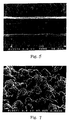
- FIG. 1 shows a microscopic photograph (5,000 times in magnification) of the matte surface of the electrolytic copper foil after the aforementioned buffing treatment. As seen from the microscopic photograph shown in FIG. 1, nodules formed of granular copper were electrodeposited along the fine concave/convex shape of the buff-treated surface.
- a corrosion prevention treatment was performed as follows on the matte surface side of the electrolytic copper foil which had been subjected to the aforementioned nodular forming treatment.
- a zinc-plating was performed for 8 seconds at a current density of 5 A/dm 2 using an electrolytic solution containing zinc at a concentration of 5 g/L and sulfuric acid at a concentration of 50 g/L and kept at a temperature of 25°C. Thereafter, an electrolytic chromating treatment was performed for 5 seconds at a current density of 1 A/dm 2 using an electrolytic solution containing chromic anhydride at a concentration of 2 g/L and adjusted in pH to 4. Subsequently, the resultant product was washed with running water and dried with hot air.
- the electrolytic copper foil obtained after these surface treatments was superimposed on one surface of a resin substrate made of fiberglass epoxy composite (FR-4) by means of a thermal press-bonding with this buffed surface of the copper foil being faced to the resin substrate, thereby obtaining a copper clad laminate board.
- FR-4 fiberglass epoxy composite
- a dry film (Nichigo Alfa Kabushiki Kaisha) was then superimposed on this copper clad laminate board, and exposed, via a pattern film bearing a resist width of 50 ⁇ m and a circuit interval of 100 ⁇ m, to a UV light, thereby forming a circuit pattern.
- the circuit pattern formed in this manner was then subjected to an etching at a temperature of 50°C for 30 seconds by using a copper chloride etching solution which is available in the market, thereby obtaining a printed wiring board bearing a desired wiring pattern.
- a piece of the printed wiring board was embedded in a cold embedding resin and kept for a whole day and night so as to allow the resin to be completely cured. Thereafter, a photograph of 1,500 times in magnification of the cross-section of the circuit pattern in the longitudinal direction thereof was taken by making use of a microscope (FIG. 2).
- the average value obtained was 0.48 and the standard deviation obtained was 0.43.
- the section of the circuit pattern becomes more close to a square in shape, i.e. more sharp in shape, the etching factor becomes larger in value.
- the etching factor obtained in Example 1 was 3.69 in average of six sectional pieces.
- a fiberglass epoxy composite substrate was press-bonded onto the buff-treated surface of the electrolytic copper foil obtained in Example 1 to manufacture a circuit pattern having a line width of 50 to 100 ⁇ m.
- This circuit pattern was then mounted on a sample table of an electron microscope and the microscopic photograph of 600 times in magnification of the circuit pattern (FIG. 5) was taken by making use of a field emission type electron microscope (Hitachi Seisakusho, S-4100). Since both surfaces of electrolytic copper foil obtained according to this invention was low in roughness, the linearity of the circuit was excellent. In this invention, the phenomenon that the quality of etching characteristics can be manifested by the features of the irregularity at the bottom line of the circuit was taken notice of, and therefore the etching characteristics was evaluated from the degree of irregularity as explained below.
- the peel strength of a wiring pattern with 10mm in line width was measured. As a result, the peel strength of the wiring pattern was found to be 1.02 kgf/cm.
- a granular copper layer was deposited on the matte surface side of an electrolytic copper foil with 18 ⁇ m in thickness, 1.60 ⁇ m in roughness (Rz) at the shiny side thereof, 4.60 ⁇ m in roughness (Rz) at the matte surface side thereof in the same conditions as explained in Example 1, but without performing the aforementioned buffing treatment.
- the surface roughness of the resultant matte surface side of the copper foil was found to be 5.75 ⁇ m.
- FIG. 7 shows a microscopic photograph (5,000 times in magnification) of the matte surface side of the electrolytic copper foil after the deposition of the granular copper.layer. As seen from FIG. 7, nodules formed of granular copper were irregularly electrodeposited on the matte surface side of the copper foil.
- the electrolytic copper foil obtained after these surface treatments was superimposed on one surface of a resin substrate made of fiberglass epoxy composite by means of a thermal press-bonding with this surface-treated side of the copper foil being faced to the resin substrate, thereby obtaining a copper clad laminate board.
- this copper clad laminate board was exposed, via a pattern film bearing a resist width of 50 ⁇ m and a circuit interval of 100 ⁇ m, to a UV light in the same manner as in Example 1, thereby forming a circuit pattern.
- the circuit pattern formed in this manner was then subjected to an etching to obtain a printed wiring board.
- the size of copper grains embedded in the fiberglass epoxy composite substrate was found to be 2.01 in average and the standard deviation was 1.67.
- the etching factor was found to be 1.86 in average of six sectional pieces.
- Example 2 a fiberglass epoxy composite substrate was press-bonded onto the treated surface of the electrolytic copper foil in the same manner as in Example 1 to manufacture a circuit pattern having a line width of 50 to 100 ⁇ m. Thereafter, the microscopic photograph of 600 times in magnification of this circuit pattern (FIG. 8 ) was taken in the same manner as in Example 1. As apparent from the microscopic photograph, since the matte surface side of electrolytic copper foil according to this Comparative Example 1 were high in roughness, the linearity of the circuit was poor.
- Example 2 a pair of parallel straight lines were drawn in the longitudinal direction of the circuit line in the same manner as in Example 1, and then the width of the bottom of the circuit was measured at 15 measuring points which were set apart equidistantly. Then, an average value and standard deviation of the measured widths were calculated.
- the peel strength of a wiring pattern with 10mm in line width was found to be 1.51 kgf/cm.
- a granular copper layer was deposited on the shiny side of the same electrolytic copper foil as employed in Example 1, i.e. 18 ⁇ m in thickness, 1.60 ⁇ m in roughness (Rz) at the shiny surface thereof, 2.50 ⁇ m in roughness (Rz) at the matte surface side thereof in the same conditions as explained in Example 1, but without performing the aforementioned buffing treatment.
- the surface roughness of the resultant shiny surface of the copper foil was found to be 2.09 ⁇ m.
- FIG. 9 shows a microscopic photograph (5,000 times in magnification) of the shiny side of the electrolytic copper foil after the deposition of the granular copper layer. As seen from FIG. 9, nodules formed of granular copper were irregularly electrodeposited on the shiny side of the copper foil.
- this electrolytic copper foil bearing a granular copper layer formed on the shiny surface thereof was exposed, via a pattern film bearing a resist width of 50 ⁇ m and a circuit interval of 100 ⁇ m, to a UV light in the same manner as in Example 1, thereby forming a circuit pattern.
- the circuit pattern formed in this manner was then subjected to an etching to obtain a printed wiring board.
- the size of copper grains embedded in the fiberglass epoxy composite substrate was found to be 0.98 in average and the standard deviation was 0.871.
- the etching factor was found to be 2.22 in average of six sectional pieces.
- a fiberglass epoxy composite substrate was press-bonded onto the treated surface of the electrolytic copper foil in the same manner as in Example 1 to manufacture a circuit pattern having a line width of from 50 to 100 ⁇ m.
- the microscopic photograph of 600 times in magnification of this circuit pattern was taken in the same manner as in Example 1. As apparent from the microscopic photograph, since the linearity of the circuit was not sufficient enough for use in the formation of an ultra-fine pattern.
- the peel strength of a wiring pattern with 10mm in line width was found to be 1.13 kgf/cm.
Landscapes
- Chemical & Material Sciences (AREA)
- Engineering & Computer Science (AREA)
- Chemical Kinetics & Catalysis (AREA)
- Materials Engineering (AREA)
- Metallurgy (AREA)
- Organic Chemistry (AREA)
- Electrochemistry (AREA)
- Microelectronics & Electronic Packaging (AREA)
- Manufacturing & Machinery (AREA)
- Inorganic Chemistry (AREA)
- Mechanical Engineering (AREA)
- Manufacturing Of Printed Wiring (AREA)
- Parts Printed On Printed Circuit Boards (AREA)
- Electroplating Methods And Accessories (AREA)
- Laminated Bodies (AREA)
- Manufacturing Of Printed Circuit Boards (AREA)
- ing And Chemical Polishing (AREA)
Claims (5)
- Eine elektrolytische Kupferfolie, in welcher ein ursprüngliches Profil einer matten Oberfläche davon vollständig beseitigt worden ist und feine Rauheiten mit polierten Streifen darauf neu gebildet worden sind, dadurch gekennzeichnet, dass eine Oberflächenrauigkeit Rz der matten Oberfläche vor der Bildung einer knollenförmigen Schicht 1,5 um oder kleiner ist und die Oberflächenrauigkeit davon nach der Bildung der knollenförmigen Schicht 1,5 bis 2,0 µm ist.
- Die elektrolytische Kupferfolie gemäß Anspruch 1, worin eine Korrosionsschutzschicht auf der knollenförmigen Schicht bereitgestellt wird.
- Die elektrolytische Kupferfolie gemäß Anspruch 2, worin die Korrosionsschutzschicht zusammengesetzt ist aus einer Zinkschicht und einer Chromatierschicht, die auf der Zinkschicht ausgebildet ist.
- Die elektrolytische Kupferfolie gemäß Anspruch 3, worin eine Silankopplungsschicht auf der Chromatierschicht ausgebildet ist.
- Ein Verfahren zur Herstellung einer elektrolytischen Kupferfolie zur Verwendung in einer Fertigung einer gedruckten Verdrahtungsplatte, welches die folgenden Schritte umfasst:Polieren einer matten Oberfläche der elektrolytischen Kupferfolie, um ein ursprüngliches Profil auf der matten Oberfläche vollständig zu beseitigen,weiter Polieren der vollständig beseitigten matten Oberfläche, um feine Rauheiten mit polierten Streifen neu zu bilden und um eine Oberflächenrauigkeit der matten Oberfläche vor der Bildung von Knollen darauf auf 1,5 µm oder weniger zu regulieren, undUnterwerfen dieser matten Oberfläche einer Knollenbildungsbehandlung, um die Oberflächenrauigkeit auf 1,5 bis 2,0 µm nach dieser Knollenbildungsbehandlung zu regulieren.
Applications Claiming Priority (3)
| Application Number | Priority Date | Filing Date | Title |
|---|---|---|---|
| JP2161896 | 1996-01-16 | ||
| JP02161896A JP3155920B2 (ja) | 1996-01-16 | 1996-01-16 | プリント配線板用電解銅箔及びその製造方法 |
| JP21618/96 | 1996-01-16 |
Publications (2)
| Publication Number | Publication Date |
|---|---|
| EP0785295A1 EP0785295A1 (de) | 1997-07-23 |
| EP0785295B1 true EP0785295B1 (de) | 2003-07-09 |
Family
ID=12060047
Family Applications (1)
| Application Number | Title | Priority Date | Filing Date |
|---|---|---|---|
| EP97100241A Expired - Lifetime EP0785295B1 (de) | 1996-01-16 | 1997-01-09 | Elektrolytische Kupferfolie für eine gedruckte Schaltungsplatte und verfahren zu ihrer Herstellung |
Country Status (8)
| Country | Link |
|---|---|
| US (2) | US5858517A (de) |
| EP (1) | EP0785295B1 (de) |
| JP (1) | JP3155920B2 (de) |
| KR (1) | KR100291856B1 (de) |
| CN (1) | CN1064414C (de) |
| DE (1) | DE69723327T2 (de) |
| MY (1) | MY117454A (de) |
| TW (1) | TW410533B (de) |
Cited By (1)
| Publication number | Priority date | Publication date | Assignee | Title |
|---|---|---|---|---|
| EP4455373A4 (de) * | 2021-12-22 | 2025-12-31 | Lotte Energy Mat Corporation | Oberflächenbehandelte kupferfolie mit hitzewiderstand, kupferkaschiertes laminat damit und leiterplatte |
Families Citing this family (44)
| Publication number | Priority date | Publication date | Assignee | Title |
|---|---|---|---|---|
| JP3476264B2 (ja) | 1993-12-24 | 2003-12-10 | 三井金属鉱業株式会社 | プリント回路内層用銅箔およびその製造方法 |
| DE19622429A1 (de) * | 1996-06-04 | 1997-12-11 | Wagner Int | Verfahren und Vorrichtung zum Bestimmen der Beschaffenheit einer Werkstückoberfläche |
| US6086743A (en) * | 1997-08-06 | 2000-07-11 | Gould Electronics, Inc. | Adhesion enhancement for metal foil |
| US6126761A (en) * | 1998-06-10 | 2000-10-03 | International Business Machines Corporation | Process of controlling grain growth in metal films |
| US6242078B1 (en) * | 1998-07-28 | 2001-06-05 | Isola Laminate Systems Corp. | High density printed circuit substrate and method of fabrication |
| JP3291482B2 (ja) * | 1999-08-31 | 2002-06-10 | 三井金属鉱業株式会社 | 整面電解銅箔、その製造方法および用途 |
| JP3291486B2 (ja) * | 1999-09-06 | 2002-06-10 | 三井金属鉱業株式会社 | 整面電解銅箔、その製造方法およびその用途 |
| US6372113B2 (en) * | 1999-09-13 | 2002-04-16 | Yates Foil Usa, Inc. | Copper foil and copper clad laminates for fabrication of multi-layer printed circuit boards and process for producing same |
| JP2001089892A (ja) * | 1999-09-21 | 2001-04-03 | Mitsui Mining & Smelting Co Ltd | キャリア箔付電解銅箔及びその製造方法並びにそのキャリア箔付電解銅箔を用いた銅張積層板 |
| JP2001177204A (ja) * | 1999-12-15 | 2001-06-29 | Mitsui Mining & Smelting Co Ltd | 表面処理銅箔及びその表面処理銅箔の製造方法 |
| JP3670186B2 (ja) * | 2000-01-28 | 2005-07-13 | 三井金属鉱業株式会社 | プリント配線板用表面処理銅箔の製造方法 |
| JP3661763B2 (ja) * | 2000-01-28 | 2005-06-22 | 三井金属鉱業株式会社 | プリント配線板用表面処理銅箔の製造方法 |
| JP3306404B2 (ja) * | 2000-01-28 | 2002-07-24 | 三井金属鉱業株式会社 | 表面処理銅箔の製造方法及びその製造方法で得られた表面処理銅箔を用いた銅張積層板 |
| JP3628585B2 (ja) * | 2000-04-05 | 2005-03-16 | 株式会社日鉱マテリアルズ | 銅張り積層板及び銅張り積層板のレーザーによる穴開け方法 |
| US20020182432A1 (en) * | 2000-04-05 | 2002-12-05 | Masaru Sakamoto | Laser hole drilling copper foil |
| JP2002105699A (ja) * | 2000-10-02 | 2002-04-10 | Nikko Materials Co Ltd | 銅張り積層板用電解銅箔及びその製造方法 |
| US7207008B1 (en) * | 2001-09-12 | 2007-04-17 | Bellsouth Intellectual Property Corp. | Method, system, apparatus, and computer-readable medium for interactive notification of events |
| US6770976B2 (en) | 2002-02-13 | 2004-08-03 | Nikko Materials Usa, Inc. | Process for manufacturing copper foil on a metal carrier substrate |
| US6596384B1 (en) | 2002-04-09 | 2003-07-22 | International Business Machines Corporation | Selectively roughening conductors for high frequency printed wiring boards |
| CN1301046C (zh) * | 2002-05-13 | 2007-02-14 | 三井金属鉱业株式会社 | 膜上芯片用软性印刷线路板 |
| TW200404484A (en) * | 2002-09-02 | 2004-03-16 | Furukawa Circuit Foil | Copper foil for soft circuit board package module, for plasma display, or for radio-frequency printed circuit board |
| TW200424359A (en) | 2003-02-04 | 2004-11-16 | Furukawa Circuit Foil | Copper foil for high frequency circuit, method of production and apparatus for production of same, and high frequency circuit using copper foil |
| JP5116943B2 (ja) * | 2003-02-04 | 2013-01-09 | 古河電気工業株式会社 | 高周波回路用銅箔及びその製造方法 |
| JP4226927B2 (ja) * | 2003-02-18 | 2009-02-18 | 三井金属鉱業株式会社 | キャパシタ層形成用の両面銅張積層板の製造方法 |
| JP3977790B2 (ja) * | 2003-09-01 | 2007-09-19 | 古河サーキットフォイル株式会社 | キャリア付き極薄銅箔の製造方法、及び該製造方法で製造された極薄銅箔、該極薄銅箔を使用したプリント配線板、多層プリント配線板、チップオンフィルム用配線基板 |
| US7190016B2 (en) * | 2004-10-08 | 2007-03-13 | Rohm And Haas Electronic Materials Llc | Capacitor structure |
| US7307022B2 (en) * | 2004-11-19 | 2007-12-11 | Endicott Interconnect Technologies, Inc. | Method of treating conductive layer for use in a circuitized substrate and method of making said substrate having said conductive layer as part thereof |
| US7383629B2 (en) * | 2004-11-19 | 2008-06-10 | Endicott Interconnect Technologies, Inc. | Method of making circuitized substrates utilizing smooth-sided conductive layers as part thereof |
| US6964884B1 (en) | 2004-11-19 | 2005-11-15 | Endicott Interconnect Technologies, Inc. | Circuitized substrates utilizing three smooth-sided conductive layers as part thereof, method of making same, and electrical assemblies and information handling systems utilizing same |
| JP4912909B2 (ja) * | 2006-03-30 | 2012-04-11 | 新日鐵化学株式会社 | フレキシブルプリント配線板の製造方法 |
| JP2008111188A (ja) * | 2007-09-25 | 2008-05-15 | Hitachi Chem Co Ltd | プリント配線板用の銅箔 |
| KR100974369B1 (ko) | 2008-02-29 | 2010-08-05 | 엘에스엠트론 주식회사 | 색상차와 내열 특성이 개선된 인쇄회로용 동박 |
| AT13462U1 (de) * | 2011-03-29 | 2013-12-15 | Austria Tech & System Tech | Verfahren zum herstellen, insbesondere bearbeiten oder bestücken, eines leiterplattenelements sowie träger zur verwendung in einem derartigen verfahren |
| JP5395854B2 (ja) * | 2011-08-11 | 2014-01-22 | タツタ電線株式会社 | プリント配線板及びプリント配線板の製造方法 |
| CN102618902B (zh) * | 2012-04-24 | 2015-04-01 | 山东金宝电子股份有限公司 | 一种挠性覆铜板用铜箔的表面处理工艺 |
| KR102038137B1 (ko) | 2012-12-21 | 2019-10-30 | 주식회사 넥스플렉스 | 다층 연성금속박 적층체 및 이의 제조방법 |
| KR20150025245A (ko) * | 2013-08-28 | 2015-03-10 | 삼성전기주식회사 | 인쇄회로기판용 동박 적층판 및 그의 제조방법 |
| JP2015134953A (ja) * | 2014-01-17 | 2015-07-27 | Jx日鉱日石金属株式会社 | 表面処理銅箔、キャリア付銅箔、プリント配線板、プリント回路板、銅張積層板及びプリント配線板の製造方法 |
| JP6178360B2 (ja) * | 2015-05-11 | 2017-08-09 | Jx金属株式会社 | 表面処理銅箔、キャリア付銅箔、プリント回路板の製造方法、銅張積層板の製造方法及びプリント配線板の製造方法 |
| CN109601024A (zh) * | 2017-07-31 | 2019-04-09 | 卢森堡电路箔片股份有限公司 | 表面处理过的铜箔和覆铜箔层压板 |
| CN108133886A (zh) * | 2017-12-11 | 2018-06-08 | 上海申和热磁电子有限公司 | 一种dbc基板背面研磨的方法 |
| DE112020003552T5 (de) * | 2019-07-26 | 2022-04-07 | Toyo Kohan Co., Ltd. | Aufgerautes nickelplattiertes Material und Verfahren zu dessen Herstellung |
| WO2023057067A1 (en) * | 2021-10-07 | 2023-04-13 | Circuit Foil Luxembourg | Copper foil with high engery at break and secondary battery comprising the same |
| CN114062076A (zh) * | 2021-11-04 | 2022-02-18 | 九江德福科技股份有限公司 | 一种用于铜箔晶体分析的样品制备方法 |
Family Cites Families (11)
| Publication number | Priority date | Publication date | Assignee | Title |
|---|---|---|---|---|
| JPS59136484A (ja) * | 1983-01-26 | 1984-08-06 | Fukuda Kinzoku Hakufun Kogyo Kk | 銅箔の粗面化処理方法 |
| JPS59145800A (ja) * | 1983-02-07 | 1984-08-21 | Fukuda Kinzoku Hakufun Kogyo Kk | 金属箔の粗面化処理方法 |
| US4961828A (en) * | 1989-04-05 | 1990-10-09 | Olin Corporation | Treatment of metal foil |
| JPH03236955A (ja) * | 1990-02-14 | 1991-10-22 | Shin Kobe Electric Mach Co Ltd | サーマルヘッド用金属箔張り積層板ならびにサーマルヘッド |
| JPH04202796A (ja) * | 1990-11-30 | 1992-07-23 | K D K Kk | プリント基板用銅箔及びその製造方法 |
| US5215646A (en) * | 1992-05-06 | 1993-06-01 | Circuit Foil Usa, Inc. | Low profile copper foil and process and apparatus for making bondable metal foils |
| JP2717911B2 (ja) * | 1992-11-19 | 1998-02-25 | 日鉱グールド・フォイル株式会社 | 印刷回路用銅箔及びその製造方法 |
| JPH06252548A (ja) * | 1993-02-24 | 1994-09-09 | Furukawa Electric Co Ltd:The | プリント配線基板用銅箔の表面処理方法と金属ベースプリント配線基板 |
| JP2762386B2 (ja) * | 1993-03-19 | 1998-06-04 | 三井金属鉱業株式会社 | 銅張り積層板およびプリント配線板 |
| US5545466A (en) * | 1993-03-19 | 1996-08-13 | Mitsui Mining & Smelting Co., Ltd. | Copper-clad laminate and printed wiring board |
| US5482784A (en) * | 1993-12-24 | 1996-01-09 | Mitsui Mining And Smelting Co., Ltd. | Printed circuit inner-layer copper foil and process for producing the same |
-
1996
- 1996-01-16 JP JP02161896A patent/JP3155920B2/ja not_active Expired - Lifetime
-
1997
- 1997-01-04 TW TW086100049A patent/TW410533B/zh not_active IP Right Cessation
- 1997-01-06 MY MYPI97000037A patent/MY117454A/en unknown
- 1997-01-09 DE DE69723327T patent/DE69723327T2/de not_active Expired - Fee Related
- 1997-01-09 EP EP97100241A patent/EP0785295B1/de not_active Expired - Lifetime
- 1997-01-14 CN CN97102226A patent/CN1064414C/zh not_active Expired - Fee Related
- 1997-01-15 US US08/783,575 patent/US5858517A/en not_active Expired - Fee Related
- 1997-01-16 KR KR1019970001147A patent/KR100291856B1/ko not_active Expired - Fee Related
-
1998
- 1998-07-24 US US09/122,526 patent/US5897761A/en not_active Expired - Lifetime
Cited By (1)
| Publication number | Priority date | Publication date | Assignee | Title |
|---|---|---|---|---|
| EP4455373A4 (de) * | 2021-12-22 | 2025-12-31 | Lotte Energy Mat Corporation | Oberflächenbehandelte kupferfolie mit hitzewiderstand, kupferkaschiertes laminat damit und leiterplatte |
Also Published As
| Publication number | Publication date |
|---|---|
| DE69723327D1 (de) | 2003-08-14 |
| JP3155920B2 (ja) | 2001-04-16 |
| DE69723327T2 (de) | 2004-07-22 |
| KR100291856B1 (ko) | 2001-06-01 |
| US5858517A (en) | 1999-01-12 |
| CN1064414C (zh) | 2001-04-11 |
| EP0785295A1 (de) | 1997-07-23 |
| KR970061019A (ko) | 1997-08-12 |
| MY117454A (en) | 2004-06-30 |
| CN1163318A (zh) | 1997-10-29 |
| TW410533B (en) | 2000-11-01 |
| JPH09195096A (ja) | 1997-07-29 |
| US5897761A (en) | 1999-04-27 |
Similar Documents
| Publication | Publication Date | Title |
|---|---|---|
| EP0785295A1 (de) | Elektrolytische Kupferfolie für eine gedruckte Schaltungsplatte und verfahren zu ihrer Herstellung | |
| US6984456B2 (en) | Flexible printed wiring board for chip-on flexibles | |
| JP4295800B2 (ja) | 電解銅箔 | |
| US5437914A (en) | Copper-clad laminate and printed wiring board | |
| KR100392173B1 (ko) | 가공된 표면을 가진 전해동박, 이의 제조방법, 및 이의 용도 | |
| JP3291482B2 (ja) | 整面電解銅箔、その製造方法および用途 | |
| EP1175132B1 (de) | Oberflächenbehandelte kupferfolie und ihre herstellungsmethode | |
| EP1511366A2 (de) | Verfahren zur Herstellung einer ultradünnen Kupferfolie mit Träger, so hergestellte ultradünne Kupferfolie mit Träger, Leiterplatte, mehrschichtige Leiterplatte und Chip-auf-Film-Leiterplatte | |
| JP2001068804A (ja) | キャリア箔付電解銅箔及びその電解銅箔の製造方法並びにその電解銅箔を使用した銅張積層板 | |
| JP3250994B2 (ja) | 電解銅箔 | |
| KR100437570B1 (ko) | 전해동박 및 그 물성 검사방법 및 그 전해동박을 사용한동 클래드 적층판 | |
| JPH10341066A (ja) | 印刷回路用銅箔、前記銅箔を用いた印刷回路用樹脂接着剤付銅箔、および前記銅箔を用いた印刷回路用銅張り積層板 | |
| JP2002506121A (ja) | 改良された光沢面を有する電解銅フォイル | |
| CN1076154C (zh) | 铜箔及采用该铜箔制作内层电路的高密度多层印刷电路板 | |
| JP4429539B2 (ja) | ファインパターン用電解銅箔 | |
| EP0250195A2 (de) | Kupferfolie mit einer matten Oberfläche auf beiden Seiten | |
| JPH09272994A (ja) | ファインパターン用電解銅箔 | |
| US9578739B2 (en) | Metal foil provided with electrically resistive layer, and board for printed circuit using said metal foil | |
| JP4330979B2 (ja) | 表面処理電解銅箔 | |
| JPWO1996025838A1 (ja) | 銅箔および該銅箔を内層回路用に用いた高密度多層プリント回路基板 | |
| KR20170001391A (ko) | 표면 처리 동박 및 그 제조방법 | |
| TW202244330A (zh) | 粗化處理銅箔、銅箔積層板及印刷佈線板 |
Legal Events
| Date | Code | Title | Description |
|---|---|---|---|
| PUAI | Public reference made under article 153(3) epc to a published international application that has entered the european phase |
Free format text: ORIGINAL CODE: 0009012 |
|
| AK | Designated contracting states |
Kind code of ref document: A1 Designated state(s): DE FR GB IT LU SE |
|
| 17P | Request for examination filed |
Effective date: 19970821 |
|
| 17Q | First examination report despatched |
Effective date: 20020920 |
|
| GRAH | Despatch of communication of intention to grant a patent |
Free format text: ORIGINAL CODE: EPIDOS IGRA |
|
| GRAH | Despatch of communication of intention to grant a patent |
Free format text: ORIGINAL CODE: EPIDOS IGRA |
|
| GRAA | (expected) grant |
Free format text: ORIGINAL CODE: 0009210 |
|
| AK | Designated contracting states |
Designated state(s): DE FR GB IT LU SE |
|
| PG25 | Lapsed in a contracting state [announced via postgrant information from national office to epo] |
Ref country code: IT Free format text: LAPSE BECAUSE OF FAILURE TO SUBMIT A TRANSLATION OF THE DESCRIPTION OR TO PAY THE FEE WITHIN THE PRE;WARNING: LAPSES OF ITALIAN PATENTS WITH EFFECTIVE DATE BEFORE 2007 MAY HAVE OCCURRED AT ANY TIME BEFORE 2007. THE CORRECT EFFECTIVE DATE MAY BE DIFFERENT FROM THE ONE RECORDED.SCRIBED TIME-LIMIT Effective date: 20030709 |
|
| REG | Reference to a national code |
Ref country code: GB Ref legal event code: FG4D |
|
| REF | Corresponds to: |
Ref document number: 69723327 Country of ref document: DE Date of ref document: 20030814 Kind code of ref document: P |
|
| PG25 | Lapsed in a contracting state [announced via postgrant information from national office to epo] |
Ref country code: SE Free format text: LAPSE BECAUSE OF FAILURE TO SUBMIT A TRANSLATION OF THE DESCRIPTION OR TO PAY THE FEE WITHIN THE PRESCRIBED TIME-LIMIT Effective date: 20031009 |
|
| ET | Fr: translation filed | ||
| PG25 | Lapsed in a contracting state [announced via postgrant information from national office to epo] |
Ref country code: LU Free format text: LAPSE BECAUSE OF NON-PAYMENT OF DUE FEES Effective date: 20040109 Ref country code: GB Free format text: LAPSE BECAUSE OF NON-PAYMENT OF DUE FEES Effective date: 20040109 |
|
| PLBE | No opposition filed within time limit |
Free format text: ORIGINAL CODE: 0009261 |
|
| STAA | Information on the status of an ep patent application or granted ep patent |
Free format text: STATUS: NO OPPOSITION FILED WITHIN TIME LIMIT |
|
| 26N | No opposition filed |
Effective date: 20040414 |
|
| PG25 | Lapsed in a contracting state [announced via postgrant information from national office to epo] |
Ref country code: DE Free format text: LAPSE BECAUSE OF NON-PAYMENT OF DUE FEES Effective date: 20040803 |
|
| GBPC | Gb: european patent ceased through non-payment of renewal fee |
Effective date: 20040109 |
|
| PG25 | Lapsed in a contracting state [announced via postgrant information from national office to epo] |
Ref country code: FR Free format text: LAPSE BECAUSE OF NON-PAYMENT OF DUE FEES Effective date: 20040930 |
|
| REG | Reference to a national code |
Ref country code: FR Ref legal event code: ST |