EP0686960A2 - Dispositif d'affichage et méthode de commande - Google Patents
Dispositif d'affichage et méthode de commande Download PDFInfo
- Publication number
- EP0686960A2 EP0686960A2 EP95303872A EP95303872A EP0686960A2 EP 0686960 A2 EP0686960 A2 EP 0686960A2 EP 95303872 A EP95303872 A EP 95303872A EP 95303872 A EP95303872 A EP 95303872A EP 0686960 A2 EP0686960 A2 EP 0686960A2
- Authority
- EP
- European Patent Office
- Prior art keywords
- image signal
- display according
- row
- rows
- signal
- Prior art date
- Legal status (The legal status is an assumption and is not a legal conclusion. Google has not performed a legal analysis and makes no representation as to the accuracy of the status listed.)
- Granted
Links
Images


Classifications
-
- G—PHYSICS
- G09—EDUCATION; CRYPTOGRAPHY; DISPLAY; ADVERTISING; SEALS
- G09G—ARRANGEMENTS OR CIRCUITS FOR CONTROL OF INDICATING DEVICES USING STATIC MEANS TO PRESENT VARIABLE INFORMATION
- G09G3/00—Control arrangements or circuits, of interest only in connection with visual indicators other than cathode-ray tubes
- G09G3/20—Control arrangements or circuits, of interest only in connection with visual indicators other than cathode-ray tubes for presentation of an assembly of a number of characters, e.g. a page, by composing the assembly by combination of individual elements arranged in a matrix no fixed position being assigned to or needed to be assigned to the individual characters or partial characters
- G09G3/34—Control arrangements or circuits, of interest only in connection with visual indicators other than cathode-ray tubes for presentation of an assembly of a number of characters, e.g. a page, by composing the assembly by combination of individual elements arranged in a matrix no fixed position being assigned to or needed to be assigned to the individual characters or partial characters by control of light from an independent source
- G09G3/36—Control arrangements or circuits, of interest only in connection with visual indicators other than cathode-ray tubes for presentation of an assembly of a number of characters, e.g. a page, by composing the assembly by combination of individual elements arranged in a matrix no fixed position being assigned to or needed to be assigned to the individual characters or partial characters by control of light from an independent source using liquid crystals
- G09G3/3611—Control of matrices with row and column drivers
-
- G—PHYSICS
- G09—EDUCATION; CRYPTOGRAPHY; DISPLAY; ADVERTISING; SEALS
- G09G—ARRANGEMENTS OR CIRCUITS FOR CONTROL OF INDICATING DEVICES USING STATIC MEANS TO PRESENT VARIABLE INFORMATION
- G09G3/00—Control arrangements or circuits, of interest only in connection with visual indicators other than cathode-ray tubes
- G09G3/20—Control arrangements or circuits, of interest only in connection with visual indicators other than cathode-ray tubes for presentation of an assembly of a number of characters, e.g. a page, by composing the assembly by combination of individual elements arranged in a matrix no fixed position being assigned to or needed to be assigned to the individual characters or partial characters
- G09G3/34—Control arrangements or circuits, of interest only in connection with visual indicators other than cathode-ray tubes for presentation of an assembly of a number of characters, e.g. a page, by composing the assembly by combination of individual elements arranged in a matrix no fixed position being assigned to or needed to be assigned to the individual characters or partial characters by control of light from an independent source
- G09G3/36—Control arrangements or circuits, of interest only in connection with visual indicators other than cathode-ray tubes for presentation of an assembly of a number of characters, e.g. a page, by composing the assembly by combination of individual elements arranged in a matrix no fixed position being assigned to or needed to be assigned to the individual characters or partial characters by control of light from an independent source using liquid crystals
- G09G3/3611—Control of matrices with row and column drivers
- G09G3/3674—Details of drivers for scan electrodes
- G09G3/3677—Details of drivers for scan electrodes suitable for active matrices only
-
- G—PHYSICS
- G09—EDUCATION; CRYPTOGRAPHY; DISPLAY; ADVERTISING; SEALS
- G09G—ARRANGEMENTS OR CIRCUITS FOR CONTROL OF INDICATING DEVICES USING STATIC MEANS TO PRESENT VARIABLE INFORMATION
- G09G3/00—Control arrangements or circuits, of interest only in connection with visual indicators other than cathode-ray tubes
- G09G3/20—Control arrangements or circuits, of interest only in connection with visual indicators other than cathode-ray tubes for presentation of an assembly of a number of characters, e.g. a page, by composing the assembly by combination of individual elements arranged in a matrix no fixed position being assigned to or needed to be assigned to the individual characters or partial characters
- G09G3/34—Control arrangements or circuits, of interest only in connection with visual indicators other than cathode-ray tubes for presentation of an assembly of a number of characters, e.g. a page, by composing the assembly by combination of individual elements arranged in a matrix no fixed position being assigned to or needed to be assigned to the individual characters or partial characters by control of light from an independent source
- G09G3/36—Control arrangements or circuits, of interest only in connection with visual indicators other than cathode-ray tubes for presentation of an assembly of a number of characters, e.g. a page, by composing the assembly by combination of individual elements arranged in a matrix no fixed position being assigned to or needed to be assigned to the individual characters or partial characters by control of light from an independent source using liquid crystals
- G09G3/3611—Control of matrices with row and column drivers
- G09G3/3685—Details of drivers for data electrodes
- G09G3/3688—Details of drivers for data electrodes suitable for active matrices only
-
- G—PHYSICS
- G09—EDUCATION; CRYPTOGRAPHY; DISPLAY; ADVERTISING; SEALS
- G09G—ARRANGEMENTS OR CIRCUITS FOR CONTROL OF INDICATING DEVICES USING STATIC MEANS TO PRESENT VARIABLE INFORMATION
- G09G2310/00—Command of the display device
- G09G2310/02—Addressing, scanning or driving the display screen or processing steps related thereto
- G09G2310/0202—Addressing of scan or signal lines
- G09G2310/0205—Simultaneous scanning of several lines in flat panels
-
- G—PHYSICS
- G09—EDUCATION; CRYPTOGRAPHY; DISPLAY; ADVERTISING; SEALS
- G09G—ARRANGEMENTS OR CIRCUITS FOR CONTROL OF INDICATING DEVICES USING STATIC MEANS TO PRESENT VARIABLE INFORMATION
- G09G2310/00—Command of the display device
- G09G2310/02—Addressing, scanning or driving the display screen or processing steps related thereto
- G09G2310/0243—Details of the generation of driving signals
- G09G2310/0251—Precharge or discharge of pixel before applying new pixel voltage
-
- G—PHYSICS
- G09—EDUCATION; CRYPTOGRAPHY; DISPLAY; ADVERTISING; SEALS
- G09G—ARRANGEMENTS OR CIRCUITS FOR CONTROL OF INDICATING DEVICES USING STATIC MEANS TO PRESENT VARIABLE INFORMATION
- G09G2310/00—Command of the display device
- G09G2310/02—Addressing, scanning or driving the display screen or processing steps related thereto
- G09G2310/0264—Details of driving circuits
- G09G2310/0297—Special arrangements with multiplexing or demultiplexing of display data in the drivers for data electrodes, in a pre-processing circuitry delivering display data to said drivers or in the matrix panel, e.g. multiplexing plural data signals to one D/A converter or demultiplexing the D/A converter output to multiple columns
-
- G—PHYSICS
- G09—EDUCATION; CRYPTOGRAPHY; DISPLAY; ADVERTISING; SEALS
- G09G—ARRANGEMENTS OR CIRCUITS FOR CONTROL OF INDICATING DEVICES USING STATIC MEANS TO PRESENT VARIABLE INFORMATION
- G09G2340/00—Aspects of display data processing
- G09G2340/04—Changes in size, position or resolution of an image
- G09G2340/0407—Resolution change, inclusive of the use of different resolutions for different screen areas
- G09G2340/0414—Vertical resolution change
-
- G—PHYSICS
- G09—EDUCATION; CRYPTOGRAPHY; DISPLAY; ADVERTISING; SEALS
- G09G—ARRANGEMENTS OR CIRCUITS FOR CONTROL OF INDICATING DEVICES USING STATIC MEANS TO PRESENT VARIABLE INFORMATION
- G09G3/00—Control arrangements or circuits, of interest only in connection with visual indicators other than cathode-ray tubes
- G09G3/20—Control arrangements or circuits, of interest only in connection with visual indicators other than cathode-ray tubes for presentation of an assembly of a number of characters, e.g. a page, by composing the assembly by combination of individual elements arranged in a matrix no fixed position being assigned to or needed to be assigned to the individual characters or partial characters
- G09G3/2007—Display of intermediate tones
- G09G3/2011—Display of intermediate tones by amplitude modulation
-
- G—PHYSICS
- G09—EDUCATION; CRYPTOGRAPHY; DISPLAY; ADVERTISING; SEALS
- G09G—ARRANGEMENTS OR CIRCUITS FOR CONTROL OF INDICATING DEVICES USING STATIC MEANS TO PRESENT VARIABLE INFORMATION
- G09G3/00—Control arrangements or circuits, of interest only in connection with visual indicators other than cathode-ray tubes
- G09G3/20—Control arrangements or circuits, of interest only in connection with visual indicators other than cathode-ray tubes for presentation of an assembly of a number of characters, e.g. a page, by composing the assembly by combination of individual elements arranged in a matrix no fixed position being assigned to or needed to be assigned to the individual characters or partial characters
- G09G3/2092—Details of a display terminals using a flat panel, the details relating to the control arrangement of the display terminal and to the interfaces thereto
-
- G—PHYSICS
- G09—EDUCATION; CRYPTOGRAPHY; DISPLAY; ADVERTISING; SEALS
- G09G—ARRANGEMENTS OR CIRCUITS FOR CONTROL OF INDICATING DEVICES USING STATIC MEANS TO PRESENT VARIABLE INFORMATION
- G09G3/00—Control arrangements or circuits, of interest only in connection with visual indicators other than cathode-ray tubes
- G09G3/20—Control arrangements or circuits, of interest only in connection with visual indicators other than cathode-ray tubes for presentation of an assembly of a number of characters, e.g. a page, by composing the assembly by combination of individual elements arranged in a matrix no fixed position being assigned to or needed to be assigned to the individual characters or partial characters
- G09G3/22—Control arrangements or circuits, of interest only in connection with visual indicators other than cathode-ray tubes for presentation of an assembly of a number of characters, e.g. a page, by composing the assembly by combination of individual elements arranged in a matrix no fixed position being assigned to or needed to be assigned to the individual characters or partial characters using controlled light sources
Definitions
- the present invention relates to a display and its driving method, and more particularly to a display and its driving method for inputting the image signal of various standards into the panel having only a predefined number of rows.
- a thin type flat display as the computer to human interface, in place of CRT (Cathode Ray Tube), becomes an important device to extend the multi-media market.
- CRT Cathode Ray Tube
- the liquid crystal display has gained large market along with the spread of small-sized personal computers.
- an active matrix liquid crystal display has greater contrast over the whole screen because of having no crosstalk, as compared with a simple matrix liquid crystal display such as STN. Therefore, the active matrix liquid crystal display has drawn public's attention not only as the display for small personal computers, but also as the view finder for video camera, the projector, and the thin type television.
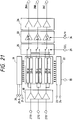
- Fig. 33A is a block diagram of the image signal input for TFT image display.
- 20 is a display pixel unit having pixels arranged in a matrix
- 40 is a vertical scan circuit for selecting the display row
- 30 is a sampling circuit for color image signal
- 80 is a horizontal scan circuit for outputting the sampling signal.
- a unit pixel of the display pixel unit 20 is composed of a switching element 11, a liquid crystal material 15, and a pixel capacitor 12.
- the switching element 11 is a TFT (thin film transistor)
- a gate line 13 connects the gate electrode of TFT to the vertical scan circuit 40, one terminal of pixel capacitor 12 for each of all the pixels being connected commonly to a common electrode 21 of an opposed substrate, to which a common electrode voltage V LC is applied.
- the switching element 11 is a diode (including Metal/Insulator/Metal element)
- the scan electrode runs transversely across the opposed substrate to connect to the vertical scan circuit 20.
- An input terminal of the switching element 11 is connected by a vertical data line to the sampling circuit 30.
- a vertical data line 14 connects the input terminal of the switching element 14 to the sampling circuit 30, and an output terminal of the switching element 14 is connected to the other terminal of the pixel capacitor 12.
- a control circuit 140 separates an image signal into necessary signals for the vertical scan circuit 40, the horizontal scan circuit 80 or a signal processing circuit 120.
- the signal processing circuit 120 performs a gamma processing in view of the liquid crystal characteristics, or an inversion signal processing for the longer life of liquid crystal to output a color image signal (red, blue, green) to the sampling circuit 30.
- Fig. 33B is a detail equivalent circuit diagram of the display pixel unit 20 and the sampling circuit 30 for TFT color.
- 10 is a unit pixel for each color.
- the pixels (R, G, B) are arranged in delta configuration, the same color being allocated on either side of the data line 14 (d1, d2,%) for every row, and connected to the data line 14 (d1, d2,).
- the sampling circuit 30 is comprised of switching transistors (sw1, sw2,...) and capacitors (parasitic capacitor and pixel capacitor of the data line 14).
- An image signal input line 16 is comprised of a signal line dedicated for each color of RGB.
- the switching transistors (sw1, sw2,%) sample each color signal from the image signal input line 16 in accordance with a pulse ( ⁇ h1, ⁇ h2,%) from the horizontal scan circuit 80, and transfer each color signal to each pixel through the data line 14 (d1, d2,). And they send pulses ( ⁇ g1, ⁇ g2,%) from the vertical scan circuit 40 to the TFT gate of pixels, and write a signal into each pixel by selecting the row.
- the pulse ( ⁇ g1, ⁇ g2,%) turns on the TFT 11 contained in each row, so that the image signal for one horizontal scan in each corresponding row is written into all pixels contained in each row. It is noted that the image signal for one horizontal scan is thereafter referred to as 1H signal.
- the liquid crystal display displays a television signal or a personal computer signal, but there are a variety of standards for these signals, whereby it is necessary to normally fabricate the panel for liquid crystal display of the type conforming to respective standard.
- a liquid crystal display for displaying the signal of various standards on one panel through an appropriate signal processing.
- a liquid crystal display is provided which displays the image of PAL (Phase Alternation by Line) system having more scan lines than the NTSC (National Television System Committee) system on the panel only having the rows corresponding to the number of scan lines in the NTSC system.
- PAL Phase Alternation by Line
- NTSC National Television System Committee
- a processing of thinning out some 1H signals from the image signal according to the PAL system is adopted. Specifically, in order to transform the effective number of scan lines 280 for one field in the PAL system into 240 lines of the NTSC system, the image signal is thinned out at a rate of 1 line for every 7 lines.
- Fig. 9 represents a specific example of this thinning out method.
- the image signal of PAL system is written on a liquid crystal display only having the rows for one field (i.e., half rows of one frame) of the NTSC system. If the image signal of NTSC system is input, 1H signal o1, o2,... for odd field, or 1H signal e1, e2,...
- the image signal when the image signal is input into the liquid crystal display, it is common that the image signal is made the alternating current to prevent the burning of liquid crystal material.
- the central voltage is preferably 0. Namely, it is preferable that adjacent rows are reversely polarized, and the polarity in the same row is reversed in a short time. This is true with a plasma display and an electron beam flat display in which if deflected signal voltage is input for long time, the electrode is corroded and the element is deteriorated. In this respect, because Japanese Laid-Open Patent Application No.
- the present invention has a subject to provide a display capable of displaying the image signal of various standards while reducing image distortion associated with the scan for thinning out as much as possible, thereby inputting reversely the image signal optimally, only with the addition of a simple circuit.
- a display according to the present invention has a plurality of pixels arranged in a matrix, having a panel with the number of rows being m, and writing on said m rows the image signal constituting one field by the k horizontal scans (k ⁇ m and k ⁇ m/2 ), while sequentially selecting the row, characterized by comprising vertical scan altering means for writing all the image signal corresponding to said k horizontal scans into respective rows of said m rows, within one field, and altering the number of rows to write the image signal corresponding to any horizontal scan.
- the present invention encompasses an invention of the driving method of display.
- a driving method for a display according to the present invention having a plurality of pixels arranged in a matrix, and having a panel with the number of rows being m, includes writing on the m rows the image signal constituting one field by the k horizontal scans (k ⁇ m and k ⁇ m/2 ), while sequentially selecting the row, characterized in that vertical scan altering means writes all the image signal corresponding to said k horizontal scans into respective rows of said m rows, within one field, and alters the number of rows to write the image signal corresponding to any horizontal scan.
- Fig. 1 shows an interlace circuit which is a portion of vertical scan altering means according to the present invention.
- 1 is a first control line
- 2 is a second control line
- 3 is a third control line
- 1-1, 1-2, 1-3 is a first group of switches
- 2-1, 2-2, 2-3 is a second group of switches
- 3-1, 3-2, 3-3 is a third group of switches.
- m1, m3, m5 is a line leading to a vertical scan circuit.
- the vertical scan circuit should be a bootstrap scan circuit. If the image signal constituting one frame by m horizontal scans is of the NTSC system, m is from 480 to 525. If the image signal constituting one field by k (k, m) horizontal scans to input the image is of the PAL system, k is from 250 to 313. Image signal input means normally writes the image signal corresponding to one horizontal scan, among k horizontal scans as above cited, into two rows, and only at every arbitrary n-th (n ⁇ k) horizontal scan, writes the image signal corresponding to said n-th horizontal scan into any one row among said m rows. This value of n is desirably from 2 to 8, and more desirably from 3 to 4.
- the present invention is not limited to the NTSC system or PAL system, but also deal with the image signal of various standards.
- VGA Video Graphic Array; the number of rows 480
- SVGA Super Video Graphic Array; the number of rows 600
- XGA Extended Graphics Array; the number of rows 768)
- EWS Engineing Work Station; the number of rows 1024
- the present invention can deal with any display as far as it is of the type sequentially scanning a multiplicity of rows by a scan circuit.
- Examples of the display of such type include a liquid crystal display, a plasma display, an electron beam flat display, an electroluminescence display and a multiluminous diode display.
- the present invention has a significant advantage over the small-sized portable display because of the capability of displaying the image signal of various standards.
- these liquid crystal display, plasma display, and electron beam display it is a liquid crystal display that is most portable, and it is most beneficial to apply the present invention to the liquid crystal display.
- This liquid crystal display is either of the active matrix type and the simple matrix type.
- an active matrix type liquid crystal display that allows the interpolation driving of multiple rows, for one data line, while connecting a plurality of pixels that are offset in the horizontal direction due to delta arrangement.
- an example 1 as hereinafter described is illustrative thereof.
- a two-row simultaneous driving may be applied to both the simple matrix and the active matrix.
- the active matrix type liquid crystal display may be of two terminal type (MIM type), or three terminal type (TFT type).
- 1H signal is displayed in multiple rows (the number of simultaneously selected rows is assumed p), but some 1H signal is displayed only in q ( ⁇ p) rows when displayed. Especially, 1H signal is written into two rows, but certain 1H signal is written in only one row. Hence, even if the signal having necessary more rows as with the PAL system is input into a display only having less rows as with the NTSC system, there is no 1H signal to completely thin out. In this way, a display manufactured in the NTSC system can be made a display in the PAL system, and a display manufactured for the PAL can be made a display for the NTSC system. Therefore, it is possible to display the image signal of various standards on a single display. Also, the inversion input of image signal optimal for the panel can be effected only by the addition of a simple circuit.
- Fig. 1 shows an example of vertical scan altering means of the present invention.
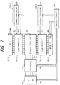
- Fig. 2 is a block diagram showing the flow of image signal in an example 1.
- Fig. 3 is a detail view of an interlace circuit and a line memory.
- Fig. 4 is a chart showing the phase and polarity of image signal for each row on a panel.
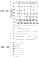
- Figs. 5A and 5B are examples of the timing chart.
- Figs. 6A and 6B are examples of the timing chart.
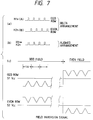
- Fig. 7 represents (a) sampling pulse in delta arrangement, (b) sampling pulse in aligned arrangement, and (c) inversion image signal.
- Figs. 8A and 8B represent circuit diagram and voltage waveform for a bootstrap scan circuit.
- Fig. 9 represents the voltage waveform generating the scan pulse.
- Fig. 10 is a chart showing the phase and polarity of image signal for each row on a panel in an example 2.
- Fig. 11 is a chart showing the phase and polarity of image signal for each row on a panel in an example 3.
- Fig. 12 is a diagram showing a pixel array in an example 4.
- Fig. 13 shows exemplary timing charts.
- Figs. 14A and 14B represent a block diagram showing the flow of image signal in examples 6, 7, 8 and a detail diagram of a display unit.
- Fig. 15 is a diagram showing the input of image signal.
- Fig. 16 is a view showing the color array of pixel.
- Fig. 17 shows exemplary timing charts.
- Fig. 18 is a chart showing the image signal for each row on a panel in an example 6.
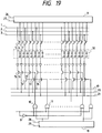
- Fig. 19 is a diagram showing the input of image signal.
- Fig. 20 is a view showing the color array of pixel.
- Fig. 21 is a block diagram of an analog line memory.
- Fig. 22 shows exemplary timing charts.
- Fig. 23 is a chart showing the image signal for each row on a panel in an example 7.
- Fig. 24 shows exemplary timing charts.
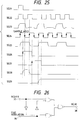
- Fig. 25 shows exemplary timing charts.
- Fig. 26 shows an example of a circuit for phasing image signal.
- Fig. 27 shows exemplary timing charts.
- Fig. 28 is a chart showing the input of image signal.
- Fig. 29 is a block diagram of an analog line memory.
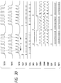
- Fig. 30 shows exemplary timing charts.
- Figs. 31A and 31B are typical views of an original signal image and an image in an example 8.
- Fig. 32 is a view showing an electron beam flat display.
- Figs. 33A and 33B are block diagrams of the conventional flow of image signal and a detail diagram of pixel.
- Fig. 34 is a chart showing the polarity of image signal for each row on a conventional panel.
- FIG. 1 is one in which the present invention is applied to the two-row interpolation driving which is effective for the pixels in delta arrangement.
- the two-row interpolation driving has two image input circuits.
- Fig. 2 is a block diagram showing the flow of image signal in this example.
- 20 is a display pixel unit
- 40 is a vertical scan circuit of the display pixel unit
- 60 is an interlace circuit for row selection
- 80-1, 80-2 are horizontal scan circuits for display pixel unit
- 100-1, 100-2 are line memories for temporarily storing the image signal sampled
- 120-1, 120-2 are signal processing circuits for gamma processing of image signal of inversion signal processing for electrical polarity to drive the liquid crystal
- 140 is a control circuit for driving the display device.
- S1 and S2 represent image signals which have undergone signal processing in different signal processing circuits 120-1, 120-2, respectively.
- the first image input circuit contains 80-1, 100-1, 120-1
- the second image input circuit contains 80-2, 100-2, 120-2.
- Fig. 3 is a detail circuit diagram of the interlace circuit 60, the display pixel unit 20, and the line memories 100-1, 100-2.
- 10 is a unit pixel consisting of a switching element, a liquid crystal and a color filter
- D1 to D n are vertical signal lines (data lines)
- V1 to V2 are signal lines from the vertical scan circuit
- L1 to L n are horizontal gate lines for the row selection.
- 17 is a reset transistor
- 18 is a temporary storage capacitor
- 19 is a switching transistor.
- the interlace circuit allows for various drivings including the interlace, two-line simultaneous field row shift, and non-interlace.
- Fig. 4 is a chart showing the image signal to be written into the pixel in the example 1.
- the panel row is indicated by L1, L2, ...
- the image signal to be written into corresponding row is indicated by o1, o2, ... in the odd field and e1, e2, ... in the even field for every 1H.
- the sampling phase of the signal to be written in each row pixel is indicated by A and B
- the inversion signal polarity is indicated by - and +. This sampling phase indicates a difference in the sampling timing.
- Fig. 7 represents the sampling pulse from the shift register (80-1, 80-2) in (a) delta arrangement and (b) aligned arrangement.
- each 1H signal is alternately written by changing the sampling phase (e.g., a signal o1 at 1H is written on a row L1 as o1A-, and on a row L2 as o1B+).
- a signal o3 at 3H is written on a row pixel L5 as o3A-
- the other is not written (o3B+).
- the not written image signal is indicated by ⁇ .
- the image in the vertical direction is compressed.
- the vertical resolution is not degraded.
- the next 4H signal is written as o4B+ on a row L6 and o4A- on a row L7 by the interlace circuit.
- Such normal driving and compression driving operation is performed for every several Hs in both the odd field and the even field.
- Figs. 5A and 5B represent the timing charts in this example.
- Fig. 5B is an enlarged chart of a portion surrounded by the dot line in Fig. 5A.
- (c) in Fig. 7 represents signal waveform examples of inversion image of a pixel.
- a phase, negative polarity signal is temporarily stored in the line memory 1
- B phase, positive polarity signal is temporarily stored in the line memory 2, these signals being then transferred to each row.
- ⁇ H is a horizontal blanking pulse
- ⁇ c is a residual charge reset pulse for selected pixel and vertical signal line
- ⁇ Go, ⁇ Ge, ⁇ G are interlace pulses
- V1, V2,.. are vertical scan pulses.
- the horizontal blanking pulse represents the synchronizing signal for the image signal.
- ⁇ T1 is a transfer pulse from the line memory (100-1) to selected row
- ⁇ T2 is a transfer pulse from the line memory 2 (100-2) to selected row.
- the interlace pulses V1, V2 represent selected rows at 1H and 2H.
- the image signal o1 is sampled in the line memory 1 and the line memory 2 during its effective scan period.
- the sampling timing id different in sampling phase between odd row and even row of row pixel, as shown (a) in Fig. 7.
- an image signal is written from the row L6 into which no signal is written at 3H. since the selection of row L6 is performed by a ⁇ Ge pulse, the V3 pulse remains "H" at 4H, continuing from 3H.
- the row L6 is selected by ⁇ Ge pulse, and the row L7 is selected by a ⁇ G pulse but not by a ⁇ Go. In this way, for every compression driving of image, the selection of row is switched by a drive pulse of the interlace circuit. Also, by inputting a pulse as shown in Figs. 6A and 6B, the same display can be effected.
- a vertical scan circuit of this example will be detailed below.
- Fig. 8A is a partial circuit diagram of a bootstrap scan circuit in this example
- Fig. 8B is a voltage waveform chart of each portion to present the operation of this example.
- the vertical scan circuit is of a construction of having n unit circuits connected, in which a scan pulse ⁇ 1 to ⁇ n is sequentially output from each unit circuit. Note that the potential of each portion in Fig. 8A is indicated such as V(1) using the number attached to each portion.
- a transistor M1 conducts to cause the potential V(4) to increase. Since the potential V(4) is a gate potential of a transistor M2, the transistor M2 indicates a conductance corresponding to the potential V(4).
- the pulse ⁇ v1 falls and the pulse ⁇ v2 rises, the potential V(5) increases through the transistor M2.
- the increase in the potential V(5) is fed back to the gate of the transistor M2 through a capacitor C1, to cause the potential V(4) to increase due to a bootstrap effect. Since the increase in the potential V(4) acts to increase the conductance of transistor M2, the pulse ⁇ v2 passes without substantial voltage drop due to transistor M2 to cause the potential V(5) to increase through a transistor M3.
- the conductance of transistor M5 rises correspondingly to the potential V(6).
- the pulse ⁇ v1 rises, the potential V(7) increases through a transistor M6. Owing to the bootstrap effect as above mentioned, the potential V(6) further increases along with the increase in the potential V(7). Since the increase in the potential V(6) acts to raise the conductance of transistor M5, the pulse ⁇ v1 causes the potential V(5) to increase through transistors M6 and M7 (see Fig. 8B). Accordingly, a transistor M10 indicates a conductance corresponding to the gate potential V(5).
- the potential V(8) is reset by the pulse ⁇ v1, and at the same time the potential V(12) increases, so that the potential further increase by a pulse that follows.
- This potential V(12) is utilized as the scan pulse ⁇ 2.
- high voltage scan pulses ⁇ 3 to ⁇ n are sequentially output in synchronization with the pulse ⁇ v2.
- the waveform for the scan pulses ⁇ 1 to ⁇ n can be closer to the rectangle.
- the vertical scan circuit In order to cause the vertical scan circuit to output a long pulse, such as V(3) shown in Figs. 5A and 6B, the pulses such as ⁇ v1 and ⁇ v2 of Fig. 9 are input into the vertical scan circuit.
- the sampling phase is out of phase by 180° as shown in (a) in Fig. 7, but it will be appreciated that in the aligned arrangement, the image signal is in identical phase for sampling on both rows as shown in (b) in Fig. 7, because two rows are sampled at the same timing.
- a logic circuit with CMOS can be available.
- the image signal having different sampling phase and different signal polarity was written in field inversion into each row by two-row interpolation driving.
- a first image input circuit and a second image input circuit changes the sampling phase of image signal for every 1H.
- the display is a TFT type liquid crystal display as described in Fig. 1.
- the signal processing circuits 120-1, 120-2 of Fig. 1 are inverted for every 1H to output signals S1, S2 which are opposite in the signal polarity.
- Fig. 10 is a chart representing the sampling phase and the signal polarity correspondingly to each row. The meaning "A" and "B" and “+” and "-" is the same as in the example 1.
- the inversion operation which the signal processing circuits 120-1, 120-2 perform is to always invert the image signal for every 1H, the direct current potential control feedback time constant is smaller. Hence, the rising at the power on is faster, so that the integrating capacity can be reduced.
- An example 3 is one in which the signal polarity is inverted for every two rows on the display.
- the display is a TFT type liquid crystal display as in the example 1 and shown in Fig. 1. It is not necessary to change the phase in sampling because of the same sampling phase of input signal into the line memories 1, 2 as in the example 1.
- Fig. 11 is a chart representing the sampling phase and the signal polarity correspondingly to each row. The meaning "A" and "B" and “+” and “-” are the same as in the example 1.
- the signal polarity is basically inverted for every 1H, but when the image signal is compressed and written in one row, the inversion operation is temporarily stopped.
- the number of rows for the display in an example 4 is the same as the number of scan lines for the NTSC signal, wherein the connection to each pixel occurs at every other row.
- the display is an active matrix type or a simple matrix type liquid crystal display.
- Fig. 12 represents a liquid crystal display of this example. Since the image signal is directly written in each row during the horizontal effective scan period, no line memory is necessary. Also in this example, there is an interlace circuits for the wirings of rows (L1, L2,%) identical to that of the example 1 as shown in Fig. 2.
- Fig. 13 is the timing chart of this example.
- the number of rows for the display in an example 5 is the same as the number of scan lines for the NTSC signal, wherein two-row simultaneous driving is made.
- the display is an active matrix type or a simple matrix type liquid crystal display having the pixels arranged in aligned lattice.
- the signal to be written in two rows selected simultaneously is sampled at the same timing, as described in (b) in Fig. 7. And because of the use of an interlace circuit as shown in Fig. 1, there is less image distortion with the PAL signal having more scan lines than the NTSC signal. In this example, the level of signal S1 and that of signal S2 are the same. Also, the row shift driving to change the row combination between the odd field and the even field is conducted.
- the signal S1 may be original image signal
- the signal S2 may be the average of original image signal at selected row and image signal at the next row.
- odd1 signal is written in the rows L2 and L3 during 1H period
- original image signal odd1 is written in the row L2
- an average signal ( (odd1+odd2)/2 ) of signal odd2 and signal odd1 during 2H period as prefetched is written in the row L3.
- the same row combinations may be used for the odd field and the even field.
- Fig. 14A shows the system configuration of a liquid crystal display unit in the present invention.
- 1 is an input terminal of image signal such as a television signal
- 2 is a decoder for the conversion into RGB color signal
- 3 is a line memory
- 4 is an inversion control and signal amplification unit for sequentially switching the signal for every predetermined period in forward or reverse direction to provide an alternating current signal for the driving of the liquid crystal
- 5 is a logic unit for forming a pulse for the memory control, the inversion control and the driving of liquid crystal panel.
- 6 is a liquid crystal panel, of which 7 is a horizontal shift register (HSR) as scanning means in a horizontal direction, 8 is a vertical shift register (VSR) as scanning means in a vertical direction, and 9 is a pixel unit.
- HSR horizontal shift register
- VSR vertical shift register
- An interlace signal input into terminal 1 is decoded by the decoder 2, and then converted into a line sequential scan signal in the line memory 3, so that the liquid crystal panel 6 is rewritten over its entire screen at a frequency of 60Hz (NTSC) or 50Hz (PAL).
- NTSC 60Hz
- PAL 50Hz
- Fig. 15 shows a block diagram of a line memory unit.
- 1, 2, 3 are input image signals in the memory unit
- 4 is a memory writing shift register (WSR)
- 26 is a start pulse (WST) for WSR
- 27 is a clock pulse for WSR
- 18 is a memory reading shift register (RSR)
- 28 is a start pulse (RST) for RSR
- 29 is a clock pulse for RSR.
- 19, 20, 21 are output lines for image signal data.
- Fig. 16 shows a color array of pixel.
- the pixel arrangement is in a mosaic type delta array. Therefore, different color pixels are connected to the vertical signal line (15 in Fig. 14B). Also, the pixel position in the horizontal direction is shifted by 0.5 pixel, or 1.5 pixels for the same color pixel, between the even row and the odd row.
- Fig. 14B shows the circuit configuration of a display unit in the liquid crystal panel.
- 7 is a horizontal shift register (HSR)
- 8 is a vertical shift register (VSR)
- 9 is a pixel unit.
- 10 is a thin film transistor
- 11 is a liquid crystal
- 12 is a holding capacitor
- 13 is an opposed electrode
- 14 is an image signal input line
- 15 is a vertical signal line
- 16 is a gate line
- 17 is a signal line select switch.
- 71 is a start pulse (HST) for HSR
- 72 is a clock pulse for HSR
- 81 is a start pulse (VSR) for VSR
- 82 is a clock pulse for VSR.
- Fig. 17 is a chart showing the operation timing for the line memory unit and the liquid crystal panel unit, wherein SIG1 is an input image signal (R, G, B) for the memory unit, SIG2 is a start pulse of the memory writing shift register (WSR), SIG3 is a WSR clock pulse, SIG4 is a start pulse of the memory reading shift register (RSR), and SIG5 is a clock pulse for RSR.
- SIG6 is a signal (ODD) indicating whether the row number is odd or even, SIG7 is a start pulse of the horizontal shift register (HSR) for the liquid crystal panel, and SIG8 is a clock pulse for HSR.
- FIG. 15 there is described in this example an instance of displaying on the liquid crystal having a horizontal pixel number of 600, a vertical pixel number of 480.
- the image signals of this example is sampled from right to left.
- the image signals 1, 2, 3 which have been subjected to gamma correction suitable for the liquid crystal display in the decoder unit at the former stage and intermediate amplification in accordance with the dynamic range of line memory are sampled by the shift register 4 having 2 x 600 stages, and written into the line memory 8 through the transistors 5, 6, 7, .. .
- the sampling is performed 1200 times which is twice a horizontal pixel number of the liquid crystal panel during one horizontal period.
- the sampling is performed in the order of R, G, B in accordance with the liquid crystal panel, and the signal is written into the line memory in the order of Ro1, Ge1, Bo1, Re1, Go1, Be1, ...
- Ro1, Ge1, Bo1, Re1, Go1, Be1, ... Roi, Goi, Boi represent data corresponding to the even row of liquid crystal panel
- Rei, Gei, Bei represent data corresponding to the odd row of liquid crystal panel
- the reading of data from the line memory is performed separately for the even row data of liquid crystal panel Ro1, Go1, Bo1, Ro2, Go2, ... Ro200, Go200, Bo200, and the odd row data Re1, Ge1, Be1, Re2, Ge2, ... Re200, Ge200, Be200, both being transferred to the liquid crystal panel during one horizontal scan period. Since at the time of sampling, the phase is shifted by the amount corresponding to one pixel of liquid crystal panel between Roi, Goi and Boi, and between Rei, Gei and Bei, the reading from the line memory and the writing into the liquid crystal panel are performed at the same time for the above three pixels.
- the writing into and the reading from the line memory are performed in the following order.
- the shift register 4 starts the operation, making sampling 1200 times during one horizontal scan period, and sequentially writing into the line memory.
- the operation of the shift register 18 if started, so that data at the odd address is read in the order of 1, 3, 5 addresses (Ro1, Go1, Bo1), and 7, 9, 11 addresses (Ro2, Go2, Bo2) of the line memory, three data at the same time.
- the reading up to the (1200-6)-th address has been performed at the time when the writing into the line memory is ended, whereby the reading is not performed before the writing into the line memory. Also, the reading is performed within t H /2 which is half one horizontal scan period t H , while the writing into the first row of the liquid crystal panel is ended. During the next t H /2 period, data at the even address is read, three data at the same time, in the order of 2, 4, 6 addresses (Be1, Re1, Ge1), 8, 10, 12 addresses (Be2, Re2, Ge2), ... in the same manner as above described. Then, the sampling of image signal for the next horizontal scan period is performed, and data is written into the line memory, but the order of the writing and reading is not reversed if the reading precedes the writing.
- a line memory for the image signal during two horizontal scan periods is required, but by reading the image signal data from the line memory while writing into the same line memory, as in this example, the line memory can be halved.
- the above timing is shown in Fig. 17.
- the read data is converted into an alternating signal by an inversion amplifier 4 of Fig. 14A, and input into the liquid crystal panel 6.
- the horizontal shift register 7 of this liquid crystal panel has the same stage number as the shift register (18 in Fig. 15) in the line memory unit, and is driven at the same timing.
- the vertical shift register 9 of 480 stages performs the shift operation prior to a reading start signal in the line memory unit.
- the image signal data can be written into the 480 rows in the liquid crystal panel for one field.
- the row of the liquid crystal panel on which the image signal data is written during the same horizontal scan period may be the same or shifted by one row as shown in Fig. 18, between the first field and the second field, but when shifted by one row, the vertical resolution can be improved.
- Fig. 18 shows the signal to be written onto each row from 2k to 2(k+1) for every field.
- Ok and O'k are data in the first field (odd field), and Ek and E'k data in the second field (even field), which is obtained by sampling the image signal during the k-th horizontal scan period for the interlace signal, in accordance with the pixel array in the odd row and the even row of the liquid crystal panel and at different timings.
- the start timing of the vertical shift register in the second field occurs t H /2 ahead of the first field, and the reading order of the line memory occurs from the odd row data (Be1, Re1, Ge1, ).
- the liquid crystal panel has different color pixels connected to the vertical signal line, but another example is a liquid crystal panel in which the same color pixels are connected to the vertical signal line as shown in Fig. 20, in which case the wiring on the reading side of the line memory should be made as shown in Fig. 19.
- this portion may be constituted of an A/D converter, a digital line memory, and a D/A converter.
- the image signal of various standards can be displayed.
- the horizontal pixel array of adjacent two lines can be shifted by 0.5 pixel, and the color pixel of R, G, and B can be arranged in delta configuration, whereby a smooth display with high horizontal resolution can be effected.
- the line memory can be halved as compared with when the data is read after the end of writing into the line memory.
- the vertical resolution can be improved.
- This example is configured to rewrite the entire screen at every 60Hz, by serially inputting the signal, forming two kinds of signals sampled at different timings from the same horizontal scan signal, using an analog line memory capable of serially outputting data in different order and at different frequency when reading than when inputting, and writing them into two pixel rows during one horizontal scan period, while shifting one row the combination of two rows to scan in the even field and the odd field.
- an analog line memory capable of serially outputting data in different order and at different frequency when reading than when inputting, and writing them into two pixel rows during one horizontal scan period, while shifting one row the combination of two rows to scan in the even field and the odd field.
- Fig. 16 shows a color array of pixels in the liquid crystal panel for use in this example.
- the circuit configuration of a display unit for the liquid crystal panel is as shown in Fig. 14B, and the pixel arrangement is in a mosaic type delta array. Therefore, different color pixels are connected to 15 vertical signal lines of Fig. 14B. Also, the position of the same color pixel in the horizontal direction is shifted by one half period (1.5 pixels) between the even row and the odd row, the timing for each color signal is changed for the sampling between the even row and the odd row.
- Fig. 14A the system configuration for a liquid crystal display using a line memory which implements the serial IN - serial OUT employing row types of shift registers for reading and writing is shown.
- 1 is an output terminal for TV signal
- 2 is a decoder unit for converting composite TV signal into RGB color signal
- 3 is an analog line memory unit
- 4 is an inversion control and signal amplification unit for sequentially switching the signal for every predetermined period in forward and reverse direction to provide a signal for the driving of liquid crystal
- 5 is a logic unit for forming a pulse for the memory control, the inversion control and the driving of liquid crystal panel.
- the liquid crystal panel 6 is a liquid crystal panel, of which 7 is a horizontal shift register (HSR) as scanning means in the horizontal direction, 8 is a vertical shift register (VSR) as scanning means in the vertical direction, and 9 is a pixel unit.
- An interlace signal input at 1 is color decoded at 2, and then converted into line sequential scan signal by the line memory at 3, so that the liquid crystal panel at 6 is rewritten on its entire screen at 60Hz period.
- the signal information is sampled according to a spatial arrangement of R, G and B pixels and is written into the memory 3.
- the RGB signal is subjected to a different amount of delay in accordance with the order of pixel array for RGB in the decoder unit 2.
- the signal information can be obtained in accordance with the spatial arrangement of pixels on the liquid crystal at the same sampling pulse, whereby the frequency of sampling clock for the memory unit and the liquid crystal panel is made one-third.
- Fig. 21 shows a block diagram of the analog line memory unit in this example.
- 18 is an input stage of the memory unit
- 19 is a memory writing shift register (WSR)
- 20 is a WSR start pulse (WST)
- 21-1, 21-2 are WSR two-phase clock pulses (WCLK1, WCLK2)
- 22 is a memory reading shift register (RSR)
- 23 is an RSR start pulse (RST)
- 24 is an RSR clock pulse (RCLK).
- 25 is switching control unit for switching the signal to be sent to the video line in accordance with the color array for the liquid crystal panel.
- 33 is a sample and hold circuit
- 34 is an input terminal of sample and hold pulse.
- 26 is an output stage of the memory unit.
- 27R, 27G, 27B are input terminals for RGB signals
- 28A, 28B, 28C are output terminals for outputting data through the switching by switches at 25 between the even row and the odd row of the liquid crystal screen for writing R and G, G and B, B and R, in which 29 is an input terminal of the switching control signal.
- 35 is a control terminal of the switching control signal.
- 35 is a control terminal for fine regulating the reading timing from the memory, its role being described later.
- 30a to 30f are memory arrays for the even row and the odd row of the liquid crystal screen of each color of RGB, which are allocated from the same horizontal signal alternately at every other clock for the shift register for writing. A specific constitutional example of this portion is shown in Fig. 28.
- 43A, 43B, 43C indicates the output line of memory between 25 and 33 in Fig. 21. Also, 1 to n of 30a to 30f represents 1 bit to n bit of the memory array, respectively.
- 30a, 30c, 30e or 30b, 30d, 30f is selected by a switching control signal at 29.
- Fig. 22 shows the liquid crystal and memory driving timing in the horizontal scan period.
- SG1R is a red image signal
- SG1G is a green image signal
- SG1B is a blue image signal
- SG2 is WST
- SG3 is WCLK1
- SG4 is WCLK2
- SG5 is RST
- SG6 is RCLK
- SG7 is a color select switching signal
- SG8A to C are signals converted into the line sequential scan signal which is output from the memory unit
- SG9 is HST
- SG10 is H1
- SG11 is H2.
- the serial signal sampled at double density is taken out at every other time, then modified to two serial signals of which the order is changed to conform to the pixel arrangement of the liquid crystal screen, and scanned continuously during one horizontal scan period by the reading shift register operating at another clock, while being switched to each output terminal.
- Figs. 31A and 31B show the signals to be written into each row (2n to 2(n+2)) for every field on the liquid crystal panel in this example.
- O n (m) and O n' (m) are data which is obtained by sampling the n-th signal in the odd row for the interlace signal in the m-th frame at different timings in accordance with the pixel array of the even row and the odd row for the panel.
- the interlace signal is converted into the line sequential scan signal to realize the excellent image quality.
- the serial signal sampled at double density herein is modified to two serial signals of which the order is changed to conform to the pixel arrangement of the liquid crystal screen, but when the color array order for the even row and the odd row is the same such as an inline-type pixel array, the interlace signal is converted into the line sequential scan signal to have effect of realizing the excellent image quality, in the line memory with low cost, without changing the order of sampled signals, depending on the relation between pixel array and memory array.
- Fig. 24 represents each signal of the memory unit in Fig. 21.
- SG21 is a memory reading start pulse
- SG22 is a reading clock.
- SG23 is a memory output before the sample and hold.
- SG24 is a sample and hold pulse for sampling SG23 when rising and holding it when falling.
- SG25 is an output signal after the sample and hold.
- the signal read from the memory is input via an inversion control amplifier into a video signal input terminal for the liquid crystal panel 14 in Fig. 14B, and by applying a sequential voltage to the gate of a vertical signal line select transistor 17 by means of a horizontal shift register 7, the liquid crystal of pixel selected in a thin film transistor 10 and the holding capacitor are charged sequentially.
- the behavior of charging at this time is shown in Fig. 25.
- SG26 and SG27 are gate voltages for the vertical signal line select transistors 17 adjacent to each other
- SG28, SG29 are the potential change in the liquid crystal and the holding capacitor of adjacent pixels connected to respective vertical signal lines and selected by corresponding thin film transistor 10.
- the memory reading clock is shifted by one-half phase with respect to the memory start pulse in accordance with the switch control at 35 in Fig. 21.
- the memory reading clock (R CLK) inputted from a terminal 24 is applied to terminal 37.
- a reading clock with a phase controller is outputted.
- each signal and the charging potential of pixel are shown in Fig. 17.
- the output of each bit from the memory SG25 and the vertical signal line select signal of SG26, SG26 are in phase with each other, so that the intrinsic signal is charged in the liquid crystal pixel.
- the terminal for fine regulation at 35 with more bits the finer phase regulation is enabled, resulting in extended utilization of memory and better image quality.
- the image signal of various standards can be displayed.
- Fig. 29 shows a block diagram of an analog line memory unit for implementing the serial IN - serial OUT equipped with a writing shift register and a reading X-directional scan decoder as the example 8.
- the overall system has the same configuration as shown in Fig. 14A.
- 18 is an input stage of the memory unit
- 19 is a memory writing shift register (WSR)
- 20 is a WSR start pulse (WST)
- 21-1, 21-2 are WSR two-phase clock pulses (WCLK1, WCLK2)
- 36 is a memory reading decoder (RDEC0)
- 31 is a control unit for controlling the decoder
- 32 is a path through which the control signal is transferred from the control unit.
- 25 is a switching control unit for switching the signal to be sent to the video line in accordance with the color array for the liquid crystal panel.
- 26 is an output stage of the memory unit.
- 27R, 27G, 27B are input terminals for RGB signals, respectively, 28A, 28B, 28C are output terminals for outputting data through the switching by switches at 25 between the even row and the odd row of the liquid crystal screen for writing R and G, G and B, B and R, in which 29 is an input terminal of the switching control signal.
- 30a to 30f are memory arrays for the even row and the odd row of the liquid crystal screen for each color of RGB.
- Fig. 30 shows the liquid crystal and memory driving timing in the horizontal scan period in this example.
- SG1R is a red image signal
- SG1G is a green image signal
- SG1B is a blue image signal
- SG2 is WST
- SG3 is WCLK1
- SG4 is WCLK2
- SG7 is a color select switching signal
- SG8A to C are signals converted into the line sequential scan signal which is output from the memory unit in accordance with the control signal of decoder, wherein by reading a part ("a" portion) of the signal in the horizontal scan period stored in the memory, the screen is enlarged in the horizontal direction.
- SG9 is HST
- SG10 is H1
- SG11 is H2.
- the X decoder control pulse is omitted.
- Figs. 31A and 31B show typical views in which Fig. 31A is an original image and Fig. 31B is an image realized by this example.
- the special image display such as enlargement or reduction of the screen, left and right inversion of screen, screen movement, in the horizontal direction, can be realized even with the system of line memory at low cost and with simple constitution.
- image signal of various standards can be displayed by vertical scan altering means as previously described.
- An example 9 is one in which the present invention is applied to an electron beam flat display.
- the display is a flat panel in which each pixel has an electron source and a fluorescent screen which is excited for radiation by electrons outgoing from the electron source.
- Fig. 9 represents simply its electron beam flat display.
- 105 is a rear plate
- 106 is a screen
- 107 is a face plate, which constitutes an airtight container, thereby maintaining the interior of the container in vacuum.
- 101 is a substrate
- 102 is an electron beam
- 103 is a wiring in the row direction
- 104 is a wiring in the column direction, which are secured to the rear plate 105.
- 108 is a fluorescent body
- 109 is a metal back, which are secured to the face plate 107.
- the electron source 102 excites the fluorescent body 108 for radiation by causing electrons to impinge against the fluorescent body 108.
- the fluorescent body is disposed which can emit three primary colors of red, blue and green.
- the metal back 109 secularly reflects back the light which the fluorescent body 108 emits to enhance the light utilization efficiency, thereby protecting the fluorescent body 108 from the electron impingement, and fulfilling a role of accelerating electrons by high voltage from a high voltage input terminal Hv.
- the electron source 102 is composed of M sources longitudinally arranged and N sources transversely arranged, and a total of MxN sources, which are connected through M wirings 103 in the low direction and N wirings 104 in the column direction, these wirings being orthogonal to one another. Dx1, Dx2, ...
- DxM are input ends for the wirings in the row direction
- Dy1, Dy2, ... DyN are input ends for the wirings in the column direction.
- the wirings 103 in the row direction are data wirings
- the wirings in the column direction 104 are scan wirings.
- the image signal of standards can be displayed by using vertical scan altering means as previously described.
- the image signal of various standards is inversely input to the panel, while the distortion of image can be reduced to the utmost.
Applications Claiming Priority (6)
| Application Number | Priority Date | Filing Date | Title |
|---|---|---|---|
| JP12364894 | 1994-06-06 | ||
| JP12364894 | 1994-06-06 | ||
| JP123648/94 | 1994-06-06 | ||
| JP136853/95 | 1995-06-02 | ||
| JP13685395A JP3219640B2 (ja) | 1994-06-06 | 1995-06-02 | ディスプレイ装置 |
| JP13685395 | 1995-06-02 |
Publications (3)
| Publication Number | Publication Date |
|---|---|
| EP0686960A2 true EP0686960A2 (fr) | 1995-12-13 |
| EP0686960A3 EP0686960A3 (fr) | 1996-02-28 |
| EP0686960B1 EP0686960B1 (fr) | 2002-05-08 |
Family
ID=26460531
Family Applications (1)
| Application Number | Title | Priority Date | Filing Date |
|---|---|---|---|
| EP95303872A Expired - Lifetime EP0686960B1 (fr) | 1994-06-06 | 1995-06-06 | Dispositif d'affichage et méthode de commande |
Country Status (5)
| Country | Link |
|---|---|
| US (1) | US6072457A (fr) |
| EP (1) | EP0686960B1 (fr) |
| JP (1) | JP3219640B2 (fr) |
| KR (1) | KR100224536B1 (fr) |
| DE (1) | DE69526610T2 (fr) |
Cited By (8)
| Publication number | Priority date | Publication date | Assignee | Title |
|---|---|---|---|---|
| FR2742910A1 (fr) * | 1995-12-22 | 1997-06-27 | Thomson Multimedia Sa | Procede et dispositif d'adressage d'un ecran matriciel |
| EP0794524A2 (fr) * | 1996-03-07 | 1997-09-10 | Sharp Kabushiki Kaisha | Dispositif d'affichage à matrice avec adaptation du rapport de proportion |
| EP1058232A3 (fr) * | 1999-06-04 | 2001-04-18 | Oh-Kyong Kwon | Circuit d'attaque de données pour un dispositif d'affichage à cristaux liquides |
| US6294876B1 (en) | 1999-02-24 | 2001-09-25 | Canon Kabushiki Kaisha | Electron-beam apparatus and image forming apparatus |
| WO2002007140A1 (fr) * | 2000-07-17 | 2002-01-24 | Motorola, Inc., A Corporation Of The State Of Delaware | Ecran a emission de champ a compensation de temperature et modes de balayage multiples |
| EP1755105A3 (fr) * | 1998-03-25 | 2007-06-20 | Sony Corporation | Circuit de commande d'un dispositif d'affichage à cristaux liquides en couleur |
| CN100399379C (zh) * | 2005-05-31 | 2008-07-02 | 友达光电股份有限公司 | 显示面板以及相关的电子装置与驱动方法,图像显示装置 |
| US7893911B2 (en) | 2005-05-16 | 2011-02-22 | Au Optronics Corp. | Display panel and driving method thereof |
Families Citing this family (37)
| Publication number | Priority date | Publication date | Assignee | Title |
|---|---|---|---|---|
| EP0686958B1 (fr) | 1994-06-06 | 2003-10-29 | Canon Kabushiki Kaisha | Compensation de courant continu pour un affichage entrelacé |
| KR19980077749A (ko) * | 1997-04-22 | 1998-11-16 | 손욱 | 슈퍼 트위스티드 네마틱 액정 디스플레이 및 그 제조방법 |
| JPH11143379A (ja) * | 1997-09-03 | 1999-05-28 | Semiconductor Energy Lab Co Ltd | 半導体表示装置補正システムおよび半導体表示装置の補正方法 |
| US6531996B1 (en) * | 1998-01-09 | 2003-03-11 | Seiko Epson Corporation | Electro-optical apparatus and electronic apparatus |
| JP3629939B2 (ja) * | 1998-03-18 | 2005-03-16 | セイコーエプソン株式会社 | トランジスタ回路、表示パネル及び電子機器 |
| JP3264248B2 (ja) * | 1998-05-22 | 2002-03-11 | 日本電気株式会社 | アクティブマトリクス型液晶表示装置 |
| JP2000075836A (ja) * | 1998-09-02 | 2000-03-14 | Sharp Corp | 有機el発光装置とその駆動方法 |
| JP2000276098A (ja) * | 1999-03-24 | 2000-10-06 | Toshiba Corp | マトリックス表示装置 |
| JP3365357B2 (ja) * | 1999-07-21 | 2003-01-08 | 日本電気株式会社 | アクティブマトリクス型液晶表示装置 |
| JP2001166733A (ja) * | 1999-11-30 | 2001-06-22 | Koninkl Philips Electronics Nv | ビデオ信号の補間方法及びビデオ信号補間機能を有する表示装置 |
| JP3837690B2 (ja) * | 1999-12-03 | 2006-10-25 | パイオニア株式会社 | 映像信号処理装置 |
| KR20010091078A (ko) * | 2000-03-13 | 2001-10-23 | 윤종용 | 평판 디스플레이 구동 장치 |
| JP2001345052A (ja) * | 2000-05-31 | 2001-12-14 | Nec Corp | Ac型プラズマディスプレイパネルおよびその駆動方法 |
| JP3489676B2 (ja) * | 2000-10-16 | 2004-01-26 | 日本電気株式会社 | 画像表示装置およびその駆動方法 |
| KR100534573B1 (ko) | 2000-11-29 | 2005-12-07 | 삼성에스디아이 주식회사 | 트라이오드 정류 스위치 |
| KR100365500B1 (ko) * | 2000-12-20 | 2002-12-18 | 엘지.필립스 엘시디 주식회사 | 도트 인버젼 방식의 액정 패널 구동 방법 및 그 장치 |
| KR100388272B1 (ko) | 2000-12-26 | 2003-06-19 | 삼성에스디아이 주식회사 | 티알에스 소자 |
| JP3796654B2 (ja) * | 2001-02-28 | 2006-07-12 | 株式会社日立製作所 | 表示装置 |
| US20060028406A1 (en) * | 2001-05-29 | 2006-02-09 | Pioneer Corporation | AC plasma display panel and driving method therefor |
| US6985141B2 (en) * | 2001-07-10 | 2006-01-10 | Canon Kabushiki Kaisha | Display driving method and display apparatus utilizing the same |
| TWI239578B (en) * | 2002-02-21 | 2005-09-11 | Advanced Semiconductor Eng | Manufacturing process of bump |
| JP4211323B2 (ja) * | 2002-02-27 | 2009-01-21 | 株式会社日立製作所 | 画像表示装置およびその駆動方法 |
| KR100914193B1 (ko) * | 2002-12-24 | 2009-08-27 | 엘지디스플레이 주식회사 | 액정 텔레비젼 및 이의 구동 방법 |
| KR100499572B1 (ko) * | 2002-12-31 | 2005-07-07 | 엘지.필립스 엘시디 주식회사 | 액정 표시 장치 |
| KR100620519B1 (ko) * | 2004-02-16 | 2006-09-13 | 비오이 하이디스 테크놀로지 주식회사 | 비월 방식 비디오 신호 보상 방법 및 장치 |
| JP4646556B2 (ja) * | 2004-06-25 | 2011-03-09 | 三洋電機株式会社 | ディスプレイ駆動装置 |
| KR20060076041A (ko) * | 2004-12-29 | 2006-07-04 | 엘지.필립스 엘시디 주식회사 | 유기전계발광 다이오드 표시장치 |
| KR20060112155A (ko) * | 2005-04-26 | 2006-10-31 | 삼성전자주식회사 | 표시 패널과, 이를 구비한 표시 장치 및 이의 구동 방법 |
| TWI328794B (en) * | 2006-06-15 | 2010-08-11 | Au Optronics Corp | Timing controller for controlling pixel level multiplexing display panel |
| JP2009210607A (ja) * | 2008-02-29 | 2009-09-17 | Hitachi Displays Ltd | 液晶表示装置 |
| US8552957B2 (en) * | 2009-02-02 | 2013-10-08 | Apple Inc. | Liquid crystal display reordered inversion |
| TW201033964A (en) * | 2009-03-13 | 2010-09-16 | Sitronix Technology Corp | Display panel driving circuit with driving capacitor |
| TWI384308B (zh) * | 2009-07-01 | 2013-02-01 | Au Optronics Corp | 顯示裝置及顯示驅動方法 |
| JP5323608B2 (ja) * | 2009-08-03 | 2013-10-23 | 株式会社ジャパンディスプレイ | 液晶表示装置 |
| CN111128066B (zh) | 2018-10-31 | 2024-01-30 | 北京小米移动软件有限公司 | 终端屏幕、屏幕结构及其控制方法、装置和终端 |
| CN109192076B (zh) * | 2018-11-02 | 2021-01-26 | 京东方科技集团股份有限公司 | 一种显示面板和显示装置 |
| CN114187859B (zh) | 2020-09-14 | 2024-03-15 | 京东方科技集团股份有限公司 | 显示驱动方法和显示装置 |
Citations (4)
| Publication number | Priority date | Publication date | Assignee | Title |
|---|---|---|---|---|
| JPH02182087A (ja) | 1989-01-07 | 1990-07-16 | Sony Corp | 液晶を使用した映像信号表示装置 |
| JPH0537909A (ja) | 1991-07-30 | 1993-02-12 | Sharp Corp | 液晶映像表示装置 |
| JPH05100641A (ja) | 1991-10-11 | 1993-04-23 | Sony Corp | 液晶表示装置 |
| JPH05236453A (ja) | 1991-10-24 | 1993-09-10 | General Instr Corp | 複数のモーション補償器を使用する適合モーション補償のための装置 |
Family Cites Families (8)
| Publication number | Priority date | Publication date | Assignee | Title |
|---|---|---|---|---|
| DE3836558A1 (de) * | 1988-10-27 | 1990-05-03 | Bayerische Motoren Werke Ag | Verfahren und einrichtung zum erzeugen eines fernsehbildes auf einem digitalen bildschirm, insbesondere einer matrixanzeige |
| EP0400985B1 (fr) * | 1989-05-31 | 2000-08-23 | Canon Kabushiki Kaisha | Dispositif de conversion photoélectrique |
| JPH088674B2 (ja) * | 1989-07-11 | 1996-01-29 | シャープ株式会社 | 表示装置 |
| JP2823309B2 (ja) * | 1990-03-30 | 1998-11-11 | 三洋電機株式会社 | フラットディスプレイの電極駆動装置 |
| JPH05236435A (ja) * | 1992-02-19 | 1993-09-10 | Sharp Corp | 表示装置 |
| US5648793A (en) * | 1992-01-08 | 1997-07-15 | Industrial Technology Research Institute | Driving system for active matrix liquid crystal display |
| US5481275A (en) * | 1992-11-02 | 1996-01-02 | The 3Do Company | Resolution enhancement for video display using multi-line interpolation |
| TW349218B (en) * | 1992-11-20 | 1999-01-01 | Toshiba Corp | Display control device and display control method |
-
1995
- 1995-06-02 JP JP13685395A patent/JP3219640B2/ja not_active Expired - Fee Related
- 1995-06-05 KR KR1019950014818A patent/KR100224536B1/ko not_active IP Right Cessation
- 1995-06-06 DE DE69526610T patent/DE69526610T2/de not_active Expired - Fee Related
- 1995-06-06 US US08/466,750 patent/US6072457A/en not_active Expired - Fee Related
- 1995-06-06 EP EP95303872A patent/EP0686960B1/fr not_active Expired - Lifetime
Patent Citations (4)
| Publication number | Priority date | Publication date | Assignee | Title |
|---|---|---|---|---|
| JPH02182087A (ja) | 1989-01-07 | 1990-07-16 | Sony Corp | 液晶を使用した映像信号表示装置 |
| JPH0537909A (ja) | 1991-07-30 | 1993-02-12 | Sharp Corp | 液晶映像表示装置 |
| JPH05100641A (ja) | 1991-10-11 | 1993-04-23 | Sony Corp | 液晶表示装置 |
| JPH05236453A (ja) | 1991-10-24 | 1993-09-10 | General Instr Corp | 複数のモーション補償器を使用する適合モーション補償のための装置 |
Cited By (14)
| Publication number | Priority date | Publication date | Assignee | Title |
|---|---|---|---|---|
| FR2742910A1 (fr) * | 1995-12-22 | 1997-06-27 | Thomson Multimedia Sa | Procede et dispositif d'adressage d'un ecran matriciel |
| EP0794524A2 (fr) * | 1996-03-07 | 1997-09-10 | Sharp Kabushiki Kaisha | Dispositif d'affichage à matrice avec adaptation du rapport de proportion |
| EP0794524A3 (fr) * | 1996-03-07 | 1997-09-17 | Sharp Kabushiki Kaisha | Dispositif d'affichage à matrice avec adaptation du rapport de proportion |
| US6020938A (en) * | 1996-03-07 | 2000-02-01 | Sharp Kabushiki Kaisha | Matrix-type display device |
| EP1755105A3 (fr) * | 1998-03-25 | 2007-06-20 | Sony Corporation | Circuit de commande d'un dispositif d'affichage à cristaux liquides en couleur |
| US6294876B1 (en) | 1999-02-24 | 2001-09-25 | Canon Kabushiki Kaisha | Electron-beam apparatus and image forming apparatus |
| EP1058233A3 (fr) * | 1999-06-04 | 2001-04-18 | Oh-Kyong Kwon | Dispositif d'affichage à cristaux liquides |
| EP1058232A3 (fr) * | 1999-06-04 | 2001-04-18 | Oh-Kyong Kwon | Circuit d'attaque de données pour un dispositif d'affichage à cristaux liquides |
| WO2002007140A1 (fr) * | 2000-07-17 | 2002-01-24 | Motorola, Inc., A Corporation Of The State Of Delaware | Ecran a emission de champ a compensation de temperature et modes de balayage multiples |
| US6559819B1 (en) | 2000-07-17 | 2003-05-06 | Motorola, Inc. | Method for extending an operating range of a field emission display and circuit therefor |
| US7893911B2 (en) | 2005-05-16 | 2011-02-22 | Au Optronics Corp. | Display panel and driving method thereof |
| US8542173B2 (en) | 2005-05-16 | 2013-09-24 | Au Optronics Corp. | Display panel and driving method thereof |
| US8542174B2 (en) | 2005-05-16 | 2013-09-24 | Au Optronics Corp. | Display panel and driving method thereof |
| CN100399379C (zh) * | 2005-05-31 | 2008-07-02 | 友达光电股份有限公司 | 显示面板以及相关的电子装置与驱动方法,图像显示装置 |
Also Published As
| Publication number | Publication date |
|---|---|
| KR960002125A (ko) | 1996-01-26 |
| JP3219640B2 (ja) | 2001-10-15 |
| US6072457A (en) | 2000-06-06 |
| EP0686960A3 (fr) | 1996-02-28 |
| KR100224536B1 (ko) | 1999-10-15 |
| JPH0854861A (ja) | 1996-02-27 |
| EP0686960B1 (fr) | 2002-05-08 |
| DE69526610D1 (de) | 2002-06-13 |
| DE69526610T2 (de) | 2002-10-02 |
Similar Documents
| Publication | Publication Date | Title |
|---|---|---|
| US6072457A (en) | Display and its driving method | |
| JP3133216B2 (ja) | 液晶表示装置及びその駆動方法 | |
| US6570553B2 (en) | Display and its driving method | |
| US7825878B2 (en) | Active matrix display device | |
| US5742265A (en) | AC plasma gas discharge gray scale graphic, including color and video display drive system | |
| US6331862B1 (en) | Image expansion display and driver | |
| JP3148972B2 (ja) | カラー表示装置の駆動回路 | |
| US20050168425A1 (en) | Driving circuit for a display device | |
| JPH0756143A (ja) | 画像表示装置 | |
| CN113223468B (zh) | 显示装置以及源极驱动器 | |
| JP3288426B2 (ja) | 液晶表示装置およびその駆動方法 | |
| US6636196B2 (en) | Electro-optic display device using a multi-row addressing scheme | |
| JP3390175B2 (ja) | 液晶表示装置 | |
| JP3192574B2 (ja) | ディスプレイ | |
| JPH08201769A (ja) | 液晶表示装置 | |
| JP3623304B2 (ja) | 液晶表示装置 | |
| KR100256499B1 (ko) | 피디피 텔레비전의 동적램 인터페이스 장치 | |
| JP3826930B2 (ja) | 液晶表示装置 | |
| JPH11133934A (ja) | 液晶駆動装置及び液晶駆動方法 | |
| KR100269641B1 (ko) | 피디피 텔레비전의 데이터 인터레이스 방법 | |
| KR100254628B1 (ko) | 플라즈마 디스플레이 패널의 데이터 처리 장치 | |
| JPH08336090A (ja) | 液晶表示装置 | |
| KR100256503B1 (ko) | Pdp 텔레비전의 데이터인터페이스 제어방법 | |
| GB2274954A (en) | Flicker reduction in progressive to interlace converter | |
| KR19990051684A (ko) | 플라즈마 디스플레이 패널의 데이터 처리 장치 |
Legal Events
| Date | Code | Title | Description |
|---|---|---|---|
| PUAI | Public reference made under article 153(3) epc to a published international application that has entered the european phase |
Free format text: ORIGINAL CODE: 0009012 |
|
| AK | Designated contracting states |
Kind code of ref document: A2 Designated state(s): DE FR GB IT NL |
|
| PUAL | Search report despatched |
Free format text: ORIGINAL CODE: 0009013 |
|
| AK | Designated contracting states |
Kind code of ref document: A3 Designated state(s): DE FR GB IT NL |
|
| 17P | Request for examination filed |
Effective date: 19960717 |
|
| 17Q | First examination report despatched |
Effective date: 19980817 |
|
| GRAG | Despatch of communication of intention to grant |
Free format text: ORIGINAL CODE: EPIDOS AGRA |
|
| GRAG | Despatch of communication of intention to grant |
Free format text: ORIGINAL CODE: EPIDOS AGRA |
|
| GRAH | Despatch of communication of intention to grant a patent |
Free format text: ORIGINAL CODE: EPIDOS IGRA |
|
| REG | Reference to a national code |
Ref country code: GB Ref legal event code: IF02 |
|
| GRAH | Despatch of communication of intention to grant a patent |
Free format text: ORIGINAL CODE: EPIDOS IGRA |
|
| GRAA | (expected) grant |
Free format text: ORIGINAL CODE: 0009210 |
|
| AK | Designated contracting states |
Kind code of ref document: B1 Designated state(s): DE FR GB IT NL |
|
| PG25 | Lapsed in a contracting state [announced via postgrant information from national office to epo] |
Ref country code: IT Free format text: LAPSE BECAUSE OF FAILURE TO SUBMIT A TRANSLATION OF THE DESCRIPTION OR TO PAY THE FEE WITHIN THE PRESCRIBED TIME-LIMIT;WARNING: LAPSES OF ITALIAN PATENTS WITH EFFECTIVE DATE BEFORE 2007 MAY HAVE OCCURRED AT ANY TIME BEFORE 2007. THE CORRECT EFFECTIVE DATE MAY BE DIFFERENT FROM THE ONE RECORDED. Effective date: 20020508 Ref country code: FR Free format text: LAPSE BECAUSE OF FAILURE TO SUBMIT A TRANSLATION OF THE DESCRIPTION OR TO PAY THE FEE WITHIN THE PRESCRIBED TIME-LIMIT Effective date: 20020508 |
|
| REF | Corresponds to: |
Ref document number: 69526610 Country of ref document: DE Date of ref document: 20020613 |
|
| EN | Fr: translation not filed | ||
| PLBE | No opposition filed within time limit |
Free format text: ORIGINAL CODE: 0009261 |
|
| STAA | Information on the status of an ep patent application or granted ep patent |
Free format text: STATUS: NO OPPOSITION FILED WITHIN TIME LIMIT |
|
| 26N | No opposition filed |
Effective date: 20030211 |
|
| PGFP | Annual fee paid to national office [announced via postgrant information from national office to epo] |
Ref country code: NL Payment date: 20070615 Year of fee payment: 13 |
|
| PGFP | Annual fee paid to national office [announced via postgrant information from national office to epo] |
Ref country code: DE Payment date: 20070821 Year of fee payment: 13 |
|
| PGFP | Annual fee paid to national office [announced via postgrant information from national office to epo] |
Ref country code: GB Payment date: 20070618 Year of fee payment: 13 |
|
| GBPC | Gb: european patent ceased through non-payment of renewal fee |
Effective date: 20080606 |
|
| NLV4 | Nl: lapsed or anulled due to non-payment of the annual fee |
Effective date: 20090101 |
|
| PG25 | Lapsed in a contracting state [announced via postgrant information from national office to epo] |
Ref country code: DE Free format text: LAPSE BECAUSE OF NON-PAYMENT OF DUE FEES Effective date: 20090101 |
|
| PG25 | Lapsed in a contracting state [announced via postgrant information from national office to epo] |
Ref country code: NL Free format text: LAPSE BECAUSE OF NON-PAYMENT OF DUE FEES Effective date: 20090101 |
|
| PG25 | Lapsed in a contracting state [announced via postgrant information from national office to epo] |
Ref country code: GB Free format text: LAPSE BECAUSE OF NON-PAYMENT OF DUE FEES Effective date: 20080606 |