EP0684632A2 - Procédé de fabrication d'un film à basse température pour un dispositif semi-conducteur - Google Patents
Procédé de fabrication d'un film à basse température pour un dispositif semi-conducteur Download PDFInfo
- Publication number
- EP0684632A2 EP0684632A2 EP95107485A EP95107485A EP0684632A2 EP 0684632 A2 EP0684632 A2 EP 0684632A2 EP 95107485 A EP95107485 A EP 95107485A EP 95107485 A EP95107485 A EP 95107485A EP 0684632 A2 EP0684632 A2 EP 0684632A2
- Authority
- EP
- European Patent Office
- Prior art keywords
- semiconductor substrate
- forming
- film
- layer
- temperature
- Prior art date
- Legal status (The legal status is an assumption and is not a legal conclusion. Google has not performed a legal analysis and makes no representation as to the accuracy of the status listed.)
- Granted
Links
- 239000004065 semiconductor Substances 0.000 title claims abstract description 213
- 238000000034 method Methods 0.000 title claims description 39
- 239000000758 substrate Substances 0.000 claims abstract description 207
- 239000012535 impurity Substances 0.000 claims abstract description 60
- 230000005865 ionizing radiation Effects 0.000 claims abstract description 50
- 230000001678 irradiating effect Effects 0.000 claims abstract description 28
- 238000005530 etching Methods 0.000 claims abstract description 8
- 238000004519 manufacturing process Methods 0.000 claims description 38
- 238000010894 electron beam technology Methods 0.000 claims description 12
- 239000007789 gas Substances 0.000 abstract description 74
- XUIMIQQOPSSXEZ-UHFFFAOYSA-N Silicon Chemical compound [Si] XUIMIQQOPSSXEZ-UHFFFAOYSA-N 0.000 abstract description 36
- 229910052710 silicon Inorganic materials 0.000 abstract description 36
- 239000010703 silicon Substances 0.000 abstract description 36
- 239000013078 crystal Substances 0.000 abstract description 26
- 229920002120 photoresistant polymer Polymers 0.000 abstract description 22
- VYPSYNLAJGMNEJ-UHFFFAOYSA-N Silicium dioxide Chemical compound O=[Si]=O VYPSYNLAJGMNEJ-UHFFFAOYSA-N 0.000 abstract description 16
- 229910052814 silicon oxide Inorganic materials 0.000 abstract description 16
- 238000009826 distribution Methods 0.000 description 22
- 239000000463 material Substances 0.000 description 8
- 230000005855 radiation Effects 0.000 description 8
- 239000000203 mixture Substances 0.000 description 7
- IJGRMHOSHXDMSA-UHFFFAOYSA-N Atomic nitrogen Chemical compound N#N IJGRMHOSHXDMSA-UHFFFAOYSA-N 0.000 description 6
- 239000001307 helium Substances 0.000 description 5
- 229910052734 helium Inorganic materials 0.000 description 5
- SWQJXJOGLNCZEY-UHFFFAOYSA-N helium atom Chemical compound [He] SWQJXJOGLNCZEY-UHFFFAOYSA-N 0.000 description 5
- 239000011347 resin Substances 0.000 description 5
- 229920005989 resin Polymers 0.000 description 5
- 238000003860 storage Methods 0.000 description 5
- 229910007264 Si2H6 Inorganic materials 0.000 description 4
- 230000015572 biosynthetic process Effects 0.000 description 4
- PZPGRFITIJYNEJ-UHFFFAOYSA-N disilane Chemical compound [SiH3][SiH3] PZPGRFITIJYNEJ-UHFFFAOYSA-N 0.000 description 4
- 230000000694 effects Effects 0.000 description 4
- 150000002500 ions Chemical class 0.000 description 4
- 229910052751 metal Inorganic materials 0.000 description 4
- 239000002184 metal Substances 0.000 description 4
- 230000005469 synchrotron radiation Effects 0.000 description 4
- 238000011282 treatment Methods 0.000 description 4
- 229910052757 nitrogen Inorganic materials 0.000 description 3
- 230000000717 retained effect Effects 0.000 description 3
- ZOXJGFHDIHLPTG-UHFFFAOYSA-N Boron Chemical compound [B] ZOXJGFHDIHLPTG-UHFFFAOYSA-N 0.000 description 2
- 229910052581 Si3N4 Inorganic materials 0.000 description 2
- BLRPTPMANUNPDV-UHFFFAOYSA-N Silane Chemical compound [SiH4] BLRPTPMANUNPDV-UHFFFAOYSA-N 0.000 description 2
- PPBRXRYQALVLMV-UHFFFAOYSA-N Styrene Chemical compound C=CC1=CC=CC=C1 PPBRXRYQALVLMV-UHFFFAOYSA-N 0.000 description 2
- QVGXLLKOCUKJST-UHFFFAOYSA-N atomic oxygen Chemical compound [O] QVGXLLKOCUKJST-UHFFFAOYSA-N 0.000 description 2
- 229910052796 boron Inorganic materials 0.000 description 2
- 238000007796 conventional method Methods 0.000 description 2
- 230000003247 decreasing effect Effects 0.000 description 2
- 238000000151 deposition Methods 0.000 description 2
- 238000001312 dry etching Methods 0.000 description 2
- 239000007788 liquid Substances 0.000 description 2
- 239000001301 oxygen Substances 0.000 description 2
- 229910052760 oxygen Inorganic materials 0.000 description 2
- HBMJWWWQQXIZIP-UHFFFAOYSA-N silicon carbide Chemical compound [Si+]#[C-] HBMJWWWQQXIZIP-UHFFFAOYSA-N 0.000 description 2
- 229910010271 silicon carbide Inorganic materials 0.000 description 2
- HQVNEWCFYHHQES-UHFFFAOYSA-N silicon nitride Chemical compound N12[Si]34N5[Si]62N3[Si]51N64 HQVNEWCFYHHQES-UHFFFAOYSA-N 0.000 description 2
- WGTYBPLFGIVFAS-UHFFFAOYSA-M tetramethylammonium hydroxide Chemical compound [OH-].C[N+](C)(C)C WGTYBPLFGIVFAS-UHFFFAOYSA-M 0.000 description 2
- DTCCVIYSGXONHU-CJHDCQNGSA-N (z)-2-(2-phenylethenyl)but-2-enedioic acid Chemical compound OC(=O)\C=C(C(O)=O)\C=CC1=CC=CC=C1 DTCCVIYSGXONHU-CJHDCQNGSA-N 0.000 description 1
- 229930192627 Naphthoquinone Natural products 0.000 description 1
- OAICVXFJPJFONN-UHFFFAOYSA-N Phosphorus Chemical compound [P] OAICVXFJPJFONN-UHFFFAOYSA-N 0.000 description 1
- 238000010521 absorption reaction Methods 0.000 description 1
- 230000002411 adverse Effects 0.000 description 1
- 229910052782 aluminium Inorganic materials 0.000 description 1
- XAGFODPZIPBFFR-UHFFFAOYSA-N aluminium Chemical compound [Al] XAGFODPZIPBFFR-UHFFFAOYSA-N 0.000 description 1
- 238000006243 chemical reaction Methods 0.000 description 1
- 150000001875 compounds Chemical class 0.000 description 1
- 239000004020 conductor Substances 0.000 description 1
- 238000001816 cooling Methods 0.000 description 1
- 238000010586 diagram Methods 0.000 description 1
- 230000001747 exhibiting effect Effects 0.000 description 1
- 239000011521 glass Substances 0.000 description 1
- 238000010438 heat treatment Methods 0.000 description 1
- 229910052738 indium Inorganic materials 0.000 description 1
- APFVFJFRJDLVQX-UHFFFAOYSA-N indium atom Chemical compound [In] APFVFJFRJDLVQX-UHFFFAOYSA-N 0.000 description 1
- 150000002791 naphthoquinones Chemical class 0.000 description 1
- 150000004767 nitrides Chemical class 0.000 description 1
- 229920003986 novolac Polymers 0.000 description 1
- 230000003647 oxidation Effects 0.000 description 1
- 238000007254 oxidation reaction Methods 0.000 description 1
- 239000005011 phenolic resin Substances 0.000 description 1
- 229910052698 phosphorus Inorganic materials 0.000 description 1
- 239000011574 phosphorus Substances 0.000 description 1
- 238000005498 polishing Methods 0.000 description 1
- 229920001296 polysiloxane Polymers 0.000 description 1
- -1 silicon or the like Chemical compound 0.000 description 1
- 229910001220 stainless steel Inorganic materials 0.000 description 1
- 239000010935 stainless steel Substances 0.000 description 1
- 239000000126 substance Substances 0.000 description 1
Images


Classifications
-
- H—ELECTRICITY
- H01—ELECTRIC ELEMENTS
- H01L—SEMICONDUCTOR DEVICES NOT COVERED BY CLASS H10
- H01L21/00—Processes or apparatus adapted for the manufacture or treatment of semiconductor or solid state devices or of parts thereof
- H01L21/02—Manufacture or treatment of semiconductor devices or of parts thereof
- H01L21/04—Manufacture or treatment of semiconductor devices or of parts thereof the devices having potential barriers, e.g. a PN junction, depletion layer or carrier concentration layer
- H01L21/18—Manufacture or treatment of semiconductor devices or of parts thereof the devices having potential barriers, e.g. a PN junction, depletion layer or carrier concentration layer the devices having semiconductor bodies comprising elements of Group IV of the Periodic Table or AIIIBV compounds with or without impurities, e.g. doping materials
- H01L21/30—Treatment of semiconductor bodies using processes or apparatus not provided for in groups H01L21/20 - H01L21/26
- H01L21/31—Treatment of semiconductor bodies using processes or apparatus not provided for in groups H01L21/20 - H01L21/26 to form insulating layers thereon, e.g. for masking or by using photolithographic techniques; After treatment of these layers; Selection of materials for these layers
-
- H—ELECTRICITY
- H01—ELECTRIC ELEMENTS
- H01L—SEMICONDUCTOR DEVICES NOT COVERED BY CLASS H10
- H01L21/00—Processes or apparatus adapted for the manufacture or treatment of semiconductor or solid state devices or of parts thereof
- H01L21/02—Manufacture or treatment of semiconductor devices or of parts thereof
- H01L21/02104—Forming layers
- H01L21/02107—Forming insulating materials on a substrate
- H01L21/02225—Forming insulating materials on a substrate characterised by the process for the formation of the insulating layer
- H01L21/02227—Forming insulating materials on a substrate characterised by the process for the formation of the insulating layer formation by a process other than a deposition process
- H01L21/0223—Forming insulating materials on a substrate characterised by the process for the formation of the insulating layer formation by a process other than a deposition process formation by oxidation, e.g. oxidation of the substrate
- H01L21/02233—Forming insulating materials on a substrate characterised by the process for the formation of the insulating layer formation by a process other than a deposition process formation by oxidation, e.g. oxidation of the substrate of the semiconductor substrate or a semiconductor layer
- H01L21/02236—Forming insulating materials on a substrate characterised by the process for the formation of the insulating layer formation by a process other than a deposition process formation by oxidation, e.g. oxidation of the substrate of the semiconductor substrate or a semiconductor layer group IV semiconductor
- H01L21/02238—Forming insulating materials on a substrate characterised by the process for the formation of the insulating layer formation by a process other than a deposition process formation by oxidation, e.g. oxidation of the substrate of the semiconductor substrate or a semiconductor layer group IV semiconductor silicon in uncombined form, i.e. pure silicon
-
- C—CHEMISTRY; METALLURGY
- C23—COATING METALLIC MATERIAL; COATING MATERIAL WITH METALLIC MATERIAL; CHEMICAL SURFACE TREATMENT; DIFFUSION TREATMENT OF METALLIC MATERIAL; COATING BY VACUUM EVAPORATION, BY SPUTTERING, BY ION IMPLANTATION OR BY CHEMICAL VAPOUR DEPOSITION, IN GENERAL; INHIBITING CORROSION OF METALLIC MATERIAL OR INCRUSTATION IN GENERAL
- C23C—COATING METALLIC MATERIAL; COATING MATERIAL WITH METALLIC MATERIAL; SURFACE TREATMENT OF METALLIC MATERIAL BY DIFFUSION INTO THE SURFACE, BY CHEMICAL CONVERSION OR SUBSTITUTION; COATING BY VACUUM EVAPORATION, BY SPUTTERING, BY ION IMPLANTATION OR BY CHEMICAL VAPOUR DEPOSITION, IN GENERAL
- C23C16/00—Chemical coating by decomposition of gaseous compounds, without leaving reaction products of surface material in the coating, i.e. chemical vapour deposition [CVD] processes
- C23C16/44—Chemical coating by decomposition of gaseous compounds, without leaving reaction products of surface material in the coating, i.e. chemical vapour deposition [CVD] processes characterised by the method of coating
- C23C16/48—Chemical coating by decomposition of gaseous compounds, without leaving reaction products of surface material in the coating, i.e. chemical vapour deposition [CVD] processes characterised by the method of coating by irradiation, e.g. photolysis, radiolysis, particle radiation
- C23C16/482—Chemical coating by decomposition of gaseous compounds, without leaving reaction products of surface material in the coating, i.e. chemical vapour deposition [CVD] processes characterised by the method of coating by irradiation, e.g. photolysis, radiolysis, particle radiation using incoherent light, UV to IR, e.g. lamps
-
- C—CHEMISTRY; METALLURGY
- C23—COATING METALLIC MATERIAL; COATING MATERIAL WITH METALLIC MATERIAL; CHEMICAL SURFACE TREATMENT; DIFFUSION TREATMENT OF METALLIC MATERIAL; COATING BY VACUUM EVAPORATION, BY SPUTTERING, BY ION IMPLANTATION OR BY CHEMICAL VAPOUR DEPOSITION, IN GENERAL; INHIBITING CORROSION OF METALLIC MATERIAL OR INCRUSTATION IN GENERAL
- C23C—COATING METALLIC MATERIAL; COATING MATERIAL WITH METALLIC MATERIAL; SURFACE TREATMENT OF METALLIC MATERIAL BY DIFFUSION INTO THE SURFACE, BY CHEMICAL CONVERSION OR SUBSTITUTION; COATING BY VACUUM EVAPORATION, BY SPUTTERING, BY ION IMPLANTATION OR BY CHEMICAL VAPOUR DEPOSITION, IN GENERAL
- C23C16/00—Chemical coating by decomposition of gaseous compounds, without leaving reaction products of surface material in the coating, i.e. chemical vapour deposition [CVD] processes
- C23C16/44—Chemical coating by decomposition of gaseous compounds, without leaving reaction products of surface material in the coating, i.e. chemical vapour deposition [CVD] processes characterised by the method of coating
- C23C16/48—Chemical coating by decomposition of gaseous compounds, without leaving reaction products of surface material in the coating, i.e. chemical vapour deposition [CVD] processes characterised by the method of coating by irradiation, e.g. photolysis, radiolysis, particle radiation
- C23C16/484—Chemical coating by decomposition of gaseous compounds, without leaving reaction products of surface material in the coating, i.e. chemical vapour deposition [CVD] processes characterised by the method of coating by irradiation, e.g. photolysis, radiolysis, particle radiation using X-ray radiation
-
- C—CHEMISTRY; METALLURGY
- C23—COATING METALLIC MATERIAL; COATING MATERIAL WITH METALLIC MATERIAL; CHEMICAL SURFACE TREATMENT; DIFFUSION TREATMENT OF METALLIC MATERIAL; COATING BY VACUUM EVAPORATION, BY SPUTTERING, BY ION IMPLANTATION OR BY CHEMICAL VAPOUR DEPOSITION, IN GENERAL; INHIBITING CORROSION OF METALLIC MATERIAL OR INCRUSTATION IN GENERAL
- C23C—COATING METALLIC MATERIAL; COATING MATERIAL WITH METALLIC MATERIAL; SURFACE TREATMENT OF METALLIC MATERIAL BY DIFFUSION INTO THE SURFACE, BY CHEMICAL CONVERSION OR SUBSTITUTION; COATING BY VACUUM EVAPORATION, BY SPUTTERING, BY ION IMPLANTATION OR BY CHEMICAL VAPOUR DEPOSITION, IN GENERAL
- C23C16/00—Chemical coating by decomposition of gaseous compounds, without leaving reaction products of surface material in the coating, i.e. chemical vapour deposition [CVD] processes
- C23C16/44—Chemical coating by decomposition of gaseous compounds, without leaving reaction products of surface material in the coating, i.e. chemical vapour deposition [CVD] processes characterised by the method of coating
- C23C16/48—Chemical coating by decomposition of gaseous compounds, without leaving reaction products of surface material in the coating, i.e. chemical vapour deposition [CVD] processes characterised by the method of coating by irradiation, e.g. photolysis, radiolysis, particle radiation
- C23C16/485—Chemical coating by decomposition of gaseous compounds, without leaving reaction products of surface material in the coating, i.e. chemical vapour deposition [CVD] processes characterised by the method of coating by irradiation, e.g. photolysis, radiolysis, particle radiation using synchrotron radiation
-
- C—CHEMISTRY; METALLURGY
- C23—COATING METALLIC MATERIAL; COATING MATERIAL WITH METALLIC MATERIAL; CHEMICAL SURFACE TREATMENT; DIFFUSION TREATMENT OF METALLIC MATERIAL; COATING BY VACUUM EVAPORATION, BY SPUTTERING, BY ION IMPLANTATION OR BY CHEMICAL VAPOUR DEPOSITION, IN GENERAL; INHIBITING CORROSION OF METALLIC MATERIAL OR INCRUSTATION IN GENERAL
- C23C—COATING METALLIC MATERIAL; COATING MATERIAL WITH METALLIC MATERIAL; SURFACE TREATMENT OF METALLIC MATERIAL BY DIFFUSION INTO THE SURFACE, BY CHEMICAL CONVERSION OR SUBSTITUTION; COATING BY VACUUM EVAPORATION, BY SPUTTERING, BY ION IMPLANTATION OR BY CHEMICAL VAPOUR DEPOSITION, IN GENERAL
- C23C16/00—Chemical coating by decomposition of gaseous compounds, without leaving reaction products of surface material in the coating, i.e. chemical vapour deposition [CVD] processes
- C23C16/44—Chemical coating by decomposition of gaseous compounds, without leaving reaction products of surface material in the coating, i.e. chemical vapour deposition [CVD] processes characterised by the method of coating
- C23C16/48—Chemical coating by decomposition of gaseous compounds, without leaving reaction products of surface material in the coating, i.e. chemical vapour deposition [CVD] processes characterised by the method of coating by irradiation, e.g. photolysis, radiolysis, particle radiation
- C23C16/486—Chemical coating by decomposition of gaseous compounds, without leaving reaction products of surface material in the coating, i.e. chemical vapour deposition [CVD] processes characterised by the method of coating by irradiation, e.g. photolysis, radiolysis, particle radiation using ion beam radiation
-
- C—CHEMISTRY; METALLURGY
- C23—COATING METALLIC MATERIAL; COATING MATERIAL WITH METALLIC MATERIAL; CHEMICAL SURFACE TREATMENT; DIFFUSION TREATMENT OF METALLIC MATERIAL; COATING BY VACUUM EVAPORATION, BY SPUTTERING, BY ION IMPLANTATION OR BY CHEMICAL VAPOUR DEPOSITION, IN GENERAL; INHIBITING CORROSION OF METALLIC MATERIAL OR INCRUSTATION IN GENERAL
- C23C—COATING METALLIC MATERIAL; COATING MATERIAL WITH METALLIC MATERIAL; SURFACE TREATMENT OF METALLIC MATERIAL BY DIFFUSION INTO THE SURFACE, BY CHEMICAL CONVERSION OR SUBSTITUTION; COATING BY VACUUM EVAPORATION, BY SPUTTERING, BY ION IMPLANTATION OR BY CHEMICAL VAPOUR DEPOSITION, IN GENERAL
- C23C16/00—Chemical coating by decomposition of gaseous compounds, without leaving reaction products of surface material in the coating, i.e. chemical vapour deposition [CVD] processes
- C23C16/44—Chemical coating by decomposition of gaseous compounds, without leaving reaction products of surface material in the coating, i.e. chemical vapour deposition [CVD] processes characterised by the method of coating
- C23C16/48—Chemical coating by decomposition of gaseous compounds, without leaving reaction products of surface material in the coating, i.e. chemical vapour deposition [CVD] processes characterised by the method of coating by irradiation, e.g. photolysis, radiolysis, particle radiation
- C23C16/487—Chemical coating by decomposition of gaseous compounds, without leaving reaction products of surface material in the coating, i.e. chemical vapour deposition [CVD] processes characterised by the method of coating by irradiation, e.g. photolysis, radiolysis, particle radiation using electron radiation
-
- H—ELECTRICITY
- H01—ELECTRIC ELEMENTS
- H01L—SEMICONDUCTOR DEVICES NOT COVERED BY CLASS H10
- H01L21/00—Processes or apparatus adapted for the manufacture or treatment of semiconductor or solid state devices or of parts thereof
- H01L21/02—Manufacture or treatment of semiconductor devices or of parts thereof
- H01L21/02104—Forming layers
- H01L21/02107—Forming insulating materials on a substrate
- H01L21/02109—Forming insulating materials on a substrate characterised by the type of layer, e.g. type of material, porous/non-porous, pre-cursors, mixtures or laminates
- H01L21/02112—Forming insulating materials on a substrate characterised by the type of layer, e.g. type of material, porous/non-porous, pre-cursors, mixtures or laminates characterised by the material of the layer
- H01L21/02123—Forming insulating materials on a substrate characterised by the type of layer, e.g. type of material, porous/non-porous, pre-cursors, mixtures or laminates characterised by the material of the layer the material containing silicon
- H01L21/02167—Forming insulating materials on a substrate characterised by the type of layer, e.g. type of material, porous/non-porous, pre-cursors, mixtures or laminates characterised by the material of the layer the material containing silicon the material being a silicon carbide not containing oxygen, e.g. SiC, SiC:H or silicon carbonitrides
-
- H—ELECTRICITY
- H01—ELECTRIC ELEMENTS
- H01L—SEMICONDUCTOR DEVICES NOT COVERED BY CLASS H10
- H01L21/00—Processes or apparatus adapted for the manufacture or treatment of semiconductor or solid state devices or of parts thereof
- H01L21/02—Manufacture or treatment of semiconductor devices or of parts thereof
- H01L21/02104—Forming layers
- H01L21/02107—Forming insulating materials on a substrate
- H01L21/02109—Forming insulating materials on a substrate characterised by the type of layer, e.g. type of material, porous/non-porous, pre-cursors, mixtures or laminates
- H01L21/02112—Forming insulating materials on a substrate characterised by the type of layer, e.g. type of material, porous/non-porous, pre-cursors, mixtures or laminates characterised by the material of the layer
- H01L21/02123—Forming insulating materials on a substrate characterised by the type of layer, e.g. type of material, porous/non-porous, pre-cursors, mixtures or laminates characterised by the material of the layer the material containing silicon
- H01L21/0217—Forming insulating materials on a substrate characterised by the type of layer, e.g. type of material, porous/non-porous, pre-cursors, mixtures or laminates characterised by the material of the layer the material containing silicon the material being a silicon nitride not containing oxygen, e.g. SixNy or SixByNz
-
- H—ELECTRICITY
- H01—ELECTRIC ELEMENTS
- H01L—SEMICONDUCTOR DEVICES NOT COVERED BY CLASS H10
- H01L21/00—Processes or apparatus adapted for the manufacture or treatment of semiconductor or solid state devices or of parts thereof
- H01L21/02—Manufacture or treatment of semiconductor devices or of parts thereof
- H01L21/02104—Forming layers
- H01L21/02107—Forming insulating materials on a substrate
- H01L21/02109—Forming insulating materials on a substrate characterised by the type of layer, e.g. type of material, porous/non-porous, pre-cursors, mixtures or laminates
- H01L21/02205—Forming insulating materials on a substrate characterised by the type of layer, e.g. type of material, porous/non-porous, pre-cursors, mixtures or laminates the layer being characterised by the precursor material for deposition
- H01L21/02208—Forming insulating materials on a substrate characterised by the type of layer, e.g. type of material, porous/non-porous, pre-cursors, mixtures or laminates the layer being characterised by the precursor material for deposition the precursor containing a compound comprising Si
- H01L21/02211—Forming insulating materials on a substrate characterised by the type of layer, e.g. type of material, porous/non-porous, pre-cursors, mixtures or laminates the layer being characterised by the precursor material for deposition the precursor containing a compound comprising Si the compound being a silane, e.g. disilane, methylsilane or chlorosilane
-
- H—ELECTRICITY
- H01—ELECTRIC ELEMENTS
- H01L—SEMICONDUCTOR DEVICES NOT COVERED BY CLASS H10
- H01L21/00—Processes or apparatus adapted for the manufacture or treatment of semiconductor or solid state devices or of parts thereof
- H01L21/02—Manufacture or treatment of semiconductor devices or of parts thereof
- H01L21/02104—Forming layers
- H01L21/02107—Forming insulating materials on a substrate
- H01L21/02225—Forming insulating materials on a substrate characterised by the process for the formation of the insulating layer
- H01L21/02227—Forming insulating materials on a substrate characterised by the process for the formation of the insulating layer formation by a process other than a deposition process
- H01L21/02247—Forming insulating materials on a substrate characterised by the process for the formation of the insulating layer formation by a process other than a deposition process formation by nitridation, e.g. nitridation of the substrate
-
- H—ELECTRICITY
- H01—ELECTRIC ELEMENTS
- H01L—SEMICONDUCTOR DEVICES NOT COVERED BY CLASS H10
- H01L21/00—Processes or apparatus adapted for the manufacture or treatment of semiconductor or solid state devices or of parts thereof
- H01L21/02—Manufacture or treatment of semiconductor devices or of parts thereof
- H01L21/02104—Forming layers
- H01L21/02107—Forming insulating materials on a substrate
- H01L21/02225—Forming insulating materials on a substrate characterised by the process for the formation of the insulating layer
- H01L21/02227—Forming insulating materials on a substrate characterised by the process for the formation of the insulating layer formation by a process other than a deposition process
- H01L21/02252—Forming insulating materials on a substrate characterised by the process for the formation of the insulating layer formation by a process other than a deposition process formation by plasma treatment, e.g. plasma oxidation of the substrate
-
- H—ELECTRICITY
- H01—ELECTRIC ELEMENTS
- H01L—SEMICONDUCTOR DEVICES NOT COVERED BY CLASS H10
- H01L21/00—Processes or apparatus adapted for the manufacture or treatment of semiconductor or solid state devices or of parts thereof
- H01L21/02—Manufacture or treatment of semiconductor devices or of parts thereof
- H01L21/02104—Forming layers
- H01L21/02107—Forming insulating materials on a substrate
- H01L21/02225—Forming insulating materials on a substrate characterised by the process for the formation of the insulating layer
- H01L21/0226—Forming insulating materials on a substrate characterised by the process for the formation of the insulating layer formation by a deposition process
- H01L21/02263—Forming insulating materials on a substrate characterised by the process for the formation of the insulating layer formation by a deposition process deposition from the gas or vapour phase
- H01L21/02271—Forming insulating materials on a substrate characterised by the process for the formation of the insulating layer formation by a deposition process deposition from the gas or vapour phase deposition by decomposition or reaction of gaseous or vapour phase compounds, i.e. chemical vapour deposition
- H01L21/02277—Forming insulating materials on a substrate characterised by the process for the formation of the insulating layer formation by a deposition process deposition from the gas or vapour phase deposition by decomposition or reaction of gaseous or vapour phase compounds, i.e. chemical vapour deposition the reactions being activated by other means than plasma or thermal, e.g. photo-CVD
-
- H—ELECTRICITY
- H01—ELECTRIC ELEMENTS
- H01L—SEMICONDUCTOR DEVICES NOT COVERED BY CLASS H10
- H01L21/00—Processes or apparatus adapted for the manufacture or treatment of semiconductor or solid state devices or of parts thereof
- H01L21/02—Manufacture or treatment of semiconductor devices or of parts thereof
- H01L21/02104—Forming layers
- H01L21/02365—Forming inorganic semiconducting materials on a substrate
- H01L21/02367—Substrates
- H01L21/0237—Materials
- H01L21/02373—Group 14 semiconducting materials
- H01L21/02381—Silicon, silicon germanium, germanium
-
- H—ELECTRICITY
- H01—ELECTRIC ELEMENTS
- H01L—SEMICONDUCTOR DEVICES NOT COVERED BY CLASS H10
- H01L21/00—Processes or apparatus adapted for the manufacture or treatment of semiconductor or solid state devices or of parts thereof
- H01L21/02—Manufacture or treatment of semiconductor devices or of parts thereof
- H01L21/02104—Forming layers
- H01L21/02365—Forming inorganic semiconducting materials on a substrate
- H01L21/02518—Deposited layers
- H01L21/02521—Materials
- H01L21/02524—Group 14 semiconducting materials
- H01L21/02532—Silicon, silicon germanium, germanium
-
- H—ELECTRICITY
- H01—ELECTRIC ELEMENTS
- H01L—SEMICONDUCTOR DEVICES NOT COVERED BY CLASS H10
- H01L21/00—Processes or apparatus adapted for the manufacture or treatment of semiconductor or solid state devices or of parts thereof
- H01L21/02—Manufacture or treatment of semiconductor devices or of parts thereof
- H01L21/02104—Forming layers
- H01L21/02365—Forming inorganic semiconducting materials on a substrate
- H01L21/02612—Formation types
- H01L21/02617—Deposition types
- H01L21/0262—Reduction or decomposition of gaseous compounds, e.g. CVD
-
- H—ELECTRICITY
- H01—ELECTRIC ELEMENTS
- H01L—SEMICONDUCTOR DEVICES NOT COVERED BY CLASS H10
- H01L21/00—Processes or apparatus adapted for the manufacture or treatment of semiconductor or solid state devices or of parts thereof
- H01L21/02—Manufacture or treatment of semiconductor devices or of parts thereof
- H01L21/02104—Forming layers
- H01L21/02365—Forming inorganic semiconducting materials on a substrate
- H01L21/02612—Formation types
- H01L21/02617—Deposition types
- H01L21/02636—Selective deposition, e.g. simultaneous growth of mono- and non-monocrystalline semiconductor materials
- H01L21/02639—Preparation of substrate for selective deposition
-
- H—ELECTRICITY
- H01—ELECTRIC ELEMENTS
- H01L—SEMICONDUCTOR DEVICES NOT COVERED BY CLASS H10
- H01L21/00—Processes or apparatus adapted for the manufacture or treatment of semiconductor or solid state devices or of parts thereof
- H01L21/02—Manufacture or treatment of semiconductor devices or of parts thereof
- H01L21/04—Manufacture or treatment of semiconductor devices or of parts thereof the devices having potential barriers, e.g. a PN junction, depletion layer or carrier concentration layer
- H01L21/18—Manufacture or treatment of semiconductor devices or of parts thereof the devices having potential barriers, e.g. a PN junction, depletion layer or carrier concentration layer the devices having semiconductor bodies comprising elements of Group IV of the Periodic Table or AIIIBV compounds with or without impurities, e.g. doping materials
- H01L21/28—Manufacture of electrodes on semiconductor bodies using processes or apparatus not provided for in groups H01L21/20 - H01L21/268
- H01L21/283—Deposition of conductive or insulating materials for electrodes conducting electric current
- H01L21/285—Deposition of conductive or insulating materials for electrodes conducting electric current from a gas or vapour, e.g. condensation
- H01L21/28506—Deposition of conductive or insulating materials for electrodes conducting electric current from a gas or vapour, e.g. condensation of conductive layers
- H01L21/28512—Deposition of conductive or insulating materials for electrodes conducting electric current from a gas or vapour, e.g. condensation of conductive layers on semiconductor bodies comprising elements of Group IV of the Periodic Table
- H01L21/28525—Deposition of conductive or insulating materials for electrodes conducting electric current from a gas or vapour, e.g. condensation of conductive layers on semiconductor bodies comprising elements of Group IV of the Periodic Table the conductive layers comprising semiconducting material
-
- H—ELECTRICITY
- H01—ELECTRIC ELEMENTS
- H01L—SEMICONDUCTOR DEVICES NOT COVERED BY CLASS H10
- H01L21/00—Processes or apparatus adapted for the manufacture or treatment of semiconductor or solid state devices or of parts thereof
- H01L21/02—Manufacture or treatment of semiconductor devices or of parts thereof
- H01L21/04—Manufacture or treatment of semiconductor devices or of parts thereof the devices having potential barriers, e.g. a PN junction, depletion layer or carrier concentration layer
- H01L21/18—Manufacture or treatment of semiconductor devices or of parts thereof the devices having potential barriers, e.g. a PN junction, depletion layer or carrier concentration layer the devices having semiconductor bodies comprising elements of Group IV of the Periodic Table or AIIIBV compounds with or without impurities, e.g. doping materials
- H01L21/28—Manufacture of electrodes on semiconductor bodies using processes or apparatus not provided for in groups H01L21/20 - H01L21/268
- H01L21/283—Deposition of conductive or insulating materials for electrodes conducting electric current
- H01L21/285—Deposition of conductive or insulating materials for electrodes conducting electric current from a gas or vapour, e.g. condensation
- H01L21/28506—Deposition of conductive or insulating materials for electrodes conducting electric current from a gas or vapour, e.g. condensation of conductive layers
- H01L21/28512—Deposition of conductive or insulating materials for electrodes conducting electric current from a gas or vapour, e.g. condensation of conductive layers on semiconductor bodies comprising elements of Group IV of the Periodic Table
- H01L21/28556—Deposition of conductive or insulating materials for electrodes conducting electric current from a gas or vapour, e.g. condensation of conductive layers on semiconductor bodies comprising elements of Group IV of the Periodic Table by chemical means, e.g. CVD, LPCVD, PECVD, laser CVD
-
- H—ELECTRICITY
- H01—ELECTRIC ELEMENTS
- H01L—SEMICONDUCTOR DEVICES NOT COVERED BY CLASS H10
- H01L21/00—Processes or apparatus adapted for the manufacture or treatment of semiconductor or solid state devices or of parts thereof
- H01L21/02—Manufacture or treatment of semiconductor devices or of parts thereof
- H01L21/04—Manufacture or treatment of semiconductor devices or of parts thereof the devices having potential barriers, e.g. a PN junction, depletion layer or carrier concentration layer
- H01L21/18—Manufacture or treatment of semiconductor devices or of parts thereof the devices having potential barriers, e.g. a PN junction, depletion layer or carrier concentration layer the devices having semiconductor bodies comprising elements of Group IV of the Periodic Table or AIIIBV compounds with or without impurities, e.g. doping materials
- H01L21/30—Treatment of semiconductor bodies using processes or apparatus not provided for in groups H01L21/20 - H01L21/26
- H01L21/31—Treatment of semiconductor bodies using processes or apparatus not provided for in groups H01L21/20 - H01L21/26 to form insulating layers thereon, e.g. for masking or by using photolithographic techniques; After treatment of these layers; Selection of materials for these layers
- H01L21/314—Inorganic layers
- H01L21/316—Inorganic layers composed of oxides or glassy oxides or oxide based glass
- H01L21/31604—Deposition from a gas or vapour
- H01L21/31608—Deposition of SiO2
Definitions
- the present invention relates to a production method for a semiconductor device. More particularly, it relates to a production method for a semiconductor device in which a film forming process, which is conventionally performed at a high temperature, can be performed at a low temperature not excluding approximately 250 °C.
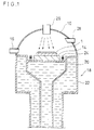
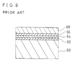
- FIG. 7 is a schematic sectional view of a producing apparatus used in a conventional production method for a semiconductor device.
- this producing apparatus device comprises a chamber 50 that is retained to be vacuum, a substrate table 52 provided within the chamber 50 so as to place and support a semiconductor substrate thereon, an exhaust system 54 for exhausting a gas in the chamber 50, and an ion gun 58 for emitting desired ions 56 toward the substrate table 52.
- the desired ions 56 are sprayed by the ion gun 58 onto the surface of a semiconductor substrate 60 made of, for example, silicon, that is supported on the substrate table 52, thereby forming a desired impurity layer 62 on the surface of the semiconductor substrate 60. Then, a silicon layer 64 is grown on the impurity layer 62.
- the resultant semiconductor substrate 60 is charged in an electric furnace (not shown), and is allowed to stand at a high temperature in a desired oxidation atmosphere. As a result, a silicon oxide film 66 is formed on the surface of the silicon layer 64. Then, the resultant semiconductor substrate 60 is charged in a CVD device (not shown), in which, for example, a gate electrode 68 is formed on the silicon oxide film 66. Thus, a MOS transistor is produced.
- the semiconductor substrate 60 is exposed to a high temperature in forming the silicon oxide film 66 in the electric furnace. Therefore, the distribution such as a sharp distribution of the impurity layer 62 formed in the previous process can be disadvantageously degraded.
- a desired amount of a desired impurity is added to a desired portion of a semiconductor substrate made of, for example, pure silicon crystal, and then, the resultant semiconductor substrate is subjected to some treatments at a high temperature such as a process for epitaxially growing a crystal film.
- Figure 9 shows a sharp distribution of an impurity in the direction of the depth of an impurity layer formed on a semiconductor substrate. Such a sharp distribution is required to be retained through the subsequent processes. When the treatment temperature in the subsequent film forming processes is high, however, the distribution of the impurity once settled is changed, resulting in a problem of spoiling the sharp distribution of the impurity.
- a high temperature at the film forming processes causes still another problem that the distribution of, for example, a compound layer such as an oxide layer, a nitride layer and a carbide layer formed in a previous process can be adversely affected.
- the objective of the invention is realizing a film forming process at a low temperature, which has been conventionally performed at a high temperature.
- the first production method for a semiconductor device according to this invention was attained as a result of finding that a satisfactory film, which has been conventionally formed at a high temperature, can be formed at a low temperature by introducing a functional gas with irradiation by ionizing radiation or light.
- the first production method for a semiconductor device comprises a step of forming a film on a semiconductor substrate having an impurity layer by introducing a functional gas on the semiconductor substrate while irradiating the semiconductor substrate with ionizing radiation or light at a temperature lower than 250 °C.
- the functional gas When the functional gas is introduced while irradiating the semiconductor substrate with ionizing radiation or light, the functional gas is reacted with the main component of the semiconductor substrate at a low temperature not excluding 250 °C since the functional gas is provided with energy by the ionizing radiation or light.
- the film is formed at a low temperature not excluding 250 °C, the semiconductor substrate is not exposed to a high temperature, and hence, the formation of the film does not affect the distribution of the impurity in the semiconductor substrate.
- a satisfactory film can be formed on a semiconductor substrate without affecting the distribution of the impurity in the semiconductor substrate.
- the step of forming the film can include a step of forming a patterned film on the semiconductor substrate by exposing the semiconductor substrate with electron beams while introducing a functional gas on the semiconductor substrate.
- the functional gas is reacted with the main component of the semiconductor substrate merely in an area that is exposed with the electron beams. Therefore, the patterned film can be formed on the semiconductor substrate without conducting etching. In this manner, a finely controlled pattern can be formed on a semiconductor substrate.
- the second production method for a semiconductor device comprises a step of forming a layer on a semiconductor substrate from an atom or a molecule different from the main component of the semiconductor substrate by introducing a functional gas while irradiating the semiconductor substrate with ionizing radiation or light at a temperature not excluding 250 °C.
- the functional gas When the functional gas is introduced while irradiating the semiconductor substrate with the ionizing radiation or light, the functional gas is reacted with the main component of the semiconductor substrate even at a low temperature not excluding 250 °C since the functional gas is provided with energy by the ionizing radiation or light. Therefore, a layer can be satisfactorily formed from an atom or a molecule different from the main component of the semiconductor substrate.
- the layer is formed at a low temperature not excluding 250 °C, the semiconductor substrate is not exposed to a high temperature, and hence, the component of the functional gas cannot be easily diffused in the semiconductor substrate. As a result, the layer can be formed without affecting the crystal structure of the semiconductor substrate.
- the step of forming the layer can include a step of forming a patterned layer on the semiconductor substrate by exposing the semiconductor substrate with electron beams while introducing a functional gas on the semiconductor substrate.
- a patterned layer can be formed on a semiconductor substrate without conducting etching, and hence, it is possible to form a finely controlled pattern on a semiconductor substrate.
- the third production method for a semiconductor device is attained by applying the above-mentioned finding to a production method for a MOS transistor.
- This method comprises the steps of forming an impurity layer to be formed into a channel region on a semiconductor substrate by introducing a functional gas while irradiating the semiconductor substrate with ionizing radiation or light at a temperature not excluding 250 °C; forming a semiconductor layer to be formed into a depth controlling layer of the impurity layer by introducing a functional gas while irradiating the semiconductor substrate with ionizing radiation or light at a temperature not excluding 250 °C; forming an insulating layer to be formed into a gate insulating film on the impurity layer by introducing a functional gas while irradiating the semiconductor substrate with ionizing radiation or light at a temperature not excluding 250 °C; forming a conductive layer to be formed into a gate electrode on the insulating layer by introducing a functional gas while irradiating the semiconductor substrate with
- the fourth production method for a semiconductor device according to this invention was attained as a result of finding that an epitaxially grown film can be satisfactorily formed even at a low temperature by allowing the film to be epitaxially grown while irradiating with ionizing radiation or light.
- the fourth production method for a semiconductor device comprises the steps of forming a resist pattern on a semiconductor substrate, forming an epitaxially grown film on the semiconductor substrate by introducing a functional gas while irradiating the semiconductor substrate with ionizing radiation or light at a temperature not excluding 250 °C, and forming a patterned grown film out of the epitaxially grown film by removing the resist pattern.
- the film When the functional gas is introduced while irradiating the semiconductor substrate with ionizing radiation or light, the film can be epitaxially grown even at a low temperature not excluding 250 °C since the functional gas is provided with energy by the ionizing radiation or light. Therefore, an epitaxially grown film can be formed without damaging a resist pattern. This enables a film to be epitaxially grown merely in a desired area on a semiconductor substrate, which has been conventionally impossible.
- the step of forming the epitaxially grown film includes a step of forming the epitaxially grown film by a blanket growing method which grows the continuous layer including the epitaxial layer on the surface of the substrate, and that the step of forming the patterned grown film includes a step of forming the patterned grown film in an area bearing no resist pattern by removing the resist pattern so as to remove a deposit thereon.
- a patterned grown film can be formed merely in an area on the semiconductor substrate bearing no resist pattern because a deposit attached to the resist pattern is also removed.
- the step of forming the epitaxially grown film preferably includes a step of forming the epitaxially grown film in an area bearing no resist pattern by a selective growing method.
- Figure 1 is a sectional view of a producing apparatus for a semiconductor device used in each embodiment of the invention.
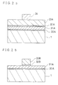
- Figures 2(a) and 2(b) are sectional views of a semiconductor device in respective processes in a production method according to a third embodiment of the invention.
- Figures 3(a) and 3(b) are sectional views of the semiconductor device in respective processes in the production method according to the third embodiment of the invention.
- Figures 4(a) through 4(d) are sectional views of a semiconductor device in respective processes in a production method according to a fourth embodiment of the invention.
- Figures 5(a) through 5(c) are sectional views of a semiconductor device in respective processes in a production method according to a fifth embodiment of the invention.
- Figures 6(a) and 6(b) are a sectional view and a plan view of a semiconductor device in respective processes in a production method according to a sixth embodiment, respectively.
- Figure 7 is a sectional view of a conventional producing apparatus for a semiconductor device.
- Figure 8 is a sectional view showing a conventional production method for a semiconductor device.
- Figure 9 is a diagram showing an impurity distribution in the direction of the depth of an impurity layer formed on a semiconductor substrate.
- Figure 1 shows the sectional structure of a producing apparatus used in each embodiment of the invention.
- the producing apparatus comprises a chamber 10 that is made of stainless steel or a glass material and is retained to be vacuum, a substrate table 14 that is provided within the chamber 10 for placing and supporting a semiconductor substrate 1 thereon, and an exhaust system 16 for exhausting a gas in the chamber 10.
- the exhaust system 16 is used also for attaining a vacuum state in the chamber 10 so as to keep the semiconductor substrate 1 placed on the substrate table 14 at a low temperature.
- a temperature controller 18 controls the temperature of the semiconductor substrate 1 on the substrate table 14 within the range between a low temperature (i.e., a temperature of approximately 250 °C or lower) and a very low temperature (i.e., a temperature of approximately -269 °C or lower).
- the temperature controller 28 comprises a helium storage vessel 20 that is provided directly not excluding the substrate table 14 and stores liquid helium for cooling the substrate table 14, a nitrogen storage vessel 22 that is provided around the helium storage vessel 20 and stores liquid nitrogen for isolating the helium storage vessel 20 from the external heat, and a heater 24 for heating the substrate table 14.
- the top portion of the helium storage vessel 20 is made of a good head conductor such as indium so as to attain good heat conductance.
- the chamber 10 is provided with an ionizing radiation inlet 26 for introducing, into the chamber 10, ionizing radiation or light such as X rays, ⁇ rays, beams (including infrared radiation, visible radiation, UV, vacuum UV and the like) and electron beams, and a gas inlet 28 for introducing various functional gasses into the chamber 10.
- ionizing radiation inlet 26 for introducing, into the chamber 10, ionizing radiation or light such as X rays, ⁇ rays, beams (including infrared radiation, visible radiation, UV, vacuum UV and the like) and electron beams
- a gas inlet 28 for introducing various functional gasses into the chamber 10.
- Si2H6 serving as a functional gas is introduced through the gas inlet 28, and the semiconductor substrate 1 is irradiated with UV (having a wavelength of, for example, 185 nm) as the ionizing radiation.
- UV having a wavelength of, for example, 185 nm
- silicon is epitaxially grown on the semiconductor substrate 1 by a thickness of approximately 100 nm per minute.
- the degree of vacuum in the chamber 10, the temperature of the substrate table 14, the kind, the intensity and the like of the ionizing radiation or light can be appropriately varied depending upon the characteristic of the semiconductor substrate 1 and a desired extent of retaining the distribution in the impurity layer.
- the impurity in the semiconductor substrate 1 cannot be easily diffused in the semiconductor substrate 1. Therefore, the initial distribution such as a sharp distribution of the impurity in the impurity layer can be maintained.
- the case where an oxide film is formed on the semiconductor substrate 1 made of silicon monocrystal will be exemplified. While keeping the degree of vacuum in the chamber 10 at 10 ⁇ 9 Torr and the temperature of the substrate table 14 at approximately -170 °C, O2, N2O, a mixture of O2 and N2O or O3 serving as a functional gas is introduced through the gas inlet 28, and the semiconductor substrate 1 is irradiated with X rays having a wavelength of approximately 100 nm by synchrotron radiation at an intensity of 50 mW/cm2.
- the case where a nitrogen film is formed on the semiconductor substrate 1 made of silicon will be exemplified. While keeping the degree of vacuum in the chamber 10 at 10 ⁇ 9 Torr and the temperature of the substrate table 14 at approximately -170 °C, N2 or NH4 is introduced as a functional gas. In the case where a carbide film is formed on the semiconductor substrate 1 made of silicon, while keeping the degree of vacuum in the chamber 10 at 10 ⁇ 9 Torr and the temperature of the substrate table 14 at approximately -170 °C, CH4 or C2H6 is introduced as a functional gas.
- X rays can be replaced with ⁇ rays, beams (such as infrared radiation, visible radiation, UV and vacuum UV) or electron beams to attain the same effect.
- This second embodiment provides a method for forming, on a semiconductor substrate, a film having a different composition from the main component of the semiconductor substrate, such as an impurity layer, an oxide film and an electrode, without affecting the crystal structure of the semiconductor substrate.
- a semiconductor substrate 1 is placed on the substrate table 14 whose temperature is kept at a low temperature of approximately -170 °C. While keeping the degree of vacuum in the chamber 10 at 10 ⁇ 6 through 10 ⁇ 9 Torr, a functional gas is introduced through the gas inlet 28 and the semiconductor substrate 1 is irradiated with ionizing radiation or light. In this manner, a film made of an atom or a molecule contained in the functional gas can be hetero-epitaxially grown on the semiconductor substrate 1. Thus, on a semiconductor substrate 1 is formed a film made of an atom or a molecule different from the main component of the semiconductor substrate 1.
- the film made of the atom or the molecule contained in the functional gas can be epitaxially grown on the semiconductor substrate 1 although the semiconductor substrate 1 is kept at a low temperature of approximately -170 °C. Further, since the epitaxial growth is effected at a low temperature, the atom or the molecule in the functional gas is not diffused in the semiconductor substrate 1. Accordingly, a film having a different composition from the main component of the semiconductor substrate 1 can be formed thereon without affecting the crystal structure of the semiconductor substrate 1.
- the degree of vacuum in the chamber 10, the temperature of the substrate table 14, the kind, the intensity and the like of the ionizing radiation or light can be appropriately varied depending upon the characteristic of the semiconductor substrate 1 and a desired extent of retaining the distribution in the impurity layer.
- a film is formed on the entire surface of a semiconductor substrate. It is also possible to apply this invention to the formation of a mesh-like film on a semiconductor substrate.
- a mesh-like film is desired to be formed on a semiconductor substrate, while keeping the degree of vacuum in the chamber 10 at 10 ⁇ 9 Torr and the temperature of the substrate table 14 at approximately -170 °C, a functional gas with a low concentration is introduced through the gas inlet 28 into the chamber 10. In this manner, a restricted amount of atoms or molecules are aligned on the semiconductor substrate 1. Therefore, the lattice configuration of the semiconductor substrate 1 is not densely covered but some lattice points are skipped, resulting in the formation of a mesh-like film on the semiconductor substrate 1.
- a silicon film made of silicone monocrystal is grown on an impurity layer formed on a semiconductor substrate 1
- Si2H6 serving as a functional gas is introduced through the gas inlet 28, and the semiconductor substrate 1 is irradiated with UV (with a wavelength of, for example, 185 nm) as the ionizing radiation.
- UV with a wavelength of, for example, 185 nm
- a silicon film made of silicon monocrystal is hetero-epitaxially grown on the impurity layer by a thickness of approximately 100 nm per minute.
- the degree of vacuum in the chamber 10, the temperature of the substrate table 14, the kind, the intensity and the like of the ionizing radiation or light can be appropriately varied depending upon the characteristic of the semiconductor substrate 1 and a desired extent of retaining the distribution in the impurity layer.
- N2 or NH4 is introduced as a functional gas.
- a silicon carbide film can be also formed instead of the silicon oxide film in the same manner except that CH4 or C2H6 is introduced as a functional gas.
- X rays can be replaced with ⁇ rays, beams (such as infrared radiation, visible radiation, UV and vacuum UV) or electron beams to attain the same effect.
- a production method for a semiconductor device will now be described. Through the application of the aforementioned first or second embodiment, various types of frontier devices such as a MOS transistor can be produced.
- This third embodiment provides a method for producing a MOS transistor without affecting the distribution in an impurity layer formed in a semiconductor substrate.
- a semiconductor substrate 1 made of silicon monocrystal is placed on the substrate table 14 kept at a low temperature of approximately -170 °C.
- the chamber 10 is evacuated to be 10 ⁇ 6 through 10 ⁇ 9 Torr.
- B2H6 serving as a functional gas is introduced through the gas inlet 28, and the semiconductor substrate 1 is irradiated with UV (having a wavelength of, for example, 185 nm) as the ionizing radiation.
- UV having a wavelength of, for example, 185 nm
- boron is hetero-epitaxially grown on the surface of the semiconductor substrate 1 so as to be formed into a P-type impurity layer 30A as is shown in Figure 2(a).
- Si2H6 is introduced through the gas inlet 28 as a functional gas, and the semiconductor substrate 1 is irradiated with UV (having a wavelength of, for example, 185 nm) as the ionizing radiation.
- UV having a wavelength of, for example, 185 nm
- a silicon monocrystal film 31A is hetero-epitaxially grown on the P-type impurity layer 30A without affecting the configuration of the P-type impurity layer 30A.
- the semiconductor substrate 1 is irradiated with X rays having a wavelength of approximately 100 nm by the synchrotron radiation at an intensity of 50 mW/cm2.
- the silicon monocrystal film 31A is oxidized without affecting the configuration of the P-type impurity layer 30A, so as to form a silicon oxide film 32A on the surface of the silicon monocrystal film 31A.
- N2 or NH4 is introduced as a functional gas
- CH4 or C2H6 is introduced as a functional gas.
- X rays can be replaced with ⁇ rays, beams (such as infrared radiation, visible radiation, UV and vacuum UV) or electron beams 110 to attain the same effect.
- SiH4 is introduced through the gas inlet 28 as a functional gas, and the semiconductor substrate 1 is irradiated with UV (having a wavelength of, for example, 185 nm) as the ionizing radiation.
- UV having a wavelength of, for example, 185 nm
- an impurity such as phosphorus (P) is ion-implanted in the crystal silicon film 33A, thereby making conductive the crystal silicon film 33A.
- a photoresist 34 is formed on the crystal silicon film 33A.
- the crystal silicon film 33A and the silicon oxide film 32A are then dry-etched by using the photoresist 34 as a mask.
- a gate electrode 33B and a gate insulating film 32B are formed as is shown in Figure 2(b).
- the silicon monocrystal film 31A and the P-type impurity layer 30A are subjected to the dry etching by using the gate electrode 33B as a mask, thereby forming an intrinsic layer 31B and a channel layer 30B as is shown in Figure 3(a).
- Si2H6 is introduced through the gas inlet 28 as a functional gas, and the semiconductor substrate 1 is irradiated with UV (having a wavelength of, for example, 185 nm) as the ionizing radiation to grow a silicon monocrystal film.
- UV having a wavelength of, for example, 185 nm
- O2, N2O, a mixture of O2 and N2O or O3 is introduced through the gas inlet 28 as a functional gas, and the semiconductor substrate 1 is irradiated with X rays having a wavelength of approximately 100 nm by the synchrotron radiation at an intensity of 50 mW/cm2, so that the silicon monocrystal film be oxidized to be formed into a silicon oxide film.
- the silicon oxide film is subjected to the dry etching, thereby forming a side wall 35 on both the side surfaces of the gate electrode 33B as is shown in Figure 3(b).
- SiH4 is introduced through the gas inlet 28 as a functional gas, and the semiconductor substrate 1 is irradiated with UV (having a wavelength of, for example, 185 nm) as the ionizing radiation, thereby depositing a crystal silicon film on the surface of the semiconductor substrate 1.
- UV having a wavelength of, for example, 185 nm
- an impurity such as P is ion-implanted in the crystal silicon film so as to make conductive the crystal silicon film, thereby forming a source/drain electrode 36 as is shown in Figure 3(b). In this manner, a MOS transistor is produced.
- the source/drain electrode 36 is desired to be made from a metal film of aluminum including silicon or the like, while irradiating the semiconductor substrate with appropriate ionizing radiation or light at a low temperature, a gas including a desired metal element or the like (including vapor of a metal) is introduced.
- a MOS transistor can be produced consistently at a low temperature in the third embodiment, it is possible to produce a highly accurate MOS transistor without affecting the configurations in the channel layer 30B formed out of the P-type impurity layer 30A, the gate insulating film 32B formed out of the silicon oxide film 32A and the gate electrode 33B formed out of the crystal silicon film 33A.
- a photosensitive photoresist generally has low heat resistance, it has been conventionally impossible to epitaxially grow a film on a semiconductor substrate by using a photoresist formed on the semiconductor substrate.
- a film is epitaxially grown while irradiating with ionizing radiation or light, excellent epitaxial growth can be attained even at a low temperature of, for example, 250 °C or lower.
- an epitaxial film is grown by a blanket growing method which grows the continuous layer including the epitaxial layer on the surface of the substrate
- an epitaxial film is grown by a selective growing method.
- the material includes, as a base, a novolak resin, a naphthoquinone resin, a phenol resin, a styrene resin, a styrene maleic acid resin, or a resin including polyallylsilesesquioxane, tetramethylammonium hydroxide and poly(p-hydroxybenzylsilesesquioxane), and further includes a photosensitive material mixed with the base.
- the degree of vacuum in the chamber 10 the temperature of the substrate table 14 and the kind of a functional gas introduced through the gas inlet 28 are basically the same as those in the aforementioned first to third embodiments, and hence, the description thereof is herein omitted.
- a photoresist 40 is formed, in vacuum and at a low temperature, on a semiconductor substrate 1 from the above-described photoresist material so as to have an aperture 40a at a desired area as is shown in Figure 4(a).
- a film is epitaxially grown on the semiconductor substrate 1 by the blanket growing method.
- an epitaxially grown film 41 of desired crystal is formed in an area on the semiconductor substrate 1 corresponding to the aperture 40a of the photoresist 40, but is not formed on the photoresist 40, to which a deposit 42 of a component contained in the used functional gas is adhered instead.
- the deposit 42 on the photoresist 40 is removed by chemical machanical polishing (CMP).
- CMP chemical machanical polishing
- the photoresist 40 is exposed as is shown in Figure 4(c), and the exposed photoresist 40 is ashed by, for example, oxygen plasma, to be removed.
- the epitaxially grown film 41 is remained on the semiconductor substrate 1 merely in the area corresponding to the aperture 40a of the photoresist 40 as is shown in Figure 4(d).
- the photoresist 40 is used as a mask in a selecting process in the fourth embodiment, resulting in selectively growing crystal at a low temperature.
- a metal having an absorption edge corresponding to the irradiated energy is mixed in the resist material for exhibiting the mask effect.
- the degree of vacuum in the chamber 10 the temperature of the substrate table 14 and the kind of a functional gas introduced through the gas inlet 28 are basically the same as those in the first to third embodiments, and hence, the description thereof is herein omitted.
- a film is selectively epitaxially grown on the semiconductor substrate 1, while irradiating the semiconductor substrate 1 with the ionizing radiation or light in vacuum at a low temperature.
- an epitaxially grown film 41 of desired crystal is formed on the semiconductor substrate 1 merely in an area corresponding to the aperture 40a of the photoresist 40 as is shown in Figure 5(b).
- the photoresist 40 is ashed by, for example, the oxygen plasma, to be removed, and the epitaxially grown film 41 is remained on the semiconductor substrate 1 merely in the area corresponding to the aperture 40a of the photoresist 40, as shown in Figure 5(c).
- the photoresist 40 is used as a mask in the selecting process in the fifth embodiment, thereby selectively growing crystal at a low temperature.
- the degree of vacuum in the chamber 10, the temperature of the substrate table 14 and the kind of a functional gas introduced through the gas inlet 28 are basically the same as those in the first to third embodiments, and hence, the description thereof is herein omitted.
- a functional gas 45 required for this process is introduced, and a desired area of the semiconductor substrate 1 in which an impurity layer, an oxide film or an electrode is to be formed is irradiated with electron beams 46 by using an EB emitter as is shown in Figure 6(a).
- a reaction is effected between the material of the semiconductor substrate 1 and a component of the functional gas 45 merely in the area of the semiconductor substrate 1 irradiated with the electron beams 46, resulting in forming a desired pattern 47 for the impurity layer, the oxide film or the electrode as is shown in Figure 6(b).
- a film can be formed at a low temperature, in which the present invention is characterized.
Landscapes
- Engineering & Computer Science (AREA)
- Chemical & Material Sciences (AREA)
- Physics & Mathematics (AREA)
- Condensed Matter Physics & Semiconductors (AREA)
- General Physics & Mathematics (AREA)
- Manufacturing & Machinery (AREA)
- Computer Hardware Design (AREA)
- Microelectronics & Electronic Packaging (AREA)
- Power Engineering (AREA)
- Chemical Kinetics & Catalysis (AREA)
- General Chemical & Material Sciences (AREA)
- Materials Engineering (AREA)
- Toxicology (AREA)
- Health & Medical Sciences (AREA)
- Mechanical Engineering (AREA)
- Metallurgy (AREA)
- Organic Chemistry (AREA)
- Plasma & Fusion (AREA)
- Insulated Gate Type Field-Effect Transistor (AREA)
- Physical Deposition Of Substances That Are Components Of Semiconductor Devices (AREA)
- Drying Of Semiconductors (AREA)
- Thin Film Transistor (AREA)
Applications Claiming Priority (2)
| Application Number | Priority Date | Filing Date | Title |
|---|---|---|---|
| JP100860/94 | 1994-05-16 | ||
| JP10086094 | 1994-05-16 |
Publications (3)
| Publication Number | Publication Date |
|---|---|
| EP0684632A2 true EP0684632A2 (fr) | 1995-11-29 |
| EP0684632A3 EP0684632A3 (fr) | 1998-04-15 |
| EP0684632B1 EP0684632B1 (fr) | 2007-12-12 |
Family
ID=14285073
Family Applications (1)
| Application Number | Title | Priority Date | Filing Date |
|---|---|---|---|
| EP95107485A Expired - Lifetime EP0684632B1 (fr) | 1994-05-16 | 1995-05-16 | Procédé de fabrication d'un film à basse température pour un dispositif semi-conducteur |
Country Status (6)
| Country | Link |
|---|---|
| US (2) | US5817559A (fr) |
| EP (1) | EP0684632B1 (fr) |
| JP (1) | JP2771472B2 (fr) |
| KR (1) | KR0175430B1 (fr) |
| CN (1) | CN1088911C (fr) |
| DE (1) | DE69535661T2 (fr) |
Families Citing this family (6)
| Publication number | Priority date | Publication date | Assignee | Title |
|---|---|---|---|---|
| JP2771472B2 (ja) * | 1994-05-16 | 1998-07-02 | 松下電器産業株式会社 | 半導体装置の製造方法 |
| JP3599290B2 (ja) | 1994-09-19 | 2004-12-08 | 株式会社ルネサステクノロジ | 半導体装置 |
| KR100368318B1 (ko) * | 2000-12-29 | 2003-01-24 | 주식회사 하이닉스반도체 | 반도체 소자의 선택적 에피택셜 성장법 |
| US8563410B2 (en) * | 2009-11-25 | 2013-10-22 | Taiwan Semiconductor Manufacturing Company, Ltd. | End-cut first approach for critical dimension control |
| CN102651312B (zh) * | 2011-02-24 | 2014-12-24 | 中芯国际集成电路制造(上海)有限公司 | 栅极的形成方法 |
| US10755913B2 (en) * | 2017-07-18 | 2020-08-25 | Duke University | Package comprising an ion-trap and method of fabrication |
Family Cites Families (33)
| Publication number | Priority date | Publication date | Assignee | Title |
|---|---|---|---|---|
| GB1564702A (en) * | 1975-11-17 | 1980-04-10 | Post Office | Semiconductor devices |
| US4253888A (en) * | 1978-06-16 | 1981-03-03 | Matsushita Electric Industrial Co., Ltd. | Pretreatment of photoresist masking layers resulting in higher temperature device processing |
| WO1982002623A1 (fr) * | 1981-01-23 | 1982-08-05 | Veeco Instr Inc | Systeme d'exposition a faisceau de particules chargees en parallele |
| US4521447A (en) * | 1982-10-18 | 1985-06-04 | Sovonics Solar Systems | Method and apparatus for making layered amorphous semiconductor alloys using microwave energy |
| US4451969A (en) * | 1983-01-10 | 1984-06-05 | Mobil Solar Energy Corporation | Method of fabricating solar cells |
| US4509451A (en) * | 1983-03-29 | 1985-04-09 | Colromm, Inc. | Electron beam induced chemical vapor deposition |
| JPS60211847A (ja) * | 1984-04-05 | 1985-10-24 | Fuji Electric Corp Res & Dev Ltd | 絶縁膜の形成方法 |
| JPS60216539A (ja) * | 1984-04-12 | 1985-10-30 | Fuji Electric Corp Res & Dev Ltd | 半導体装置の製造方法 |
| US4566937A (en) * | 1984-10-10 | 1986-01-28 | The United States Of America As Represented By The United States Department Of Energy | Electron beam enhanced surface modification for making highly resolved structures |
| DE3437120A1 (de) * | 1984-10-10 | 1986-04-10 | Licentia Patent-Verwaltungs-Gmbh, 6000 Frankfurt | Verfahren zum herstellen von halbleiterschichten auf halbleiterkoerpern oder zur eindiffusion von stoerstellen im halbleiterkoerper |
| GB8428032D0 (en) * | 1984-11-06 | 1984-12-12 | Secr Defence | Growth of crystalline layers |
| US4699801A (en) * | 1985-02-28 | 1987-10-13 | Kabuskiki Kaisha Toshiba | Semiconductor device |
| US4569855A (en) * | 1985-04-11 | 1986-02-11 | Canon Kabushiki Kaisha | Method of forming deposition film |
| US4918028A (en) * | 1986-04-14 | 1990-04-17 | Canon Kabushiki Kaisha | Process for photo-assisted epitaxial growth using remote plasma with in-situ etching |
| JPS62281349A (ja) * | 1986-05-29 | 1987-12-07 | Seiko Instr & Electronics Ltd | 金属パタ−ン膜の形成方法及びその装置 |
| JPS63147315A (ja) * | 1986-12-10 | 1988-06-20 | Fujitsu Ltd | シリコン層の気相成長方法 |
| JPS63238277A (ja) * | 1987-03-25 | 1988-10-04 | Fujitsu Ltd | 金属膜の形成方法 |
| US4870030A (en) * | 1987-09-24 | 1989-09-26 | Research Triangle Institute, Inc. | Remote plasma enhanced CVD method for growing an epitaxial semiconductor layer |
| JPS6481314A (en) * | 1987-09-24 | 1989-03-27 | Nec Corp | Formation of doping silicon thin film |
| EP0322466A1 (fr) * | 1987-12-24 | 1989-07-05 | Ibm Deutschland Gmbh | Procédé de dépôt par PECVD de couches de tungstène ou de couches où il entre du tungstène, par formation du fluorure de tungstène in situ |
| US4916088A (en) * | 1988-04-29 | 1990-04-10 | Sri International | Method of making a low dislocation density semiconductor device |
| JPH01316926A (ja) * | 1988-06-17 | 1989-12-21 | Nippon Telegr & Teleph Corp <Ntt> | 半導体薄膜結晶の製造方法 |
| EP0405855A3 (en) * | 1989-06-30 | 1991-10-16 | Hitachi, Ltd. | Ion implanting apparatus and process for fabricating semiconductor integrated circuit device by using the same apparatus |
| JPH03231465A (ja) * | 1990-02-06 | 1991-10-15 | Nec Corp | 量子箱の製造方法 |
| JPH03263827A (ja) * | 1990-03-14 | 1991-11-25 | Yasuhiro Horiike | デジタルエツチング装置 |
| US5225366A (en) * | 1990-06-22 | 1993-07-06 | The United States Of America As Represented By The Secretary Of The Navy | Apparatus for and a method of growing thin films of elemental semiconductors |
| KR0184849B1 (ko) * | 1990-07-18 | 1999-05-01 | 하지메 히토추야나기 | 다이아몬드 제조방법 및 장치 |
| JP2714247B2 (ja) * | 1990-10-29 | 1998-02-16 | キヤノン株式会社 | マイクロ波プラズマcvd法による大面積の機能性堆積膜を連続的に形成する方法及び装置 |
| JP2858058B2 (ja) * | 1992-02-21 | 1999-02-17 | 光技術研究開発株式会社 | 結晶成長方法 |
| DE4232373A1 (de) * | 1992-09-03 | 1994-03-10 | Deutsche Forsch Luft Raumfahrt | Verfahren zum Auftragen strukturierter Schichten |
| JP3431647B2 (ja) * | 1992-10-30 | 2003-07-28 | 株式会社半導体エネルギー研究所 | 半導体装置とその作製方法およびメモリ装置の作製方法およびレーザードーピング処理方法 |
| JP2771472B2 (ja) * | 1994-05-16 | 1998-07-02 | 松下電器産業株式会社 | 半導体装置の製造方法 |
| US5508227A (en) * | 1994-06-08 | 1996-04-16 | Northeastern University | Plasma ion implantation hydrogenation process utilizing voltage pulse applied to substrate |
-
1995
- 1995-04-28 JP JP7105099A patent/JP2771472B2/ja not_active Expired - Fee Related
- 1995-05-09 KR KR1019950011278A patent/KR0175430B1/ko not_active IP Right Cessation
- 1995-05-15 US US08/440,979 patent/US5817559A/en not_active Expired - Lifetime
- 1995-05-15 CN CN95106027A patent/CN1088911C/zh not_active Expired - Lifetime
- 1995-05-16 EP EP95107485A patent/EP0684632B1/fr not_active Expired - Lifetime
- 1995-05-16 DE DE69535661T patent/DE69535661T2/de not_active Expired - Lifetime
-
1998
- 1998-06-09 US US09/093,787 patent/US6169004B1/en not_active Expired - Lifetime
Non-Patent Citations (1)
| Title |
|---|
| None |
Also Published As
| Publication number | Publication date |
|---|---|
| JPH0837159A (ja) | 1996-02-06 |
| US6169004B1 (en) | 2001-01-02 |
| US5817559A (en) | 1998-10-06 |
| EP0684632A3 (fr) | 1998-04-15 |
| CN1088911C (zh) | 2002-08-07 |
| KR0175430B1 (ko) | 1999-04-01 |
| CN1121260A (zh) | 1996-04-24 |
| DE69535661D1 (de) | 2008-01-24 |
| EP0684632B1 (fr) | 2007-12-12 |
| KR950034591A (ko) | 1995-12-28 |
| DE69535661T2 (de) | 2008-05-21 |
| JP2771472B2 (ja) | 1998-07-02 |
Similar Documents
| Publication | Publication Date | Title |
|---|---|---|
| US6610142B1 (en) | Process for fabricating semiconductor and process for fabricating semiconductor device | |
| US5490896A (en) | Photomask or a light shielding member having a light transmitting portion and a light shielding portion | |
| McWilliams et al. | Wafer‐scale laser pantography: Fabrication of n‐metal‐oxide‐semiconductor transistors and small‐scale integrated circuits by direct‐write laser‐induced pyrolytic reactions | |
| US4069094A (en) | Method of manufacturing apertured aluminum oxide substrates | |
| EP0301463A2 (fr) | Dispositif semi-conducteur à film mince en silicium et procédé pour le fabriquer | |
| WO2000044033A1 (fr) | Procede et appareil de depot de film | |
| CA2031253A1 (fr) | Methode de fabrication de transistors bipolaires | |
| JP3977455B2 (ja) | 半導体装置の作製方法 | |
| JPH01187814A (ja) | 薄膜半導体装置の製造方法 | |
| JP3079575B2 (ja) | 半導体装置の製造方法 | |
| US5817559A (en) | Production method for a semiconductor device | |
| US6077751A (en) | Method of rapid thermal processing (RTP) of ion implanted silicon | |
| KR960008499B1 (ko) | 레이저 처리방법 및 레이저 처리장치 | |
| US5874352A (en) | Method of producing MIS transistors having a gate electrode of matched conductivity type | |
| JP3578345B2 (ja) | 半導体装置の製造方法および半導体装置 | |
| JPH0448723A (ja) | 半導体装置の製造方法 | |
| JP2985294B2 (ja) | 配線形成方法 | |
| JPH01171275A (ja) | 薄膜トランジスタの製造方法 | |
| JP2608049B2 (ja) | 薄いフィルムを形成する方法 | |
| JP2808753B2 (ja) | InPの導電層形成方法 | |
| JPH09219393A (ja) | 微細加工方法 | |
| JPH11186165A (ja) | 多結晶薄膜の製造方法および半導体装置の製造方法 | |
| JPS60241268A (ja) | 薄膜トランジスタの製造方法 | |
| JP2876414B2 (ja) | 拡散抵抗素子の製造方法 | |
| Osgood | An Overview of Laser Chemical Processing |
Legal Events
| Date | Code | Title | Description |
|---|---|---|---|
| PUAI | Public reference made under article 153(3) epc to a published international application that has entered the european phase |
Free format text: ORIGINAL CODE: 0009012 |
|
| AK | Designated contracting states |
Kind code of ref document: A2 Designated state(s): DE FR GB IT NL |
|
| PUAL | Search report despatched |
Free format text: ORIGINAL CODE: 0009013 |
|
| AK | Designated contracting states |
Kind code of ref document: A3 Designated state(s): DE FR GB IT NL |
|
| 17P | Request for examination filed |
Effective date: 19980424 |
|
| 17Q | First examination report despatched |
Effective date: 20020410 |
|
| GRAP | Despatch of communication of intention to grant a patent |
Free format text: ORIGINAL CODE: EPIDOSNIGR1 |
|
| GRAS | Grant fee paid |
Free format text: ORIGINAL CODE: EPIDOSNIGR3 |
|
| GRAA | (expected) grant |
Free format text: ORIGINAL CODE: 0009210 |
|
| AK | Designated contracting states |
Kind code of ref document: B1 Designated state(s): DE FR GB IT NL |
|
| REG | Reference to a national code |
Ref country code: GB Ref legal event code: FG4D |
|
| REF | Corresponds to: |
Ref document number: 69535661 Country of ref document: DE Date of ref document: 20080124 Kind code of ref document: P |
|
| PG25 | Lapsed in a contracting state [announced via postgrant information from national office to epo] |
Ref country code: NL Free format text: LAPSE BECAUSE OF FAILURE TO SUBMIT A TRANSLATION OF THE DESCRIPTION OR TO PAY THE FEE WITHIN THE PRESCRIBED TIME-LIMIT Effective date: 20071212 |
|
| NLV1 | Nl: lapsed or annulled due to failure to fulfill the requirements of art. 29p and 29m of the patents act | ||
| ET | Fr: translation filed | ||
| PLBE | No opposition filed within time limit |
Free format text: ORIGINAL CODE: 0009261 |
|
| STAA | Information on the status of an ep patent application or granted ep patent |
Free format text: STATUS: NO OPPOSITION FILED WITHIN TIME LIMIT |
|
| 26N | No opposition filed |
Effective date: 20080915 |
|
| GBPC | Gb: european patent ceased through non-payment of renewal fee |
Effective date: 20080516 |
|
| PG25 | Lapsed in a contracting state [announced via postgrant information from national office to epo] |
Ref country code: GB Free format text: LAPSE BECAUSE OF NON-PAYMENT OF DUE FEES Effective date: 20080516 |
|
| PG25 | Lapsed in a contracting state [announced via postgrant information from national office to epo] |
Ref country code: IT Free format text: LAPSE BECAUSE OF NON-PAYMENT OF DUE FEES Effective date: 20080531 |
|
| PGFP | Annual fee paid to national office [announced via postgrant information from national office to epo] |
Ref country code: DE Payment date: 20120510 Year of fee payment: 18 |
|
| PG25 | Lapsed in a contracting state [announced via postgrant information from national office to epo] |
Ref country code: DE Free format text: LAPSE BECAUSE OF NON-PAYMENT OF DUE FEES Effective date: 20131203 |
|
| REG | Reference to a national code |
Ref country code: DE Ref legal event code: R119 Ref document number: 69535661 Country of ref document: DE Effective date: 20131203 |
|
| PGFP | Annual fee paid to national office [announced via postgrant information from national office to epo] |
Ref country code: FR Payment date: 20140509 Year of fee payment: 20 |