EP0540247A2 - Fabrication de modules multi-puce - Google Patents
Fabrication de modules multi-puce Download PDFInfo
- Publication number
- EP0540247A2 EP0540247A2 EP92309667A EP92309667A EP0540247A2 EP 0540247 A2 EP0540247 A2 EP 0540247A2 EP 92309667 A EP92309667 A EP 92309667A EP 92309667 A EP92309667 A EP 92309667A EP 0540247 A2 EP0540247 A2 EP 0540247A2
- Authority
- EP
- European Patent Office
- Prior art keywords
- carrier
- circuitized
- dielectric
- layer
- flexible carrier
- Prior art date
- Legal status (The legal status is an assumption and is not a legal conclusion. Google has not performed a legal analysis and makes no representation as to the accuracy of the status listed.)
- Withdrawn
Links
Images


Classifications
-
- H—ELECTRICITY
- H05—ELECTRIC TECHNIQUES NOT OTHERWISE PROVIDED FOR
- H05K—PRINTED CIRCUITS; CASINGS OR CONSTRUCTIONAL DETAILS OF ELECTRIC APPARATUS; MANUFACTURE OF ASSEMBLAGES OF ELECTRICAL COMPONENTS
- H05K3/00—Apparatus or processes for manufacturing printed circuits
- H05K3/46—Manufacturing multilayer circuits
- H05K3/4688—Composite multilayer circuits, i.e. comprising insulating layers having different properties
- H05K3/4691—Rigid-flexible multilayer circuits comprising rigid and flexible layers, e.g. having in the bending regions only flexible layers
-
- H—ELECTRICITY
- H01—ELECTRIC ELEMENTS
- H01L—SEMICONDUCTOR DEVICES NOT COVERED BY CLASS H10
- H01L23/00—Details of semiconductor or other solid state devices
- H01L23/52—Arrangements for conducting electric current within the device in operation from one component to another, i.e. interconnections, e.g. wires, lead frames
- H01L23/538—Arrangements for conducting electric current within the device in operation from one component to another, i.e. interconnections, e.g. wires, lead frames the interconnection structure between a plurality of semiconductor chips being formed on, or in, insulating substrates
- H01L23/5385—Assembly of a plurality of insulating substrates
-
- H—ELECTRICITY
- H01—ELECTRIC ELEMENTS
- H01L—SEMICONDUCTOR DEVICES NOT COVERED BY CLASS H10
- H01L23/00—Details of semiconductor or other solid state devices
- H01L23/52—Arrangements for conducting electric current within the device in operation from one component to another, i.e. interconnections, e.g. wires, lead frames
- H01L23/538—Arrangements for conducting electric current within the device in operation from one component to another, i.e. interconnections, e.g. wires, lead frames the interconnection structure between a plurality of semiconductor chips being formed on, or in, insulating substrates
- H01L23/5387—Flexible insulating substrates
-
- H—ELECTRICITY
- H01—ELECTRIC ELEMENTS
- H01L—SEMICONDUCTOR DEVICES NOT COVERED BY CLASS H10
- H01L25/00—Assemblies consisting of a plurality of individual semiconductor or other solid state devices ; Multistep manufacturing processes thereof
- H01L25/16—Assemblies consisting of a plurality of individual semiconductor or other solid state devices ; Multistep manufacturing processes thereof the devices being of types provided for in two or more different main groups of groups H01L27/00 - H01L33/00, or in a single subclass of H10K, H10N, e.g. forming hybrid circuits
-
- H—ELECTRICITY
- H05—ELECTRIC TECHNIQUES NOT OTHERWISE PROVIDED FOR
- H05K—PRINTED CIRCUITS; CASINGS OR CONSTRUCTIONAL DETAILS OF ELECTRIC APPARATUS; MANUFACTURE OF ASSEMBLAGES OF ELECTRICAL COMPONENTS
- H05K1/00—Printed circuits
- H05K1/18—Printed circuits structurally associated with non-printed electric components
- H05K1/189—Printed circuits structurally associated with non-printed electric components characterised by the use of a flexible or folded printed circuit
-
- H—ELECTRICITY
- H01—ELECTRIC ELEMENTS
- H01L—SEMICONDUCTOR DEVICES NOT COVERED BY CLASS H10
- H01L2224/00—Indexing scheme for arrangements for connecting or disconnecting semiconductor or solid-state bodies and methods related thereto as covered by H01L24/00
- H01L2224/01—Means for bonding being attached to, or being formed on, the surface to be connected, e.g. chip-to-package, die-attach, "first-level" interconnects; Manufacturing methods related thereto
- H01L2224/10—Bump connectors; Manufacturing methods related thereto
- H01L2224/15—Structure, shape, material or disposition of the bump connectors after the connecting process
- H01L2224/16—Structure, shape, material or disposition of the bump connectors after the connecting process of an individual bump connector
- H01L2224/161—Disposition
- H01L2224/16151—Disposition the bump connector connecting between a semiconductor or solid-state body and an item not being a semiconductor or solid-state body, e.g. chip-to-substrate, chip-to-passive
- H01L2224/16221—Disposition the bump connector connecting between a semiconductor or solid-state body and an item not being a semiconductor or solid-state body, e.g. chip-to-substrate, chip-to-passive the body and the item being stacked
- H01L2224/16225—Disposition the bump connector connecting between a semiconductor or solid-state body and an item not being a semiconductor or solid-state body, e.g. chip-to-substrate, chip-to-passive the body and the item being stacked the item being non-metallic, e.g. insulating substrate with or without metallisation
-
- H—ELECTRICITY
- H01—ELECTRIC ELEMENTS
- H01L—SEMICONDUCTOR DEVICES NOT COVERED BY CLASS H10
- H01L2224/00—Indexing scheme for arrangements for connecting or disconnecting semiconductor or solid-state bodies and methods related thereto as covered by H01L24/00
- H01L2224/01—Means for bonding being attached to, or being formed on, the surface to be connected, e.g. chip-to-package, die-attach, "first-level" interconnects; Manufacturing methods related thereto
- H01L2224/26—Layer connectors, e.g. plate connectors, solder or adhesive layers; Manufacturing methods related thereto
- H01L2224/31—Structure, shape, material or disposition of the layer connectors after the connecting process
- H01L2224/32—Structure, shape, material or disposition of the layer connectors after the connecting process of an individual layer connector
- H01L2224/321—Disposition
- H01L2224/32151—Disposition the layer connector connecting between a semiconductor or solid-state body and an item not being a semiconductor or solid-state body, e.g. chip-to-substrate, chip-to-passive
- H01L2224/32221—Disposition the layer connector connecting between a semiconductor or solid-state body and an item not being a semiconductor or solid-state body, e.g. chip-to-substrate, chip-to-passive the body and the item being stacked
- H01L2224/32225—Disposition the layer connector connecting between a semiconductor or solid-state body and an item not being a semiconductor or solid-state body, e.g. chip-to-substrate, chip-to-passive the body and the item being stacked the item being non-metallic, e.g. insulating substrate with or without metallisation
-
- H—ELECTRICITY
- H01—ELECTRIC ELEMENTS
- H01L—SEMICONDUCTOR DEVICES NOT COVERED BY CLASS H10
- H01L2224/00—Indexing scheme for arrangements for connecting or disconnecting semiconductor or solid-state bodies and methods related thereto as covered by H01L24/00
- H01L2224/73—Means for bonding being of different types provided for in two or more of groups H01L2224/10, H01L2224/18, H01L2224/26, H01L2224/34, H01L2224/42, H01L2224/50, H01L2224/63, H01L2224/71
- H01L2224/732—Location after the connecting process
- H01L2224/73201—Location after the connecting process on the same surface
- H01L2224/73203—Bump and layer connectors
- H01L2224/73204—Bump and layer connectors the bump connector being embedded into the layer connector
-
- H—ELECTRICITY
- H01—ELECTRIC ELEMENTS
- H01L—SEMICONDUCTOR DEVICES NOT COVERED BY CLASS H10
- H01L2924/00—Indexing scheme for arrangements or methods for connecting or disconnecting semiconductor or solid-state bodies as covered by H01L24/00
- H01L2924/15—Details of package parts other than the semiconductor or other solid state devices to be connected
- H01L2924/151—Die mounting substrate
- H01L2924/1517—Multilayer substrate
- H01L2924/15192—Resurf arrangement of the internal vias
-
- H—ELECTRICITY
- H01—ELECTRIC ELEMENTS
- H01L—SEMICONDUCTOR DEVICES NOT COVERED BY CLASS H10
- H01L2924/00—Indexing scheme for arrangements or methods for connecting or disconnecting semiconductor or solid-state bodies as covered by H01L24/00
- H01L2924/30—Technical effects
- H01L2924/301—Electrical effects
- H01L2924/3011—Impedance
-
- H—ELECTRICITY
- H05—ELECTRIC TECHNIQUES NOT OTHERWISE PROVIDED FOR
- H05K—PRINTED CIRCUITS; CASINGS OR CONSTRUCTIONAL DETAILS OF ELECTRIC APPARATUS; MANUFACTURE OF ASSEMBLAGES OF ELECTRICAL COMPONENTS
- H05K2201/00—Indexing scheme relating to printed circuits covered by H05K1/00
- H05K2201/20—Details of printed circuits not provided for in H05K2201/01 - H05K2201/10
- H05K2201/2009—Reinforced areas, e.g. for a specific part of a flexible printed circuit
-
- H—ELECTRICITY
- H05—ELECTRIC TECHNIQUES NOT OTHERWISE PROVIDED FOR
- H05K—PRINTED CIRCUITS; CASINGS OR CONSTRUCTIONAL DETAILS OF ELECTRIC APPARATUS; MANUFACTURE OF ASSEMBLAGES OF ELECTRICAL COMPONENTS
- H05K3/00—Apparatus or processes for manufacturing printed circuits
- H05K3/0011—Working of insulating substrates or insulating layers
- H05K3/0017—Etching of the substrate by chemical or physical means
- H05K3/0023—Etching of the substrate by chemical or physical means by exposure and development of a photosensitive insulating layer
-
- H—ELECTRICITY
- H05—ELECTRIC TECHNIQUES NOT OTHERWISE PROVIDED FOR
- H05K—PRINTED CIRCUITS; CASINGS OR CONSTRUCTIONAL DETAILS OF ELECTRIC APPARATUS; MANUFACTURE OF ASSEMBLAGES OF ELECTRICAL COMPONENTS
- H05K3/00—Apparatus or processes for manufacturing printed circuits
- H05K3/0058—Laminating printed circuit boards onto other substrates, e.g. metallic substrates
-
- H—ELECTRICITY
- H05—ELECTRIC TECHNIQUES NOT OTHERWISE PROVIDED FOR
- H05K—PRINTED CIRCUITS; CASINGS OR CONSTRUCTIONAL DETAILS OF ELECTRIC APPARATUS; MANUFACTURE OF ASSEMBLAGES OF ELECTRICAL COMPONENTS
- H05K3/00—Apparatus or processes for manufacturing printed circuits
- H05K3/46—Manufacturing multilayer circuits
- H05K3/4644—Manufacturing multilayer circuits by building the multilayer layer by layer, i.e. build-up multilayer circuits
Definitions
- the present invention relates generally to the fabrication of multichip modules having reduced dimensions and overall complexity. More specifically, modules capable of carrying multiple integrated circuit devices (hereinafter ICs or chips) are formed on a flexible carrier such that functional subsystems, i.e. complex areas of computer functions, such as memory, processors, graphics, SCSI adapters, I/O drivers, and the like can be placed on the flexible carrier.
- ICs or chips integrated circuit devices
- functional subsystems i.e. complex areas of computer functions, such as memory, processors, graphics, SCSI adapters, I/O drivers, and the like can be placed on the flexible carrier.
- US 4,567,543 shows a double sided flexible module that can receive a plurality of SMT and PTH packages.
- US 4,495,546 describes a flexible substrate with a plurality of chips thereon that can be inserted into a connection slit on a mother board.
- US 5,028,983 discloses a film having beam leads with one end extending outward from the film to contact a substrate, and the other end to be bonded to the contact pads of an IC.
- C4 type chips are shown attached to a flexible carrier by use of an interposer type arrangement in US 4,987,100 and 4,937,707.
- IBM TDB Concept for Forming Multilayer Structures for Electronic Packaging describes placing chips onto a flexible film which is then folded back on itself with a heat spreader device disposed between the sides of the film.
- MCM multichip modules
- the present invention provides an electronic subsystem, packaged on a flexible carrier, for providing function in a computer system, the subsystem comprising: a flexible dielectric carrier having circuitized lines with plural I/O interconnection points formed on at least one side thereof; at least one layer of dielectric material, adjacent said circuitized lines, having at least one via formed therein to electrically expose said I/O interconnection points of said flexible carrier; and at least one IC device, disposed on a top one of said at least one dielectric layer, such that I/O interconnection points of said IC are aligned and electrically interconnected with corresponding ones of said flexible carrier I/O interconnection points.
- the present invention provides a method of forming an electronic subsystem comprising: placing a layer of dielectric material adjacent circuitized lines, having plural I/O interconnection points thereon, formed on at least one side of a flexible dielectric carrier; forming vias in said dielectric layer to electrically expose said I/O interconnection points of said flexible carrier; placing at least one IC device, on said dielectric layer, such that I/O interconnection points of said IC are aligned and electrically interconnected with corresponding ones of said flexible carrier I/O interconnection points; circuitizing electrically conductive transmission lines on a surface of said dielectric layer opposite said flexible carrier; sequentially placing a plurality of said dielectric layers in vertical alignment with one another and adjacent said circuitized lines of said flexible carrier; forming vias in each of the vertically aligned dielectric layers, prior to placement of a subsequent layer; and circuitizing electrical transmission lines on a surface of said dielectric layer opposite said flexible carrier, prior to placement of a subsequent layer.
- the present invention provides a method of producing a functional subsystem in a computer that reduces the area of MCMs that are attached to flexible carriers.
- additional space is made available on the system planar since the complex functional areas (MCMs) of the subsystem are attached to the system cabling.
- the present invention includes a locally complex functional area, i.e. multilayer MCM carrier that is assembled on a flex carrier.
- the locally complex area is not required to be attached to an expensive planar, but is affixed to a flexible cable, i.e. a carrier, which is capable of supporting higher line density than standard printed circuit boards (PCB) and is therefore more cost effective.
- the flex carrier provides the interface to the MCM, as well as the interface to the system that is utilizing the function.
- the less complex region of the subsystem will also be on the flex carrier which will directly receive non-complex components of the function, i.e. low I/O chips, passive devices, or the like, not required to be mounted on the MCM.
- the locally complex functional area i.e. the MCM
- the MCM will contain only the high performance direct chip attach (DCA) mounted components, such as custom ASICs (application specific integrated circuits), processors, high frequency analog parts and other high I/O chips.
- DCA direct chip attach
- the subsystem of the present invention is constructed by obtaining an appropriate flexible carrier, such as a dielectric material- having electrically conductive signal lines circuitized on at least one side thereof.
- an appropriate flexible carrier such as a dielectric material- having electrically conductive signal lines circuitized on at least one side thereof.
- the circuitized lines will match the type of HCM and function to be placed on the flex carrier.
- a photoimageable dielectric layer is then placed over the appropriate portion of the circuitized carrier and vias are formed therein arid filled with electrically conductive material.
- the top side of the dielectric layer is circuitized to form electrical signal transmission lines interconnected to the flex carrier circuit lines as required. Additional layers are then built as needed by an identical process, as previously described. Electrically conductive pads are formed on the top circuit dielectric layer in order to provide an interconnection point for the clip I/Os that will be directly attached to the module.
- a multichip module and flexible carrier in accordance with the present invention is shown and generally noted by reference numeral 1.
- a flexible substrate 2 is provided which will be electrically configured depending upon the complexity of the function to be placed thereon.
- a flex cable having one or two circuitized layers thereon can be used, as well as a flex carrier that provides fine circuitized lines, full or partial ground planes, and controlled impedance circuitry or strip lines for high performance networks.
- the flex carrier 2 will be fabricated from a single flexible layer of dielectric material such as polyimide, or the like. Additionally, the flex carrier 2 will include layers of electrically conductive material disposed on each side of the dielectric layer.
- Circuitization of the electrically conductive layers disposed on the flex carrier 2 will also be provided and dependent upon the type of complex functional area being constructed.
- These circuit layers on the flex carrier 2 will consist of electrically conductive material such as copper or aluminum added onto the dielectric material by plating conductor lines on a conductive seed layer, or by covering the entire surface of the dielectric layer of carrier 2 with metal and then removing the unwanted material by etching, or other processes, to leave the conductive signal lines and other circuits thereon.
- circuit layers 4 and 6 are formed on carrier 2 and are shown in Figure 1, along with vias 3 and 38 which allow for interconnection between the circuit layers 4 and 6, as well as providing interconnection between non-complex components, directly attached to flex carrier 2 (e.g. low I/O ICs) and other devices such as chips to be attached to the complex area of subsystem 1.
- flex carrier 2 can provide two of the wiring layers (4,6) which may be required by the locally complex area (MCM) of subsystem 1, thereby decreasing the number of wiring layers that must subsequently be added during construction of the locally complex area, as described in Figures 4-13.
- a stiffener 40 is shown and used to provide a rigid base for construction of the present invention, and can be used to provide thermal enhancement and thermal expansion matching control for the module 1 during both assembly and operation.
- Stiffener 40 is typically constructed of a ceramic or silicon material. The stiffener 40 will reduce the stresses involved due to mismatched thermal coefficients of expansion between the carrier 2 and the chips on the multichip module 1, i.e. the complex area. However, there are many applications in which the difference in thermal coefficients of expansion between the module 1 and the carrier 2 are insignificant and the stiffener 40 will be used only during manufacture of the present invention and removed upon completion of the present invention.
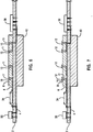
- the first dielectric layer 8 is shown attached to carrier 2 on the side opposite of stiffener 40.
- Dielectric layer 8 includes vias 10 which provide access to subsequent circuit layers and chip I/Os to circuit layer 6 of carrier 2.
- Circuit layer 6 will include input/output interconnection points that must be accessed by integrated circuit devices susbsequently placed on top of the multichip module.
- Electrically conductive material is placed in vias 10 ( Figure 6) such that electrical connection can be made from a circuit layer 12 disposed on the side of dielectric layer 8 opposite carrier 2.
- Another dielectric layer 14 is show and disposed adjacent circuit layer 12 that includes vias 16 with electrically conductive material disposed therein allowing connection between subsequent circuit layers or chip I/Os and circuit layer 12 of dielectric layer 8.
- Another layer 18 is circuitized and provided on the side of dielectric layer 14 opposite carrier 2.
- Dielectric layer 20 and subsequently formed vias 22 are shown adjacent circuit layer 18 and stacked vertically on top of dielectric layer 14. Again, electrically conductive material is placed in vias 22 to provide interconnection from another personalized circuit layer 24 placed on a side of layer 20 opposite carrier 2.
- the number of layers of dielectric material and circuit layers is determined by the complexity of the subsystem, i.e. how much wiring is required to connect the chips to each other and the other circuitry required for the subsystem.
- Electrical connection means 26 are provided on dielectric layer 20 and in communication with circuit layer 24 to provide electrical bonding with solder ball interconnect points 30, such as a C4 solder ball, of integrated circuit devices 28.
- chips 28 are electrically interconnected through each of the dielectric layers 8, 14, 20 and wiring layers 12, 18, 24 to carrier 2 and any other electronic components requiring interconnection.
- chip I/Os 30 are capable of being vertically aligned with the corresponding I/O interconnection points of the flex carrier layers 4,6 in order to reduce the area of the locally complex area (MCM) of subsystem 1 by eliminating the need for fan-out.
- MCM locally complex area
- DCA is used to attach the chips face down, as in the case of C4 attachment.
- area array footprints are also contemplated by the present invention.
- Figure 1 also shows non-complex elements 32, 34 and 36 which are placed directly on the non-complex area of flexible carrier 2, thereby reducing the required size and complexity of the locally complex area (MCM) that must be formed on flexible substrate 2.
- device 32 may be a capacitor, or the like and is shown as being interconnected to flexible carrier 2 by surface mount technology (SMT) methods.
- Pads 33 have been formed on carrier 2 and corresponding electrical connection pads on device 32 are aligned therewith and joining metallurgy, e.g. solder, is then reflowed.
- Device 34 is shown attached to the flex carrier 2 by wire bonding techniques, wherein an electrical conductor 35 is placed from an I/O on chip 34 to an electrical connection pad 37 on carrier 2.
- PTH pin through hole
- FIG. 2 a plan view is shown of flexible substrate 2 having multiple complex functional areas 1 located thereon.
- flexible substrate 2 having multiple complex functional areas 1 located thereon.
- Figure 3 shows a plan view of a single complex functional area.
- flexible carrier 2 is shown and includes non-complex electronic components 32, 34, 36, 44, shown attached thereto such as low I/O integrated circuit devices and passive devices such as capacitors and resistors.
- Interconnection means 42 are shown disposed on flexible carrier 2 which allow for carrier 2 to be interconnected with an I/O connector, or the like mounted within a computer system.
- the interconnection points 42 including pads, are used to electrically connect the flexible carrier to a printed circuit board, or the like.
- stiffener 40 is shown which may be included in the present invention depending on the thermal characteristic of the chips and material utilized.
- Interconnection points 26 are shown on the surface of the top layer of the complex area.
- Interconnection points 26 include electrically conductive pads that are compatible for joining the type of I/O interconnection points of the chip to be placed on the locally complex functional area 1.
- the I/Os 26 are electrically connected, through the previously described wiring layers, to non-complex devices 32, 34, 36, 44, carrier interconnection points 42, or one another, as shown in Figure 1 and as required for the computer function being packaged.
- FIGS 4-13 will now be used to describe a method of fabricating the present invention, as shown in Figure 1.
- flexible carrier 2 is shown with circuit layers 4 and 6 disposed on opposite sides thereof.
- Dielectric layer 8 is shown after having been placed on carrier 2 adjacent circuit layer 6 and opposite stiffener 40.
- Dielectric layer 8 consists of a photoimageable polyimide, or the like and is placed on carrier 2 by conventional means such as hot roll lamination, or the like.
- passive devices 32, 34, 36 may have been placed on carrier 2 by a previous process, or attached to the flexible carrier 2 subsequent to the completion of the locally complex functional area of the present invention.
- Passive elements 32, 34, 36 are represented on each of Figures 4-13, but it should be understood that they may be affixed to carrier 2 prior to, or after the fabrication process for the locally complex area of subsystem 1.
- vias 10 are formed in dielectric layer 8 by any one of a number of conventional methods including etching, laser ablation techniques, or the like.
- a mask is placed on top of dielectric layer 8 which is then exposed to actinic radiation, thereby removing the exposed portion of the dielectric layer 8 and forming vias 10.
- Figure 6 illustrates electrically conductive material 11 disposed within vias 10.
- conductive material 11 is electrodeposited, or plated into vias 10. Other methods such as squeeging, and the like can be used to place electrically conductive material within vias 10.
- Figure 7 shows a personalized circuit layer 12 of conductive material, e.g. copper or aluminum, formed on top of dielectric layer 8.
- This circuit layer 12 consists of a plurality of electrical signal transmission lines and allows subsequently attached ICs to be in communication with one another and other elements in the computer, e.g. other subsystems.
- a conductive seed layer of material is sputtered or otherwise placed onto the top of dielectric layer 8 to provide a base for plating conductor lines of aluminum, copper or the like onto layer 8. Additional methods of placing circuit layer 12 onto dielectric layer 8 include covering the entire surface of layer 8 with conductive metal and removing all of the metal except the desired conductive lines by etching. It should be noted that the sequence of the steps shown in Figures 5-7 can be interchanged.
- personalized circuit layer 12 may first be applied to layer 8 by methods as previously described. Subsequently, vias 10 may be formed through circuit layer 12 and dielectric 8, e.g. by etching, and conductive material 11 then added to vias 10.
- the methodology used to fabricate the present invention is not limited to the sequence of steps represented in the drawings.
- the lines of the circuit layer 12 can be formed at the same time vias 10 are filled with conductive material.
- the step of sputtering a conductive seed layer of material can be used to fill the vias, and provide the base for subsequent plating of the circuit lines of layer 12.
- the vias 10 can be filled with conductive material during the step of covering the entire surface of layer 8 with conductive material, prior to removing all of the conductive material except that required for the transmission lines of layer 12.
- the electrically conductive material 11 effectively completes the electrical connection of the flexible carrier 2 to the multichip module 1.
- interconnection points to flex carrier 2 are now provided at the top surface of the initial dielectric layer 8 of the multichip module.
- the circuit layers 4, 6 of the flex carrier 2 may form the first two circuit layers of the locally complex area, e.g. layer 12 could be considered as the third wiring layer of subsystem 1.
- a second dielectric layer 14 is then applied to the top surface of layer 8 and corresponding circuit layer 12, by means such as laminating, or the like.
- Vias 15 may then be formed, as shown in Figure 9, in dielectric layer 14 to provide a conductive path to the circuit layer 12.
- electrically conductive material 16 is shown disposed within vias 15 and another personalized circuit layer 18 of electrical transmission lines is disposed on the surface of dielectric layer 14 opposite layer 8. Again, the steps in the sequence of forming vias 15, placing circuit layer 18 on dielectric 14 and providing electrically conductive material 16 within vias 15 are interchangeable and combinable, as previously described.
- Figure 11 shows a third dielectric layer 20 placed on top of dielectric layer 14 with vias 21 formed therein corresponding to the interconnection points of circuit layer 18.
- layer 20 may be laminated to the surface of layer 14 and circuit 18, and vias 21 may be formed in layer 20 by means of etching, laser ablation, photoimaging, or the like.
- the number of layers built up in this manner is determined by the wiring density required to interconnect the chips with one another and to the flexible carrier 2.
- Figure 12 shows a circuit layer 24 placed on dielectric layer 20 by means as previously described, and electrically conductive material 22 disposed within vias 21.
- personalized circuit layer 24, disposed on the top surface of dielectric layer 20 is electrically connected with circuit layer 6 of flexible carrier 2 through vias 10, 18 ant 22.
- Interconnection points 26 include electrically conductive joining material for interfacing the chip I/Os 30, e.g solder balls, with circuit layer 24.
- Joining material 26 may include solder pads or projections, as well as electrically conductive epoxy, paste, or the like.
- the type of I/O interconnection point 26 placed on the complex area is dependent on the type of chip, or chips required to provide the function supplied by the complex area.
- Figure 13 shows the completed multichip module 1 having integrated circuit devices 28 attached to circuit layer 24 via joining means 26.
- the ICs 28 may be vertically aligned and in electrical communication with corresponding I/O interconnection points of circuit layer 6 of flex carrrier 2.
- Stiffener 40 has been removed since the manufacturing process is completed and stiffener 40 may, or may not be required due to the thermal expansion characteristics of the components.
- Protection for the chips 28 and connection pads may be provided by encapsulating chip 28 with a suitable material, such as an encapsulating epoxy.
- This encapsulation 31 will also relieve the stress on the chip I/O joints caused by difference in thermal expansion between the chip 28 and the corresponding dielectric layer, such as layer 20 ( Figure 13) and will allow removal of the stiffener 40.
- a means of packaging an entire computer function as a single unit, or subsystem that includes complex and non-complex areas has been described. These functions may include graphics capabilities, microprocessors, input/output devices, such as a keyboard, display, mouse controllers, and the like. Efficiency of the computer system is increased due to the reduced interconnection distances between integrated circuit devices. In this manner, entire computer subsystems can be efficiently manufactured and packaged, in a reduced area, on a flexible substrate, such that a computer system developer can more efficiently design new systems.
Landscapes
- Engineering & Computer Science (AREA)
- Microelectronics & Electronic Packaging (AREA)
- Physics & Mathematics (AREA)
- Condensed Matter Physics & Semiconductors (AREA)
- General Physics & Mathematics (AREA)
- Computer Hardware Design (AREA)
- Power Engineering (AREA)
- Manufacturing & Machinery (AREA)
- Structures For Mounting Electric Components On Printed Circuit Boards (AREA)
- Production Of Multi-Layered Print Wiring Board (AREA)
Applications Claiming Priority (2)
| Application Number | Priority Date | Filing Date | Title |
|---|---|---|---|
| US783644 | 1991-10-28 | ||
| US07/783,644 US5239448A (en) | 1991-10-28 | 1991-10-28 | Formulation of multichip modules |
Publications (2)
| Publication Number | Publication Date |
|---|---|
| EP0540247A2 true EP0540247A2 (fr) | 1993-05-05 |
| EP0540247A3 EP0540247A3 (en) | 1994-10-19 |
Family
ID=25129959
Family Applications (1)
| Application Number | Title | Priority Date | Filing Date |
|---|---|---|---|
| EP9292309667A Withdrawn EP0540247A3 (en) | 1991-10-28 | 1992-10-22 | Formulation of multichip modules |
Country Status (3)
| Country | Link |
|---|---|
| US (1) | US5239448A (fr) |
| EP (1) | EP0540247A3 (fr) |
| JP (1) | JPH0658941B2 (fr) |
Cited By (14)
| Publication number | Priority date | Publication date | Assignee | Title |
|---|---|---|---|---|
| EP0638931A2 (fr) * | 1993-08-12 | 1995-02-15 | Fujitsu Limited | Module à multi-puce |
| EP0642166A2 (fr) * | 1993-09-02 | 1995-03-08 | Siemens Aktiengesellschaft | Module à multichip monté sur la surface d'un circuit imprimé |
| GB2287132A (en) * | 1994-02-10 | 1995-09-06 | Matra Marconi Space France | Connecting electronic circuits in a multi-chip module having a co-fired substrate |
| EP0680082A1 (fr) * | 1993-11-12 | 1995-11-02 | Seiko Epson Corporation | Structure et procede de montage de dispositif a semi-conducteurs et dispositif d'affichage a cristaux liquides |
| FR2754416A1 (fr) * | 1996-10-04 | 1998-04-10 | Thomson Csf | Module electronique et son procede de fabrication |
| GB2337852A (en) * | 1998-05-26 | 1999-12-01 | Nec Corp | Multichip module |
| FR2781604A1 (fr) * | 1998-03-17 | 2000-01-28 | Nec Corp | Structure de carte de montage de lsi et son procede de fabrication |
| WO2001015228A1 (fr) * | 1999-08-19 | 2001-03-01 | Seiko Epson Corporation | Panneau de cablage, procede de fabrication d'un panneau de cablage, dispositif semiconducteur, procede de fabrication d'un dispositif semiconducteur, carte a circuit imprime et appareil electronique |
| CN1071535C (zh) * | 1995-09-05 | 2001-09-19 | 国际商业机器公司 | 用于在挠性电缆上安装电气元件的组合件 |
| EP1256982A1 (fr) * | 2001-05-11 | 2002-11-13 | Valtronic S.A. | Module électronique et son procede d'assemblage |
| EP1351299A3 (fr) * | 2002-04-04 | 2006-03-01 | Diehl BGT Defence GmbH & Co.KG | Construction de circuit mince at souple |
| WO2011072990A3 (fr) * | 2009-12-18 | 2011-09-15 | International Business Machines Corporation | Carte de circuits imprimés à plusieurs étages et procédé de fabrication |
| CN102328494A (zh) * | 2011-07-18 | 2012-01-25 | 吴江市锦邦纺织品有限公司 | 带可拆卸的扩展台面的印花机 |
| CN102328490A (zh) * | 2011-07-18 | 2012-01-25 | 吴江市锦邦纺织品有限公司 | 印花机的台面扩展装置 |
Families Citing this family (193)
| Publication number | Priority date | Publication date | Assignee | Title |
|---|---|---|---|---|
| US5138438A (en) * | 1987-06-24 | 1992-08-11 | Akita Electronics Co. Ltd. | Lead connections means for stacked tab packaged IC chips |
| US5399898A (en) * | 1992-07-17 | 1995-03-21 | Lsi Logic Corporation | Multi-chip semiconductor arrangements using flip chip dies |
| JPH05152509A (ja) * | 1991-11-27 | 1993-06-18 | Hitachi Ltd | 電子回路システム装置 |
| US5386342A (en) * | 1992-01-30 | 1995-01-31 | Lsi Logic Corporation | Rigid backplane formed from a moisture resistant insulative material used to protect a semiconductor device |
| FR2688629A1 (fr) * | 1992-03-10 | 1993-09-17 | Thomson Csf | Procede et dispositif d'encapsulation en trois dimensions de pastilles semi-conductrices. |
| US5397861A (en) * | 1992-10-21 | 1995-03-14 | Mupac Corporation | Electrical interconnection board |
| US5389743A (en) * | 1992-12-21 | 1995-02-14 | Hughes Aircraft Company | Rivet design for enhanced copper thick-film I/O pad adhesion |
| US5342999A (en) * | 1992-12-21 | 1994-08-30 | Motorola, Inc. | Apparatus for adapting semiconductor die pads and method therefor |
| US5378927A (en) * | 1993-05-24 | 1995-01-03 | International Business Machines Corporation | Thin-film wiring layout for a non-planar thin-film structure |
| US5485038A (en) * | 1993-07-15 | 1996-01-16 | Hughes Aircraft Company | Microelectronic circuit substrate structure including photoimageable epoxy dielectric layers |
| US5444296A (en) * | 1993-11-22 | 1995-08-22 | Sun Microsystems, Inc. | Ball grid array packages for high speed applications |
| EP0658937A1 (fr) * | 1993-12-08 | 1995-06-21 | Hughes Aircraft Company | Empilement vertical de circuits intégrés ayant des supports discrets fabriqués à partir de bandes diélectriques |
| EP0657932B1 (fr) * | 1993-12-13 | 2001-09-05 | Matsushita Electric Industrial Co., Ltd. | Assemblage avec boítier de puce et méthode de son fabrication |
| GB2288286A (en) * | 1994-03-30 | 1995-10-11 | Plessey Semiconductors Ltd | Ball grid array arrangement |
| US5579207A (en) * | 1994-10-20 | 1996-11-26 | Hughes Electronics | Three-dimensional integrated circuit stacking |
| US5715144A (en) * | 1994-12-30 | 1998-02-03 | International Business Machines Corporation | Multi-layer, multi-chip pyramid and circuit board structure |
| US5534465A (en) * | 1995-01-10 | 1996-07-09 | At&T Corp. | Method for making multichip circuits using active semiconductor substrates |
| US5798909A (en) * | 1995-02-15 | 1998-08-25 | International Business Machines Corporation | Single-tiered organic chip carriers for wire bond-type chips |
| US5635767A (en) * | 1995-06-02 | 1997-06-03 | Motorola, Inc. | Semiconductor device having built-in high frequency bypass capacitor |
| US5829124A (en) * | 1995-12-29 | 1998-11-03 | International Business Machines Corporation | Method for forming metallized patterns on the top surface of a printed circuit board |
| US5907903A (en) * | 1996-05-24 | 1999-06-01 | International Business Machines Corporation | Multi-layer-multi-chip pyramid and circuit board structure and method of forming same |
| US6667560B2 (en) | 1996-05-29 | 2003-12-23 | Texas Instruments Incorporated | Board on chip ball grid array |
| US5724230A (en) * | 1996-06-21 | 1998-03-03 | International Business Machines Corporation | Flexible laminate module including spacers embedded in an adhesive |
| US5952726A (en) * | 1996-11-12 | 1999-09-14 | Lsi Logic Corporation | Flip chip bump distribution on die |
| US5920123A (en) * | 1997-01-24 | 1999-07-06 | Micron Technology, Inc. | Multichip module assembly having via contacts and method of making the same |
| US5795299A (en) * | 1997-01-31 | 1998-08-18 | Acuson Corporation | Ultrasonic transducer assembly with extended flexible circuits |
| US6365975B1 (en) | 1997-04-02 | 2002-04-02 | Tessera, Inc. | Chip with internal signal routing in external element |
| US6188874B1 (en) | 1997-06-27 | 2001-02-13 | Lockheed Martin Corporation | Control and telemetry signal communication system for geostationary satellites |
| US6096576A (en) * | 1997-09-02 | 2000-08-01 | Silicon Light Machines | Method of producing an electrical interface to an integrated circuit device having high density I/O count |
| US6043724A (en) * | 1997-12-04 | 2000-03-28 | International Business Machines Corporation | Two-stage power noise filter with on and off chip capacitors |
| US6100113A (en) * | 1998-07-13 | 2000-08-08 | Institute Of Microelectronics | Very thin multi-chip-package and method of mass producing the same |
| US6303986B1 (en) | 1998-07-29 | 2001-10-16 | Silicon Light Machines | Method of and apparatus for sealing an hermetic lid to a semiconductor die |
| US6456502B1 (en) * | 1998-09-21 | 2002-09-24 | Compaq Computer Corporation | Integrated circuit device/circuit board connection apparatus |
| US6084779A (en) * | 1998-10-02 | 2000-07-04 | Sigrity, Inc. | Ground and power patches on printed circuit board signal planes in the areas of integrated circuit chips |
| US6329713B1 (en) * | 1998-10-21 | 2001-12-11 | International Business Machines Corporation | Integrated circuit chip carrier assembly comprising a stiffener attached to a dielectric substrate |
| US6175087B1 (en) | 1998-12-02 | 2001-01-16 | International Business Machines Corporation | Composite laminate circuit structure and method of forming the same |
| JP3162677B2 (ja) * | 1998-12-10 | 2001-05-08 | 株式会社双晶テック | 多点導電シート |
| US6163155A (en) * | 1999-01-28 | 2000-12-19 | Dresser Industries, Inc. | Electromagnetic wave resistivity tool having a tilted antenna for determining the horizontal and vertical resistivities and relative dip angle in anisotropic earth formations |
| US6476609B1 (en) * | 1999-01-28 | 2002-11-05 | Dresser Industries, Inc. | Electromagnetic wave resistivity tool having a tilted antenna for geosteering within a desired payzone |
| US7659722B2 (en) | 1999-01-28 | 2010-02-09 | Halliburton Energy Services, Inc. | Method for azimuthal resistivity measurement and bed boundary detection |
| US6274937B1 (en) * | 1999-02-01 | 2001-08-14 | Micron Technology, Inc. | Silicon multi-chip module packaging with integrated passive components and method of making |
| US6198634B1 (en) * | 1999-03-31 | 2001-03-06 | International Business Machines Corporation | Electronic package with stacked connections |
| US6569604B1 (en) | 1999-06-30 | 2003-05-27 | International Business Machines Corporation | Blind via formation in a photoimageable dielectric material |
| US6542379B1 (en) | 1999-07-15 | 2003-04-01 | International Business Machines Corporation | Circuitry with integrated passive components and method for producing |
| US20030156400A1 (en) * | 1999-07-15 | 2003-08-21 | Dibene Joseph Ted | Method and apparatus for providing power to a microprocessor with intergrated thermal and EMI management |
| US6670700B1 (en) * | 1999-08-19 | 2003-12-30 | Seiko Epson Corporation | Interconnect substrate and semiconductor device electronic instrument |
| US6777785B1 (en) | 1999-08-25 | 2004-08-17 | Winbond Electronics Corp. | Lead frame containing a master and a slave IC chips and a testing circuit embedded within the master IC chip |
| US6593645B2 (en) * | 1999-09-24 | 2003-07-15 | United Microelectronics Corp. | Three-dimensional system-on-chip structure |
| JP3973340B2 (ja) * | 1999-10-05 | 2007-09-12 | Necエレクトロニクス株式会社 | 半導体装置、配線基板、及び、それらの製造方法 |
| JP2001244391A (ja) * | 1999-12-21 | 2001-09-07 | Toyota Central Res & Dev Lab Inc | マルチチップモジュールの冷却構造 |
| US6535398B1 (en) | 2000-03-07 | 2003-03-18 | Fujitsu Limited | Multichip module substrates with buried discrete capacitors and components and methods for making |
| US6614103B1 (en) * | 2000-09-01 | 2003-09-02 | General Electric Company | Plastic packaging of LED arrays |
| TW575949B (en) | 2001-02-06 | 2004-02-11 | Hitachi Ltd | Mixed integrated circuit device, its manufacturing method and electronic apparatus |
| US6469375B2 (en) * | 2001-02-28 | 2002-10-22 | William F. Beausoleil | High bandwidth 3D memory packaging technique |
| US6987661B1 (en) | 2001-06-19 | 2006-01-17 | Amkor Technology, Inc. | Integrated circuit substrate having embedded passive components and methods therefor |
| US6930256B1 (en) | 2002-05-01 | 2005-08-16 | Amkor Technology, Inc. | Integrated circuit substrate having laser-embedded conductive patterns and method therefor |
| US7334326B1 (en) | 2001-06-19 | 2008-02-26 | Amkor Technology, Inc. | Method for making an integrated circuit substrate having embedded passive components |
| US6747781B2 (en) | 2001-06-25 | 2004-06-08 | Silicon Light Machines, Inc. | Method, apparatus, and diffuser for reducing laser speckle |
| US6782205B2 (en) | 2001-06-25 | 2004-08-24 | Silicon Light Machines | Method and apparatus for dynamic equalization in wavelength division multiplexing |
| US6829092B2 (en) | 2001-08-15 | 2004-12-07 | Silicon Light Machines, Inc. | Blazed grating light valve |
| JP3817453B2 (ja) * | 2001-09-25 | 2006-09-06 | 新光電気工業株式会社 | 半導体装置 |
| JP2003110091A (ja) * | 2001-09-28 | 2003-04-11 | Toshiba Corp | 半導体装置及び半導体装置の製造方法 |
| JP3861669B2 (ja) * | 2001-11-22 | 2006-12-20 | ソニー株式会社 | マルチチップ回路モジュールの製造方法 |
| US6800238B1 (en) | 2002-01-15 | 2004-10-05 | Silicon Light Machines, Inc. | Method for domain patterning in low coercive field ferroelectrics |
| US6831371B1 (en) | 2002-03-16 | 2004-12-14 | Amkor Technology, Inc. | Integrated circuit substrate having embedded wire conductors and method therefor |
| US7548430B1 (en) | 2002-05-01 | 2009-06-16 | Amkor Technology, Inc. | Buildup dielectric and metallization process and semiconductor package |
| US20080043447A1 (en) * | 2002-05-01 | 2008-02-21 | Amkor Technology, Inc. | Semiconductor package having laser-embedded terminals |
| US6930257B1 (en) | 2002-05-01 | 2005-08-16 | Amkor Technology, Inc. | Integrated circuit substrate having laminated laser-embedded circuit layers |
| US7633765B1 (en) | 2004-03-23 | 2009-12-15 | Amkor Technology, Inc. | Semiconductor package including a top-surface metal layer for implementing circuit features |
| US7028400B1 (en) | 2002-05-01 | 2006-04-18 | Amkor Technology, Inc. | Integrated circuit substrate having laser-exposed terminals |
| US7670962B2 (en) | 2002-05-01 | 2010-03-02 | Amkor Technology, Inc. | Substrate having stiffener fabrication method |
| US9691635B1 (en) | 2002-05-01 | 2017-06-27 | Amkor Technology, Inc. | Buildup dielectric layer having metallization pattern semiconductor package fabrication method |
| US7399661B2 (en) * | 2002-05-01 | 2008-07-15 | Amkor Technology, Inc. | Method for making an integrated circuit substrate having embedded back-side access conductors and vias |
| US6767751B2 (en) | 2002-05-28 | 2004-07-27 | Silicon Light Machines, Inc. | Integrated driver process flow |
| US6822797B1 (en) | 2002-05-31 | 2004-11-23 | Silicon Light Machines, Inc. | Light modulator structure for producing high-contrast operation using zero-order light |
| US6829258B1 (en) | 2002-06-26 | 2004-12-07 | Silicon Light Machines, Inc. | Rapidly tunable external cavity laser |
| US6714337B1 (en) | 2002-06-28 | 2004-03-30 | Silicon Light Machines | Method and device for modulating a light beam and having an improved gamma response |
| US6813059B2 (en) | 2002-06-28 | 2004-11-02 | Silicon Light Machines, Inc. | Reduced formation of asperities in contact micro-structures |
| US6700207B2 (en) * | 2002-08-05 | 2004-03-02 | Lsi Logic Corporation | Flip-chip ball grid array package for electromigration testing |
| US6801354B1 (en) | 2002-08-20 | 2004-10-05 | Silicon Light Machines, Inc. | 2-D diffraction grating for substantially eliminating polarization dependent losses |
| US6712480B1 (en) | 2002-09-27 | 2004-03-30 | Silicon Light Machines | Controlled curvature of stressed micro-structures |
| JP3925378B2 (ja) * | 2002-09-30 | 2007-06-06 | ソニー株式会社 | 高周波モジュール装置の製造方法。 |
| US6818996B2 (en) * | 2002-12-20 | 2004-11-16 | Lsi Logic Corporation | Multi-level redistribution layer traces for reducing current crowding in flipchip solder bumps |
| US6806997B1 (en) | 2003-02-28 | 2004-10-19 | Silicon Light Machines, Inc. | Patterned diffractive light modulator ribbon for PDL reduction |
| US6829077B1 (en) | 2003-02-28 | 2004-12-07 | Silicon Light Machines, Inc. | Diffractive light modulator with dynamically rotatable diffraction plane |
| US7505862B2 (en) * | 2003-03-07 | 2009-03-17 | Salmon Technologies, Llc | Apparatus and method for testing electronic systems |
| JP4203435B2 (ja) * | 2003-05-16 | 2009-01-07 | 日本特殊陶業株式会社 | 多層樹脂配線基板 |
| US7408258B2 (en) * | 2003-08-20 | 2008-08-05 | Salmon Technologies, Llc | Interconnection circuit and electronic module utilizing same |
| US7355271B2 (en) * | 2003-09-30 | 2008-04-08 | International Business Machines Corporation | Flexible assembly of stacked chips |
| JP4397210B2 (ja) * | 2003-10-20 | 2010-01-13 | ローム株式会社 | 半導体装置 |
| US20050184376A1 (en) * | 2004-02-19 | 2005-08-25 | Salmon Peter C. | System in package |
| US10811277B2 (en) | 2004-03-23 | 2020-10-20 | Amkor Technology, Inc. | Encapsulated semiconductor package |
| US11081370B2 (en) | 2004-03-23 | 2021-08-03 | Amkor Technology Singapore Holding Pte. Ltd. | Methods of manufacturing an encapsulated semiconductor device |
| US7042077B2 (en) * | 2004-04-15 | 2006-05-09 | Intel Corporation | Integrated circuit package with low modulus layer and capacitor/interposer |
| US7145238B1 (en) | 2004-05-05 | 2006-12-05 | Amkor Technology, Inc. | Semiconductor package and substrate having multi-level vias |
| US20050255722A1 (en) * | 2004-05-07 | 2005-11-17 | Salmon Peter C | Micro blade assembly |
| US7105918B2 (en) * | 2004-07-29 | 2006-09-12 | Micron Technology, Inc. | Interposer with flexible solder pad elements and methods of manufacturing the same |
| US7288726B2 (en) * | 2004-10-13 | 2007-10-30 | Chang Gung University | Hollow wire and method for making the same |
| US7427809B2 (en) * | 2004-12-16 | 2008-09-23 | Salmon Technologies, Llc | Repairable three-dimensional semiconductor subsystem |
| US20070007983A1 (en) * | 2005-01-06 | 2007-01-11 | Salmon Peter C | Semiconductor wafer tester |
| US7586192B2 (en) * | 2005-03-21 | 2009-09-08 | Intel Corporation | Routing configuration for high frequency signals in an integrated circuit package |
| US8826531B1 (en) | 2005-04-05 | 2014-09-09 | Amkor Technology, Inc. | Method for making an integrated circuit substrate having laminated laser-embedded circuit layers |
| US7586747B2 (en) | 2005-08-01 | 2009-09-08 | Salmon Technologies, Llc. | Scalable subsystem architecture having integrated cooling channels |
| US20070023923A1 (en) * | 2005-08-01 | 2007-02-01 | Salmon Peter C | Flip chip interface including a mixed array of heat bumps and signal bumps |
| US20070023904A1 (en) * | 2005-08-01 | 2007-02-01 | Salmon Peter C | Electro-optic interconnection apparatus and method |
| US20070023889A1 (en) * | 2005-08-01 | 2007-02-01 | Salmon Peter C | Copper substrate with feedthroughs and interconnection circuits |
| JP4828202B2 (ja) * | 2005-10-20 | 2011-11-30 | ルネサスエレクトロニクス株式会社 | モジュール半導体装置 |
| TWI287273B (en) * | 2006-01-25 | 2007-09-21 | Advanced Semiconductor Eng | Three dimensional package and method of making the same |
| TWI293499B (en) * | 2006-01-25 | 2008-02-11 | Advanced Semiconductor Eng | Three dimensional package and method of making the same |
| AU2006344741B2 (en) * | 2006-06-19 | 2011-07-07 | Halliburton Energy Services, Inc. | Antenna cutout in a downhole tubular |
| US7727004B2 (en) * | 2006-06-30 | 2010-06-01 | Seagate Technology Llc | Testing a high speed serial bus within a printed circuit board |
| EP2038513B1 (fr) | 2006-07-11 | 2014-05-14 | Halliburton Energy Services, Inc. | Ensemble d'outil modulaire de pilotage géologique de puits |
| EP2041607B1 (fr) * | 2006-07-12 | 2016-11-30 | Halliburton Energy Services, Inc. | Procede et appareil pour construire une antenne inclinee |
| WO2008021868A2 (fr) | 2006-08-08 | 2008-02-21 | Halliburton Energy Services, Inc. | Diagraphie de résistivité à artéfacts de pendage réduits |
| US7589398B1 (en) | 2006-10-04 | 2009-09-15 | Amkor Technology, Inc. | Embedded metal features structure |
| US7550857B1 (en) | 2006-11-16 | 2009-06-23 | Amkor Technology, Inc. | Stacked redistribution layer (RDL) die assembly package |
| CN101460698B (zh) | 2006-12-15 | 2013-01-02 | 哈里伯顿能源服务公司 | 具有旋转天线结构的天线耦合元件测量工具 |
| US7750250B1 (en) | 2006-12-22 | 2010-07-06 | Amkor Technology, Inc. | Blind via capture pad structure |
| US7752752B1 (en) | 2007-01-09 | 2010-07-13 | Amkor Technology, Inc. | Method of fabricating an embedded circuit pattern |
| GB2459067B (en) * | 2007-03-16 | 2011-11-30 | Halliburton Energy Serv Inc | Robust inversion systems and methods for azimuthally sensitive resistivity logging tools |
| KR20090007120A (ko) * | 2007-07-13 | 2009-01-16 | 삼성전자주식회사 | 봉지부를 통하여 재배선을 달성하는 웨이퍼 레벨 적층형패키지 및 그 제조방법 |
| US8323771B1 (en) | 2007-08-15 | 2012-12-04 | Amkor Technology, Inc. | Straight conductor blind via capture pad structure and fabrication method |
| US7880310B2 (en) * | 2007-09-28 | 2011-02-01 | Intel Corporation | Direct device attachment on dual-mode wirebond die |
| US10074553B2 (en) * | 2007-12-03 | 2018-09-11 | STATS ChipPAC Pte. Ltd. | Wafer level package integration and method |
| US9460951B2 (en) | 2007-12-03 | 2016-10-04 | STATS ChipPAC Pte. Ltd. | Semiconductor device and method of wafer level package integration |
| JP2009246104A (ja) * | 2008-03-31 | 2009-10-22 | Kyushu Institute Of Technology | 配線用電子部品及びその製造方法 |
| US7473618B1 (en) | 2008-04-22 | 2009-01-06 | International Business Machines Corporation | Temporary structure to reduce stress and warpage in a flip chip organic package |
| WO2010074678A2 (fr) | 2008-12-16 | 2010-07-01 | Halliburton Energy Services, Inc. | Procédés et systèmes de mesure de résistivité et de pilotage géologique azimutal au niveau du trépan |
| US8872329B1 (en) | 2009-01-09 | 2014-10-28 | Amkor Technology, Inc. | Extended landing pad substrate package structure and method |
| DE102009001461A1 (de) * | 2009-03-11 | 2010-09-16 | Robert Bosch Gmbh | Verfahren zur Herstellung einer elektronischen Baugruppe |
| US7960827B1 (en) | 2009-04-09 | 2011-06-14 | Amkor Technology, Inc. | Thermal via heat spreader package and method |
| US8623753B1 (en) | 2009-05-28 | 2014-01-07 | Amkor Technology, Inc. | Stackable protruding via package and method |
| US9930775B2 (en) * | 2009-06-02 | 2018-03-27 | Hsio Technologies, Llc | Copper pillar full metal via electrical circuit structure |
| US8222538B1 (en) | 2009-06-12 | 2012-07-17 | Amkor Technology, Inc. | Stackable via package and method |
| US8471154B1 (en) | 2009-08-06 | 2013-06-25 | Amkor Technology, Inc. | Stackable variable height via package and method |
| US8796561B1 (en) | 2009-10-05 | 2014-08-05 | Amkor Technology, Inc. | Fan out build up substrate stackable package and method |
| TWI392069B (zh) * | 2009-11-24 | 2013-04-01 | Advanced Semiconductor Eng | 封裝結構及其封裝製程 |
| US8937381B1 (en) | 2009-12-03 | 2015-01-20 | Amkor Technology, Inc. | Thin stackable package and method |
| US9691734B1 (en) | 2009-12-07 | 2017-06-27 | Amkor Technology, Inc. | Method of forming a plurality of electronic component packages |
| US8278752B2 (en) | 2009-12-23 | 2012-10-02 | Intel Corporation | Microelectronic package and method for a compression-based mid-level interconnect |
| US8536462B1 (en) | 2010-01-22 | 2013-09-17 | Amkor Technology, Inc. | Flex circuit package and method |
| BRPI1013305B1 (pt) | 2010-01-22 | 2019-09-10 | Halliburton Energy Services Inc | sistema para medir uma resistividade de uma formação, método para determinar uma resistividade,e, broca de perfuração instrumentada |
| JP5501846B2 (ja) * | 2010-05-07 | 2014-05-28 | オリンパス株式会社 | 電子デバイス、ケーブル接続構造および電子デバイスの製造方法 |
| US8300423B1 (en) | 2010-05-25 | 2012-10-30 | Amkor Technology, Inc. | Stackable treated via package and method |
| US8294276B1 (en) | 2010-05-27 | 2012-10-23 | Amkor Technology, Inc. | Semiconductor device and fabricating method thereof |
| US8338229B1 (en) | 2010-07-30 | 2012-12-25 | Amkor Technology, Inc. | Stackable plasma cleaned via package and method |
| US8717775B1 (en) | 2010-08-02 | 2014-05-06 | Amkor Technology, Inc. | Fingerprint sensor package and method |
| TWI446420B (zh) | 2010-08-27 | 2014-07-21 | Advanced Semiconductor Eng | 用於半導體製程之載體分離方法 |
| TWI445152B (zh) | 2010-08-30 | 2014-07-11 | Advanced Semiconductor Eng | 半導體結構及其製作方法 |
| US9007273B2 (en) | 2010-09-09 | 2015-04-14 | Advances Semiconductor Engineering, Inc. | Semiconductor package integrated with conformal shield and antenna |
| TWI434387B (zh) | 2010-10-11 | 2014-04-11 | Advanced Semiconductor Eng | 具有穿導孔之半導體裝置及具有穿導孔之半導體裝置之封裝結構及其製造方法 |
| US8337657B1 (en) | 2010-10-27 | 2012-12-25 | Amkor Technology, Inc. | Mechanical tape separation package and method |
| US8482134B1 (en) | 2010-11-01 | 2013-07-09 | Amkor Technology, Inc. | Stackable package and method |
| US9748154B1 (en) | 2010-11-04 | 2017-08-29 | Amkor Technology, Inc. | Wafer level fan out semiconductor device and manufacturing method thereof |
| US8525318B1 (en) | 2010-11-10 | 2013-09-03 | Amkor Technology, Inc. | Semiconductor device and fabricating method thereof |
| TWI527174B (zh) | 2010-11-19 | 2016-03-21 | 日月光半導體製造股份有限公司 | 具有半導體元件之封裝結構 |
| US8557629B1 (en) | 2010-12-03 | 2013-10-15 | Amkor Technology, Inc. | Semiconductor device having overlapped via apertures |
| US8535961B1 (en) | 2010-12-09 | 2013-09-17 | Amkor Technology, Inc. | Light emitting diode (LED) package and method |
| TWI445155B (zh) | 2011-01-06 | 2014-07-11 | Advanced Semiconductor Eng | 堆疊式封裝結構及其製造方法 |
| US8853819B2 (en) | 2011-01-07 | 2014-10-07 | Advanced Semiconductor Engineering, Inc. | Semiconductor structure with passive element network and manufacturing method thereof |
| US9721872B1 (en) | 2011-02-18 | 2017-08-01 | Amkor Technology, Inc. | Methods and structures for increasing the allowable die size in TMV packages |
| US9013011B1 (en) | 2011-03-11 | 2015-04-21 | Amkor Technology, Inc. | Stacked and staggered die MEMS package and method |
| KR101140113B1 (ko) | 2011-04-26 | 2012-04-30 | 앰코 테크놀로지 코리아 주식회사 | 반도체 디바이스 |
| US8653674B1 (en) | 2011-09-15 | 2014-02-18 | Amkor Technology, Inc. | Electronic component package fabrication method and structure |
| US8633598B1 (en) | 2011-09-20 | 2014-01-21 | Amkor Technology, Inc. | Underfill contacting stacking balls package fabrication method and structure |
| US9029962B1 (en) | 2011-10-12 | 2015-05-12 | Amkor Technology, Inc. | Molded cavity substrate MEMS package fabrication method and structure |
| US8541883B2 (en) | 2011-11-29 | 2013-09-24 | Advanced Semiconductor Engineering, Inc. | Semiconductor device having shielded conductive vias |
| US8975157B2 (en) | 2012-02-08 | 2015-03-10 | Advanced Semiconductor Engineering, Inc. | Carrier bonding and detaching processes for a semiconductor wafer |
| US8963316B2 (en) | 2012-02-15 | 2015-02-24 | Advanced Semiconductor Engineering, Inc. | Semiconductor device and method for manufacturing the same |
| US8786060B2 (en) | 2012-05-04 | 2014-07-22 | Advanced Semiconductor Engineering, Inc. | Semiconductor package integrated with conformal shield and antenna |
| BR112014030170A2 (pt) | 2012-06-25 | 2017-06-27 | Halliburton Energy Services Inc | método e sistema de perfilagem eletromagnética |
| US9153542B2 (en) | 2012-08-01 | 2015-10-06 | Advanced Semiconductor Engineering, Inc. | Semiconductor package having an antenna and manufacturing method thereof |
| US8872349B2 (en) * | 2012-09-11 | 2014-10-28 | Intel Corporation | Bridge interconnect with air gap in package assembly |
| US8937387B2 (en) | 2012-11-07 | 2015-01-20 | Advanced Semiconductor Engineering, Inc. | Semiconductor device with conductive vias |
| US8952542B2 (en) | 2012-11-14 | 2015-02-10 | Advanced Semiconductor Engineering, Inc. | Method for dicing a semiconductor wafer having through silicon vias and resultant structures |
| KR101366461B1 (ko) | 2012-11-20 | 2014-02-26 | 앰코 테크놀로지 코리아 주식회사 | 반도체 디바이스 및 그 제조 방법 |
| US9799592B2 (en) * | 2013-11-19 | 2017-10-24 | Amkor Technology, Inc. | Semicondutor device with through-silicon via-less deep wells |
| US9406552B2 (en) | 2012-12-20 | 2016-08-02 | Advanced Semiconductor Engineering, Inc. | Semiconductor device having conductive via and manufacturing process |
| US8841751B2 (en) | 2013-01-23 | 2014-09-23 | Advanced Semiconductor Engineering, Inc. | Through silicon vias for semiconductor devices and manufacturing method thereof |
| US9978688B2 (en) | 2013-02-28 | 2018-05-22 | Advanced Semiconductor Engineering, Inc. | Semiconductor package having a waveguide antenna and manufacturing method thereof |
| US9089268B2 (en) | 2013-03-13 | 2015-07-28 | Advanced Semiconductor Engineering, Inc. | Neural sensing device and method for making the same |
| US8987734B2 (en) | 2013-03-15 | 2015-03-24 | Advanced Semiconductor Engineering, Inc. | Semiconductor wafer, semiconductor process and semiconductor package |
| US9173583B2 (en) | 2013-03-15 | 2015-11-03 | Advanced Semiconductor Engineering, Inc. | Neural sensing device and method for making the same |
| KR101488590B1 (ko) | 2013-03-29 | 2015-01-30 | 앰코 테크놀로지 코리아 주식회사 | 반도체 디바이스 및 그 제조 방법 |
| KR101607981B1 (ko) | 2013-11-04 | 2016-03-31 | 앰코 테크놀로지 코리아 주식회사 | 반도체 패키지용 인터포저 및 이의 제조 방법, 제조된 인터포저를 이용한 반도체 패키지 |
| KR101982905B1 (ko) * | 2015-08-11 | 2019-05-27 | 앰코 테크놀로지 인코포레이티드 | 반도체 패키지 및 그 제조 방법 |
| KR101585554B1 (ko) * | 2014-01-22 | 2016-01-14 | 앰코 테크놀로지 코리아 주식회사 | 임베디드 트레이스 기판과 그의 범프 형성 방법 |
| US20160198072A1 (en) * | 2015-01-07 | 2016-07-07 | Magna Electronics Inc. | Pcb for camera of vehicle vision system |
| CN105990307B (zh) * | 2015-03-06 | 2019-06-07 | 恒劲科技股份有限公司 | 封装基板及包含该封装基板的封装结构及其制作方法 |
| CN106358360B (zh) * | 2015-07-14 | 2019-07-19 | 财团法人工业技术研究院 | 软性电子装置及其制造方法 |
| US9960328B2 (en) | 2016-09-06 | 2018-05-01 | Amkor Technology, Inc. | Semiconductor device and manufacturing method thereof |
| TWI701982B (zh) | 2019-05-14 | 2020-08-11 | 欣興電子股份有限公司 | 電路板結構及其製造方法 |
| CN110572927A (zh) * | 2019-08-23 | 2019-12-13 | 鹤山市中富兴业电路有限公司 | 一种多层fpc四阶hdi软硬结合板制作方法及hdi板 |
Citations (8)
| Publication number | Priority date | Publication date | Assignee | Title |
|---|---|---|---|---|
| DE2810054A1 (de) * | 1977-03-08 | 1978-09-14 | Matsushita Electric Ind Co Ltd | Elektronische schaltungsvorrichtung und verfahren zu deren herstellung |
| EP0065425A2 (fr) * | 1981-05-18 | 1982-11-24 | Matsushita Electric Industrial Co., Ltd. | Composant à circuit intégré hybride et panneau à circuit imprimé pour le montage de ce composant |
| EP0178227A2 (fr) * | 1984-10-05 | 1986-04-16 | Fujitsu Limited | Dispositif semiconducteur à circuit intégré formé sur une tranche |
| WO1987006766A1 (fr) * | 1986-05-01 | 1987-11-05 | Honeywell Inc. | Agencement d'interconnexion de plusieurs circuits integres |
| WO1988002552A1 (fr) * | 1986-09-26 | 1988-04-07 | General Electric Company | Procede et configuration de boitier de circuit integre multipuce |
| EP0337485A2 (fr) * | 1988-04-15 | 1989-10-18 | Nippon Telegraph And Telephone Corporation | Feuille de support pour circuit intégré à RF |
| EP0343379A2 (fr) * | 1988-05-26 | 1989-11-29 | International Business Machines Corporation | Empaquetage à film mince pour la connexion mixte d'une puce |
| WO1990006609A1 (fr) * | 1988-11-16 | 1990-06-14 | Motorola, Inc. | Ensemble electronique avec substrat flexible |
Family Cites Families (18)
| Publication number | Priority date | Publication date | Assignee | Title |
|---|---|---|---|---|
| US4104728A (en) * | 1973-06-06 | 1978-08-01 | Sharp Kabushiki Kaisha | Electronic apparatus equipped on a flexible substratum |
| US4177519A (en) * | 1975-07-28 | 1979-12-04 | Sharp Kabushiki Kaisha | Electronic control assembly mounted on a flexible carrier and manufacture thereof |
| US4064552A (en) * | 1976-02-03 | 1977-12-20 | Angelucci Thomas L | Multilayer flexible printed circuit tape |
| US4081898A (en) * | 1976-04-19 | 1978-04-04 | Texas Instruments Incorporated | Method of manufacturing an electronic calculator utilizing a flexible carrier |
| US4567543A (en) * | 1983-02-15 | 1986-01-28 | Motorola, Inc. | Double-sided flexible electronic circuit module |
| US4754371A (en) * | 1984-04-27 | 1988-06-28 | Nec Corporation | Large scale integrated circuit package |
| US4598337A (en) * | 1984-09-17 | 1986-07-01 | Timex Corporation | Electronic circuit board for a timepiece |
| JPH0634452B2 (ja) * | 1985-08-05 | 1994-05-02 | 株式会社日立製作所 | セラミツクス回路基板 |
| US4744008A (en) * | 1986-11-18 | 1988-05-10 | International Business Machines Corporation | Flexible film chip carrier with decoupling capacitors |
| US4990948A (en) * | 1986-12-27 | 1991-02-05 | Canon Kabushiki Kaisha | Flexible printed circuit board |
| US4843520A (en) * | 1987-02-03 | 1989-06-27 | Matsushita Electric Industrial Co. Ltd. | Electronic circuit module |
| US4933810A (en) * | 1987-04-30 | 1990-06-12 | Honeywell Inc. | Integrated circuit interconnector |
| US4926241A (en) * | 1988-02-19 | 1990-05-15 | Microelectronics And Computer Technology Corporation | Flip substrate for chip mount |
| US4987100A (en) * | 1988-05-26 | 1991-01-22 | International Business Machines Corporation | Flexible carrier for an electronic device |
| US4937707A (en) * | 1988-05-26 | 1990-06-26 | International Business Machines Corporation | Flexible carrier for an electronic device |
| US5028983A (en) * | 1988-10-28 | 1991-07-02 | International Business Machines Corporation | Multilevel integrated circuit packaging structures |
| US4982376A (en) * | 1989-04-20 | 1991-01-01 | U.S. Philips Corporation | Method of mounting electrical and/or electronic components on a single-sided printed board |
| US4967950A (en) * | 1989-10-31 | 1990-11-06 | International Business Machines Corporation | Soldering method |
-
1991
- 1991-10-28 US US07/783,644 patent/US5239448A/en not_active Expired - Fee Related
-
1992
- 1992-09-28 JP JP4258706A patent/JPH0658941B2/ja not_active Expired - Lifetime
- 1992-10-22 EP EP9292309667A patent/EP0540247A3/en not_active Withdrawn
Patent Citations (8)
| Publication number | Priority date | Publication date | Assignee | Title |
|---|---|---|---|---|
| DE2810054A1 (de) * | 1977-03-08 | 1978-09-14 | Matsushita Electric Ind Co Ltd | Elektronische schaltungsvorrichtung und verfahren zu deren herstellung |
| EP0065425A2 (fr) * | 1981-05-18 | 1982-11-24 | Matsushita Electric Industrial Co., Ltd. | Composant à circuit intégré hybride et panneau à circuit imprimé pour le montage de ce composant |
| EP0178227A2 (fr) * | 1984-10-05 | 1986-04-16 | Fujitsu Limited | Dispositif semiconducteur à circuit intégré formé sur une tranche |
| WO1987006766A1 (fr) * | 1986-05-01 | 1987-11-05 | Honeywell Inc. | Agencement d'interconnexion de plusieurs circuits integres |
| WO1988002552A1 (fr) * | 1986-09-26 | 1988-04-07 | General Electric Company | Procede et configuration de boitier de circuit integre multipuce |
| EP0337485A2 (fr) * | 1988-04-15 | 1989-10-18 | Nippon Telegraph And Telephone Corporation | Feuille de support pour circuit intégré à RF |
| EP0343379A2 (fr) * | 1988-05-26 | 1989-11-29 | International Business Machines Corporation | Empaquetage à film mince pour la connexion mixte d'une puce |
| WO1990006609A1 (fr) * | 1988-11-16 | 1990-06-14 | Motorola, Inc. | Ensemble electronique avec substrat flexible |
Cited By (25)
| Publication number | Priority date | Publication date | Assignee | Title |
|---|---|---|---|---|
| EP0638931A3 (fr) * | 1993-08-12 | 1995-05-10 | Fujitsu Ltd | Module à multi-puce. |
| EP0638931A2 (fr) * | 1993-08-12 | 1995-02-15 | Fujitsu Limited | Module à multi-puce |
| US5586006A (en) * | 1993-08-12 | 1996-12-17 | Fujitsu Limited | Multi-chip module having a multi-layer circuit board with insulating layers and wiring conductors stacked together |
| US6154372A (en) * | 1993-09-02 | 2000-11-28 | Siemens Aktiengesellschaft | Multichip module for surface mounting on printed circuit boards |
| EP0642166A3 (fr) * | 1993-09-02 | 1995-04-05 | Siemens Ag | |
| EP0642166A2 (fr) * | 1993-09-02 | 1995-03-08 | Siemens Aktiengesellschaft | Module à multichip monté sur la surface d'un circuit imprimé |
| EP0680082A1 (fr) * | 1993-11-12 | 1995-11-02 | Seiko Epson Corporation | Structure et procede de montage de dispositif a semi-conducteurs et dispositif d'affichage a cristaux liquides |
| EP0680082A4 (fr) * | 1993-11-12 | 1997-04-02 | Seiko Epson Corp | Structure et procede de montage de dispositif a semi-conducteurs et dispositif d'affichage a cristaux liquides. |
| GB2287132A (en) * | 1994-02-10 | 1995-09-06 | Matra Marconi Space France | Connecting electronic circuits in a multi-chip module having a co-fired substrate |
| GB2287132B (en) * | 1994-02-10 | 1997-10-15 | Matra Marconi Space France | A method for connecting electronic circuits in a multi-chip module having a co-fired substrate, and multi-chip module obtained thereby |
| CN1071535C (zh) * | 1995-09-05 | 2001-09-19 | 国际商业机器公司 | 用于在挠性电缆上安装电气元件的组合件 |
| FR2754416A1 (fr) * | 1996-10-04 | 1998-04-10 | Thomson Csf | Module electronique et son procede de fabrication |
| FR2781604A1 (fr) * | 1998-03-17 | 2000-01-28 | Nec Corp | Structure de carte de montage de lsi et son procede de fabrication |
| US6285559B1 (en) | 1998-05-26 | 2001-09-04 | Nec Corporation | Multichip module |
| GB2337852A (en) * | 1998-05-26 | 1999-12-01 | Nec Corp | Multichip module |
| GB2337852B (en) * | 1998-05-26 | 2002-11-20 | Nec Corp | Multichip Module |
| WO2001015228A1 (fr) * | 1999-08-19 | 2001-03-01 | Seiko Epson Corporation | Panneau de cablage, procede de fabrication d'un panneau de cablage, dispositif semiconducteur, procede de fabrication d'un dispositif semiconducteur, carte a circuit imprime et appareil electronique |
| US6977441B2 (en) | 1999-08-19 | 2005-12-20 | Seiko Epson Corporation | Interconnect substrate and method of manufacture thereof, electronic component and method of manufacturing thereof, circuit board and electronic instrument |
| EP1256982A1 (fr) * | 2001-05-11 | 2002-11-13 | Valtronic S.A. | Module électronique et son procede d'assemblage |
| WO2002093649A2 (fr) * | 2001-05-11 | 2002-11-21 | Valtronic S.A. | Module electronique et son procede d'assemblage |
| WO2002093649A3 (fr) * | 2001-05-11 | 2003-05-30 | Valtronic S A | Module electronique et son procede d'assemblage |
| EP1351299A3 (fr) * | 2002-04-04 | 2006-03-01 | Diehl BGT Defence GmbH & Co.KG | Construction de circuit mince at souple |
| WO2011072990A3 (fr) * | 2009-12-18 | 2011-09-15 | International Business Machines Corporation | Carte de circuits imprimés à plusieurs étages et procédé de fabrication |
| CN102328494A (zh) * | 2011-07-18 | 2012-01-25 | 吴江市锦邦纺织品有限公司 | 带可拆卸的扩展台面的印花机 |
| CN102328490A (zh) * | 2011-07-18 | 2012-01-25 | 吴江市锦邦纺织品有限公司 | 印花机的台面扩展装置 |
Also Published As
| Publication number | Publication date |
|---|---|
| EP0540247A3 (en) | 1994-10-19 |
| JPH0658941B2 (ja) | 1994-08-03 |
| JPH05218287A (ja) | 1993-08-27 |
| US5239448A (en) | 1993-08-24 |
Similar Documents
| Publication | Publication Date | Title |
|---|---|---|
| US5239448A (en) | Formulation of multichip modules | |
| US5198965A (en) | Free form packaging of specific functions within a computer system | |
| US5229916A (en) | Chip edge interconnect overlay element | |
| EP0527044B1 (fr) | Empaquetage pour mémoire | |
| US5039628A (en) | Flip substrate for chip mount | |
| US4926241A (en) | Flip substrate for chip mount | |
| US5343366A (en) | Packages for stacked integrated circuit chip cubes | |
| EP0729180B1 (fr) | Empaquetage de modules à multi-puces sans interconnexion à fil | |
| EP0072673B1 (fr) | Film support à conducteurs pour l'interconnexion électrique entre des composants électroniques et un circuit externe | |
| US6889429B2 (en) | Method of making a lead-free integrated circuit package | |
| US6495912B1 (en) | Structure of ceramic package with integrated passive devices | |
| US6081026A (en) | High density signal interposer with power and ground wrap | |
| EP0653789A2 (fr) | Structure de boîtier électronique et sa fabrication | |
| EP0460822A1 (fr) | Unité de circuit intégré utilisant un substrat flexible | |
| EP0624905A1 (fr) | Module multi-puces | |
| US20060105500A1 (en) | Process for fabricating chip embedded package structure | |
| JP2000164765A (ja) | 電源及び接地ラップを具備したクロスト―クノイズ低減形の高密度信号介挿体、並びに、介挿体の製造方法 | |
| US6528734B2 (en) | Semiconductor device and process for fabricating the same | |
| JPH07201902A (ja) | マンドレルで製造した相互接続デカールを有するマルチチップモジュール | |
| JP3247634B2 (ja) | 半導体デバイス・パッケージ及び組み立て方法 | |
| US6256207B1 (en) | Chip-sized semiconductor device and process for making same | |
| US5184284A (en) | Method and apparatus for implementing engineering changes for integrated circuit module | |
| US6562656B1 (en) | Cavity down flip chip BGA | |
| EP0521720A1 (fr) | Circuit imprimé multicouche dissipant la chaleur | |
| JPH01256161A (ja) | 印刷配線板装置 |
Legal Events
| Date | Code | Title | Description |
|---|---|---|---|
| PUAI | Public reference made under article 153(3) epc to a published international application that has entered the european phase |
Free format text: ORIGINAL CODE: 0009012 |
|
| AK | Designated contracting states |
Kind code of ref document: A2 Designated state(s): DE FR GB |
|
| 17P | Request for examination filed |
Effective date: 19930819 |
|
| PUAL | Search report despatched |
Free format text: ORIGINAL CODE: 0009013 |
|
| AK | Designated contracting states |
Kind code of ref document: A3 Designated state(s): DE FR GB |
|
| 17Q | First examination report despatched |
Effective date: 19950623 |
|
| STAA | Information on the status of an ep patent application or granted ep patent |
Free format text: STATUS: THE APPLICATION IS DEEMED TO BE WITHDRAWN |
|
| 18D | Application deemed to be withdrawn |
Effective date: 19960104 |