EP0530003B1 - Resistive metal layers and method for making same - Google Patents
Resistive metal layers and method for making same Download PDFInfo
- Publication number
- EP0530003B1 EP0530003B1 EP92307753A EP92307753A EP0530003B1 EP 0530003 B1 EP0530003 B1 EP 0530003B1 EP 92307753 A EP92307753 A EP 92307753A EP 92307753 A EP92307753 A EP 92307753A EP 0530003 B1 EP0530003 B1 EP 0530003B1
- Authority
- EP
- European Patent Office
- Prior art keywords
- layer
- resistive
- conductive
- atom
- laminate
- Prior art date
- Legal status (The legal status is an assumption and is not a legal conclusion. Google has not performed a legal analysis and makes no representation as to the accuracy of the status listed.)
- Expired - Lifetime
Links
- 229910052751 metal Inorganic materials 0.000 title claims abstract description 51
- 239000002184 metal Substances 0.000 title claims abstract description 51
- 238000000034 method Methods 0.000 title claims description 50
- 239000000654 additive Substances 0.000 claims abstract description 35
- 230000000996 additive effect Effects 0.000 claims abstract description 33
- 238000009713 electroplating Methods 0.000 claims abstract description 30
- VYZAMTAEIAYCRO-UHFFFAOYSA-N Chromium Chemical compound [Cr] VYZAMTAEIAYCRO-UHFFFAOYSA-N 0.000 claims description 58
- 239000011888 foil Substances 0.000 claims description 56
- 239000011651 chromium Substances 0.000 claims description 53
- 229910052804 chromium Inorganic materials 0.000 claims description 52
- QTBSBXVTEAMEQO-UHFFFAOYSA-N Acetic acid Chemical compound CC(O)=O QTBSBXVTEAMEQO-UHFFFAOYSA-N 0.000 claims description 48
- IJGRMHOSHXDMSA-UHFFFAOYSA-N Atomic nitrogen Chemical compound N#N IJGRMHOSHXDMSA-UHFFFAOYSA-N 0.000 claims description 44
- PXHVJJICTQNCMI-UHFFFAOYSA-N Nickel Chemical compound [Ni] PXHVJJICTQNCMI-UHFFFAOYSA-N 0.000 claims description 43
- RYGMFSIKBFXOCR-UHFFFAOYSA-N Copper Chemical compound [Cu] RYGMFSIKBFXOCR-UHFFFAOYSA-N 0.000 claims description 41
- OKTJSMMVPCPJKN-UHFFFAOYSA-N Carbon Chemical compound [C] OKTJSMMVPCPJKN-UHFFFAOYSA-N 0.000 claims description 37
- 229910052799 carbon Inorganic materials 0.000 claims description 37
- 238000007747 plating Methods 0.000 claims description 31
- VEXZGXHMUGYJMC-UHFFFAOYSA-N Hydrochloric acid Chemical compound Cl VEXZGXHMUGYJMC-UHFFFAOYSA-N 0.000 claims description 24
- 239000011889 copper foil Substances 0.000 claims description 23
- 239000002131 composite material Substances 0.000 claims description 22
- 229910052757 nitrogen Inorganic materials 0.000 claims description 22
- 229910052759 nickel Inorganic materials 0.000 claims description 21
- ORTQZVOHEJQUHG-UHFFFAOYSA-L copper(II) chloride Chemical compound Cl[Cu]Cl ORTQZVOHEJQUHG-UHFFFAOYSA-L 0.000 claims description 20
- 238000005530 etching Methods 0.000 claims description 20
- -1 alkali metal salt Chemical class 0.000 claims description 19
- ZOKXTWBITQBERF-UHFFFAOYSA-N Molybdenum Chemical compound [Mo] ZOKXTWBITQBERF-UHFFFAOYSA-N 0.000 claims description 18
- OAICVXFJPJFONN-UHFFFAOYSA-N Phosphorus Chemical compound [P] OAICVXFJPJFONN-UHFFFAOYSA-N 0.000 claims description 18
- 229910052802 copper Inorganic materials 0.000 claims description 18
- 239000010949 copper Substances 0.000 claims description 18
- 229910052750 molybdenum Inorganic materials 0.000 claims description 18
- 239000011733 molybdenum Substances 0.000 claims description 18
- 229910052698 phosphorus Inorganic materials 0.000 claims description 18
- 239000011574 phosphorus Substances 0.000 claims description 18
- WFKWXMTUELFFGS-UHFFFAOYSA-N tungsten Chemical compound [W] WFKWXMTUELFFGS-UHFFFAOYSA-N 0.000 claims description 18
- 229910052721 tungsten Inorganic materials 0.000 claims description 18
- 239000010937 tungsten Substances 0.000 claims description 18
- QVGXLLKOCUKJST-UHFFFAOYSA-N atomic oxygen Chemical compound [O] QVGXLLKOCUKJST-UHFFFAOYSA-N 0.000 claims description 15
- 229910052760 oxygen Inorganic materials 0.000 claims description 15
- 239000001301 oxygen Substances 0.000 claims description 15
- 229910017052 cobalt Inorganic materials 0.000 claims description 14
- 239000010941 cobalt Substances 0.000 claims description 14
- GUTLYIVDDKVIGB-UHFFFAOYSA-N cobalt atom Chemical compound [Co] GUTLYIVDDKVIGB-UHFFFAOYSA-N 0.000 claims description 14
- XBDQKXXYIPTUBI-UHFFFAOYSA-N dimethylselenoniopropionate Natural products CCC(O)=O XBDQKXXYIPTUBI-UHFFFAOYSA-N 0.000 claims description 14
- 239000002253 acid Substances 0.000 claims description 13
- 229910052720 vanadium Inorganic materials 0.000 claims description 12
- 229960003280 cupric chloride Drugs 0.000 claims description 9
- 238000004519 manufacturing process Methods 0.000 claims description 9
- MHAJPDPJQMAIIY-UHFFFAOYSA-N Hydrogen peroxide Chemical compound OO MHAJPDPJQMAIIY-UHFFFAOYSA-N 0.000 claims description 7
- 230000000873 masking effect Effects 0.000 claims description 7
- 235000019260 propionic acid Nutrition 0.000 claims description 7
- IUVKMZGDUIUOCP-BTNSXGMBSA-N quinbolone Chemical compound O([C@H]1CC[C@H]2[C@H]3[C@@H]([C@]4(C=CC(=O)C=C4CC3)C)CC[C@@]21C)C1=CCCC1 IUVKMZGDUIUOCP-BTNSXGMBSA-N 0.000 claims description 6
- 239000007864 aqueous solution Substances 0.000 claims description 5
- BHEPBYXIRTUNPN-UHFFFAOYSA-N hydridophosphorus(.) (triplet) Chemical compound [PH] BHEPBYXIRTUNPN-UHFFFAOYSA-N 0.000 claims description 5
- KDLHZDBZIXYQEI-UHFFFAOYSA-N Palladium Chemical compound [Pd] KDLHZDBZIXYQEI-UHFFFAOYSA-N 0.000 claims description 4
- RBTARNINKXHZNM-UHFFFAOYSA-K iron trichloride Chemical compound Cl[Fe](Cl)Cl RBTARNINKXHZNM-UHFFFAOYSA-K 0.000 claims description 4
- BDAGIHXWWSANSR-UHFFFAOYSA-N methanoic acid Natural products OC=O BDAGIHXWWSANSR-UHFFFAOYSA-N 0.000 claims description 4
- BASFCYQUMIYNBI-UHFFFAOYSA-N platinum Chemical compound [Pt] BASFCYQUMIYNBI-UHFFFAOYSA-N 0.000 claims description 4
- RTAQQCXQSZGOHL-UHFFFAOYSA-N Titanium Chemical compound [Ti] RTAQQCXQSZGOHL-UHFFFAOYSA-N 0.000 claims description 3
- 229910052719 titanium Inorganic materials 0.000 claims description 3
- 239000010936 titanium Substances 0.000 claims description 3
- OSWFIVFLDKOXQC-UHFFFAOYSA-N 4-(3-methoxyphenyl)aniline Chemical compound COC1=CC=CC(C=2C=CC(N)=CC=2)=C1 OSWFIVFLDKOXQC-UHFFFAOYSA-N 0.000 claims description 2
- 229910052684 Cerium Inorganic materials 0.000 claims description 2
- 229910021578 Iron(III) chloride Inorganic materials 0.000 claims description 2
- KJTLSVCANCCWHF-UHFFFAOYSA-N Ruthenium Chemical compound [Ru] KJTLSVCANCCWHF-UHFFFAOYSA-N 0.000 claims description 2
- BQCADISMDOOEFD-UHFFFAOYSA-N Silver Chemical compound [Ag] BQCADISMDOOEFD-UHFFFAOYSA-N 0.000 claims description 2
- QCWXUUIWCKQGHC-UHFFFAOYSA-N Zirconium Chemical compound [Zr] QCWXUUIWCKQGHC-UHFFFAOYSA-N 0.000 claims description 2
- 235000011054 acetic acid Nutrition 0.000 claims description 2
- 229910052783 alkali metal Inorganic materials 0.000 claims description 2
- 235000019253 formic acid Nutrition 0.000 claims description 2
- 229910052758 niobium Inorganic materials 0.000 claims description 2
- 239000010955 niobium Substances 0.000 claims description 2
- GUCVJGMIXFAOAE-UHFFFAOYSA-N niobium atom Chemical compound [Nb] GUCVJGMIXFAOAE-UHFFFAOYSA-N 0.000 claims description 2
- 229910052763 palladium Inorganic materials 0.000 claims description 2
- 229910052697 platinum Inorganic materials 0.000 claims description 2
- 229910052707 ruthenium Inorganic materials 0.000 claims description 2
- 229910052706 scandium Inorganic materials 0.000 claims description 2
- SIXSYDAISGFNSX-UHFFFAOYSA-N scandium atom Chemical compound [Sc] SIXSYDAISGFNSX-UHFFFAOYSA-N 0.000 claims description 2
- 229910052709 silver Inorganic materials 0.000 claims description 2
- 239000004332 silver Substances 0.000 claims description 2
- 229910052715 tantalum Inorganic materials 0.000 claims description 2
- GUVRBAGPIYLISA-UHFFFAOYSA-N tantalum atom Chemical compound [Ta] GUVRBAGPIYLISA-UHFFFAOYSA-N 0.000 claims description 2
- 229910052727 yttrium Inorganic materials 0.000 claims description 2
- VWQVUPCCIRVNHF-UHFFFAOYSA-N yttrium atom Chemical compound [Y] VWQVUPCCIRVNHF-UHFFFAOYSA-N 0.000 claims description 2
- 229910052726 zirconium Inorganic materials 0.000 claims description 2
- LEONUFNNVUYDNQ-UHFFFAOYSA-N vanadium atom Chemical compound [V] LEONUFNNVUYDNQ-UHFFFAOYSA-N 0.000 claims 4
- GWXLDORMOJMVQZ-UHFFFAOYSA-N cerium Chemical compound [Ce] GWXLDORMOJMVQZ-UHFFFAOYSA-N 0.000 claims 1
- 238000002360 preparation method Methods 0.000 abstract description 2
- QAOWNCQODCNURD-UHFFFAOYSA-N Sulfuric acid Chemical compound OS(O)(=O)=O QAOWNCQODCNURD-UHFFFAOYSA-N 0.000 description 39
- 239000000463 material Substances 0.000 description 33
- WGLPBDUCMAPZCE-UHFFFAOYSA-N chromium trioxide Inorganic materials O=[Cr](=O)=O WGLPBDUCMAPZCE-UHFFFAOYSA-N 0.000 description 24
- 229920002120 photoresistant polymer Polymers 0.000 description 22
- 239000000243 solution Substances 0.000 description 22
- 125000004429 atom Chemical group 0.000 description 19
- 239000000203 mixture Substances 0.000 description 19
- 239000000758 substrate Substances 0.000 description 16
- KRVSOGSZCMJSLX-UHFFFAOYSA-L chromic acid Substances O[Cr](O)(=O)=O KRVSOGSZCMJSLX-UHFFFAOYSA-L 0.000 description 14
- 239000004020 conductor Substances 0.000 description 14
- 230000000694 effects Effects 0.000 description 14
- AWJWCTOOIBYHON-UHFFFAOYSA-N furo[3,4-b]pyrazine-5,7-dione Chemical compound C1=CN=C2C(=O)OC(=O)C2=N1 AWJWCTOOIBYHON-UHFFFAOYSA-N 0.000 description 12
- 238000000151 deposition Methods 0.000 description 11
- 230000008021 deposition Effects 0.000 description 11
- 238000009472 formulation Methods 0.000 description 11
- 150000003839 salts Chemical class 0.000 description 11
- 239000004615 ingredient Substances 0.000 description 9
- 150000002739 metals Chemical class 0.000 description 9
- 239000000126 substance Substances 0.000 description 9
- 150000001450 anions Chemical class 0.000 description 8
- 239000003054 catalyst Substances 0.000 description 8
- XTEGARKTQYYJKE-UHFFFAOYSA-M chlorate Inorganic materials [O-]Cl(=O)=O XTEGARKTQYYJKE-UHFFFAOYSA-M 0.000 description 8
- GPPXJZIENCGNKB-UHFFFAOYSA-N vanadium Chemical compound [V]#[V] GPPXJZIENCGNKB-UHFFFAOYSA-N 0.000 description 8
- QAOWNCQODCNURD-UHFFFAOYSA-L Sulfate Chemical compound [O-]S([O-])(=O)=O QAOWNCQODCNURD-UHFFFAOYSA-L 0.000 description 7
- 150000007524 organic acids Chemical class 0.000 description 7
- 229910045601 alloy Inorganic materials 0.000 description 6
- 239000000956 alloy Substances 0.000 description 6
- 238000004458 analytical method Methods 0.000 description 6
- 150000001875 compounds Chemical class 0.000 description 6
- 230000008878 coupling Effects 0.000 description 6
- 238000010168 coupling process Methods 0.000 description 6
- 238000005859 coupling reaction Methods 0.000 description 6
- BZSXEZOLBIJVQK-UHFFFAOYSA-N 2-methylsulfonylbenzoic acid Chemical compound CS(=O)(=O)C1=CC=CC=C1C(O)=O BZSXEZOLBIJVQK-UHFFFAOYSA-N 0.000 description 5
- 239000002482 conductive additive Substances 0.000 description 5
- NBIIXXVUZAFLBC-UHFFFAOYSA-N Phosphoric acid Chemical compound OP(O)(O)=O NBIIXXVUZAFLBC-UHFFFAOYSA-N 0.000 description 4
- 150000007513 acids Chemical class 0.000 description 4
- 239000013590 bulk material Substances 0.000 description 4
- 239000013078 crystal Substances 0.000 description 4
- 230000007423 decrease Effects 0.000 description 4
- 238000004070 electrodeposition Methods 0.000 description 4
- 238000005516 engineering process Methods 0.000 description 4
- 125000001475 halogen functional group Chemical group 0.000 description 4
- 150000002894 organic compounds Chemical class 0.000 description 4
- LLYCMZGLHLKPPU-UHFFFAOYSA-M perbromate Chemical compound [O-]Br(=O)(=O)=O LLYCMZGLHLKPPU-UHFFFAOYSA-M 0.000 description 4
- 239000002243 precursor Substances 0.000 description 4
- 230000008569 process Effects 0.000 description 4
- 238000003860 storage Methods 0.000 description 4
- 229910052717 sulfur Inorganic materials 0.000 description 4
- NINIDFKCEFEMDL-UHFFFAOYSA-N Sulfur Chemical compound [S] NINIDFKCEFEMDL-UHFFFAOYSA-N 0.000 description 3
- XSQUKJJJFZCRTK-UHFFFAOYSA-N Urea Natural products NC(N)=O XSQUKJJJFZCRTK-UHFFFAOYSA-N 0.000 description 3
- 238000013019 agitation Methods 0.000 description 3
- SXDBWCPKPHAZSM-UHFFFAOYSA-M bromate Inorganic materials [O-]Br(=O)=O SXDBWCPKPHAZSM-UHFFFAOYSA-M 0.000 description 3
- SXDBWCPKPHAZSM-UHFFFAOYSA-N bromic acid Chemical compound OBr(=O)=O SXDBWCPKPHAZSM-UHFFFAOYSA-N 0.000 description 3
- 210000004027 cell Anatomy 0.000 description 3
- KRKNYBCHXYNGOX-UHFFFAOYSA-N citric acid Chemical compound OC(=O)CC(O)(C(O)=O)CC(O)=O KRKNYBCHXYNGOX-UHFFFAOYSA-N 0.000 description 3
- 238000000354 decomposition reaction Methods 0.000 description 3
- QJGQUHMNIGDVPM-UHFFFAOYSA-N nitrogen group Chemical group [N] QJGQUHMNIGDVPM-UHFFFAOYSA-N 0.000 description 3
- 239000000047 product Substances 0.000 description 3
- 239000011593 sulfur Substances 0.000 description 3
- DHMQDGOQFOQNFH-UHFFFAOYSA-N Glycine Chemical compound NCC(O)=O DHMQDGOQFOQNFH-UHFFFAOYSA-N 0.000 description 2
- DGAQECJNVWCQMB-PUAWFVPOSA-M Ilexoside XXIX Chemical compound C[C@@H]1CC[C@@]2(CC[C@@]3(C(=CC[C@H]4[C@]3(CC[C@@H]5[C@@]4(CC[C@@H](C5(C)C)OS(=O)(=O)[O-])C)C)[C@@H]2[C@]1(C)O)C)C(=O)O[C@H]6[C@@H]([C@H]([C@@H]([C@H](O6)CO)O)O)O.[Na+] DGAQECJNVWCQMB-PUAWFVPOSA-M 0.000 description 2
- 229910002651 NO3 Inorganic materials 0.000 description 2
- 238000002441 X-ray diffraction Methods 0.000 description 2
- YDONNITUKPKTIG-UHFFFAOYSA-N [Nitrilotris(methylene)]trisphosphonic acid Chemical compound OP(O)(=O)CN(CP(O)(O)=O)CP(O)(O)=O YDONNITUKPKTIG-UHFFFAOYSA-N 0.000 description 2
- 230000032683 aging Effects 0.000 description 2
- 239000003570 air Substances 0.000 description 2
- 229910000147 aluminium phosphate Inorganic materials 0.000 description 2
- 150000001412 amines Chemical group 0.000 description 2
- 229910052787 antimony Inorganic materials 0.000 description 2
- WATWJIUSRGPENY-UHFFFAOYSA-N antimony atom Chemical compound [Sb] WATWJIUSRGPENY-UHFFFAOYSA-N 0.000 description 2
- 238000013459 approach Methods 0.000 description 2
- 229910002056 binary alloy Inorganic materials 0.000 description 2
- 230000015572 biosynthetic process Effects 0.000 description 2
- 125000004432 carbon atom Chemical group C* 0.000 description 2
- 239000003153 chemical reaction reagent Substances 0.000 description 2
- 238000002485 combustion reaction Methods 0.000 description 2
- 239000008139 complexing agent Substances 0.000 description 2
- 238000011109 contamination Methods 0.000 description 2
- 230000003247 decreasing effect Effects 0.000 description 2
- 238000013461 design Methods 0.000 description 2
- 238000011161 development Methods 0.000 description 2
- 230000018109 developmental process Effects 0.000 description 2
- 238000009826 distribution Methods 0.000 description 2
- GNTDGMZSJNCJKK-UHFFFAOYSA-N divanadium pentaoxide Chemical compound O=[V](=O)O[V](=O)=O GNTDGMZSJNCJKK-UHFFFAOYSA-N 0.000 description 2
- 230000005611 electricity Effects 0.000 description 2
- 239000002659 electrodeposit Substances 0.000 description 2
- 239000004744 fabric Substances 0.000 description 2
- 239000011152 fibreglass Substances 0.000 description 2
- 210000002287 horizontal cell Anatomy 0.000 description 2
- 239000012535 impurity Substances 0.000 description 2
- ICIWUVCWSCSTAQ-UHFFFAOYSA-M iodate Chemical compound [O-]I(=O)=O ICIWUVCWSCSTAQ-UHFFFAOYSA-M 0.000 description 2
- VLAPMBHFAWRUQP-UHFFFAOYSA-L molybdic acid Chemical compound O[Mo](O)(=O)=O VLAPMBHFAWRUQP-UHFFFAOYSA-L 0.000 description 2
- 229910000008 nickel(II) carbonate Inorganic materials 0.000 description 2
- ZULUUIKRFGGGTL-UHFFFAOYSA-L nickel(ii) carbonate Chemical compound [Ni+2].[O-]C([O-])=O ZULUUIKRFGGGTL-UHFFFAOYSA-L 0.000 description 2
- 229910052755 nonmetal Inorganic materials 0.000 description 2
- 230000003647 oxidation Effects 0.000 description 2
- 238000007254 oxidation reaction Methods 0.000 description 2
- VLTRZXGMWDSKGL-UHFFFAOYSA-M perchlorate Inorganic materials [O-]Cl(=O)(=O)=O VLTRZXGMWDSKGL-UHFFFAOYSA-M 0.000 description 2
- VLTRZXGMWDSKGL-UHFFFAOYSA-N perchloric acid Chemical compound OCl(=O)(=O)=O VLTRZXGMWDSKGL-UHFFFAOYSA-N 0.000 description 2
- KHIWWQKSHDUIBK-UHFFFAOYSA-N periodic acid Chemical compound OI(=O)(=O)=O KHIWWQKSHDUIBK-UHFFFAOYSA-N 0.000 description 2
- 229920006267 polyester film Polymers 0.000 description 2
- 238000012545 processing Methods 0.000 description 2
- 239000011347 resin Substances 0.000 description 2
- 229920005989 resin Polymers 0.000 description 2
- 229910052708 sodium Inorganic materials 0.000 description 2
- 239000011734 sodium Substances 0.000 description 2
- ISIJQEHRDSCQIU-UHFFFAOYSA-N tert-butyl 2,7-diazaspiro[4.5]decane-7-carboxylate Chemical compound C1N(C(=O)OC(C)(C)C)CCCC11CNCC1 ISIJQEHRDSCQIU-UHFFFAOYSA-N 0.000 description 2
- UMGDCJDMYOKAJW-UHFFFAOYSA-N thiourea Chemical compound NC(N)=S UMGDCJDMYOKAJW-UHFFFAOYSA-N 0.000 description 2
- CMPGARWFYBADJI-UHFFFAOYSA-L tungstic acid Chemical compound O[W](O)(=O)=O CMPGARWFYBADJI-UHFFFAOYSA-L 0.000 description 2
- XLYOFNOQVPJJNP-UHFFFAOYSA-N water Substances O XLYOFNOQVPJJNP-UHFFFAOYSA-N 0.000 description 2
- ZSLUVFAKFWKJRC-IGMARMGPSA-N 232Th Chemical compound [232Th] ZSLUVFAKFWKJRC-IGMARMGPSA-N 0.000 description 1
- YCPXWRQRBFJBPZ-UHFFFAOYSA-N 5-sulfosalicylic acid Chemical compound OC(=O)C1=CC(S(O)(=O)=O)=CC=C1O YCPXWRQRBFJBPZ-UHFFFAOYSA-N 0.000 description 1
- 239000004593 Epoxy Substances 0.000 description 1
- BDAGIHXWWSANSR-UHFFFAOYSA-M Formate Chemical compound [O-]C=O BDAGIHXWWSANSR-UHFFFAOYSA-M 0.000 description 1
- 108010010803 Gelatin Proteins 0.000 description 1
- 239000004471 Glycine Substances 0.000 description 1
- UFHFLCQGNIYNRP-UHFFFAOYSA-N Hydrogen Chemical compound [H][H] UFHFLCQGNIYNRP-UHFFFAOYSA-N 0.000 description 1
- CKLJMWTZIZZHCS-REOHCLBHSA-N L-aspartic acid Chemical compound OC(=O)[C@@H](N)CC(O)=O CKLJMWTZIZZHCS-REOHCLBHSA-N 0.000 description 1
- PWHULOQIROXLJO-UHFFFAOYSA-N Manganese Chemical compound [Mn] PWHULOQIROXLJO-UHFFFAOYSA-N 0.000 description 1
- NHNBFGGVMKEFGY-UHFFFAOYSA-N Nitrate Chemical compound [O-][N+]([O-])=O NHNBFGGVMKEFGY-UHFFFAOYSA-N 0.000 description 1
- GRYLNZFGIOXLOG-UHFFFAOYSA-N Nitric acid Chemical compound O[N+]([O-])=O GRYLNZFGIOXLOG-UHFFFAOYSA-N 0.000 description 1
- 229910019142 PO4 Inorganic materials 0.000 description 1
- 229910001245 Sb alloy Inorganic materials 0.000 description 1
- XUIMIQQOPSSXEZ-UHFFFAOYSA-N Silicon Chemical compound [Si] XUIMIQQOPSSXEZ-UHFFFAOYSA-N 0.000 description 1
- 229910052776 Thorium Inorganic materials 0.000 description 1
- 230000001464 adherent effect Effects 0.000 description 1
- 239000000853 adhesive Substances 0.000 description 1
- 230000001070 adhesive effect Effects 0.000 description 1
- 230000002411 adverse Effects 0.000 description 1
- 125000001931 aliphatic group Chemical group 0.000 description 1
- 239000012080 ambient air Substances 0.000 description 1
- 235000001014 amino acid Nutrition 0.000 description 1
- 150000001413 amino acids Chemical class 0.000 description 1
- 238000002048 anodisation reaction Methods 0.000 description 1
- 239000002140 antimony alloy Substances 0.000 description 1
- 239000012736 aqueous medium Substances 0.000 description 1
- 235000003704 aspartic acid Nutrition 0.000 description 1
- 239000012298 atmosphere Substances 0.000 description 1
- 238000001479 atomic absorption spectroscopy Methods 0.000 description 1
- OQFSQFPPLPISGP-UHFFFAOYSA-N beta-carboxyaspartic acid Natural products OC(=O)C(N)C(C(O)=O)C(O)=O OQFSQFPPLPISGP-UHFFFAOYSA-N 0.000 description 1
- 239000004202 carbamide Substances 0.000 description 1
- 125000002843 carboxylic acid group Chemical group 0.000 description 1
- 230000003197 catalytic effect Effects 0.000 description 1
- ZMIGMASIKSOYAM-UHFFFAOYSA-N cerium Chemical compound [Ce][Ce][Ce][Ce][Ce][Ce][Ce][Ce][Ce][Ce][Ce][Ce][Ce][Ce][Ce][Ce][Ce][Ce][Ce][Ce][Ce][Ce][Ce][Ce][Ce][Ce][Ce][Ce][Ce][Ce][Ce][Ce][Ce][Ce][Ce][Ce][Ce][Ce] ZMIGMASIKSOYAM-UHFFFAOYSA-N 0.000 description 1
- 230000008859 change Effects 0.000 description 1
- 238000006243 chemical reaction Methods 0.000 description 1
- 239000007795 chemical reaction product Substances 0.000 description 1
- XTEGARKTQYYJKE-UHFFFAOYSA-N chloric acid Chemical compound OCl(=O)=O XTEGARKTQYYJKE-UHFFFAOYSA-N 0.000 description 1
- 229940005991 chloric acid Drugs 0.000 description 1
- 150000003841 chloride salts Chemical class 0.000 description 1
- 150000001844 chromium Chemical class 0.000 description 1
- 229940117975 chromium trioxide Drugs 0.000 description 1
- GAMDZJFZMJECOS-UHFFFAOYSA-N chromium(6+);oxygen(2-) Chemical compound [O-2].[O-2].[O-2].[Cr+6] GAMDZJFZMJECOS-UHFFFAOYSA-N 0.000 description 1
- 238000005253 cladding Methods 0.000 description 1
- 239000011248 coating agent Substances 0.000 description 1
- 238000000576 coating method Methods 0.000 description 1
- 229940011182 cobalt acetate Drugs 0.000 description 1
- 229940044175 cobalt sulfate Drugs 0.000 description 1
- 229910000361 cobalt sulfate Inorganic materials 0.000 description 1
- KTVIXTQDYHMGHF-UHFFFAOYSA-L cobalt(2+) sulfate Chemical compound [Co+2].[O-]S([O-])(=O)=O KTVIXTQDYHMGHF-UHFFFAOYSA-L 0.000 description 1
- QAHREYKOYSIQPH-UHFFFAOYSA-L cobalt(II) acetate Chemical compound [Co+2].CC([O-])=O.CC([O-])=O QAHREYKOYSIQPH-UHFFFAOYSA-L 0.000 description 1
- 239000000470 constituent Substances 0.000 description 1
- 238000004320 controlled atmosphere Methods 0.000 description 1
- 238000007796 conventional method Methods 0.000 description 1
- 238000005260 corrosion Methods 0.000 description 1
- 230000007797 corrosion Effects 0.000 description 1
- 230000007547 defect Effects 0.000 description 1
- 238000005137 deposition process Methods 0.000 description 1
- 238000009658 destructive testing Methods 0.000 description 1
- 238000001514 detection method Methods 0.000 description 1
- 239000006185 dispersion Substances 0.000 description 1
- 238000001941 electron spectroscopy Methods 0.000 description 1
- 238000004100 electronic packaging Methods 0.000 description 1
- 230000007613 environmental effect Effects 0.000 description 1
- 238000002474 experimental method Methods 0.000 description 1
- 239000002360 explosive Substances 0.000 description 1
- 229920000159 gelatin Polymers 0.000 description 1
- 239000008273 gelatin Substances 0.000 description 1
- 235000019322 gelatine Nutrition 0.000 description 1
- 235000011852 gelatine desserts Nutrition 0.000 description 1
- 239000011521 glass Substances 0.000 description 1
- 229910052736 halogen Inorganic materials 0.000 description 1
- 150000002367 halogens Chemical class 0.000 description 1
- 238000010438 heat treatment Methods 0.000 description 1
- 229910052739 hydrogen Inorganic materials 0.000 description 1
- 239000001257 hydrogen Substances 0.000 description 1
- NBZBKCUXIYYUSX-UHFFFAOYSA-N iminodiacetic acid Chemical compound OC(=O)CNCC(O)=O NBZBKCUXIYYUSX-UHFFFAOYSA-N 0.000 description 1
- 150000002500 ions Chemical class 0.000 description 1
- 238000003475 lamination Methods 0.000 description 1
- 239000007788 liquid Substances 0.000 description 1
- 229910052748 manganese Inorganic materials 0.000 description 1
- 239000011572 manganese Substances 0.000 description 1
- 238000002844 melting Methods 0.000 description 1
- 230000008018 melting Effects 0.000 description 1
- LAIZPRYFQUWUBN-UHFFFAOYSA-L nickel chloride hexahydrate Chemical compound O.O.O.O.O.O.[Cl-].[Cl-].[Ni+2] LAIZPRYFQUWUBN-UHFFFAOYSA-L 0.000 description 1
- RRIWRJBSCGCBID-UHFFFAOYSA-L nickel sulfate hexahydrate Chemical compound O.O.O.O.O.O.[Ni+2].[O-]S([O-])(=O)=O RRIWRJBSCGCBID-UHFFFAOYSA-L 0.000 description 1
- 229940116202 nickel sulfate hexahydrate Drugs 0.000 description 1
- 229910017604 nitric acid Inorganic materials 0.000 description 1
- 125000002560 nitrile group Chemical group 0.000 description 1
- MGFYIUFZLHCRTH-UHFFFAOYSA-N nitrilotriacetic acid Chemical compound OC(=O)CN(CC(O)=O)CC(O)=O MGFYIUFZLHCRTH-UHFFFAOYSA-N 0.000 description 1
- 235000005985 organic acids Nutrition 0.000 description 1
- 238000002161 passivation Methods 0.000 description 1
- NBIIXXVUZAFLBC-UHFFFAOYSA-K phosphate Chemical compound [O-]P([O-])([O-])=O NBIIXXVUZAFLBC-UHFFFAOYSA-K 0.000 description 1
- 239000010452 phosphate Substances 0.000 description 1
- 125000002467 phosphate group Chemical group [H]OP(=O)(O[H])O[*] 0.000 description 1
- 150000003014 phosphoric acid esters Chemical class 0.000 description 1
- 125000004437 phosphorous atom Chemical group 0.000 description 1
- 238000001420 photoelectron spectroscopy Methods 0.000 description 1
- 238000012805 post-processing Methods 0.000 description 1
- XAEFZNCEHLXOMS-UHFFFAOYSA-M potassium benzoate Chemical compound [K+].[O-]C(=O)C1=CC=CC=C1 XAEFZNCEHLXOMS-UHFFFAOYSA-M 0.000 description 1
- VKJKEPKFPUWCAS-UHFFFAOYSA-M potassium chlorate Chemical compound [K+].[O-]Cl(=O)=O VKJKEPKFPUWCAS-UHFFFAOYSA-M 0.000 description 1
- 238000003825 pressing Methods 0.000 description 1
- 238000004886 process control Methods 0.000 description 1
- 235000018102 proteins Nutrition 0.000 description 1
- 108090000623 proteins and genes Proteins 0.000 description 1
- 102000004169 proteins and genes Human genes 0.000 description 1
- 230000002285 radioactive effect Effects 0.000 description 1
- 238000001275 scanning Auger electron spectroscopy Methods 0.000 description 1
- 229910052710 silicon Inorganic materials 0.000 description 1
- 239000010703 silicon Substances 0.000 description 1
- CMZUMMUJMWNLFH-UHFFFAOYSA-N sodium metavanadate Chemical compound [Na+].[O-][V](=O)=O CMZUMMUJMWNLFH-UHFFFAOYSA-N 0.000 description 1
- 235000015393 sodium molybdate Nutrition 0.000 description 1
- 239000011684 sodium molybdate Substances 0.000 description 1
- TVXXNOYZHKPKGW-UHFFFAOYSA-N sodium molybdate (anhydrous) Chemical compound [Na+].[Na+].[O-][Mo]([O-])(=O)=O TVXXNOYZHKPKGW-UHFFFAOYSA-N 0.000 description 1
- XMVONEAAOPAGAO-UHFFFAOYSA-N sodium tungstate Chemical compound [Na+].[Na+].[O-][W]([O-])(=O)=O XMVONEAAOPAGAO-UHFFFAOYSA-N 0.000 description 1
- 239000006104 solid solution Substances 0.000 description 1
- 241000894007 species Species 0.000 description 1
- 238000004544 sputter deposition Methods 0.000 description 1
- 230000002195 synergetic effect Effects 0.000 description 1
- 238000012360 testing method Methods 0.000 description 1
- 229910052718 tin Inorganic materials 0.000 description 1
- 238000012546 transfer Methods 0.000 description 1
- 230000007704 transition Effects 0.000 description 1
- UUNISNRSFHAKFZ-UHFFFAOYSA-L vanadyl sulfate trihydrate Chemical compound O.O.O.[V+2]=O.[O-]S([O-])(=O)=O UUNISNRSFHAKFZ-UHFFFAOYSA-L 0.000 description 1
- 238000005406 washing Methods 0.000 description 1
- 238000007704 wet chemistry method Methods 0.000 description 1
Images

Classifications
-
- H—ELECTRICITY
- H01—ELECTRIC ELEMENTS
- H01C—RESISTORS
- H01C7/00—Non-adjustable resistors formed as one or more layers or coatings; Non-adjustable resistors made from powdered conducting material or powdered semi-conducting material with or without insulating material
- H01C7/006—Thin film resistors
-
- H—ELECTRICITY
- H05—ELECTRIC TECHNIQUES NOT OTHERWISE PROVIDED FOR
- H05K—PRINTED CIRCUITS; CASINGS OR CONSTRUCTIONAL DETAILS OF ELECTRIC APPARATUS; MANUFACTURE OF ASSEMBLAGES OF ELECTRICAL COMPONENTS
- H05K3/00—Apparatus or processes for manufacturing printed circuits
- H05K3/46—Manufacturing multilayer circuits
-
- H—ELECTRICITY
- H01—ELECTRIC ELEMENTS
- H01C—RESISTORS
- H01C17/00—Apparatus or processes specially adapted for manufacturing resistors
- H01C17/06—Apparatus or processes specially adapted for manufacturing resistors adapted for coating resistive material on a base
-
- H—ELECTRICITY
- H01—ELECTRIC ELEMENTS
- H01C—RESISTORS
- H01C17/00—Apparatus or processes specially adapted for manufacturing resistors
- H01C17/06—Apparatus or processes specially adapted for manufacturing resistors adapted for coating resistive material on a base
- H01C17/075—Apparatus or processes specially adapted for manufacturing resistors adapted for coating resistive material on a base by thin film techniques
- H01C17/14—Apparatus or processes specially adapted for manufacturing resistors adapted for coating resistive material on a base by thin film techniques by chemical deposition
- H01C17/16—Apparatus or processes specially adapted for manufacturing resistors adapted for coating resistive material on a base by thin film techniques by chemical deposition using electric current
-
- H—ELECTRICITY
- H05—ELECTRIC TECHNIQUES NOT OTHERWISE PROVIDED FOR
- H05K—PRINTED CIRCUITS; CASINGS OR CONSTRUCTIONAL DETAILS OF ELECTRIC APPARATUS; MANUFACTURE OF ASSEMBLAGES OF ELECTRICAL COMPONENTS
- H05K1/00—Printed circuits
- H05K1/16—Printed circuits incorporating printed electric components, e.g. printed resistor, capacitor, inductor
- H05K1/167—Printed circuits incorporating printed electric components, e.g. printed resistor, capacitor, inductor incorporating printed resistors
-
- H—ELECTRICITY
- H05—ELECTRIC TECHNIQUES NOT OTHERWISE PROVIDED FOR
- H05K—PRINTED CIRCUITS; CASINGS OR CONSTRUCTIONAL DETAILS OF ELECTRIC APPARATUS; MANUFACTURE OF ASSEMBLAGES OF ELECTRICAL COMPONENTS
- H05K3/00—Apparatus or processes for manufacturing printed circuits
- H05K3/38—Improvement of the adhesion between the insulating substrate and the metal
- H05K3/382—Improvement of the adhesion between the insulating substrate and the metal by special treatment of the metal
- H05K3/384—Improvement of the adhesion between the insulating substrate and the metal by special treatment of the metal by plating
-
- H—ELECTRICITY
- H05—ELECTRIC TECHNIQUES NOT OTHERWISE PROVIDED FOR
- H05K—PRINTED CIRCUITS; CASINGS OR CONSTRUCTIONAL DETAILS OF ELECTRIC APPARATUS; MANUFACTURE OF ASSEMBLAGES OF ELECTRICAL COMPONENTS
- H05K2201/00—Indexing scheme relating to printed circuits covered by H05K1/00
- H05K2201/03—Conductive materials
- H05K2201/032—Materials
- H05K2201/0323—Carbon
-
- H—ELECTRICITY
- H05—ELECTRIC TECHNIQUES NOT OTHERWISE PROVIDED FOR
- H05K—PRINTED CIRCUITS; CASINGS OR CONSTRUCTIONAL DETAILS OF ELECTRIC APPARATUS; MANUFACTURE OF ASSEMBLAGES OF ELECTRICAL COMPONENTS
- H05K2201/00—Indexing scheme relating to printed circuits covered by H05K1/00
- H05K2201/03—Conductive materials
- H05K2201/0332—Structure of the conductor
- H05K2201/0335—Layered conductors or foils
- H05K2201/0355—Metal foils
-
- H—ELECTRICITY
- H05—ELECTRIC TECHNIQUES NOT OTHERWISE PROVIDED FOR
- H05K—PRINTED CIRCUITS; CASINGS OR CONSTRUCTIONAL DETAILS OF ELECTRIC APPARATUS; MANUFACTURE OF ASSEMBLAGES OF ELECTRICAL COMPONENTS
- H05K2203/00—Indexing scheme relating to apparatus or processes for manufacturing printed circuits covered by H05K3/00
- H05K2203/03—Metal processing
- H05K2203/0361—Stripping a part of an upper metal layer to expose a lower metal layer, e.g. by etching or using a laser
-
- H—ELECTRICITY
- H05—ELECTRIC TECHNIQUES NOT OTHERWISE PROVIDED FOR
- H05K—PRINTED CIRCUITS; CASINGS OR CONSTRUCTIONAL DETAILS OF ELECTRIC APPARATUS; MANUFACTURE OF ASSEMBLAGES OF ELECTRICAL COMPONENTS
- H05K2203/00—Indexing scheme relating to apparatus or processes for manufacturing printed circuits covered by H05K3/00
- H05K2203/03—Metal processing
- H05K2203/0384—Etch stop layer, i.e. a buried barrier layer for preventing etching of layers under the etch stop layer
-
- H—ELECTRICITY
- H05—ELECTRIC TECHNIQUES NOT OTHERWISE PROVIDED FOR
- H05K—PRINTED CIRCUITS; CASINGS OR CONSTRUCTIONAL DETAILS OF ELECTRIC APPARATUS; MANUFACTURE OF ASSEMBLAGES OF ELECTRICAL COMPONENTS
- H05K2203/00—Indexing scheme relating to apparatus or processes for manufacturing printed circuits covered by H05K3/00
- H05K2203/07—Treatments involving liquids, e.g. plating, rinsing
- H05K2203/0703—Plating
- H05K2203/0723—Electroplating, e.g. finish plating
-
- H—ELECTRICITY
- H05—ELECTRIC TECHNIQUES NOT OTHERWISE PROVIDED FOR
- H05K—PRINTED CIRCUITS; CASINGS OR CONSTRUCTIONAL DETAILS OF ELECTRIC APPARATUS; MANUFACTURE OF ASSEMBLAGES OF ELECTRICAL COMPONENTS
- H05K3/00—Apparatus or processes for manufacturing printed circuits
- H05K3/02—Apparatus or processes for manufacturing printed circuits in which the conductive material is applied to the surface of the insulating support and is thereafter removed from such areas of the surface which are not intended for current conducting or shielding
- H05K3/022—Processes for manufacturing precursors of printed circuits, i.e. copper-clad substrates
-
- H—ELECTRICITY
- H05—ELECTRIC TECHNIQUES NOT OTHERWISE PROVIDED FOR
- H05K—PRINTED CIRCUITS; CASINGS OR CONSTRUCTIONAL DETAILS OF ELECTRIC APPARATUS; MANUFACTURE OF ASSEMBLAGES OF ELECTRICAL COMPONENTS
- H05K3/00—Apparatus or processes for manufacturing printed circuits
- H05K3/02—Apparatus or processes for manufacturing printed circuits in which the conductive material is applied to the surface of the insulating support and is thereafter removed from such areas of the surface which are not intended for current conducting or shielding
- H05K3/06—Apparatus or processes for manufacturing printed circuits in which the conductive material is applied to the surface of the insulating support and is thereafter removed from such areas of the surface which are not intended for current conducting or shielding the conductive material being removed chemically or electrolytically, e.g. by photo-etch process
-
- Y—GENERAL TAGGING OF NEW TECHNOLOGICAL DEVELOPMENTS; GENERAL TAGGING OF CROSS-SECTIONAL TECHNOLOGIES SPANNING OVER SEVERAL SECTIONS OF THE IPC; TECHNICAL SUBJECTS COVERED BY FORMER USPC CROSS-REFERENCE ART COLLECTIONS [XRACs] AND DIGESTS
- Y10—TECHNICAL SUBJECTS COVERED BY FORMER USPC
- Y10T—TECHNICAL SUBJECTS COVERED BY FORMER US CLASSIFICATION
- Y10T428/00—Stock material or miscellaneous articles
- Y10T428/12—All metal or with adjacent metals
- Y10T428/12431—Foil or filament smaller than 6 mils
- Y10T428/12438—Composite
-
- Y—GENERAL TAGGING OF NEW TECHNOLOGICAL DEVELOPMENTS; GENERAL TAGGING OF CROSS-SECTIONAL TECHNOLOGIES SPANNING OVER SEVERAL SECTIONS OF THE IPC; TECHNICAL SUBJECTS COVERED BY FORMER USPC CROSS-REFERENCE ART COLLECTIONS [XRACs] AND DIGESTS
- Y10—TECHNICAL SUBJECTS COVERED BY FORMER USPC
- Y10T—TECHNICAL SUBJECTS COVERED BY FORMER US CLASSIFICATION
- Y10T428/00—Stock material or miscellaneous articles
- Y10T428/12—All metal or with adjacent metals
- Y10T428/12493—Composite; i.e., plural, adjacent, spatially distinct metal components [e.g., layers, joint, etc.]
- Y10T428/12535—Composite; i.e., plural, adjacent, spatially distinct metal components [e.g., layers, joint, etc.] with additional, spatially distinct nonmetal component
Definitions
- the invention of the present application relates to an electrodeposited resistive layer useful in the field of precursor materials for printed circuit boards and to methods for making and using such a layer and materials.
- the invention also relates to multiple layer foils which include such resistive layers, laminates which include an insulative layer, a resistive metal layer, and a conductive layer, printed circuit boards which include an insulative layer and a resistive line bonded to the insulative layer, and methods for preparing each of the foregoing.
- PCB printed circuit board
- the nickel ⁇ phosphorous alloys have become the most widely used materials for PCB precursor resistive layer applications.
- nickel ⁇ phosphorous resistance layers are plated onto copper foil from a plating bath free of sulfate and chloride salts. This reference specifically teaches that the use of such salts should be avoided because they cause embrittlement.
- the plating bath comprises nickel carbonate, phosphoric acid and phosphorous acid.
- the resistive layer includes up to 30% by weight phosphorous and the bath from which it is electrodeposited contains nickel sulfate hexahydrate, nickel chloride hexahydrate, nickel carbonate, phosphoric acid and phosphorous acid, as well as other additives.
- the use of so many reagents for forming the nickel ⁇ phosphorous layer is technically cumbersome and tends to increase the cost of producing a commercially suitable resistive layer.
- EP-A-0 330 210 describes electrodeposited resistive layers comprising nickel• sulfur and chromium•carbon•oxygen composites.
- DE-A-33 21 900 relates to a circuit substrate having a conductive layer and a resistive layer of an alloy of Sn, Ni and S.
- the invention disclosed in this application provides a resistive layer and multiple layer foils, laminates and printed circuit boards having the resistive layer.
- an electrodeposited resistive layer (16) produced by electrodepositing a composite of a normally conductive metal component (A) and a resistance increasing amount of a non-metallic additive (B) wherein
- the multiple layer foil of the invention comprises a conductive layer and the resistive layer of the present invention.
- the laminate of the invention comprises an insulative layer having the electrodeposited resistive layer of the present invention adhered thereto.
- the laminate may also comprise a conductive layer adhered to the resistive layer.
- the printed circuit board of the invention comprises an insulative layer and a resistive line bonded to the insulative layer.
- the resistive line is composed of an electrodeposited material which comprises a composite of a normally conductive metal component and a resistance increasing amount of a non-metallic additive.
- the invention described herein also provides a method for electrodepositing a resistive layer, including a method for electrodepositing a resistive layer having a pre-selected sheet resistance or resistivity.
- a method for electrodepositing a resistive layer (16) comprising the steps of:
- a plating bath for electrodepositing the resistive layers of the present invention may comprise an aqueous solution of a first source of the normally conductive metal component and a second source of the non-metallic resistance increasing additive comprising carbon, nitrogen, phosphorus, or a combination of two or more of carbon, nitrogen and phosphorus.
- Another aspect of the invention is methods for preparing a printed circuit board having at least one resistive line composed of a composite of the invention and a conductive area on an insulative layer. Included in this aspect of the invention are methods for selective etching of the conductive foil layer and the resistive layer, respectively.
- a method for preparing a printed circuit board having at least one resistive line (40) and a conductive area on an insulative layer comprising the sequential steps of:
- the invention described herein provides electrodeposited electrically resistive metal layers, multiple layer laminates which may include an insulative layer, an electrodeposited resistive metal layer bonded to the resistive layer and a conductive layer affixed to the resistive layer, and printed circuit boards prepared from such materials.
- the invention also provides methods for etching the laminates of the invention to prepare the printed circuit board components of the invention.
- the electrically resistive material comprises an electrodeposited layer of a composite of a normally conductive metal component and a resistance increasing amount of a non-metallic additive.
- the normally conductive electrodepositable metal used as the metal component for the purposes of the invention is chromium combined with molybdenum and/or tungsten, and optionally cobalt, and/or vanadium. For reasons of economy and/or resistor stability, chromium is used combined with one or more of the aforementioned metals is often preferred.
- the resistive layer comprises a major amount of chromium.
- molybdenum and/or tungsten in the resistive layer is particularly advantageous for obtaining a resistive layer having a high power handling capability.
- molybdenum and/or tungsten may be present as a minor amount relative to the total number of atoms of conductive metal in the resistive layer.
- the atom ratio of molybdenum and/or tungsten to other conductive metals is in the range from about 0.001:1 to about 0.1:1. In a preferred embodiment, this atom ratio is about 0.01:1.
- the non-metallic additive is one or more of carbon, nitrogen or phosphorus.
- the preferred embodiments are typically substantially silicon free.
- the bulk resistive layer contains at least about 0.001 atom of one or more non-conductive additives per atom of normally conductive metal. Generally, the bulk resistive layer contains at least about 80 weight percent normally conductive metal atoms (relative to the total number of atoms in the bulk resistive layer).
- the preferred resistive layers may be further characterized as having a bulk resistivity greater than about 600 ⁇ cm (micro (micro-ohm ⁇ centimeters), as being plateable from aqueous solution to reproducibly yield an adherent deposit which is capable of being bonded to an insulative support without loss of physical integrity, as being non-radioactive, as having a melting point and crystallographic phase transitions, if any, at temperatures greater than about 450°F (232°C), as having a temperature coefficient of resistivity less than about 300 ppm/°C in the temperature range of from about 20°C to about 100°C when properly deposited, as having current versus voltage characteristics typical of presently available resistors, and as having sufficient chemical resistance to withstand normal use conditions when properly protected by passivation, anodization, overplating or coating with an organic or inorganic layer.
- the resistive layer of the invention may be deposited from an aqueous electroplating bath onto a conductive foil, such as a stabilized copper foil layer.
- the resistive layer of the invention may be utilized with any conductive foil known to those skilled in the printed circuit board industry. Examples include copper foil, nickel foil, etc.
- the resistive layer may be electrodeposited upon either treated or untreated copper foils.
- the resistive layer is applied to the matte side of an electrodeposited conductive foil.
- the copper foil is generally a plain electrodeposited copper foil which has been treated (stabilized) to prevent oxidation and which has otherwise been left untreated. But it is recognized that in some instances it might be more desirable to apply the resistive layer to an untreated copper foil or one which has been fully bond-treated.
- the double layer foil then is ready to be laminated with its resistive layer against an insulative layer such as one or more plies of a fiberglass fabric pre-impregnated with an appropriate formulation of curable organic resins.
- the multiple layer foil and the pre-impregnated fiberglass fabric (prepreg) are then bonded together utilizing conventional procedures such as pressing at 250 to 750 psi (1723.5-5170.5kPa) and 350 to 450°F (177-232°C) for 40 minutes to 2 hours to obtain a laminate which consists of an insulative layer, an electrodeposited electrically resistive layer bound to the insulative layer and an outer conductive layer adhered to the resistive layer.
- the insulative layer need not necessarily be a prepreg.
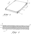
- a multiple layer foil which includes the resistive layer such as the multiple layer foil 14 shown in Figures 1 and 2 may be bonded to an adhesive coated polyester film.
- a lamination temperature of 300°F, (149°C) pressures ranging from 40 to 300 psi (275.8-2068.2kPa) and press times ranging from 10 to 90 seconds, laminates having peel strengths greater than 9.5 pounds per inch (65.5kPa) may be produced using a polyester film insulative layer.
- the invention has application irrespective of the manner in which the resistive layer and the conductive layer are attached to one another.
- the resistive layer is electrodeposited directly onto a matte surface of the conductive layer.
- the invention provides a novel printed circuit board material in the form of layered stock comprising at least one layer of an electrically resistive material adhered to and in intimate contact with a layer of a highly conductive material.
- a multiple layer laminate such as the laminate 10 of Figures 1 and 2 having a resistive layer 16, may be used to prepare a printed circuit board.
- a conductive line defining photoresist may be applied to the upper surface of the conductive layer 18 of the laminate 10.
- the photoresist may then be exposed in a conventional manner to a selected pattern of ultraviolet light, which is generally provided by a photographic negative containing the negative image of the combined resistor and conductor pattern.
- the photoresist is then developed by removal of unexposed areas of the resist film.
- a patterned photoresist layer i.e., a conductive line mask
- the term "mask” is defined in this application as the cured (i.e., patterned) photoresist layer.
- the masked laminate 10 is then treated so as to expose the multiple foil layer 14 to a preferential etchant capable of preferentially etching the conductor layer relative to the resistive layer.
- etchants may include an alkaline ammoniacal etchant, ferric or cupric chloride (acidified with hydrochloric acid), hydrogen peroxide, chromic acid or other suitable etchant, such as when the foil layer comprises a major amount of copper. Except for ammoniacal etchants and chromic acid etchants, the same types of etchants may also be used to preferentially etch foil comprising a major amount of nickel.
- Etchants such as cupric chloride (CuCl 2 )/hydrochloric acid (HCl) etchant, are often used.
- the etch bath may contain, for example, 200 grams per liter of cupric chloride and 127 ml per liter of concentrated hydrochloric acid.
- the etch bath may be maintained at a temperature of about 52°C.
- the etchant etches the copper foil 18 in those areas which are not covered by the conductive line mask.
- the exposed underlying resistive layer may be removed by contacting the exposed portions of the resistive layer of laminate 10 with a second etchant capable of etching the resistive layer.
- a second etchant capable of etching the resistive layer.
- an 18% (by weight) hydrochloric acid solution at a temperature of about 50°C or greater may be used as the resistive layer etchant.
- the laminate 10 is immersed in the hydrochloric acid solution for about 10 seconds to complete removal of the chromium-containing resistive layer 16.
- the remaining cured photoresist i.e., the conductive line masking photoresist
- a pattern of conductive lines 30, as may best be seen in Figure 3, is left behind.
- Each of the conductive lines 30 has an outer layer of conductive foil 18 and an underlying layer 16 of resistive chromium affixed to the substrate 12.
- a resistive line defining layer of a photoresist may be applied to the pattern of conductive lines illustrated in Figure 3.
- a photoresist pattern may be defined by exposing the photoresist to a pattern of ultraviolet light, such as exposing the photoresist through a photographic negative, and the unexposed portions of photoresist removed (generally by washing it away), all in a conventional manner. Portions of the resistive line photoresist (i.e., the developed image) remain behind to mask the conductive lines 30 or portions thereof which are to remain on the substrate 12.
- the foil layer 18 may then be removed at portions thereof which are not covered by the resistive line mask by immersing the laminate 10 in, or contacting the foil 18 with the etchants described above for removing foil. At this point, the conductive and resistive areas are defined and are each in appropriate contact, one with the other, to obtain a printed circuit board having a planar resistor.
- the printed circuit board may include means for electrically coupling an electrical potential to the resistive line.
- the electrically coupling means may, for example, comprise a pair of spaced copper pads adhered to the resistive line.
- the resistive line and the spaced copper pads may be created by etching respective electrodeposited layers.
- the resistive line mask described above may be removed to obtain the printed circuit board illustrated in Figure 4, which consists of a resistive line 40 comprised of a portion of the original resistive layer 16, such as a chromium-containing resistive layer, together with means for electrically coupling an electrical potential to the resistive line 40 comprising a pair of conductive copper foil end contact pads 42 and 44 which are in intimate electrical contact with the resistive line 40.
- the pads 42 and 44 provide means for coupling the resistive line 40 to an electrical potential.
- Respective pluralities of resistive line planar resistors may be arranged in networks and interconnected by appropriate conductors to provide a variety of resistances and resistance characteristics.
- the printed circuit board of Figure 4 may also have one or more conductive foil lines 30 remaining thereon to conduct electricity in a conventional manner.
- the sheet resistances of resistive layers or lines may be deliberately altered by changing the amount of non-conductive additive electrodeposited therewith by varying the electroplating conditions or the chemistry of the plating bath.
- the multiple layer foil produced by electrodepositing a nickel-containing resistive layer on a copper conductive layer may be utilized to prepare a laminate for subsequent use in preparing a printed circuit board.
- the layer 16 is, according to the above example, a nickel-containing layer rather than the chromium-containing layer described above.
- the laminate 10 may be essentially the same as has been described above.
- the laminate 10 is made up of a multiple layer foil 14 which comprises an electrodeposited resistive nickel layer 16 bonded or laminated to the substrate 12 and a conductive copper foil layer 18 suitable for preparing printed circuits.
- the conductive foil 18 is stabilized so as to improve its resistance to oxidation.
- the laminate 10 may be produced by applying temperature and pressure as set forth above.
- the resultant laminate may be subjected to etching to prepare a printed circuit board.
- a photoresist may be applied as described above and exposed to a selected pattern of ultraviolet light. What remains after suitable development is a patterned photoresist layer or conductive line mask which covers portions of the conductive copper foil layer 18 and leaves other portions uncovered.
- the multiple foil layer 14 of the laminate 10 may then be exposed to an etchant capable of etching both the copper foil and nickel-containing resistive layer such as a ferric or cupric chloride acidified with hydrochloric acid and hydrogen peroxide.
- the cupric chloride/hydrochloric acid etchant described above is often preferred.
- the etch bath may, for example, contain 200 grams per liter of cupric chloride and 127 ml per liter of concentrated hydrochloric acid.
- the etch bath may preferably be maintained at a temperature of about 52°C.
- the resistive layer is a nickel ⁇ sulfur layer
- such an etch bath removes the copper foil 18 and the nickel ⁇ sulfur layer 16 at those areas which are not covered by the photoresist mask.
- an unidentified residue may remain on the substrate 12.
- This residue may be removed by contacting the laminate having the mask thereon with a second etchant comprising chromic acid and sulfuric acid to remove the residue from all unmasked portions of the insulative layer.
- the residue may be removed by using a residue stripping etchant made up of 300 grams per liter of chromic acid and 30 ml per liter of concentrated sulfuric acid. This bath may be maintained at a temperature of 45°C and the stripping is generally achieved in about 15 seconds.
- the remaining photoresist is then removed from the copper foil 18 and a pattern of conductive lines 30 as illustrated in Figure 3 remains.
- Each of the conductive lines 30 has an outer layer of the conductive copper foil 18 and an underlying layer of the resistive nickel layer 16 affixed to the substrate 12.
- a resistive line defining layer of a photopolymer film resist may be applied to the multiple layer printed laminate or circuit board 10.
- a second photoresist pattern may be defined by exposing the photoresist to an ultraviolet light pattern and the photoresist may then be suitably developed. Undeveloped portions of the resistive line photoresist are removed and the remaining portions present a resistive line mask covering the conductive lines 30 or portions thereof which are to remain on the substrate 12. Other portions of the conductive lines 30 are not covered by the resistive line mask.
- the exposed portions of the copper foil layer 18 of the lines 30 may then be removed by contacting the copper layer 18 with a preferential etchant such as one comprised of an aqueous solution containing 300 grams per liter of chromic acid and 30 ml per liter of concentrated sulfuric acid or an ammoniacal etchant.
- a preferential etchant such as one comprised of an aqueous solution containing 300 grams per liter of chromic acid and 30 ml per liter of concentrated sulfuric acid or an ammoniacal etchant.
- a preferential etchant such as one comprised of an aqueous solution containing 300 grams per liter of chromic acid and 30 ml per liter of concentrated sulfuric acid or an ammoniacal etchant.
- the chromic acid/sulfuric acid or ammoniacal preferential etchant generally will not attack the resistive nickel-containing layer 16.
- a printed circuit board which has a resistive line 40 comprised of the nickel-containing composite and means for electrically coupling a potential to the nickel-containing resistive line 40 comprising a pair of conductive copper foil end contact pads 42 and 44 which are in intimate electrical connection with the resistive line, as can best be seen in Figure 4.
- the printed circuit board may also have one or more of the conductive foil lines 30 remaining thereon to conduct electricity in a conventional fashion and/or a plurality of resistive lines 40 arranged in an appropriate network.
- a printed circuit board material (or PCB precursor) consists of an insulating support and outer layers of a highly conductive material on one or both of the exterior surfaces of the support.
- the method of converting the precursor material into a desired product involves the selective removal of unwanted portions of the conductive layers to leave behind conductive areas of a desired configuration.
- the invention described herein pertains to the provision of an electrically resistive material (planar resistor) to be utilized in conjunction with a highly conductive layer.
- the highly conductive layer with the electrical resistance material physically adhered thereto may then be used for the production of printed circuit boards which include resistors as well as conductors.
- the methods for the selective removal of unwanted areas from the highly conductive layer with the electrical resistance material physically adhered thereto are essentially the same as the methods that have been utilized for removing unwanted areas of conductive layers which are not joined to a resistive layer.
- the resistive layers of the invention are electrodeposited layers of a composite of a normally conductive metal component and a resistance increasing amount of a non-metallic additive as previously mentioned.
- the non-metallic additive comes from a source which initially is an ingredient of the plating bath.
- the bath includes a source of the normally conductive metal component of the resistive layer and a source of a non-metallic resistance increasing additive.
- the source of the non-metallic additive generally will be a compound that is soluble in the aqueous medium of the bath and which is not decomposed by the other ingredients of the bath.
- the source should generally be subject to decomposition upon application of the electroplating current to the plating bath. Upon decomposition of the source, the carbon, nitrogen and/or phosphorus species are released from the source and incorporated into the electrodeposited mass.
- organic acids and ionizable salts thereof are useful as sources of carbon and oxygen for the purposes of the present invention.
- acids such as formic acid, acetic acid and propionic acid and the alkali metal salts thereof have been found to be effective.
- a preferred source for carbon is propionic acid.
- Nitrogen-containing compounds such as thiourea, urea, amino acids, water-soluble proteins (such as gelatin), quaternary amines (such as tetralkylammonium salts), nitric acid, etc., and ionizable salts thereof, may be used as sources of nitrogen and oxygen for the present invention.
- Water soluble or dispersable organic compounds having nitrogen-containing groups, such as amine, nitrate and nitrile groups, may be used as sources of nitrogen and carbon.
- Phosphorus-containing compounds such as ortho- and pyrophosphoric acids; meta-, ortho- and pyrophosphorous acids; and numerous organophosphosphorous compounds, such as aminotrimethylene phosphonic acid (ATMP), etc.; and ionizable salts thereof, may be used as sources of phosphorus.
- organophosphosphorous compounds such as aminotrimethylene phosphonic acid (ATMP), etc.; and ionizable salts thereof, may be used as sources of phosphorus.
- Various combinations of elements can be provided either by admixing the respective sources mentioned above or by using, as a source, a compound which has the desired elements as part of its composition.
- Bath soluble or dispersable organic compounds with amine nitrate, phosphate and/or carboxylic acid groups may also be used as a source of nitrogen, phosphorus and carbon atoms, respectively.
- a bath soluble or dispersable organic compound having one or more carboxylic groups and one or more nitrogen-containing groups may be used as a source of carbon and nitrogen, for example.
- the source of the normally conductive metal is generally the same as that which would be used for conventional plating baths known in the art.
- the source of chromium may be chromium trioxide and trivalent chrome stabilized in solution by one or more complexing agents known in the art, etc.
- the complexing agents may include, for example, aspartic acid, amino diacetic acid, nitrilo triacetic acid, 5-sulfosalicylic acid, citric acid, or a mixture of formate and glycine (1:1 molar ratio).
- Trivalent chromium-containing baths are described in detail in U.S. Patent No. 4,448, 648.
- the source of cobalt may be an ionizable salt of cobalt, such as cobalt sulfate, cobalt acetate, etc.
- the source of vanadium may be an ionizable salt of vanadium such as vanadyl sulfate trihydrate or sodium metavanadate or, preferably, an oxide such as vanadium pentoxide, etc.
- the source of tungsten may be an ionizable salt of tungsten such as sodium tungstate, or preferably, tungstic acid, etc.
- the source of molybdenum may be an ionizable salt of molybdenum such as sodium molybdate or, preferably, molybdic acid, etc.
- Suitable sources generally are acids and ionizable salts of the respective metals.
- the anion of the ionizable salts is generally one of the anions already present in the bath as a catalyst or as a source for a non-conductive additive.
- the above metals may be combined in single bath formulations to obtain properties not obtainable with any of the above metals taken individually. Examples include combining a source of chromium with a source of one or more of cobalt, vanadium, titanium, etc., (see conductive metals described above) and combining any of these conductive metal sources with a source of molybdenum or tungsten.
- One of the preferred resistive materials of the invention comprises a composite containing chromium combined with tungsten and/or molybdenum as the normally conductive metal component, and carbon and oxygen as the non-metallic additive.
- a resistive layer containing a preferred atom ratio of molybdenum or tungsten to other metals can be obtained, for example, by incorporating about 100 grams per liter molybdic acid or about 200 grams per liter tungstic acid into a plating bath prepared according to the present invention.
- the non-metallic additive is distributed throughout the composite.
- the distribution of the non-metallic additive is substantially uniform throughout the bulk of the resistive layer.
- X-ray diffraction patterns obtained for the chromium ⁇ carbon ⁇ oxygen resistive layer show that the composite comprises a minor phase of a simple cubic crystal lattice structure, and a major phase of a body centered cubic (bcc) crystal lattice structure, whereas the simple cubic phase is not detectable in the X-ray diffraction pattern of chromium electrodeposited without the non-metallic additive.
- the resistance of the resistive layer is related to the concentration of the non-metallic additive in the composite. To achieve resistance (or resistivity) in a range preferred for use in printed circuit boards and similar applications.
- the average ratio of the total number of carbon, nitrogen, and phosphorus atoms to the total number of normally conductive metal atoms is at least about 0.001:1 in the bulk of the resistive layer.
- a preferred concentration of normally conductive metal in the bulk of the resistive composite is at least about 80 weight percent. It is especially preferred that the resistive layer contain at least about 80 weight percent chromium.
- the resistive layer contains at least about 0.02 weight percent carbon, nitrogen and/or phosphorus.
- the bulk of the resistive layer is that portion of the resistive layer in which the composition is substantially uniform (i.e., that portion which is substantially unaffected by surface contamination). That portion generally begins less than approximately 50 angstroms below the surface of the resistive foil when the resistive foil is on the matte side of a low profile copper foil and generally less than about 20 below the surface angstroms when plated on a smooth conductive surface.
- One technique for measuring the concentration of the metallic and non-metallic atoms in the bulk resistive composite is to electrodeposit a sufficient quantity of resistor layer on a conductive surface to permit chemical analysis by conventional analytical techniques.
- One approach is to prepare a sample of the resistive layer produced by electrodeposition for a period of time substantially longer than the time required to produce the resistive layer to be used for electronic applications, so that the effect of surface contamination is reduced to a fraction of the total concentration. Preferably, that fraction is less than the typical margin of error in chemical composition analysis.
- Another approach to obtaining sufficient quantity of sample is to electrodeposit the resistive layer onto a large surface area of conductive material.
- the conductive material is dissolved from the resistive layer, such as by immersing the deposited resistive layer into a solution which is capable of dissolving the conductive material and not the resistive layer.
- a solution which is capable of dissolving the conductive material and not the resistive layer.
- the conductive material is a copper foil
- an example of such a solution is the copper etchant described below in connection with preferential etching of copper in the preparation of printed circuit boards.
- the remaining resistive layer may be analyzed by atomic absorption spectroscopy to determine metal content and another sample of the same material may undergo destructive testing to analyze for the non-metal additives.
- Carbon and nitrogen concentrations for example, may be determined by conventional techniques which involve combustion of a sample of the aforementioned resistive layer followed by infrared detection of the combustion products.
- Phosphorus content may be determined by standard wet chemistry techniques.
- the atom ratios may be calculated from the weight percent determination obtained for each element.
- the electroplating bath for preparing a resistive layer from such a material contains from about 25 to about 450 grams, preferably from about 100 to about 360 grams, and more preferably from about 200 to about 360 grams, per liter of a chromium source, such as chromic acid anhydride, from about 0.1 to about 2.35 grams per liter of sulfuric acid, from 0 to about 50 grams per liter of an oxy-halo acid anion and from about 20 to about 300 grams per liter of an organic, preferably aliphatic, acid.
- a chromium source such as chromic acid anhydride
- sulfuric acid from 0 to about 50 grams per liter of an oxy-halo acid anion
- organic, preferably aliphatic, acid preferably aliphatic, acid.
- the quantity of the organic acid needs to be sufficient to achieve the objective of the invention which is to provide a sufficient amount of carbon additive in the resistive layer to produce the desired resistivity.
- Resistivity varies with the amount of the additive (as discussed above). Thus, resistivity is generally reduced when the amount of the additive incorporated into the electrodeposited resistive layer is decreased.
- the amount of the additive in the electrodeposited resistive layer varies with the amount of the source thereof which is originally dissolved in the bath. For example, the sheet resistance of the deposited resistive layer comprising carbon will vary with the amount of the organic acid in the electroplating bath (other conditions being equal). Due to the nature of the electroplating operation, the variance is not always direct and the exact relationship between the amount of the source acid in the bath and the resistivity of the electroplated resistive layer is generally determined empirically.
- the temperature of the plating bath may generally be maintained in the range of from about 5 to about 50°C during the electroplating operation.
- the current density is generally in the range from about 50 amperes per square foot up to the maximum density obtainable with the equipment at hand. In this regard, the maximum current density is limited only by criteria which are well known to those of ordinary skill in the electroplating art.
- the plating bath provided by the invention may include a substance which in this invention acts as a catalyst.
- the catalyst may comprise oxy-halo anions such as periodate, iodate, perbromate, bromate, perchlorate or chlorate ions.
- the catalyst may also include sulfate ions. The presence of a catalyst is preferred for mass production of resistive layers having uniform and predictable sheet resistance or resistivity.
- Oxy-halo acid anions are the primary catalyst which may be used in the electroplating bath to promote deposition of chromium.
- a synergistic effect is seen when oxy-halo ions are used in combination with sulfuric acid.
- Chlorate, bromate and iodate ions have been found to be effective and in this regard the iodate is more effective than the bromate, which, in turn is more effective than the chlorate.
- Peroxy-halo ions such as periodate, perbromate and perchlorate are also effective for the purposes of the invention.
- the oxy-halo acid anion may be provided by using the sodium or potassium salt of chloric acid, that is either sodium or potassium chlorate, the main reason being the relative low cost and ease of availability of these materials.
- oxy-halo acid anions are powerful oxidizers and similar catalytic effects have been noted with other powerful oxidizers, for example, the permanganate ion.
- the latter anion is not completely satisfactory, however, in that it tends to be source of manganese which ends up in the electrodeposited layer and changes its character.
- Sulfuric acid may be used as a source of sulfate anion, a known catalyst for the deposition of many normally conductive metals including those used in making the resistive layer of the present invention.
- the deposition of chrome, for example, is catalyzed by this anion.
- the source of non-conductive additive in the electroplating bath provides non-conductive additive for the resultant resistive layer.
- An organic acid for example, releases oxygen and carbon atoms from the acid upon decomposition as a result of the application of current, which end up in the lattice of the deposited layer to thereby decrease the conductivity (i.e., increase the resistivity) thereof.
- the impurities and defects in the crystal lattice of the resistive material may have the effect of decreasing the conductivity relative to that of the pure bulk material.
- the resistive layer has an intrinsically lower conductivity (or higher sheet resistance) than the metal component itself would have.
- the resistive composite materials of the invention contain two components, (i,e., the metallic component and the non-metallic additive) and the resultant electrodeposited composite may be in the form of a solid solution, pure elements, interelemental compounds and/or mixtures thereof.
- the resistive layers produced in accordance with the invention need only be of sufficient thickness to be dimensionally stable during storage and further processing and utilization as a printed circuit board component.
- the resistive layers of the invention have thicknesses in the range of from about 0.1 to about 0.4 microns ( ⁇ ).
- electrodeposited layers and the like have rough surfaces such that specific numbers for thickness are actually average thicknesses.
- An objective is to provide a material which preferably has a bulk resistivity greater than about 600 ⁇ cm and which is electrodeposited in a layer having a thickness of about 0.1 to about 0.4 ⁇ so as to provide sheet resistances in the range of from about 15 to about 1000 ⁇ per square, such as about 25 ⁇ per square.
- the material produced in accordance with the invention may be referred to as a composite of the metallic and the non-metallic components and the same is not necessarily an alloy or a dispersion. However, the latter phases or states are possibly achieved. Because of the dimensional and physical characteristics of the resistive layer, it is somewhat difficult to determine the exact chemistry thereof or even the exact ratio of the ingredients therein. Accordingly, the desired resistivity characteristics are generally obtained empirically by varying the amounts of the components in the electroplating bath and measuring the resistance of the resultant electrodeposited layer until the desired resistance is achieved.
- Optimum current densities generally fall in the range from about 75 to about 300 amperes per square foot (ASF) (807-3229 amperes/m 2 ) and differ from one bath formulation to another.
- Plating time is directly related to the thickness of the deposit. Longer plating times generally produce thicker deposits and therefore lower sheet resistances, while shorter plating times generally provide higher sheet resistances.
- the agitation of the bath during the electrodeposition process enhances mass transfer to raise the limits of operable currents and improve deposition efficiency.
- the electrodeposited resistive layer be as uniform as possible.
- deposition efficiency and uniformity are sensitive to electrode configuration.
- Horizontal cells work well while the conventional vertical cells tend to yield poor uniformity.
- electrode gap With regard to electrode gap, larger gaps lead to higher solution resistance, resulting in higher electric power consumption, but contribute to better current distribution and therefore better deposit uniformity.
- a 2 inch (0.05m) gap In a 5 inch by 5 inch (0.13m) horizontal cell used in accordance with the present invention, a 2 inch (0.05m) gap has been extensively tested with good results.
- Uniformity of the electrodeposited resistive layer is related to the roughness of the substrate upon which the deposit is made. In order to achieve good uniformity, substrates with a lesser degree of roughness are more desirable. The use of substrates with a lesser degree of roughness, however, may result in a double layer foil which has an insufficient peel strength. Thus, a compromise between uniformity and peel strength is necessary in the selection of the substrate.
- the chromium resistive material may be produced from a bath which contains only an organic acid, a chromium source such as chromic anhydride and sulfate ions.
- the chromium resistive material may also be produced from baths which contain only oxy-halo anions, a chromium source such as chromic anhydride and sulfuric acid, or baths containing only oxy-halo anions, a chromium source such as chromic anhydride and the organic acid.
- oxy-halo anions allows the bath to be more tolerant of increased sulfate levels.
- the sheet resistance of a resistor layer varies with the concentration of the normally conductive metal source, such as chromic acid anhydride, and catalysts, such as the sulfuric acid in the bath. Sheet resistance also varies with solution temperature and current density during the electroplating operation.
- the sheet resistance of the electroplated layer is most sensitive to sulfuric acid concentration. Increasing the amount of sulfuric acid causes sheet resistance to decrease initially and to then increase after passing a region of minimum resistance, as shown in Table 3.
- Table 3 Also shown in Table 3 are the accompanying changes in the total quantity of chromium deposited per square decimeter of chromium resistive layer. This data indicates that decreases in sheet resistance are accompanied by increases in milligrams of Cr per square decimeter of resistive layer (mg/dm 2 ), and vice versa. The mg/dm 2 is generally highest in the layer having the lowest resistance, thus providing an indication of the point where deposition efficiency is higher. From Table 3 it can therefore be seen that the highest deposition efficiency occurs at the point where the sulfuric acid concentration is in the range from about 200 to about 250 ppm.
- the sheet resistance of the electrodeposited resistive layer is not as sensitive to variation of the concentrations of the other ingredients.
- the effects of varying the concentrations of these ingredients are similar to the sulfuric acid effects in that a condition may be identified where sheet resistance is at its minimal level, and this occurs at about 275 grams per liter for the chromic acid and between about 140 and 170 grams per liter for the acetic acid.
- Table 4 set forth below illustrates the fact that the preferred solution temperature range is from about 28 to about 33°C. Sheet resistances tend to be higher at temperatures below and above the preferred range. This Table indicates that temperatures in the range of from about 28 to 48°C can be employed to produce a desired sheet resistance simply by adjusting the plating times.
- Table 5 illustrates that the sheet resistance of the deposited resistive layer is significantly lower with a current density of 300 amperes per square foot (27-87 amperes/m 2 ) than with a current density of 600 amperes per square foot (55.74 amperes/m 2 ).
- the deposition of chromium is promoted when sodium chlorate is added to a resistive chrome electroplating bath such as one containing 300 grams per liter CrO 3 , 200 grams per liter acetic acid and 100 ppm sulfuric acid.
- a resistive chrome electroplating bath such as one containing 300 grams per liter CrO 3 , 200 grams per liter acetic acid and 100 ppm sulfuric acid.
- the presence of sodium chlorate in the bath results in lower sheet resistances as shown in Table 6.
- the current density was 300 amps/sq ft. (3229 amperes/m 2 )
- the bath temperature was 30°C
- the plating time was 45 seconds in each case. It is believed that the presence of the chlorate simply results in an increase in the deposition rate of the chromium.
- chlorates and other oxyhalides are used in the plating bath, the electroplating operation is more efficient and more easily controlled.
- Acetic acid is used as the organic acid in the experiments used to develop the data for the foregoing tables.
- propionic acid may be one of the best presently known materials for use as a source of carbon and oxygen in the chromium resistive layer.
- a bath was prepared to contain 300 grams per liter CrO 3 , 15 ml per liter of propionic acid, and 3 grams per liter of sodium chlorate.
- the plating conditions were a bath temperature of 22°C, a current density of 75 amps per square foot (807 amps/m 2 ), and a plating time of 45 seconds.
- the resistive layer thus produced had a sheet resistance of 25 ⁇ per square.
- bath chemistries and modes of operation of certain plating bath formulations are set forth in the following Table 7.
- the plating operations were conducted in a horizontal beaker cell and in each case a sheet resistance of 25 ⁇ per square was achieved.
- the copper substrate is used as the cathode in the process and the resistive chromium layer is electrodeposited directly onto the matte side of the plain and stabilized copper foil.
- Formulation III is preferred primarily because this formulation enables one to achieve high current efficiency and greater deposit uniformity.
- the result of each plating operation is a multiple layer foil that comprises an electrodeposited resistive chromium layer having a thickness of about 0.25 to about 0.35 ⁇ and a conductive copper layer having a thickness of about 35 ⁇ .
- the resistive layer produced by electroplating Formulation I has a chromium content of about 90 weight percent, a carbon content of about 0.64 weight percent and an oxygen content of about 2.83 weight percent, so that the atom ratio of carbon to chromium is about 0.031:1 and the atom ratio of oxygen to chromium is about 0.10:1.
- the resistive layer produced by electroplating Formulation III also has a chromium content of about 90 weight percent, but has a carbon content of 0.063 weight percent and an oxygen content of about 0.39 weight percent, so that the atom ratio of carbon to chromium is about 0.003 and the atom ratio of oxygen to chromium is about 0.014:1.
- each resistive layer prepared according to Table 7 is within the preferred 15 to 1,000 ⁇ per square range and the resistivity of each is greater than about 600 ⁇ per cm.
- a multiple layer foil produced using plating bath Formulation III chemistry and operating conditions as set forth in Table 7 was bonded, with the copper conductive layer facing out, to a prepreg consisting of plurality of woven glass layers coated initially with a partially cured epoxy liquid resin.
- prepregs are well known to those skilled in the art and are readily available commercially.
- the bonding operation consists of the application of heat and pressure to the structure and the result is a laminate 10 as illustrated in Figures 1 and 2, where the multiple layer foil is identified by the reference numeral 14, the copper conductive foil layer is identified by the reference numeral 18, the resistive chromium layer is identified by the reference numeral 16 and an insulative layer produced by the application of heat and pressure to the prepreg is identified by the reference numeral 12.
- the thicknesses of the various layers shown in the drawings are not necessarily to scale.
- the resistive layers produced in accordance with the invention described herein have excellent thermal and aging stability.
- the chromium resistive layers for example, generally have a temperature coefficient of resistance below about 300 ppm/°C in the 20°C to 100°C temperature range. That is to say, for sheet resistances of about 25 ⁇ per square, for example, the sheet resistance in the stated temperature range will increase about .0075 ⁇ per square for each degree Celsius of temperature increase.
- Chromium-containing resistive layers such as chromium ⁇ carbon ⁇ oxygen resistive layers, also are resistant to corrosion, a property which contributes greatly to product stability during storage, further processing operations and field applications.
- a resistive material comprising an electrodeposited layer of a composite of chromium and a resistance increasing amount of a non-metallic additive such as carbon, nitrogen and/or phosphorus.
- Chromium-containing resistive materials such as chromium ⁇ carbon ⁇ oxygen resistive materials
- resist etching by copper etchants such as a cupric chloride/hydrochloric acid etchant, and such etchant may therefore be utilized to selectively remove copper. This facilitates the control of the etching procedure which results in an increase in the quality of the end product.
- resistive chromium layers may be etched using a chromic acid etchant, the etching steps do not require the use of chromic acid as a reagent. This reduces environmental problems associated with disposal of chromic acid and chromic acid contaminated materials.
- the chromium resistive materials of the invention are also unetchable by H 2 O 2 /H 2 SO 4 , FeCl 3 , alkaline ammoniacal and CUCl 2 etchants (which do remove copper) whereby an etchant may be selected to provide an appropriate differential etch rate depending upon the etch characteristics of the particular conductive and resistive layers employed.
- This ability to conduct differential etching according to this invention may be conducted with other resistive and conductive layers when the appropriate etchants are selected.
- the intrinsically greater sheet resistance of the resistive layers of the present invention allows the layer to be applied over the entire surface of the conductor, without the necessity for using mechanical or chemical means for thinning or removing the layers in selected areas to thereby decrease the effective cross-sectional area of the layers to achieve the desired sheet resistance at localized positions.
- the desired sheet resistance may be achieved by varying the chemical content of the electroplating bath and/or the electroplating conditions.
- the resistive layers of the invention are utilized in such a manner as to entirely cover the conductor surface. Moreover, after the resistive layer has been laminated to a dielectric substrate and the conductor removed in the desired areas, the resistive layer completely covers the dielectric substrate. When the resistor has been defined correctly by using proper masking design and art work, post-processing of the resistive material by mechanical and/or chemical means is not required to achieve the desired resistance.
- the thickness of above-mentioned layer 16, for example, may be varied to achieve the commercially required dimensions of the planar resistor and sheet resistance thereof.
- the thickness of the conductive layer 18 does not effect the resistance of the resistor.
- a layer 16 produced in accordance with the invention to achieve a sheet resistance of 25 ⁇ /square will have a thickness in the range of from about 0.1 to about 0.4 ⁇ .
- the targeted sheet resistance range may be from about 15 to about 1000 ⁇ per square.
- Functional resistors can be made with any sheet resistance in this range by controlling the geometry of the etched resistor, i.e., by varying the length and the width of the etched resistor on the circuit board. Inside this resistance range, a sheet resistance value of about 25 ⁇ per square is often preferred for simplification of production processes.
- plating bath conditions such as concentration of bath ingredients and temperatures, may be employed to produce resistors having a predetermined sheet resistance, such as about 25 ⁇ per square.
- sheet resistances of 25, 100 and 1000 ⁇ /square can be achieved in accordance with the present invention and conveniently employed to make planar resistors having resistances in the commercially desirable range of from 1 ⁇ to 1 Mega ⁇ .
- the resistors of the invention may be mass produced within narrow error tolerance specifications. Reproduceability within ⁇ 2.5 percent or less of the targeted resistivity may be achieved.
Landscapes
- Engineering & Computer Science (AREA)
- Microelectronics & Electronic Packaging (AREA)
- Manufacturing & Machinery (AREA)
- Physics & Mathematics (AREA)
- Electromagnetism (AREA)
- Parts Printed On Printed Circuit Boards (AREA)
- Laminated Bodies (AREA)
- Apparatuses And Processes For Manufacturing Resistors (AREA)
- Non-Adjustable Resistors (AREA)
- ing And Chemical Polishing (AREA)
- Manufacturing Of Printed Wiring (AREA)
- Superconductors And Manufacturing Methods Therefor (AREA)
- Production Of Multi-Layered Print Wiring Board (AREA)
- Chemically Coating (AREA)
Applications Claiming Priority (2)
| Application Number | Priority Date | Filing Date | Title |
|---|---|---|---|
| US07/750,070 US5243320A (en) | 1988-02-26 | 1991-08-26 | Resistive metal layers and method for making same |
| US750070 | 1991-08-26 |
Publications (2)
| Publication Number | Publication Date |
|---|---|
| EP0530003A1 EP0530003A1 (en) | 1993-03-03 |
| EP0530003B1 true EP0530003B1 (en) | 1999-03-31 |
Family
ID=25016363
Family Applications (1)
| Application Number | Title | Priority Date | Filing Date |
|---|---|---|---|
| EP92307753A Expired - Lifetime EP0530003B1 (en) | 1991-08-26 | 1992-08-26 | Resistive metal layers and method for making same |
Country Status (12)
| Country | Link |
|---|---|
| US (1) | US5243320A (zh) |
| EP (1) | EP0530003B1 (zh) |
| JP (1) | JPH05205904A (zh) |
| KR (1) | KR930005516A (zh) |
| CN (1) | CN1032721C (zh) |
| AT (1) | ATE178450T1 (zh) |
| AU (1) | AU2112392A (zh) |
| BR (1) | BR9203407A (zh) |
| CA (1) | CA2076738A1 (zh) |
| DE (1) | DE69228781T2 (zh) |
| MX (1) | MX9204898A (zh) |
| TW (1) | TW199260B (zh) |
Families Citing this family (55)
| Publication number | Priority date | Publication date | Assignee | Title |
|---|---|---|---|---|
| US5431776A (en) * | 1993-09-08 | 1995-07-11 | Phibro-Tech, Inc. | Copper etchant solution additives |
| US5680092A (en) * | 1993-11-11 | 1997-10-21 | Matsushita Electric Industrial Co., Ltd. | Chip resistor and method for producing the same |
| DE59605278D1 (de) * | 1995-03-09 | 2000-06-29 | Philips Corp Intellectual Pty | Elektrisches Widerstandsbauelement mit CrSi-Widerstandsschicht |
| TW420729B (en) * | 1996-02-12 | 2001-02-01 | Gould Electronics Inc | A non-cyanide brass plating bath and a method of making metallic foil having a brass layer using the non-cyanide brass plating bath |
| US5794327A (en) * | 1996-03-05 | 1998-08-18 | Bird Electronic Corporation | Method for making copper electrical connections |
| US6117300A (en) * | 1996-05-01 | 2000-09-12 | Honeywell International Inc. | Method for forming conductive traces and printed circuits made thereby |
| US6301122B1 (en) * | 1996-06-13 | 2001-10-09 | Matsushita Electric Industrial Co., Ltd. | Radio frequency module with thermally and electrically coupled metal film on insulating substrate |
| US6210592B1 (en) * | 1998-04-29 | 2001-04-03 | Morton International, Inc. | Deposition of resistor materials directly on insulating substrates |
| US6329899B1 (en) * | 1998-04-29 | 2001-12-11 | Microcoating Technologies, Inc. | Formation of thin film resistors |
| AU5234099A (en) * | 1998-07-31 | 2000-02-21 | Oak-Mitsui Inc. | Composition and method for manufacturing integral resistors in printed circuit boards |
| TW446627B (en) * | 1998-09-30 | 2001-07-21 | Toyo Kohan Co Ltd | A clad sheet for lead frame, a lead frame using thereof and a manufacturing method thereof |
| US6081014A (en) * | 1998-11-06 | 2000-06-27 | National Semiconductor Corporation | Silicon carbide chrome thin-film resistor |
| JP4503122B2 (ja) * | 1999-10-19 | 2010-07-14 | コーア株式会社 | 電流検出用低抵抗器及びその製造方法 |
| US6489034B1 (en) | 2000-02-08 | 2002-12-03 | Gould Electronics Inc. | Method of forming chromium coated copper for printed circuit boards |
| US6489035B1 (en) | 2000-02-08 | 2002-12-03 | Gould Electronics Inc. | Applying resistive layer onto copper |
| US6547946B2 (en) * | 2000-04-10 | 2003-04-15 | The Regents Of The University Of California | Processing a printed wiring board by single bath electrodeposition |
| US6622374B1 (en) | 2000-09-22 | 2003-09-23 | Gould Electronics Inc. | Resistor component with multiple layers of resistive material |
| KR100402263B1 (ko) * | 2000-09-22 | 2003-10-17 | 고울드 일렉트로닉스 인코포레이티드 | 다층의 저항 재료를 갖는 저항 구성요소 |
| US6576489B2 (en) * | 2001-05-07 | 2003-06-10 | Applied Materials, Inc. | Methods of forming microstructure devices |
| TW518616B (en) * | 2001-06-01 | 2003-01-21 | Phoenix Prec Technology Corp | Method of manufacturing multi-layer circuit board with embedded passive device |
| DE10155259C1 (de) * | 2001-11-09 | 2003-05-22 | Ges Foerderung Spektrochemie | Miniaturisiertes Ionenbeweglichkeitsspektrometer |
| JP2004040073A (ja) * | 2002-01-11 | 2004-02-05 | Shipley Co Llc | 抵抗器構造物 |
| JP2004006612A (ja) * | 2002-04-12 | 2004-01-08 | Mitsui Mining & Smelting Co Ltd | キャリア箔付銅箔及びそのキャリア箔付銅箔の製造方法並びにそのキャリア箔付銅箔を用いた銅張積層板 |
| JP2004014888A (ja) * | 2002-06-10 | 2004-01-15 | Mitsui Mining & Smelting Co Ltd | プリント配線板の製造方法及びその製造方法で得られたプリント配線板 |
| US6897761B2 (en) * | 2002-12-04 | 2005-05-24 | Cts Corporation | Ball grid array resistor network |
| TW556452B (en) * | 2003-01-30 | 2003-10-01 | Phoenix Prec Technology Corp | Integrated storage plate with embedded passive components and method for fabricating electronic device with the plate |
| JP4217778B2 (ja) * | 2003-04-11 | 2009-02-04 | 古河電気工業株式会社 | 抵抗層付き導電性基材、抵抗層付き回路基板及び抵抗回路配線板 |
| US6824880B1 (en) | 2003-05-15 | 2004-11-30 | Ga-Tek, Inc. | Process for improving adhesion of resistive foil to laminating materials |
| US20050046543A1 (en) * | 2003-08-28 | 2005-03-03 | Hetzler Ullrich U. | Low-impedance electrical resistor and process for the manufacture of such resistor |
| KR100560717B1 (ko) * | 2004-03-11 | 2006-03-13 | 삼성전자주식회사 | 잉크젯 헤드 기판, 잉크젯 헤드 및 잉크젯 헤드 기판의제조방법 |
| US7342804B2 (en) * | 2004-08-09 | 2008-03-11 | Cts Corporation | Ball grid array resistor capacitor network |
| TWI315648B (en) * | 2004-11-17 | 2009-10-01 | Phoenix Prec Technology Corp | Circuit board structure with embeded adjustable passive components and method for fabricating the same |
| KR100846477B1 (ko) | 2005-01-21 | 2008-07-17 | 삼성에스디아이 주식회사 | 탄소-금속 복합재료 및 그의 제조방법 |
| US7589407B2 (en) * | 2005-04-11 | 2009-09-15 | Stats Chippac Ltd. | Semiconductor multipackage module including tape substrate land grid array package stacked over ball grid array package |
| US20060286696A1 (en) * | 2005-06-21 | 2006-12-21 | Peiffer Joel S | Passive electrical article |
| JP2007165816A (ja) * | 2005-11-15 | 2007-06-28 | Mitsui Mining & Smelting Co Ltd | プリント配線基板、その製造方法およびその使用方法 |
| US7456114B2 (en) * | 2005-12-21 | 2008-11-25 | Kesheng Feng | Microetching composition and method of using the same |
| US7875558B2 (en) * | 2005-12-21 | 2011-01-25 | Kesheng Feng | Microetching composition and method of using the same |
| JP4907479B2 (ja) * | 2007-09-19 | 2012-03-28 | 日本メクトロン株式会社 | 抵抗素子を内蔵したプリント配線板の製造法 |
| DE102007046907B4 (de) * | 2007-09-28 | 2015-02-26 | Heraeus Sensor Technology Gmbh | Schichtwiderstand und Verfahren zu dessen Herstellung |
| KR100965329B1 (ko) * | 2008-01-25 | 2010-06-22 | 엘에스엠트론 주식회사 | 인쇄회로기판용 저항 적층 도전체 및 그 제조방법과인쇄회로기판 |
| KR101426038B1 (ko) * | 2008-11-13 | 2014-08-01 | 주식회사 엠디에스 | 인쇄회로기판 및 그 제조방법 |
| JP5391981B2 (ja) * | 2009-02-02 | 2014-01-15 | 富士通株式会社 | 回路基板とその製造方法、及び抵抗素子 |
| SG181906A1 (en) * | 2010-01-15 | 2012-07-30 | Jx Nippon Mining & Metals Corp | Electronic circuit, method for forming same, and copper clad laminate for forming electronic circuit |
| WO2013086139A1 (en) * | 2011-12-07 | 2013-06-13 | Duke University | Synthesis of cupronickel nanowires and their application in transparent conducting films |
| CN103643085B (zh) * | 2013-11-13 | 2015-09-30 | 中国科学院深圳先进技术研究院 | 埋入式薄膜电阻材料及其制备方法 |
| JP6345818B2 (ja) * | 2017-01-20 | 2018-06-20 | エステー産業株式会社 | インクカートリッジ及びチップ |
| RU2681521C2 (ru) * | 2017-07-14 | 2019-03-07 | Акционерное общество "Омский научно-исследовательский институт приборостроения" (АО "ОНИИП") | Способ получения заданной конфигурации пленочных резисторов на основе тантала и его соединений |
| TWI641001B (zh) * | 2018-01-22 | 2018-11-11 | 國立屏東科技大學 | 薄膜電阻合金 |
| CN108323008B (zh) * | 2018-03-06 | 2020-10-02 | 深圳崇达多层线路板有限公司 | 一种埋电阻软硬结合板的制作方法 |
| US20220190483A1 (en) * | 2019-03-29 | 2022-06-16 | Nitto Denko Corporation | Impedance matching film for radio wave absorber, impedance matching film-attached film for radio wave absorber, radio wave absorber, and laminate for radio wave absorber |
| CN111198411A (zh) * | 2020-03-02 | 2020-05-26 | 苏州中为联创微纳制造创新中心有限公司 | 一种具有金属网格结构的衍射光学镜片及其制作方法 |
| JP7089555B2 (ja) * | 2020-07-03 | 2022-06-22 | 大同特殊鋼株式会社 | 電流検出用抵抗器、回路基板及び電流検出用抵抗器の製造方法 |
| CN114126239A (zh) * | 2020-08-28 | 2022-03-01 | 宏启胜精密电子(秦皇岛)有限公司 | 具有内埋薄膜电阻的线路板及其制作方法 |
| CN113571275B (zh) * | 2021-06-24 | 2022-03-11 | 贝迪斯电子有限公司 | 一种片式合金箔电阻的制造方法 |
Family Cites Families (58)
| Publication number | Priority date | Publication date | Assignee | Title |
|---|---|---|---|---|
| BE503299A (zh) * | 1949-10-29 | |||
| US2662957A (en) * | 1949-10-29 | 1953-12-15 | Eisler Paul | Electrical resistor or semiconductor |
| US2671950A (en) * | 1950-03-09 | 1954-03-16 | Sukacev Lev | Method of constructing thermopiles |
| US2643221A (en) * | 1950-11-30 | 1953-06-23 | Us Army | Electrodeposition of phosphorusnickel and phosphorus-cobalt alloys |
| US3006819A (en) * | 1955-06-13 | 1961-10-31 | Sanders Associates Inc | Method of photo-plating electrical circuits |
| US3077442A (en) * | 1960-08-19 | 1963-02-12 | Ibm | Preparation of hard magnetic coatings of nickel-phosphorus alloys |
| US3218194A (en) * | 1962-04-19 | 1965-11-16 | Gold loaded tantalum film | |
| US3287161A (en) * | 1962-10-01 | 1966-11-22 | Xerox Corp | Method for forming a thin film resistor |
| US3611246A (en) * | 1964-06-01 | 1971-10-05 | James M Booe | Chromium-carbon and chromium-nickel-carbon resistive films |
| GB1054525A (zh) * | 1965-02-03 | |||
| US3522085A (en) * | 1965-12-17 | 1970-07-28 | Sanyo Electric Co | Article and method for making resistors in printed circuit board |
| US3423260A (en) * | 1966-03-21 | 1969-01-21 | Bunker Ramo | Method of making a thin film circuit having a resistor-conductor pattern |
| US3493352A (en) * | 1966-12-01 | 1970-02-03 | Gen Electric | Magneto optical display device with layers nickel-chromium and gold |
| US3607389A (en) * | 1967-10-21 | 1971-09-21 | Elettrotecnica Chimica Italian | Metallic film resistors |
| NL144810C (zh) * | 1968-02-06 | |||
| GB1234809A (en) * | 1968-03-28 | 1971-06-09 | Lorenz Westerbarkey | A perforated pipe made from metal strip, and appartus for manufacturing same |
| US3691007A (en) * | 1969-08-14 | 1972-09-12 | Mica Corp The | Printed circuit board fabrication by electroplating a surface through a porous membrane |
| US3654101A (en) * | 1970-01-09 | 1972-04-04 | M & T Chemicals Inc | Novel chromium plating compositions and processes |
| US3663241A (en) * | 1970-05-20 | 1972-05-16 | Du Pont | Metallizing composition containing nickel powder |
| US3645783A (en) * | 1970-06-03 | 1972-02-29 | Infrared Ind Inc | Thin film planar resistor |
| US3808576A (en) * | 1971-01-15 | 1974-04-30 | Mica Corp | Circuit board with resistance layer |
| US3743583A (en) * | 1971-01-15 | 1973-07-03 | Mica Corp | Printed circuit board fabrication |
| US3706639A (en) * | 1971-02-19 | 1972-12-19 | Du Pont | Rejuvenated chromium plating medium containing chromic compound |
| US3857681A (en) * | 1971-08-03 | 1974-12-31 | Yates Industries | Copper foil treatment and products produced therefrom |
| US3781596A (en) * | 1972-07-07 | 1973-12-25 | R Galli | Semiconductor chip carriers and strips thereof |
| JPS534498B2 (zh) * | 1973-06-23 | 1978-02-17 | ||
| US3857683A (en) * | 1973-07-27 | 1974-12-31 | Mica Corp | Printed circuit board material incorporating binary alloys |
| US3878006A (en) * | 1973-10-26 | 1975-04-15 | Mica Corp | Selective etchant for nickel/phosphorus alloy |
| US3947277A (en) * | 1973-12-19 | 1976-03-30 | Universal Oil Products Company | Duplex resistor inks |
| GB1419613A (en) * | 1974-06-13 | 1975-12-31 | Lea Ronal Inc | Cyanidefree electroplating baths |
| US3981691A (en) * | 1974-07-01 | 1976-09-21 | Minnesota Mining And Manufacturing Company | Metal-clad dielectric sheeting having an improved bond between the metal and dielectric layers |
| US3958317A (en) * | 1974-09-25 | 1976-05-25 | Rockwell International Corporation | Copper surface treatment for epoxy bonding |
| DE2500730C3 (de) * | 1975-01-10 | 1980-04-24 | Bergische Metallwarenfabrik Dillenberg & Co Kg, 5601 Gruiten | Galvanisches Chrombad |
| US4204935A (en) * | 1976-02-10 | 1980-05-27 | Resista Fabrik Elektrischer Widerstande G.M.B.H. | Thin-film resistor and process for the production thereof |
| DE2724498C2 (de) * | 1977-05-31 | 1982-06-03 | Siemens AG, 1000 Berlin und 8000 München | Elektrischer Schichtwiderstand und Verfahren zu seiner Herstellung |
| US4131517A (en) * | 1977-06-03 | 1978-12-26 | Nippon Mining Co., Ltd. | Surface treating process for copper foil for use in printed circuit |
| US4208698A (en) * | 1977-10-26 | 1980-06-17 | Ilc Data Device Corporation | Novel hybrid packaging scheme for high density component circuits |
| US4190474A (en) * | 1977-12-22 | 1980-02-26 | Gould Inc. | Method of making a printed circuit board having mutually etchable copper and nickel layers |
| FR2423556A1 (fr) * | 1978-03-08 | 1979-11-16 | Yissum Res Dev Co | Procede de revetement electrolytique de chrome sur divers metaux et bains utilises dans ce but |
| DE2833919C2 (de) * | 1978-08-02 | 1982-06-09 | Siemens AG, 1000 Berlin und 8000 München | Verfahren zur Herstellung von elektrischen Schichtschaltungen auf Kunststoffolien |
| US4301439A (en) * | 1978-12-26 | 1981-11-17 | Electro Materials Corp. Of America | Film type resistor and method of producing same |
| US4411768A (en) * | 1979-12-21 | 1983-10-25 | The Lummus Company | Hydrogenation of high boiling hydrocarbons |
| US4387137A (en) * | 1980-12-01 | 1983-06-07 | The Mica Corporation | Capacitor material |
| GB2110242B (en) * | 1981-11-18 | 1985-06-12 | Ibm | Electroplating chromium |
| US4444848A (en) * | 1982-01-04 | 1984-04-24 | Western Electric Co., Inc. | Adherent metal coatings on rubber-modified epoxy resin surfaces |
| DE3321900C2 (de) * | 1982-06-16 | 1986-01-16 | Nitto Electric Industrial Co., Ltd., Ibaraki, Osaka | Substrat für eine Schaltung mit einer Widerstandsschicht und Verfahren zu dessen Herstellung |
| DE3371096D1 (en) * | 1982-12-01 | 1987-05-27 | Electrofoils Techn Ltd | Treatment of copper foil |
| US4450050A (en) * | 1983-02-03 | 1984-05-22 | M&T Chemicals Inc. | Process for bonding high efficiency chromium electrodeposits |
| GB2158100B (en) * | 1984-05-01 | 1988-02-03 | Nat Res Dev | Chromium electroplating bath |
| GB8411063D0 (en) * | 1984-05-01 | 1984-06-06 | Mccormick M | Chromium electroplating |
| US4554219A (en) * | 1984-05-30 | 1985-11-19 | Burlington Industries, Inc. | Synergistic brightener combination for amorphous nickel phosphorus electroplatings |
| JPS61236192A (ja) * | 1985-04-12 | 1986-10-21 | 株式会社日立製作所 | セラミツク基板の電極形成方法 |
| US4808967A (en) * | 1985-05-29 | 1989-02-28 | Ohmega Electronics | Circuit board material |
| JPS61288401A (ja) * | 1985-06-14 | 1986-12-18 | 株式会社村田製作所 | 薄膜抵抗体 |
| US4572768A (en) * | 1985-06-28 | 1986-02-25 | Square D Company | Treatment for copper foil |
| US4682143A (en) * | 1985-10-30 | 1987-07-21 | Advanced Micro Devices, Inc. | Thin film chromium-silicon-carbon resistor |
| JP2575109B2 (ja) * | 1985-11-08 | 1997-01-22 | ソニー株式会社 | プリント配線基板 |
| EP1011111A1 (en) * | 1988-02-26 | 2000-06-21 | Gould Electronics Inc. | Resistive metal layers and method for making same |
-
1991
- 1991-08-26 US US07/750,070 patent/US5243320A/en not_active Expired - Fee Related
-
1992
- 1992-08-19 AU AU21123/92A patent/AU2112392A/en not_active Abandoned
- 1992-08-24 CA CA002076738A patent/CA2076738A1/en not_active Abandoned
- 1992-08-25 CN CN92109686A patent/CN1032721C/zh not_active Expired - Fee Related
- 1992-08-25 MX MX9204898A patent/MX9204898A/es unknown
- 1992-08-26 AT AT92307753T patent/ATE178450T1/de not_active IP Right Cessation
- 1992-08-26 BR BR929203407A patent/BR9203407A/pt not_active Application Discontinuation
- 1992-08-26 KR KR1019920015430A patent/KR930005516A/ko not_active Application Discontinuation
- 1992-08-26 JP JP4227634A patent/JPH05205904A/ja active Pending
- 1992-08-26 DE DE69228781T patent/DE69228781T2/de not_active Expired - Fee Related
- 1992-08-26 EP EP92307753A patent/EP0530003B1/en not_active Expired - Lifetime
- 1992-09-25 TW TW081107598A patent/TW199260B/zh active
Non-Patent Citations (1)
| Title |
|---|
| "Kirk-Othmer, Encyclopedia of Chemical Technology, 3rd edition (1980), vol.12, page 432", JOHN WILEY & SONS, NEW YORK, US * |
Also Published As
| Publication number | Publication date |
|---|---|
| ATE178450T1 (de) | 1999-04-15 |
| DE69228781D1 (de) | 1999-05-06 |
| DE69228781T2 (de) | 1999-10-07 |
| CN1073547A (zh) | 1993-06-23 |
| BR9203407A (pt) | 1993-03-30 |
| CN1032721C (zh) | 1996-09-04 |
| TW199260B (zh) | 1993-02-01 |
| JPH05205904A (ja) | 1993-08-13 |
| MX9204898A (es) | 1993-04-01 |
| EP0530003A1 (en) | 1993-03-03 |
| CA2076738A1 (en) | 1993-02-27 |
| US5243320A (en) | 1993-09-07 |
| AU2112392A (en) | 1993-03-04 |
| KR930005516A (ko) | 1993-03-23 |
Similar Documents
| Publication | Publication Date | Title |
|---|---|---|
| EP0530003B1 (en) | Resistive metal layers and method for making same | |
| EP0380545B1 (en) | Improved circuit board material and electroplating bath for the production thereof | |
| US4888574A (en) | Circuit board material and method of making | |
| US4368252A (en) | Printed circuit substrate with resistance elements | |
| CN100571483C (zh) | 带载体的极薄铜箔以及使用带载体的极薄铜箔的电路板 | |
| NL8620227A (nl) | Materiaal voor een schakelbord en werkwijze voor het vervaardigen hiervan. | |
| US6660406B2 (en) | Method for manufacturing printed wiring board comprising electrodeposited copper foil with carrier and resistor circuit; and printed wiring board comprising resistor circuit | |
| US5689227A (en) | Circuit board material with barrier layer | |
| JP2001068804A (ja) | キャリア箔付電解銅箔及びその電解銅箔の製造方法並びにその電解銅箔を使用した銅張積層板 | |
| JP2000309898A (ja) | キャリア箔付電解銅箔及びその電解銅箔の製造方法並びにその電解銅箔を使用した銅張積層板 | |
| KR960001355B1 (ko) | 사전 감광 회로 물질 | |
| EP2373132A1 (en) | Method for forming electronic circuit | |
| US4220945A (en) | Printed circuit substrate with resistance coat | |
| EP0330210A2 (en) | Resistive metal layers and method for making same | |
| US6447929B1 (en) | Thin copper on usable carrier and method of forming same | |
| US20030048172A1 (en) | Composition and method for manufacturing integral resistors in printed circuit boards | |
| JP2005307270A (ja) | キャリア箔付電解銅箔及びそのキャリア箔付電解銅箔の製造方法 | |
| JP2003200523A (ja) | 抵抗層内蔵型銅張り積層板、それを用いたプリント回路基板 | |
| JP2003193291A (ja) | 抵抗層付き銅箔とその製造方法 | |
| JPH10126039A (ja) | プリント配線基板などのエッチング方法 | |
| JPS5823954B2 (ja) | テイコウタイツキカイロバンザイリヨウ | |
| DD298292A5 (de) | Galvanisierbad zur galvanischen abscheidung einer widerstandsschicht |
Legal Events
| Date | Code | Title | Description |
|---|---|---|---|
| PUAI | Public reference made under article 153(3) epc to a published international application that has entered the european phase |
Free format text: ORIGINAL CODE: 0009012 |
|
| AK | Designated contracting states |
Kind code of ref document: A1 Designated state(s): AT BE CH DE DK ES FR GB GR IE IT LI LU MC NL PT SE |
|
| 17P | Request for examination filed |
Effective date: 19930607 |
|
| RAP1 | Party data changed (applicant data changed or rights of an application transferred) |
Owner name: GOULD ELECTRONICS INC. |
|
| 17Q | First examination report despatched |
Effective date: 19941027 |
|
| GRAG | Despatch of communication of intention to grant |
Free format text: ORIGINAL CODE: EPIDOS AGRA |
|
| GRAG | Despatch of communication of intention to grant |
Free format text: ORIGINAL CODE: EPIDOS AGRA |
|
| GRAG | Despatch of communication of intention to grant |
Free format text: ORIGINAL CODE: EPIDOS AGRA |
|
| GRAH | Despatch of communication of intention to grant a patent |
Free format text: ORIGINAL CODE: EPIDOS IGRA |
|
| GRAH | Despatch of communication of intention to grant a patent |
Free format text: ORIGINAL CODE: EPIDOS IGRA |
|
| GRAA | (expected) grant |
Free format text: ORIGINAL CODE: 0009210 |
|
| AK | Designated contracting states |
Kind code of ref document: B1 Designated state(s): AT BE CH DE DK ES FR GB GR IE IT LI LU MC NL PT SE |
|
| PG25 | Lapsed in a contracting state [announced via postgrant information from national office to epo] |
Ref country code: SE Free format text: THE PATENT HAS BEEN ANNULLED BY A DECISION OF A NATIONAL AUTHORITY Effective date: 19990331 Ref country code: NL Free format text: LAPSE BECAUSE OF FAILURE TO SUBMIT A TRANSLATION OF THE DESCRIPTION OR TO PAY THE FEE WITHIN THE PRESCRIBED TIME-LIMIT Effective date: 19990331 Ref country code: LI Free format text: LAPSE BECAUSE OF FAILURE TO SUBMIT A TRANSLATION OF THE DESCRIPTION OR TO PAY THE FEE WITHIN THE PRESCRIBED TIME-LIMIT Effective date: 19990331 Ref country code: GR Free format text: LAPSE BECAUSE OF NON-PAYMENT OF DUE FEES Effective date: 19990331 Ref country code: ES Free format text: THE PATENT HAS BEEN ANNULLED BY A DECISION OF A NATIONAL AUTHORITY Effective date: 19990331 Ref country code: CH Free format text: LAPSE BECAUSE OF FAILURE TO SUBMIT A TRANSLATION OF THE DESCRIPTION OR TO PAY THE FEE WITHIN THE PRESCRIBED TIME-LIMIT Effective date: 19990331 Ref country code: BE Free format text: LAPSE BECAUSE OF FAILURE TO SUBMIT A TRANSLATION OF THE DESCRIPTION OR TO PAY THE FEE WITHIN THE PRESCRIBED TIME-LIMIT Effective date: 19990331 Ref country code: AT Free format text: LAPSE BECAUSE OF FAILURE TO SUBMIT A TRANSLATION OF THE DESCRIPTION OR TO PAY THE FEE WITHIN THE PRESCRIBED TIME-LIMIT Effective date: 19990331 |
|
| REF | Corresponds to: |
Ref document number: 178450 Country of ref document: AT Date of ref document: 19990415 Kind code of ref document: T |
|
| REG | Reference to a national code |
Ref country code: CH Ref legal event code: EP |
|
| ITF | It: translation for a ep patent filed | ||
| REG | Reference to a national code |
Ref country code: IE Ref legal event code: FG4D |
|
| REF | Corresponds to: |
Ref document number: 69228781 Country of ref document: DE Date of ref document: 19990506 |
|
| ET | Fr: translation filed | ||
| PG25 | Lapsed in a contracting state [announced via postgrant information from national office to epo] |
Ref country code: PT Free format text: LAPSE BECAUSE OF FAILURE TO SUBMIT A TRANSLATION OF THE DESCRIPTION OR TO PAY THE FEE WITHIN THE PRESCRIBED TIME-LIMIT Effective date: 19990630 Ref country code: DK Free format text: LAPSE BECAUSE OF FAILURE TO SUBMIT A TRANSLATION OF THE DESCRIPTION OR TO PAY THE FEE WITHIN THE PRESCRIBED TIME-LIMIT Effective date: 19990630 |
|
| PGFP | Annual fee paid to national office [announced via postgrant information from national office to epo] |
Ref country code: FR Payment date: 19990802 Year of fee payment: 8 Ref country code: DE Payment date: 19990802 Year of fee payment: 8 |
|
| PGFP | Annual fee paid to national office [announced via postgrant information from national office to epo] |
Ref country code: GB Payment date: 19990803 Year of fee payment: 8 |
|
| PGFP | Annual fee paid to national office [announced via postgrant information from national office to epo] |
Ref country code: MC Payment date: 19990810 Year of fee payment: 8 |
|
| PGFP | Annual fee paid to national office [announced via postgrant information from national office to epo] |
Ref country code: BE Payment date: 19990819 Year of fee payment: 8 |
|
| PGFP | Annual fee paid to national office [announced via postgrant information from national office to epo] |
Ref country code: LU Payment date: 19990820 Year of fee payment: 8 |
|
| PGFP | Annual fee paid to national office [announced via postgrant information from national office to epo] |
Ref country code: IE Payment date: 19990831 Year of fee payment: 8 |
|
| NLV1 | Nl: lapsed or annulled due to failure to fulfill the requirements of art. 29p and 29m of the patents act | ||
| REG | Reference to a national code |
Ref country code: CH Ref legal event code: PL |
|
| PLBE | No opposition filed within time limit |
Free format text: ORIGINAL CODE: 0009261 |
|
| STAA | Information on the status of an ep patent application or granted ep patent |
Free format text: STATUS: NO OPPOSITION FILED WITHIN TIME LIMIT |
|
| 26N | No opposition filed | ||
| PG25 | Lapsed in a contracting state [announced via postgrant information from national office to epo] |
Ref country code: LU Free format text: LAPSE BECAUSE OF NON-PAYMENT OF DUE FEES Effective date: 20000826 Ref country code: IE Free format text: LAPSE BECAUSE OF NON-PAYMENT OF DUE FEES Effective date: 20000826 Ref country code: GB Free format text: LAPSE BECAUSE OF NON-PAYMENT OF DUE FEES Effective date: 20000826 |
|
| PG25 | Lapsed in a contracting state [announced via postgrant information from national office to epo] |
Ref country code: MC Free format text: THE PATENT HAS BEEN ANNULLED BY A DECISION OF A NATIONAL AUTHORITY Effective date: 20000831 |
|
| GBPC | Gb: european patent ceased through non-payment of renewal fee |
Effective date: 20000826 |
|
| PG25 | Lapsed in a contracting state [announced via postgrant information from national office to epo] |
Ref country code: FR Free format text: LAPSE BECAUSE OF NON-PAYMENT OF DUE FEES Effective date: 20010430 |
|
| PG25 | Lapsed in a contracting state [announced via postgrant information from national office to epo] |
Ref country code: DE Free format text: LAPSE BECAUSE OF NON-PAYMENT OF DUE FEES Effective date: 20010501 |
|
| REG | Reference to a national code |
Ref country code: IE Ref legal event code: MM4A |
|
| REG | Reference to a national code |
Ref country code: FR Ref legal event code: ST |
|
| PG25 | Lapsed in a contracting state [announced via postgrant information from national office to epo] |
Ref country code: IT Free format text: LAPSE BECAUSE OF NON-PAYMENT OF DUE FEES;WARNING: LAPSES OF ITALIAN PATENTS WITH EFFECTIVE DATE BEFORE 2007 MAY HAVE OCCURRED AT ANY TIME BEFORE 2007. THE CORRECT EFFECTIVE DATE MAY BE DIFFERENT FROM THE ONE RECORDED. Effective date: 20050826 |