EP0509360B1 - Dynamic random access memory device with multiple word line selector used in burn-in test - Google Patents
Dynamic random access memory device with multiple word line selector used in burn-in test Download PDFInfo
- Publication number
- EP0509360B1 EP0509360B1 EP92105926A EP92105926A EP0509360B1 EP 0509360 B1 EP0509360 B1 EP 0509360B1 EP 92105926 A EP92105926 A EP 92105926A EP 92105926 A EP92105926 A EP 92105926A EP 0509360 B1 EP0509360 B1 EP 0509360B1
- Authority
- EP
- European Patent Office
- Prior art keywords
- random access
- dynamic random
- memory device
- access memory
- coupled
- Prior art date
- Legal status (The legal status is an assumption and is not a legal conclusion. Google has not performed a legal analysis and makes no representation as to the accuracy of the status listed.)
- Expired - Lifetime
Links
Images


Classifications
-
- G—PHYSICS
- G11—INFORMATION STORAGE
- G11C—STATIC STORES
- G11C11/00—Digital stores characterised by the use of particular electric or magnetic storage elements; Storage elements therefor
- G11C11/21—Digital stores characterised by the use of particular electric or magnetic storage elements; Storage elements therefor using electric elements
- G11C11/34—Digital stores characterised by the use of particular electric or magnetic storage elements; Storage elements therefor using electric elements using semiconductor devices
- G11C11/40—Digital stores characterised by the use of particular electric or magnetic storage elements; Storage elements therefor using electric elements using semiconductor devices using transistors
- G11C11/401—Digital stores characterised by the use of particular electric or magnetic storage elements; Storage elements therefor using electric elements using semiconductor devices using transistors forming cells needing refreshing or charge regeneration, i.e. dynamic cells
- G11C11/4063—Auxiliary circuits, e.g. for addressing, decoding, driving, writing, sensing or timing
- G11C11/407—Auxiliary circuits, e.g. for addressing, decoding, driving, writing, sensing or timing for memory cells of the field-effect type
-
- G—PHYSICS
- G11—INFORMATION STORAGE
- G11C—STATIC STORES
- G11C29/00—Checking stores for correct operation ; Subsequent repair; Testing stores during standby or offline operation
- G11C29/04—Detection or location of defective memory elements, e.g. cell constructio details, timing of test signals
- G11C29/50—Marginal testing, e.g. race, voltage or current testing
-
- G—PHYSICS
- G11—INFORMATION STORAGE
- G11C—STATIC STORES
- G11C29/00—Checking stores for correct operation ; Subsequent repair; Testing stores during standby or offline operation
- G11C29/04—Detection or location of defective memory elements, e.g. cell constructio details, timing of test signals
- G11C29/08—Functional testing, e.g. testing during refresh, power-on self testing [POST] or distributed testing
- G11C29/12—Built-in arrangements for testing, e.g. built-in self testing [BIST] or interconnection details
- G11C29/18—Address generation devices; Devices for accessing memories, e.g. details of addressing circuits
- G11C29/30—Accessing single arrays
- G11C29/34—Accessing multiple bits simultaneously
-
- G—PHYSICS
- G11—INFORMATION STORAGE
- G11C—STATIC STORES
- G11C11/00—Digital stores characterised by the use of particular electric or magnetic storage elements; Storage elements therefor
- G11C11/21—Digital stores characterised by the use of particular electric or magnetic storage elements; Storage elements therefor using electric elements
- G11C11/34—Digital stores characterised by the use of particular electric or magnetic storage elements; Storage elements therefor using electric elements using semiconductor devices
- G11C11/40—Digital stores characterised by the use of particular electric or magnetic storage elements; Storage elements therefor using electric elements using semiconductor devices using transistors
- G11C11/401—Digital stores characterised by the use of particular electric or magnetic storage elements; Storage elements therefor using electric elements using semiconductor devices using transistors forming cells needing refreshing or charge regeneration, i.e. dynamic cells
Definitions
- This invention relates to a dynamic random access memory device and, more particularly, to a multiple word line selector incorporated in the dynamic random access memory device for a burn-in test on the memory cells.
- the dynamic random access memory device Upon completion of fabrication process for a dynamic random access memory device, the dynamic random access memory device is subjected to various test operations, and one of the test operations is known as "burn-in test". In the burn-in test, the dynamic random access memory device is placed in high temperature ambience, and the word lines are driven to active level after writing data bits in the memory cells.
- the prior art dynamic random access memory can simultaneously drive a single or a few word lines selected from all the word lines, and the burn-in test tends to be prolonged due to the sequential drive for the word lines.
- the prior art dynamic random access memory device needs to repeat the word line drive 1024 times, and long time period is consumed for the burn-in test.
- the dynamic random access memory device is continuously increasing the memory capacity, and, accordingly, the word lines incorporated therein are increased together with the memory cells. This means that the time period tends to be prolonged, and the cost for the diagnosis is increased together with the memory capacity.
- a memory device as set out in the preamble of claim 1 and in which all word lines can be driven simultaneously is known from EP-A-0 405 576.
- the present invention proposes to simultaneously drive all of the word lines with one of the signal pins, as set out in claim 1.
- a dynamic random access memory device embodying the present invention is fabricated on a single semiconductor chip 1, and comprises a memory cell array 2 implemented by a plurality of memory cells M11, M1n, M21, M2n, Mm1 and Mmn arranged in rows and columns. Though not shown in the drawings, each of the memory cells M11 to Mmn is implemented by a series combination of an n-channel enhancement type switching transistor and a storage capacitor.
- Word lines W1, W2, W3 and Wm are respectively coupled with the memory cells M11 to Mmn in the rows of the memory cell array 2, and bit line pairs BL1 to BLn are respectively coupled with the memory cells in the columns of the memory cell array 2 for propagating data bits to associated sense amplifier circuits SA1 to SAn.
- a row address decoder and driver unit 3 is associated with the word lines W1 to Wm, and drives one of the word lines W1 to Wm indicated by row address bits.
- a column selector is coupled between the sense amplifier circuits SA1 to SAn and a data pin, and a column address decoder unit 4 allows one of the bit line pairs BL1 to BLn indicated by column address bits to couple through the column selector with the data pin.
- the dynamic random access memory device shown in Fig. 1 further comprises an auxiliary word line driver unit 5 coupled with the word lines W1 to Wm, and the auxiliary word line driver unit 5 is provided on the opposite side to the row address decoder and driver unit 3.
- the auxiliary word line driver 5 is implemented by a plurality of p-channel enhancement type switching transistors Q1, Q2, Q3 and Qm, and the drain nodes of the p-channel enhancement type switching transistors Q1 to Qm are respectively coupled with the word lines W1 to Wm.
- the source nodes of the p-channel enhancement type switching transistors Q1 to Qm are commonly coupled with a predetermined pin 6, and the predetermined pin 6 is coupled through a step-down circuit 7 with the gate electrodes of the p-channel enhancement type switching transistors Q1 to Qm.
- the step-down circuit 7 is implemented by a series combination of p-channel enhancement type load transistors Q11, Q12 and Q13, and decreases a voltage level at the predetermined pin 6.
- the dynamic random access memory device is subjected to various test operations prior to delivery from the manufacturing factory.
- the burn-in test operation is carried out for the dynamic random access memory device for screening a defective product with breakable memory cells, and the burn-in test traces the following sequence.
- data bit of logic "0" is written into all of the memory cells M11 to Mmn, and a plurality of clock pulses are supplied to the predetermined pin 6.
- Each clock pulse is distributed from the predetermined pin 6 to the source nodes of the p-channel enhancement type switching transistors Q1 to Qm, and the step-down circuit 7 supplies the gate electrodes a voltage level lower than the source nodes by the threshold level of the switching transistors Q1 to Qm.
- the p-channel enhancement type switching transistors Q1 to Qm simultaneously turn on in the presence of every clock pulse, and the clock pulses are transferred to all of the word lines W1 to Wm.
- the gate oxide films of the n-channel enhancement type switching transistors are stressed.
- data bit of logic "1" level is written into all of the memory cells M11 to Mmn, and a plurality of clock pulses are applied to a pin. The data write-in and the application of stress are repeated predetermined times, and the manufacturer diagnoses the memory cells M11 to Mmn.
- the clock pulses are simultaneously applied to all of the word lines W1 to Wm in the burn-in test operation, and the burn-in test operation is completed within short time period rather than the prior art dynamic random access memory device.
- FIG. 2 of the drawings another dynamic random access memory device embodying the present invention is fabricated on a single semiconductor chip 21.
- the dynamic random access memory device shown in Fig. 2 is similar in circuit arrangement to the first embodiment except for some additional circuits, and components are labeled with the same references as the corresponding components of the dynamic random access memory device shown in Fig. 1 without description.
- an external row address strobe signal RAS is applied to the first predetermined pin 6 in the standard mode of operation having a write-in phase and a read-out phase, and a first clock signal CLK1 is supplied to the first predetermined pin 6 in the diagnostic mode of operation.
- the first predetermined pin 6 is coupled in parallel with the auxiliary word line driving unit 5 and an internal row address strobe generator 22.
- the dynamic random access memory device implementing the second embodiment further comprises a switching circuit 23 which is implemented by a plurality of pairs of n-channel enhancement type switching transistors Q21, Q22, Q23, Q24, Q25 and Q26.
- the pairs of n-channel enhancement type switching transistors Q21 to Q26 are respectively coupled with the bit line pairs BL1, BL2 and BLn and a ground voltage line serving as a source of logic "0" level.
- the gate electrodes of the n-channel enhancement type switching transistors Q21, Q23 and Q25 are coupled with a second predetermined pin 24, and the other n-channel enhancement type switching transistors Q22, Q24 and Q26 are coupled at the gate electrodes thereof with a third predetermined pin 25.
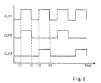
- Second and third clock signals CLK2 and CLK3 are respectively supplied to the second and third predetermined pins 24 and 25 in synchronism with the first clock signal CLK1 as shown in Fig, 3.
- the circuit behavior in the standard mode of operation is similar to that of the first embodiment, and no further description is incorporated hereinbelow for avoiding repetition.
- the dynamic random access memory device shown in Fig. 2 enters the burn-in test operation in the diagnostic mode.
- the burn-in test starts without write-in of a data bit into all of the memory cells M11, M12, M1n, M21, M22, M2n, M31, M32, M3n, Mm1, Mm2 and Mmn, and the first clock signal CLK1 is supplied to the first predetermined pin 6.
- the first clock signal CLK1 allows the auxiliary word line driving unit 5 to lift all of the word lines W1 to Wm to the active level at time t1, and the second clock signal CLK2 rises together with the first clock signal CLK1 so that the n-channel enhancement type switching transistors Q21, Q23 and Q25 discharges the associated bit lines, thereby supplying logic "0" to these bit lines.
- the first and second clock signals CLK1 and CLK2 are recovered to the low voltage level at time t2, and the first and third clock signals CLK1 and CLK3 are lifted to the high voltage level at time t3.
- the n-channel enhancement type switching transistors Q22, Q24 and Q26 turn on so as to discharge the associated bit lines, and the first and third clock signals CLK1 and CLK3 are recovered at time t4.
- the switching circuit 23 alternately supplies logic "1" level to half of the bit lines, and stress is applied to all of the memory cells M11 to Mmn without any write-in operation.
- the auxiliary word line driving unit of the dynamic random access memory device simultaneously drives all of the word lines W1 to Wm, and the burn-in test operation is completed within short time period. This results in reduction of production cost of the dynamic random access memory device.
Applications Claiming Priority (2)
| Application Number | Priority Date | Filing Date | Title |
|---|---|---|---|
| JP11556391A JP3237127B2 (ja) | 1991-04-19 | 1991-04-19 | ダイナミックランダムアクセスメモリ装置 |
| JP115563/91 | 1991-04-19 |
Publications (2)
| Publication Number | Publication Date |
|---|---|
| EP0509360A1 EP0509360A1 (en) | 1992-10-21 |
| EP0509360B1 true EP0509360B1 (en) | 1997-07-23 |
Family
ID=14665646
Family Applications (1)
| Application Number | Title | Priority Date | Filing Date |
|---|---|---|---|
| EP92105926A Expired - Lifetime EP0509360B1 (en) | 1991-04-19 | 1992-04-06 | Dynamic random access memory device with multiple word line selector used in burn-in test |
Country Status (5)
| Country | Link |
|---|---|
| US (1) | US5293340A (ja) |
| EP (1) | EP0509360B1 (ja) |
| JP (1) | JP3237127B2 (ja) |
| KR (1) | KR950014247B1 (ja) |
| DE (1) | DE69221005T2 (ja) |
Families Citing this family (20)
| Publication number | Priority date | Publication date | Assignee | Title |
|---|---|---|---|---|
| JP2793427B2 (ja) * | 1992-04-08 | 1998-09-03 | 株式会社東芝 | 半導体装置 |
| JPH0628861A (ja) * | 1992-07-07 | 1994-02-04 | Oki Electric Ind Co Ltd | 半導体記憶装置 |
| DE4223532A1 (de) * | 1992-07-17 | 1994-01-20 | Philips Patentverwaltung | Schaltungsanordnung zum Prüfen der Adressierung wenigstens einer Matrix |
| KR970010658B1 (ko) * | 1993-11-26 | 1997-06-30 | 삼성전자 주식회사 | 번-인회로를 가지는 반도체메모리장치 및 그 번-인방법 |
| KR100367191B1 (ko) * | 1994-03-09 | 2003-04-10 | 코닌클리케 필립스 일렉트로닉스 엔.브이. | 테스트수단을구비한전자회로및메모리셀테스트방법 |
| US5440517A (en) * | 1994-08-15 | 1995-08-08 | Micron Technology, Inc. | DRAMs having on-chip row copy circuits for use in testing and video imaging and method for operating same |
| JP3734853B2 (ja) * | 1995-06-27 | 2006-01-11 | 株式会社ルネサステクノロジ | 半導体記憶装置 |
| US6209071B1 (en) | 1996-05-07 | 2001-03-27 | Rambus Inc. | Asynchronous request/synchronous data dynamic random access memory |
| US5848183A (en) * | 1996-11-21 | 1998-12-08 | Xerox Corporation | System and method for generating and utilizing histogram data from a scanned image |
| US5751848A (en) * | 1996-11-21 | 1998-05-12 | Xerox Corporation | System and method for generating and utilizing histogram data from a scanned image |
| US5881166A (en) * | 1996-11-21 | 1999-03-09 | Xerox Corporation | Method and system for generating a histogram of a scanned image |
| US5835628A (en) * | 1996-11-21 | 1998-11-10 | Xerox Corporation | Method and system for generating histograms from a scanned image |
| AU9798798A (en) | 1997-10-10 | 1999-05-03 | Rambus Incorporated | Power control system for synchronous memory device |
| JP3938229B2 (ja) * | 1997-10-13 | 2007-06-27 | 沖電気工業株式会社 | 半導体記憶装置 |
| JPH11154103A (ja) * | 1997-11-20 | 1999-06-08 | Mitsubishi Electric Corp | 半導体集積回路装置 |
| US6453258B1 (en) | 1999-12-17 | 2002-09-17 | International Business Machines Corporation | Optimized burn-in for fixed time dynamic logic circuitry |
| US6618171B1 (en) | 2000-02-25 | 2003-09-09 | Xerox Corporation | Black point adjustment based on image background |
| US7106644B2 (en) * | 2003-12-01 | 2006-09-12 | Elite Semiconductor Memory Technology, Inc. | Memory device and method for burn-in test |
| CN100421184C (zh) * | 2004-03-03 | 2008-09-24 | 晶豪科技股份有限公司 | 用于预烧测试的存储器装置以及方法 |
| FR3059114B1 (fr) * | 2016-11-23 | 2019-01-25 | Continental Automotive France | Procede de diagnostic d'une alimentation de polarisation pour un systeme d'acquisition comprenant un dispositif matriciel d'interface |
Family Cites Families (8)
| Publication number | Priority date | Publication date | Assignee | Title |
|---|---|---|---|---|
| DD137504A1 (de) * | 1978-07-03 | 1979-09-05 | Gunther Schneegass | Schaltungsanordnung zur pruefung von halbleiterspeichern |
| US4380805A (en) * | 1980-09-08 | 1983-04-19 | Mostek Corporation | Tape burn-in circuit |
| JPS61289600A (ja) * | 1985-06-17 | 1986-12-19 | Fujitsu Ltd | 半導体記憶装置 |
| JPS62177799A (ja) * | 1986-01-30 | 1987-08-04 | Toshiba Corp | 半導体記憶装置 |
| DE3751002T2 (de) * | 1986-10-20 | 1995-10-05 | Nippon Telegraph & Telephone | Halbleiterspeicher. |
| US4751679A (en) * | 1986-12-22 | 1988-06-14 | Motorola, Inc. | Gate stress test of a MOS memory |
| JPH01113999A (ja) * | 1987-10-28 | 1989-05-02 | Toshiba Corp | 不揮発性メモリのストレステスト回路 |
| JPH01208795A (ja) * | 1988-02-16 | 1989-08-22 | Toshiba Corp | 半導体記憶装置 |
-
1991
- 1991-04-19 JP JP11556391A patent/JP3237127B2/ja not_active Expired - Lifetime
-
1992
- 1992-04-06 DE DE69221005T patent/DE69221005T2/de not_active Expired - Lifetime
- 1992-04-06 EP EP92105926A patent/EP0509360B1/en not_active Expired - Lifetime
- 1992-04-13 US US07/867,361 patent/US5293340A/en not_active Expired - Lifetime
- 1992-04-16 KR KR1019920006337A patent/KR950014247B1/ko not_active IP Right Cessation
Also Published As
| Publication number | Publication date |
|---|---|
| DE69221005D1 (de) | 1997-08-28 |
| JP3237127B2 (ja) | 2001-12-10 |
| KR920020508A (ko) | 1992-11-21 |
| US5293340A (en) | 1994-03-08 |
| KR950014247B1 (ko) | 1995-11-23 |
| EP0509360A1 (en) | 1992-10-21 |
| JPH04321252A (ja) | 1992-11-11 |
| DE69221005T2 (de) | 1998-02-26 |
Similar Documents
| Publication | Publication Date | Title |
|---|---|---|
| EP0509360B1 (en) | Dynamic random access memory device with multiple word line selector used in burn-in test | |
| KR960002010B1 (ko) | 반도체 기억 장치 | |
| EP0565079B1 (en) | Semiconductor device including voltage stress test shunting circuit | |
| KR960000888B1 (ko) | 반도체 기억 장치 | |
| KR950001133B1 (ko) | 스태틱형 반도체 기억장치 | |
| KR0135108B1 (ko) | 스트레스 테스트 회로를 포함하는 반도체 메모리 장치 | |
| KR960000721B1 (ko) | 반도체 기억장치 | |
| JPH0855497A (ja) | 半導体メモリ装置のバーンインテスト回路 | |
| EP0585870A2 (en) | Dynamic random access memory with voltage stress applying circuit | |
| EP0492609B1 (en) | Semiconductor device with voltage stress testing pads | |
| US5986917A (en) | Wafer burn-in test circuit for a semiconductor memory device | |
| US6185138B1 (en) | Method and apparatus for testing random access memory devices | |
| EP0456254B1 (en) | Semiconductor device and method of screening the same | |
| JP3803145B2 (ja) | 半導体メモリ装置のバーンインテスト回路及び方法 | |
| KR950002295B1 (ko) | 반도체 기억 장치 | |
| US6490223B1 (en) | Integrated circuit capable of being burn-in tested using an alternating current stress and a testing method using the same | |
| US6414888B2 (en) | Semiconductor storage device having burn-in mode | |
| JP3762517B2 (ja) | 半導体メモリ装置のバーンインストレス回路 | |
| KR950011730B1 (ko) | 동적 랜덤 액세스 메모리 장치 | |
| JPH09320296A (ja) | 半導体記憶装置 | |
| KR20050072677A (ko) | 반도체 메모리 장치 | |
| JP4558186B2 (ja) | 半導体装置 | |
| JPH04258880A (ja) | 半導体記憶装置 | |
| JPH07220498A (ja) | 半導体記憶装置 | |
| KR19980056185A (ko) | 반도체 메모리소자의 워드라인 구동회로 |
Legal Events
| Date | Code | Title | Description |
|---|---|---|---|
| PUAI | Public reference made under article 153(3) epc to a published international application that has entered the european phase |
Free format text: ORIGINAL CODE: 0009012 |
|
| 17P | Request for examination filed |
Effective date: 19920406 |
|
| AK | Designated contracting states |
Kind code of ref document: A1 Designated state(s): DE FR GB |
|
| 17Q | First examination report despatched |
Effective date: 19950922 |
|
| GRAG | Despatch of communication of intention to grant |
Free format text: ORIGINAL CODE: EPIDOS AGRA |
|
| GRAH | Despatch of communication of intention to grant a patent |
Free format text: ORIGINAL CODE: EPIDOS IGRA |
|
| GRAH | Despatch of communication of intention to grant a patent |
Free format text: ORIGINAL CODE: EPIDOS IGRA |
|
| GRAA | (expected) grant |
Free format text: ORIGINAL CODE: 0009210 |
|
| AK | Designated contracting states |
Kind code of ref document: B1 Designated state(s): DE FR GB |
|
| REF | Corresponds to: |
Ref document number: 69221005 Country of ref document: DE Date of ref document: 19970828 |
|
| ET | Fr: translation filed | ||
| PLBE | No opposition filed within time limit |
Free format text: ORIGINAL CODE: 0009261 |
|
| STAA | Information on the status of an ep patent application or granted ep patent |
Free format text: STATUS: NO OPPOSITION FILED WITHIN TIME LIMIT |
|
| 26N | No opposition filed | ||
| REG | Reference to a national code |
Ref country code: GB Ref legal event code: IF02 |
|
| REG | Reference to a national code |
Ref country code: GB Ref legal event code: 732E |
|
| REG | Reference to a national code |
Ref country code: FR Ref legal event code: TQ |
|
| REG | Reference to a national code |
Ref country code: GB Ref legal event code: 732E |
|
| REG | Reference to a national code |
Ref country code: FR Ref legal event code: TP Ref country code: FR Ref legal event code: TQ |
|
| PGFP | Annual fee paid to national office [announced via postgrant information from national office to epo] |
Ref country code: GB Payment date: 20090401 Year of fee payment: 18 |
|
| GBPC | Gb: european patent ceased through non-payment of renewal fee |
Effective date: 20100406 |
|
| PG25 | Lapsed in a contracting state [announced via postgrant information from national office to epo] |
Ref country code: GB Free format text: LAPSE BECAUSE OF NON-PAYMENT OF DUE FEES Effective date: 20100406 |
|
| PGFP | Annual fee paid to national office [announced via postgrant information from national office to epo] |
Ref country code: DE Payment date: 20110330 Year of fee payment: 20 Ref country code: FR Payment date: 20110426 Year of fee payment: 20 |
|
| REG | Reference to a national code |
Ref country code: DE Ref legal event code: R071 Ref document number: 69221005 Country of ref document: DE |
|
| REG | Reference to a national code |
Ref country code: DE Ref legal event code: R071 Ref document number: 69221005 Country of ref document: DE |
|
| PG25 | Lapsed in a contracting state [announced via postgrant information from national office to epo] |
Ref country code: DE Free format text: LAPSE BECAUSE OF EXPIRATION OF PROTECTION Effective date: 20120407 |