EP0509360B1 - Dispositif de mémoire à accès sélectif muni d'un sélecteur à multiple ligne des mots usé dans un test de marquage à chaud - Google Patents
Dispositif de mémoire à accès sélectif muni d'un sélecteur à multiple ligne des mots usé dans un test de marquage à chaud Download PDFInfo
- Publication number
- EP0509360B1 EP0509360B1 EP92105926A EP92105926A EP0509360B1 EP 0509360 B1 EP0509360 B1 EP 0509360B1 EP 92105926 A EP92105926 A EP 92105926A EP 92105926 A EP92105926 A EP 92105926A EP 0509360 B1 EP0509360 B1 EP 0509360B1
- Authority
- EP
- European Patent Office
- Prior art keywords
- random access
- dynamic random
- memory device
- access memory
- coupled
- Prior art date
- Legal status (The legal status is an assumption and is not a legal conclusion. Google has not performed a legal analysis and makes no representation as to the accuracy of the status listed.)
- Expired - Lifetime
Links
Images


Classifications
-
- G—PHYSICS
- G11—INFORMATION STORAGE
- G11C—STATIC STORES
- G11C11/00—Digital stores characterised by the use of particular electric or magnetic storage elements; Storage elements therefor
- G11C11/21—Digital stores characterised by the use of particular electric or magnetic storage elements; Storage elements therefor using electric elements
- G11C11/34—Digital stores characterised by the use of particular electric or magnetic storage elements; Storage elements therefor using electric elements using semiconductor devices
- G11C11/40—Digital stores characterised by the use of particular electric or magnetic storage elements; Storage elements therefor using electric elements using semiconductor devices using transistors
- G11C11/401—Digital stores characterised by the use of particular electric or magnetic storage elements; Storage elements therefor using electric elements using semiconductor devices using transistors forming cells needing refreshing or charge regeneration, i.e. dynamic cells
- G11C11/4063—Auxiliary circuits, e.g. for addressing, decoding, driving, writing, sensing or timing
- G11C11/407—Auxiliary circuits, e.g. for addressing, decoding, driving, writing, sensing or timing for memory cells of the field-effect type
-
- G—PHYSICS
- G11—INFORMATION STORAGE
- G11C—STATIC STORES
- G11C29/00—Checking stores for correct operation ; Subsequent repair; Testing stores during standby or offline operation
- G11C29/04—Detection or location of defective memory elements, e.g. cell constructio details, timing of test signals
- G11C29/50—Marginal testing, e.g. race, voltage or current testing
-
- G—PHYSICS
- G11—INFORMATION STORAGE
- G11C—STATIC STORES
- G11C29/00—Checking stores for correct operation ; Subsequent repair; Testing stores during standby or offline operation
- G11C29/04—Detection or location of defective memory elements, e.g. cell constructio details, timing of test signals
- G11C29/08—Functional testing, e.g. testing during refresh, power-on self testing [POST] or distributed testing
- G11C29/12—Built-in arrangements for testing, e.g. built-in self testing [BIST] or interconnection details
- G11C29/18—Address generation devices; Devices for accessing memories, e.g. details of addressing circuits
- G11C29/30—Accessing single arrays
- G11C29/34—Accessing multiple bits simultaneously
-
- G—PHYSICS
- G11—INFORMATION STORAGE
- G11C—STATIC STORES
- G11C11/00—Digital stores characterised by the use of particular electric or magnetic storage elements; Storage elements therefor
- G11C11/21—Digital stores characterised by the use of particular electric or magnetic storage elements; Storage elements therefor using electric elements
- G11C11/34—Digital stores characterised by the use of particular electric or magnetic storage elements; Storage elements therefor using electric elements using semiconductor devices
- G11C11/40—Digital stores characterised by the use of particular electric or magnetic storage elements; Storage elements therefor using electric elements using semiconductor devices using transistors
- G11C11/401—Digital stores characterised by the use of particular electric or magnetic storage elements; Storage elements therefor using electric elements using semiconductor devices using transistors forming cells needing refreshing or charge regeneration, i.e. dynamic cells
Landscapes
- Engineering & Computer Science (AREA)
- Microelectronics & Electronic Packaging (AREA)
- Computer Hardware Design (AREA)
- Dram (AREA)
- For Increasing The Reliability Of Semiconductor Memories (AREA)
- Tests Of Electronic Circuits (AREA)
- Testing Or Measuring Of Semiconductors Or The Like (AREA)
- Semiconductor Integrated Circuits (AREA)
- Semiconductor Memories (AREA)
- Testing Of Individual Semiconductor Devices (AREA)
Claims (4)
- Dispositif de mémoire dynamique à accès sélectif fabriqué sur une seule puce à semi-conducteurs (1;21) et ayant un mode standard et un mode diagnostic de fonctionnement, comprenant :a) une pluralité de cellules de mémoire (M11 à Mmn);b) une pluralité de lignes de bit (BL1 à BLn) respectivement couplées aux colonnes de ladite pluralité de cellules de mémoire, pour propager des bits de données;c) une pluralité de lignes de mot (W1 à Wm) respectivement couplées aux rangées de ladite pluralité de cellules de mémoire, et commandées sélectivement à un niveau actif pour permettre auxdits bits de données d'être transférés entre ladite pluralité de lignes de bit et une desdites cellules de mémoire dans ledit mode standard de fonctionnement; etd) une unité de commande auxiliaire des lignes de mot (5) comprenant une première broche prédéterminée (6) cù est appliqué un premier signal d'horloge externe (CLK1),caractérisé en ce que ladite unité de commande auxiliaire des lignes de mot (5) comprend en outre :d-1) une pluralité de transistors de commutation du type à enrichissement à canal p (Q1,Q2,Qm) couplée entre ladite pluralité de lignes de mot et ladite première broche prédéterminée (6), etd-2) une pluralité de transistors du type à enrichissement à canal p (Q11 à Q13) couplés en série entre ladite première broche prédéterminée (6) et des électrodes de grille de ladite pluralité de transistors de commutation du type à enrichissement à canal p (Q1 à Qm), et ayant des électrodes de grille respectives couplées à leurs noeuds de source, pour permettre à ladite pluralité de transistors de commutation (Q1 à Qm) d'être simultanément à l'état passant en la présence dudit premier signal d'horloge externe (CLK1),et dans lequele) ladite pluralité de cellules de mémoire (M11 à Mmn) est disposée en rangées et en colonnes, etf) ladite pluralité de lignes de bit (BL1 à BLn) comprend une pluralité de paires de lignes de bit.
- Dispositif de mémoire dynamique à accès sélectif selon la revendication 1, dans lequel un circuit de commande de tension (7) est fourni en association à ladite unité de commande auxiliaire des lignes de mot (5) pour produire une tension de grille à partir dudit premier signal d'horloge externe, ladite tension de grille étant fournie à des électrodes de grille de la dite pluralité de transistors de commutation (Q1,Q2,Qm) de façon à permettre à ladite pluralité de transistors de commutation d'être simultanément à l'état passant.
- Dispositif de mémoire dynamique à accès sélectif selon la revendication 1, dans lequel ledit dispositif de mémoire dynamique à accès sélectif comprend en outre :
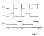
e) un circuit de commutation (23) couplé entre ladite pluralité de paires de lignes de bit et une source d'un premier niveau logique, et sensible à des deuxième et troisième signaux d'horloge externe (CLK2,CLK3) élevés alternativement à un niveau actif en synchronisme avec ledit premier signal d'horloge externe (CLK1), pour fournir alternativement ledit premier niveau logique à des lignes de bit constitutives de ladite pluralité de paires de lignes de bit. - Dispositif de mémoire dynamique à accès sélectif selon la revendication 3, dans lequel ledit circuit de commutation (23) comprend :e-1) une pluralité de premiers transistors de commutation (Q21,Q23,Q25), chacun étant couplé entre ladite source d'un premier niveau logique et l'une des lignes de bit constitutives de chaque paire de lignes de bit, et sensibles à l'un desdits deuxième et troisième signaux d'horloge externe, ete-2) une pluralité de seconds transistors de commutation (Q22,Q24,Q26), chacun étant couplé entre ladite source d'un premier niveau logique et l'autre des lignes de bit constitutives de ladite chaque paire de lignes de bit, et sensibles à l'autre desdits deuxième et troisième signaux d'horloge externe.
Applications Claiming Priority (2)
| Application Number | Priority Date | Filing Date | Title |
|---|---|---|---|
| JP115563/91 | 1991-04-19 | ||
| JP11556391A JP3237127B2 (ja) | 1991-04-19 | 1991-04-19 | ダイナミックランダムアクセスメモリ装置 |
Publications (2)
| Publication Number | Publication Date |
|---|---|
| EP0509360A1 EP0509360A1 (fr) | 1992-10-21 |
| EP0509360B1 true EP0509360B1 (fr) | 1997-07-23 |
Family
ID=14665646
Family Applications (1)
| Application Number | Title | Priority Date | Filing Date |
|---|---|---|---|
| EP92105926A Expired - Lifetime EP0509360B1 (fr) | 1991-04-19 | 1992-04-06 | Dispositif de mémoire à accès sélectif muni d'un sélecteur à multiple ligne des mots usé dans un test de marquage à chaud |
Country Status (5)
| Country | Link |
|---|---|
| US (1) | US5293340A (fr) |
| EP (1) | EP0509360B1 (fr) |
| JP (1) | JP3237127B2 (fr) |
| KR (1) | KR950014247B1 (fr) |
| DE (1) | DE69221005T2 (fr) |
Families Citing this family (20)
| Publication number | Priority date | Publication date | Assignee | Title |
|---|---|---|---|---|
| JP2793427B2 (ja) * | 1992-04-08 | 1998-09-03 | 株式会社東芝 | 半導体装置 |
| JPH0628861A (ja) * | 1992-07-07 | 1994-02-04 | Oki Electric Ind Co Ltd | 半導体記憶装置 |
| DE4223532A1 (de) * | 1992-07-17 | 1994-01-20 | Philips Patentverwaltung | Schaltungsanordnung zum Prüfen der Adressierung wenigstens einer Matrix |
| KR970010658B1 (ko) * | 1993-11-26 | 1997-06-30 | 삼성전자 주식회사 | 번-인회로를 가지는 반도체메모리장치 및 그 번-인방법 |
| DE69516768T2 (de) * | 1994-03-09 | 2000-11-23 | Koninkl Philips Electronics Nv | Prüfbarer i ddq- speicher durch kumulative wort-zeilen-aktivierung |
| US5440517A (en) * | 1994-08-15 | 1995-08-08 | Micron Technology, Inc. | DRAMs having on-chip row copy circuits for use in testing and video imaging and method for operating same |
| JP3734853B2 (ja) * | 1995-06-27 | 2006-01-11 | 株式会社ルネサステクノロジ | 半導体記憶装置 |
| US6209071B1 (en) | 1996-05-07 | 2001-03-27 | Rambus Inc. | Asynchronous request/synchronous data dynamic random access memory |
| US5835628A (en) * | 1996-11-21 | 1998-11-10 | Xerox Corporation | Method and system for generating histograms from a scanned image |
| US5881166A (en) * | 1996-11-21 | 1999-03-09 | Xerox Corporation | Method and system for generating a histogram of a scanned image |
| US5751848A (en) * | 1996-11-21 | 1998-05-12 | Xerox Corporation | System and method for generating and utilizing histogram data from a scanned image |
| US5848183A (en) * | 1996-11-21 | 1998-12-08 | Xerox Corporation | System and method for generating and utilizing histogram data from a scanned image |
| US6263448B1 (en) | 1997-10-10 | 2001-07-17 | Rambus Inc. | Power control system for synchronous memory device |
| JP3938229B2 (ja) * | 1997-10-13 | 2007-06-27 | 沖電気工業株式会社 | 半導体記憶装置 |
| JPH11154103A (ja) * | 1997-11-20 | 1999-06-08 | Mitsubishi Electric Corp | 半導体集積回路装置 |
| US6453258B1 (en) | 1999-12-17 | 2002-09-17 | International Business Machines Corporation | Optimized burn-in for fixed time dynamic logic circuitry |
| US6618171B1 (en) | 2000-02-25 | 2003-09-09 | Xerox Corporation | Black point adjustment based on image background |
| US7106644B2 (en) * | 2003-12-01 | 2006-09-12 | Elite Semiconductor Memory Technology, Inc. | Memory device and method for burn-in test |
| CN100421184C (zh) * | 2004-03-03 | 2008-09-24 | 晶豪科技股份有限公司 | 用于预烧测试的存储器装置以及方法 |
| FR3059114B1 (fr) * | 2016-11-23 | 2019-01-25 | Continental Automotive France | Procede de diagnostic d'une alimentation de polarisation pour un systeme d'acquisition comprenant un dispositif matriciel d'interface |
Family Cites Families (8)
| Publication number | Priority date | Publication date | Assignee | Title |
|---|---|---|---|---|
| DD137504A1 (de) * | 1978-07-03 | 1979-09-05 | Gunther Schneegass | Schaltungsanordnung zur pruefung von halbleiterspeichern |
| US4380805A (en) * | 1980-09-08 | 1983-04-19 | Mostek Corporation | Tape burn-in circuit |
| JPS61289600A (ja) * | 1985-06-17 | 1986-12-19 | Fujitsu Ltd | 半導体記憶装置 |
| JPS62177799A (ja) * | 1986-01-30 | 1987-08-04 | Toshiba Corp | 半導体記憶装置 |
| EP0264893B1 (fr) * | 1986-10-20 | 1995-01-18 | Nippon Telegraph And Telephone Corporation | Mémoire à semi-conducteur |
| US4751679A (en) * | 1986-12-22 | 1988-06-14 | Motorola, Inc. | Gate stress test of a MOS memory |
| JPH01113999A (ja) * | 1987-10-28 | 1989-05-02 | Toshiba Corp | 不揮発性メモリのストレステスト回路 |
| JPH01208795A (ja) * | 1988-02-16 | 1989-08-22 | Toshiba Corp | 半導体記憶装置 |
-
1991
- 1991-04-19 JP JP11556391A patent/JP3237127B2/ja not_active Expired - Lifetime
-
1992
- 1992-04-06 EP EP92105926A patent/EP0509360B1/fr not_active Expired - Lifetime
- 1992-04-06 DE DE69221005T patent/DE69221005T2/de not_active Expired - Lifetime
- 1992-04-13 US US07/867,361 patent/US5293340A/en not_active Expired - Lifetime
- 1992-04-16 KR KR1019920006337A patent/KR950014247B1/ko not_active IP Right Cessation
Also Published As
| Publication number | Publication date |
|---|---|
| DE69221005D1 (de) | 1997-08-28 |
| JP3237127B2 (ja) | 2001-12-10 |
| JPH04321252A (ja) | 1992-11-11 |
| KR920020508A (ko) | 1992-11-21 |
| EP0509360A1 (fr) | 1992-10-21 |
| US5293340A (en) | 1994-03-08 |
| DE69221005T2 (de) | 1998-02-26 |
| KR950014247B1 (ko) | 1995-11-23 |
Similar Documents
| Publication | Publication Date | Title |
|---|---|---|
| EP0509360B1 (fr) | Dispositif de mémoire à accès sélectif muni d'un sélecteur à multiple ligne des mots usé dans un test de marquage à chaud | |
| KR960002010B1 (ko) | 반도체 기억 장치 | |
| EP0565079B1 (fr) | Dispositif semi-conducteur comprenant un arrangement de mise en court-circuit pour un test de tension | |
| KR960000888B1 (ko) | 반도체 기억 장치 | |
| KR950001133B1 (ko) | 스태틱형 반도체 기억장치 | |
| KR0135108B1 (ko) | 스트레스 테스트 회로를 포함하는 반도체 메모리 장치 | |
| KR960000721B1 (ko) | 반도체 기억장치 | |
| JPH0855497A (ja) | 半導体メモリ装置のバーンインテスト回路 | |
| EP0585870A2 (fr) | Mémoire dynamique à accès aléatoire comportant un circuit d'application de tension élevée | |
| EP0492609B1 (fr) | Dispositif à semi-conducteur comprenant des plages de test en tension élevée | |
| US5986917A (en) | Wafer burn-in test circuit for a semiconductor memory device | |
| US6185138B1 (en) | Method and apparatus for testing random access memory devices | |
| EP0456254B1 (fr) | Dispositf à semi-conducteurs et méthode pour l'examiner | |
| JP3803145B2 (ja) | 半導体メモリ装置のバーンインテスト回路及び方法 | |
| KR950002295B1 (ko) | 반도체 기억 장치 | |
| US6490223B1 (en) | Integrated circuit capable of being burn-in tested using an alternating current stress and a testing method using the same | |
| US6414888B2 (en) | Semiconductor storage device having burn-in mode | |
| JP3762517B2 (ja) | 半導体メモリ装置のバーンインストレス回路 | |
| KR950011730B1 (ko) | 동적 랜덤 액세스 메모리 장치 | |
| JPH09320296A (ja) | 半導体記憶装置 | |
| KR20050072677A (ko) | 반도체 메모리 장치 | |
| JP4558186B2 (ja) | 半導体装置 | |
| JPH04258880A (ja) | 半導体記憶装置 | |
| JPH07220498A (ja) | 半導体記憶装置 | |
| KR19980056185A (ko) | 반도체 메모리소자의 워드라인 구동회로 |
Legal Events
| Date | Code | Title | Description |
|---|---|---|---|
| PUAI | Public reference made under article 153(3) epc to a published international application that has entered the european phase |
Free format text: ORIGINAL CODE: 0009012 |
|
| 17P | Request for examination filed |
Effective date: 19920406 |
|
| AK | Designated contracting states |
Kind code of ref document: A1 Designated state(s): DE FR GB |
|
| 17Q | First examination report despatched |
Effective date: 19950922 |
|
| GRAG | Despatch of communication of intention to grant |
Free format text: ORIGINAL CODE: EPIDOS AGRA |
|
| GRAH | Despatch of communication of intention to grant a patent |
Free format text: ORIGINAL CODE: EPIDOS IGRA |
|
| GRAH | Despatch of communication of intention to grant a patent |
Free format text: ORIGINAL CODE: EPIDOS IGRA |
|
| GRAA | (expected) grant |
Free format text: ORIGINAL CODE: 0009210 |
|
| AK | Designated contracting states |
Kind code of ref document: B1 Designated state(s): DE FR GB |
|
| REF | Corresponds to: |
Ref document number: 69221005 Country of ref document: DE Date of ref document: 19970828 |
|
| ET | Fr: translation filed | ||
| PLBE | No opposition filed within time limit |
Free format text: ORIGINAL CODE: 0009261 |
|
| STAA | Information on the status of an ep patent application or granted ep patent |
Free format text: STATUS: NO OPPOSITION FILED WITHIN TIME LIMIT |
|
| 26N | No opposition filed | ||
| REG | Reference to a national code |
Ref country code: GB Ref legal event code: IF02 |
|
| REG | Reference to a national code |
Ref country code: GB Ref legal event code: 732E |
|
| REG | Reference to a national code |
Ref country code: FR Ref legal event code: TQ |
|
| REG | Reference to a national code |
Ref country code: GB Ref legal event code: 732E |
|
| REG | Reference to a national code |
Ref country code: FR Ref legal event code: TP Ref country code: FR Ref legal event code: TQ |
|
| PGFP | Annual fee paid to national office [announced via postgrant information from national office to epo] |
Ref country code: GB Payment date: 20090401 Year of fee payment: 18 |
|
| GBPC | Gb: european patent ceased through non-payment of renewal fee |
Effective date: 20100406 |
|
| PG25 | Lapsed in a contracting state [announced via postgrant information from national office to epo] |
Ref country code: GB Free format text: LAPSE BECAUSE OF NON-PAYMENT OF DUE FEES Effective date: 20100406 |
|
| PGFP | Annual fee paid to national office [announced via postgrant information from national office to epo] |
Ref country code: DE Payment date: 20110330 Year of fee payment: 20 Ref country code: FR Payment date: 20110426 Year of fee payment: 20 |
|
| REG | Reference to a national code |
Ref country code: DE Ref legal event code: R071 Ref document number: 69221005 Country of ref document: DE |
|
| REG | Reference to a national code |
Ref country code: DE Ref legal event code: R071 Ref document number: 69221005 Country of ref document: DE |
|
| PG25 | Lapsed in a contracting state [announced via postgrant information from national office to epo] |
Ref country code: DE Free format text: LAPSE BECAUSE OF EXPIRATION OF PROTECTION Effective date: 20120407 |