EP0498392A2 - IC-Speicherkartensystem - Google Patents
IC-Speicherkartensystem Download PDFInfo
- Publication number
- EP0498392A2 EP0498392A2 EP92101894A EP92101894A EP0498392A2 EP 0498392 A2 EP0498392 A2 EP 0498392A2 EP 92101894 A EP92101894 A EP 92101894A EP 92101894 A EP92101894 A EP 92101894A EP 0498392 A2 EP0498392 A2 EP 0498392A2
- Authority
- EP
- European Patent Office
- Prior art keywords
- memory card
- data
- host processor
- signal
- address
- Prior art date
- Legal status (The legal status is an assumption and is not a legal conclusion. Google has not performed a legal analysis and makes no representation as to the accuracy of the status listed.)
- Granted
Links
Images

Classifications
-
- G—PHYSICS
- G11—INFORMATION STORAGE
- G11C—STATIC STORES
- G11C16/00—Erasable programmable read-only memories
- G11C16/02—Erasable programmable read-only memories electrically programmable
- G11C16/06—Auxiliary circuits, e.g. for writing into memory
- G11C16/10—Programming or data input circuits
- G11C16/102—External programming circuits, e.g. EPROM programmers; In-circuit programming or reprogramming; EPROM emulators
Definitions
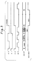
- An address control 504 is incorporated in the memory chip 500.
- the I/O section 400 accesses the leading address of particular one of the blocks #1-#n while the address control 504 sequentially increments the address of the block, whereby data are sequentially written to or read out of the block of interest.
- a command ROM 506 delivers a write command or a read command to the EEPROM cell 502. Data read out of any one of the blocks #1-#n is sent to the host processor 100 via a buffer 508. Data to be written in any one of the blocks #1-#n is transferred to the block via the buffer 508.
- the state signals A0 and A1, erase signal A2 and write signal WR or read signal RD from the host processor 100 are applied to the mode decoder 406 via the connector 360.
- the mode decoder 406 outputs an erase mode signal Se, a write mode signal Sw or a read mode signal Sr and select signals Ss for activating the registers of the address latch 402.
- the mode decoder 406 delivers a select signal Ss for activating a first register included in the address latch 402.
- the address latch 402 latches a lower address represented by eight bits.
- the host processor 100 sends the next eight bits of data to the memory card 200.
- the write signal WR goes high.
- the mode decoder 406 again delivers the write signal Sw to the write sequencer 410 to cause it to write the eight bits of data in the same block as the previous eight bits of data. In this manner, data sequentially sent from the host processor 100 are written to the successive addresses of the designated block.
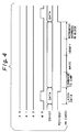
- the IC memory card 200 has been assumed to be of the type incorporating an EEPROM, it may be replaced with an IC memory card having a built-in SRAM.
- the host processor 100 operates in the above-described manner even with an IC memory card having an SRAM, it neglects the erase signal A2 since the erase terminal 19 is not connected to the inside of such a memory card.
- the memory card 200 writes the data over the data existing in the block which is designated by the address.
Landscapes
- Read Only Memory (AREA)
Applications Claiming Priority (2)
| Application Number | Priority Date | Filing Date | Title |
|---|---|---|---|
| JP36539/91 | 1991-02-07 | ||
| JP3036539A JP2724046B2 (ja) | 1991-02-07 | 1991-02-07 | Icメモリカードシステム |
Publications (3)
| Publication Number | Publication Date |
|---|---|
| EP0498392A2 true EP0498392A2 (de) | 1992-08-12 |
| EP0498392A3 EP0498392A3 (de) | 1994-02-16 |
| EP0498392B1 EP0498392B1 (de) | 1997-01-15 |
Family
ID=12472589
Family Applications (1)
| Application Number | Title | Priority Date | Filing Date |
|---|---|---|---|
| EP92101894A Expired - Lifetime EP0498392B1 (de) | 1991-02-07 | 1992-02-05 | IC-Speicherkartensystem |
Country Status (4)
| Country | Link |
|---|---|
| US (1) | US5548741A (de) |
| EP (1) | EP0498392B1 (de) |
| JP (1) | JP2724046B2 (de) |
| DE (1) | DE69216646T2 (de) |
Cited By (1)
| Publication number | Priority date | Publication date | Assignee | Title |
|---|---|---|---|---|
| WO2001059788A1 (fr) * | 2000-02-11 | 2001-08-16 | Gemplus | Ecriture en temps reel securisee pour memoire volatile |
Families Citing this family (41)
| Publication number | Priority date | Publication date | Assignee | Title |
|---|---|---|---|---|
| JP4341043B2 (ja) * | 1995-03-06 | 2009-10-07 | 真彦 久野 | I/o拡張装置,外部記憶装置,この外部記憶装置へのアクセス方法及び装置 |
| KR100232231B1 (ko) * | 1996-09-13 | 2000-03-02 | 김영환 | 비휘발성 메모리 소자의 데이터 기입 장치 및 방법 |
| US6229737B1 (en) | 1996-12-12 | 2001-05-08 | Ericsson Inc. | Method and apparatus for initializing semiconductor memory |
| US6000006A (en) * | 1997-08-25 | 1999-12-07 | Bit Microsystems, Inc. | Unified re-map and cache-index table with dual write-counters for wear-leveling of non-volatile flash RAM mass storage |
| US5974500A (en) * | 1997-11-14 | 1999-10-26 | Atmel Corporation | Memory device having programmable access protection and method of operating the same |
| JP2001167586A (ja) * | 1999-12-08 | 2001-06-22 | Toshiba Corp | 不揮発性半導体メモリ装置 |
| US7698502B2 (en) * | 2002-07-24 | 2010-04-13 | Seagate Technology Llc | File recovery system for a removable portable memory device |
| US7487287B2 (en) * | 2006-02-08 | 2009-02-03 | Atmel Corporation | Time efficient embedded EEPROM/processor control method |
| KR100845525B1 (ko) * | 2006-08-07 | 2008-07-10 | 삼성전자주식회사 | 메모리 카드 시스템, 그것의 데이터 전송 방법, 그리고반도체 메모리 장치 |
| JP2009059253A (ja) * | 2007-08-31 | 2009-03-19 | Sony Corp | カード型周辺装置 |
| JP4438846B2 (ja) * | 2007-09-14 | 2010-03-24 | ソニー株式会社 | カード型周辺装置 |
| US8959307B1 (en) | 2007-11-16 | 2015-02-17 | Bitmicro Networks, Inc. | Reduced latency memory read transactions in storage devices |
| US8665601B1 (en) | 2009-09-04 | 2014-03-04 | Bitmicro Networks, Inc. | Solid state drive with improved enclosure assembly |
| US9135190B1 (en) | 2009-09-04 | 2015-09-15 | Bitmicro Networks, Inc. | Multi-profile memory controller for computing devices |
| US8447908B2 (en) | 2009-09-07 | 2013-05-21 | Bitmicro Networks, Inc. | Multilevel memory bus system for solid-state mass storage |
| US8560804B2 (en) | 2009-09-14 | 2013-10-15 | Bitmicro Networks, Inc. | Reducing erase cycles in an electronic storage device that uses at least one erase-limited memory device |
| JP2012190195A (ja) * | 2011-03-09 | 2012-10-04 | Fujitsu Ltd | 制御装置 |
| US9372755B1 (en) | 2011-10-05 | 2016-06-21 | Bitmicro Networks, Inc. | Adaptive power cycle sequences for data recovery |
| US9043669B1 (en) | 2012-05-18 | 2015-05-26 | Bitmicro Networks, Inc. | Distributed ECC engine for storage media |
| US9423457B2 (en) | 2013-03-14 | 2016-08-23 | Bitmicro Networks, Inc. | Self-test solution for delay locked loops |
| US9842024B1 (en) | 2013-03-15 | 2017-12-12 | Bitmicro Networks, Inc. | Flash electronic disk with RAID controller |
| US9934045B1 (en) | 2013-03-15 | 2018-04-03 | Bitmicro Networks, Inc. | Embedded system boot from a storage device |
| US9916213B1 (en) | 2013-03-15 | 2018-03-13 | Bitmicro Networks, Inc. | Bus arbitration with routing and failover mechanism |
| US9858084B2 (en) | 2013-03-15 | 2018-01-02 | Bitmicro Networks, Inc. | Copying of power-on reset sequencer descriptor from nonvolatile memory to random access memory |
| US9734067B1 (en) | 2013-03-15 | 2017-08-15 | Bitmicro Networks, Inc. | Write buffering |
| US9798688B1 (en) | 2013-03-15 | 2017-10-24 | Bitmicro Networks, Inc. | Bus arbitration with routing and failover mechanism |
| US9672178B1 (en) | 2013-03-15 | 2017-06-06 | Bitmicro Networks, Inc. | Bit-mapped DMA transfer with dependency table configured to monitor status so that a processor is not rendered as a bottleneck in a system |
| US9720603B1 (en) | 2013-03-15 | 2017-08-01 | Bitmicro Networks, Inc. | IOC to IOC distributed caching architecture |
| US10489318B1 (en) | 2013-03-15 | 2019-11-26 | Bitmicro Networks, Inc. | Scatter-gather approach for parallel data transfer in a mass storage system |
| US9430386B2 (en) | 2013-03-15 | 2016-08-30 | Bitmicro Networks, Inc. | Multi-leveled cache management in a hybrid storage system |
| US9875205B1 (en) | 2013-03-15 | 2018-01-23 | Bitmicro Networks, Inc. | Network of memory systems |
| US9400617B2 (en) | 2013-03-15 | 2016-07-26 | Bitmicro Networks, Inc. | Hardware-assisted DMA transfer with dependency table configured to permit-in parallel-data drain from cache without processor intervention when filled or drained |
| US9971524B1 (en) | 2013-03-15 | 2018-05-15 | Bitmicro Networks, Inc. | Scatter-gather approach for parallel data transfer in a mass storage system |
| US9501436B1 (en) | 2013-03-15 | 2016-11-22 | Bitmicro Networks, Inc. | Multi-level message passing descriptor |
| US10078604B1 (en) | 2014-04-17 | 2018-09-18 | Bitmicro Networks, Inc. | Interrupt coalescing |
| US9952991B1 (en) | 2014-04-17 | 2018-04-24 | Bitmicro Networks, Inc. | Systematic method on queuing of descriptors for multiple flash intelligent DMA engine operation |
| US9811461B1 (en) | 2014-04-17 | 2017-11-07 | Bitmicro Networks, Inc. | Data storage system |
| US10025736B1 (en) | 2014-04-17 | 2018-07-17 | Bitmicro Networks, Inc. | Exchange message protocol message transmission between two devices |
| US10042792B1 (en) | 2014-04-17 | 2018-08-07 | Bitmicro Networks, Inc. | Method for transferring and receiving frames across PCI express bus for SSD device |
| US10055150B1 (en) | 2014-04-17 | 2018-08-21 | Bitmicro Networks, Inc. | Writing volatile scattered memory metadata to flash device |
| US10552050B1 (en) | 2017-04-07 | 2020-02-04 | Bitmicro Llc | Multi-dimensional computer storage system |
Citations (2)
| Publication number | Priority date | Publication date | Assignee | Title |
|---|---|---|---|---|
| WO1990003033A1 (fr) * | 1988-09-14 | 1990-03-22 | Sgs Thomson Microelectronics S.A. | Memoire eprom avec signature interne concernant notamment le mode de programmation |
| EP0408002A2 (de) * | 1989-07-11 | 1991-01-16 | Fujitsu Limited | Programmierbare Halbleiterspeicheranordnung |
Family Cites Families (15)
| Publication number | Priority date | Publication date | Assignee | Title |
|---|---|---|---|---|
| JPS6174200A (ja) * | 1984-09-20 | 1986-04-16 | Nec Corp | Eeprom搭載カ−ド |
| JPS62121979A (ja) * | 1985-11-22 | 1987-06-03 | Mitsubishi Electric Corp | 集積回路メモリ |
| US4931997A (en) * | 1987-03-16 | 1990-06-05 | Hitachi Ltd. | Semiconductor memory having storage buffer to save control data during bulk erase |
| JPH0758502B2 (ja) * | 1988-06-30 | 1995-06-21 | 三菱電機株式会社 | Icカード |
| JPH02177092A (ja) * | 1988-12-27 | 1990-07-10 | Nec Corp | Eeprom集積回路装置 |
| FR2641757A1 (fr) * | 1989-01-13 | 1990-07-20 | Rerolle Gerard | Kayak insubmersible |
| JPH02278596A (ja) * | 1989-04-18 | 1990-11-14 | Toshiba Corp | 半導体記憶装置 |
| JP2745669B2 (ja) * | 1989-04-27 | 1998-04-28 | ブラザー工業株式会社 | プリンタ |
| JP3226271B2 (ja) * | 1989-07-27 | 2001-11-05 | オリンパス光学工業株式会社 | ディジタル電子スチルカメラ |
| JPH03240127A (ja) * | 1990-02-17 | 1991-10-25 | Hitachi Maxell Ltd | プログラム制御システム |
| JP2784550B2 (ja) * | 1990-03-05 | 1998-08-06 | 三菱電機株式会社 | 半導体記憶装置 |
| US5016223A (en) * | 1990-04-17 | 1991-05-14 | Mitsubishi Denki Kabushiki Kaisha | Memory card circuit |
| US5303198A (en) * | 1990-09-28 | 1994-04-12 | Fuji Photo Film Co., Ltd. | Method of recording data in memory card having EEPROM and memory card system using the same |
| JPH04137081A (ja) * | 1990-09-28 | 1992-05-12 | Fuji Photo Film Co Ltd | Eepromを有するicメモリカード |
| US5208732A (en) * | 1991-05-29 | 1993-05-04 | Texas Instruments, Incorporated | Memory card with flexible conductor between substrate and metal cover |
-
1991
- 1991-02-07 JP JP3036539A patent/JP2724046B2/ja not_active Expired - Fee Related
-
1992
- 1992-02-05 DE DE69216646T patent/DE69216646T2/de not_active Expired - Fee Related
- 1992-02-05 EP EP92101894A patent/EP0498392B1/de not_active Expired - Lifetime
-
1995
- 1995-02-13 US US08/387,376 patent/US5548741A/en not_active Expired - Lifetime
Patent Citations (2)
| Publication number | Priority date | Publication date | Assignee | Title |
|---|---|---|---|---|
| WO1990003033A1 (fr) * | 1988-09-14 | 1990-03-22 | Sgs Thomson Microelectronics S.A. | Memoire eprom avec signature interne concernant notamment le mode de programmation |
| EP0408002A2 (de) * | 1989-07-11 | 1991-01-16 | Fujitsu Limited | Programmierbare Halbleiterspeicheranordnung |
Cited By (2)
| Publication number | Priority date | Publication date | Assignee | Title |
|---|---|---|---|---|
| WO2001059788A1 (fr) * | 2000-02-11 | 2001-08-16 | Gemplus | Ecriture en temps reel securisee pour memoire volatile |
| FR2805073A1 (fr) * | 2000-02-11 | 2001-08-17 | Gemplus Card Int | Ecriture en temps reel securisee pour memoire non volatile |
Also Published As
| Publication number | Publication date |
|---|---|
| JP2724046B2 (ja) | 1998-03-09 |
| EP0498392A3 (de) | 1994-02-16 |
| US5548741A (en) | 1996-08-20 |
| DE69216646T2 (de) | 1997-05-07 |
| DE69216646D1 (de) | 1997-02-27 |
| JPH04256088A (ja) | 1992-09-10 |
| EP0498392B1 (de) | 1997-01-15 |
Similar Documents
| Publication | Publication Date | Title |
|---|---|---|
| EP0498392B1 (de) | IC-Speicherkartensystem | |
| US5361228A (en) | IC memory card system having a common data and address bus | |
| US6434658B1 (en) | Memory device operable with a small-capacity buffer memory and having a flash memory | |
| EP0528280B1 (de) | Aufzeichnungsgerät für eine Speicherkarte | |
| EP0712067B1 (de) | Flashspeicherkarte | |
| US5303198A (en) | Method of recording data in memory card having EEPROM and memory card system using the same | |
| US5386539A (en) | IC memory card comprising an EEPROM with data and address buffering for controlling the writing/reading of data to EEPROM | |
| JP3718578B2 (ja) | メモリ管理方法及びメモリ管理装置 | |
| US5890188A (en) | Nonvolatile semiconductor memory device having means for selective transfer of memory block contents and for chaining together unused memory blocks | |
| JP4165990B2 (ja) | メモリコントローラ及びメモリコントローラを備えるフラッシュメモリシステム、並びに、フラッシュメモリへのデータの書き込み方法 | |
| US6154808A (en) | Method and apparatus for controlling data erase operations of a non-volatile memory device | |
| US7123519B2 (en) | Storage device employing a flash memory | |
| JPH08263361A (ja) | フラッシュメモリカード | |
| US5604917A (en) | IC memory card having masking function for preventing writing of data into a fixed memory area | |
| US5724544A (en) | IC memory card utilizing dual eeproms for image and management data | |
| CN101471124B (zh) | 存储卡和搭载在存储卡中的卡用控制器以及存储卡的处理装置 | |
| JPWO2002052416A1 (ja) | フラッシュメモリシステム | |
| JP2768618B2 (ja) | 半導体ディスク装置 | |
| EP0890955A2 (de) | Speichervorrichtung sowie Datenlese- und Schreibverfahren | |
| EP0615193A1 (de) | Speicherkartenvorrichtung. | |
| US5829014A (en) | Method of supervising storage of data in a memory card having EEPROM and a memory card system using the same | |
| JP3017524B2 (ja) | Icメモリカードにおけるデータ記録方法およびicメモリカードシステム | |
| JP3117244B2 (ja) | Eepromの制御装置 | |
| JPH05150913A (ja) | フラツシユメモリを記憶媒体としたシリコンデイスク | |
| JP2584119B2 (ja) | メモリカードにおけるデータ記録方法およびメモリカードシステム |
Legal Events
| Date | Code | Title | Description |
|---|---|---|---|
| PUAI | Public reference made under article 153(3) epc to a published international application that has entered the european phase |
Free format text: ORIGINAL CODE: 0009012 |
|
| AK | Designated contracting states |
Kind code of ref document: A2 Designated state(s): DE GB |
|
| PUAL | Search report despatched |
Free format text: ORIGINAL CODE: 0009013 |
|
| AK | Designated contracting states |
Kind code of ref document: A3 Designated state(s): DE GB |
|
| 17P | Request for examination filed |
Effective date: 19940323 |
|
| GRAG | Despatch of communication of intention to grant |
Free format text: ORIGINAL CODE: EPIDOS AGRA |
|
| 17Q | First examination report despatched |
Effective date: 19960423 |
|
| GRAH | Despatch of communication of intention to grant a patent |
Free format text: ORIGINAL CODE: EPIDOS IGRA |
|
| GRAH | Despatch of communication of intention to grant a patent |
Free format text: ORIGINAL CODE: EPIDOS IGRA |
|
| GRAA | (expected) grant |
Free format text: ORIGINAL CODE: 0009210 |
|
| AK | Designated contracting states |
Kind code of ref document: B1 Designated state(s): DE GB |
|
| REF | Corresponds to: |
Ref document number: 69216646 Country of ref document: DE Date of ref document: 19970227 |
|
| PLBE | No opposition filed within time limit |
Free format text: ORIGINAL CODE: 0009261 |
|
| STAA | Information on the status of an ep patent application or granted ep patent |
Free format text: STATUS: NO OPPOSITION FILED WITHIN TIME LIMIT |
|
| 26N | No opposition filed | ||
| REG | Reference to a national code |
Ref country code: GB Ref legal event code: IF02 |
|
| REG | Reference to a national code |
Ref country code: GB Ref legal event code: 732E |
|
| PGFP | Annual fee paid to national office [announced via postgrant information from national office to epo] |
Ref country code: DE Payment date: 20090129 Year of fee payment: 18 |
|
| PGFP | Annual fee paid to national office [announced via postgrant information from national office to epo] |
Ref country code: GB Payment date: 20090204 Year of fee payment: 18 |
|
| GBPC | Gb: european patent ceased through non-payment of renewal fee |
Effective date: 20100205 |
|
| PG25 | Lapsed in a contracting state [announced via postgrant information from national office to epo] |
Ref country code: DE Free format text: LAPSE BECAUSE OF NON-PAYMENT OF DUE FEES Effective date: 20100901 |
|
| PG25 | Lapsed in a contracting state [announced via postgrant information from national office to epo] |
Ref country code: GB Free format text: LAPSE BECAUSE OF NON-PAYMENT OF DUE FEES Effective date: 20100205 |