US6434658B1 - Memory device operable with a small-capacity buffer memory and having a flash memory - Google Patents
Memory device operable with a small-capacity buffer memory and having a flash memory Download PDFInfo
- Publication number
- US6434658B1 US6434658B1 US09/395,941 US39594199A US6434658B1 US 6434658 B1 US6434658 B1 US 6434658B1 US 39594199 A US39594199 A US 39594199A US 6434658 B1 US6434658 B1 US 6434658B1
- Authority
- US
- United States
- Prior art keywords
- data
- external
- read
- write
- internal
- Prior art date
- Legal status (The legal status is an assumption and is not a legal conclusion. Google has not performed a legal analysis and makes no representation as to the accuracy of the status listed.)
- Expired - Fee Related
Links
Images


Classifications
-
- G—PHYSICS
- G06—COMPUTING; CALCULATING OR COUNTING
- G06F—ELECTRIC DIGITAL DATA PROCESSING
- G06F3/00—Input arrangements for transferring data to be processed into a form capable of being handled by the computer; Output arrangements for transferring data from processing unit to output unit, e.g. interface arrangements
- G06F3/06—Digital input from, or digital output to, record carriers, e.g. RAID, emulated record carriers or networked record carriers
- G06F3/0601—Interfaces specially adapted for storage systems
- G06F3/0602—Interfaces specially adapted for storage systems specifically adapted to achieve a particular effect
- G06F3/0626—Reducing size or complexity of storage systems
-
- G—PHYSICS
- G06—COMPUTING; CALCULATING OR COUNTING
- G06F—ELECTRIC DIGITAL DATA PROCESSING
- G06F12/00—Accessing, addressing or allocating within memory systems or architectures
- G06F12/02—Addressing or allocation; Relocation
- G06F12/0223—User address space allocation, e.g. contiguous or non contiguous base addressing
- G06F12/023—Free address space management
- G06F12/0238—Memory management in non-volatile memory, e.g. resistive RAM or ferroelectric memory
- G06F12/0246—Memory management in non-volatile memory, e.g. resistive RAM or ferroelectric memory in block erasable memory, e.g. flash memory
-
- G—PHYSICS
- G06—COMPUTING; CALCULATING OR COUNTING
- G06F—ELECTRIC DIGITAL DATA PROCESSING
- G06F3/00—Input arrangements for transferring data to be processed into a form capable of being handled by the computer; Output arrangements for transferring data from processing unit to output unit, e.g. interface arrangements
- G06F3/06—Digital input from, or digital output to, record carriers, e.g. RAID, emulated record carriers or networked record carriers
- G06F3/0601—Interfaces specially adapted for storage systems
- G06F3/0628—Interfaces specially adapted for storage systems making use of a particular technique
- G06F3/0655—Vertical data movement, i.e. input-output transfer; data movement between one or more hosts and one or more storage devices
- G06F3/0656—Data buffering arrangements
-
- G—PHYSICS
- G06—COMPUTING; CALCULATING OR COUNTING
- G06F—ELECTRIC DIGITAL DATA PROCESSING
- G06F3/00—Input arrangements for transferring data to be processed into a form capable of being handled by the computer; Output arrangements for transferring data from processing unit to output unit, e.g. interface arrangements
- G06F3/06—Digital input from, or digital output to, record carriers, e.g. RAID, emulated record carriers or networked record carriers
- G06F3/0601—Interfaces specially adapted for storage systems
- G06F3/0668—Interfaces specially adapted for storage systems adopting a particular infrastructure
- G06F3/0671—In-line storage system
- G06F3/0673—Single storage device
- G06F3/0679—Non-volatile semiconductor memory device, e.g. flash memory, one time programmable memory [OTP]
-
- G—PHYSICS
- G06—COMPUTING; CALCULATING OR COUNTING
- G06F—ELECTRIC DIGITAL DATA PROCESSING
- G06F2212/00—Indexing scheme relating to accessing, addressing or allocation within memory systems or architectures
- G06F2212/72—Details relating to flash memory management
- G06F2212/7203—Temporary buffering, e.g. using volatile buffer or dedicated buffer blocks
Definitions
- the present invention relates to a memory device, and more specifically, to a memory device having a flash memory.
- a flash memory is a non-volatile, rewritable semiconductor memory device that allows the erase operation of data one section at a time.
- the flash memory integrates storage elements at a high density, and, in order to enable a fast-speed data transmission and reception, specifies a sector address, and reads, erases, and writes (programs) a certain amount of data one sector at a time.
- program refers to setting the state of a memory cell in a flash memory to correspond to the value of either 1 or 0 according to data provided from outside.
- the sector capacity the unit of data the flash memory reads out at one time, tends to increase in size as well. For instance, in an AND-type flash memory of 256 Mbits, the sector capacity is 2048 bytes.
- the data capacity (hereinafter referred to as a medium sector capacity), which is a unit of data the informational equipment such as a personal computer transmits to and receives from a memory device such as a hard disk or a memory card, is normally 512 bytes, for example, and no such tendency to increase in the medium sector capacity is noted in particular.
- a buffer memory for temporarily storing sector data of a flash memory and for adjusting the timing and the capacity for the data transfer between the memory device and the host system.
- SRAM Static Random Access Memory
- the buffer memory was required to be have a capacity of the same or a larger size than the sector capacity of the flash memory even when the capacity of data transfer between the memory device and the host system, i.e. the medium sector capacity, was smaller than the sector capacity of the flash memory.
- An object of the present invention is to provide a memory device having a flash memory that allows the incorporation of a buffer memory of a small capacity equivalent to the medium sector capacity as well as the reduction in cost.
- the present invention is a memory device with a flash memory and having a write mode in which data is stored upon the reception of an external write address signal and an external write data train from a host system, and including a flash memory and a data input/output portion.
- the flash memory in the data erase operation, a memory region holding a prescribed number of bits of data is erased at one time as the smallest unit, and in the write mode an internal write data train having a prescribed data length is written according to an internal write address signal.
- the data input/output portion receives the external write address signal and generates an internal write address signal, receives and retains the external write data train, and outputs the internal write data train based on the external write data train and the external write address signal.
- the data input/output portion includes a first interface portion, a buffer memory, and a second interface portion.
- the first interface portion receives the external write data train and the external write address signal from the host system in the write mode.
- the buffer memory has a storage capacity corresponding to data elements not smaller in number than data elements contained in the external write data train and smaller in number than data elements contained in the internal write data train. In the write mode, the buffer memory receives the external write data train from the first interface portion.
- the second interface portion receives the external write address signal from the first interface portion and generates the internal write address signal, adds to the external write data train read out from the buffer memory dummy data which does not cause data overwrite in the memory region according to the external write address signal to generate the internal write data train.
- a memory device having a flash memory which receives an external address signal from a host system and communicates an external data train when storing data, and which includes a data input/output portion and a flash memory.
- the data input/output portion generates an internal main address and an internal sub-address corresponding to an external address.
- a memory region holding a prescribed number of bits of data is erased at one time as the smallest unit in the data erase operation, the internal main address selects a memory region as a unit, the internal sub-address specifies a data transmission and reception start location within the memory region, and an internal data train containing a plurality of data elements can be received and transmitted.
- the storage capacity of the memory region is larger than the storage capacity corresponding to the number of data elements contained in the external data train.
- the data input/output portion adds to a lead address of the memory region a number corresponding to the non-negative integer multiple of the number of data elements contained in the external write data train to produce the internal sub-address.
- the main advantage of the present invention is that, when a flash memory for sector reading is used as a semiconductor device for data storage, the incorporation of a small-capacity buffer memory is advantageous with respect to the cost.
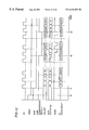
- FIG. 1 is a block diagram showing a schematic configuration of a memory device 1 having a flash memory.
- FIG. 2 s a memory map showing the correspondence between a medium sector address and an address of the flash memory in the first embodiment.
- FIG. 3 is a diagram relating to the description of the conversion of a medium sector address into a flash sector address and column address offset generation bits.
- FIG. 4 is a diagram showing the relation between a column address offset and the two lower bits of a medium sector address.
- FIG. 5 is a diagram showing the main flow of the processing of the memory device in the first embodiment.
- FIG. 6 is a flow chart representing in detail the read process of step S 04 shown in FIG. 5 .
- FIG. 7 is a diagram illustrating the relation between the steps of the read process shown in FIG. 6 and the respective blocks in the memory device in which the steps are performed.
- FIG. 8 is a flow chart illustrating in detail the write process in step S 05 shown in FIG. 5 .
- FIG. 9 is a diagram showing how each step of the write process shown in FIG. 8 is performed between a host system and a controller, and between the controller and a flash memory.
- FIG. 10 is a block diagram representing in detail a data transfer control portion 8 shown in FIG. 1 .
- FIG. 11 is a timing diagram showing the manner of data transfer from the flash memory to the buffer memory.
- FIG. 12 is an operation waveform chart illustrating in detail the data write operation to the buffer memory shown in FIG. 11 .
- FIG. 13 is a timing diagram showing the manner of data transfer from the buffer memory to the flash memory.
- FIG. 14 is an operation waveform chart relating to a more detailed description of the manner of data transfer from the buffer memory to the flash memory shown in FIG. 13 .
- FIG. 15 is a block diagram showing a schematic configuration of a memory device 51 of the second embodiment.
- FIG. 16 is a memory map showing the correspondence between a medium sector address and a flash memory address in the second embodiment.
- FIG. 17 is a diagram relating to the description of the conversion of a medium sector address into a flash memory sector address and a start column address.
- FIG. 18 is a diagram showing the relation between a start column address and the two lower bits of the medium sector address.
- FIG. 19 is a conceptual diagram relating to the description of a start column address.
- FIG. 20 is an operational waveform chart relating to the description of the command setting and the address setting when reading data from the flash memory having a partial read/program function.
- FIG. 21 is a diagram showing an input waveform when writing data into the flash memory in the second embodiment.
- FIG. 22 is a diagram showing the main flow of the processing of the memory device in the second embodiment.
- FIG. 23 is a flow chart representing in detail the read process of step S 104 shown in FIG. 22 .
- FIG. 24 is a diagram illustrating the relation between the steps of the read process shown in FIG. 23 and the respective blocks in the memory device in which the steps are performed.
- FIG. 25 is a flow chart illustrating in detail the write process in step S 105 shown in FIG. 22 .
- FIG. 26 is a diagram showing how each step of the write process shown in FIG. 25 is performed between a host system and a controller, and between the controller and a flash memory.
- FIG. 27 is a block diagram representing in detail a column address control portion 58 shown in FIG. 15 .
- FIG. 1 is a block diagram showing a schematic configuration of a memory device 1 having a flash memory.
- a memory device 1 for transmitting to and receiving from a host system 12 the external data to be stored.
- Memory device 1 includes a data input/output portion 9 for receiving a medium address from the host system to perform the address conversion and for performing the data conversion so as to allow the transmission and the reception of the external data between the memory device and the host system, and a flash memory 10 for performing the data transmission and reception according to an address signal converted by data input/output portion 9 .
- Data input/output portion 9 performs the data conversion from the data to be input into or output from flash memory 10 into the external data, and vice versa.
- Data input/output portion 9 includes a host interface portion 2 for performing the data transfer with the host system, a buffer memory 4 having a capacity of 512 bytes for temporarily storing a portion of sector data of a flash memory to allow host interface portion 2 to perform the data transfer with host system 12 , a flash interface portion 7 for controlling the data transmission and reception between buffer memory 4 and the flash memory according to a command from host interface portion 2 , and a flash memory 10 which is a semiconductor device for holding the data to be stored in memory device 1 .
- Flash interface portion 7 includes a sequencer portion 6 for sending, to the flash memory according to the specification of the flash memory, a command for setting the operation such as the read or write operation and an address for specifying a memory region during the read or write operation, and a data transfer control portion 8 for generating from a medium sector address provided from host system 12 a sector address and a column address offset of the flash memory.
- Flash memory 10 has a plurality of sectors, each of which having a capacity of 2084 bytes. When the sector address is specified, flash memory 10 can serially output 2048 bytes of data stored in the specified sector.
- FIG. 2 is a memory map showing the correspondence between a media sector address and an address of the flash memory in the first embodiment.
- Shown in FIG. 2 is the memory map in the case in which medium sector capacity, or a sector capacity which is a unit by which memory device 1 transmits and receives data at a time, is 512 bytes and the capacity of a sector of flash memory 10 is 2048 bytes. A one-fourth sector of flash memory 10 is assigned as a medium sector.
- a medium sector address 0h corresponds to flash memory column addresses 0h to 1FFh of a flash memory sector address 0h.
- a medium sector address 1h corresponds to flash memory column addresses 200h to 3FFh of flash memory sector address 0h.
- a medium sector address 2h corresponds to flash memory column addresses 400h to 5FFh of flash memory sector address 0h.
- a medium sector 3h corresponds to flash memory column addresses 600h to 7FFh of flash memory sector address 0h.
- FIG. 3 is a diagram relating to the description of the conversion of a medium sector address into a flash memory sector address and column address offset generation bits.
- the 14 higher bits MA 15 to MA 2 of a medium sector address are used as flash sector address bits SA 13 to SA 0 .
- MA 1 and MA 0 which are the two lower bits in a medium sector address are used as column address offset generation bits C 1 and C 0 , and a column address offset described below is generated from these column address offset generation bits.
- FIG. 4 is a diagram showing the relation between the column address offset and the two lower bits of the medium sector address.
- the column address offset is set to 0h, and the transmission and the reception of 512 bytes of data which is the medium sector capacity take place between the buffer memory and the flash memory.
- the column address offset is set to 200h, and the data transmission and reception take place between the buffer memory and the flash memory.
- the column address offset is set to 400h, and the data transmission and reception take place between the buffer memory and the flash memory.
- the column address offset is set to 600h, and the data transmission and reception take place between the buffer memory and the flash memory.
- FIG. 5 is a diagram showing the main flow of the processing of the memory device in the first embodiment.
- step S 01 the memory device waits for a request from the host system. Then step S 02 determines whether a read request has been made. If the read request has been made, the read process is performed in step S 04 . When the read process is complete, a return is made to step SO 1 and once again the memory device waits for a request from the host system.
- step S 03 determines whether a write request has been made by the host system. If the write request has been made, the write process is performed in step S 05 . When the write process is complete, a return is made to step S 01 and once again the memory device waits for a request from the host system.
- step S 03 If no write request has been made in step S 03 , a return is made to step S 01 , and once again the memory device waits for a request from the host system.
- FIG. 6 is a flow chart representing in detail the read process of step S 04 shown in FIG. 5 .
- the read process is started in step S 11 .
- step S 12 the memory device receives the medium sector address from the host system. Then, the address conversion is performed based on the medium sector address received, and the value of the column address offset shown in FIG. 4 is generated.
- step S 14 a sector read operation is performed from the flash memory.
- the data read out is written into the buffer memory based on the offset value in step S 15 .
- step S 16 an interrupt signal is sent to the host system, and in step S 17 the data written into the buffer memory is sent as read data to the host system.
- the read operation ends in step S 18 .
- FIG. 7 is a diagram illustrating the relation between the steps of the read process shown in FIG. 6 and the respective blocks in the memory device in which the steps are performed.
- controller refers to a portion including host interface portion 2 , flash interface sequencer portion 6 , and the buffer memory in FIG. 1 .
- a sector address SA and an offset value of the flash memory is generated from the medium sector address in the controller. Then, a read command and sector address SA are transmitted to the flash memory. As a consequence, the sector read operation is performed in the flash memory, and 2048 bytes of data is sent successively to the controller as a flash interface data output. Then the controller takes out the 512 bytes data corresponding to the offset based on the medium sector address and transfers the data to the buffer memory.
- the controller When the storing of data into the buffer memory is completed, the controller makes a read request for the data from the medium sector address, and the host system accepts an interrupt. Thereafter, the controller outputs data from the buffer memory, whereby the data read operation of the medium sector address is performed. Then the read operation is completed.
- FIG. 8 is a flow chart illustrating in detail the write process in step S 05 shown in FIG. 5 .
- the write operation starts in step S 21 .
- step S 22 the medium sector address transmitted from the host system is received by the memory device.
- step S 23 the memory device requests the host system to send data, and in step S 24 , the memory device receives the data from the host system. The data is written into the buffer memory in step S 25 .
- step S 26 an offset value is generated from the medium sector address received in step S 22 . Then, in step S 27 a program command for the flash memory is set. In step S 28 data from the buffer memory and the initial value data are combined, and the combined data is written into the flash memory at a prescribed timing.
- step S 29 The write operation ends in step S 29 .
- FIG. 9 is a diagram showing how each step of the write process shown in FIG. 8 is performed between the host system and the controller, and between the controller and the flash memory.
- a write request for the medium sector address is transmitted from the host system to the controller.
- the controller receives this request and makes a data write request for the medium sector address to the host system.
- the host system writes the data into the medium sector address.
- the data is input into the buffer memory via the controller.
- a sector address and an offset value of the flash memory are generated from the medium sector address which had been received.
- the program command and the sector address are transmitted to the flash memory.
- the flash memory is rendered data writable.
- the stored 512 byte data is transferred from the buffer memory based on the offset value.
- the time period other than the time period in which data stored in the buffer memory is transferred involves the transfer of write data “FFh.” After the write data including the buffer memory data is input into the flash memory, the write operation ends after a prescribed wait time.
- Each memory cell in the flash memory is formed by an MOS transistor having a floating gate.
- Each memory cell holds data “1” or “0” depending on the state of the threshold voltage of the MOS transistor.
- the state of the memory cell immediately after erasing the data of the memory cell corresponds to the held data “1.”
- the threshold voltage changes, and the state of the memory cell having the threshold voltage after the change corresponds to the held data “0.”
- the threshold voltages does not change. Therefore, even when data “1” is written into the memory cell which holds data “0” as the initial state, the held data does not change.
- FFh is written as the data without performing the erase operation in the first embodiment.
- FFh is one-byte data containing all “1” bits so that the flash memory retains the data it held before the write operation.
- FIG. 10 is a block diagram representing in detail a data transfer control portion 8 shown in FIG. 1 .
- data transfer control portion 8 includes a flip-flop 22 for latching in synchronism with the rise of a clock signal SC a read sector enable signal RSE# generated inside the memory device, an AND circuit 24 for outputting as a reset signal RST the logical sum of the output from flip-flop 22 and a write sector enable signal WSE# generated inside the memory device, an SC counter 26 which is reset by reset signal RST and thereafter starts the count-up in response to the rise of clock signal SC, a medium sector address latch portion 30 for latching a 16 bit medium sector address from the host system and for outputting the 14 higher bits as a sector address SA 0 to SA 15 to sequencer portion 6 , and a comparator 32 for comparing the 2 higher bits of the 11 bit count value of the output from SC counter 26 with the 2 lower bits of the medium sector address latched by medium sector address latch portion 30 .
- Comparator 32 outputs a comparison result signal CMP that attains a low or logic “L” level when the 2 bit data from SC counter 26 matches the 2 bit data from medium sector address latch portion 30 .
- Data transfer control portion 8 further includes a gate circuit 28 which receives the output from flip-flop 22 , clock signal SC, and result signal CMP and outputs a write enable signal /WE#, and a selector 34 which receives the output from buffer memory 4 and the fixed data “FFh” and outputs either of the received output from buffer memory 4 or “FFh” to the flash memory according to comparison result signal CMP.
- Selector 34 outputs to the flash memory the output from the buffer memory when comparison signal CMP is at a logic “L” level, and outputs fixed data “FFh” to the flash memory when comparison signal CMP is at a high or logic “H” level.
- buffer memory 4 is illustrated additionally in FIG. 10 .
- Buffer memory 4 receives the 9 lower bits of the 11 bit count value of SC counter 26 as an address signal ADR, write sector enable signal WSE# as an output enable signal /OE#, and the output of gate circuit 28 as write enable signal /WE#, and, in response to these signals, holds data input DI from the flash memory, or sends data output DO to the flash memory via selector 34 .
- FIG. 11 is a timing diagram showing the manner of data transfer the flash memory to the buffer memory.
- a data signal DATA is read from the flash memory according to clock signal SC from time T 1 . Since this read operation is performed sector by sector, normally 2048 bytes of data is read out continuously thereafter.
- the data read out from the flash memory is not transferred to the buffer memory between time t 1 and time t 2 .
- FIG. 12 is an operation waveform chart illustrating in detail the data write operation to the buffer memory shown in FIG. 11 .
- read sector enable signal RSE# falls from a logic “H” level to a logic “L” level with the read request being made from the host system.
- reset signal RST falls from the logic “H” level to the logic “L” level, and the reset of SC counter 26 is released.
- SC counter 26 counts up the 11 bit count value from 0h to 1FFh according to the input of clock signal SC.
- address signal ADR which is the 9 lower bits of the count value and is input into the buffer memory, changes from 0h to 1FFh.
- comparison result signal CMP is at the logic “H” level indicating a mismatch.
- comparison result signal CMP falls from the logic “H” level to the “L” level.
- Comparison result signal CMP maintains the logic “L” level while the count value is between 200h to 3FFh.
- gate circuit 28 outputs clock signal SC as write enable signal /WE# to the buffer memory. Since write enable signal /WE# is input into buffer memory 4 , the input data, data 0h to data 1FFh, are written into the address indicated by address signal ADR at the leading edge of write enable signal /WE#.
- comparison result signal CMP Since the count value of SC counter 26 is 400h or greater after time t 3 , comparison result signal CMP once again attains the logic “H” level, and data to be input thereafter is not written into the buffer memory.
- FIG. 13 is a timing diagram showing the manner of data transfer from the buffer memory to the flash memory.
- dummy data “FFh” is written into column addresses 0h to 1FFh of the flash memory from time t 1 to time t 2 .
- the dummy data is the data corresponding to the initial value held immediately after the flash memory is erased. In general, data held inside the flash memory is not destroyed by writing such initial value data into the flash memory.
- the memory device is most suitable for use including, for instance, the temporary storage of digital camera images, the storage of acoustic signals of portable digital audio equipment, and the like, where stored data is erased one unit at a time, and thereafter, new data is added in order into the unit that was erased.
- dummy data “FFh” is written as is the case between time t 1 and time t 2 .
- FIG. 14 is an operation waveform chart relating to a more detailed description of the manner of data transfer from the buffer memory to the flash memory shown in FIG. 13 .
- write sector enable signal WSE# falls from the logic “H” level to the “L” level in response to the write request from the host system. Accordingly, reset signal RST falls from the logic “H” level to the logic “L” level, and the reset of SC counter 26 is released. In addition, output enable input signal /OE# of the buffer memory falls from the “H” level to the “L” level, and buffer memory 4 becomes accessible.
- comparison result signal CMP falls from the logic “H” level to the “L” level according to the change in the count value.
- Data at the address specified by address signal ADR is read from buffer memory 4 , and is transferred to the flash memory as data output signal DO via selector 34 . From then on until time t 3 , the data transfer from the buffer memory to the flash memory takes place.
- comparison result signal CMP rises from the “L” level to the “H” level according to the change in the count value at time t 3 so that the data output signal once again attains fixed value “FFh” output by selector 34 when comparison result signal CMP is at the “H” level.
- the memory device is most suitable for use including, for instance, the temporary storage of digital camera images, the storage of acoustic signals of portable digital audio equipment, and the like, where data is erased one unit at a time, and thereafter, new data is added in order into the unit that was erased.
- medium sector capacity which is the capacity unit for data transfer with the host system
- capacity of a sector of the flash memory used the capacity of the buffer memory for the temporary storage of data can be made smaller according to the medium sector capacity so that a memory device having an advantage with respect to the cost can be provided in constructing the hardware.
- FIG. 15 is a block diagram showing a schematic configuration of a memory device 51 of the second embodiment.
- a memory device 51 for transmitting to and receiving from a host system 12 the external data to be stored.
- Memory device 51 includes a data input/output portion 59 for receiving a medium address from the host system to perform address conversion and for performing the data conversion so as to allow the transmission and the reception of the external data between the memory device and the host system, and a flash memory 60 for performing the data transmission and reception according to an address signal converted by data input/output portion 59 .
- Data input/output portion 59 performs the data conversion from the data to be input into or output from flash memory 60 into the external data, and vice versa.
- Data input/output portion 59 includes a host interface portion 52 for performing the data transfer with host system 12 , a buffer memory 54 having a capacity of 512 bytes for temporarily storing storage data to allow host interface portion 52 to perform the data transfer with host system 12 , and a flash interface portion 57 for controlling the data transmission and reception between buffer memory 54 and flash memory 60 according to a command from host interface portion 52 .
- Flash interface portion 57 includes a sequencer portion 56 for sending, to the flash memory according to the specification of the flash memory, a command for setting the operation such as the read or write operation and an address for specifying a memory region during the read or write operation, and a column address control portion 58 for generating from a medium sector address provided from host system 12 a sector address of the flash memory and a start column address for specifying the read start location of the column specified by the sector address.
- flash memory 60 has a partial read/program function in which the data read and write operations can be started from any column address of a sector.
- Flash memory 60 has a plurality of sectors, each of which having a capacity of 2048 bytes.
- sector address When the sector address is specified, flash memory 60 can serially output the data corresponding to the specified sector alone in synchronism with a clock signal. Further, when a start column address is specified, the data corresponding to the column address of the specified sector up to the data corresponding to the final address of the sector can be serially output in synchronism with a clock signal.
- FIG. 16 is a memory map showing the correspondence between a medium sector address and a flash memory address in the second embodiment.
- FIG. 17 is a diagram relating to the description of the conversion of a medium sector address into a flash memory sector address and a start column address.
- the 14 higher bits MA 15 to MA 2 of a medium sector address are used as bits of a flash sector address SA 13 to SA 0 .
- MA 1 and MA 0 which are two lower bits in a medium sector address are used as CA 10 and CA 9 , respectively, in the start column address.
- CA 11 and CA 8 to CAO are all set to “0h.”
- FIG. 18 is a diagram showing the relation between the start column address of the flash memory and the two lower bits of a medium sector address.
- the start column address is set to 0h, and when MA 1 and MA 0 are 0 and 1, respectively, the start column address is set to 200h.
- the start column address is set to 400h, and when MA 1 and MA 0 are both 1's, the start column address is set to 600h.
- the address conversion is performed in column address control portion 58 of FIG. 15, which is readily implemented by providing the wiring connection corresponding to FIG. 18 .
- FIG. 19 is a conceptual diagram relating to the description of a start column address.
- FIG. 20 is an operational waveform chart relating to the description of the command setting and the address setting when reading data from the flash memory having a partial read/program function.
- SA( 1 ) which is the 8 lower bits of the sector address is taken into the flash memory at the leading edge of write enable signal /WE#.
- SA( 2 ) which is the 6 higher bits of the sector address is taken into the flash memory at the leading edge of write enable signal /WE#.
- CA( 1 ) which is the 8 lower bits of start column address CA is taken into the flash memory at the leading edge of write enable signal /WE#.
- CA( 2 ) which is the 4 higher bits of the start column address is taken into the flash memory at the leading edge of write enable signal /WE#.
- FIG. 21 is a diagram showing an input waveform when writing data into the flash memory in the second embodiment.
- SA( 1 ) which is the 8 lower bits of the sector address is taken into the flash memory at the leading edge of write enable signal /WE#.
- SA( 2 ) which is the 6 higher bits of the sector address is taken into the flash memory at the leading edge of write enable signal /WE#.
- CA( 1 ) which is the 8 lower bits of the start column address is taken into the flash memory at the leading edge of write enable signal /WE#.
- CA( 2 ) which is the 4 higher bits of the start column address is taken into the flash memory at the leading edge of write enable signal /WE#.
- FIG. 22 is a diagram showing the main flow of the processing of the memory device in the second embodiment.
- the main flow of the processing of the memory device in the second embodiment differs from the flow shown in FIG. 5 in that read process step S 04 of the first embodiment shown in FIG. 5 is replaced by step S 104 , and that write process step S 05 is replaced by step S 105 .
- Other parts are identical to the flow shown in FIG. 5, and the description thereof will not be repeated.
- FIG. 23 is a flow chart representing in detail the read process of step S 104 shown in FIG. 22 .
- the read operation is started in step S 111 .
- step S 112 the memory device receives a medium sector address from the host system. Then, in step S 113 , the received medium sector address is converted into sector address SA and start column address CA of the flash memory. In step S 114 , a partial read command of the flash memory is set, and sector address SA and start column address CA are also specified. Then in step S 115 , data is read from the flash memory and written into the buffer memory.
- an interrupt signal is sent to the host system in step S 116 .
- step S 117 data written into the buffer memory is sent as read data to the host system.
- step S 118 the read operation is completed.
- FIG. 24 is a diagram illustrating the relation between the steps of the read process shown in FIG. 23 and the respective blocks in the memory device in which the steps are performed.
- controller refers to a portion including host interface portion 52 , flash interface sequencer portion 56 , and the buffer memory 54 in FIG. 15 .
- sector address SA and start column address CA of the flash memory are generated from the medium sector address in the controller. Then, the controller sends a read command, sector address SA and the start column address to the flash memory. Consequently, a partial read operation is performed in the flash memory, and 512 bytes of data is output to the buffer memory.
- the controller makes a read request for data from the specified medium sector address to the host system. The data is read from the buffer memory to the host system, and the read operation is completed.
- FIG. 25 is a flow chart illustrating in detail the write process in step S 105 shown in FIG. 22 .
- the write operation starts in step S 121 .
- step S 122 the medium sector address transmitted from the host system is received by the memory device.
- step S 123 the memory device requests the host system to send data, and receives the data from the host system in step S 124 .
- the data is written into the buffer memory in step S 125 .
- step S 126 sector address SA and start column address CA of the flash memory are generated from the medium sector address received in step S 122 . Then, in step S 127 a partial program command is set for the flash memory, and thereafter, sector address SA and start column address CA are specified.
- step S 128 the data is read from the buffer memory and is written into the flash memory. Then the data write operation ends in step S 129 .
- FIG. 26 is a diagram showing how each step of the write process shown in FIG. 25 is performed between the host system and the controller, and between the controller and the flash memory.
- a write request for the medium sector address is transmitted from the host system to the controller.
- the controller receives this request and makes a data write request for the medium sector address to the host system.
- the host system writes the data into the medium sector address.
- the data is input into the buffer memory via the controller.
- sector address SA and start column address CA of the flash memory are generated from the medium sector address which had been received.
- the controller sets the program command, sector address /SA and start column address /CA for the flash memory. Consequently, the flash memory performs a partial program operation.
- the 512 bytes of data is input from the buffer memory to the flash memory, and the data write operation is performed starting with a prescribed column address.
- the address control of the buffer memory and the generation of the address signal provided to the flash memory from the medium sector address take place in column address control portion 58 shown in FIG. 15 .
- FIG. 27 is a block diagram representing in detail a column address control portion 58 shown in FIG. 15 .
- column address control portion 58 includes a flip-flop 72 for latching in synchronism with the rise of a clock signal SC a read sector enable signal RSE# generated inside the memory device, an AND circuit 74 for outputting as a reset signal RST the logical sum of the output from flip-flop 72 and a write sector enable signal WSE# generated inside the memory device, a 9 bit SC counter 76 which is reset by reset signal RST and thereafter starts the count-up in response to the rise of clock signal SC, a medium sector address latch portion 80 for latching a 16 bit medium sector address from the host system and for outputting the 14 bits SA 0 to SA 13 of a sector address and 12 bits CA 0 to CA 11 of a start column address, to sequencer portion 6 , and a gate circuit 78 for receiving the output from flip-flop 72 and clock signal SC to output a write enable signal /WE#.
- buffer memory 54 is illustrated in FIG. 27 .
- Buffer memory 54 receives the 9 bits of the count value of SC counter 76 as an address signal ADR, write sector enable signal WSE# as an output enable signal /OE#, and the output of gate circuit 78 as write enable signal /WE#, and, in response to the these signals, receives and holds data input DI from the flash memory, or sends data output DO to the flash memory.
- the capacity of the buffer memory for the temporary storage of data during the data transfer between the host interface portion and the host system can be made smaller than the capacity of one sector of the flash memory so that a memory device having an advantage with respect to the cost can be provided.
- the provision and the use of a flash memory capable of performing the partial read/program allow the read and rewrite operations one medium sector as a unit.
Landscapes
- Engineering & Computer Science (AREA)
- Theoretical Computer Science (AREA)
- Physics & Mathematics (AREA)
- General Engineering & Computer Science (AREA)
- General Physics & Mathematics (AREA)
- Human Computer Interaction (AREA)
- Memory System (AREA)
- Read Only Memory (AREA)
Abstract
Description
Claims (13)
Applications Claiming Priority (2)
| Application Number | Priority Date | Filing Date | Title |
|---|---|---|---|
| JP11-098019 | 1999-04-05 | ||
| JP09801999A JP4141581B2 (en) | 1999-04-05 | 1999-04-05 | Storage device with flash memory |
Publications (2)
| Publication Number | Publication Date |
|---|---|
| US20020083262A1 US20020083262A1 (en) | 2002-06-27 |
| US6434658B1 true US6434658B1 (en) | 2002-08-13 |
Family
ID=14208160
Family Applications (1)
| Application Number | Title | Priority Date | Filing Date |
|---|---|---|---|
| US09/395,941 Expired - Fee Related US6434658B1 (en) | 1999-04-05 | 1999-09-14 | Memory device operable with a small-capacity buffer memory and having a flash memory |
Country Status (2)
| Country | Link |
|---|---|
| US (1) | US6434658B1 (en) |
| JP (1) | JP4141581B2 (en) |
Cited By (14)
| Publication number | Priority date | Publication date | Assignee | Title |
|---|---|---|---|---|
| US6684289B1 (en) * | 2000-11-22 | 2004-01-27 | Sandisk Corporation | Techniques for operating non-volatile memory systems with data sectors having different sizes than the sizes of the pages and/or blocks of the memory |
| US20050141273A1 (en) * | 2003-12-31 | 2005-06-30 | Min-Gun Park | Flash memory system capable of inputting/outputting sector data at random |
| US20060039196A1 (en) * | 2003-10-03 | 2006-02-23 | Gorobets Sergey A | Corrected data storage and handling methods |
| US20060136655A1 (en) * | 2004-12-16 | 2006-06-22 | Gorobets Sergey A | Cluster auto-alignment |
| US20060155922A1 (en) * | 2004-12-16 | 2006-07-13 | Gorobets Sergey A | Non-volatile memory and method with improved indexing for scratch pad and update blocks |
| US20060155920A1 (en) * | 2004-12-16 | 2006-07-13 | Smith Peter J | Non-volatile memory and method with multi-stream updating |
| US20060155921A1 (en) * | 2004-12-16 | 2006-07-13 | Gorobets Sergey A | Non-volatile memory and method with multi-stream update tracking |
| US20060161722A1 (en) * | 2004-12-16 | 2006-07-20 | Bennett Alan D | Scratch pad block |
| US7174348B1 (en) * | 2002-11-26 | 2007-02-06 | Unisys Corporation | Computer program having an object module and a software development tool integration module which automatically interlink artifacts generated in different phases of a software project |
| US20070086243A1 (en) * | 2005-10-18 | 2007-04-19 | Samsung Electronics Co., Ltd. | Nor-nand flash memory device with interleaved mat access |
| US20080098190A1 (en) * | 2002-04-05 | 2008-04-24 | Renesas Technology Corp. | Non-volatile storage device |
| US20080266988A1 (en) * | 2004-01-30 | 2008-10-30 | Samsung Electronics Co., Ltd. | Multi- port memory device for buffering between hosts and non-volatile memory devices |
| US20090031080A1 (en) * | 2007-07-25 | 2009-01-29 | Hynix Semiconductor Inc. | Flash memory device and program method thereof |
| US11074175B1 (en) * | 2013-01-28 | 2021-07-27 | Radian Memory Systems, Inc. | Flash memory controller which assigns address and sends assigned address to host in connection with data write requests for use in issuing later read requests for the data |
Families Citing this family (47)
| Publication number | Priority date | Publication date | Assignee | Title |
|---|---|---|---|---|
| JP4711531B2 (en) * | 2001-03-23 | 2011-06-29 | ルネサスエレクトロニクス株式会社 | Semiconductor memory device |
| JP4082913B2 (en) * | 2002-02-07 | 2008-04-30 | 株式会社ルネサステクノロジ | Memory system |
| US7406628B2 (en) * | 2003-07-15 | 2008-07-29 | Seagate Technology Llc | Simulated error injection system in target device for testing host system |
| US7600087B2 (en) * | 2004-01-15 | 2009-10-06 | Hitachi, Ltd. | Distributed remote copy system |
| JP2005285191A (en) * | 2004-03-29 | 2005-10-13 | Nec Electronics Corp | Nonvolatile semiconductor memory device and its driving method |
| JP4713867B2 (en) * | 2004-09-22 | 2011-06-29 | 株式会社東芝 | Memory controller, memory device, and memory controller control method |
| KR100666169B1 (en) * | 2004-12-17 | 2007-01-09 | 삼성전자주식회사 | Flash memory data storing device |
| KR100737913B1 (en) * | 2005-10-04 | 2007-07-10 | 삼성전자주식회사 | Read method of semiconductor memory device |
| US20070100893A1 (en) * | 2005-10-31 | 2007-05-03 | Sigmatel, Inc. | System and method for accessing data from a memory device |
| JP4661748B2 (en) * | 2006-09-22 | 2011-03-30 | Tdk株式会社 | MEMORY CONTROLLER, FLASH MEMORY SYSTEM HAVING MEMORY CONTROLLER, AND FLASH MEMORY CONTROL METHOD |
| JP2008112285A (en) * | 2006-10-30 | 2008-05-15 | Toshiba Corp | Non-volatile memory system |
| JP4498341B2 (en) * | 2006-11-20 | 2010-07-07 | 株式会社東芝 | Memory system |
| US9201790B2 (en) * | 2007-10-09 | 2015-12-01 | Seagate Technology Llc | System and method of matching data rates |
| US8959307B1 (en) | 2007-11-16 | 2015-02-17 | Bitmicro Networks, Inc. | Reduced latency memory read transactions in storage devices |
| US8665601B1 (en) | 2009-09-04 | 2014-03-04 | Bitmicro Networks, Inc. | Solid state drive with improved enclosure assembly |
| US9135190B1 (en) | 2009-09-04 | 2015-09-15 | Bitmicro Networks, Inc. | Multi-profile memory controller for computing devices |
| US8447908B2 (en) | 2009-09-07 | 2013-05-21 | Bitmicro Networks, Inc. | Multilevel memory bus system for solid-state mass storage |
| US8560804B2 (en) | 2009-09-14 | 2013-10-15 | Bitmicro Networks, Inc. | Reducing erase cycles in an electronic storage device that uses at least one erase-limited memory device |
| US9372755B1 (en) | 2011-10-05 | 2016-06-21 | Bitmicro Networks, Inc. | Adaptive power cycle sequences for data recovery |
| US9043669B1 (en) | 2012-05-18 | 2015-05-26 | Bitmicro Networks, Inc. | Distributed ECC engine for storage media |
| KR20140082173A (en) * | 2012-12-24 | 2014-07-02 | 에스케이하이닉스 주식회사 | Address Counting Circuit and Semiconductor Apparatus Using the same |
| US9423457B2 (en) | 2013-03-14 | 2016-08-23 | Bitmicro Networks, Inc. | Self-test solution for delay locked loops |
| US9916213B1 (en) | 2013-03-15 | 2018-03-13 | Bitmicro Networks, Inc. | Bus arbitration with routing and failover mechanism |
| US9971524B1 (en) | 2013-03-15 | 2018-05-15 | Bitmicro Networks, Inc. | Scatter-gather approach for parallel data transfer in a mass storage system |
| US9720603B1 (en) | 2013-03-15 | 2017-08-01 | Bitmicro Networks, Inc. | IOC to IOC distributed caching architecture |
| US9430386B2 (en) | 2013-03-15 | 2016-08-30 | Bitmicro Networks, Inc. | Multi-leveled cache management in a hybrid storage system |
| US9798688B1 (en) | 2013-03-15 | 2017-10-24 | Bitmicro Networks, Inc. | Bus arbitration with routing and failover mechanism |
| US10120694B2 (en) | 2013-03-15 | 2018-11-06 | Bitmicro Networks, Inc. | Embedded system boot from a storage device |
| US9501436B1 (en) | 2013-03-15 | 2016-11-22 | Bitmicro Networks, Inc. | Multi-level message passing descriptor |
| US9672178B1 (en) | 2013-03-15 | 2017-06-06 | Bitmicro Networks, Inc. | Bit-mapped DMA transfer with dependency table configured to monitor status so that a processor is not rendered as a bottleneck in a system |
| US9934045B1 (en) | 2013-03-15 | 2018-04-03 | Bitmicro Networks, Inc. | Embedded system boot from a storage device |
| US9400617B2 (en) | 2013-03-15 | 2016-07-26 | Bitmicro Networks, Inc. | Hardware-assisted DMA transfer with dependency table configured to permit-in parallel-data drain from cache without processor intervention when filled or drained |
| US10489318B1 (en) | 2013-03-15 | 2019-11-26 | Bitmicro Networks, Inc. | Scatter-gather approach for parallel data transfer in a mass storage system |
| US9842024B1 (en) | 2013-03-15 | 2017-12-12 | Bitmicro Networks, Inc. | Flash electronic disk with RAID controller |
| US9875205B1 (en) | 2013-03-15 | 2018-01-23 | Bitmicro Networks, Inc. | Network of memory systems |
| US9734067B1 (en) | 2013-03-15 | 2017-08-15 | Bitmicro Networks, Inc. | Write buffering |
| US10078604B1 (en) | 2014-04-17 | 2018-09-18 | Bitmicro Networks, Inc. | Interrupt coalescing |
| US10025736B1 (en) | 2014-04-17 | 2018-07-17 | Bitmicro Networks, Inc. | Exchange message protocol message transmission between two devices |
| US10042792B1 (en) | 2014-04-17 | 2018-08-07 | Bitmicro Networks, Inc. | Method for transferring and receiving frames across PCI express bus for SSD device |
| US9952991B1 (en) | 2014-04-17 | 2018-04-24 | Bitmicro Networks, Inc. | Systematic method on queuing of descriptors for multiple flash intelligent DMA engine operation |
| US10055150B1 (en) | 2014-04-17 | 2018-08-21 | Bitmicro Networks, Inc. | Writing volatile scattered memory metadata to flash device |
| US9811461B1 (en) | 2014-04-17 | 2017-11-07 | Bitmicro Networks, Inc. | Data storage system |
| US10552050B1 (en) | 2017-04-07 | 2020-02-04 | Bitmicro Llc | Multi-dimensional computer storage system |
| FR3065303B1 (en) * | 2017-04-12 | 2019-06-07 | Stmicroelectronics (Rousset) Sas | WRITING METHOD IN A NON-VOLATILE MEMORY DEVICE AND CORRESPONDING NON-VOLATILE MEMORY DEVICE |
| US11030148B2 (en) * | 2018-04-04 | 2021-06-08 | Lawrence Livermore National Security, Llc | Massively parallel hierarchical control system and method |
| JP2022074450A (en) * | 2020-11-04 | 2022-05-18 | キオクシア株式会社 | Memory card, memory system, and file fragmentation resolving method |
| KR20220060372A (en) * | 2020-11-04 | 2022-05-11 | 에스케이하이닉스 주식회사 | Memory system and operating method thereof |
Citations (6)
| Publication number | Priority date | Publication date | Assignee | Title |
|---|---|---|---|---|
| US5627783A (en) * | 1995-01-31 | 1997-05-06 | Mitsubishi Denki Kabushiki Kaisha | Semiconductor disk device |
| US5724285A (en) * | 1996-03-08 | 1998-03-03 | Mitsubishi Denki Kabushiki Kaisha | Flash memory PC card capable of refreshing data a predetermined time after the PC card is removed from a host |
| US5765002A (en) * | 1995-03-13 | 1998-06-09 | Intel Corporation | Method and apparatus for minimizing power consumption in a microprocessor controlled storage device |
| JPH10207726A (en) | 1997-01-23 | 1998-08-07 | Oki Electric Ind Co Ltd | Semiconductor disk device |
| US5905993A (en) * | 1994-11-09 | 1999-05-18 | Mitsubishi Denki Kabushiki Kaisha | Flash memory card with block memory address arrangement |
| US5963474A (en) * | 1998-05-11 | 1999-10-05 | Fujitsu Limited | Secondary storage device using nonvolatile semiconductor memory |
-
1999
- 1999-04-05 JP JP09801999A patent/JP4141581B2/en not_active Expired - Fee Related
- 1999-09-14 US US09/395,941 patent/US6434658B1/en not_active Expired - Fee Related
Patent Citations (6)
| Publication number | Priority date | Publication date | Assignee | Title |
|---|---|---|---|---|
| US5905993A (en) * | 1994-11-09 | 1999-05-18 | Mitsubishi Denki Kabushiki Kaisha | Flash memory card with block memory address arrangement |
| US5627783A (en) * | 1995-01-31 | 1997-05-06 | Mitsubishi Denki Kabushiki Kaisha | Semiconductor disk device |
| US5765002A (en) * | 1995-03-13 | 1998-06-09 | Intel Corporation | Method and apparatus for minimizing power consumption in a microprocessor controlled storage device |
| US5724285A (en) * | 1996-03-08 | 1998-03-03 | Mitsubishi Denki Kabushiki Kaisha | Flash memory PC card capable of refreshing data a predetermined time after the PC card is removed from a host |
| JPH10207726A (en) | 1997-01-23 | 1998-08-07 | Oki Electric Ind Co Ltd | Semiconductor disk device |
| US5963474A (en) * | 1998-05-11 | 1999-10-05 | Fujitsu Limited | Secondary storage device using nonvolatile semiconductor memory |
Cited By (28)
| Publication number | Priority date | Publication date | Assignee | Title |
|---|---|---|---|---|
| US7032065B2 (en) * | 2000-11-22 | 2006-04-18 | Sandisk Corporation | Techniques for operating non-volatile memory systems with data sectors having different sizes than the sizes of the pages and/or blocks of the memory |
| US6684289B1 (en) * | 2000-11-22 | 2004-01-27 | Sandisk Corporation | Techniques for operating non-volatile memory systems with data sectors having different sizes than the sizes of the pages and/or blocks of the memory |
| US7171513B2 (en) | 2000-11-22 | 2007-01-30 | Sandisk Corporation | Techniques for operating non-volatile memory systems with data sectors having different sizes than the sizes of the pages and/or blocks of the memory |
| US7581058B2 (en) * | 2002-04-05 | 2009-08-25 | Renesas Technology Corp. | Non-volatile memory having multiple erase operations |
| US20080098190A1 (en) * | 2002-04-05 | 2008-04-24 | Renesas Technology Corp. | Non-volatile storage device |
| US7174348B1 (en) * | 2002-11-26 | 2007-02-06 | Unisys Corporation | Computer program having an object module and a software development tool integration module which automatically interlink artifacts generated in different phases of a software project |
| US7173852B2 (en) | 2003-10-03 | 2007-02-06 | Sandisk Corporation | Corrected data storage and handling methods |
| US20060039196A1 (en) * | 2003-10-03 | 2006-02-23 | Gorobets Sergey A | Corrected data storage and handling methods |
| US20050141273A1 (en) * | 2003-12-31 | 2005-06-30 | Min-Gun Park | Flash memory system capable of inputting/outputting sector data at random |
| US7782683B2 (en) * | 2004-01-30 | 2010-08-24 | Samsung Electronics Co., Ltd. | Multi-port memory device for buffering between hosts and non-volatile memory devices |
| US20080266988A1 (en) * | 2004-01-30 | 2008-10-30 | Samsung Electronics Co., Ltd. | Multi- port memory device for buffering between hosts and non-volatile memory devices |
| US20060155921A1 (en) * | 2004-12-16 | 2006-07-13 | Gorobets Sergey A | Non-volatile memory and method with multi-stream update tracking |
| US20080301359A1 (en) * | 2004-12-16 | 2008-12-04 | Peter John Smith | Non-Volatile Memory and Method With Multi-Stream Updating |
| US7315916B2 (en) | 2004-12-16 | 2008-01-01 | Sandisk Corporation | Scratch pad block |
| US20060161722A1 (en) * | 2004-12-16 | 2006-07-20 | Bennett Alan D | Scratch pad block |
| US7366826B2 (en) | 2004-12-16 | 2008-04-29 | Sandisk Corporation | Non-volatile memory and method with multi-stream update tracking |
| US7386655B2 (en) | 2004-12-16 | 2008-06-10 | Sandisk Corporation | Non-volatile memory and method with improved indexing for scratch pad and update blocks |
| US7395404B2 (en) | 2004-12-16 | 2008-07-01 | Sandisk Corporation | Cluster auto-alignment for storing addressable data packets in a non-volatile memory array |
| US7412560B2 (en) | 2004-12-16 | 2008-08-12 | Sandisk Corporation | Non-volatile memory and method with multi-stream updating |
| US20060155920A1 (en) * | 2004-12-16 | 2006-07-13 | Smith Peter J | Non-volatile memory and method with multi-stream updating |
| US8151035B2 (en) | 2004-12-16 | 2012-04-03 | Sandisk Technologies Inc. | Non-volatile memory and method with multi-stream updating |
| US20060136655A1 (en) * | 2004-12-16 | 2006-06-22 | Gorobets Sergey A | Cluster auto-alignment |
| US20060155922A1 (en) * | 2004-12-16 | 2006-07-13 | Gorobets Sergey A | Non-volatile memory and method with improved indexing for scratch pad and update blocks |
| US7532521B2 (en) | 2005-10-18 | 2009-05-12 | Samsung Electronics Co., Ltd. | NOR-NAND flash memory device with interleaved mat access |
| US20070086243A1 (en) * | 2005-10-18 | 2007-04-19 | Samsung Electronics Co., Ltd. | Nor-nand flash memory device with interleaved mat access |
| US20090031080A1 (en) * | 2007-07-25 | 2009-01-29 | Hynix Semiconductor Inc. | Flash memory device and program method thereof |
| US8296499B2 (en) * | 2007-07-25 | 2012-10-23 | Hynix Semiconductor Inc. | Flash memory device and program method thereof |
| US11074175B1 (en) * | 2013-01-28 | 2021-07-27 | Radian Memory Systems, Inc. | Flash memory controller which assigns address and sends assigned address to host in connection with data write requests for use in issuing later read requests for the data |
Also Published As
| Publication number | Publication date |
|---|---|
| JP4141581B2 (en) | 2008-08-27 |
| US20020083262A1 (en) | 2002-06-27 |
| JP2000293427A (en) | 2000-10-20 |
Similar Documents
| Publication | Publication Date | Title |
|---|---|---|
| US6434658B1 (en) | Memory device operable with a small-capacity buffer memory and having a flash memory | |
| USRE50067E1 (en) | Storage device including flash memory and capable of predicting storage device performance based on performance parameters | |
| US6525952B2 (en) | Recording system, data recording apparatus, memory apparatus, and data recording method | |
| US5548741A (en) | IC memory card system having a host processor selectively operable with an IC memory card including either an SRAM or an EEPROM | |
| EP0712067B1 (en) | Flash disk card | |
| US7039781B2 (en) | Flash memory apparatus and method for merging stored data items | |
| KR102641521B1 (en) | Key-value storage device and operating method thereof | |
| US6477632B1 (en) | Storage device and accessing method | |
| US8127072B2 (en) | Data storage device and method for accessing flash memory | |
| JPH08263361A (en) | Flash memory card | |
| JP4874588B2 (en) | Storage device and host device | |
| JP4034971B2 (en) | Memory controller and memory system device | |
| US20090248981A1 (en) | Semiconductor storage device | |
| JP2006039966A (en) | Memory card, card controller installed in memory card, and processing unit of memory card | |
| JP2001243110A (en) | Memory controller, flash memory system and access method to flash memory | |
| US5724544A (en) | IC memory card utilizing dual eeproms for image and management data | |
| US20070047308A1 (en) | Memory controller, flash memory system and control method for flash memory | |
| US7606993B2 (en) | Flash memory controller, memory control circuit, flash memory system, and method for controlling data exchange between host computer and flash memory | |
| CN114328297A (en) | Mapping table management method, memory control circuit unit and memory storage device | |
| TWI793993B (en) | Memory system and memory control method | |
| KR100538338B1 (en) | Method for Uniformly Distributing Memory Blocks of Flash Memory and Data Storage Device Using The Method | |
| JP2005250619A (en) | Nonvolatile storage device and its rewriting method | |
| JP4731584B2 (en) | Storage device with flash memory | |
| JP4018085B2 (en) | Nonvolatile memory, memory card using the same, information processing apparatus, and software write protection control method for nonvolatile memory | |
| JP2003178280A (en) | Memory card |
Legal Events
| Date | Code | Title | Description |
|---|---|---|---|
| AS | Assignment |
Owner name: MITSUBISHI DENKI KABUSHIKI KAISHA, JAPAN Free format text: ASSIGNMENT OF ASSIGNORS INTEREST;ASSIGNOR:FUKUZUMI, TOMOYA;REEL/FRAME:010248/0031 Effective date: 19990903 |
|
| FEPP | Fee payment procedure |
Free format text: PAYOR NUMBER ASSIGNED (ORIGINAL EVENT CODE: ASPN); ENTITY STATUS OF PATENT OWNER: LARGE ENTITY |
|
| FPAY | Fee payment |
Year of fee payment: 4 |
|
| FPAY | Fee payment |
Year of fee payment: 8 |
|
| AS | Assignment |
Owner name: RENESAS TECHNOLOGY CORP.,JAPAN Free format text: ASSIGNMENT OF ASSIGNORS INTEREST;ASSIGNOR:MITSUBISHI DENKI KABUSHIKI KAISHA;REEL/FRAME:024066/0781 Effective date: 20100304 |
|
| AS | Assignment |
Owner name: RENESAS ELECTRONICS CORPORATION, JAPAN Free format text: ASSIGNMENT OF ASSIGNORS INTEREST;ASSIGNOR:MITSUBISHI DENKI KABUSHIKI KAISHA;REEL/FRAME:025980/0219 Effective date: 20110307 |
|
| REMI | Maintenance fee reminder mailed | ||
| LAPS | Lapse for failure to pay maintenance fees | ||
| STCH | Information on status: patent discontinuation |
Free format text: PATENT EXPIRED DUE TO NONPAYMENT OF MAINTENANCE FEES UNDER 37 CFR 1.362 |
|
| FP | Lapsed due to failure to pay maintenance fee |
Effective date: 20140813 |