EP0488141A2 - Organisches elektrolumineszentes Element und leuchtemittierende Vorrichtung mit diesem Element - Google Patents
Organisches elektrolumineszentes Element und leuchtemittierende Vorrichtung mit diesem Element Download PDFInfo
- Publication number
- EP0488141A2 EP0488141A2 EP91120110A EP91120110A EP0488141A2 EP 0488141 A2 EP0488141 A2 EP 0488141A2 EP 91120110 A EP91120110 A EP 91120110A EP 91120110 A EP91120110 A EP 91120110A EP 0488141 A2 EP0488141 A2 EP 0488141A2
- Authority
- EP
- European Patent Office
- Prior art keywords
- time
- less
- light emitting
- organic
- light emission
- Prior art date
- Legal status (The legal status is an assumption and is not a legal conclusion. Google has not performed a legal analysis and makes no representation as to the accuracy of the status listed.)
- Granted
Links
Images


Classifications
-
- H—ELECTRICITY
- H05—ELECTRIC TECHNIQUES NOT OTHERWISE PROVIDED FOR
- H05B—ELECTRIC HEATING; ELECTRIC LIGHT SOURCES NOT OTHERWISE PROVIDED FOR; CIRCUIT ARRANGEMENTS FOR ELECTRIC LIGHT SOURCES, IN GENERAL
- H05B33/00—Electroluminescent light sources
-
- H—ELECTRICITY
- H05—ELECTRIC TECHNIQUES NOT OTHERWISE PROVIDED FOR
- H05B—ELECTRIC HEATING; ELECTRIC LIGHT SOURCES NOT OTHERWISE PROVIDED FOR; CIRCUIT ARRANGEMENTS FOR ELECTRIC LIGHT SOURCES, IN GENERAL
- H05B33/00—Electroluminescent light sources
- H05B33/12—Light sources with substantially two-dimensional radiating surfaces
- H05B33/14—Light sources with substantially two-dimensional radiating surfaces characterised by the chemical or physical composition or the arrangement of the electroluminescent material, or by the simultaneous addition of the electroluminescent material in or onto the light source
Definitions
- This invention relates to an organic electroluminescence element and a light emitting device employing the electroluminescence element.
- An organic electroluminescence element or an organic EL element is an element having a light emitting layer formed of an organic molecular or organic macromolecular material exhibiting electroluminescent properties. It has ideal properties as a display element such as viewability from a wide viewing angle because of autogenous light emission and superior shock proofness because it is a fully solid-state element. For this reason, researches and development are progressing in a number of technological fields.
- the organic EL element cannot be said to be satisfactory in response speed which is slower than the response speed of a light emitting diode of which response speed is an order of severaltens of nanoseconds.
- the organic EL element cannot be used such as a light emitting diode conventionally employed as a light emitting and transmitting element in a photocoupler or a photointerrupter.
- the EL element can not be used as a light emitting element for light communication for the similar reason.
- an object of the present invention to provide an organic EL element having a faster response speed and a light emitting device employing the EL element.
- the present inventors have conducted eager researches, and ultimately found that analyses of an equivalent circuit is of critical importance, i.e. that the analyses of the equivalent circuit has not been done and hence only the element with longer time constants have been obtained, which accounted for the low response speed of the conventional organic EL elements of the order of several microseconds.
- the present inventors have first found that the value of the time constant (RC time constant) ⁇ of the element is related with the capacitance C and the area of the element such that (i) it is necessary for the value of the time constant ⁇ of the element to be 100 nanoseconds or less to produce a fast response of the element shorter than 1 microsecond, a fast response rate being obtainable with the value of the time constant ⁇ of the element of 100 nanosecond or less; (ii) that the value of the time constant ⁇ of the element of 100 nanosecond or less may be obtained with the capacitance C of the element of 500 PF or less, i.e.
- C ⁇ 500 PF is equivalent to ⁇ ⁇ 100 ns; (iii) the value of the capacitance C of the element of 500 PF may be obtained with the area of the light-emitting surface of the element of 0.025 cm2 or less; and that (iv) if particularly necessary, the value of the time constant ⁇ of the element may be diminished to 10 nanosecond (ns) or less.
- the time constant of the element is 100 nanoseconds or less and/or the capacitance of the element is 500 PF or less and the charge transport time is 600 nanoseconds or less, whilst the area of the light emitting surface of the element is 0.025 cm2 or less and the charge transport time is 600 nanoseconds or less.
- the time constant of the resulting series connection is set so as to be 100 nanoseconds or less and/or the sum of the capacitances of the elements is 500 PF or less and the charge transport time of each element is set so as to be 600 nanoseconds or less.
- the time constant ⁇ of the element is set so as to be 10 nanoseconds or less.
- the time constant of the element is 10 nanoseconds or less and the hole transport time and the charge transport time are both 40 nanoseconds or less whilst the full rise time and the full decay time of light emission are both 50 nanoseconds or less.
- the light emitting device of the present invention is constituted by the above described organic EL element and a driving circuit in which the time constant as measured actually on driving the element is not in excess of 100 nanoseconds, if particularly necessary, is 10 nanoseconds or lower.
- a photocoupler of the present invention employs the above described organic EL element as a light emitting element for light transmission.
- a light emitting device for light communication includes a modulatable power source connected to the above described organic EL element of the present invention.
- an organic EL device with a fast response speed may be obtaind.
- the organic EL element or the light emitting device of the present invention may be utilized as a photocoupler, a photointerrupter or as a light emitting device for light communication.
- Fig. 1 shows an equivalent circuit of an organic EL element.
- Fig. 2 is a perspective view showing an example of an organic EL element of the present invention.
- Fig. 3 is an explanatory view showing a light emitting mechanism of an organic EL element.
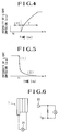
- Fig. 4 is a graph showing the rise of light emission in an organic EL element.
- Fig. 5 is a graph showing the decay of light emission in an organic EL element.
- Fig. 6 is a schematic circuit diagram of a photocoupler of the present invention.
- Fig. 7 is a front view showing an organic EL element of the present invention, as formed on a PIN diode.
- Fig. 8a is a plan view of an organic EL element prepared in accordance with Examples of the present invention
- Fig. 8b is a front view thereof.
- Fig. 9 is a schematic circuit diagram showing a light emitting device prepared in accordance with Examples of the present invention.
- Fig. 10 is a graph showing the rise in light emission of the light emitting device prepared in accordance with the Examples.
- Fig. 11 is a graph showing the decay in light emission of the light emitting device prepared in accordance with the Examples.
- Fig. 12 is a graph showing a light emission waveform in Comparative Examples.
- Fig. 13 is a graph showing an impressed voltage waveform and a light emission waveform of another organic EL element prepared in accordance with the Examples.
- the time constant of the element is selected to be 100 nanoseconds or less.
- the time constant of the element is explained with reference to an equivalent circuit thereof.
- 1 is an organic EL element constituted by stacking a glass substrate 2, an ITO electrode (anode) 3, a hole injection layer 4, a light emitting layer 5 and a cathode (Mg; Ag) 6, step by step, as shown in Fig. 2.
- C is a capacitance of the element which, with an area S and a film thickness d of the element, is expressed by the formula (1) (see Fig. 2), where ⁇ o is the permittivity (dielectric constant) in vacuum and ⁇ r is the relative permittivity of an organic layer.
- the value of the capacitance C which depends on the film thickness of the organic layer, is 40 to 10 nF/cm2 for the total film thickness 60 to 260 nm of a light emitting layer and a charge transport layer (hole injection layer) used as an organic layer summed together.
- the capacitance value is proportional to the area of the element.
- R1 is a resistance connected in parallel with capacitance C and composed of resistances in the charge transport layer and the light emitting layer of the element and a resistance at an interface between an electrode and the organic layer (the charge transport layer or the light emitting layer).
- the resistance R1 becomes smaller with increase in the applied voltage and in typically approximately equal to several tens to 100 ohm per cm2 when a forward voltage V of 5 to 10 V is applied to the element. This resistance of the element is inversely proportionate to the area of the element surface.
- R2 is a resistance connected in series with the capacitance C and is composed of a resistance of the electrode and a wiring resistance of the element.
- the resistance R2 is usually 1 to 100 ohms.
- V is a power source driving the element.
- the time constant ⁇ is related with C, R1 and R2 as shown in the formula (2) above, so that, if the values of C and R2 are reduced, the value of the time constant ⁇ becomes smaller. Since the capacitance C is proportional to the area S of the element surface, the value of the time constant ⁇ becomes smaller with reduction in the area S of the element surface. On the other hand, since the resistance R2 is mainly composed of the wiring resistance and is not related closely with the area of the element surface so that its effect on the time constant ⁇ is relatively small.
- the film thickness d of the element in the formula (1) or the relative permittivity ⁇ r may also be changed for reducing the capacitance C.
- the area of the surface of the conventional organic EL element is 0.2 cm2 or more.
- the capacitance C may be set so as to be not larger than 500 PF (C ⁇ 500 PF). Since R1 » R2, ⁇ CR2 ⁇ 100 ns, from the formula (2), so as to provide a basis for the preparation of the element having fast response characteristics.
- the value of ⁇ CR2 (for R1 » R2) may be calculated from the values of C and R2.
- the value of the time constant ⁇ of the element preferably CR2 ⁇ 50 ns and more preferable CR2 ⁇ 10 ns.
- the corresponding value of the capacitance C is preferably not more than 500 PF and more preferably not more than 200 PF.
- the film thickness of the organic layer of 130 nm is not more than 0.01 cm2.
- the film thickness of 300 nm or more is not desirable because the light emitting efficiency of the element is reduced and the element driving voltage is not more than 20 V.
- the film thickness and the capacitance of the element be 300 nm or less and 200 PF or less, respectively.
- wiring connection is preferably so made that, except the resistance of the electrode portion taking charge of the light emission of the element (portion 3 of ITO electrode in Fig. 2), the resistance be not more than several ohms.
- the time constant of the series connection be not more than 100 ns and/or the sum total of the capacitances of the element be not more than 500 PF.
- the elements are preferable connected together so that the voltage be applied in the forward direction.
- the time constant of the element be selected to be 10 nanoseconds or less.
- the actual value of the time constant ⁇ becomes larger than the theoretical value on account of the inner resistance in the power source or the wiring resistance with the elements. It is therefore necessary that the EL element be driven by a driving circuit for which the actual time constant is 100 ns or less, preferably 10 ns or less, as will be explained subsequently.
- the light emitting response behavior of the element is not determined solely by the time constant ⁇ and that the charge transport involved in the charge injection, a transfer and recombination process is necessary until start of light emission, while the rise time is necessary until a stabilized steady state of light emission is established.
- the light emitting mechanism of the organic EL element is hereinafter explained.
- a transparent electrode 203 (anode) is supported on a substrate 201.
- a hole transport region 205 is disposed on the anode 203, and an electrone transport region 207 is disposed on the transport region 205 in tight contact with a cathode 209.
- the hole transport region 205 holes are transported to a recombination region where the holes are recombined with the electrons to produce an excited state of the molecules of a light emitting material.
- the region 205 includes a portion of a hole injection layer or a light emitting layer.
- the electron transport region 207 electrons are transported to the recombination region.
- the rigion 207 includes a portion of an electron implanting layer or the light emitting layer.
- a positive (+) voltage and a negative (-) voltage are applied, after lapse a time ⁇ , to the anode 203 the cathode 209, respectively.
- the holes are injected from the anode 203 into the hole transport region 205.
- the holes 210 are transported, under an electrical field generated by the impressed voltage, in the direction of the electron transport region 207 through the hole transport region 205. If the electron transport region 207 includes the light emitting layer, the light emitting layer exists in a portion within the electron transport region 207 which is in intimate contact with the hole transport region 205. The holes transported in this portion is injected into the light emitting layer from the hole transport region 205.
- electrons 211 are injected from the cathode 209 into the electron transport region 207 and transported under the electrical field through the electron transport region 207 before reaching the light emitting layer.
- the electrons and the holes are responsible for the excited state of the molecules of the light emitting material, and light is emitted on reversion to the ground state.
- the transport time of charges i.e. electrons and holes, is necessary for starting light emission in the element, besides the time ⁇ necessary for an electrical voltage to be impressed substantially on the element.
- the time T during which the charges are moved through a region of 60 nm under the strength of the electrical field of 1 ⁇ 106 V/cm is 600 ns for the mobility of 1 ⁇ 10 ⁇ 5 cm2/v ⁇ sec. Therefore, in order for the rise in light emission to be completed in 1 microsecond or less, a mobility not less than 1 ⁇ 10 ⁇ 5 cm2/v ⁇ sec is preferably needed for a region having a film thickness of 60 nm. For achieving a rise complete time for light emission of not longer than 1 microsecond for an arbitrary film thickness, the film thickness and mobility are set so that the transport time is not longer than 600 ns.
- the mobility of the holes is 10 ⁇ 3 to 10 ⁇ 4 cm2/v ⁇ sec.
- the mobility ⁇ h of ⁇ h > 2 ⁇ 10 ⁇ 4 cm2/v ⁇ sec may be achieved easily if the hole injection layer or the light emitting layer is formed of any of these materials.
- Th ⁇ 40 ns may be achieved for the strength of the electrical field of not lower than 1 MV/cm.
- the charge transport time T is determined in a majority of cases by the electron mobility of a material employed for the electron transport region.
- the mobility is preferably of an order of 10 ⁇ 5 cm2/v ⁇ sec or more and more preferably 8 ⁇ 10 ⁇ 5 cm2/v ⁇ sec or more.
- the charge transport time T may be diminished to satisfy Te ⁇ 50 ns.
- a material with the mobility ⁇ e of 10 ⁇ 3 to 10 ⁇ 4 cm2/v ⁇ sec may be found in future with the progress in the researches into the materials for the electron transport region. The information of the present invention may be utilized fully for such case.
- the rise time is necessitated until a stable steady state of light emission is reached.
- the rise complete time ⁇ + T + T' is of an order of 1 microsecond or more for ⁇ > 100 ns
- the rise complete time ⁇ + T + T' is substantially shorter than 500 ns under the condition of ⁇ ⁇ 20 ns, as shown in Table 1. If T and T' are not dependent on the time constant ⁇ , the rise complete time ⁇ + T + T' is changed by a variance (80 ns) of ⁇ so that the rise complete time can not be changed by as much as 500 ns or more.
- the capacitance of the element be preferably set so that ⁇ ⁇ 20 ns or, occasionally, ⁇ ⁇ 10 ms.
- Fig. 5 shows the state of rising of light emission when the capacitance of the element is set so that ⁇ ⁇ 20 ns. If the power source is turned off at time t1 in Fig. 5, decay occurs acutely as indicated at I.
- the area I represents an area of an exponential relaxation in which decay occurs at a rate corresponding to the life of fluorescence of molecules comprising the light emitting layer.
- the time involved for this area is usually 50 ns or less.
- the time corresponds to the time of relaxation from the excited state generated before t1 to the ground state, and represents a fast decay of light emission.
- the area (I) in Fig. 5 is governed by the life of fluorescence, as discussed above. Therefore, the shorter the life of fluorescence, the faster is the decay of light emission.
- the life of fluorescence is preferably not longer than 100 ns and more preferably not longer than 20 ns.
- An area (II) is an area of prolonged relaxation resulting from recombination of holes and electrons left in the light emitting layer.
- a constant characterizing this area is a recombination constant, which is a rate constant for the rate of recombination of the electrons and the holes producing the excited state.
- a time of a rise completion for light emission which is necessary to reach 90% of the steady state light emission is less than 300 ns.
- the light emission rise complete time may be 50 ns or shorter. Since relaxation is governed only by the life of fluorescence if the long life relaxation component may be disregarded, the light emission decay complete time may be set so as to be not more than 50 ns for a shorter life of fluorescence, for which the response frequency is 20 MHz.
- the organic EL element of the present invention is preferably formed on a substrate.
- a substrate There is no particular limitation to the starting materials for the substrate and any of the materials conventionally used for the organic EL elements, such as glass, transparent plastics or quartz, may be employed.
- the substrate thickness is preferably 10 times or more that of the organic EL element.
- transparent electrode materials such as metals, e.g. gold, aluminum, indium, magnesium, copper or silver, alloys or mixtures thereof, alloys or mixtures disclosed in JP Patent KOKAI Publication No. 63-299695(1988), ITO (indium tin oxide; a mixed oxide of indium oxide and tin oxide), Sn O2 (stannic oxide)or ZnO (zinc oxide), may be employed.
- metals e.g. gold, aluminum, indium, magnesium, copper or silver, alloys or mixtures thereof, alloys or mixtures disclosed in JP Patent KOKAI Publication No. 63-299695(1988)
- ITO indium tin oxide; a mixed oxide of indium oxide and tin oxide
- Sn O2 stannic oxide
- ZnO zinc oxide
- Metals or electrically conductive compounds having a higher work function are preferably employed for an anode, whilst metals or electrically conductive materials having a lower work function are preferably employed for a cathode.
- At least one of the electrodes is preferably transparent or semi-transparent for raising the light transmittivity.
- the electrode thickness is preferably 10 nm to 1 ⁇ m and, above all, not more than 200 nm, for raising the transmittivity.
- the electrodes may be formed in any known manner, such as by vapor deposition or sputtering.
- the organic layer including at least a light emitting layer formed of organic compound, may consist only of a light emitting layer, a light emitting layer/a hole injection layer, an electron transport layer/light emitting layer, or of an electron transport layer/light emitting layer/a hole injection layer, or in any other manner as described in JP Patent Application No. 1-068387(1989).
- the organic layer includes a sole layer. The sequence of the component layers of the organic layer may be reversed.
- the light emitting layer has injection, transporting and light emitting functions.
- the injection function means the function of enabling holes to be injected by the anode or the hole injection layer on application of an electrical field, and the function of enabling electrons to be injected by the cathode or the electron injection layer.
- the transporting function means the function of moving or transporting holes and electrons under the force of an electrical field.
- the light emitting function means the function of providing a site for recombination of holes and electrons and of causing light emission.
- the capability of hole injection may differ from that of electron injection.
- the light emitting layer is preferably in the range of from 5 nm to 5 ⁇ m.
- the hole injection layer and the electron injection layer are preferably provided for improving the light emitting properties.
- the hole injection layer is formed of a material capable of transporting holes to the light emitting layer under a lower electrical field.
- the mobility of holes is preferably at least 10 ⁇ 6 cm2/v ⁇ sec under the electrical field of 104 to 106 v/cm.
- the electron injecting layer is formed of a material capable of transporting electrons to the light emitting layer under a lower electrical field.
- the method for vapor deposition is preferred because the organic EL element may thereby be prepared in one process with advantages in equipment and production time.
- the above described organic EL element may be prepared by ageing by impressing a voltage across the anode and the cathode.
- the ageing herein means applying an electrical voltage to eliminate a region liable to produce leakage currents as well as to remove holes or electrons accumulated in the element (see JP Patent Application No. 2-117885). In this manner, the organic EL element may be operated stable.
- the organic EL element employed in the method of the present invention need not necessarily be processed by ageing. However, ageing is preferred for the sake of stabilizing the element operation.
- the light emitting device of the present invention will be hereinafter explained.
- the light emitting device of the present invention is adapted to be driven by a driving circuit (power source) which is so designed that the time constant during driving of the element is not in excess of 100 ns and occasionally 10 ns.
- a driving circuit power source
- the driving circuit is preferably so designed that a short pulse voltage may be applied during rise time and decay time.
- the above described organic EL element and light emitting device of the present invention may be used as a light emitting transmitting element and a light emitting transmitting device in a photocoupler or a photointerrupter which is in need of frequency response characteristics of 20 MHz (max. 50 MHz). That is, if the organic EL element 1 of the present invention is driven by a pulse power source 21 shown in Fig. 6 to produce the light emitting, interrupting or demodulating state, a pulse train is regenerated by a light receiving element 22 facing the power source.
- electrical-electrical conversion device may be provided by making a light emitting portion of the organic EL element of fast response characteristic and by making a light receiving portion of a light emitting element such as existing silicon photodiode, silicon PIN photodiode, avalanche photodiode or photomultiplier.
- an organic EL element on a substrate of a light receiving element, formed of a semiconductor, such as a silicon photodiode, an integrated circuit of a photocoupler or a photointerrupter may be easily provided.
- Fig. 7 shows an example of such integrated circuit of a photocoupler in which the organic EL element 1 is formed on a PIN photodiode 31.
- the PIN photodiode 31 is composed of an N-layer 32, an I-layer 33 and a P-layer 34.
- An SiO2 window material 35 is deposited on the P-layer 34, and the organic EL element, similar to that shown in Fig. 2, is formed on the window material 35.
- the organic EL element of the present invention may be utilized as a light emitting device for light communication if the EL element is connected to a modulatable power source, in which case the light emitting and receiving devices are connected together by an optical fiber cable.
- a high speed light receiving element such as PIN photodiode
- a high speed organic EL element is combined with a high speed organic EL element, and changes of voltage wich are caused by the light modulation incident on the light receiving element are applied across the organic EL element, high speed light-light conversion may also be achieved.
- ITO In2 O3; Sn
- a Mo evaporation boat contained TPD (N,N'-diphenyl-N,N'-di(3-methylphenyl)-4,4'-diaminobiphenyl) and a Mo evaporation boat contained Al(O x )3 (Al complex of 8-hydroxyquinoline) were mounted on a terminal block adapted for current conduction and a vacuum chamber was evacuated to 10 ⁇ 6 Torr.
- Current conducted through a TPD boat for vacuum deposition of TPD to produce a layered assembly of the glass substrate/ITO/PPD.
- the rate of TPD deposition was 1 to 3 ⁇ /sec, the film thickness was 60 nm and the substrate temperature was the ambient temperature.
- the TPD deposition rate at this time was 1 to 2 ⁇ /sec, the film thickness was 60 nm and the substrate temperature was the ambient temperature.
- the vacuum chamber was them opened and a stainless steel mask was placed on the resulting glass substrate/ITO/TPD/Al(Ox)3 assembly.
- the resulting assembly was then mounted on the substrate holder.
- the mask area was 0.5mm2 (1 ⁇ 0.5) to provide a light emission area of the element.
- a Mo boat contained Mg and a W filament contained in were fitted on a terminal block for current conduction and the vacuum chamber was evacuated to a vacuum of 6 ⁇ 10 ⁇ 7 Torr.
- Current was supplied through the Mg-containing boat for vacuum deposition of Mg at a deposition rate of 14 ⁇ /sec.
- Current was simultaneously supplied to the In-containing boat for depositing In at a rate of 0.6 to 0.9 ⁇ /sec.
- Mg; In was formed to a thickness of 90 nm, while Mg; In was used as a cathode.
- the produced element is shown in a plan view of Fig. 8a and a cross-sectional view of Fig. 8b.
- a region H delimited by an Mg; In 6 and an ITO 3 represents a light-emitting region of the element.
- the capacitance of the element was found to be 100 PF.
- R1 was not known, R2 was found to be 25 ohms.
- the time constant ⁇ was estimated to be 2.5 ns.
- R1 was not known, R1 » R2 because of the small element area.
- a pulse generator 41 capable of applying a pulse voltage providing a rise time of and a decay time of approximately 20 ns each, was used in association with a circuit shown in Fig. 9.
- An oscilloscope 42 with a high bandwidth was also connected as shown in Fig. 9.
- the oscilloscope has an equivalent resistance of 50 ohms as indicated in a dotted line.
- the inner resistance 43 of the power source was 50 ohms.
- the waveform of light emission from the organic EL element was measured with a high-speed oscilloscope 45, having an enclosed terminal resistance of 50 ohms, using a photoelectron multiplier 44 (R 928 prepared by HAMAMATSU PHOTONICS KK) as a light receiver adapted for measuring high-speed response characteristics.
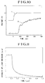
- Fig. 10 shows a voltage waveform I (voltage, 10 V) applied across the EL element, as measured with the oscilloscope 42.
- the waveform of the applied voltage rises acutely, demonstrating that the time constant of the element is less than 20 ns.
- the corresponding waveform of the light emission II indicates that the time until the light emission is initiated is equal to ⁇ + T ⁇ 70 ns.
- the value of the time constant ⁇ may be measured by measuring the time when the voltage after time ⁇ is equal to the value shown by the formula (6) above.
- the above given value of ⁇ was measured by this method. It should however be remarked that the measured value of the time constant includes the rise time of the pulse generator in addition to the time constant of the element, and the rise time of the pulse generator is not considered in the above formula (5).
- Fig, 11 shows the light emission decay behavior after the power source is turned off.
- the light emission shows exponential decay until about 40 ns, after which it shows long-time type light emission decay as determined by a recombination constant.
- the time until light emission decays to about 90 % of the equilibrium state was approximately 300 ns.
- Example 2 An element was prepared in the same manner as in Example 1, except that the area of the element surface by which the element emits light was 2 ⁇ 5 mm. The capacitance of the element was 2,000 PF. Measurements were made of the element in the similar manner as in Example 2 to give a light emission waveform as shown in Fig. 12, where t o and t2 indicate the waveform when the power source is turned on and off, respectively. From the results of these measurements, it was found that the time until the light emission starts to rise is 550 ns, whilst the time until the waveform of light emission reaches 90% of the equilibrium state was 2.2 ⁇ s. The time until the light emission decayed to 90 % of the equilibrium state was 700 ns.
- Organic EL elements were prepared in the same manner as in Example 1, and the light emission devices were prepared in the same manner as in Example 2, except changing the element area as shown in Table 1.
- the rise time ⁇ + T + T' and decay time T'' of light emission are strongly related with the surface area, that is the capacitance and hence the time constant of the element, such that, the smaller is the capacitance of the element, the higher is its rate of response.
- the capacitance of the element is preferably 500 PF or less and more preferably 200 PF or less, for which the response rate is 500 ns or less.
- a pulse train having the frequency of 3 MHz was prepared by a pulse generator of Example 1. This pulse generator was set as shown in Fig. 9 of the Example 2, and the pulse train was applied to the organic EL element for light emission with the pulses. The light emission was received by a S 1190 PIN photodiode produced by HAMAMATSU PHOTONICS KK, as a result of which a pulse train having a frequency of 3 MHz was reproduced. A 50 ohm terminal resistance was annexed to the PIN photodiode and the potential across its ends was measured. This Example illustrates that the electrical-electrical conversion (light communication) may proceed expeditiously.
- a function generator was connected to the element of Example 1 and sinusoidal modulation was performed to measure the light emission response.
- the light emission for the frequency of 4.6 MHz was 0.707 times the light emission power for the frequency of 3 MHz (3).
- Example 6 A test similar to that of Example 6 was conducted on the element of Comparative Example 1. The frequency for which the response was 0.707 times the light emission power for the frequency of +20 KHz was only 140 KHz.
- the Mo evaporation boat was attached to a current conducting terminal block of a vacuum deposition chamber, and a vacuum chamber was evacuated to 1.5 ⁇ 10 ⁇ 4 Pa.
- the BC Z VB containing boat was heated for vacuum deposition of BC Z VB at a vacuum deposition rate of 1 to 3 ⁇ /sec and a film thickness of 60 nm to produce an assembly having a layered structure of glass substrate/ITO/BC Z VB.
- the substrate temperature was ambient temperature.
- the vacuum tank was opened and, with a stainless steel mask applied to the BC Z VB layer, the substrate was attached to the substrate holder.
- the mask was previously prepared so that the light emission area of the element was 1 mm ⁇ 0.5 mm.
- a Mo boat containing Mg and a W filament containing Ag were mounted on the conducting terminal block, and the vacuum chamber was evacuated to 1 ⁇ 10 ⁇ 4 Pa.
- the current was conducted to the Mg-containing boat and concurrent dual vacuum deposition was effected at Mg a vacuum deposition rate of 18 to 20 ⁇ /sec and at an Ag vacuum deposition rate of 0.6 to 0.8 ⁇ /sec for forming a Mg; Ag layer to a film thickness of 1300 ⁇ . This layer was used as a Mg; Ag cathode.
- the response time of light emission of the produced element was measured in the same manner in Example 2, except using a pulse generator AVR-E2-C-P-W-03, produced by ABTEC Inc., capable of providing a rise and decay of the pulse voltage of approximately 1 ns each.
- a photoelectron multiplier RL5640-01, prepared by HAMAMATSU PHOTONICS KK was employed, which exhibited a high-speed response and which was capable of faithfully reproducing the light emission of the EL element.
- Fig. 13 shows an applied voltage waveform as measured with an oscilloscope, and EL signals as a waveform of the light emission response.
- the applied voltage waveform rises sharply indicating that the time constant of the element is 5 to 6 ns, (In Fig. 10, it may be presumed that the rise of the applied waveform becomes dull due to the time constant of the element).
- the corresponding waveform of the light emission shows ⁇ + T ⁇ 6 ns.
- the time until the light emission waveform reaches 90 % of the equilibrium state, or the light emission rise complete time ⁇ + T + T', is 24 ns, thus indicating an extremely high speed.
- the time until the light emission waveform decays to 90 % of the equilibrium state of light emission, or the light emission decay complete time was as short as 14 ns, thus similarly indicating an extremely high speed.
- the light emitting layer (9BC Z VB layer) of the present element is excellent in hole transportation and is estimated to correspond to the thickness dh and the thickness de approximately equal to 60 nm and 0 to 5 nm, respectively. It is therefore presumed that the recombination zone existed in contiguity to the cathode and the holes reach the recombination zone at an extremely high speed of 6 ns or less, where they are recombined with injected electrons. The amount of the long-life component, as the residual light component, was so small and there existed only a fluorescent light component having a short decay complete time of light emission.
- a glass substrate/ITO/BC Z VB assembly was prepared in the same manner as in Example 7.
- a boat containing Al(Ox)3 charged in advance into a separate Mo boat was heated to produce a 12 nm electron injection layer.
- the rate of deposition was 1 to 3 ⁇ /sec, and the substrate temperature was the ambient temperature.
- the vacuum tank was evacuated to 1 ⁇ 10 ⁇ 4 Pa and an Mg; Ag cathode was prepared as in Example 7.
- the produced element was evaluated in the same manner as in Example 7 except using the pulse voltage of 33 V.
- the RC time constant was 8 ns or less, the light emission rise complete time was 18 ns and the light emission decay complete time was 14 ns, thus indicating an extremely high speed. It is noted that separately conducted measurement of the light emission spectrum revealed that the spectrum of the element of Example 7 coincided with that of the element of Example 8 so that the BC Z VB layer was identified as a light emitting layer. Ultra high speed response could be realized since a portion within the BC Z VB layer facing the Al(Ox)3 layer is a recombination zone, and also since both the hole transport time in the BC Z VB layer and the electron transport time in the Al(Ox)3 layer are 14 ns or less.
Landscapes
- Electroluminescent Light Sources (AREA)
Applications Claiming Priority (4)
| Application Number | Priority Date | Filing Date | Title |
|---|---|---|---|
| JP32322990 | 1990-11-28 | ||
| JP323229/90 | 1990-11-28 | ||
| JP216244/91 | 1991-08-02 | ||
| JP3216244A JP2780880B2 (ja) | 1990-11-28 | 1991-08-02 | 有機エレクトロルミネッセンス素子および該素子を用いた発光装置 |
Publications (3)
| Publication Number | Publication Date |
|---|---|
| EP0488141A2 true EP0488141A2 (de) | 1992-06-03 |
| EP0488141A3 EP0488141A3 (en) | 1993-02-17 |
| EP0488141B1 EP0488141B1 (de) | 1998-03-04 |
Family
ID=26521320
Family Applications (1)
| Application Number | Title | Priority Date | Filing Date |
|---|---|---|---|
| EP91120110A Expired - Lifetime EP0488141B1 (de) | 1990-11-28 | 1991-11-26 | Organisches elektrolumineszentes Element und leuchtemittierende Vorrichtung mit diesem Element |
Country Status (4)
| Country | Link |
|---|---|
| US (1) | US5216331A (de) |
| EP (1) | EP0488141B1 (de) |
| JP (1) | JP2780880B2 (de) |
| DE (1) | DE69129005T2 (de) |
Cited By (4)
| Publication number | Priority date | Publication date | Assignee | Title |
|---|---|---|---|---|
| GB2350926A (en) * | 1999-05-27 | 2000-12-13 | Seiko Epson Corp | Monolithic,semiconductor light emitting and receiving device |
| DE102006040788A1 (de) * | 2006-08-31 | 2008-03-27 | Fraunhofer-Gesellschaft zur Förderung der angewandten Forschung e.V. | Integrierter Optokoppler mit organischem Lichtemitter und anorganischem Photodetektor |
| EP1944349A1 (de) * | 2007-01-11 | 2008-07-16 | Fujikura, Ltd. | Organisches Elektrolumineszenz- und optisches Verbindungsmodul |
| EP1555856A3 (de) * | 1996-03-12 | 2010-09-22 | Idemitsu Kosan Company Limited | Organisches elektrolumineszentes Element und organische elektrolumineszente Anzeigevorrichtung |
Families Citing this family (75)
| Publication number | Priority date | Publication date | Assignee | Title |
|---|---|---|---|---|
| JP2846571B2 (ja) * | 1994-02-25 | 1999-01-13 | 出光興産株式会社 | 有機エレクトロルミネッセンス素子 |
| US6548956B2 (en) | 1994-12-13 | 2003-04-15 | The Trustees Of Princeton University | Transparent contacts for organic devices |
| US5707745A (en) | 1994-12-13 | 1998-01-13 | The Trustees Of Princeton University | Multicolor organic light emitting devices |
| US5703436A (en) | 1994-12-13 | 1997-12-30 | The Trustees Of Princeton University | Transparent contacts for organic devices |
| US6358631B1 (en) | 1994-12-13 | 2002-03-19 | The Trustees Of Princeton University | Mixed vapor deposited films for electroluminescent devices |
| JP3401356B2 (ja) * | 1995-02-21 | 2003-04-28 | パイオニア株式会社 | 有機エレクトロルミネッセンスディスプレイパネルとその製造方法 |
| JPH08330070A (ja) * | 1995-05-29 | 1996-12-13 | Pioneer Electron Corp | 発光素子の駆動法 |
| JPH10199674A (ja) * | 1996-11-15 | 1998-07-31 | Sanyo Electric Co Ltd | 有機エレクトロルミネッセンス素子の駆動方法、有機エレクトロルミネッセンス装置及び表示装置 |
| US5757139A (en) * | 1997-02-03 | 1998-05-26 | The Trustees Of Princeton University | Driving circuit for stacked organic light emitting devices |
| JPH1140365A (ja) * | 1997-07-16 | 1999-02-12 | Tdk Corp | 有機el素子およびその製造方法 |
| EP1394870B2 (de) * | 1997-10-09 | 2018-10-17 | The Trustees Of Princeton University | Phosphoreszente organische lichtemittierende Vorrichtung |
| US6157138A (en) * | 1998-12-31 | 2000-12-05 | Telefonaktiebolaget Lm Ericsson | Apparatus for illuminating an electroluminescent lamp that preserves battery power |
| JP2000352952A (ja) * | 1999-04-05 | 2000-12-19 | Canon Inc | 画像形成装置 |
| TW536836B (en) * | 2000-05-22 | 2003-06-11 | Semiconductor Energy Lab | Light emitting device and electrical appliance |
| US7339317B2 (en) | 2000-06-05 | 2008-03-04 | Semiconductor Energy Laboratory Co., Ltd. | Light-emitting device having triplet and singlet compound in light-emitting layers |
| US6905784B2 (en) | 2000-08-22 | 2005-06-14 | Semiconductor Energy Laboratory Co., Ltd. | Light emitting device |
| US6864628B2 (en) * | 2000-08-28 | 2005-03-08 | Semiconductor Energy Laboratory Co., Ltd. | Light emitting device comprising light-emitting layer having triplet compound and light-emitting layer having singlet compound |
| JP3560150B2 (ja) | 2000-09-14 | 2004-09-02 | 日本精機株式会社 | 有機el素子 |
| JP2002151271A (ja) * | 2000-11-15 | 2002-05-24 | Pioneer Electronic Corp | 有機el素子及びその製造方法 |
| JP4703887B2 (ja) * | 2001-04-27 | 2011-06-15 | 株式会社半導体エネルギー研究所 | 画像表示装置 |
| GB0130411D0 (en) * | 2001-12-20 | 2002-02-06 | Koninkl Philips Electronics Nv | Active matrix electroluminescent display device |
| US6888557B2 (en) * | 2002-03-15 | 2005-05-03 | Denso Corporation | Electroluminescent device with sufficient luminous power and driving method thereof |
| US20050195318A1 (en) * | 2003-02-07 | 2005-09-08 | Takahiro Komatsu | Organic information reading unit and information reading device using the same |
| JP4096877B2 (ja) * | 2003-02-07 | 2008-06-04 | 松下電器産業株式会社 | 情報読み取り素子及びそれを用いた情報読み取り装置 |
| JP2005032793A (ja) * | 2003-07-08 | 2005-02-03 | Matsushita Electric Ind Co Ltd | 有機光電変換素子 |
| JP2005032852A (ja) * | 2003-07-09 | 2005-02-03 | Matsushita Electric Ind Co Ltd | 有機光電変換素子 |
| WO2005096403A2 (en) * | 2004-03-31 | 2005-10-13 | Matsushita Electric Industrial Co., Ltd. | Organic photoelectric conversion element utilizing an inorganic buffer layer placed between an electrode and the active material |
| WO2006098505A1 (en) | 2005-03-16 | 2006-09-21 | Fujifilm Corporation | Platinum complex compound and organic electroluminescent device |
| JP2009176762A (ja) * | 2007-01-11 | 2009-08-06 | Fujikura Ltd | 有機エレクトロルミネッセンス素子及び光配線モジュール |
| US20080246394A1 (en) * | 2007-04-03 | 2008-10-09 | Fujikura Ltd. | Organic light-emitting diode element and optical interconnection module |
| JP2008271317A (ja) * | 2007-04-23 | 2008-11-06 | Sumitomo Chemical Co Ltd | 照明光通信システムおよび照明光通信用の送信装置 |
| JP5484690B2 (ja) | 2007-05-18 | 2014-05-07 | ユー・ディー・シー アイルランド リミテッド | 有機電界発光素子 |
| JP2009004753A (ja) | 2007-05-18 | 2009-01-08 | Fujifilm Corp | 有機電界発光素子 |
| JP4995137B2 (ja) | 2007-06-11 | 2012-08-08 | 富士フイルム株式会社 | ガスバリアフィルムおよびこれを用いた有機デバイス |
| JP2009076865A (ja) | 2007-08-29 | 2009-04-09 | Fujifilm Corp | 有機電界発光素子 |
| KR101548382B1 (ko) | 2007-09-14 | 2015-08-28 | 유디씨 아일랜드 리미티드 | 유기 전계 발광 소자 |
| US8586189B2 (en) | 2007-09-19 | 2013-11-19 | Fujifilm Corporation | Gas-barrier film and organic device comprising same |
| JP5438941B2 (ja) | 2007-09-25 | 2014-03-12 | ユー・ディー・シー アイルランド リミテッド | 有機電界発光素子 |
| JP5489446B2 (ja) | 2007-11-15 | 2014-05-14 | 富士フイルム株式会社 | 薄膜電界効果型トランジスタおよびそれを用いた表示装置 |
| JP5489445B2 (ja) | 2007-11-15 | 2014-05-14 | 富士フイルム株式会社 | 薄膜電界効果型トランジスタおよびそれを用いた表示装置 |
| JP5438955B2 (ja) | 2007-12-14 | 2014-03-12 | ユー・ディー・シー アイルランド リミテッド | 白金錯体化合物及びこれを用いた有機電界発光素子 |
| JP5243972B2 (ja) | 2008-02-28 | 2013-07-24 | ユー・ディー・シー アイルランド リミテッド | 有機電界発光素子 |
| JP4555358B2 (ja) | 2008-03-24 | 2010-09-29 | 富士フイルム株式会社 | 薄膜電界効果型トランジスタおよび表示装置 |
| JP4531836B2 (ja) | 2008-04-22 | 2010-08-25 | 富士フイルム株式会社 | 有機電界発光素子並びに新規な白金錯体化合物及びその配位子となり得る新規化合物 |
| JP5117422B2 (ja) | 2008-07-15 | 2013-01-16 | 富士フイルム株式会社 | 発光装置及びその製造方法 |
| JP5117326B2 (ja) | 2008-08-29 | 2013-01-16 | 富士フイルム株式会社 | カラー表示装置及びその製造方法 |
| JP2010102968A (ja) * | 2008-10-23 | 2010-05-06 | Sumitomo Chemical Co Ltd | 照明光通信システム用の送信装置 |
| JP2010102969A (ja) * | 2008-10-23 | 2010-05-06 | Sumitomo Chemical Co Ltd | 照明光通信システム用の送信装置 |
| JP2010102967A (ja) * | 2008-10-23 | 2010-05-06 | Sumitomo Chemical Co Ltd | 照明光通信システム用の送信装置 |
| JP5314380B2 (ja) * | 2008-10-23 | 2013-10-16 | 住友化学株式会社 | 照明光通信システム用の送信装置 |
| JP2010102966A (ja) * | 2008-10-23 | 2010-05-06 | Sumitomo Chemical Co Ltd | 照明光通信システム用の送信装置 |
| JP2010153820A (ja) | 2008-11-21 | 2010-07-08 | Fujifilm Corp | 有機電界発光素子 |
| JP2010182449A (ja) | 2009-02-03 | 2010-08-19 | Fujifilm Corp | 有機el表示装置 |
| JP2010186723A (ja) | 2009-02-13 | 2010-08-26 | Fujifilm Corp | 有機el装置及びその製造方法 |
| JP2010205650A (ja) | 2009-03-05 | 2010-09-16 | Fujifilm Corp | 有機el表示装置 |
| JP5650889B2 (ja) | 2009-03-26 | 2015-01-07 | ユー・ディー・シー アイルランド リミテッド | 無機材料、デバイス及び有機電界発光素子 |
| WO2010110347A1 (ja) | 2009-03-27 | 2010-09-30 | 富士フイルム株式会社 | 有機電界発光素子及び有機電界発光素子の製造方法 |
| WO2010110280A1 (ja) | 2009-03-27 | 2010-09-30 | 富士フイルム株式会社 | 有機電界発光素子用塗布液 |
| JP2010254962A (ja) | 2009-03-30 | 2010-11-11 | Fujifilm Corp | 導電性ポリマー組成物、導電性硬化膜、及び、有機電界発光素子 |
| EP3389110B1 (de) | 2009-07-31 | 2023-12-27 | UDC Ireland Limited | Organisches elektrolumineszentes element |
| JP5779318B2 (ja) | 2009-08-31 | 2015-09-16 | ユー・ディー・シー アイルランド リミテッド | 有機電界発光素子 |
| JP2011060549A (ja) | 2009-09-09 | 2011-03-24 | Fujifilm Corp | 有機el装置用光学部材及び有機el装置 |
| JP2011202129A (ja) | 2010-03-26 | 2011-10-13 | Fujifilm Corp | ポリエステル樹脂、並びに、これを用いた光学材料、フィルムおよび画像表示装置 |
| JP5032684B1 (ja) * | 2011-05-27 | 2012-09-26 | 株式会社東芝 | 発光装置、表示装置、及び有機電界発光素子の駆動方法 |
| JP2013093541A (ja) | 2011-10-06 | 2013-05-16 | Udc Ireland Ltd | 有機電界発光素子とそれに用いることができる化合物および有機電界発光素子用材料、並びに該素子を用いた発光装置、表示装置及び照明装置 |
| JP2013084732A (ja) | 2011-10-07 | 2013-05-09 | Udc Ireland Ltd | 有機電界発光素子及び該素子用発光材料並びに発光装置、表示装置及び照明装置 |
| JP2013118349A (ja) | 2011-11-02 | 2013-06-13 | Udc Ireland Ltd | 有機電界発光素子、有機電界発光素子用材料並びに該有機電界発光素子を用いた発光装置、表示装置及び照明装置 |
| JP2013103918A (ja) | 2011-11-15 | 2013-05-30 | Udc Ireland Ltd | 電荷輸送材料、有機電界発光素子及び該素子を用いたことを特徴とする発光装置、表示装置または照明装置 |
| JP5981770B2 (ja) | 2012-01-23 | 2016-08-31 | ユー・ディー・シー アイルランド リミテッド | 有機電界発光素子、有機電界発光素子用電荷輸送材料、並びに、該素子を用いた発光装置、表示装置及び照明装置 |
| JP6118034B2 (ja) | 2012-02-06 | 2017-04-19 | ユー・ディー・シー アイルランド リミテッド | 有機電界発光素子とそれに用いることができる化合物および有機電界発光素子用材料、並びに該素子を用いた発光装置、表示装置及び照明装置 |
| US9136496B2 (en) * | 2013-01-08 | 2015-09-15 | Joled Inc. | Organic el device |
| CN111454297A (zh) | 2014-05-08 | 2020-07-28 | 环球展览公司 | 稳定的咪唑并菲啶材料 |
| JP6538339B2 (ja) * | 2014-12-12 | 2019-07-03 | 株式会社Joled | 有機el素子および有機el素子の製造方法 |
| KR102584846B1 (ko) | 2015-05-05 | 2023-10-04 | 유니버셜 디스플레이 코포레이션 | 유기 전계발광 재료 및 디바이스 |
| EP3492480B1 (de) | 2017-11-29 | 2021-10-20 | Universal Display Corporation | Organische elektrolumineszente materialien und vorrichtungen |
Family Cites Families (6)
| Publication number | Priority date | Publication date | Assignee | Title |
|---|---|---|---|---|
| US3673572A (en) * | 1969-11-24 | 1972-06-27 | Xerox Corp | Electroluminescent device |
| US3710181A (en) * | 1970-09-22 | 1973-01-09 | Matsushita Electric Industrial Co Ltd | Solid-state image intensifier |
| US3753231A (en) * | 1971-10-04 | 1973-08-14 | Secr Defence | Electroluminescent devices |
| JPH086087B2 (ja) * | 1988-02-09 | 1996-01-24 | 信越化学工業株式会社 | 電界発光素子 |
| EP0349265A3 (de) * | 1988-06-27 | 1990-03-14 | EASTMAN KODAK COMPANY (a New Jersey corporation) | Elektrolumineszente Vorrichtungen |
| CA2005289A1 (en) * | 1988-12-14 | 1990-06-14 | Chishio Hosokawa | Electroluminescence device |
-
1991
- 1991-08-02 JP JP3216244A patent/JP2780880B2/ja not_active Expired - Fee Related
- 1991-11-26 EP EP91120110A patent/EP0488141B1/de not_active Expired - Lifetime
- 1991-11-26 DE DE69129005T patent/DE69129005T2/de not_active Expired - Lifetime
- 1991-11-27 US US07/799,201 patent/US5216331A/en not_active Expired - Lifetime
Cited By (6)
| Publication number | Priority date | Publication date | Assignee | Title |
|---|---|---|---|---|
| EP1555856A3 (de) * | 1996-03-12 | 2010-09-22 | Idemitsu Kosan Company Limited | Organisches elektrolumineszentes Element und organische elektrolumineszente Anzeigevorrichtung |
| GB2350926A (en) * | 1999-05-27 | 2000-12-13 | Seiko Epson Corp | Monolithic,semiconductor light emitting and receiving device |
| DE102006040788A1 (de) * | 2006-08-31 | 2008-03-27 | Fraunhofer-Gesellschaft zur Förderung der angewandten Forschung e.V. | Integrierter Optokoppler mit organischem Lichtemitter und anorganischem Photodetektor |
| US7626207B2 (en) | 2006-08-31 | 2009-12-01 | Fraunhofer-Gesellschaft Zur Foerderung Der Angewandten Forschung E.V. | Integrated optocoupler with organic light emitter and inorganic photodetector |
| DE102006040788B4 (de) * | 2006-08-31 | 2013-02-07 | Fraunhofer-Gesellschaft zur Förderung der angewandten Forschung e.V. | Integrierter Optokoppler mit organischem Lichtemitter und anorganischem Photodetektor |
| EP1944349A1 (de) * | 2007-01-11 | 2008-07-16 | Fujikura, Ltd. | Organisches Elektrolumineszenz- und optisches Verbindungsmodul |
Also Published As
| Publication number | Publication date |
|---|---|
| EP0488141A3 (en) | 1993-02-17 |
| JP2780880B2 (ja) | 1998-07-30 |
| DE69129005T2 (de) | 1998-09-03 |
| EP0488141B1 (de) | 1998-03-04 |
| US5216331A (en) | 1993-06-01 |
| JPH0529080A (ja) | 1993-02-05 |
| DE69129005D1 (de) | 1998-04-09 |
Similar Documents
| Publication | Publication Date | Title |
|---|---|---|
| EP0488141B1 (de) | Organisches elektrolumineszentes Element und leuchtemittierende Vorrichtung mit diesem Element | |
| Ranke et al. | Electroluminescence and electron transport in a perylene dye | |
| KR101302279B1 (ko) | 유기 전계 발광 소자 | |
| US5674635A (en) | Electroluminescent device | |
| Karg et al. | Increased brightness and lifetime of polymer light-emitting diodes with polyaniline anodes | |
| JP4727930B2 (ja) | Oledデバイスのエージングを補償する方法 | |
| US5085947A (en) | Electroluminescence device | |
| KR100409146B1 (ko) | 유기 전계 발광 소자 | |
| EP1076368A2 (de) | Oberflächenemitierende organische elektrolumineszente Diode | |
| Chen et al. | Improved time-of-flight technique for measuring carrier mobility in thin films of organic electroluminescent materials | |
| US7449832B2 (en) | Organic electroluminescence device and organic electroluminescence display | |
| JPH11233261A (ja) | 有機発光ダイオード | |
| JPH09202878A (ja) | 近紫外・紫外波長帯発光素子 | |
| EP2234459A1 (de) | Lichtemittierende polymervorrichtung, verfahren zu ihrer herstellung und lichtemittierende polymeranzeige | |
| Pei et al. | Solid state polymer light-emitting electrochemical cells: Recent developments | |
| US6630793B2 (en) | High efficiency solid state light-emitting device and method of generating light | |
| US5122711A (en) | Electroluminescent device | |
| JP2003217861A (ja) | 電界発光素子 | |
| JPH0693257A (ja) | 有機エレクトロルミネッセンス素子 | |
| Bröms et al. | Magnesium as electrode in polymer LEDs | |
| EP1978576A2 (de) | Organisches lichtemittierendes Diodenelement und optische Verbindungsmodule | |
| US4857803A (en) | Method of producing electroluminescence and electroluminescing lamp | |
| Takai et al. | Electrical properties of high-molecular-weight poly-p-phenylene sulfide films. I. Photoconduction | |
| KR100790672B1 (ko) | 유기 일렉트로루미네센스 소자 및 유기 일렉트로루미네센스디스플레이 | |
| EP1944349A1 (de) | Organisches Elektrolumineszenz- und optisches Verbindungsmodul |
Legal Events
| Date | Code | Title | Description |
|---|---|---|---|
| PUAI | Public reference made under article 153(3) epc to a published international application that has entered the european phase |
Free format text: ORIGINAL CODE: 0009012 |
|
| AK | Designated contracting states |
Kind code of ref document: A2 Designated state(s): BE CH DE FR GB IT LI NL SE |
|
| PUAL | Search report despatched |
Free format text: ORIGINAL CODE: 0009013 |
|
| AK | Designated contracting states |
Kind code of ref document: A3 Designated state(s): BE CH DE FR GB IT LI NL SE |
|
| 17P | Request for examination filed |
Effective date: 19930226 |
|
| 17Q | First examination report despatched |
Effective date: 19940907 |
|
| GRAG | Despatch of communication of intention to grant |
Free format text: ORIGINAL CODE: EPIDOS AGRA |
|
| GRAG | Despatch of communication of intention to grant |
Free format text: ORIGINAL CODE: EPIDOS AGRA |
|
| GRAG | Despatch of communication of intention to grant |
Free format text: ORIGINAL CODE: EPIDOS AGRA |
|
| GRAH | Despatch of communication of intention to grant a patent |
Free format text: ORIGINAL CODE: EPIDOS IGRA |
|
| GRAH | Despatch of communication of intention to grant a patent |
Free format text: ORIGINAL CODE: EPIDOS IGRA |
|
| GRAA | (expected) grant |
Free format text: ORIGINAL CODE: 0009210 |
|
| AK | Designated contracting states |
Kind code of ref document: B1 Designated state(s): BE CH DE FR GB IT LI NL SE |
|
| PG25 | Lapsed in a contracting state [announced via postgrant information from national office to epo] |
Ref country code: IT Free format text: LAPSE BECAUSE OF FAILURE TO SUBMIT A TRANSLATION OF THE DESCRIPTION OR TO PAY THE FEE WITHIN THE PRE;WARNING: LAPSES OF ITALIAN PATENTS WITH EFFECTIVE DATE BEFORE 2007 MAY HAVE OCCURRED AT ANY TIME BEFORE 2007. THE CORRECT EFFECTIVE DATE MAY BE DIFFERENT FROM THE ONE RECORDED.SCRIBED TIME-LIMIT Effective date: 19980304 Ref country code: CH Free format text: LAPSE BECAUSE OF FAILURE TO SUBMIT A TRANSLATION OF THE DESCRIPTION OR TO PAY THE FEE WITHIN THE PRESCRIBED TIME-LIMIT Effective date: 19980304 Ref country code: LI Free format text: LAPSE BECAUSE OF FAILURE TO SUBMIT A TRANSLATION OF THE DESCRIPTION OR TO PAY THE FEE WITHIN THE PRESCRIBED TIME-LIMIT Effective date: 19980304 Ref country code: BE Free format text: LAPSE BECAUSE OF FAILURE TO SUBMIT A TRANSLATION OF THE DESCRIPTION OR TO PAY THE FEE WITHIN THE PRESCRIBED TIME-LIMIT Effective date: 19980304 |
|
| REG | Reference to a national code |
Ref country code: CH Ref legal event code: EP |
|
| REF | Corresponds to: |
Ref document number: 69129005 Country of ref document: DE Date of ref document: 19980409 |
|
| PG25 | Lapsed in a contracting state [announced via postgrant information from national office to epo] |
Ref country code: SE Free format text: LAPSE BECAUSE OF FAILURE TO SUBMIT A TRANSLATION OF THE DESCRIPTION OR TO PAY THE FEE WITHIN THE PRESCRIBED TIME-LIMIT Effective date: 19980604 |
|
| ET | Fr: translation filed | ||
| REG | Reference to a national code |
Ref country code: CH Ref legal event code: PL |
|
| PGFP | Annual fee paid to national office [announced via postgrant information from national office to epo] |
Ref country code: NL Payment date: 19981130 Year of fee payment: 8 |
|
| PLBE | No opposition filed within time limit |
Free format text: ORIGINAL CODE: 0009261 |
|
| STAA | Information on the status of an ep patent application or granted ep patent |
Free format text: STATUS: NO OPPOSITION FILED WITHIN TIME LIMIT |
|
| 26N | No opposition filed | ||
| PG25 | Lapsed in a contracting state [announced via postgrant information from national office to epo] |
Ref country code: NL Free format text: LAPSE BECAUSE OF NON-PAYMENT OF DUE FEES Effective date: 20000601 |
|
| NLV4 | Nl: lapsed or anulled due to non-payment of the annual fee |
Effective date: 20000601 |
|
| REG | Reference to a national code |
Ref country code: GB Ref legal event code: IF02 |
|
| PGFP | Annual fee paid to national office [announced via postgrant information from national office to epo] |
Ref country code: FR Payment date: 20101123 Year of fee payment: 20 |
|
| PGFP | Annual fee paid to national office [announced via postgrant information from national office to epo] |
Ref country code: DE Payment date: 20101124 Year of fee payment: 20 |
|
| PGFP | Annual fee paid to national office [announced via postgrant information from national office to epo] |
Ref country code: GB Payment date: 20101124 Year of fee payment: 20 |
|
| REG | Reference to a national code |
Ref country code: DE Ref legal event code: R071 Ref document number: 69129005 Country of ref document: DE |
|
| REG | Reference to a national code |
Ref country code: DE Ref legal event code: R071 Ref document number: 69129005 Country of ref document: DE |
|
| REG | Reference to a national code |
Ref country code: GB Ref legal event code: PE20 Expiry date: 20111125 |
|
| PG25 | Lapsed in a contracting state [announced via postgrant information from national office to epo] |
Ref country code: GB Free format text: LAPSE BECAUSE OF EXPIRATION OF PROTECTION Effective date: 20111125 |
|
| PG25 | Lapsed in a contracting state [announced via postgrant information from national office to epo] |
Ref country code: DE Free format text: LAPSE BECAUSE OF EXPIRATION OF PROTECTION Effective date: 20111127 |