EP1978576A2 - Organisches lichtemittierendes Diodenelement und optische Verbindungsmodule - Google Patents
Organisches lichtemittierendes Diodenelement und optische Verbindungsmodule Download PDFInfo
- Publication number
- EP1978576A2 EP1978576A2 EP08251286A EP08251286A EP1978576A2 EP 1978576 A2 EP1978576 A2 EP 1978576A2 EP 08251286 A EP08251286 A EP 08251286A EP 08251286 A EP08251286 A EP 08251286A EP 1978576 A2 EP1978576 A2 EP 1978576A2
- Authority
- EP
- European Patent Office
- Prior art keywords
- emitting diode
- organic light
- diode element
- electron transport
- transport layer
- Prior art date
- Legal status (The legal status is an assumption and is not a legal conclusion. Google has not performed a legal analysis and makes no representation as to the accuracy of the status listed.)
- Withdrawn
Links
Images
Classifications
-
- H—ELECTRICITY
- H10—SEMICONDUCTOR DEVICES; ELECTRIC SOLID-STATE DEVICES NOT OTHERWISE PROVIDED FOR
- H10K—ORGANIC ELECTRIC SOLID-STATE DEVICES
- H10K59/00—Integrated devices, or assemblies of multiple devices, comprising at least one organic light-emitting element covered by group H10K50/00
- H10K59/80—Constructional details
- H10K59/805—Electrodes
- H10K59/8052—Cathodes
- H10K59/80523—Multilayers, e.g. opaque multilayers
-
- G—PHYSICS
- G02—OPTICS
- G02B—OPTICAL ELEMENTS, SYSTEMS OR APPARATUS
- G02B6/00—Light guides; Structural details of arrangements comprising light guides and other optical elements, e.g. couplings
- G02B6/24—Coupling light guides
- G02B6/42—Coupling light guides with opto-electronic elements
- G02B6/4201—Packages, e.g. shape, construction, internal or external details
-
- H—ELECTRICITY
- H10—SEMICONDUCTOR DEVICES; ELECTRIC SOLID-STATE DEVICES NOT OTHERWISE PROVIDED FOR
- H10K—ORGANIC ELECTRIC SOLID-STATE DEVICES
- H10K50/00—Organic light-emitting devices
- H10K50/80—Constructional details
- H10K50/805—Electrodes
- H10K50/82—Cathodes
- H10K50/826—Multilayers, e.g. opaque multilayers
-
- H—ELECTRICITY
- H10—SEMICONDUCTOR DEVICES; ELECTRIC SOLID-STATE DEVICES NOT OTHERWISE PROVIDED FOR
- H10K—ORGANIC ELECTRIC SOLID-STATE DEVICES
- H10K2102/00—Constructional details relating to the organic devices covered by this subclass
- H10K2102/301—Details of OLEDs
- H10K2102/351—Thickness
Definitions
- Apparatuses consistent with the present invention relate to a luminescence element using organic light-emitting diode (hereinafter referred to as "OLED”), and more particularly to an organic light-emitting diode element (hereinafter, referred to as “OLED element”) and an optical interconnection module using the OLED element.
- OLED organic light-emitting diode
- OLED element organic light-emitting diode element
- the OLED element generally has a structure in which a first electrode layer (anode), several organic layers, and a second electrode layer (cathode) are deposited on a surface of a transparent glass substrate or a transparent resin substrate.
- the OLED element has a characteristic of a high-contrast ratio, a wide viewing angle, and thinness.
- the OLED element has been applied to a display field.
- a typical element structure forming a light-emitting portion on a driving transistor circuit has a problem in that light emitted from the transistor portion is absorbed or diffused, and thus a reduction in luminous efficiency is caused.
- a structure called a top emission structure in which a cathode, organic layers, and an anode are sequentially deposited on a glass substrate, has been studied.
- the first electrode layer is formed of a transparent conductive material represented by indium tin oxide (ITO) or indium zinc oxide (IZO).
- the organic layers are formed of a plurality of layers which are constituted by a hole injection layer, a hole transport layer, an emitting layer, an electron transport layer, an electron injection layer, and the like.
- the OLED element has been so far studied by many research institutes, and thus luminous characteristics (luminous efficiency, maximum luminance, power consumption, etc.) thereof have been considerably improved.
- luminous characteristics luminous efficiency, maximum luminance, power consumption, etc.
- processes which do not need vacuum state such as screen printing, gravure printing, or ink jet printing, has been studied.
- the optical interconnection module has a structure in which a light-emitting element and a light-receiving element are mounted in both ends of an optical fiber or a polymer optical waveguide.
- electrical signals are converted into optical signals by using the light-emitting element and the optical signals are sent to the light-receiving element through the polymer optical waveguide.
- the light-receiving element converts the optical signals into the electrical signals to perform communication.
- optical interconnection modules using the OLED element examples include Japanese Unexamined Patent Application, Publication No. 2003-149541 and Japanese Unexamined Patent Application, Publication No. 2003-14995 .
- the OLED element can be used as the light-emitting element for transmitting light to an optical fiber or a polymer optical waveguide. Moreover, by using a deposition method, the OLED element can be directly formed even on a substrate on which the polymer optical waveguide having unfavorable thermal resistance is formed. Consequently, there is an advantage in that a complex optical axis does not need to be adjusted or the end surface of the optical waveguide does not need to be processed, and the optical waveguide and the OLED element can be simply coupled. Furthermore, the optical waveguide and the OLED element can be incorporated monolithically so as to be formed integrally. Therefore, a mounting process of the optical interconnection module can be considerably simplified at low costs.
- Examples of techniques for improving a respond time of the OLED element include Japanese Unexamined Patent Application, Publication No. H5-29080 , Japanese Unexamined Patent Application, Publication No. 2003-243157 , and Japanese Unexamined Patent Application, Publication No. 2002-313553 .
- Japanese Unexamined Patent Application, Publication No. H5-29080 discloses a method, in which it is possible to improve the response time of the OLED element by reducing electrostatic capacitance of the OLED element.
- Japanese Unexamined Patent Application, Publication No. 2003-243157 discloses a rapid response time of 100 MHz by applying a voltage made by superimposing a bias voltage and a pulse voltage.
- the response time is improved by providing a hole blocking layer or an electron injection layer next to an emitting layer.
- Examples of techniques for improving luminous efficiency of the OLED element are disclosed in Japanese Unexamined Patent Application, Publication No. H11-354283 and in Japanese Unexamined Patent Application, Publication No. 2000-164363 .
- a method of providing an inorganic compound in an interface between an organic layer and a cathode, and a method of interfusing the inorganic compound layer into an organic compound layer in the vicinity of a cathode are disclosed.
- the inorganic compound may be at least one selected from alkali metal oxides, rare earth metal halides, and alkali metal complex.
- the inorganic compound may be formed in a layer shape or an island shape.
- the inorganic compound may be formed of electron-injecting alkali earth metal oxides, alkali oxides, or alkali fluorides, and the film thickness thereof is in the range from about 0.4 nm to 10 nm so as to form a super-thin film.
- alkali earth metal oxides include BaO, SrO, CaO, and Ba x Sr 1-x O (0 ⁇ x ⁇ 1) or Ba x Ca 1-x O (0 ⁇ x ⁇ 1) combined therewith.
- alkali oxides and alkali fluorides include LiF, Li 2 O, and NaF.
- a method of introducing oxygen into a vacuum tank may be used to set a vacuum degree in the range from 10 -3 Pa to 10 -4 Pa while depositing alkali earth metal by means of resistance-heating deposition, and reacting oxygen and alkali earth metal to perform deposition.
- a method of forming a film with alkali earth metal oxides by means of electron beam evaporation may be used.
- the same method as that of forming alkali earth metal oxides described above can be used.
- Examples of a method of forming alkali fluorides include the electron beam evaporation and the resistance-heating deposition.
- the inorganic compound may be an insulator or a semiconductor. It is possible to efficiently prevent leakage of current and improve electron transport ability by containing the insulator and the semiconductor in the electron transport layer.
- the insulator contained in the electron transport layer may be at least one metal compound selected from a group consisting of alkali metal chalcogenides, alkali earth metal chalcogenides, alkali metal halides, and alkali earth metal halides.
- the electron transport layer contains the alkali metal chalcogenides, etc.
- the electron transport ability can be further improved.
- alkali metal chalcogenides include Li 2 O, LiO, Na 2 S, Na 2 Se, and NaO.
- alkali earth metal chalcogenides include CaO, BaO, SrO, BeO, BaS, and CaSe.
- alkali metal halides include LiF, NaF, KF, LiCl, KCI, and NaCl.
- alkali earth metal halides include fluoride such as CaF 2 , BaF 2 , SrF 2 , MgF 2 , and BeF 2 and halide in addition to fluoride.
- a semiconductor material which is able to be included in the electron transport layer is exemplified by oxides, nitride, or nitrided oxide containing at least one element among Ba, Ca, Sr, Yb, Al, Ga, In, Li, Na, Cd, Mg, Si, Ta, Sb, and Zn. These may be either used singly or in combination of two or more kinds.
- Japanese Unexamined Patent Application, Publication No. H5-29080 Japanese Unexamined Patent Application, Publication No. 2003-243157 , and Japanese Unexamined Patent Application, Publication No. 2002-313553 disclose methods of improving the response time of the OLED element.
- the response time of the disclosed OLED element is not as rapid so as to be commercially used as the optical interconnection module.
- a practical response time is 100 MHz or more as a cutoff frequency, but the disclosed method just realizes the response time in the range from 10 MHz to 20 MHz at most.
- the response time of the OLED element is slightly improved by inserting an inorganic compound layer in the interface between the organic layer and the cathode.
- the organic compound is used in the electron transport layer and an organic material has low electron mobility, the improvement in the response time of the OLED element is restrictive.
- An exemplary object of the invention is to provide an OLED element capable of improving a response time and an optical interconnection module using the OLED element.
- an organic light-emitting diode element at least including: an anode, an emitting layer, an electron transport layer, and a cathode, wherein a semiconductor material is used in the electron transport layer.
- the semiconductor material used in the electron transport layer may be a Groups II-VI compound semiconductor.
- the semiconductor material of the Group 11-VI compound semiconductor may be ZnS.
- the thickness of the electron transport layer formed of ZnS may be in the range from 10 nm to 300 nm.
- the semiconductor material used in the electron transport layer may contain a reducing dopant.
- the reducing dopant may have a work function of 2.9 eV or less.
- the reducing dopant may be at least one kind selected from a group consisting of alkali metals, alkali earth metals, rare earth metals, alkali metal oxides, alkali metal halides, alkali earth metal oxides, alkali earth metal halides, oxides of rare earth atoms, and rare earth metal halides.
- an optical interconnection module which uses the organic light-emitting diode element according to the above-described configuration as a light source for transmission.
- An exemplary OLED element according to the invention can improve a response time of the OLED element by using a light-emitting material with high electron mobility in the electron transport layer.
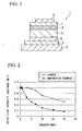
- FIG. 1 is a cross-sectional view illustrating an OLED element according to an embodiment of the invention.
- An OLED element 1 according to the embodiment has a structure in which an anode 3 formed of an ITO thin film, a hole transport layer 4, an emitting layer 5, an electron transport layer 6 made of an inorganic material such as ZnS, an electron injection layer 7, and a cathode 8 formed of a metal thin film are sequentially deposited on a substrate 2 made of a transparent material such as glass.
- an inorganic material particularly, a semiconductor material such as ZnS is used in the electron transport layer 6, which has the function of transporting electrons.
- a response time of the OLED element depends on the period of time during which electrons are injected into the cathode and recombined. The time during which the electrons move inside the electron transport layer occupies most of this period of time, and this time is evaluated based on the electron mobility of a material used in the electron transport layer and the film thickness of the electron transport layer. In this case, the film thickness of the electron transport layer may be several 10 nm in order to optimize the balance between holes and electrons in the emitting layer.
- the electron mobility of the electron transport layer may be improved. Since an inorganic material has higher electron mobility than an organic material, the response time of an OLED element using an inorganic material in the electron transport layer is faster than that of an OLED element using an organic material in the electron transport layer.
- the OLED element may be manufactured by a vapor deposition method. Forming only the electron transport layer by another manufacturing method may increase costs. Examples of the vapor deposition method include deposition of heating a resistant wire and electron beam deposition. Examples of the inorganic material which can be used to form a film by these vapor deposition methods include semiconductor materials of periodic table Groups II-VI. In particular, a compound of zinc (Zn) and sulfur (S) enhances reproducibility of the film thickness. The use of the inorganic material on the electron transport layer prevents the OLED element from deteriorating due to oxygen or moisture, thereby using the OLED element for a long time.
- a glass substrate which has dimensions of 32 mm x 25mm x 1 mm, provided with transparent electrodes made of indium tin oxide (ITO) was cleaned in isopropyl alcohol for 5 minutes by ultrasonic cleaning, and then cleaned for 5 minutes by UV ozone cleaning. After the cleaning, the glass substrate was fixed to a substrate holder, and an organic layer and a cathode are formed with a deposition apparatus for heating a resistant wire.
- ITO indium tin oxide
- the organic layer and the cathode include a hole transport layer formed of 4-4'bis[ N -(1-naphthyl)- N -phenyl-amino]biphenyl ( ⁇ -NPD) and having a thickness of 50 nm, an emitting layer formed of 0.5 mass% 5,6,11,12-tetraphenyltetracen (rubrene) doped tris(8-hydroxyquinoline)aluminum (Alq 3 ) and having a thickness of20nm, an electron transport layer formed of ZnS and having a thickness of 50 nm, an electron injection layer formed of LiF and having a thickness of 0.4 nm, and a cathode formed of Al and having a thickness of 150 nm.
- a hole transport layer formed of 4-4'bis[ N -(1-naphthyl)- N -phenyl-amino]biphenyl ( ⁇ -NPD) and having a thickness of 50 n
- a response time of the manufactured OLED element was evaluated.
- the frequency (cutoff frequency) at which the output light intensity upon applying a sinusoidal voltage of a 5 V amplitude and a 5 V bias voltage for varying a frequency is halved was measured.
- the measurement result is shown in FIG. 2 .
- a cutoff frequency of the OLED element in Example 1 was 20 MHz.
- Comparative Example 1 the OLED element, which was manufactured in the same manner as that in Example 1 except that an Alq 3 layer (thickness of 50 nm) was used instead of ZnS in the electron transport layer, was used to evaluate a response time of the OLED element.
- the cutoff frequency of the OLED element upon applying a sinusoidal voltage of a 5 V amplitude and a 5 V bias voltage was 5 MHz.
- FIG. 2 is a graph showing frequency dependency of the output light intensity of the respective OLED elements in Example 1 and Comparative Example 1. As shown in FIG. 2 , it was proven that the OLED element in Example 1 could obtain the output light intensity to some extent even though its frequency is high, compared with the OLED element in Comparative Example 1.
- emission could not be observed in the OLED element (Comparative Example 3) in which the film thickness of ZnS was more than 300 nm. The reason is thought to be that electron movement from the cathode to the emitting layer is difficult since the film thickness of ZnS is thick. In addition, emission could not be observed in the OLED element (Comparative Example 2) in which the film thickness of ZnS was 5 nm since the OLED element was broken upon applying the voltage. It is thought that the OLED element is broken since a large amount of carrier (hole or electron) flows and the electron transport layer is thin.
- the response characteristic or luminous efficiency can be further improved by adding a reducing dopant to the electron transport layer.
- a reducing dopant denotes a substance which can reduce an electron transport material (electron transporting compound). Accordingly, a substance which has a certain reducing property can be used.
- At least one substance selected from a group consisting of alkali metals, alkaline earth metals, rare earth metals, alkali metal oxides, alkali metal halides, alkaline earth metal oxides, alkaline earth metal halides, rare earth metal oxides, and rare earth metal halides can be appropriately used.
- at least one alkali metal selected form the group consisting of Na (work function: 2.4 eV), K (work function: 2.3 eV), Rb (work function: 2.2 eV), and Cs (work function: 2.0 eV) can be used.
- At least one alkali earth metal selected from the group consisting of Ca (work function: 2.9 eV), Sr (work function: 2.5 eV), and Ba (work function: 2.5 eV) can also be used.
- the luminous efficiency or the response time is improved by using a material of which the work function is 2.9 eV or less as the dopant of the electron transport layer.
- a reducing dopant may be at least one alkali metal selected from the group consisting of K, Rb, and Cs.
- Such alkali metals particularly have a high reducing capability and improvement in emission brightness or long lifetime of the OLED element can be realized just by adding a relatively small quantity to the electron injection layer.
- a combination of two or more kinds of alkali metals for example, a combination containing Cs; a combination of Cs and Na; Cs and K; Cs and Rb; or a combination of Cs, Na, and K may be used.
- the reducing capability can be efficiently improved by combining Cs and the response characteristic and luminous efficiency of the OLED element can be improved by doping to the electron transport layer.
- a glass substrate which has dimensions of 32 mm x 25mm x 1 mm, provided with transparent electrodes made of indium tin oxide (ITO) was cleaned in isopropyl alcohol for 5 minutes by ultrasonic cleaning, and then cleaned for 5 minutes by UV ozone cleaning. After the cleaning, the glass substrate was fixed to a substrate holder and an organic layer and a cathode are formed with a deposition apparatus for heating a resistant wire.
- ITO indium tin oxide
- the organic layer and the cathode include a hole transport layer formed of ⁇ -NPD and having a thickness of 50 nm, an emitting layer formed of 0.5 mass% rubrence-doped Alq 3 having a thickness of 20 nm, an electron transport layer formed of ZnS doped with alkali metals of 10 mass% and having a thickness of 50 nm, an electron injection layer formed of LiF and having a thickness of 0.4 nm, and a cathode formed of Al and having a thickness of 150 nm.
- alkali metals LiF (Example 9) and CsF (Example 10) were used as alkali metals.
- a response time of the manufactured OLED element was evaluated.
- a frequency (cutoff frequency) at which an output light intensity at a time of applying a sinusoidal voltage of a 5 V amplitude and a 5 V bias voltage for varying a frequency is halved was measured.
- the cutoff frequency of both the OLED elements was 25 MHz. Consequently, an improvement in the response time could be realized by using ZnS doping the alkali metal to the electron transport layer.
- OLED elements of examples 11 through 16 were manufactured similar to the OLED elements of examples 9 and 10 except for a doped alkali metal in the electron transport layer.
- Na, K, Nb, Cs, Sr and Ba were respectively used as the doped alkali metal.
- Na was used as the alkali metal.
- K was used.
- Nb was used.
- Cs was used.
- Sr was used.
- Ba was used.
- the cutoff frequencies of the OLED elements of the embodiments 11 through 16 were in the range of 22 MHz to 28 MHz, which is greater than the cutoff frequency of the OLED element of the embodiment 1. Therefore, the response time of the OLED element can be improved by using ZnS doping an alkali metal such as Na, K, Nb, Cs, Sr, and Ba to the electron transport layer.
- an alkali metal such as Na, K, Nb, Cs, Sr, and Ba
Landscapes
- Physics & Mathematics (AREA)
- Optics & Photonics (AREA)
- General Physics & Mathematics (AREA)
- Electroluminescent Light Sources (AREA)
Applications Claiming Priority (2)
| Application Number | Priority Date | Filing Date | Title |
|---|---|---|---|
| JP2007097300 | 2007-04-03 | ||
| JP2008095314A JP2008277799A (ja) | 2007-04-03 | 2008-04-01 | 有機エレクトロルミネッセンス素子及び光通信用モジュール |
Publications (2)
| Publication Number | Publication Date |
|---|---|
| EP1978576A2 true EP1978576A2 (de) | 2008-10-08 |
| EP1978576A3 EP1978576A3 (de) | 2012-10-17 |
Family
ID=39531300
Family Applications (1)
| Application Number | Title | Priority Date | Filing Date |
|---|---|---|---|
| EP08251286A Withdrawn EP1978576A3 (de) | 2007-04-03 | 2008-04-02 | Organisches lichtemittierendes Diodenelement und optische Verbindungsmodule |
Country Status (2)
| Country | Link |
|---|---|
| US (1) | US20080246394A1 (de) |
| EP (1) | EP1978576A3 (de) |
Cited By (2)
| Publication number | Priority date | Publication date | Assignee | Title |
|---|---|---|---|---|
| WO2011032624A1 (de) * | 2009-09-16 | 2011-03-24 | Merck Patent Gmbh | Organische elektrolumineszenzvorrichtung |
| US11476539B1 (en) | 2012-06-24 | 2022-10-18 | SeeScan, Inc. | Modular battery pack apparatus, systems, and methods including viral data and/or code transfer |
Families Citing this family (3)
| Publication number | Priority date | Publication date | Assignee | Title |
|---|---|---|---|---|
| JP5722220B2 (ja) * | 2009-08-18 | 2015-05-20 | 大電株式会社 | 有機電界発光素子 |
| CN102592543A (zh) * | 2012-03-09 | 2012-07-18 | 郭丰亮 | 基于oled可见光通信的显示器 |
| CN106549113B (zh) * | 2017-01-16 | 2019-10-01 | 上海天马有机发光显示技术有限公司 | 一种有机发光显示面板及装置 |
Citations (9)
| Publication number | Priority date | Publication date | Assignee | Title |
|---|---|---|---|---|
| JPH0529080A (ja) | 1990-11-28 | 1993-02-05 | Idemitsu Kosan Co Ltd | 有機エレクトロルミネツセンス素子および該素子を用いた発光装置 |
| JPH11354283A (ja) | 1998-04-08 | 1999-12-24 | Idemitsu Kosan Co Ltd | 有機エレクトロルミネッセンス素子 |
| JP2000164363A (ja) | 1998-11-25 | 2000-06-16 | Idemitsu Kosan Co Ltd | 有機エレクトロルミネッセンス素子 |
| JP2002164178A (ja) | 2000-11-27 | 2002-06-07 | Idemitsu Kosan Co Ltd | 有機エレクトロルミネッセンス素子 |
| JP2002313553A (ja) | 2001-04-06 | 2002-10-25 | Kansai Tlo Kk | 高速動作有機el素子 |
| JP2003014995A (ja) | 2001-07-04 | 2003-01-15 | Fuji Photo Film Co Ltd | 光伝送モジュール、及び光トランシーバ |
| JP2003149541A (ja) | 2001-11-09 | 2003-05-21 | Fuji Photo Optical Co Ltd | 被写体距離表示装置 |
| JP2003238534A (ja) | 2002-02-22 | 2003-08-27 | Idemitsu Kosan Co Ltd | 新規アントラセン化合物およびそれを用いた有機エレクトロルミネッセンス素子 |
| JP2003243157A (ja) | 2002-02-20 | 2003-08-29 | Osaka Industrial Promotion Organization | 有機el素子の駆動方法および有機el素子を含む発光装置 |
Family Cites Families (8)
| Publication number | Priority date | Publication date | Assignee | Title |
|---|---|---|---|---|
| GB9907120D0 (en) * | 1998-12-16 | 1999-05-19 | Cambridge Display Tech Ltd | Organic light-emissive devices |
| EP1347031A4 (de) * | 2000-09-07 | 2007-07-04 | Idemitsu Kosan Co | Organisches elektrolumineszierendes element |
| US20030007736A1 (en) * | 2001-07-04 | 2003-01-09 | Fuji Photo Film Co., Ltd. | Optical transmission module and optical transceiver |
| US20040069202A1 (en) * | 2002-06-04 | 2004-04-15 | Courtheyn Steven Michael | Grab all gripping anchor |
| JP4689176B2 (ja) * | 2004-02-26 | 2011-05-25 | 大日本印刷株式会社 | 有機エレクトロルミネッセンス素子 |
| GB0422913D0 (en) * | 2004-10-15 | 2004-11-17 | Elam T Ltd | Electroluminescent devices |
| DE102005032593B4 (de) * | 2005-07-11 | 2007-07-26 | Technische Universität Berlin | Optisches Modul mit einer Leichtleitfaser und einem lichtemittierenden/lichtempfangenden Bauteil und Verfahren zum Herstellen |
| KR20070035341A (ko) * | 2005-09-27 | 2007-03-30 | 삼성전자주식회사 | 간극을 채운 반도체 나노결정층을 함유하는 발광소자 및 그제조방법 |
-
2008
- 2008-04-02 US US12/061,537 patent/US20080246394A1/en not_active Abandoned
- 2008-04-02 EP EP08251286A patent/EP1978576A3/de not_active Withdrawn
Patent Citations (9)
| Publication number | Priority date | Publication date | Assignee | Title |
|---|---|---|---|---|
| JPH0529080A (ja) | 1990-11-28 | 1993-02-05 | Idemitsu Kosan Co Ltd | 有機エレクトロルミネツセンス素子および該素子を用いた発光装置 |
| JPH11354283A (ja) | 1998-04-08 | 1999-12-24 | Idemitsu Kosan Co Ltd | 有機エレクトロルミネッセンス素子 |
| JP2000164363A (ja) | 1998-11-25 | 2000-06-16 | Idemitsu Kosan Co Ltd | 有機エレクトロルミネッセンス素子 |
| JP2002164178A (ja) | 2000-11-27 | 2002-06-07 | Idemitsu Kosan Co Ltd | 有機エレクトロルミネッセンス素子 |
| JP2002313553A (ja) | 2001-04-06 | 2002-10-25 | Kansai Tlo Kk | 高速動作有機el素子 |
| JP2003014995A (ja) | 2001-07-04 | 2003-01-15 | Fuji Photo Film Co Ltd | 光伝送モジュール、及び光トランシーバ |
| JP2003149541A (ja) | 2001-11-09 | 2003-05-21 | Fuji Photo Optical Co Ltd | 被写体距離表示装置 |
| JP2003243157A (ja) | 2002-02-20 | 2003-08-29 | Osaka Industrial Promotion Organization | 有機el素子の駆動方法および有機el素子を含む発光装置 |
| JP2003238534A (ja) | 2002-02-22 | 2003-08-27 | Idemitsu Kosan Co Ltd | 新規アントラセン化合物およびそれを用いた有機エレクトロルミネッセンス素子 |
Cited By (3)
| Publication number | Priority date | Publication date | Assignee | Title |
|---|---|---|---|---|
| WO2011032624A1 (de) * | 2009-09-16 | 2011-03-24 | Merck Patent Gmbh | Organische elektrolumineszenzvorrichtung |
| CN102498587A (zh) * | 2009-09-16 | 2012-06-13 | 默克专利有限公司 | 有机电致发光器件 |
| US11476539B1 (en) | 2012-06-24 | 2022-10-18 | SeeScan, Inc. | Modular battery pack apparatus, systems, and methods including viral data and/or code transfer |
Also Published As
| Publication number | Publication date |
|---|---|
| US20080246394A1 (en) | 2008-10-09 |
| EP1978576A3 (de) | 2012-10-17 |
Similar Documents
| Publication | Publication Date | Title |
|---|---|---|
| JP4898560B2 (ja) | 有機発光装置 | |
| US6111274A (en) | Inorganic light emitting diode | |
| US6379824B1 (en) | Organic electroluminescence device | |
| KR20020086281A (ko) | 고 콘트라스트 발광 다이오드 장치 | |
| US20060152150A1 (en) | Electroluminescent display with improved light outcoupling | |
| KR100621442B1 (ko) | 유기 전계발광 소자, 이 유기 전계발광 소자의 제조 방법,및 유기 전계발광 표시 장치 | |
| US6180963B1 (en) | Light emitting diode | |
| EP1978576A2 (de) | Organisches lichtemittierendes Diodenelement und optische Verbindungsmodule | |
| KR100610179B1 (ko) | 일렉트로루미네선스 소자 및 그 제조 방법 | |
| KR20080090349A (ko) | 유기발광 다이오드 소자 및 광통신용 모듈 | |
| KR100790672B1 (ko) | 유기 일렉트로루미네센스 소자 및 유기 일렉트로루미네센스디스플레이 | |
| EP1944349A1 (de) | Organisches Elektrolumineszenz- und optisches Verbindungsmodul | |
| KR100699966B1 (ko) | 유기 일렉트로루미네선스 소자 및 유기 일렉트로루미네선스디스플레이 | |
| EP1009045A2 (de) | Organische elektrolumineszente Vorrichtung | |
| US20090243471A1 (en) | Organic electroluminescent device | |
| KR100820106B1 (ko) | 유기전기발광소자의 제조방법 | |
| US20250143072A1 (en) | Amorphous metal based top emission organic light emitting diodes | |
| JP2025117840A (ja) | 有機el素子 | |
| KR19990026907A (ko) | 유기전계발광소자 및 그 제조방법 | |
| EP0967668A2 (de) | Organische elektrolumineszente Vorrichtung | |
| JP2009110770A (ja) | 有機エレクトロルミネッセンス素子及び光インターコネクション | |
| KR100683694B1 (ko) | 유기전계 발광표시장치 | |
| JP2007242829A (ja) | 有機el素子およびその製造方法 | |
| JP2009176762A (ja) | 有機エレクトロルミネッセンス素子及び光配線モジュール | |
| KR20150066037A (ko) | 산화아연계 스퍼터링 타겟, 이를 통해 증착된 투명전극을 갖는 유기발광소자 및 그 제조방법 |
Legal Events
| Date | Code | Title | Description |
|---|---|---|---|
| PUAI | Public reference made under article 153(3) epc to a published international application that has entered the european phase |
Free format text: ORIGINAL CODE: 0009012 |
|
| 17P | Request for examination filed |
Effective date: 20080418 |
|
| AK | Designated contracting states |
Kind code of ref document: A2 Designated state(s): AT BE BG CH CY CZ DE DK EE ES FI FR GB GR HR HU IE IS IT LI LT LU LV MC MT NL NO PL PT RO SE SI SK TR |
|
| AX | Request for extension of the european patent |
Extension state: AL BA MK RS |
|
| PUAL | Search report despatched |
Free format text: ORIGINAL CODE: 0009013 |
|
| AK | Designated contracting states |
Kind code of ref document: A3 Designated state(s): AT BE BG CH CY CZ DE DK EE ES FI FR GB GR HR HU IE IS IT LI LT LU LV MC MT NL NO PL PT RO SE SI SK TR |
|
| AX | Request for extension of the european patent |
Extension state: AL BA MK RS |
|
| RIC1 | Information provided on ipc code assigned before grant |
Ipc: H01L 51/54 20060101AFI20120912BHEP Ipc: H01L 51/52 20060101ALI20120912BHEP Ipc: G02B 6/42 20060101ALI20120912BHEP |
|
| AKX | Designation fees paid |
Designated state(s): DE FI FR GB |
|
| STAA | Information on the status of an ep patent application or granted ep patent |
Free format text: STATUS: THE APPLICATION IS DEEMED TO BE WITHDRAWN |
|
| 18D | Application deemed to be withdrawn |
Effective date: 20130418 |