EP0454440B1 - Verfahren zur Einkapselung einer Halbleitervorrichtung - Google Patents
Verfahren zur Einkapselung einer Halbleitervorrichtung Download PDFInfo
- Publication number
- EP0454440B1 EP0454440B1 EP91303688A EP91303688A EP0454440B1 EP 0454440 B1 EP0454440 B1 EP 0454440B1 EP 91303688 A EP91303688 A EP 91303688A EP 91303688 A EP91303688 A EP 91303688A EP 0454440 B1 EP0454440 B1 EP 0454440B1
- Authority
- EP
- European Patent Office
- Prior art keywords
- chip
- lead
- finger portions
- resin
- peripheral portion
- Prior art date
- Legal status (The legal status is an assumption and is not a legal conclusion. Google has not performed a legal analysis and makes no representation as to the accuracy of the status listed.)
- Expired - Lifetime
Links
Images


Classifications
-
- B—PERFORMING OPERATIONS; TRANSPORTING
- B29—WORKING OF PLASTICS; WORKING OF SUBSTANCES IN A PLASTIC STATE IN GENERAL
- B29C—SHAPING OR JOINING OF PLASTICS; SHAPING OF MATERIAL IN A PLASTIC STATE, NOT OTHERWISE PROVIDED FOR; AFTER-TREATMENT OF THE SHAPED PRODUCTS, e.g. REPAIRING
- B29C45/00—Injection moulding, i.e. forcing the required volume of moulding material through a nozzle into a closed mould; Apparatus therefor
- B29C45/14—Injection moulding, i.e. forcing the required volume of moulding material through a nozzle into a closed mould; Apparatus therefor incorporating preformed parts or layers, e.g. injection moulding around inserts or for coating articles
- B29C45/14639—Injection moulding, i.e. forcing the required volume of moulding material through a nozzle into a closed mould; Apparatus therefor incorporating preformed parts or layers, e.g. injection moulding around inserts or for coating articles for obtaining an insulating effect, e.g. for electrical components
- B29C45/14655—Injection moulding, i.e. forcing the required volume of moulding material through a nozzle into a closed mould; Apparatus therefor incorporating preformed parts or layers, e.g. injection moulding around inserts or for coating articles for obtaining an insulating effect, e.g. for electrical components connected to or mounted on a carrier, e.g. lead frame
-
- H10W76/12—
-
- H10W70/411—
-
- H10W72/0198—
-
- H10W74/016—
-
- H10W74/111—
-
- H10W74/00—
-
- H10W74/10—
-
- H10W90/756—
Definitions
- This invention relates to a method of manufacturing a semiconductor device.
- FIG. 4 of the accompanying drawings shows a known "die pad" construction in which a chip c is bonded to a die-pad a by a bonding material d , such as a silver paste or a gold-silicon eutectic alloy.
- the die-pad a is connected to a peripheral portion of a lead frame by connecting fingers a ′.
- a plurality of lead fingers b project from the peripheral portion of the lead frame, and each lead finger b is connected to a respective electrode of the chip c by a respective bonding wire e .
- the chip c , die-pad a , bonding wires e and inner ends of the fingers a ′, b are then placed in a moulding die and sealed in a resin package.
- FIG. 5 Another known "chip-on-lead" type of construction is shown in Figure 5.
- an insulator f such as a polyimide sheet, is placed on the inner ends of lead fingers b , a semiconductor chip c is placed on the insulator f and the electrodes of the semiconductor chip c are connected to respective inner ends of the lead fingers b by respective bonding wires e . Again, the assembly is then sealed in a resin package.
- FIG. 6 A further known "lead-on-chip" type of construction is shown in Figure 6.
- a surface of a semiconductor chip c excluding the electrodes thereon, is covered with an insulator f , lead fingers b are placed on the insulator f , and the lead fingers b are connected to respective electrodes by respective bonding wires e .
- the assembly is then sealed in a resin package.
- Figure 7 shows a known "directly connected" form of construction, in which electrode pads g of a semiconductor chip c project upwardly from the upper surface of the chip c , and the inner ends of lead fingers b are directly connected to the electrode pads g . The assembly is then sealed in a resin package.
- the height of the semiconductor device is as small as possible.
- the thickness of the die pad a and bonding material d add to the height of the package.
- the thickness of the insulators f and the lead fingers b add to the height of the package.
- the thickness of the lead fingers b and the height of the electrode pads g add to the overall height of the semiconductor package.
- the die pad construction suffers from the problem that thermal stress is induced in the device due to differences in the coefficients of thermal expansion of the die pad a , the semiconductor chip c and the resin of the package, which can cause a breakdown in bonding between the chip c and the die pad a , between the die pad a and the resin package, or between the chip c and the resin package.
- the problems with which the present invention are concerned are: to enable a semiconductor device to be produced which has a decreased height; to alleviate thermal stresses in the semiconductor package; and/or to enable the semiconductor device to be produced reliably, such that there is a small risk of the bonding wires being broken or short circuited while the resin package is being formed around the assembly of the chip, bonding wires and lead fingers.
- Patent Abstracts of Japan abstract of Patent Application JP-A-60-037754 and Patent Application EP-A-0 366 386 each show a chip package with no die pad, and with bonding wires extending between the lead fingers and electrode pads, but do not address the problem of the bonding wires being broken or short-circuited while the plastics package is being formed.
- Patent Abstracts of Japan abstract of Patent Application JP-A-01-262115 shows a lead on chip construction and a mould which has sliding pins which engage the leads on top of the chip and the underside of the chip during plastics injection to hold the chip.
- a method of manufacturing a semiconductor device comprising the steps of: providing a semiconductor chip, the semiconductor chip having an upper surface and a lower surface and having a plurality of electrodes formed on said upper surface; providing a lead frame having no die pad, the lead frame comprising a peripheral portion surrounding a region for receiving the chip and a plurality of lead finger portions and movement restricting finger portions projecting from the peripheral portion towards said region and terminating outside said region; placing the chip in said region such that said lead finger portions and said movement restricting finger portions do not contact said chip; connecting each of the electrodes to a respective one of the lead finger portions with a respective bonding wire; providing a mould having a mould cavity and at least one projection projecting into said cavity; placing said chip in said mould cavity such that said projection projects towards but does not contact said upper or lower surfaces of said chip; injecting resin into said mould cavity, thereby sealing the chip and bonding wires in a resin package such that the lead finger portions project out of the package and such that the resin package directly contacts
- a lead frame 1 for manufacturing a plurality of semiconductor devices has apertures 2 for receiving semiconductor chips 7 in a longitudinal arrangement at regular intervals.
- the apertures 2 are provided instead of the die pads in the known die pad form of construction.
- Each aperture 2 is of a size such that the respective chip 7 could be passed through the aperture.
- the lead frame 1 has peripheral frame members 5 surrounding each aperture 2, tie bars 4 connecting portions of the lead frame for each chip, lead fingers 3 projecting towards each aperture 2 and horizontal movement restricting fingers 6 projecting inwardly from the side portions of the frame members 5 towards the apertures 2.
- Each semiconductor chip 7 is placed in the respective aperture 2.
- the size of the aperture 2 (defined by inner ends of the lead fingers 3 and movement restricting fingers 6) is such that the lead fingers 3 and the movement restricting fingers 6 do not contact the chip 7.
- Each chip 7 has a plurality of electrodes 9, and each electrode is connected to the inner end of a respective one of the lead fingers 3 by a respective bonding wire 8. Thus, each semiconductor chip 7 is connected to the lead frame 1 solely by the bonding wires 8.
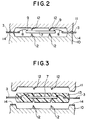
- the lead frame 1, with the chips 7 connected thereto, is placed in a moulding die, as shown in Figure 2.
- the moulding die comprises a lower die part 10 and a complementary upper die part 11, and the lead fingers and movement restricting fingers pass through channels 14 between the die parts 10,11.
- Both die parts 10,11 are provided with vertical movement restricting pins 12, which project towards the chip 7, but which are slightly separated from the upper and lower surfaces of the chip 7.
- resin is injected into the mould cavity of the moulding die to seal the semiconductor chip, the bonding wires 8, and the inner ends of the lead fingers 3 within a resin package 13 as shown in Figure 3.
- the resin has a sufficiently low viscosity in the initial stage of injection of resin into the mould cavity, the resin tends to urge the chip 7 vertically either towards the lower die part 10 or the upper die part 11, due to slight differences in resistance against the flow of the resin between the upper and lower surfaces of the semiconductor chip 7.
- vertical movement of the chip 7 is restricted by the vertical movement restricting projections 12, so that the chip 7 cannot significantly move towards the lower die part 10 or upper die part 11.
- the resin becomes distributed uniformly within the mould cavity, and the resin tends to fill the gaps between the tips of the vertical movement restricting projections 12 and the upper and lower surfaces of the chip 7.
- the chip 7 tends to return to its original position within the moulding die, and therefore partial exposure of the chip 7 at the locations of the movement restricting projections 12 is unlikely to occur.
- the viscosity of the resin being injected may also tend to urge the chip sideways in the mould cavity.
- sideways movement of the chip is restricted not only by the bonding wires 8, but also by the horizontal movement restricting fingers 6. Even if the tip of one or more of the horizontal movement restricting fingers 6 possibly remains in contact with a side surface of the chip 7 after the resin has hardened, no problem arises because the portions of the horizontal movement restricting projections which project outside the resin package 13 are subsequently cut off.
- the lower and upper die parts 10,11 are separated, and the lead frame with the packages moulded thereon are removed. Then, the horizontal movement restricting portions 6 are cut off flush with the side of each package 13, and the lead fingers 3 are severed each at a location spaced from the resin package so as to form individual connecting leads for the chips.
Landscapes
- Engineering & Computer Science (AREA)
- Manufacturing & Machinery (AREA)
- Mechanical Engineering (AREA)
- Encapsulation Of And Coatings For Semiconductor Or Solid State Devices (AREA)
- Structures Or Materials For Encapsulating Or Coating Semiconductor Devices Or Solid State Devices (AREA)
- Lead Frames For Integrated Circuits (AREA)
Claims (3)
- Verfahren zur Herstellung einer Halbleitereinrichtung, das folgende Schritte aufweist:
Bereitstellen eines Halbleiterchips (7), wobei der Halbleiterchip eine obere Oberfläche und eine untere Oberfläche hat und eine Vielzahl von Elektroden (9), die auf der oberen Oberfläche gebildet sind;
Bereitstellen eines Systemträgers (1), der keinen Kontaktfleck hat, wobei der Systemträger einen peripheren Bereich (5) aufweist, der einen Bereich zur Aufnahme des Chips und einer Vielzahl von Leiterbahnfingerbereichen (3) und Bewegungsbeschränkungsfingerbereichen (6) umgibt, die sich vom peripheren Bereich in Richtung auf diesen Bereich erstrecken und an der Außenseite dieses Bereichs enden;
Anordnen des Chips in diesem Bereich so, daß die Leiterbahnfingerbereiche (3) und die Bewegungsbeschränkungsfingerbereiche (6) nicht den Chip (7) berühren;
Kontaktieren jeder der Elektroden mit einem entsprechenden der Leiterbahnfingerbereiche mit einem entsprechenden Bonddraht (8);
Bereitstellen einer Form (10, 11) mit einer Formmulde und zumindest einem Ansatz (12), der in die Mulde hineinragt;
Anordnen des Chips in dieser Formmulde, so daß dieser Ansatz (12) sich in Richtung auf den Chip erstreckt, jedoch nicht die obere oder untere Oberfläche des Chips berührt;
Einspritzen von Kunststoff in die Formmulde, wodurch der Chip und die Bonddrähte zu einem Kunststoffgehäuse (13) vergossen werden, so daß die Leiterbahnfingerbereiche aus dem Gehäuse herausragen und das Kunststoffgehäuse unmittelbar sowohl die obere Oberfläche als auch die untere Oberfläche des Chips berührt, und
Abtrennen eines jeden der Leiterbahnfingerbereiche vom peripheren Bereich des Rahmens. - Verfahren nach Anspruch 1, wobei unmittelbar vor dem Einspritzungsschritt der Chip mechanisch mit dem peripheren Bereich lediglich durch die Bonddrähte und die Leiterbahnfingerbereiche kontaktiert wird.
- Verfahren nach Anspruch 1 oder 2, wobei die Form eine Vielzahl von Ansätzen (12) aufweist, die sich in Richtung auf den Chip erstrecken, jedoch nicht die obere und untere Oberfläche des Chips berühren, wenn der Chip in der Formmulde angeordnet wird.
Applications Claiming Priority (2)
| Application Number | Priority Date | Filing Date | Title |
|---|---|---|---|
| JP109934/90 | 1990-04-25 | ||
| JP2109934A JP2890662B2 (ja) | 1990-04-25 | 1990-04-25 | 樹脂封止型半導体装置の製造方法とそれに用いるリードフレーム |
Publications (2)
| Publication Number | Publication Date |
|---|---|
| EP0454440A1 EP0454440A1 (de) | 1991-10-30 |
| EP0454440B1 true EP0454440B1 (de) | 1995-09-06 |
Family
ID=14522816
Family Applications (1)
| Application Number | Title | Priority Date | Filing Date |
|---|---|---|---|
| EP91303688A Expired - Lifetime EP0454440B1 (de) | 1990-04-25 | 1991-04-24 | Verfahren zur Einkapselung einer Halbleitervorrichtung |
Country Status (5)
| Country | Link |
|---|---|
| US (1) | US5289033A (de) |
| EP (1) | EP0454440B1 (de) |
| JP (1) | JP2890662B2 (de) |
| KR (1) | KR100222349B1 (de) |
| DE (1) | DE69112693T2 (de) |
Cited By (1)
| Publication number | Priority date | Publication date | Assignee | Title |
|---|---|---|---|---|
| DE10227936C1 (de) * | 2002-06-21 | 2003-05-15 | Heraeus Gmbh W C | Verfahren zur Herstellung von Systemträgern aus metallischem Trägerband sowie Metallstreifen mit Trägerbereich für elektrische Bauelemente |
Families Citing this family (17)
| Publication number | Priority date | Publication date | Assignee | Title |
|---|---|---|---|---|
| US4956423A (en) * | 1985-10-29 | 1990-09-11 | Occidental Chemical Corporation | Hot-melt adhesives |
| FI90850C (fi) * | 1992-05-29 | 1994-04-11 | Idesco Oy | Menetelmä muovista ruiskuvalettavan kuljetus- tai säilytysrakenteen varustamiseksi etäluettavalla saattomuistilla ja etäluettavalla saattomuistilla varustettu muovista ruiskuvalettu kuljetus- tai säilytysrakenne |
| DE4231705C2 (de) * | 1992-09-22 | 1998-04-30 | Siemens Ag | Halbleitervorrichtung mit einem Systemträger und einem damit verbundenen Halbleiterchip sowie Verfahren zu deren Herstellung |
| JPH07273669A (ja) * | 1992-12-21 | 1995-10-20 | Sony Corp | エラー訂正方法 |
| US5474958A (en) * | 1993-05-04 | 1995-12-12 | Motorola, Inc. | Method for making semiconductor device having no die supporting surface |
| US6148673A (en) * | 1994-10-07 | 2000-11-21 | Motorola, Inc. | Differential pressure sensor and method thereof |
| US5660461A (en) * | 1994-12-08 | 1997-08-26 | Quantum Devices, Inc. | Arrays of optoelectronic devices and method of making same |
| JP3290869B2 (ja) * | 1995-11-16 | 2002-06-10 | 株式会社東芝 | 半導体装置 |
| JPH1117557A (ja) * | 1997-05-01 | 1999-01-22 | Mitsubishi Electric Corp | 誤り訂正方法及び誤り訂正装置 |
| JPH11274196A (ja) * | 1998-03-26 | 1999-10-08 | Seiko Epson Corp | 半導体装置の製造方法およびモールドシステム並びに半導体装置 |
| DE10243515A1 (de) * | 2002-09-19 | 2004-04-01 | Robert Bosch Gmbh | Sensor |
| DE10247610A1 (de) * | 2002-10-11 | 2004-04-29 | Micronas Gmbh | Elektronisches Bauelement mit einem Systemträger |
| US20040113240A1 (en) | 2002-10-11 | 2004-06-17 | Wolfgang Hauser | An electronic component with a leadframe |
| US8080444B2 (en) * | 2010-01-14 | 2011-12-20 | Freescale Semiconductor, Inc. | Method for forming a packaged semiconductor device having a ground plane |
| JP6104545B2 (ja) * | 2012-09-19 | 2017-03-29 | シャープ株式会社 | 半導体装置の製造方法、および成形部材 |
| JP2019121722A (ja) * | 2018-01-10 | 2019-07-22 | 株式会社ディスコ | パッケージ基板の製造方法 |
| US12142549B2 (en) * | 2018-07-03 | 2024-11-12 | Texas Instruments Incorporated | Wafer stencil for controlling die attach material thickness on die |
Family Cites Families (19)
| Publication number | Priority date | Publication date | Assignee | Title |
|---|---|---|---|---|
| US3802069A (en) * | 1972-05-04 | 1974-04-09 | Gte Sylvania Inc | Fabricating packages for use in integrated circuits |
| US4012766A (en) * | 1973-08-28 | 1977-03-15 | Western Digital Corporation | Semiconductor package and method of manufacture thereof |
| US4069924A (en) * | 1976-11-18 | 1978-01-24 | Western Electric Co., Inc. | Methods and apparatus for positioning an article laterally on a support |
| US4255851A (en) * | 1978-12-06 | 1981-03-17 | Western Electric Company, Inc. | Method and apparatus for indelibly marking articles during a manufacturing process |
| US4330790A (en) * | 1980-03-24 | 1982-05-18 | National Semiconductor Corporation | Tape operated semiconductor device packaging |
| US4331740A (en) * | 1980-04-14 | 1982-05-25 | National Semiconductor Corporation | Gang bonding interconnect tape process and structure for semiconductor device automatic assembly |
| JPS6037754A (ja) * | 1983-08-10 | 1985-02-27 | Seiko Epson Corp | フラツトパツケ−ジ |
| US4812421A (en) * | 1987-10-26 | 1989-03-14 | Motorola, Inc. | Tab-type semiconductor process |
| GB2178894B (en) * | 1985-08-06 | 1988-07-27 | Gen Electric Co Plc | Preparation of fragile devices |
| US4756080A (en) * | 1986-01-27 | 1988-07-12 | American Microsystems, Inc. | Metal foil semiconductor interconnection method |
| JPS6331149A (ja) * | 1986-07-25 | 1988-02-09 | Fujitsu Ltd | 半導体装置 |
| US4884124A (en) * | 1986-08-19 | 1989-11-28 | Mitsubishi Denki Kabushiki Kaisha | Resin-encapsulated semiconductor device |
| US4855807A (en) * | 1986-12-26 | 1989-08-08 | Kabushiki Kaisha Toshiba | Semiconductor device |
| US4806409A (en) * | 1987-05-20 | 1989-02-21 | Olin Corporation | Process for providing an improved electroplated tape automated bonding tape and the product produced thereby |
| JPH01262115A (ja) * | 1988-04-14 | 1989-10-19 | Seiko Epson Corp | Ic封止用射出成形金型 |
| US4994895A (en) * | 1988-07-11 | 1991-02-19 | Fujitsu Limited | Hybrid integrated circuit package structure |
| US5018003A (en) * | 1988-10-20 | 1991-05-21 | Mitsubishi Denki Kabushiki Kaisha | Lead frame and semiconductor device |
| US4924291A (en) * | 1988-10-24 | 1990-05-08 | Motorola Inc. | Flagless semiconductor package |
| JPH02134852A (ja) * | 1988-11-15 | 1990-05-23 | Nec Corp | 樹脂封止型半導体装置 |
-
1990
- 1990-04-25 JP JP2109934A patent/JP2890662B2/ja not_active Expired - Fee Related
-
1991
- 1991-04-24 EP EP91303688A patent/EP0454440B1/de not_active Expired - Lifetime
- 1991-04-24 US US07/690,358 patent/US5289033A/en not_active Expired - Fee Related
- 1991-04-24 DE DE69112693T patent/DE69112693T2/de not_active Expired - Fee Related
- 1991-04-25 KR KR1019910006637A patent/KR100222349B1/ko not_active Expired - Fee Related
Cited By (1)
| Publication number | Priority date | Publication date | Assignee | Title |
|---|---|---|---|---|
| DE10227936C1 (de) * | 2002-06-21 | 2003-05-15 | Heraeus Gmbh W C | Verfahren zur Herstellung von Systemträgern aus metallischem Trägerband sowie Metallstreifen mit Trägerbereich für elektrische Bauelemente |
Also Published As
| Publication number | Publication date |
|---|---|
| US5289033A (en) | 1994-02-22 |
| KR910019187A (ko) | 1991-11-30 |
| JPH047848A (ja) | 1992-01-13 |
| JP2890662B2 (ja) | 1999-05-17 |
| KR100222349B1 (ko) | 1999-10-01 |
| DE69112693T2 (de) | 1996-02-01 |
| DE69112693D1 (de) | 1995-10-12 |
| EP0454440A1 (de) | 1991-10-30 |
Similar Documents
| Publication | Publication Date | Title |
|---|---|---|
| EP0454440B1 (de) | Verfahren zur Einkapselung einer Halbleitervorrichtung | |
| US5214846A (en) | Packaging of semiconductor chips | |
| US7410834B2 (en) | Method of manufacturing a semiconductor device | |
| US6707138B2 (en) | Semiconductor device including metal strap electrically coupled between semiconductor die and metal leadframe | |
| US8497158B2 (en) | Leadframe strip and mold apparatus for an electronic component and method of encapsulating an electronic component | |
| JPH06252316A (ja) | リードフレーム上へのプラスチック部材の形成方法 | |
| US20020039811A1 (en) | A method of manufacturing a semiconductor device | |
| US7301225B2 (en) | Multi-row lead frame | |
| JPH088280A (ja) | 電子部品及びその製造方法 | |
| JP3877409B2 (ja) | 半導体装置の製造方法 | |
| US6476478B1 (en) | Cavity semiconductor package with exposed leads and die pad | |
| JP3877410B2 (ja) | 半導体装置の製造方法 | |
| EP4485525A1 (de) | Qfn-verkapselte halbleiteranordnung und verfahren zu deren herstellung | |
| JP2983105B2 (ja) | 半導体装置およびその製法 | |
| KR100454774B1 (ko) | 반도체장치 | |
| JP2973901B2 (ja) | 半導体樹脂封止用金型 | |
| JPH0653264A (ja) | 半導体装置の製造方法 | |
| JPH05102217A (ja) | 半導体装置およびその製造方法並びにそれに使用される成形装置 | |
| JPH04317363A (ja) | ダイパッドレス樹脂封止型半導体装置とその製造方法 | |
| KR19990012316A (ko) | 반도체 패키지의 몰딩 금형 장치 | |
| JPH039538A (ja) | 半導体装置用樹脂封止金型 | |
| JP2000114448A (ja) | 半導体装置およびその製造方法 | |
| JPH1027870A (ja) | 半導体装置およびその製造方法 | |
| JPS6058647A (ja) | 樹脂封止体 | |
| JP2003203935A (ja) | 半導体装置の封止方法およびそれに用いる封止装置 |
Legal Events
| Date | Code | Title | Description |
|---|---|---|---|
| PUAI | Public reference made under article 153(3) epc to a published international application that has entered the european phase |
Free format text: ORIGINAL CODE: 0009012 |
|
| AK | Designated contracting states |
Kind code of ref document: A1 Designated state(s): DE FR GB |
|
| 17P | Request for examination filed |
Effective date: 19920327 |
|
| 17Q | First examination report despatched |
Effective date: 19940530 |
|
| GRAA | (expected) grant |
Free format text: ORIGINAL CODE: 0009210 |
|
| AK | Designated contracting states |
Kind code of ref document: B1 Designated state(s): DE FR GB |
|
| REF | Corresponds to: |
Ref document number: 69112693 Country of ref document: DE Date of ref document: 19951012 |
|
| ET | Fr: translation filed | ||
| PLBE | No opposition filed within time limit |
Free format text: ORIGINAL CODE: 0009261 |
|
| STAA | Information on the status of an ep patent application or granted ep patent |
Free format text: STATUS: NO OPPOSITION FILED WITHIN TIME LIMIT |
|
| 26N | No opposition filed | ||
| REG | Reference to a national code |
Ref country code: GB Ref legal event code: IF02 |
|
| PGFP | Annual fee paid to national office [announced via postgrant information from national office to epo] |
Ref country code: FR Payment date: 20030408 Year of fee payment: 13 |
|
| PGFP | Annual fee paid to national office [announced via postgrant information from national office to epo] |
Ref country code: GB Payment date: 20030423 Year of fee payment: 13 |
|
| PGFP | Annual fee paid to national office [announced via postgrant information from national office to epo] |
Ref country code: DE Payment date: 20030502 Year of fee payment: 13 |
|
| PG25 | Lapsed in a contracting state [announced via postgrant information from national office to epo] |
Ref country code: GB Free format text: LAPSE BECAUSE OF NON-PAYMENT OF DUE FEES Effective date: 20040424 |
|
| PG25 | Lapsed in a contracting state [announced via postgrant information from national office to epo] |
Ref country code: DE Free format text: LAPSE BECAUSE OF NON-PAYMENT OF DUE FEES Effective date: 20041103 |
|
| GBPC | Gb: european patent ceased through non-payment of renewal fee |
Effective date: 20040424 |
|
| PG25 | Lapsed in a contracting state [announced via postgrant information from national office to epo] |
Ref country code: FR Free format text: LAPSE BECAUSE OF NON-PAYMENT OF DUE FEES Effective date: 20041231 |
|
| REG | Reference to a national code |
Ref country code: FR Ref legal event code: ST |