EP0351868B1 - Dispositif électroluminescent à semi-conducteur composé - Google Patents
Dispositif électroluminescent à semi-conducteur composé Download PDFInfo
- Publication number
- EP0351868B1 EP0351868B1 EP89113442A EP89113442A EP0351868B1 EP 0351868 B1 EP0351868 B1 EP 0351868B1 EP 89113442 A EP89113442 A EP 89113442A EP 89113442 A EP89113442 A EP 89113442A EP 0351868 B1 EP0351868 B1 EP 0351868B1
- Authority
- EP
- European Patent Office
- Prior art keywords
- zns
- znse
- light
- substrate
- group
- Prior art date
- Legal status (The legal status is an assumption and is not a legal conclusion. Google has not performed a legal analysis and makes no representation as to the accuracy of the status listed.)
- Expired - Lifetime
Links
- 239000004065 semiconductor Substances 0.000 title claims description 63
- 150000001875 compounds Chemical class 0.000 title claims description 54
- 239000000758 substrate Substances 0.000 claims description 81
- 239000012535 impurity Substances 0.000 claims description 33
- 229910052751 metal Inorganic materials 0.000 claims description 8
- 239000002184 metal Substances 0.000 claims description 8
- 229910052740 iodine Inorganic materials 0.000 claims description 6
- 238000005401 electroluminescence Methods 0.000 claims description 2
- 239000012212 insulator Substances 0.000 claims description 2
- SBIBMFFZSBJNJF-UHFFFAOYSA-N selenium;zinc Chemical compound [Se]=[Zn] SBIBMFFZSBJNJF-UHFFFAOYSA-N 0.000 claims 22
- PFNQVRZLDWYSCW-UHFFFAOYSA-N (fluoren-9-ylideneamino) n-naphthalen-1-ylcarbamate Chemical compound C12=CC=CC=C2C2=CC=CC=C2C1=NOC(=O)NC1=CC=CC2=CC=CC=C12 PFNQVRZLDWYSCW-UHFFFAOYSA-N 0.000 description 54
- 239000005083 Zinc sulfide Substances 0.000 description 36
- 229910052984 zinc sulfide Inorganic materials 0.000 description 36
- 239000013078 crystal Substances 0.000 description 21
- 239000010931 gold Substances 0.000 description 14
- 238000000034 method Methods 0.000 description 11
- 238000001451 molecular beam epitaxy Methods 0.000 description 11
- 238000010586 diagram Methods 0.000 description 9
- NINIDFKCEFEMDL-UHFFFAOYSA-N Sulfur Chemical compound [S] NINIDFKCEFEMDL-UHFFFAOYSA-N 0.000 description 8
- 229910052782 aluminium Inorganic materials 0.000 description 8
- 229910052717 sulfur Inorganic materials 0.000 description 8
- 239000011593 sulfur Substances 0.000 description 8
- 229910052736 halogen Inorganic materials 0.000 description 6
- 150000002367 halogens Chemical class 0.000 description 6
- 239000000126 substance Substances 0.000 description 6
- 239000000463 material Substances 0.000 description 5
- 239000007787 solid Substances 0.000 description 5
- 229910052725 zinc Inorganic materials 0.000 description 5
- 239000011701 zinc Substances 0.000 description 5
- HCHKCACWOHOZIP-UHFFFAOYSA-N Zinc Chemical compound [Zn] HCHKCACWOHOZIP-UHFFFAOYSA-N 0.000 description 4
- 239000000460 chlorine Substances 0.000 description 4
- 238000004020 luminiscence type Methods 0.000 description 4
- 229910052801 chlorine Inorganic materials 0.000 description 3
- 239000010949 copper Substances 0.000 description 3
- 238000000151 deposition Methods 0.000 description 3
- PCHJSUWPFVWCPO-UHFFFAOYSA-N gold Chemical compound [Au] PCHJSUWPFVWCPO-UHFFFAOYSA-N 0.000 description 3
- 229910052737 gold Inorganic materials 0.000 description 3
- 229910052738 indium Inorganic materials 0.000 description 3
- 238000002488 metal-organic chemical vapour deposition Methods 0.000 description 3
- 238000007738 vacuum evaporation Methods 0.000 description 3
- IJGRMHOSHXDMSA-UHFFFAOYSA-N Atomic nitrogen Chemical compound N#N IJGRMHOSHXDMSA-UHFFFAOYSA-N 0.000 description 2
- 229910052794 bromium Inorganic materials 0.000 description 2
- 238000003486 chemical etching Methods 0.000 description 2
- 229910052802 copper Inorganic materials 0.000 description 2
- 230000003292 diminished effect Effects 0.000 description 2
- 238000005530 etching Methods 0.000 description 2
- 230000001747 exhibiting effect Effects 0.000 description 2
- 229910052733 gallium Inorganic materials 0.000 description 2
- APFVFJFRJDLVQX-UHFFFAOYSA-N indium atom Chemical compound [In] APFVFJFRJDLVQX-UHFFFAOYSA-N 0.000 description 2
- 229910052709 silver Inorganic materials 0.000 description 2
- 239000011734 sodium Substances 0.000 description 2
- 239000007858 starting material Substances 0.000 description 2
- 229910052716 thallium Inorganic materials 0.000 description 2
- BKVIYDNLLOSFOA-UHFFFAOYSA-N thallium Chemical compound [Tl] BKVIYDNLLOSFOA-UHFFFAOYSA-N 0.000 description 2
- ZCYVEMRRCGMTRW-UHFFFAOYSA-N 7553-56-2 Chemical compound [I] ZCYVEMRRCGMTRW-UHFFFAOYSA-N 0.000 description 1
- ZOXJGFHDIHLPTG-UHFFFAOYSA-N Boron Chemical compound [B] ZOXJGFHDIHLPTG-UHFFFAOYSA-N 0.000 description 1
- WKBOTKDWSSQWDR-UHFFFAOYSA-N Bromine atom Chemical compound [Br] WKBOTKDWSSQWDR-UHFFFAOYSA-N 0.000 description 1
- ZAMOUSCENKQFHK-UHFFFAOYSA-N Chlorine atom Chemical compound [Cl] ZAMOUSCENKQFHK-UHFFFAOYSA-N 0.000 description 1
- RYGMFSIKBFXOCR-UHFFFAOYSA-N Copper Chemical compound [Cu] RYGMFSIKBFXOCR-UHFFFAOYSA-N 0.000 description 1
- PXGOKWXKJXAPGV-UHFFFAOYSA-N Fluorine Chemical compound FF PXGOKWXKJXAPGV-UHFFFAOYSA-N 0.000 description 1
- GYHNNYVSQQEPJS-UHFFFAOYSA-N Gallium Chemical compound [Ga] GYHNNYVSQQEPJS-UHFFFAOYSA-N 0.000 description 1
- DGAQECJNVWCQMB-PUAWFVPOSA-M Ilexoside XXIX Chemical compound C[C@@H]1CC[C@@]2(CC[C@@]3(C(=CC[C@H]4[C@]3(CC[C@@H]5[C@@]4(CC[C@@H](C5(C)C)OS(=O)(=O)[O-])C)C)[C@@H]2[C@]1(C)O)C)C(=O)O[C@H]6[C@@H]([C@H]([C@@H]([C@H](O6)CO)O)O)O.[Na+] DGAQECJNVWCQMB-PUAWFVPOSA-M 0.000 description 1
- WHXSMMKQMYFTQS-UHFFFAOYSA-N Lithium Chemical compound [Li] WHXSMMKQMYFTQS-UHFFFAOYSA-N 0.000 description 1
- OAICVXFJPJFONN-UHFFFAOYSA-N Phosphorus Chemical compound [P] OAICVXFJPJFONN-UHFFFAOYSA-N 0.000 description 1
- ZLMJMSJWJFRBEC-UHFFFAOYSA-N Potassium Chemical compound [K] ZLMJMSJWJFRBEC-UHFFFAOYSA-N 0.000 description 1
- XEHUYCFKGDBCDL-UHFFFAOYSA-N S(=O)(=O)(O)[Se]S(=O)(=O)O.[Zn] Chemical compound S(=O)(=O)(O)[Se]S(=O)(=O)O.[Zn] XEHUYCFKGDBCDL-UHFFFAOYSA-N 0.000 description 1
- BQCADISMDOOEFD-UHFFFAOYSA-N Silver Chemical compound [Ag] BQCADISMDOOEFD-UHFFFAOYSA-N 0.000 description 1
- 230000002411 adverse Effects 0.000 description 1
- XAGFODPZIPBFFR-UHFFFAOYSA-N aluminium Chemical compound [Al] XAGFODPZIPBFFR-UHFFFAOYSA-N 0.000 description 1
- 229910052787 antimony Inorganic materials 0.000 description 1
- WATWJIUSRGPENY-UHFFFAOYSA-N antimony atom Chemical compound [Sb] WATWJIUSRGPENY-UHFFFAOYSA-N 0.000 description 1
- 229910052785 arsenic Inorganic materials 0.000 description 1
- RQNWIZPPADIBDY-UHFFFAOYSA-N arsenic atom Chemical compound [As] RQNWIZPPADIBDY-UHFFFAOYSA-N 0.000 description 1
- 230000015572 biosynthetic process Effects 0.000 description 1
- 229910052797 bismuth Inorganic materials 0.000 description 1
- JCXGWMGPZLAOME-UHFFFAOYSA-N bismuth atom Chemical compound [Bi] JCXGWMGPZLAOME-UHFFFAOYSA-N 0.000 description 1
- 229910052796 boron Inorganic materials 0.000 description 1
- GDTBXPJZTBHREO-UHFFFAOYSA-N bromine Substances BrBr GDTBXPJZTBHREO-UHFFFAOYSA-N 0.000 description 1
- 229910052793 cadmium Inorganic materials 0.000 description 1
- BDOSMKKIYDKNTQ-UHFFFAOYSA-N cadmium atom Chemical compound [Cd] BDOSMKKIYDKNTQ-UHFFFAOYSA-N 0.000 description 1
- 229910052792 caesium Inorganic materials 0.000 description 1
- TVFDJXOCXUVLDH-UHFFFAOYSA-N caesium atom Chemical compound [Cs] TVFDJXOCXUVLDH-UHFFFAOYSA-N 0.000 description 1
- 238000005229 chemical vapour deposition Methods 0.000 description 1
- 239000003086 colorant Substances 0.000 description 1
- 238000010276 construction Methods 0.000 description 1
- 230000000694 effects Effects 0.000 description 1
- 229910052731 fluorine Inorganic materials 0.000 description 1
- 239000011737 fluorine Substances 0.000 description 1
- 239000007789 gas Substances 0.000 description 1
- 238000010438 heat treatment Methods 0.000 description 1
- 230000001771 impaired effect Effects 0.000 description 1
- 238000009413 insulation Methods 0.000 description 1
- 239000011630 iodine Substances 0.000 description 1
- 238000010884 ion-beam technique Methods 0.000 description 1
- 229910052744 lithium Inorganic materials 0.000 description 1
- 239000011159 matrix material Substances 0.000 description 1
- 238000010309 melting process Methods 0.000 description 1
- 229910052757 nitrogen Inorganic materials 0.000 description 1
- 125000002524 organometallic group Chemical group 0.000 description 1
- 229910052698 phosphorus Inorganic materials 0.000 description 1
- 239000011574 phosphorus Substances 0.000 description 1
- 229910052700 potassium Inorganic materials 0.000 description 1
- 239000011591 potassium Substances 0.000 description 1
- 229910052701 rubidium Inorganic materials 0.000 description 1
- IGLNJRXAVVLDKE-UHFFFAOYSA-N rubidium atom Chemical compound [Rb] IGLNJRXAVVLDKE-UHFFFAOYSA-N 0.000 description 1
- 229910052711 selenium Inorganic materials 0.000 description 1
- 238000000926 separation method Methods 0.000 description 1
- 239000004332 silver Substances 0.000 description 1
- 229910052708 sodium Inorganic materials 0.000 description 1
- 238000005092 sublimation method Methods 0.000 description 1
- DRDVZXDWVBGGMH-UHFFFAOYSA-N zinc;sulfide Chemical compound [S-2].[Zn+2] DRDVZXDWVBGGMH-UHFFFAOYSA-N 0.000 description 1
Images


Classifications
-
- H—ELECTRICITY
- H01—ELECTRIC ELEMENTS
- H01L—SEMICONDUCTOR DEVICES NOT COVERED BY CLASS H10
- H01L33/00—Semiconductor devices having potential barriers specially adapted for light emission; Processes or apparatus specially adapted for the manufacture or treatment thereof or of parts thereof; Details thereof
- H01L33/02—Semiconductor devices having potential barriers specially adapted for light emission; Processes or apparatus specially adapted for the manufacture or treatment thereof or of parts thereof; Details thereof characterised by the semiconductor bodies
- H01L33/14—Semiconductor devices having potential barriers specially adapted for light emission; Processes or apparatus specially adapted for the manufacture or treatment thereof or of parts thereof; Details thereof characterised by the semiconductor bodies with a carrier transport control structure, e.g. highly-doped semiconductor layer or current-blocking structure
- H01L33/145—Semiconductor devices having potential barriers specially adapted for light emission; Processes or apparatus specially adapted for the manufacture or treatment thereof or of parts thereof; Details thereof characterised by the semiconductor bodies with a carrier transport control structure, e.g. highly-doped semiconductor layer or current-blocking structure with a current-blocking structure
-
- G—PHYSICS
- G09—EDUCATION; CRYPTOGRAPHY; DISPLAY; ADVERTISING; SEALS
- G09F—DISPLAYING; ADVERTISING; SIGNS; LABELS OR NAME-PLATES; SEALS
- G09F13/00—Illuminated signs; Luminous advertising
- G09F13/20—Illuminated signs; Luminous advertising with luminescent surfaces or parts
- G09F13/22—Illuminated signs; Luminous advertising with luminescent surfaces or parts electroluminescent
- G09F2013/222—Illuminated signs; Luminous advertising with luminescent surfaces or parts electroluminescent with LEDs
-
- H—ELECTRICITY
- H01—ELECTRIC ELEMENTS
- H01L—SEMICONDUCTOR DEVICES NOT COVERED BY CLASS H10
- H01L2224/00—Indexing scheme for arrangements for connecting or disconnecting semiconductor or solid-state bodies and methods related thereto as covered by H01L24/00
- H01L2224/01—Means for bonding being attached to, or being formed on, the surface to be connected, e.g. chip-to-package, die-attach, "first-level" interconnects; Manufacturing methods related thereto
- H01L2224/42—Wire connectors; Manufacturing methods related thereto
- H01L2224/47—Structure, shape, material or disposition of the wire connectors after the connecting process
- H01L2224/48—Structure, shape, material or disposition of the wire connectors after the connecting process of an individual wire connector
- H01L2224/484—Connecting portions
- H01L2224/48463—Connecting portions the connecting portion on the bonding area of the semiconductor or solid-state body being a ball bond
-
- H—ELECTRICITY
- H01—ELECTRIC ELEMENTS
- H01L—SEMICONDUCTOR DEVICES NOT COVERED BY CLASS H10
- H01L2224/00—Indexing scheme for arrangements for connecting or disconnecting semiconductor or solid-state bodies and methods related thereto as covered by H01L24/00
- H01L2224/01—Means for bonding being attached to, or being formed on, the surface to be connected, e.g. chip-to-package, die-attach, "first-level" interconnects; Manufacturing methods related thereto
- H01L2224/42—Wire connectors; Manufacturing methods related thereto
- H01L2224/47—Structure, shape, material or disposition of the wire connectors after the connecting process
- H01L2224/49—Structure, shape, material or disposition of the wire connectors after the connecting process of a plurality of wire connectors
- H01L2224/491—Disposition
- H01L2224/49105—Connecting at different heights
- H01L2224/49107—Connecting at different heights on the semiconductor or solid-state body
-
- H—ELECTRICITY
- H01—ELECTRIC ELEMENTS
- H01L—SEMICONDUCTOR DEVICES NOT COVERED BY CLASS H10
- H01L2224/00—Indexing scheme for arrangements for connecting or disconnecting semiconductor or solid-state bodies and methods related thereto as covered by H01L24/00
- H01L2224/01—Means for bonding being attached to, or being formed on, the surface to be connected, e.g. chip-to-package, die-attach, "first-level" interconnects; Manufacturing methods related thereto
- H01L2224/42—Wire connectors; Manufacturing methods related thereto
- H01L2224/47—Structure, shape, material or disposition of the wire connectors after the connecting process
- H01L2224/49—Structure, shape, material or disposition of the wire connectors after the connecting process of a plurality of wire connectors
- H01L2224/491—Disposition
- H01L2224/4918—Disposition being disposed on at least two different sides of the body, e.g. dual array
-
- H—ELECTRICITY
- H01—ELECTRIC ELEMENTS
- H01L—SEMICONDUCTOR DEVICES NOT COVERED BY CLASS H10
- H01L27/00—Devices consisting of a plurality of semiconductor or other solid-state components formed in or on a common substrate
- H01L27/15—Devices consisting of a plurality of semiconductor or other solid-state components formed in or on a common substrate including semiconductor components having potential barriers, specially adapted for light emission
- H01L27/153—Devices consisting of a plurality of semiconductor or other solid-state components formed in or on a common substrate including semiconductor components having potential barriers, specially adapted for light emission in a repetitive configuration, e.g. LED bars
- H01L27/156—Devices consisting of a plurality of semiconductor or other solid-state components formed in or on a common substrate including semiconductor components having potential barriers, specially adapted for light emission in a repetitive configuration, e.g. LED bars two-dimensional arrays
-
- H—ELECTRICITY
- H01—ELECTRIC ELEMENTS
- H01L—SEMICONDUCTOR DEVICES NOT COVERED BY CLASS H10
- H01L33/00—Semiconductor devices having potential barriers specially adapted for light emission; Processes or apparatus specially adapted for the manufacture or treatment thereof or of parts thereof; Details thereof
- H01L33/0004—Devices characterised by their operation
- H01L33/0037—Devices characterised by their operation having a MIS barrier layer
-
- H—ELECTRICITY
- H01—ELECTRIC ELEMENTS
- H01L—SEMICONDUCTOR DEVICES NOT COVERED BY CLASS H10
- H01L33/00—Semiconductor devices having potential barriers specially adapted for light emission; Processes or apparatus specially adapted for the manufacture or treatment thereof or of parts thereof; Details thereof
- H01L33/02—Semiconductor devices having potential barriers specially adapted for light emission; Processes or apparatus specially adapted for the manufacture or treatment thereof or of parts thereof; Details thereof characterised by the semiconductor bodies
- H01L33/26—Materials of the light emitting region
- H01L33/28—Materials of the light emitting region containing only elements of Group II and Group VI of the Periodic Table
- H01L33/285—Materials of the light emitting region containing only elements of Group II and Group VI of the Periodic Table characterised by the doping materials
-
- Y—GENERAL TAGGING OF NEW TECHNOLOGICAL DEVELOPMENTS; GENERAL TAGGING OF CROSS-SECTIONAL TECHNOLOGIES SPANNING OVER SEVERAL SECTIONS OF THE IPC; TECHNICAL SUBJECTS COVERED BY FORMER USPC CROSS-REFERENCE ART COLLECTIONS [XRACs] AND DIGESTS
- Y10—TECHNICAL SUBJECTS COVERED BY FORMER USPC
- Y10S—TECHNICAL SUBJECTS COVERED BY FORMER USPC CROSS-REFERENCE ART COLLECTIONS [XRACs] AND DIGESTS
- Y10S428/00—Stock material or miscellaneous articles
- Y10S428/901—Printed circuit
-
- Y—GENERAL TAGGING OF NEW TECHNOLOGICAL DEVELOPMENTS; GENERAL TAGGING OF CROSS-SECTIONAL TECHNOLOGIES SPANNING OVER SEVERAL SECTIONS OF THE IPC; TECHNICAL SUBJECTS COVERED BY FORMER USPC CROSS-REFERENCE ART COLLECTIONS [XRACs] AND DIGESTS
- Y10—TECHNICAL SUBJECTS COVERED BY FORMER USPC
- Y10S—TECHNICAL SUBJECTS COVERED BY FORMER USPC CROSS-REFERENCE ART COLLECTIONS [XRACs] AND DIGESTS
- Y10S428/00—Stock material or miscellaneous articles
- Y10S428/917—Electroluminescent
Definitions
- the present invention relates to electroluminescent devices of a Group II-VI compound semiconductor, and more particulary to improvements in electroluminescent devices comprising a Group II - VI compound semiconductor such as zinc sulfide (ZnS) or zinc selenide (ZnSe).
- a Group II - VI compound semiconductor such as zinc sulfide (ZnS) or zinc selenide (ZnSe).
- Group II - VI compound semiconductors such as ZnS and ZnSe are generally used as materials for devices, such as blue light-emitting diodes, for producing light with high efficiency over the region of ultraviolet rays to visible rays.
- Fig. 10 shows an example of structure conventionally used for electroluminescent devices of such a Group II - VI Compound semiconductor.
- Indicated at 71 is a low-resistance n-type ZnS single-crystal substrate prepared from a ZnS bulk single crystal grown by the halogen chemical transport process, by heat-treating the crystal in molten zinc at 1000° C for 100 hours.
- a light-emitting layer 74 of n-type ZnS and an insulating layer 75 of insulating ZnS are successively formed epitaxially over the substrate 71 by molecular beam epitaxy (MBE) or organometallic chemical vapor deposition (MOCVD).
- MBE molecular beam epitaxy
- MOCVD organometallic chemical vapor deposition
- Gold (Au) is deposited on the insulating layer 75 by vacuum evaporation to form a positive electrode 77.
- An ohmic electrode of indium (In) serving as a negative electrode 78 is formed on the rear surface of the low resistance n-type substrate 71.
- a MIS electroluminescent device is fabricated.
- an electroluminescent device wherein a conductive layer is provided between a substrate and a light-emitting layer.
- the proposed device comprises a low-resistance n-type ZnS substrate 83 having a resistivity of 10 to 1 ohm-cm and a thickness of 300 to 1000 ⁇ m, a low resistance n-type ZnS conductive layer 84 having a resistivity of 10 ⁇ 2 to 10 ⁇ 3 ohm-cm and epitaxially formed over the substrate 83, for example, by MBE from ZnS with Al, Cl or the like added thereto, a low-resistance n-type ZnS light-emitting layer 85 and a ZnS high resistance layer 86 which are formed successively over the layer 84, for example, by MBE, an ohmic electrode 82 formed on the rear surface of the substrate 83 by depositing In thereon by vacuum evaporation and heat-treating the deposit in a high-purity gas atmosphere at 450° C for several seconds to several minutes, an electrode 87 formed on the high resistance ZnS layer 86 by depositing Au there
- the current injected via the electrodes 77, 78 or 82, 88 flows through the device over a wide region, so that the current density in the light-emitting layer 74 or 85 is small. This makes it difficult to obtain luminescence with high brightness. Furthermore, the light produced by the emitting layer 74 or 85 radiates through the device in every direction. It is therefore likely that the light produced will not be taken out of the device efficiently.
- Either one of the foregoing constructions of electroluminescent devices may be used for fabricating a monolithic display device which comprises a multiplicity of minute luminescent chips having a unit size of 100 ⁇ m and prepared by forming a minute discrete pattern on the substrate.
- a monolithic display device which comprises a multiplicity of minute luminescent chips having a unit size of 100 ⁇ m and prepared by forming a minute discrete pattern on the substrate.
- An object of the present invention which has been accomplished in view of the foregoing situation, is to provide an electroluminescent device of Group II -VI compound semiconductor adapted to produce light with high brightness.
- the present invention provides an electro-luminescent device of Group II-VI compound semiconductor which comprises an electroluminescent device body formed on a substrate and providing a light-emitting portion and a conductive portion being provided at least between the substrate and the light-emitting portion, and a pair of electrodes formed on the electroluminescent device body or on both of the electroluminescent device body and the substrate for applying an external voltage to the body to cause electroluminescence, the light-emitting portion and the conductive portion being each formed of a Group II - VI compound semiconductor and each made to have substantially low resistance by the addition of the same or different impurity elements for the two portions, the device body being substantially in the form of a column provided upright on the substrate and surrounded by an insulating portion over the entire side surface thereof, the insulating portion being formed of a Group II - VI compound semiconductor and being equivalent to or lower than the light emitting portion and/or the conductive portion in refractive index.
- the present invention provides an electro-luminescent device of Group II - VI compound semiconductor which comprises a substrate, a light emitting portion, and a conductive portion provided at least between the substrate and the light emitting portion for injecting into the light-emitting portion the current to be produced in the device by the application of an external voltage.
- the device body including the light-emitting portion and the conductive portion is in the form of a column and has its side surface surrounded by an insulating layer so that the current to be injected into the light-emitting portion can be confined to the columnar conductive portion and injected into the columnar light-emitting portion at a high density to produce light with high brightness.
- the device body can be free of the adverse effect that could otherwise result from differences between the insulating portion and the light emitting and conductive portions in properties such as lattice constant and coefficient of thermal expansion.
- the light produced by the light-emitting portion can be confined to the columnar conductive portion surrounded by the insulating portion and can therefore be delivered from the device toward a specified direction with a high efficiency.
- the electroluminescent device of the present invention is prepared from a Group II - VI compound semiconductor.
- the light emitted by the light-emitting portion by the application of a voltage across the electrodes has a multiplicity of colors including blue and appears on the upper surface or lower surface of the device.
- the device is used as a light source having high energy and high brightness for various displays, printers, facsimile systems, etc.
- an electroluminescent device body comprising a light-emitting portion and a conductive portion provided at least between the substrate and the light-emitting portion has a columnar structure and that the device body has its side surface entirely surrounded by an insulating portion which is equivalent to or lower than the device body in refractive index.
- the substrate for use in the invention is preferably made of a Group II - VI compound semiconductor.
- semiconductors are low-resistance n-type ZnS, low resistance n-type ZnSe, low-resistance n-type ZnS x Se 1-x and the like, and insulating ZnS, insulating ZnSe, insulating ZnS x Se 1-x and the like.
- the substrate of low-resistance n-type ZnS (or low-resistance n-type ZnSe or low-resistance n-type ZnS x Se 1-x is prepared from a ZnS bulk single crystal (or ZnSe bulk single crystal or ZnS x Se 1-x bulk single crystal) grown by the halogen chemical transport process, by heat treating the single crystal in molten zinc at 1000° C for about 100 hours.
- the substrate thus obtained is made to have a low resistance.
- the above materials forming the substrate have the following resistivities (ohm-cm).
- ZnS x Se 1-x 1 to 10, more preferably about 1.
- n-type impurities useful for the heat treatment in preparing the substrates are Al, Ga and the like, Cl and Br. Also usable are In, I and the like.
- a ZnS bulk single crystal or ZnSe bulk single crystal or ZnS x Se 1-x bulk single crystal
- the substrate obtained is colored yellow or orange and is low in transparency for the luminescence wavelength, so that the blue light produced, for example, needs to be taken out from the semiconductor side.
- the ZnS 0.5 Se 0.5 crystal which is grown by the sublimation process, the resulting substrate is almost colorless and transparent and is desirable since blue light emitted can be taken out also from the substrate side.
- the substrate to be used in this case need not be subjected to the low-resistance treatment conventionally employed, but the wafer obtained from a bulk single crystal can be used as it is, i.e., with its high resistivity (with insulating to semi-insulating property, 106 to 1015 ohm-cm).
- the light-emitting portion to be formed in the present invention is preferably an n-type ZnS light-emitting layer providing a ZnS electroluminescent device of the MIS (metal insulator semiconductor) type, or a light-emitting layer having a p-n junction provided by the combination of n type ZnSe and p-type ZnSe for constituting a p n junction electroluminescent device of the planar structure type.
- the Group II - VI compound semiconductor for the light-emitting layer is not limited to ZnS; also usable is, for example, ZnSe, ZnS x Se 1-x or ZnS y Te 1-y .
- ZnSe p-n junction is not limitative; also usable are ZnS p-n junction, ZnS x Se 1-x p-n junction, ZnS y Te 1-y p-n junction, p-n heterojunctions afforded by such materials, and various other junctions.
- the conductive layer is made to have a substantially low resistance by the addition of impurity means one having a resistivity of 1 to 10 ⁇ 2 ohm-cm. This resistivity is controllable by setting the concentration of impurity added to 1016 to 1018 at.cm ⁇ 3, whereby the electric resistance is settable to the range useful for electroluminescent devices.
- n-type impurities for use in preparing the conductive layer and the light-emitting layer are elements from Group III such as boron (B), aluminum (Al), gallium (Ga), indium (In) and thallium (Tl), and elements from Group VII such as chlorine (Cl), bromine (Br), fluorine (F) and iodine (I). At least one of these elements is used, or at least one of such elements from Group III is used in combination with at least one of these elements from Group VII.
- examples of useful p-type impurities are elements from Group Ia such as lithium (Li), sodium (Na), potassium (K), rubidium (Rb) and cesium (Cs), the elements from Group Ib, i.e. copper (Cu), silver (Ag) and Gold (Au), thallium from Group III and elements from Group V such as nitrogen (N), phosphorus (P), arsenic (As), antimony (Sb) and bismuth (Bi). At least one of these elements is used, or at least one of the above elements from Group Ia or Ib is used in combination with at least one element from Group V.
- These impurities are suitable for giving epitaxial films which are small in the degree of compensation and have a high quality.
- desirable examples of device bodies of the invention include one in the form of a solid cylinder which is about 30 to about 100 ⁇ m (preferably 50 ⁇ m) in diameter D1 as seen in Figs. 1 and 2.
- the insulating portion is, for example, an insulating layer made Of a Group II - VI compound semiconductor such as ZnS, ZnSe or ZnS x Se 1-x . CaS, CaSe, SrS and SrSe are also usable for the insulating portion.
- the insulating portion is preferably 1010 to 1015 ohm-cm, more preferably 1015 ohm-cm, in resistivity.
- the insulating layer has a wall surrounding the device body over the entire side surface thereof. The surrounding wall is preferably 2 to 10 ⁇ m, more preferably 5 ⁇ m, in thickness W (see Fig. 1).
- the insulating layer is formed by molecular beam epitaxy (MBE).
- the insulating layer is formed to a specified thickness on the side surface of the device body prepared on the substrate, for example, by disposing the substrate as inclined at a predetermined angle with the direction of incidence of a material molecular beam of Zn and Se, and projecting the material onto the device body while rotating the substrate to thereby grow insulating ZnSe.
- the device body is fabricated by forming epitaxial compound semiconductor layers one over another on the compound semiconductor substrate. While the above-mentioned cylindrical device body is desirable, also suitable as the device body is one measuring 50 to 500 ⁇ m in width, 80 to 800 ⁇ m in length and 2 to 15 ⁇ m in thickness. Although one device body may be formed on the substrate, a multiplicity of device bodies can be provided thereon in a scattered arrangement to constitute a monolithic electroluminescent display or large-area electroluminescent display. Fig.
- FIG. 9 shows a monolithic electroluminescent display including compound semiconductor electroluminescent devices 58 each having an insulating ZnSe substrate 51, an electroluminescent device body formed on the substrate 51 and comprising a p-type ZnSe conductive layer 52, a p-type ZnSe light-emitting layer 53, an n-type ZnSe light-emitting layer 54 and an n-type ZnSe conductive layer 55 (an insulating layer surrounding the device body is not shown, the same as hereinafter) which are formed one over another, an Au positive electrode 56 provided on the conductive layer 52, and an In negative electrode 57 provided on the conductive layer 55 forming the uppermost layer of the device body.
- compound semiconductor electroluminescent devices 58 each having an insulating ZnSe substrate 51, an electroluminescent device body formed on the substrate 51 and comprising a p-type ZnSe conductive layer 52, a p-type ZnSe light-emitting layer 53, an
- the device 58 on the substrate measures 450 ⁇ m in width H and 750 ⁇ m in length M.
- the display has 24 x 24 electroluminescent devices as arranged separately from one another in the form of a matrix. An arrangement of such displays provides a large-area electroluminescent display apparatus.
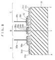
- Fig. 5 shows a MIS-type electroluminescent device 60 having a high-resistance layer formed on a light-emitting layer. More specifically, the device 60 comprises an insulating ZnS substrate 61, a device body formed on the substrate and having an n-type ZnS conductive layer 62 and an n-type ZnS light-emitting layer 63 on the layer 62, a ZnS high-resistance layer 64 formed on the light-emitting layer 63, an Au positive electrode 65 provided on the layer 64, and an In negative electrode 66 provided on the conductive layer 62. Indicated at 65a and 66a are lead wires.
- Fig. 6 shows an electroluminescent device 90 of the p-n junction type.
- the device 90 comprises an insulating ZnSe substrate 91, a device body formed on the illustrate and comprising an n-type ZnSe conductive layer 92, an n-type ZnSe light-emitting layer 93, a p-type ZnSe light-emitting layer 94 and a p-type ZnSe conductive layer 95 which are formed one over another, an Au positive electrode 96 provided on the conductive layer 95, and an In negative electrode 97 provided on the conductive layer 92. Indicated at 96a and 97a are lead wires.
- the electrodes 66, 65 or 97, 96 are arranged respectively in an electrode forming space on the conductive layer and on the uppermost layer of the device body (on the conductive layer 55 in Fig. 9, On the high-resistance layer 64 in Fig. 5, or on the conductive layer 95 in Fig. 6) for applying a voltage therethrough to the device body.
- the voltage which would otherwise be applied via the substrate can be efficiently applied to the device body. This precludes the loss due to the substrate to result in the following advantages.
- Such a compound semiconductor electroluminescent device is fabricated by placing a mask having a specified rectangular aperture on a high-resistance compound semiconductor substrate, for example, of 106 to 1015 ohm-cm, forming a low-resistance semiconductor conductive layer as the lowermost layer first on the substrate, and forming a compound semiconductor light-emitting layer, and a compound semiconductor high-resistance layer or a compound semiconductor conductive layer as superposed layers on the resulting conductive layer except at an electrode forming site.
- the layers are formed, for example, by MBE.
- the device is prepared in this way by one of the following two processes.
- the first of the processes comprises placing a mask of thin metal film having at least one specified rectangular aperture on the compound semiconductor substrate, epitaxially growing a compound semiconductor conductive layer first as the lowermost layer, the shifting the mask so as to cover the electrode forming site on the layer with the mask, forming a compound semiconductor light-emitting layer on the conductive layer, further epitaxially growing a compound semiconductor high-resistance layer or compound semiconductor conductive layer on the light-emitting layer to obtain a device body, removing the mask and thereafter providing electrodes at the electrode forming site on the lowermost conductive layer and on the surface of the uppermost high-resistance layer or conductive layer.
- the second process comprises placing a mask of thin metal film having at least one specified rectangular aperture over the compound semiconductor substrate at a specified distance (which is usually 10 to 500 ⁇ m to be suitable) away therefrom, epitaxially growing a compound semiconductor conductive layer first, then altering the angle of inclination of the substrate provided with the mask (generally suitably by 5 to 45 degrees) with respect to the direction of projection of the molecular beam to mask an electrode forming site on the conductive layer, forming a compound semiconductor light emitting layer on the conductive layer, further epitaxially growing a compound semiconductor high-resistance layer or compound semiconductor conductive layer on the resulting layer to obtain a device body, removing the mask and providing electrodes at the electrode forming site on the lowermost conductive layer and on the surface of the uppermost high-resistance layer or conductive layer.
- the electroluminescent device body thus obtained comprises epitaxial compound semiconductor layers which are all identical in shape when seen from above. It is suitable that the electrode forming site on the lowermost layer be usually 5 to 80% of the surface of the lowermost layer in area.
- Figs. 7 and 8 show a ZnS multicolor electroluminescent device of the MIS type similar to the one shown in Fig. 5.
- the device comprises a semi-insulating (high-resistance) ZnS substrate 31, a low resistance n-type epitaxial ZnS conductive layer 32, low-resistance n-type epitaxial ZnS light emitting layers 33a, 33b, 33c, hole injecting epitaxial ZnS high resistance layers 34a, 34b, 34c, an ohmic metal (In) electrode 35 formed on the conductive layer 32, metal (Au) electrodes 36a, 36b, 36c formed on the respective high resistance layers 34a, 34b, 34c, and metal lead wires 37, 38a, 38b, 38c.
- This device is prepared by placing a mask of thin metal plate having a rectangular aperture on the semi-insulating (high-resistance) ZnS substrate 31, growing the conductive layer 32 by MBE, thereafter growing the light-emitting layer 33a and the high-resistance layer 34a in overlapping relation with the conductive layer 32 by MBE with the mask shifted to form a light emitting portion A, similarly forming light-emitting portions B and C in succession with the mask further shifted, and providing the electrodes 35, 36a, 36b and 36c.
- the device thus formed includes the three light-emitting portions A, B and C having the conductive layer 32 in common.
- the light-emitting layers of the respective light-emitting portions have added thereto as impurities Al and Ag at about one-tenth the concentration of Al, Al and Cu at about one-tenth the concentration of Al, and Al and cadmium (Cd) at one-half the concentration of Al, respectively.
- Fig. 1 is a diagram showing an electroluminescent device as a first embodiment of the invention.
- Indicated at 1a is an n-type ZnSe substrate having a resistivity of about 1 ohm-cm prepared from a ZnSe bulk single crystal grown by the halogen chemical transport process, by heat-treating the crystal in molten zinc at 1000°C for 100 hours to reduce the resistance.
- a mask having a circular aperture with a diameter of 30 to 100 ⁇ m is placed on the substrate 1a, and layers are epitaxially formed one over another on the substrate by MBE.
- These layers are a conductive layer 53 of low-resistance n-type ZnSe having an impurity concentration of at least 1018 cm ⁇ 3, a light-emitting layer 42 of n-type ZnSe having an impurity concentration of about 5 x 1016 cm ⁇ 3, and a hole injecting insulating layer 144 of insulating ZnSe.
- a positive electrode 7 is then formed by depositing gold (Au).
- the substrate is disposed perpendicular to the direction of incidence of the beam for each starting material, whereby the device body can be grown in the form of a solid cylinder, 30 to 100 ⁇ m in diameter, with good controllability locally at the position on the substrate corresponding to the circular aperture in the mask.
- an insulating layer 115 of insulating ZnSe is epitaxially grown. This layer is grown over the side surface and top face of the cylindrical device body to a large thickness while rotating the substrate as inclined with respect to the direction of incidence of each molecular beam.
- the excessive insulating ZnSe deposited on the positive electrode 7 is removed as by chemical etching, and an annular ohmic electrode of In serving as a negative electrode 8 is formed on the rear surface of the substrate la to complete a MIS-type electroluminescent device.
- the present embodiment With the present embodiment, current through the device is confined to the solid cylindrical device body and can be injected into the light emitting layer at a high density.
- the embodiment thus realizes a ZnSe MIS-type electroluminescent device of high brightness.
- the semiconductors for forming the substrate and the electroluminescent device body are each ZnS or zinc sulfo-selenide (ZnS x Se 1-x ).
- the MIS-type device of this embodiment also produces light with high brightness.
- Fig. 2 is a diagram showing a third embodiment of the invention.
- epitaxially formed on the same low-resistance ZnSe substrate 1a as used in the first embodiment are a conductive layer 53 made of n-type ZnSe and having an impurity concentration of 1018 cm ⁇ 3, a light-emitting layer 24 made of n-type ZnSe and having an impurity concentration of 1017 cm ⁇ 3, and a light-emitting layer 25 made of p-type ZnSe and having a hole concentration of 1016 cm ⁇ 3
- MOCVD or MBE a conductive layer 53 made of n-type ZnSe and having an impurity concentration of 1018 cm ⁇ 3
- a light-emitting layer 24 made of n-type ZnSe and having an impurity concentration of 1017 cm ⁇ 3
- a light-emitting layer 25 made of p-type ZnSe and having a hole concentration of 1016 cm ⁇ 3
- the grown layer block and the substrate are partially etched away, for example, by chemical etching or reactive ion beam etching to form an electroluminescent device body in the form of a solid cylinder, 50 ⁇ m in diameter.
- Insulating ZnS x Se 1-x is thereafter grown epitaxially over the device body to form an insulating layer 125.
- the insulating ZnS x Se 1-x is controlled to a sulfur content (x) of about 0.3 to 0.7 so as to have a sufficiently lower refractive index than the ZnSe forming the device body including the light-emitting layers 24, 25, with the difference in lattice constant therebetween diminished.
- the insulating ZnS x Se 1-x portion formed over the light-emitting layer 25 is etched away, and an ohmic electrode of Au is formed over the exposed layer 25 to provide a positive electrode 7.
- An ohmic electrode of In is formed on the rear surface of the substrate 1a to provide a negative electrode 8. Consequently, a p-n junction electroluminescent device is obtained.
- the present embodiment is adapted to permit current to flow into the light-emitting layers 24, 25 at an increased density, while the insulating layer 125 is lower in refractive index than the device body including the light-emitting layers 24, 25, with the result that the light produced by these layers 24, 25 is confined in the device body and can be delivered through the substrate.
- the ZnSe p-n junction device fabricated produces light with high brightness and high delivery efficiency.
- the Group II - VI compound semiconductor for forming the substrate and the device body is ZnS x Se 1-x (0.5 > x > 0), and the insulating layer is formed of ZnS z Se 1-z having about 0.5 higher sulfur content (z) than the ZnS x Se 1-x .
- this embodiment i.e. ZnS x Se 1-x p-n junction electroluminescent device, exhibits high brightness and achieves a high delivery efficiency.
- Fig. 3 is a diagram showing a fifth embodiment of the invention.
- an n-type ZnS x Se 1-x substrate 121 having a resistivity of about 1 ohm-cm is prepared from a ZnS x Se 1-x bulk single crystal grown by the halogen chemical transport process, by heat-treating the crystal in molten zinc at 1000° C for 100 hours to reduce the resistance.
- the layer block obtained is etched to form an electroluminescent device body in the form of a solid cylinder.
- insulating ZnS y Se 1-y is epitaxially grown over the device body in the same manner as in the first and third embodiments to form an insulating layer 135 surrounding the device body, followed by formation of a positive electrode 7 of Au and a negative electrode 8 of In to fabricate a p-n junction electro luminescent device.
- the sulfur content (x) of ZnS x Se 1-x for forming the n-type and p-type conductive layers 63, 27 is adjusted to about 0.1 so that the semiconductor is about 0.1 eV greater than the ZnSe forming the emitting layers 24, 25 in band gap.
- the sulfur content (y) of ZnS y Se 1-y for forming the insulating layer 135 is adjusted to about 0.3 to about 0.7 so that the layer has a sufficiently lower refractive index than the device body, with a diminished lattice constant difference therebetween.
- the present embodiment is adapted to confine the current and light, while the light-emitting layers 24, 25 of ZnSe are sandwiched between the conductive layers 63, 27 of ZnS x Se 1-x having a greater band gap than ZnSe to confine the carrier to the light-emitting layers. This ensures a high luminescence efficiency.
- the ZnSe p-n junction electroluminescent device thus realized therefore exhibits high brightness and high efficiency.
- the light-emitting layers are prepared from ZnS z Se 1-z with a sulfur content (z) of up to 0.5, and the sulfur content of the semiconductors for the conductive layer and the insulating layer is made greater by the value z.
- this embodiment realizes a ZnSSe p-n junction electroluminescent device exhibiting high brightness and high efficiency.
- Fig. 4 is a diagram showing a seventh embodiment of the invention.
- an insulating ZnSe substrate prepared from a ZnSe bulk single crystal grown by the halogen chemical transport process without subjecting the crystal to low-resistance treatment.
- an n-type ZnSe conductive layer 53, an n-type ZnSe light-emitting layer 24 and p-type ZnSe light-emitting layer 25 are epitaxially grown one over another on the insulating ZnSe substrate 21.
- the grown layer block is then shaped into a column by etching the block until the n-type ZnSe conductive layer 53 is exposed.
- the layer block is further shaped into the columnar form along with a portion of the substrate 1a with the conductive layer 53 locally left unetched to obtain a columnar electroluminescent device body and a negative electrode forming portion 53a of the layer 53 extending from the body in the form of a tongue.
- Insulating ZnS x Se 1-x having a sulfur content (x) of about 0.3 to about 0.7 is further grown over the resulting product to form an insulating layer 135.
- the insulating ZnS x Se 1-x portion deposited on the light-emitting layer 25 and the tonguelike portion 53a of the layer 53 is etched away.
- An Au positive electrode 7 and an In negative electrode 8 are then formed on the exposed surfaces of the light-emitting layer 25 and the tongue-like portion 53a, respectively, whereby a planar p-n junction electroluminescent device is obtained.
- the ZnSe p-n junction electroluminescent device fabricated according to this embodiment is of the planar type and exhibits high brightness and high delivery efficiency.
- ZnS x Se 1-x is used as the semiconductor for the device body, and the insulating layer 135 is prepared from ZnS z Se 1-z (x ⁇ z) having a higher sulfur content than the above ZnS x Se 1-x .
- this embodiment realizes a planar p-n junction electroluminescent device exhibiting high brightness and high delivery efficiency.
- the first to eighth embodiments realize compound semiconductor electroluminescent devices which luminesce over the range of ultraviolet rays to visible rays including blue rays with high brightness and high delivery efficiency and which are therefore very useful as high-energy and high-brightness light sources for use in various displays, printers, facsimile systems, etc.
Landscapes
- Engineering & Computer Science (AREA)
- Physics & Mathematics (AREA)
- General Physics & Mathematics (AREA)
- Theoretical Computer Science (AREA)
- Manufacturing & Machinery (AREA)
- Computer Hardware Design (AREA)
- Microelectronics & Electronic Packaging (AREA)
- Power Engineering (AREA)
- Led Devices (AREA)
- Electroluminescent Light Sources (AREA)
- Physical Deposition Of Substances That Are Components Of Semiconductor Devices (AREA)
- Semiconductor Lasers (AREA)
Claims (18)
- Composant électroluminescent en un semiconducteur composé du groupe II-VI, qui comprend
un corps de composant électroluminescent formé sur un substrat (1a) et définissant une région émettrice de lumière (42) et une région conductrice (53) qui est disposée au moins entre le substrat et la région émettrice de lumière (42), et
un couple d'électrodes (7, 8) formé sur le corps du composant électroluminescent ou à la fois sur le corps du composant électroluminescent et sur le substrat (1a) pour appliquer une tension externe au corps, afin de provoquer une électroluminescence,
la région émettrice de lumière (42) et la région conductrice (53) étant formées chacune en un semiconducteur composé du groupe II-VI et réalisées chacune de manière à présenter une résistance très faible par l'adjonction d'éléments d'impuretés identiques ou différents pour les deux régions,
le corps du composant ayant sensiblement la forme d'une colonne dressée sur le substrat (1a) et entourée par une région isolante (115) sur la totalité de sa surface latérale, et
la région isolante (115) étant formée en un semiconducteur composé du groupe II-VI et ayant un indice de réfraction équivalent ou inférieur à celui de la région émettrice de lumière (42) et/ou à celui de la région conductrice (53). - Composant tel que défini dans la revendication 1, dans lequel le semiconducteur composé du groupe II-VI, qui forme chacune des régions conductrice et émettrice de lumière, est du ZnS, du ZnSe ou du ZnSxSe1-x.
- Composant tel que défini dans la revendication 1, dans lequel le semiconducteur composé du groupe II-VI, qui forme la région isolante, est du ZnS, du ZnSe ou du ZnSySe1-y.
- Composant tel que défini dans la revendication 1, dans lequel le semiconducteur composé du groupe II-VI, qui forme chacune des régions conductrice et émettrice de lumière, est du ZnSe, et le semiconducteur composé du groupe II-VI, qui forme la région isolante, est du ZnSe ou du ZnSySe1-y, avec 0,3<y<0,7.
- Composant tel que défini dans la revendication 1, dans lequel le semiconducteur composé du groupe II-VI formant la région conductrice est du ZnSxSe1-x, avec 0,5>x>0, le semiconducteur composé du groupe II-VI formant la région émettrice de lumière est du ZnSe, et le semiconducteur composé du groupe II-VI formant la région isolante est du ZnSySe1-y, avec y>x+0,5.
- Composant tel que défini dans la revendication 1, dans lequel le semiconducteur composé du groupe II-VI formant la région conductrice est du ZnSxSe1-x, avec x = O,1, le semiconducteur composé du groupe II-VI formant la région isolante est du ZnSySe1-y, avec 0,3<y<0,7, et le semiconducteur composé du groupe II-VI formant la région émettrice de lumière est du ZnSe présentant une bande interdite plus petite que celle du ZnSxSe1-x de la région conductrice.
- Composant tel que défini dans la revendication 1, dans lequel le substrat est constitué d'un ZnS, ZnSe ou ZnSzSe1-z conducteur.
- Composant tel que défini dans la revendication 1, dans lequel le substrat est constitué d'un ZnS, ZnSe ou ZnSzSe1-z isolant.
- Composant tel que défini dans la revendication 1, dans lequel la région isolante est constituée d'un CaS, CaSe, SrS ou SrSe isolant.
- Composant tel que défini dans la revendication 1, dans lequel la région isolante comporte une paroi qui entoure le corps du composant et présente une épaisseur de 2 à 10 µ.
- Composant tel que défini dans la revendication 1, dans lequel la région émettrice de lumière est une couche luminescente du type MIS (métal-isolant-semiconducteur), formée de ZnS ou ZnSe auquel un élément d'impureté a été ajouté.
- Composant tel que défini dans la revendication 1, dans lequel la région émettrice de lumière est une couche luminescente de structure planar présentant une jonction PN formée par la combinaison de ZnS auquel un élément d'impureté du type P a été ajouté, ledit élément d'impureté du type P étant un élément du groupe I ou V, ou une combinaison d'éléments des groupes I et V, et de ZnS auquel un élément d'impureté du type N a été ajouté, ledit élément d'impureté du type N étant un élément du groupe III ou VII, ou une combinaison d'éléments des groupes III et VII.
- Composant tel que défini dans la revendication 1, dans lequel la région émettrice de lumière est une couche luminescente de structure planar présentant une jonction PN formée par la combinaison de ZnSe auquel un élément d'impureté du type P a été ajouté, ledit élément d'impureté du type P étant un élément du groupe I ou V, ou une combinaison d'éléments des groupes I et V, et de ZnSe auquel un élément d'impureté du type N a été ajouté, ledit élément d'impureté du type N étant un élément du groupe III ou VII, ou une combinaison d'éléments des groupes III et VII.
- Composant tel que défini dans la revendication 1, dans lequel la région émettrice de lumière est une couche luminescente du type MIS formée de ZnShSe1-h, avec 0,5>h>o, auquel un élément d'impureté du type N a été ajouté, ledit élément d'impureté du type N est un élément du groupe III ou VII, ou une combinaison d'éléments des groupes III et VII, et la région isolante est formée de ZnSySe1-y, avec y>h+0,5, auquel aucun élément d'impureté n'a été ajouté.
- Composant tel que défini dans la revendication 1, dans lequel la région conductrice et la région émettrice de lumière sont, vues en plan, de formes identiques, et la couche conductrice est formée sur le substrat, la région émettrice de lumière étant formée sur la couche conductrice et sur le substrat, avec un espace réservé localement, pour la formation d'une électrode, sur la surface supérieure de la couche conductrice, les deux électrodes étant reliées respectivement à la couche conductrice et à la région émettrice de lumière.
- Composant tel que défini dans la revendication 1, dans lequel l'une des électrodes est reliée au corps du composant, et la seconde électrode est reliée à une surface du substrat opposée à l'autre surface de ce dernier, sur laquelle le corps du composant est formé.
- Composant tel que défini dans la revendication 13 ou 15, dans lequel le substrat est formé de ZnSe isolant, et le corps du composant comprend une couche conductrice en ZnSe à laquelle un élément d'impureté du type N a été ajouté, une couche émettrice de lumière en ZnSe à laquelle un élément d'impureté du type N a été ajouté, et une couche émettrice de lumière en ZnSe à laquelle un élément d'impureté du type P a été ajouté, les couches constitutives du corps du composant étant formées sur le substrat, au moins sur la totalité de la surface de sa partie centrale, et superposées l'une à l'autre dans l'ordre mentionné, la région isolante entourant le corps du composant sur la totalité de la surface latérale de ce dernier à l'exception d'une partie d'extrémité de la couche conductrice en ZnSe, l'une des électrodes étant faite d'In et disposée sur ladite partie d'extrémité de la couche conductrice en ZnSe, la seconde électrode étant faite d'Au et disposée sur la couche émettrice de lumière en ZnSe du type P.
- Composant tel que défini dans la revendication 11 ou 16, dans lequel le substrat est un substrat en ZnSe auquel un élément d'impureté du type N a été ajouté, et le corps du composant comprend une couche conductrice en ZnSe à laquelle un élément d'impureté du type N a été ajouté, une couche émettrice de lumière en ZnSe à laquelle un élément d'impureté du type N a été ajouté, et une couche d'injection de trous en ZnSe isolant, les couches constitutives du corps du composant étant formées sur le substrat, en couvrant la totalité de la surface de sa partie centrale, et superposées l'une à l'autre dans l'ordre mentionné, la région isolante entourant la totalité de la surface latérale du corps du composant, l'une des électrodes étant faite d'Au et disposée sur la couche d'injection de trous, la seconde électrode étant faite d'In et disposée sur une surface du substrat opposée à l'autre surface de ce dernier, sur laquelle le corps du composant est formé.
Applications Claiming Priority (4)
| Application Number | Priority Date | Filing Date | Title |
|---|---|---|---|
| JP18266488A JP2708183B2 (ja) | 1988-07-21 | 1988-07-21 | 化合物半導体発光素子 |
| JP182664/88 | 1988-07-21 | ||
| JP63240556A JPH0287685A (ja) | 1988-07-21 | 1988-09-26 | 化合物半導体発光素子 |
| JP240556/88 | 1988-09-26 |
Publications (3)
| Publication Number | Publication Date |
|---|---|
| EP0351868A2 EP0351868A2 (fr) | 1990-01-24 |
| EP0351868A3 EP0351868A3 (fr) | 1991-10-16 |
| EP0351868B1 true EP0351868B1 (fr) | 1994-09-21 |
Family
ID=26501383
Family Applications (3)
| Application Number | Title | Priority Date | Filing Date |
|---|---|---|---|
| EP89113443A Expired - Lifetime EP0351869B1 (fr) | 1988-07-21 | 1989-07-21 | Dispositif électroluminescent à semi-conducteur composé |
| EP89113441A Expired - Lifetime EP0351867B1 (fr) | 1988-07-21 | 1989-07-21 | Dispositif électroluminescent à semi-conducteur composé |
| EP89113442A Expired - Lifetime EP0351868B1 (fr) | 1988-07-21 | 1989-07-21 | Dispositif électroluminescent à semi-conducteur composé |
Family Applications Before (2)
| Application Number | Title | Priority Date | Filing Date |
|---|---|---|---|
| EP89113443A Expired - Lifetime EP0351869B1 (fr) | 1988-07-21 | 1989-07-21 | Dispositif électroluminescent à semi-conducteur composé |
| EP89113441A Expired - Lifetime EP0351867B1 (fr) | 1988-07-21 | 1989-07-21 | Dispositif électroluminescent à semi-conducteur composé |
Country Status (4)
| Country | Link |
|---|---|
| US (3) | US5037709A (fr) |
| EP (3) | EP0351869B1 (fr) |
| JP (5) | JP2708183B2 (fr) |
| DE (3) | DE68918361T2 (fr) |
Families Citing this family (49)
| Publication number | Priority date | Publication date | Assignee | Title |
|---|---|---|---|---|
| JPH0268968A (ja) * | 1988-09-02 | 1990-03-08 | Sharp Corp | 化合物半導体発光素子 |
| EP0377320B1 (fr) * | 1988-12-27 | 1997-07-30 | Canon Kabushiki Kaisha | Appareil émetteur de lumière au moyen d'un champ électrique |
| JP2588280B2 (ja) * | 1989-07-10 | 1997-03-05 | シャープ株式会社 | 化合物半導体発光素子 |
| JP2593960B2 (ja) * | 1990-11-29 | 1997-03-26 | シャープ株式会社 | 化合物半導体発光素子とその製造方法 |
| US5198690A (en) * | 1990-11-26 | 1993-03-30 | Sharp Kabushiki Kaisha | Electroluminescent device of II-IV compound semiconductor |
| US5252895A (en) * | 1991-05-09 | 1993-10-12 | Westinghouse Electric Corp. | TFEL edge emitter structure with light emitting face at angle greater than ninety degrees to substrate street |
| US5291507A (en) * | 1991-05-15 | 1994-03-01 | Minnesota Mining And Manufacturing Company | Blue-green laser diode |
| US5274269A (en) * | 1991-05-15 | 1993-12-28 | Minnesota Mining And Manufacturing Company | Ohmic contact for p-type group II-IV compound semiconductors |
| CN1111840A (zh) * | 1991-05-15 | 1995-11-15 | 明尼苏达州采矿制造公司 | 蓝-绿激光二极管的制造方法 |
| US5404027A (en) * | 1991-05-15 | 1995-04-04 | Minnesota Mining & Manufacturing Compay | Buried ridge II-VI laser diode |
| US5183689A (en) * | 1991-07-15 | 1993-02-02 | Cvd, Inc. | Process for an improved laminated of znse and zns |
| JP2837004B2 (ja) * | 1991-09-30 | 1998-12-14 | 株式会社デンソー | Elディスプレイ素子 |
| JPH05182766A (ja) * | 1991-12-26 | 1993-07-23 | Toyota Central Res & Dev Lab Inc | 薄膜el素子 |
| US5536584A (en) * | 1992-01-31 | 1996-07-16 | Hitachi, Ltd. | Polyimide precursor, polyimide and metalization structure using said polyimide |
| AU4104293A (en) * | 1992-05-19 | 1993-12-13 | California Institute Of Technology | Wide band-gap semiconductor light emitters |
| WO1994015369A1 (fr) * | 1992-12-22 | 1994-07-07 | Research Corporation Technologies, Inc. | Dispositifs semi-conducteurs electroluminescents composes des groupes ii a vi et contact ohmique a cet effet |
| JPH06196261A (ja) * | 1992-12-25 | 1994-07-15 | Hitachi Maxell Ltd | 薄膜型エレクトロルミネツセンス素子 |
| US5459337A (en) * | 1993-02-19 | 1995-10-17 | Sony Corporation | Semiconductor display device with red, green and blue emission |
| US5422902A (en) * | 1993-07-02 | 1995-06-06 | Philips Electronics North America Corporation | BeTe-ZnSe graded band gap ohmic contact to p-type ZnSe semiconductors |
| US5445550A (en) * | 1993-12-22 | 1995-08-29 | Xie; Chenggang | Lateral field emitter device and method of manufacturing same |
| JP3156503B2 (ja) | 1994-05-27 | 2001-04-16 | 松下電器産業株式会社 | 固体撮像装置の駆動方法及び固体撮像装置の信号処理回路 |
| DE69425383T2 (de) * | 1994-10-11 | 2001-02-15 | International Business Machines Corp., Armonk | Monoelektrische anordnung von lichtemittierenden dioden zur lichterzeugung mehrerer wellenlängen und deren anwendung für mehrfarben-anzeigevorrichtungen |
| US5796120A (en) * | 1995-12-28 | 1998-08-18 | Georgia Tech Research Corporation | Tunnel thin film electroluminescent device |
| JP2839027B2 (ja) * | 1997-01-23 | 1998-12-16 | 住友電気工業株式会社 | Ii−vi族化合物半導体の熱処理方法 |
| JP3934730B2 (ja) * | 1997-03-28 | 2007-06-20 | ローム株式会社 | 半導体発光素子 |
| US5889364A (en) * | 1997-08-22 | 1999-03-30 | Durel Corporation | Electrical, solderless snap connector for EL lamp |
| JP2001267085A (ja) * | 2000-03-23 | 2001-09-28 | Sanyo Electric Co Ltd | 有機発光装置およびその製造方法 |
| US7064355B2 (en) * | 2000-09-12 | 2006-06-20 | Lumileds Lighting U.S., Llc | Light emitting diodes with improved light extraction efficiency |
| JP2002141556A (ja) * | 2000-09-12 | 2002-05-17 | Lumileds Lighting Us Llc | 改良された光抽出効果を有する発光ダイオード |
| US7053419B1 (en) | 2000-09-12 | 2006-05-30 | Lumileds Lighting U.S., Llc | Light emitting diodes with improved light extraction efficiency |
| US6650044B1 (en) * | 2000-10-13 | 2003-11-18 | Lumileds Lighting U.S., Llc | Stenciling phosphor layers on light emitting diodes |
| DE10051159C2 (de) * | 2000-10-16 | 2002-09-19 | Osram Opto Semiconductors Gmbh | LED-Modul, z.B. Weißlichtquelle |
| US6987613B2 (en) * | 2001-03-30 | 2006-01-17 | Lumileds Lighting U.S., Llc | Forming an optical element on the surface of a light emitting device for improved light extraction |
| DE10120703A1 (de) * | 2001-04-27 | 2002-10-31 | Osram Opto Semiconductors Gmbh | Halbleiterchip für die Optoelektronik |
| JP3758562B2 (ja) * | 2001-11-27 | 2006-03-22 | 日亜化学工業株式会社 | 窒化物半導体多色発光素子 |
| JP2005026688A (ja) * | 2003-06-30 | 2005-01-27 | Osram Opto Semiconductors Gmbh | 放射放出半導体チップ、該半導体チップの作製方法および該半導体チップの明るさの調整設定方法 |
| US7009213B2 (en) * | 2003-07-31 | 2006-03-07 | Lumileds Lighting U.S., Llc | Light emitting devices with improved light extraction efficiency |
| US7151338B2 (en) * | 2003-10-02 | 2006-12-19 | Hewlett-Packard Development Company, L.P. | Inorganic electroluminescent device with controlled hole and electron injection |
| JP2005123526A (ja) * | 2003-10-20 | 2005-05-12 | Oki Data Corp | 半導体装置、ledヘッド、及び画像形成装置 |
| DE102004029412A1 (de) * | 2004-02-27 | 2005-10-13 | Osram Opto Semiconductors Gmbh | Strahlungsemittierender Halbleiterchip und Verfahren zur Herstellung eines solchen Halbleiterchips |
| US7462502B2 (en) | 2004-11-12 | 2008-12-09 | Philips Lumileds Lighting Company, Llc | Color control by alteration of wavelength converting element |
| US7419839B2 (en) * | 2004-11-12 | 2008-09-02 | Philips Lumileds Lighting Company, Llc | Bonding an optical element to a light emitting device |
| WO2007091500A1 (fr) * | 2006-02-10 | 2007-08-16 | Semiconductor Energy Laboratory Co., Ltd. | Element emetteur de lumiere, dispositif emetteur de lumiere, et dispositif electronique |
| JP5300345B2 (ja) | 2007-08-10 | 2013-09-25 | キヤノン株式会社 | 発光膜、発光素子およびその製造方法 |
| US9337407B2 (en) * | 2009-03-31 | 2016-05-10 | Epistar Corporation | Photoelectronic element and the manufacturing method thereof |
| KR100986440B1 (ko) * | 2009-04-28 | 2010-10-08 | 엘지이노텍 주식회사 | 발광소자 및 그 제조방법 |
| US20120097918A1 (en) * | 2010-10-20 | 2012-04-26 | Varian Semiconductor Equipment Associates, Inc. | Implanted current confinement structure to improve current spreading |
| WO2015097595A1 (fr) * | 2013-12-27 | 2015-07-02 | Semiconductor Energy Laboratory Co., Ltd. | Dispositif électroluminescent |
| CN109346497A (zh) * | 2018-09-26 | 2019-02-15 | 北京蜃景光电科技有限公司 | 微显示器件及其制备方法、显示面板 |
Family Cites Families (23)
| Publication number | Priority date | Publication date | Assignee | Title |
|---|---|---|---|---|
| US3919589A (en) * | 1973-04-06 | 1975-11-11 | Rca Corp | Electroluminescent cell with a current-limiting layer of high resistivity |
| JPS5437800B2 (fr) * | 1973-06-19 | 1979-11-16 | ||
| JPS5444547Y2 (fr) * | 1975-02-27 | 1979-12-21 | ||
| US3991339A (en) * | 1975-05-27 | 1976-11-09 | Rca Corporation | Light emitting diode with reflector |
| US4025157A (en) * | 1975-06-26 | 1977-05-24 | The United States Of America As Represented By The Secretary Of The Navy | Gradient index miniature coupling lens |
| JPS5643783A (en) * | 1979-09-18 | 1981-04-22 | Toshiba Corp | Light emitting diode for optical communication |
| JPS58128784A (ja) * | 1982-01-27 | 1983-08-01 | Nippon Telegr & Teleph Corp <Ntt> | 半導体発光装置 |
| JPS58137271A (ja) * | 1982-02-10 | 1983-08-15 | Toshiba Corp | 光半導体素子用レンズ、光半導体素子用レンズの製造方法、及び光半導体素子 |
| US4634934A (en) * | 1982-05-19 | 1987-01-06 | Matsushita Electric Industrial Co. Ltd. | Electroluminescent display device |
| JPS58218180A (ja) * | 1982-06-11 | 1983-12-19 | Toshiba Corp | 半導体発光素子およびその製造方法 |
| US4706254A (en) * | 1983-05-12 | 1987-11-10 | Canon Kabushiki Kaisha | Semiconductor device and its fabrication |
| JPS6085585A (ja) * | 1983-10-17 | 1985-05-15 | Nec Corp | 埋め込み型半導体レ−ザ |
| JPS59188182A (ja) * | 1984-03-23 | 1984-10-25 | Hitachi Ltd | 発光半導体装置 |
| JPS617050U (ja) * | 1984-06-18 | 1986-01-16 | 三洋電機株式会社 | Mis型発光ダイオ−ド |
| CA1251549A (fr) * | 1984-07-24 | 1989-03-21 | Akira Suzuki | Dispositif semiconducteur luminescent |
| JPS6199392A (ja) * | 1984-10-19 | 1986-05-17 | Sanyo Electric Co Ltd | Mis型発光ダイオ−ド |
| JPH0750795B2 (ja) * | 1985-03-28 | 1995-05-31 | キヤノン株式会社 | 発光素子 |
| JPH06101590B2 (ja) * | 1985-05-01 | 1994-12-12 | セイコーエプソン株式会社 | 青色発光素子及びその製造法 |
| JPS61258483A (ja) * | 1985-05-11 | 1986-11-15 | Oki Electric Ind Co Ltd | 半導体面発光素子 |
| JPH0697704B2 (ja) * | 1986-01-27 | 1994-11-30 | シャープ株式会社 | MIS型ZnS青色発光素子 |
| JPS639165A (ja) * | 1986-06-30 | 1988-01-14 | Matsushita Electric Ind Co Ltd | 発光ダイオ−ド |
| JP2723227B2 (ja) * | 1986-09-26 | 1998-03-09 | 株式会社東芝 | 半導体発光素子の製造方法 |
| JP2521675B2 (ja) * | 1986-10-03 | 1996-08-07 | 株式会社小松製作所 | レ−ザ装置 |
-
1988
- 1988-07-21 JP JP18266488A patent/JP2708183B2/ja not_active Expired - Fee Related
- 1988-09-26 JP JP63240556A patent/JPH0287685A/ja active Pending
-
1989
- 1989-07-19 US US07/382,238 patent/US5037709A/en not_active Expired - Lifetime
- 1989-07-19 US US07/382,239 patent/US5055363A/en not_active Expired - Lifetime
- 1989-07-19 US US07/382,237 patent/US4988579A/en not_active Expired - Lifetime
- 1989-07-21 DE DE68918361T patent/DE68918361T2/de not_active Expired - Fee Related
- 1989-07-21 EP EP89113443A patent/EP0351869B1/fr not_active Expired - Lifetime
- 1989-07-21 EP EP89113441A patent/EP0351867B1/fr not_active Expired - Lifetime
- 1989-07-21 DE DE68919291T patent/DE68919291T2/de not_active Expired - Fee Related
- 1989-07-21 EP EP89113442A patent/EP0351868B1/fr not_active Expired - Lifetime
- 1989-07-21 DE DE68918362T patent/DE68918362T2/de not_active Expired - Fee Related
-
1997
- 1997-06-16 JP JP15832597A patent/JP3069533B2/ja not_active Expired - Lifetime
- 1997-06-16 JP JP15832497A patent/JP3066344B2/ja not_active Expired - Fee Related
-
1998
- 1998-11-24 JP JP10332248A patent/JPH11220175A/ja active Pending
Also Published As
| Publication number | Publication date |
|---|---|
| DE68918361D1 (de) | 1994-10-27 |
| JPH1056205A (ja) | 1998-02-24 |
| US5055363A (en) | 1991-10-08 |
| JPH0232570A (ja) | 1990-02-02 |
| EP0351869B1 (fr) | 1994-11-09 |
| DE68918361T2 (de) | 1995-03-30 |
| EP0351869A2 (fr) | 1990-01-24 |
| EP0351867B1 (fr) | 1994-09-21 |
| DE68919291D1 (de) | 1994-12-15 |
| US4988579A (en) | 1991-01-29 |
| EP0351868A2 (fr) | 1990-01-24 |
| EP0351869A3 (fr) | 1991-10-16 |
| EP0351867A2 (fr) | 1990-01-24 |
| JP2708183B2 (ja) | 1998-02-04 |
| JPH11220175A (ja) | 1999-08-10 |
| JP3069533B2 (ja) | 2000-07-24 |
| US5037709A (en) | 1991-08-06 |
| EP0351867A3 (fr) | 1991-10-16 |
| JPH0287685A (ja) | 1990-03-28 |
| EP0351868A3 (fr) | 1991-10-16 |
| DE68918362D1 (de) | 1994-10-27 |
| DE68918362T2 (de) | 1995-01-19 |
| JPH1056204A (ja) | 1998-02-24 |
| JP3066344B2 (ja) | 2000-07-17 |
| DE68919291T2 (de) | 1995-03-23 |
Similar Documents
| Publication | Publication Date | Title |
|---|---|---|
| EP0351868B1 (fr) | Dispositif électroluminescent à semi-conducteur composé | |
| JPH0268968A (ja) | 化合物半導体発光素子 | |
| KR20000037764A (ko) | 발광다이오드 및 그 제조방법 | |
| US4916496A (en) | ZnS blue light emitting device | |
| US5554877A (en) | Compound semiconductor electroluminescent device | |
| JPH11233816A (ja) | 半導体発光装置およびその製造方法 | |
| US5032539A (en) | Method of manufacturing green light emitting diode | |
| JPH03268360A (ja) | 半導体装置 | |
| US7355213B2 (en) | Electrode material and semiconductor element | |
| US4040074A (en) | Semiconductor cold electron emission device | |
| JPH10107321A (ja) | 半導体素子の電極形成方法 | |
| JPS6351552B2 (fr) | ||
| JPS6351553B2 (fr) | ||
| JPS63116475A (ja) | Ledアレイ及びその製造法 | |
| JPS62211971A (ja) | 半導体発光装置 | |
| JPH01296687A (ja) | 可視発光半導体レーザ装置 | |
| JPH0637356A (ja) | 発光素子 | |
| JP2003046120A (ja) | 発光素子用積層構造体、発光素子、ランプ及び光源 | |
| US20050227404A1 (en) | Manufacture of a semiconductor light-emitting device | |
| JPH0590639A (ja) | 半導体発光素子の製造方法 | |
| JPS592382A (ja) | 半導体発光装置 | |
| JPS59201476A (ja) | 半導体発光装置 | |
| JPS60143680A (ja) | Mis型発光ダイオ−ド | |
| JPH09232634A (ja) | 発光ダイオードアレイ | |
| JPS61268023A (ja) | 半導体素子の製造方法 |
Legal Events
| Date | Code | Title | Description |
|---|---|---|---|
| PUAI | Public reference made under article 153(3) epc to a published international application that has entered the european phase |
Free format text: ORIGINAL CODE: 0009012 |
|
| AK | Designated contracting states |
Kind code of ref document: A2 Designated state(s): DE FR GB |
|
| PUAL | Search report despatched |
Free format text: ORIGINAL CODE: 0009013 |
|
| AK | Designated contracting states |
Kind code of ref document: A3 Designated state(s): DE FR GB |
|
| 17P | Request for examination filed |
Effective date: 19920316 |
|
| 17Q | First examination report despatched |
Effective date: 19930419 |
|
| GRAA | (expected) grant |
Free format text: ORIGINAL CODE: 0009210 |
|
| AK | Designated contracting states |
Kind code of ref document: B1 Designated state(s): DE FR GB |
|
| REF | Corresponds to: |
Ref document number: 68918362 Country of ref document: DE Date of ref document: 19941027 |
|
| ET | Fr: translation filed | ||
| PLBE | No opposition filed within time limit |
Free format text: ORIGINAL CODE: 0009261 |
|
| STAA | Information on the status of an ep patent application or granted ep patent |
Free format text: STATUS: NO OPPOSITION FILED WITHIN TIME LIMIT |
|
| 26N | No opposition filed | ||
| REG | Reference to a national code |
Ref country code: GB Ref legal event code: IF02 |
|
| PGFP | Annual fee paid to national office [announced via postgrant information from national office to epo] |
Ref country code: FR Payment date: 20020709 Year of fee payment: 14 |
|
| PGFP | Annual fee paid to national office [announced via postgrant information from national office to epo] |
Ref country code: GB Payment date: 20020717 Year of fee payment: 14 |
|
| PGFP | Annual fee paid to national office [announced via postgrant information from national office to epo] |
Ref country code: DE Payment date: 20020724 Year of fee payment: 14 |
|
| PG25 | Lapsed in a contracting state [announced via postgrant information from national office to epo] |
Ref country code: GB Free format text: LAPSE BECAUSE OF NON-PAYMENT OF DUE FEES Effective date: 20030721 |
|
| PG25 | Lapsed in a contracting state [announced via postgrant information from national office to epo] |
Ref country code: DE Free format text: LAPSE BECAUSE OF NON-PAYMENT OF DUE FEES Effective date: 20040203 |
|
| GBPC | Gb: european patent ceased through non-payment of renewal fee |
Effective date: 20030721 |
|
| PG25 | Lapsed in a contracting state [announced via postgrant information from national office to epo] |
Ref country code: FR Free format text: LAPSE BECAUSE OF NON-PAYMENT OF DUE FEES Effective date: 20040331 |
|
| REG | Reference to a national code |
Ref country code: FR Ref legal event code: ST |