EP0347801B1 - Optisches Aufzeichnungsmedium und Systeme zur Informationsaufzeichnung und Wiedergabe - Google Patents
Optisches Aufzeichnungsmedium und Systeme zur Informationsaufzeichnung und Wiedergabe Download PDFInfo
- Publication number
- EP0347801B1 EP0347801B1 EP89111107A EP89111107A EP0347801B1 EP 0347801 B1 EP0347801 B1 EP 0347801B1 EP 89111107 A EP89111107 A EP 89111107A EP 89111107 A EP89111107 A EP 89111107A EP 0347801 B1 EP0347801 B1 EP 0347801B1
- Authority
- EP
- European Patent Office
- Prior art keywords
- film
- recording
- thickness
- dielectric film
- metal reflection
- Prior art date
- Legal status (The legal status is an assumption and is not a legal conclusion. Google has not performed a legal analysis and makes no representation as to the accuracy of the status listed.)
- Expired - Lifetime
Links
- 230000003287 optical effect Effects 0.000 title claims description 100
- 238000002310 reflectometry Methods 0.000 claims description 83
- 229910052751 metal Inorganic materials 0.000 claims description 78
- 239000002184 metal Substances 0.000 claims description 78
- 239000000758 substrate Substances 0.000 claims description 65
- 238000000034 method Methods 0.000 claims description 39
- 230000008018 melting Effects 0.000 claims description 26
- 238000002844 melting Methods 0.000 claims description 26
- 229910052737 gold Inorganic materials 0.000 claims description 25
- 239000000463 material Substances 0.000 claims description 23
- 230000008033 biological extinction Effects 0.000 claims description 14
- 230000008569 process Effects 0.000 claims description 12
- 230000015572 biosynthetic process Effects 0.000 claims description 11
- MCMNRKCIXSYSNV-UHFFFAOYSA-N Zirconium dioxide Chemical compound O=[Zr]=O MCMNRKCIXSYSNV-UHFFFAOYSA-N 0.000 claims description 8
- 229910052782 aluminium Inorganic materials 0.000 claims description 8
- 239000000203 mixture Substances 0.000 claims description 8
- VYPSYNLAJGMNEJ-UHFFFAOYSA-N Silicium dioxide Chemical compound O=[Si]=O VYPSYNLAJGMNEJ-UHFFFAOYSA-N 0.000 claims description 7
- GWEVSGVZZGPLCZ-UHFFFAOYSA-N Titan oxide Chemical compound O=[Ti]=O GWEVSGVZZGPLCZ-UHFFFAOYSA-N 0.000 claims description 4
- QDOXWKRWXJOMAK-UHFFFAOYSA-N dichromium trioxide Chemical compound O=[Cr]O[Cr]=O QDOXWKRWXJOMAK-UHFFFAOYSA-N 0.000 claims description 4
- 230000001678 irradiating effect Effects 0.000 claims description 4
- 230000036961 partial effect Effects 0.000 claims description 4
- ATJFFYVFTNAWJD-UHFFFAOYSA-N Tin Chemical compound [Sn] ATJFFYVFTNAWJD-UHFFFAOYSA-N 0.000 claims description 3
- 229910052681 coesite Inorganic materials 0.000 claims description 3
- 229910052906 cristobalite Inorganic materials 0.000 claims description 3
- 239000000377 silicon dioxide Substances 0.000 claims description 3
- 229910052682 stishovite Inorganic materials 0.000 claims description 3
- 229910052718 tin Inorganic materials 0.000 claims description 3
- 229910052905 tridymite Inorganic materials 0.000 claims description 3
- 229910017083 AlN Inorganic materials 0.000 claims description 2
- PIGFYZPCRLYGLF-UHFFFAOYSA-N Aluminum nitride Chemical compound [Al]#N PIGFYZPCRLYGLF-UHFFFAOYSA-N 0.000 claims description 2
- 229910000599 Cr alloy Inorganic materials 0.000 claims description 2
- 229910004541 SiN Inorganic materials 0.000 claims description 2
- 229910052950 sphalerite Inorganic materials 0.000 claims description 2
- PBCFLUZVCVVTBY-UHFFFAOYSA-N tantalum pentoxide Inorganic materials O=[Ta](=O)O[Ta](=O)=O PBCFLUZVCVVTBY-UHFFFAOYSA-N 0.000 claims description 2
- 229910052984 zinc sulfide Inorganic materials 0.000 claims description 2
- 239000010408 film Substances 0.000 description 420
- 239000010931 gold Substances 0.000 description 35
- 239000012071 phase Substances 0.000 description 33
- 239000011521 glass Substances 0.000 description 30
- 238000001816 cooling Methods 0.000 description 25
- PCHJSUWPFVWCPO-UHFFFAOYSA-N gold Chemical compound [Au] PCHJSUWPFVWCPO-UHFFFAOYSA-N 0.000 description 24
- 239000004417 polycarbonate Substances 0.000 description 23
- 229920000515 polycarbonate Polymers 0.000 description 23
- 238000010586 diagram Methods 0.000 description 18
- 239000011669 selenium Substances 0.000 description 16
- 238000002425 crystallisation Methods 0.000 description 11
- 230000008025 crystallization Effects 0.000 description 11
- 238000009826 distribution Methods 0.000 description 10
- 230000000694 effects Effects 0.000 description 10
- 230000008859 change Effects 0.000 description 8
- 239000011651 chromium Substances 0.000 description 8
- 230000009466 transformation Effects 0.000 description 8
- XAGFODPZIPBFFR-UHFFFAOYSA-N aluminium Chemical compound [Al] XAGFODPZIPBFFR-UHFFFAOYSA-N 0.000 description 7
- 239000007790 solid phase Substances 0.000 description 7
- 238000004544 sputter deposition Methods 0.000 description 7
- 239000013078 crystal Substances 0.000 description 6
- 238000010438 heat treatment Methods 0.000 description 5
- 238000012545 processing Methods 0.000 description 5
- 239000011347 resin Substances 0.000 description 5
- 229920005989 resin Polymers 0.000 description 5
- 239000000126 substance Substances 0.000 description 5
- 239000011701 zinc Substances 0.000 description 5
- 238000004891 communication Methods 0.000 description 4
- 239000007791 liquid phase Substances 0.000 description 4
- 230000001681 protective effect Effects 0.000 description 4
- 230000002441 reversible effect Effects 0.000 description 4
- 238000001228 spectrum Methods 0.000 description 4
- VYZAMTAEIAYCRO-UHFFFAOYSA-N Chromium Chemical compound [Cr] VYZAMTAEIAYCRO-UHFFFAOYSA-N 0.000 description 3
- 229910005900 GeTe Inorganic materials 0.000 description 3
- 229910052804 chromium Inorganic materials 0.000 description 3
- 230000006870 function Effects 0.000 description 3
- 239000007789 gas Substances 0.000 description 3
- 230000002829 reductive effect Effects 0.000 description 3
- 230000035945 sensitivity Effects 0.000 description 3
- -1 PMMA Substances 0.000 description 2
- 229910017629 Sb2Te3 Inorganic materials 0.000 description 2
- 230000003247 decreasing effect Effects 0.000 description 2
- 238000000151 deposition Methods 0.000 description 2
- 238000004134 energy conservation Methods 0.000 description 2
- 230000007246 mechanism Effects 0.000 description 2
- 230000006911 nucleation Effects 0.000 description 2
- 238000010899 nucleation Methods 0.000 description 2
- 230000009467 reduction Effects 0.000 description 2
- 238000007711 solidification Methods 0.000 description 2
- 230000008023 solidification Effects 0.000 description 2
- 230000003595 spectral effect Effects 0.000 description 2
- RYGMFSIKBFXOCR-UHFFFAOYSA-N Copper Chemical compound [Cu] RYGMFSIKBFXOCR-UHFFFAOYSA-N 0.000 description 1
- 229910000618 GeSbTe Inorganic materials 0.000 description 1
- BUGBHKTXTAQXES-UHFFFAOYSA-N Selenium Chemical compound [Se] BUGBHKTXTAQXES-UHFFFAOYSA-N 0.000 description 1
- BQCADISMDOOEFD-UHFFFAOYSA-N Silver Chemical compound [Ag] BQCADISMDOOEFD-UHFFFAOYSA-N 0.000 description 1
- 238000002441 X-ray diffraction Methods 0.000 description 1
- HCHKCACWOHOZIP-UHFFFAOYSA-N Zinc Chemical compound [Zn] HCHKCACWOHOZIP-UHFFFAOYSA-N 0.000 description 1
- 229910052787 antimony Inorganic materials 0.000 description 1
- WATWJIUSRGPENY-UHFFFAOYSA-N antimony atom Chemical compound [Sb] WATWJIUSRGPENY-UHFFFAOYSA-N 0.000 description 1
- XKRFYHLGVUSROY-UHFFFAOYSA-N argon Substances [Ar] XKRFYHLGVUSROY-UHFFFAOYSA-N 0.000 description 1
- 229910052786 argon Inorganic materials 0.000 description 1
- 230000005540 biological transmission Effects 0.000 description 1
- 238000004364 calculation method Methods 0.000 description 1
- 150000001875 compounds Chemical class 0.000 description 1
- 238000005094 computer simulation Methods 0.000 description 1
- 229910052802 copper Inorganic materials 0.000 description 1
- 239000010949 copper Substances 0.000 description 1
- 238000013500 data storage Methods 0.000 description 1
- 230000007423 decrease Effects 0.000 description 1
- 230000001419 dependent effect Effects 0.000 description 1
- 238000011161 development Methods 0.000 description 1
- 239000010419 fine particle Substances 0.000 description 1
- 229910052732 germanium Inorganic materials 0.000 description 1
- GNPVGFCGXDBREM-UHFFFAOYSA-N germanium atom Chemical compound [Ge] GNPVGFCGXDBREM-UHFFFAOYSA-N 0.000 description 1
- 230000006872 improvement Effects 0.000 description 1
- 229910052738 indium Inorganic materials 0.000 description 1
- APFVFJFRJDLVQX-UHFFFAOYSA-N indium atom Chemical compound [In] APFVFJFRJDLVQX-UHFFFAOYSA-N 0.000 description 1
- 239000011133 lead Substances 0.000 description 1
- 239000011159 matrix material Substances 0.000 description 1
- 238000005259 measurement Methods 0.000 description 1
- 239000000155 melt Substances 0.000 description 1
- 230000002093 peripheral effect Effects 0.000 description 1
- 230000000704 physical effect Effects 0.000 description 1
- 238000001552 radio frequency sputter deposition Methods 0.000 description 1
- 238000001953 recrystallisation Methods 0.000 description 1
- 229910052711 selenium Inorganic materials 0.000 description 1
- 229910052709 silver Inorganic materials 0.000 description 1
- 239000004332 silver Substances 0.000 description 1
- 230000003068 static effect Effects 0.000 description 1
- 230000008093 supporting effect Effects 0.000 description 1
- 229910052714 tellurium Inorganic materials 0.000 description 1
- PORWMNRCUJJQNO-UHFFFAOYSA-N tellurium atom Chemical compound [Te] PORWMNRCUJJQNO-UHFFFAOYSA-N 0.000 description 1
- 230000002123 temporal effect Effects 0.000 description 1
- 239000010409 thin film Substances 0.000 description 1
- 229910052725 zinc Inorganic materials 0.000 description 1
Images


Classifications
-
- G—PHYSICS
- G11—INFORMATION STORAGE
- G11B—INFORMATION STORAGE BASED ON RELATIVE MOVEMENT BETWEEN RECORD CARRIER AND TRANSDUCER
- G11B7/00—Recording or reproducing by optical means, e.g. recording using a thermal beam of optical radiation by modifying optical properties or the physical structure, reproducing using an optical beam at lower power by sensing optical properties; Record carriers therefor
- G11B7/24—Record carriers characterised by shape, structure or physical properties, or by the selection of the material
- G11B7/241—Record carriers characterised by shape, structure or physical properties, or by the selection of the material characterised by the selection of the material
- G11B7/242—Record carriers characterised by shape, structure or physical properties, or by the selection of the material characterised by the selection of the material of recording layers
-
- G—PHYSICS
- G11—INFORMATION STORAGE
- G11B—INFORMATION STORAGE BASED ON RELATIVE MOVEMENT BETWEEN RECORD CARRIER AND TRANSDUCER
- G11B7/00—Recording or reproducing by optical means, e.g. recording using a thermal beam of optical radiation by modifying optical properties or the physical structure, reproducing using an optical beam at lower power by sensing optical properties; Record carriers therefor
- G11B7/24—Record carriers characterised by shape, structure or physical properties, or by the selection of the material
- G11B7/241—Record carriers characterised by shape, structure or physical properties, or by the selection of the material characterised by the selection of the material
- G11B7/252—Record carriers characterised by shape, structure or physical properties, or by the selection of the material characterised by the selection of the material of layers other than recording layers
- G11B7/257—Record carriers characterised by shape, structure or physical properties, or by the selection of the material characterised by the selection of the material of layers other than recording layers of layers having properties involved in recording or reproduction, e.g. optical interference layers or sensitising layers or dielectric layers, which are protecting the recording layers
-
- G—PHYSICS
- G11—INFORMATION STORAGE
- G11B—INFORMATION STORAGE BASED ON RELATIVE MOVEMENT BETWEEN RECORD CARRIER AND TRANSDUCER
- G11B7/00—Recording or reproducing by optical means, e.g. recording using a thermal beam of optical radiation by modifying optical properties or the physical structure, reproducing using an optical beam at lower power by sensing optical properties; Record carriers therefor
- G11B7/004—Recording, reproducing or erasing methods; Read, write or erase circuits therefor
- G11B7/0045—Recording
-
- G—PHYSICS
- G11—INFORMATION STORAGE
- G11B—INFORMATION STORAGE BASED ON RELATIVE MOVEMENT BETWEEN RECORD CARRIER AND TRANSDUCER
- G11B7/00—Recording or reproducing by optical means, e.g. recording using a thermal beam of optical radiation by modifying optical properties or the physical structure, reproducing using an optical beam at lower power by sensing optical properties; Record carriers therefor
- G11B7/004—Recording, reproducing or erasing methods; Read, write or erase circuits therefor
- G11B7/0055—Erasing
- G11B7/00557—Erasing involving phase-change media
-
- G—PHYSICS
- G11—INFORMATION STORAGE
- G11B—INFORMATION STORAGE BASED ON RELATIVE MOVEMENT BETWEEN RECORD CARRIER AND TRANSDUCER
- G11B7/00—Recording or reproducing by optical means, e.g. recording using a thermal beam of optical radiation by modifying optical properties or the physical structure, reproducing using an optical beam at lower power by sensing optical properties; Record carriers therefor
- G11B7/24—Record carriers characterised by shape, structure or physical properties, or by the selection of the material
- G11B7/241—Record carriers characterised by shape, structure or physical properties, or by the selection of the material characterised by the selection of the material
- G11B7/242—Record carriers characterised by shape, structure or physical properties, or by the selection of the material characterised by the selection of the material of recording layers
- G11B7/243—Record carriers characterised by shape, structure or physical properties, or by the selection of the material characterised by the selection of the material of recording layers comprising inorganic materials only, e.g. ablative layers
-
- G—PHYSICS
- G11—INFORMATION STORAGE
- G11B—INFORMATION STORAGE BASED ON RELATIVE MOVEMENT BETWEEN RECORD CARRIER AND TRANSDUCER
- G11B7/00—Recording or reproducing by optical means, e.g. recording using a thermal beam of optical radiation by modifying optical properties or the physical structure, reproducing using an optical beam at lower power by sensing optical properties; Record carriers therefor
- G11B7/24—Record carriers characterised by shape, structure or physical properties, or by the selection of the material
- G11B7/241—Record carriers characterised by shape, structure or physical properties, or by the selection of the material characterised by the selection of the material
- G11B7/252—Record carriers characterised by shape, structure or physical properties, or by the selection of the material characterised by the selection of the material of layers other than recording layers
- G11B7/258—Record carriers characterised by shape, structure or physical properties, or by the selection of the material characterised by the selection of the material of layers other than recording layers of reflective layers
-
- G—PHYSICS
- G11—INFORMATION STORAGE
- G11B—INFORMATION STORAGE BASED ON RELATIVE MOVEMENT BETWEEN RECORD CARRIER AND TRANSDUCER
- G11B7/00—Recording or reproducing by optical means, e.g. recording using a thermal beam of optical radiation by modifying optical properties or the physical structure, reproducing using an optical beam at lower power by sensing optical properties; Record carriers therefor
- G11B7/24—Record carriers characterised by shape, structure or physical properties, or by the selection of the material
- G11B7/241—Record carriers characterised by shape, structure or physical properties, or by the selection of the material characterised by the selection of the material
- G11B7/242—Record carriers characterised by shape, structure or physical properties, or by the selection of the material characterised by the selection of the material of recording layers
- G11B7/243—Record carriers characterised by shape, structure or physical properties, or by the selection of the material characterised by the selection of the material of recording layers comprising inorganic materials only, e.g. ablative layers
- G11B2007/24302—Metals or metalloids
- G11B2007/24304—Metals or metalloids group 2 or 12 elements (e.g. Be, Ca, Mg, Zn, Cd)
-
- G—PHYSICS
- G11—INFORMATION STORAGE
- G11B—INFORMATION STORAGE BASED ON RELATIVE MOVEMENT BETWEEN RECORD CARRIER AND TRANSDUCER
- G11B7/00—Recording or reproducing by optical means, e.g. recording using a thermal beam of optical radiation by modifying optical properties or the physical structure, reproducing using an optical beam at lower power by sensing optical properties; Record carriers therefor
- G11B7/24—Record carriers characterised by shape, structure or physical properties, or by the selection of the material
- G11B7/241—Record carriers characterised by shape, structure or physical properties, or by the selection of the material characterised by the selection of the material
- G11B7/242—Record carriers characterised by shape, structure or physical properties, or by the selection of the material characterised by the selection of the material of recording layers
- G11B7/243—Record carriers characterised by shape, structure or physical properties, or by the selection of the material characterised by the selection of the material of recording layers comprising inorganic materials only, e.g. ablative layers
- G11B2007/24302—Metals or metalloids
- G11B2007/24308—Metals or metalloids transition metal elements of group 11 (Cu, Ag, Au)
-
- G—PHYSICS
- G11—INFORMATION STORAGE
- G11B—INFORMATION STORAGE BASED ON RELATIVE MOVEMENT BETWEEN RECORD CARRIER AND TRANSDUCER
- G11B7/00—Recording or reproducing by optical means, e.g. recording using a thermal beam of optical radiation by modifying optical properties or the physical structure, reproducing using an optical beam at lower power by sensing optical properties; Record carriers therefor
- G11B7/24—Record carriers characterised by shape, structure or physical properties, or by the selection of the material
- G11B7/241—Record carriers characterised by shape, structure or physical properties, or by the selection of the material characterised by the selection of the material
- G11B7/242—Record carriers characterised by shape, structure or physical properties, or by the selection of the material characterised by the selection of the material of recording layers
- G11B7/243—Record carriers characterised by shape, structure or physical properties, or by the selection of the material characterised by the selection of the material of recording layers comprising inorganic materials only, e.g. ablative layers
- G11B2007/24302—Metals or metalloids
- G11B2007/2431—Metals or metalloids group 13 elements (B, Al, Ga, In)
-
- G—PHYSICS
- G11—INFORMATION STORAGE
- G11B—INFORMATION STORAGE BASED ON RELATIVE MOVEMENT BETWEEN RECORD CARRIER AND TRANSDUCER
- G11B7/00—Recording or reproducing by optical means, e.g. recording using a thermal beam of optical radiation by modifying optical properties or the physical structure, reproducing using an optical beam at lower power by sensing optical properties; Record carriers therefor
- G11B7/24—Record carriers characterised by shape, structure or physical properties, or by the selection of the material
- G11B7/241—Record carriers characterised by shape, structure or physical properties, or by the selection of the material characterised by the selection of the material
- G11B7/242—Record carriers characterised by shape, structure or physical properties, or by the selection of the material characterised by the selection of the material of recording layers
- G11B7/243—Record carriers characterised by shape, structure or physical properties, or by the selection of the material characterised by the selection of the material of recording layers comprising inorganic materials only, e.g. ablative layers
- G11B2007/24302—Metals or metalloids
- G11B2007/24312—Metals or metalloids group 14 elements (e.g. Si, Ge, Sn)
-
- G—PHYSICS
- G11—INFORMATION STORAGE
- G11B—INFORMATION STORAGE BASED ON RELATIVE MOVEMENT BETWEEN RECORD CARRIER AND TRANSDUCER
- G11B7/00—Recording or reproducing by optical means, e.g. recording using a thermal beam of optical radiation by modifying optical properties or the physical structure, reproducing using an optical beam at lower power by sensing optical properties; Record carriers therefor
- G11B7/24—Record carriers characterised by shape, structure or physical properties, or by the selection of the material
- G11B7/241—Record carriers characterised by shape, structure or physical properties, or by the selection of the material characterised by the selection of the material
- G11B7/242—Record carriers characterised by shape, structure or physical properties, or by the selection of the material characterised by the selection of the material of recording layers
- G11B7/243—Record carriers characterised by shape, structure or physical properties, or by the selection of the material characterised by the selection of the material of recording layers comprising inorganic materials only, e.g. ablative layers
- G11B2007/24302—Metals or metalloids
- G11B2007/24314—Metals or metalloids group 15 elements (e.g. Sb, Bi)
-
- G—PHYSICS
- G11—INFORMATION STORAGE
- G11B—INFORMATION STORAGE BASED ON RELATIVE MOVEMENT BETWEEN RECORD CARRIER AND TRANSDUCER
- G11B7/00—Recording or reproducing by optical means, e.g. recording using a thermal beam of optical radiation by modifying optical properties or the physical structure, reproducing using an optical beam at lower power by sensing optical properties; Record carriers therefor
- G11B7/24—Record carriers characterised by shape, structure or physical properties, or by the selection of the material
- G11B7/241—Record carriers characterised by shape, structure or physical properties, or by the selection of the material characterised by the selection of the material
- G11B7/242—Record carriers characterised by shape, structure or physical properties, or by the selection of the material characterised by the selection of the material of recording layers
- G11B7/243—Record carriers characterised by shape, structure or physical properties, or by the selection of the material characterised by the selection of the material of recording layers comprising inorganic materials only, e.g. ablative layers
- G11B2007/24302—Metals or metalloids
- G11B2007/24316—Metals or metalloids group 16 elements (i.e. chalcogenides, Se, Te)
-
- G—PHYSICS
- G11—INFORMATION STORAGE
- G11B—INFORMATION STORAGE BASED ON RELATIVE MOVEMENT BETWEEN RECORD CARRIER AND TRANSDUCER
- G11B7/00—Recording or reproducing by optical means, e.g. recording using a thermal beam of optical radiation by modifying optical properties or the physical structure, reproducing using an optical beam at lower power by sensing optical properties; Record carriers therefor
- G11B7/004—Recording, reproducing or erasing methods; Read, write or erase circuits therefor
- G11B7/0045—Recording
- G11B7/00454—Recording involving phase-change effects
-
- G—PHYSICS
- G11—INFORMATION STORAGE
- G11B—INFORMATION STORAGE BASED ON RELATIVE MOVEMENT BETWEEN RECORD CARRIER AND TRANSDUCER
- G11B7/00—Recording or reproducing by optical means, e.g. recording using a thermal beam of optical radiation by modifying optical properties or the physical structure, reproducing using an optical beam at lower power by sensing optical properties; Record carriers therefor
- G11B7/004—Recording, reproducing or erasing methods; Read, write or erase circuits therefor
- G11B7/005—Reproducing
- G11B7/0052—Reproducing involving reflectivity, absorption or colour changes
-
- G—PHYSICS
- G11—INFORMATION STORAGE
- G11B—INFORMATION STORAGE BASED ON RELATIVE MOVEMENT BETWEEN RECORD CARRIER AND TRANSDUCER
- G11B7/00—Recording or reproducing by optical means, e.g. recording using a thermal beam of optical radiation by modifying optical properties or the physical structure, reproducing using an optical beam at lower power by sensing optical properties; Record carriers therefor
- G11B7/24—Record carriers characterised by shape, structure or physical properties, or by the selection of the material
- G11B7/241—Record carriers characterised by shape, structure or physical properties, or by the selection of the material characterised by the selection of the material
- G11B7/252—Record carriers characterised by shape, structure or physical properties, or by the selection of the material characterised by the selection of the material of layers other than recording layers
- G11B7/253—Record carriers characterised by shape, structure or physical properties, or by the selection of the material characterised by the selection of the material of layers other than recording layers of substrates
- G11B7/2531—Record carriers characterised by shape, structure or physical properties, or by the selection of the material characterised by the selection of the material of layers other than recording layers of substrates comprising glass
-
- G—PHYSICS
- G11—INFORMATION STORAGE
- G11B—INFORMATION STORAGE BASED ON RELATIVE MOVEMENT BETWEEN RECORD CARRIER AND TRANSDUCER
- G11B7/00—Recording or reproducing by optical means, e.g. recording using a thermal beam of optical radiation by modifying optical properties or the physical structure, reproducing using an optical beam at lower power by sensing optical properties; Record carriers therefor
- G11B7/24—Record carriers characterised by shape, structure or physical properties, or by the selection of the material
- G11B7/241—Record carriers characterised by shape, structure or physical properties, or by the selection of the material characterised by the selection of the material
- G11B7/252—Record carriers characterised by shape, structure or physical properties, or by the selection of the material characterised by the selection of the material of layers other than recording layers
- G11B7/258—Record carriers characterised by shape, structure or physical properties, or by the selection of the material characterised by the selection of the material of layers other than recording layers of reflective layers
- G11B7/2585—Record carriers characterised by shape, structure or physical properties, or by the selection of the material characterised by the selection of the material of layers other than recording layers of reflective layers based on aluminium
-
- G—PHYSICS
- G11—INFORMATION STORAGE
- G11B—INFORMATION STORAGE BASED ON RELATIVE MOVEMENT BETWEEN RECORD CARRIER AND TRANSDUCER
- G11B7/00—Recording or reproducing by optical means, e.g. recording using a thermal beam of optical radiation by modifying optical properties or the physical structure, reproducing using an optical beam at lower power by sensing optical properties; Record carriers therefor
- G11B7/24—Record carriers characterised by shape, structure or physical properties, or by the selection of the material
- G11B7/241—Record carriers characterised by shape, structure or physical properties, or by the selection of the material characterised by the selection of the material
- G11B7/252—Record carriers characterised by shape, structure or physical properties, or by the selection of the material characterised by the selection of the material of layers other than recording layers
- G11B7/258—Record carriers characterised by shape, structure or physical properties, or by the selection of the material characterised by the selection of the material of layers other than recording layers of reflective layers
- G11B7/2595—Record carriers characterised by shape, structure or physical properties, or by the selection of the material characterised by the selection of the material of layers other than recording layers of reflective layers based on gold
-
- Y—GENERAL TAGGING OF NEW TECHNOLOGICAL DEVELOPMENTS; GENERAL TAGGING OF CROSS-SECTIONAL TECHNOLOGIES SPANNING OVER SEVERAL SECTIONS OF THE IPC; TECHNICAL SUBJECTS COVERED BY FORMER USPC CROSS-REFERENCE ART COLLECTIONS [XRACs] AND DIGESTS
- Y10—TECHNICAL SUBJECTS COVERED BY FORMER USPC
- Y10S—TECHNICAL SUBJECTS COVERED BY FORMER USPC CROSS-REFERENCE ART COLLECTIONS [XRACs] AND DIGESTS
- Y10S430/00—Radiation imagery chemistry: process, composition, or product thereof
- Y10S430/146—Laser beam
Definitions
- This invention relates to rewritable optical recording media in which information can be recorded, reproduced and erased by using light and heat, a process of information recording, reproducing and erasing in said optical recording media and systems therefor.
- optical information recording and reproducing units information is recorded or erased by means of a change of optical characteristic (energy reflectivity: to be referred to as "reflectivity” hereinbelow) according to the phase-change between the amorphous phase and the crystalline phase caused by laser irradiation.
- Various methods for optical information recording and reproducing have hitherto been proposed. As shown in the following known examples, the reflectivities of conventional optical disks are smaller in the amorphous state corresponding to record than in the crystalline state corresponding to erasion.
- Known examples Chemistry and Industry, Vol. 39, No. 3, 1986, P. 174; a disk using a Te 87 Ge 8 Sn 5 recording material, described in Applied Physics Letters, Vol. 46 (8), 1985, P.
- FUJITSU. 38, 2, 1987, page 144 describes a disk using an SeInSb recording material as a disk having a higher reflectivity in the recording state than in the erasing state.
- This disk utilizes crystal I and crystal II, which have different crystalline structures.
- a recording medium according to the precharacterizing portion is disclosed in Terao et al., SPIE Vol. 529 Optical Mass Data Storage, pp 46-50 (1985).
- reflectivities of the crystalline and amorphous phases are wavelength dependent. At wavelengths above appr. 1050 nm, the amorphous phase has a higher reflectivity than the crystalline phase. For information recording purposes, such long wavelengths are not preferred.
- US-A-3 716 844 relates to films for image recording that have a higher light absorptance in the amorphous state than in the crystalline state.
- the erasing is effected by a method of recrystallizing the recorded bit by heating it to a temperature at which the recorded bit is not melted (to be referred to as "solid phase transformation” hereinbelow).
- solid phase transformation a method of recrystallizing the recorded bit by heating it to a temperature at which the recorded bit is not melted.
- the erasability is -25 dB, and incompletely erased parts still remain (solid phase transformation).
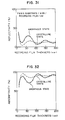
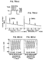
- the other is to erase a recorded bit by melting the recorded bit and crystallizing it in a solidification process (to be referred to as "liquid phase transformation"), the erasability is -15 dB as shown in Figure 2, and the number of incompletely erased parts is larger here than in the solid phase transformation.
- Sb 2 (Te-Se) 3 -GeTe described in Technical Report of Electronic Information Communication Society, Shingaku Giho, Vol. 87, No. 310, CPM87-90, 1987, page 41, erasing is carried out by solid phase transformation.
- the erasability with a laser power of 10 mW is about 30 dB as shown in Figure 3.
- the laser power is 15 mW or more, the the liquid phase transformation takes place, and the erasability becomes high. It is pointed out, however, that the high erasability is because unrecorded parts (crystal parts) are melted by irradiation with a laser power of 15 mW or more melts to become amorphous but it is not because recorded bits are erased.
- the erasing method comprises heating a spot on the film [to not less than Tm (melting point)] by increasing the laser power once in order to melt the recorded spot, and then, in the course of cooling, maintaining a temperature [of not less than Tx (crystallization temperature) and not more than Tm] by irradiating an elliptic laser spot beam of appropriate power. This method gives an erasability of -40 dB.
- the problem is that a non-erased part remains in the cases of both the solid phase transformation and the liquid phase transformation, and any high erasability cannot be achieved.
- the double beam method gives a high erasability, but requires a complicated unit therefor, which requirement is a problem.
- the optical properties (refractive index n, extinction coefficient k) of known recording films are as follows (see TABLE 1).
- the refractive indices and extinction coefficients of the known examples all fulfill the relationships of n amo ⁇ n cry and k amo ⁇ k cry, and in particular, the refractive indices in the amorphous state are characteristically smaller than those in the crystalline state.
- the term "recorded state” used in this invention refers to a completely amorphous state as well as to a state in which the crystalline phase is copresent with the amorphous phase [the amount of the amorphous phase in the recording film is 50 vol. % or more].
- the amorphous phase can be defined as a structure having random network chemical bonding of Te and the other elements, and also defined as a structure displaying no diffraction peaks in X-ray diffractometry.
- the term "erased state” in this invention refers to a completely crystalline state, as well as to a state in which the amorphous state is included in the crystalline phase [the amount of the crystalline phase in the recording film is 50 vol. % or more].
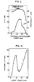
- Figure 1 is a characteristic diagram of a change of the reflectivity in recording and erasing.
- Figure 2 is a characteristic diagram of a conventional overwrite example.
- Figure 3 is a characteristic diagram of erasion in the solid phase and liquid phase.
- Figure 4 is an illustrative diagram of conventional double beam erasing and recording.
- Figure 5 is a diagram of a cooling curve and a crystallization curve.
- Figure 6 is a curve diagram of the recording and erasing principle.
- Figures 7 and 8 are explanatory diagrams of a constant power erasing principle.
- Figure 9(a) and Figure 9(b) are principle diagrams of single beam overwrite.
- Figures 10 to 14 are principle diagrams of single overwrite erasing.
- Figures 15 to 77 are explanatory diagrams of the constitutions of optical recording media and changes of reflectivity and absorptivity depending upon the thickness of the films.
- Figure 78(a) and Figure 78(b) are diagrams of recorded signal spectrum curves.
- Figure 79(a) and Figure 79(b) are characteristic diagrams of spectral at an overwriting time.
- Figure 80(a) and Figure 80(b) are characteristic diagrams of the results of overwrite repetition.
- Figure 81(a) and Figure 81(b) are characteristic diagrams of overwrite signal wave forms.
- Figure 82(a) and Figure 82(b) are spectral characteristic diagrams of In 22 Sb 37 Te 41 .
- Figure 83 is a constitutional schematic view of an optical information recording and reproducing unit.
- the values of A, R and T can be controlled on the basis of the constitution of objective media.
- the refractive index and extinction coefficient are property values inherent to the objective media and uncontrollable on the basis of the constitution of the objective media.
- the erasion has been already carried out by melting.
- High erasion performance has been achieved by a recording and erasing method, which uses a plurality of beams consisting of an elliptic laser spot beam to anneal a melted recording film and a round laser spot beam to record.
- the control system for the plurality of laser beams is complicated, and is an obstacle to practical use. It is a characteristic of this invention that high erasion performance is achieved by the melt-erasion using one single laser beam at recording and erasing times.
- the rate of cooling the recording film in the recording and erasing processes is a factor to control the formation of the amorphous phase or crystalline phase.
- a single laser beam can sufficiently control the cooling rate, it is possible to achieve the high sensitivity recording by the amorphous phase formation and the high erasability erasion by the crystalline phase formation.
- the lowest cooling rate necessary for the amorphous phase formation a so-called critical cooling rate, depends upon the crystallization rate of substances.
- the recrystallization process of the amorphous phase is a process of nucleation and growth.
- the curve which indicates the crystallization time at each degree of temperatures forms a C-shaped curve (So-called C-curve). Then, there is a temperature T n at which the crystallization time is shortest or the crystallization rate is largest.
- FIG. 5 is a typical diagram showing the temporal change of temperature (cooling curve) of a recording film when the recording film is irradiated with a laser, together with the C curve. It is to be supposed here that the crystallization time at T n is t n . In respect of the case that the maximum attainable temperature of the recording film with laser irradiation is high and the case that said maximum attainable temperature is low, if it is further to be supposed here concerning cooling curves 1 and 2 that the times during which the temperatures of the recording films reach T n (times after an input of laser irradiation) are t l and t 2 , then t 2 is larger than t n (t 2 > t n ).
- the crystallization proceeds during the cooling at a temperature of not higher than the melting point. Further, in the case of t 1 ⁇ t n , since the cooling rate is larger, the film is cooled before the crystallization is sufficiently started, whereby the amorphous phase is obtained.
- the critical cooling rate is defined to be a cooling rate at which the time during which the temperature of the recording film reaches T n is t n . In actual recording and erasing by laser irradiation, the rate of cooling the recording film is not directly controlled, but the cooling rate depends upon the stackinq structure, thermal conductivities and optical properties of components and the energy density to input.
- the conduction of heat generated at the recording film in the film surface direction is small, and the thermal conduction in the film thickness direction, in which direction heat resistance is small, is dominant.
- the higher the temperature of the recording film is the larger the temperature gradient-based outflow amount of heat per unit time is, and the cooling rate of the recording film therefore becomes large.
- T cool a characteristic temperature, i.e., a temperature higher than the melting point
- General optical recording media have a track portion on which to record information signals.
- the track in the unrecorded state is in the crystalline phase, and the signals are recorded along the track by heating local parts on the track to a temperature of not lower than T cool and cooling them rapidly to form amorphous parts.
- the characteristic of the optical recording media of this invention is that, when some recorded signals are already existent on the track, the reflectivity of the recorded parts is larger than that of the track in the unrecorded or erased state, or the absorptivity of the recorded parts is smaller than that of the track in the unrecorded or erased state.
- the attainable temperatures of these parts after the parts are melted depend upon differences among these parts in reflectivity and absorptivity.
- Figure 7 shows the absorptivity of the optical recording medium of this invention when amorphous-phase recorded parts are already existent on the track of the medium, and the temperature distribution of the track when the track is irradiated with a dc erasing laser having a constant power P 1 .
- numeral 1 indicates a heat inflow
- 2 indicates a heat outflow
- 3 indicates a recorded bit.
- the erasing power P 1 is a power to achieve an attainable temperature, in all the parts, of not lower than T and not higher than T cool .
- Figure 8 shows the absorptivity of an optical recording medium having the conventional optical properties when amorphous-phase recorded parts are existent on the track, and the temperature distribution of the track when the track is irradiated with a dc erasing laser having a constant power P 1 .
- the erasing power P 1 here is a power to achieve an attainable temperature, in all the parts, of not lower than T m and not higher than T cool .
- the existing recorded parts to be erased have a smaller absorptivity, a distribution in which the attainable temperature of the recorded parts is lower than the attainable temperature of the unrecorded areas is obtained at temperatures of not lower than the melting point.
- the absorptivity of the existing recorded areas is larger, a distribution in which the attainable temperature of the recorded areas is higher than that of the unrecorded track is obtained.
- the heat flow formed on the track due to thermal conduction is directed from the peripheral areas to the recorded area, which is to be erased. That is, the recorded area is heated by the heat flow from the unrecorded area in which the attainable temperature is higher than in the recorded area.
- This phenomenon will be denominated heat rederivation effect in the subsequent description. Since the recorded area is cooled slowly even at a temperature not higher than the melting point due to heat rederived from the area in which the attainable temperature is higher, crystalline nuclei occur in large numbers inside the existing recorded part. The nuclei grow into crystals having fine particle sizes after solidification, and the formerly recorded part is therefore crystallized, i.e., erased.
- the heat is dispersed from the recorded area to be erased to unrecorded areas, so that the cooling is not slowed down. Rather, the recorded part will cool rapidly, and the nuclei formation at a temperature around the melting point hardly takes place. Even if nuclei formation takes place, the nuclei occur in the unrecorded areas having a lower temperature, the number of nuclei occuring inside the recorded area is therefore very small, and the medium is cooled to room temperature before the crystalline growth, which occurs about the nucleus, has progressed sufficiently. It is therefore considered that the crystallized fraction of the recorded area after erasure is too small to achieve complete erasion, and incompletely erased portions remain to a large extent.
- the functional characteristic of this invention is in the optical properties of the medium, namely that the medium, per se, forms a temperature distribution on the track' which causes the heat rederivation effect.
- the single beam overwrite stands for a recording and erasing method in which existing recorded signals on the track are erased and new signals are also recorded on the same track by the use of one round laser spot beam.
- the principal difference of this method from the above-specified erasion using constant power irradiation is that a new signal is overwritten on the existing recorded area or a part thereof.
- the erasing process, per se, is essentially identical between the single beam overwrite method and the constant power erasing method.
- Figure 9(a) and Figure 9(b) show typical diagrams of laser power modulation for overwriting.
- a constant bias power P 1 is set to a level so as to melt an unrecorded area sufficiently.
- a pulse is superimposed upon the bias power P 1 to reach a power P 2 that heats the recording film to a temperature of not lower than T cool .
- signals are overwritten by changing the pulse width tw and te.
- This invention achieves high erasability at an overwriting time.
- Numeral 5 indicates a recorded bit
- 4 indicates a crystalline phase track
- 6 indicates an overwrite-recorded bit
- 7 indicates an erased bit.
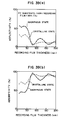
- Figure 10 shows an attainable temperature distribution on the track at an overwriting time where the existing recorded area to be erased (to be referred to as "old record” hereinbelow) and a new recording area (to be referred to as “new recording area” hereinbelow) are adjacent to each other.
- Figure 11 shows said distribution where the old record and new recording area are completely apart from each other.
- Figures 12 and 13 show said distribution where the old record and new recording area partially overlap each other.
- Figure 14 shows said distribution where the old record and new recording area completely overlap each other.
- this invention has been able to show conventionally unknown high erasing performance not only in case of a constant power irradiation and but also in case of single beam overwriting.
- this invention has like effects even when the transmissivity of optical recording media is not zero.
- optical properties of the optical recording media of this invention in which the reflectivity in the recorded state is rendered larger than that in the erased state or the absorptivity in the recorded state is rendered smaller than that in the erased state.
- the above optical property can be designed on the basis of the optical properties of a recording film, a dielectric film, a metal reflection film, etc., the thickness of each film, and the like.
- the constitutions of various media will be shown in Examples. An explanation here will be given with regard to the condition of the refractive index required to accomplish this invention.
- Figure 1 shows a change of reflectivity, at 10 5 times repetition of the static recording and erasing of an optical recording medium having a recording film (see Examples for its detailed component material) being different from conventional recording materials, having a transmissivity of nearly zero % and having a larger refractive index in the amorphous state than in the crystalline state.
- This data shows a change of reflectivity of an optical recording medium as defined in claim 1 in the actual recorded state and erased state.
- the condition specified herein with regard to the refractive index of recording films is defined by considering the limitation of optical recording media in practical use.
- the limitation of optical recording media in practical use is the limitation of the practical power of a laser source to be used for recording, reproducing and erasing.
- the recording film is melted.
- the recording film is sufficiently melted with a power in the range of practical-use laser power, i.e., not more than 15 mW on the surface of the film.
- This purpose is achieved either by using a recording film having a low melting point or by decreasing the film thickness so as to reduce the heat capacity of the recording film.
- the former procedure renders the recording film thermally unstable, and the crystallization temperature of the amorphous recorded part decreases together with the reduction of the melting point. Undesirably, therefore, there is a risk that the record maintaining life is considerably shortened.
- the latter procedure is applicable to any recording film in the range up to the thickness of the depositable film, and is therefore preferable.
- the conditions of the refractive index and extinction coefficient of recording films are defined such that the reflectivity in the recorded state is larger than the reflectivity in the erased state at the first interference in not more than 80 nm at which the recording film can be sufficiently melted even in the range of practical laser powers. Even under conditions other than those of the refractive index and extinction coefficient of the recording films defined in this invention, however, some cases satisfy the relationship each of the reflectivity and absorptivity of the disk of this invention at a second interference.
- any existing practical-use laser power is not sufficient to melt such a recording film fully.
- a practical-use larger laser power is available in the future, it will be possible to obtain the effects based on the mechanism of this invention even in the larger film thickness.
- the reflectivity, transmissivity, absorptivity, refractive index and extinction coefficient were measured as follows.
- the reflectivity R (%) and transmissivity T (%) were measured by using a spectrophotometer. Samples were prepared by forming measurement-use materials having a predetermined thickness on a substrate sheet or substrate material having supporting property such as glass, or media having various structures were used as the sample.
- the energy reflectivity was measured by a method in which, by directing light having a wavelength of 830 nm, obtained through a spectroscope, into a sample at an incident angle of 5°, reflected light was integrated by means of an integrating sphere, and directed to a light detector.
- the energy transmissivity was measured by a method in which light directed into a sample vertically from the sample surface side and transmitted by the sample was integrated by means of an integrating sphere and directed to a light detector.
- the energy absorptivity A (%) can be calculated by the following equation based on the above R and T and the law of energy conservation.
- A 100 - R - T
- the refractive index and extinction coefficient were calculated on the basis of a measured energy reflectivity and transmissivity by using a computer simulation based on matrix calculation of a multilayer system taking into account multiple reflection in the interface (see A. Bell, et al., IEEE, J. Quntum Electron, page 487, 1987).
- optical disks were prepared by a sputtering method.
- a substrate 1.2 mm in thickness quartz glass, had glass, polycarbonate (PC) resin disks and polymethylmethacryl (PMMA) resin disks were used.
- PC polycarbonate
- PMMA polymethylmethacryl
- dielectric film SiN, AlN, SiO 2 , ZrO 2 , ZnS, Ta 2 O 5 , TiN, Cr 2 O 3 , GeN, TiO 2 , SiC, etc., were used (In this Example, the dielectric films are expressed by way of chemical formula having a chemical stoichiometric composition. However, the composition changes in actual use and it is difficult to obtain an exact composition).
- chromium, Ni-20% Cr alloy and aluminum were used for a metal reflection film. Films were formed by the RF sputtering method. The sputtering conditions were that the initial degree of vacuum was 8.5 x 10 -5 Pa; an RF output of 400 W and an Ar gas partial pressure of 1 mTorr for dielectric films; an RF output of 200 W and an Ar gas partial pressure of 1 mTorr for recording films; and a DC output of 200 W and an Ar gas partial pressure of 20 mTorr for metal reflection films. Using a film of In 22 Te 37 Sb 41 (at %) as a recording film, an optical recording medium according to the invention was prepared. The optical properties of the film were examined.
- This recording film has a refractive index n of 4.952 and an extinction coefficient k of 0.857 in the amorphous state, and a refractive index n of 4.678 and an extinction coefficient k of 1.743 in the crystalline state. That is, it complies with the characteristic of this invention that the refractive index is larger in the amorphous state than in the crystalline state.
- Table 1 summarizes the refractive indices n and extinction coefficients k of the compositions discussed in the section of prior art in the present specification. In any of the compositions, the refractive index is smaller in the amorphous state than in the crystalline state, which relationship is reverse to that of this invention.
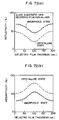
- Figure 15 shows an optical recording medium consituted of glass substrate/recording film/metal reflection film, in which the thickness of the metal reflection film 12 was constant or 100 nm, and the thickness of the recording film 9 was changed up to the maximum; of 200 nm.
- Figure 16 shows a case where gold was used for the metal reflection film 12, and the resultant medium meets the present claim 1 with regard to the change of reflectivity in the amorphous state and crystalline state.
- the thickness of the recording film in which the reflectivity difference can be substantially detected is in the range of between 30 nm and 90 nm and between 130 nm and 170 nm.
- the absorptivity difference can be substantially detected when the thickness of the recording film is between about 30 nm and 80 nm and between about 130 nm and 160 nm.
- Figure 18 and Figure 19 show cases where chromium was used for the metal reflection film 12.
- the reflectivity difference can be substantially detected when the film thickness is in the range of between about 40 nm and 80 nm and between 140 nm and 155 nm.
- Concerning the absorptivities as shown in Figure 19, the absorptivity difference can be substantially detected when the thickness of the recording film 9 is between about 40 nm and 80 nm, and about 150 nm.
- Figure 20 (a) and Figure 20(b) show cases where aluminum was used for the metal reflection film 12.
- the reflectivity difference can be substantially detected when the thickness of the recording film 9 is between about 40 nm and 90 nm and between about 130 nm and 160 nm.
- the absorptivity difference can be substantially detected when the thickness of the recording film is between about 40 nm and 80 nm, and about 154 nm.
- Figure 21(a) and Figure 21(b) show cases where Ni-20C R (wt. %) was used for the metal reflection film 12.
- the reflectivity difference can be substantially detected when the thickness of the recording film 9 is between about 50 nm and 80 nm.
- the absorptivity difference can be substantially detected in the range of between about 50 nm and 80 nm.
- Figure 22 shows a film constitution of PC substrate/recording film/metal reflection film/dielectric film, in which gold having a thickness of 100 nm was used for the metal reflection film 12, SiN having a thickness of 80 nm was used for the dielectric film 10, and the thickness of the recording film 9 was changed up to the maximum of 200 nm.
- Figure 23(a) shows changes of the reflectivities in the amorphous state and the crystalline state.
- the thickness of the recording film meeting the present claim 1 is between about 30 nm and 90 nm and between about 30 nm and 160 nm, in which ranges the reflection difference can be substantially detected.
- the absorptivity difference can be substantially detected when the thickness of the recording film is between about 30 nm and 80 nm and between 130 nm and 160 nm.
- Figure 24(a) and Figure 24(b) show a case of a film constitution of PMMA substrate/recording film/metal reflection film/dielectric film, in which chromium having a thickness of 100 nm was used for the metal reflection film 12, SiN having a thickness of 80 nm was used for the dielectric film 10, and the thickness of the recording film 9 was changed up to the maximum of 200 nm.
- Figure 24(a) shows changes of the reflectivities in the amorphous state and crystalline state.
- the thickness of the recording film 9 meeting the present claim 1 is between about 40 nm and 80 nm and between about 130 nm and 170 nm. In these thicknesses, the reflection difference can be substantially detected. Concerning the absorptivity, as shown in Figure 24(b), the absorptivity difference can be substantially detected when the thickness of the recording film 9 is between about 40 nm and 80 nm and in the vicinity of about 150 nm.
- Figure 25(a) and Figure 25(b) show a case of a film constitution of PMMA substrate/recording film/metal reflection film/dielectric film, in which aluminum having a thickness of 100 nm was used for the metal reflection film 12, SiN having a thickness of 80 nm was used for the dielectric film 10, and the thickness of the recording film 9 was changed up to the maximum of 200 nm.
- Figure 25(a) shows changes of the reflectivities in the amorphous state and crystalline state.
- the thickness of the recording film 9 meeting the present claim 1 is between about 40 nm and 90 nm and in the vicinity of about 150 nm. In these thicknesses, the reflection difference can be substantially detected. Concerning the absorptivity, as shown in Figure 25(b), the absorptivity difference can be substantially detected when the thickness of the recording film 9 is between about 40 nm and 90 nm and in the vicinity of about 150 nm.
- Figure 26 shows a film constitution of glass substrate/recording film/dielectric film/metal reflection film, in which gold having a thickness of 60 nm was used for the metal reflection film 12, AlN having a thickness of 70 nm was used for the dielectric film 10, and the thickness of the recording film 9 was changed up to the maximum of 200 nm.
- Figure 27(a) shows changes of the reflectivities in the amorphous state and crystalline state.
- the thickness of the recording film 9 meeting the present claim 1 is between about 10 nm and 65 nm and between about 105 and 140 nm. In these thickness, the reflection difference can be substantially detected. Concerning the absorptivity, as shown in Figure 27(b), the absorptivity difference can be substantially detected when the thickness of the recording film 9 is between about 10 nm and 60 nm and between about 100 nm and 140 nm.
- Figure 28 shows a film constitution of glass substrate/recording film/dielectric film/metal reflection film/dielectric film, in which gold having a thickness of 60 nm was used for the metal reflection film 12, AlN having a thickness of 70 nm was used for the dielectric film 10, and the thickness of the recording film 9 was changed up to the maximum of 200 nm.
- Figure 29(a) shows changes of the reflectivities in the amorphous state and crystalline state.
- the thickness of the recording film 9 meeting the present claim 1 is between about 10 nm and 60 nm and between about 100 and 140 nm. In these thicknesses, the reflection difference can be substantially detected. Concerning the absorptivity, as shown in Figure 29(b), the absorptivity difference can be substantially detected when the thickness of the recording film 9 is between about 10 nm and 70 nm and between about 100 nm and 140 nm.
- Figure 30 shows a film constitution of PMMA substrate/dielectric film/recording film/metal reflection film, in which aluminum having a thickness of 100 nm was used for the metal reflection film 12, AlN having a thickness of 70 nm was used for the dielectric film 10, and the thickness of the recording film 9 was changed up to the maximum of 200 nm.
- Figure 31 shows changes of the reflectivities in the amorphous state and crystalline state.
- the thickness of the recording film 9 meeting the present claim 1 is between about 20 nm and 80 nm and between about 130 and 160 nm. In these thicknesses, the reflection difference can be substantially detected. Concerning the absorptivity, as shown in Figure 32, the absorptivity difference can be substantially detected when the thickness of the recording film 9 is between about 20 nm and 80 nm and between about 130 nm and 160 nm.
- Figure 33 and Figure 34 show a case of a film constitution of PC substrate/dielectric film/ recording film/metal reflection film, in which gold having a thickness of 100 nm was used for the metal reflection film 12, AlN having a thickness of 70 nm was used for the dielectric film 10, and the thickness of the recording film 9 was changed up to the maximum of 200 nm.
- Figure 33 shows changes of the reflectivities in the amorphous state and crystalline state.
- the thickness of the recording film 9 meeting the present claim 1 is between about 10 nm and 80 nm and between about 120 nm and 160 nm. In these thicknesses, the reflection difference can be substantially detected. Concerning the absorptivity, as shown in Figure 34(b), the absorptivity difference can be substantially detected when the thickness of the recording film 9 is between about 10 nm and 80 nm and between about 120 nm and 160 nm.
- Figure 35 shows a film constitution of glass substrate/dielectric film/recording film/metal reflection film/dielectric film, in which gold having a thickness of 100 nm was used for the metal reflection film 12, AlN having a thickness of 70 nm was used for the dielectric film 10, and the thickness of the recording film 9 was changed up to the maximum of 200 nm.
- Figure 36(a) shows changes of the reflectivities in the amorphous state and crystalline state.
- the thickness of the recording film 9 meeting the present claim 1 is between about 10 nm and 80 nm and between about 120 and 160 nm. In these thicknesses, the reflection difference can be substantially detected. Concerning the absorptivity, as shown in Figure 36(b), the absorptivity difference can be substantially detected when the thickness of the recording film 9 is between about 10 nm and 80 nm and between about 120 nm and 160 nm.
- Figure 37(a) and Figure 37(b) show a case of a film constitution of PC substrate/dielectric film/ recording film/metal reflection film/dielectric film, in which aluminum having a thickness of 100 nm was used for the metal reflection film 12, AlN having a thickness of 70 nm was used for the dielectric film 10, and the thickness of the recording film 9 was changed up to the maximum of 200 nm.
- Figure 37(a) shows changes of the reflectivities in the amorphous state and crystalline state.
- the thickness of the recording film 9 meeting the present claim 1 is between about 20 nm and 80 nm and between about 130 and 160 nm. In these thicknesses, the reflection difference can be substantially detected. Concerning the absorptivity, as shown in Figure 37(b), the absorptivity difference can be substantially detected when the thickness of the recording film 9 is between about 20 nm and 85 nm and between about 130 nm and 160 nm.
- Figure 38 shows a film constitution of PC substrate/dielectric film/recording film/dielectric film/metal reflection film, in which gold having a thickness of 100 nm was used for the metal reflection film 12, AlN having a thickness of 70 nm was used for the dielectric film 10, and the thickness of the recording film 9 was changed up to the maximum of 200 nm.
- Figure 39(a) shows changes of the reflectivities in the amorphous state and crystalline state.
- the thickness of the recording film 9 meeting the present claim 1 is between about 10 nm and 70 nm and between about 90 and 150 nm. In these thicknesses, the reflection difference can be substantially detected. Concerning the absorptivity, as shown in Figure 39(b), the absorptivity difference can be substantially detected when the thickness of the recording film 9 is between about 10 nm and 70 nm and between about 90 nm and 150 nm.
- Figure 40(a) and Figure 40(b) show a case of a film constitution of glass substrate/dielectric film/ recording film/dielectric film/metal reflection film, in which aluminum having a thickness of 100 nm was used for the metal reflection film 12, AlN having a thickness of 70 nm was used for the dielectric film 10, and the thickness of the recording film 9 was changed up to the maximum of 200 nm.
- Figure 40(a) shows changes of the reflectivities in the amorphous state and crystalline state.
- the thickness of the recording film 9 meeting the present claim 1 is between about 10 nm and 70 nm and between about 90 and 150 nm. In these thicknesses, the reflection difference can be substantially detected. Concerning the absorptivity, as shown in Figure 40(b), the absorptivity difference can be substantially detected when the thickness of the recording film 9 is between about 10 nm and 70 nm and between about 70 nm and 150 nm.
- Figure 41 shows a film constitution of PC substrate/dielectric film/recording film/dielectric film/metal reflection film/dielectric film, in which gold having a thickness of 100 nm was used for the metal reflection film 12, AlN having a thickness of 70 nm was used for the dielectric film 10, and the thickness of the recording film 9 was changed up to the maximum of 200 nm.
- Figure 42(a) shows changes of the reflectivities in the amorphous state and crystalline state.
- the thickness of the recording film 9 meeting the present claim 1 is between about 10 nm and 70 nm and between about 90 and 150 nm. In these thicknesses, the reflection difference can be substantially detected. Concerning the absorptivity, as shown in Figure 42(b), the absorptivity difference can be substantially detected when the thickness of the recording film 9 is between about 10 nm and 70 nm and between about 90 nm and 150 nm.
- Figure 43(a) and Figure 43(b) show a case of a film constitution of PC substrate/dielectric film/recording film/dielectric film/metal reflection film/dielectric film, in which aluminum having a thickness of 70 nm was used for the metal reflection film 12, AlN having a thickness of 70 nm was used for the dielectric film 10, and the thickness of the recording film 9 was changed up to the maximum of 200 nm.
- Figure 43(a) shows changes of the reflectivities in the amorphous state and crystalline state.
- the thickness of the recording film 9 meeting the present claim 1 is between about 10 nm and 70 nm and between about 90 and 150 nm. In these thicknesses, the reflection difference can be substantially detected. Concerning the absorptivity, as shown in Figure 43(b), the absorptivity difference can be substantially detected when the thickness of the recording film 9 is between about 10 nm and 70 nm and between about 70 nm and 150 nm.
- Figure 44 shows a film constitution of glass substrate/recording film/metal reflection film/glass substrate, in which gold having a thickness of 100 nm was used for the metal reflection film 12 and the thickness of the recording film 9 was changed up to the maximum of 200 nm.
- Figure 45 shows changes of the reflectivities in the amorphous state and crystalline state.
- the thickness of the recording film 9 meeting the present claim 1 is between about 30 nm and 90 nm and between about 140 and 170 nm. In these thicknesses, the reflection difference can be substantially detected. Concerning the absorptivity, as shown in Figure 46, the absorptivity difference can be substantially detected when the thickness of the recording film 9 is between about 30 nm and 90 nm and between about 130 nm and 160 nm.
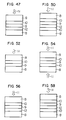
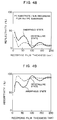
- Figure 47 shows a film constitution of PC substrate/SiN/recording film/Au/PC substrate, in which a gold having a thickness of 100 nm was used for the metal reflection film 12, SiN having a thickness of 70 nm was used for the dielectric film 10, and the thickness of the recording film 9 was changed up to the maximum of 200 nm.
- Figure 48 shows changes of the reflectivities in the amorphous state and crystalline state.
- the thickness of the recording film 9 meeting the present claim 1 is between about 10 nm and 80 nm and between about 120 and 160 nm. In these thicknesses, the reflection difference can be substantially detected. Concerning the absorptivity, as shown in Figure 49, the absorptivity difference can be substantially detected when the thickness of the recording film 9 is between about 10 nm and 80 nm and between about 120 nm and 160 nm.
- Figure 50 shows a film constitution of PC substrate/SiN/recording film/Au/SiN/PC substrate, in which gold having a thickness of 100 nm was used for the metal reflection film 12, SiN having a thickness of 70 nm was used for the dielectric film 10, and the thickness of the recording film 9 was changed up to the maximum of 200 nm.
- Figure 51(a) shows changes of the reflectivities in the amorphous state and crystalline state.
- the thickness of the recording film 9 meeting the present claim 1 is between about 10 nm and 80 nm and between about 120 and 160 nm. In these thicknesses, the reflection difference can be substantially detected. Concerning the absorptivity, as shown in Figure 51(b), the absorptivity difference can be substantially detected when the thickness of the recording film 9 is between about 10 nm and 80 nm and between about 120 nm and 160 nm.
- Figure 52 shows a film constitution of glass substrate/SiN/recording film/glass substrate, in which, SiN having a thickness of 70 nm was used for the dielectric film 10, and the thickness of the recording film 9 was changed up to the maximum of 200 nm.
- Figure 53(a) shows changes of the reflectivities in the amorphous state and crystalline state.
- the thickness of the recording film 9 meeting the present claim 1 is between about 10 nm and 60 nm and between about 100 and 140 nm. In these thicknesses, the reflection difference can be substantially detected. Concerning the absorptivity, as shown in Figure 53(b), the absorptivity difference can be substantially detected when the thickness of the recording film 9 is between about 10 nm and 200 nm.
- Figure 54 shows a film constitution of PC substrate/SiN/recording film/SiN/PC substrate, in which SiN having a thickness of 70 nm was used for the dielectric film 10, and the thickness of the recording film 9 was changed up the maximum of 200 nm.
- Figure 55(a) shows changes of the reflectivities in the amorphous state and crystalline state.
- the thickness of the recording film 9 meeting the present claim 1 is between about 10 nm and 50 nm and between about 80 and 140 nm. In these thicknesses, the reflection difference can be substantially detected. Concerning the absorptivity, as shown in Figure 55(b), the absorptivity difference can be substantially detected when the thickness of the recording film 9 is between about 10 nm and 200 nm.
- Figure 56 shows a film constitution of glass substrate/SiN/recording film/Au/glass substrate, in which gold having a thickness of 100 nm was used for the metal reflection film 12, SiN having a thickness of 70 nm was used for the dielectric film 10, and the thickness of the recording film 9 was changed up to the maximum of 200nm.
- Figure 57(a) shows changes of the reflectivities in the amorphous state and crystalline state.
- the thickness of the recording film 9 meeting the present claim 1 is between about 10 nm and 80 nm and between about 120 and 160 nm. In these thicknesses, the reflection difference can be substantially detected. Concerning the absorptivity, as shown in Figure 57(b), the absorptivity difference can be substantially detected when the thickness of the recording film 9 is between about 10 nm and 80 nm and between about 120 nm and 160 nm.
- Figure 58 shows a film constitution of PMMA substrate/SiN/recording film/Au/SiN/PMMA substrate, in which gold having a thickness of 100 nm was used for the metal reflection film 12, SiN having a thickness of 70 nm was used for the dielectric film 10, and the thickness of the recording film 9 was changed up to the maximum of 200 nm.
- Figure 59(a) shows changes of the reflectivities in the amorphous state and crystalline state.
- the thickness of the recording film 9 meeting the present claim 1 is between about 10 nm and 90 nm and between about 120 and 160 nm. In these thicknesses, the reflection difference can be substantially detected. Concerning the absorptivity, as shown in Figure 59(b), the absorptivity difference can be substantially detected when the thickness of the recording film 9 is between about 10 nm and 80 nm and between about 120 nm and 160 nm.
- Figure 60 shows a film constitution of PC substrate/AlN/recording film/AlN/Au/PC substrate, in which gold having a thickness of 100 nm was used for the metal reflection film 12, AlN having a thickness of 70 nm was used for the dielectric film 10, and the thickness of the recording film 9 was changed up to the maximum of 200 nm.
- Figure 61(a) shows changes of the reflectivities in the amorphous state and the crystalline state.
- the thickness of the recording film meeting the present claim 1 is between about 10 nm and 70 nm and between about 90 nm and 140 nm, in which ranges the reflection difference can be substantially detected.
- the absorptivity difference can be substantially detected when the thickness of the recording film 9 is between about 10 nm and 70 nm and between about 90 nm and 150 nm.
- Figure 62(a) and Figure 62(b) show a case of a film constitution of glass substrate/AlN/recording film/AlN/Ni-20 Cr/glass substrate, in which gold having a thickness of 100 nm was used for the metal reflection film 12, AlN having a thickness of 70 nm was used for the dielectric film 10, and the thickness of the recording film 9 was changed up to the maximum of 200 nm.
- Figure 62(a) shows changes of the reflectivities in the amorphous state and crystalline state.
- the thickness of the recording film 9 meeting the present claim 1 is between about 10 nm and 70 nm and between about 90 nm and 150 nm. In these thicknesses, the reflection difference can be substantially detected. Concerning the absorptivity, as shown in Figure 62(b), the absorptivity difference can be substantially detected when the thickness of the recording film 9 is between about 10 nm and 70 nm and between about 90 nm and 150 nm.
- Figure 63(a) and Figure 63(b) show a case of a film constitution of glass substrate/AlN/recording film/Al/glass substrate, in which Al having a thickness of 100 nm was used for the metal reflection film 12, AlN having a thickness of 70 nm was used for the dielectric film 10, and the thickness of the recording film 9 was changed up to the maximum of 200 nm.
- Figure 63(a) shows changes of the reflectivities in the amorphous state and crystalline state.
- the thickness of the recording film 9 meeting the present claim 1 is between about 10 nm and 70 nm and between about 90 nm and 140 nm. In these thicknesses, the reflection difference can be substantially detected. Concerning the absorptivity, as shown in Figure 63(b), the absorptivity difference can be substantially detected when the thickness of the recording film 9 is between about 10 nm and 70 nm and between about 90 nm and 150 nm.
- Figure 64 shows a film constitution of PC substrate/AlN/recording film/AlN/Au/AlN/PC substrate, in which Au having a thickness of 100 nm was used for the metal reflection film 12, AlN having a thickness of 70 nm was used for the dielectric film 10, and the thickness nf the recording film 9 was changed up to the maximum of 200 nm.
- Figure 65(a) shows changes of the reflectivities in the amorphous state and crystalline state.
- the thickness of the recording film 9 meeting the present claim 1 is between about 10 nm and 60 nm and between about 90 nm and 140 nm. In these thicknesses, the reflection difference can be substantially detected. Concerning the absorptivity, as shown in Figure 65(b), the absorptivity difference can be substantially detected when the thickness of the recording film 9 is between about 10 nm and 70 nm and between about 100 nm and 140 nm.
- Figure 66(a) and Figure 66(b) show a case of a film constitution of glass substrate/AlN/recording film/AlN/Cr/AlN/glass substrate, in which Cr having a thickness of 100 nm was used for the metal reflection film 12, AlN having a thickness of 70 nm was used for the dielectric film 10, and the thickness of the recording film 9 was changed up to the maximum of 200 nm.
- Figure 66(a) shows changes of the reflectivities in the amorphous state and crystalline state.
- the thickness of the recording film 9 meeting the present claim 1 is between about 10 nm and 70 nm and between about 90 nm and 150 nm. In these thicknesses, the reflection difference can be substantially detected. Concerning the absorptivity, as shown in Figure 66(b), the absorptivity difference can be substantially detected when the thickness of the recording film 9 is between about 10 nm and 70 nm and between about 90 nm and 140 nm.
- Figure 67(a) and Figure 67(b) show a case of a film constitution of glass substrate/AlN/recording film/AlN/Al/AlN/glass substrate, in which Al having a thickness of 100 nm was used for the metal reflection film 12, AlN having a thickness of 70 nm was used for the dielectric film 10, and the thickness of the recording film 9 was changed up to the maximum of 200 nm.
- Figure 67(a) shows changes of the reflectives in the amorphous state and crystalline state.
- the thickness of the recording film 9 meeting the present claim 1 is between about 10 nm and 70 nm and between about 100 nm and 140 nm. In these thicknesses, the reflection difference can be substantially detected. Concerning the absorptivity, as shown in Figure 67(b), the absorptivity difference can be substantially detected when the thickness of the recording film 9 is between about 10 nm and 70 nm and between about 100 nm and 140 nm.
- Figure 68(a) and Figure 68(b) show a case of a film constitution of PC substrate/AlN/recording film/AlN/Ni-20 Cr/AlN/PC substrate, in which Ni-20 Cr having a thickness of 100 nm was used for the metal reflection film 12, AlN having a thickness of 70 nm was used for the dielectric film 10, and the thickness of the recording film 9 was changed up to the maximum of 200 nm.
- Figure 68(a) shows changes of the reflectivities in the amorphous state and crystalline state.
- the thickness of the recording film 9 meeting the present claim 1 is between about 10 nm and 60 nm and between about 100 nm and 140 nm. In these thicknesses, the reflection difference can be substantially detected. Concerning the absorptivity, as shown in Figure 68(b), the absorptivity difference can be substantially detected when the thickness of the recording film 9 is between about 10 nm and 70 nm and between about 100 nm and 140 nm.
- Figure 69 shows a film constitution of glass substrate/recording film/Au/glass substrate, in which gold having a thickness of 10 nm was used for the metal reflection film 12 and the thickness of the recording film 9 was changed up to the maximum of 200 nm.
- Figure 70(a) shows changes of the reflectivities in the amorphous state and crystalline state.
- the thickness of the recording film 9 meeting the present claim 1 is between about 20 nm and 70 nm and between about 120 nm and 150 nm. In these thicknesses, the reflection difference can be substantially detected. Concerning the absorptivity, as shown in Figure 70(b), the absorptivity difference can be substantially detected when the thickness of the recording film 9 is between about 10 nm and 160 nm.
- Figure 71(a) and Figure 71(b) show the reflectivity and absorptivity of a film using In 22 Sb 37 Te 41 (at %) of this invention and having a film constitution of glass substrate/dielectric film/recording film/dielectric film/metal reflection film/dielectric film when the dielectric film 10 positioned as a fourth layer from the glass substrate was changed up to 200 nm.
- Gold having a thickness of 100 nm was used for the metal reflection film 12, and SiO 2 having a thickness of 70 nm was used as the other dielectric films 10.
- Figure 71(a) shows changes of the reflectivities in the amorphous state and crystalline state, and the reflection difference can be substantially detected in all the range of the thickness of the dielectric film 10 meeting the present claim 1. Further, concerning the absorptivity, as shown in Figure 71(b), the absorptivity difference can be substantially detected in all the range of the thickness of the dielectric film 10 as well.
- Figure 72(a) and Figure 72(b) show the reflectivity and absorptivity of a film using In 22 Sb 37 Te 41 (at %) of this invention and having a film constitution of glass substrate/dielectric film/recording film/dielectric film/metal reflection film/dielectric film when the dielectric film 10 positioned as a second layer from the glass substrate was changed up to 200 nm.
- Gold having a thickness of 100 nm was used for the metal reflection film 12
- AlN having a thickness of 70 nm was used as the other dielectric films 10.
- Figure 72(a) shows changes of the reflectivities in the amorphous state and crystalline state, and the reflection difference can be substantially detected in all the range of the thickness of the dielectric film 10 meeting the present claim 1. Further, concerning the absorptivity, as shown in Figure 72(b), the absorptivity difference can be substantially detected in all the range of the thickness of the dielectric film 10 as well.
- Figure 73(a) and Figure 73(b) show a case where Se 52 Ge 27 Sn 21 (at %) was used as a recording material meeting the present claims 1, 7, 13 and 19.
- the film constitution was PMMA substrate/dielectric film/recording film/dielectric film/metal reflection film/dielectric film, Gold having a thickness of 100 nm was used for the metal reflection film 12, ZrO 2 having a thickness of 70 nm was used as the dielectric films 10, and the thickness of the recording film 9 was changed up to the maximum of 200 nm.
- Figure 73(a) shows changes of the reflectivities in the amorphous state and crystalline state, and the reflection difference can be substantially detected when the thickness of the recording film 9 meeting the present claim 1 is between about 10 nm and 80 nm and between about 100 nm and 180 nm. Further, concerning the absorptivity, as shown in Figure 73(b), the absorptivity difference can be substantially detected when the thickness of the recording film 9 is between about 10 nm and 80 nm and between about 100 nm and 180 nm.
- Figure 74(a) and Figure 74(b) show a case where Sb 56 Se 40 Zn 4 (at %) was used as a recording material meeting the present claims 1, 7, 13 and 19.
- the film constitution was PC substrate/dielectric film/recording film/dielectric film/metal reflection film/dielectric film, Gold having a thickness of 100 nm was used for the metal reflection film 12, ZrO 2 having a thickness of 70 nm was used as the dielectric films 10, and the thickness of the recording film 9 was changed up to the maximum of 200 nm.
- Figure 74(a) shows changes of the reflectivities in the amorphous state and crystalline state, and the reflection difference can be substantially detected when the thickness of the recording film 9 meeting the present claim 1 is between about 10 nm and 80 nm and between about 110 nm and 120 nm. Further, concerning the absorptivity, as shown in Figure 74(b), the absorptivity difference can be substantially detected when the thickness of the recording film 9 is between about 10 nm and 80 nm and between about 100 nm and 180 nm.
- Figure 75(a) and Figure 75(b) show a case where Sb 34 Se 58 Sn 8 (at %) was used as a recording material meeting the present claims 1, 7, 13 and 19.
- the film constitution was PC substrate/dielectric film/recording film/dielectric film/metal reflection film/dielectric film, Gold having a thickness of 100 nm was used for the metal reflection film 12, AlN having a thickness of 70 nm was used as the dielectric films 10, and the thickness of the recording film 9 was changed up to the maximum of 200 nm.
- Figure 75(a) shows changes of the reflectivities in the amorphous state and crystalline state, and the reflection difference can be substantially detected in all the range of the thickness of the recording film 9 meeting the present claim 1. Further, concerning the absorptivity, as shown in Figure 75(b), the absorptivity difference can be substantially detected in all the range of the thickness of the recording film 9 as well.
- Figure 76(a) and Figure 76(b) show a case where Sb 64 Se 29 Zn 27 (at %) was used as a recording material meeting the present claims 1, 7, 13 and 19.
- the film constitution was PMMA substrate/dielectric film/recording film/dielectric film/metal reflection film/dielectric film, gold having a thickness of 100 nm was used for the metal reflection film 12, SiN having a thickness of 70 nm was used as the dielectric films 10, and the thickness of the recording film 9 was changed up to the maximum of 200 nm.
- Figure 76(a) shows changes of the reflectivities in the amorphous state and crystalline state, and the reflection difference can be substantially detected in all the range of the thickness of the recording film 9 meeting the present claim 1. Further, concerning the absorptivity, as shown in Figure 76(b), the absorptivity difference can be substantially detected in all the range of the thickness of the recording film 9 as well.
- Figure 77(a) and Figure 77(b) show a case where Te 64 Sb 6 Sn 30 (at %) was used as a recording material meeting the present claims 1, 7, 13 and 19.
- the film constitution was PMMA substrate/dielectric film/recording film/dielectric film/metal reflection film/dielectric film, Gold having a thickness of 100 nm was used for the metal reflection film 12, AlN having a thickness of 70 nm was used as the dielectric films 10, and the thickness of the recording film 9 was changed up to the maximum of 200 nm.
- Figure 77(a) shows changes of the reflectivities in the amorphous state and crystalline state, and the reflection difference can be substantially detected in all the range of the thickness of the recording film 9 meeting the present claim 1. Further, concerning the absorptivity, as shown in Figure 77(b), the absorptivity difference can be substantially detected in all the range of the thickness of the recording film 9 as well.
- Figure 78(a) and Figure 78(b) show an embodiment of recording and erasing with regard to rewritable disks using optical recording media recited in the present claims 7, 13, 19 and 35.
- the disks were prepared according to a high frequency sputtering method which comprises depositing 70 nm to 80 nm thick AlN for an optical interference film on 5.25 inch glass substrates having a laser guide groove for laser beam tracking of the continuous-servo tracking technique, 30 nm to 50 nm thick In 22 Sb 37 Te 41 for a recording film thereon, 70 to 80 nm thick AlN thereon, 100 nm thick Au for an optical reflection film thereon, and 100 nm thick AlN for a protective film thereon.
- Figure 79(a) and Figure 79(b) show an embodiment of the single beam overwrite with regard to rewritable optical disks using the optical recording medium of this invention.
- the disk constitution was the same as that of the above embodiment.
- Figure 79(a) shows a power modulation mode of a round laser spot beam (spot diameter: about 1.5 ⁇ m) used for the overwriting.
- a recording power P 1 which can heat a recording film to a temperature of not less than T cool
- a bias power P 2 which can heat the recording film to a temperature of between not less than the melting point and not more than T cool .
- the disks were turned at 1,800 to 2,400 rounds/minute, and continuously irradiated with a 15 mW constant power beam to reduce the disk reflectivity from about 50% to about 20%, whereby a recording track portion was formed. Then, sine wave signals having a modulated frequency of 2 MHz were recorded by irradiation of a laser having the above power, and thereafter, 3 MHz sine wave signals were recorded by overwriting the 2 MHz signals.
- Figure 81(a) and Figure 81(b) show 2 MHz sine wave signals on an oscilloscope screen. Any deformation of waveforms and change of frequency due to incomplete erasion wave recognized in any of the signals, and the signals were completely erased in both the cases. It has been demonstrated that the optical recording media of this invention make it possible to perform a single beam overwrite free from incomplete erasion even with a practical-use laser power of 15 mW or less. And when resin substrates such as PMMA, PC, etc., were used as the substrate, it was also possible to obtain results identical with those of the above embodiment. Further, in the case of using disks according to another tracking system, sampled-servo tracking technique, the optical recording media of this invention were also able to give the same results as those of the above embodiment.
- the recording films described in Table 2 constitute the optical recording media which have a larger reflectivity, n, in the amorphous state than in the crystalline state and actually satisfy the present claim 1, and the changes therein are different from those in the conventional materials described in Table 1.
- the recording films comprise compounds of elements such as antimony, zinc, tin, germanium, etc., with selenium, tellurium, etc. Elements such as indium, lead, silver, copper, gold, etc., are also effective to control the refractive index of the recording film.
- Table 3 shows the recordability and erasability of optical disks having the recording films described in Table 2.
- the disks were prepared according to the high frequency sputtering method which comprises depositing 70 nm to 80 nm thick AlN, for an optical interference film, on a 5.25 inch glass substrate having a laser guide groove for laser beam tracking of continuous servo technique, 330 nm to 50 nm thick recording material selected from the recording films described in Table 2 thereon, 100 nm thick Au for an optical reflection film thereon and 100 nm thick AlN for a protective film thereon.
- the recording power and erasing power were 15 mW or less.
- All the resultant optical disks gave a C/N of about 50 dB and were of high sensitivity, and further, these optical disks were able to give a high erasability of -35 dB or more in both the constant power and overwrite erasing methods.
- the recording media gave high-sensitivity recording and high erasability, and there is no special limitation to be imposed on the wavelength for use.
- optical recording media satisfying the reflectivity and absorptivity in the as-deposited state and the reflectivity and absorptivity in the recorded and erased states described in present claim 2, a track having a lower reflectivity (often equivalent to the reflectivity in the erased state) than that in the as-deposited state is first formed, and signals are recorded on the track.
- the other portion (outside the track and corresponding to a groove of a disk for the continuous servo technique) is that which has a higher reflectivity (or a lower absorptivity) and remains in the as-deposited state.
- the cross-talk increase in the minimizing of the intertrack distance determines the recording density on the optical recording media.
- the outside-the-track portion having a smaller reflectivity and being in the as-deposited state is positioned in contact with the track portion.
- the outside-the-track portion is less influenced thermally by a laser power used for the recording and erasing on the track portion, since its attainable temperature is low.
- the cross-talk to an adjacent track is reduced especially by this thermal block.
- the cross-talk is as small as -40 dB or less, which value is very small as compared with conventional ones.
- the relationship in the reflectivities or absorptivities is reverse to that in this invention, and the outside-the-track portion is therefore likely to be thermally influenced.
- the above effect can be produced only by the optical recording media of this invention, and it is made possible to perform the recording in an unconventionally higher density.
- Figure 83 is a block diagram of a unit showing a process for optical information recording and reproducing as one embodiment of this invention.
- the unit comprises an optical pickup 13, an optical pickup position control circuit 14, a received signal processing circuit 15, a laser diode actuating circuit 16, a disk-turning motor 17, a turn table 18, an optical disk 19 with a tracking guide, a melting point discrimination processing portion 20 for the recording film of an optical disk, a system control circuit 21, and a set of external input-output terminals 22.
- the optical disk has a constitution in which a 70 nm thick AlN film is sputtering-formed on a glass substrate, a 50 nm thin film of In-Sb-Te type as a recording film is formed thereon by sputtering, a 70 nm thick AlN film is again formed thereon by sputtering, a 100 nm thick Au film is further formed thereon by sputtering, a 100 nm thick AlN film as a protective film is formed thereon, and a 10 ⁇ m thick UV-hardening resin film as a protective film is finally spin-coated thereon.
- the above optical disk 19 is placed on the turn table 18, and the motor 17 turns the turn table 18 to turn the optical disk 19.
- the turning is switched on or off through the external input-output terminals 21 via the system control circuit 21.
- the optical disk 19 is irradiated with a laser beam 23 from the optical pickup 13.
- a reflected beam portion of the laser beam 23 returns to the optical pickup 13 to extract an optical pickup height signal and deflection signal on the track through the received signal processing circuit 15.
- the optical pickup position control circuit 14 controls the focusing and tracking of the optical pickup 13 on the disk 19.
- the focusing and tracking are switched on or off through the external input-output terminals 22 via the system control circuit 21.
- the optical pickup 13 has a constitution such that the system control circuit 21 sets a laser irradiation power as required in keeping with the passage of time through the laser diode actuating circuit 16 whereby the overwrite is possible by using one beam.
- a laser irradiation power necessary to heat the optical disk 19 to a temperature of its melting point or more is written in a control track provided in the inner or outer circumference of the optical disk 19, and at the time of overwriting, the melting point discrimination processing portion 20 sets the recording point irradiation power and erasing point irradiation power at a power necessary to heat to the melting point or more.
- the melting point discrimination processing portion 20 can read the above written data to overwrite at a temperature of the melting point or more, or a power P M for heating to the melting point may be determined on the basis of reflectivity changes obtained while effecting a laser irradiation by using a dummy track as follows.
- This invention provides recording media having high erasing performance and high density recordability which conventional media do not have and information recording and reproducing units.
Landscapes
- Chemical & Material Sciences (AREA)
- Inorganic Chemistry (AREA)
- Thermal Transfer Or Thermal Recording In General (AREA)
- Optical Record Carriers And Manufacture Thereof (AREA)
- Optical Recording Or Reproduction (AREA)
Claims (10)
- Optisches Aufzeichnungsmedium, mit einem Substrat (8), einem dielektrischen Film (10) und einem Aufzeichnungsfilm (9), der eine kristalline Phase und eine amorphe Phase besitzt, wobei die Mediuminformationen durch Ändern der Phase des Aufzeichnungsfilms (9) aufgezeichnet und gelöscht werden,
dadurch gekennzeichnet, daß
auf einer Seite des Aufzeichnungsfilms (9) ein Metallreflexionsfilm (12) vorgesehen ist und daß das Reflexionsvermögen des Aufzeichnungsmediums bei einer Wellenlänge im Bereich von 600 bis 860 nm in einer Fläche, in der sich der Aufzeichnungsfilm (9) in der amorphen Phase befindet, höher als in ein einer Fläche ist, in der der er in der kristallinen Phase ist. - Optisches Aufzeichnungsmedium nach Anspruch 1, dadurch gekennzeichnet, daß das Reflexionsvermögen des Aufzeichnungsmediums in einer Fläche, in der der Aufzeichnungsfilm (9) in einem Zustand wie abgelagert ist, höher als in einer Fläche ist, in der er im amorphen Zustand ist.
- Optisches Aufzeichnungsmedium nach Anspruch 2, gekennzeichnet durch einen Spurabschnitt für die Aufzeichnung von Informationen, der durch eine partielle Laserbestrahlung des Aufzeichnungsfilms (9) in dem Zustand wie abgelagert gebildet wird, und durch einen Abschnitt außerhalb der Spur, der im Zustand wie abgelagert bleibt und ein höheres Reflexionsvermögen als der Spurabschnitt besitzt.
- Optisches Aufzeichnungsmedium nach einem der Ansprüche 1 bis 3, dadurch gekennzeichnet, daß der Aufzeichnungsfilm eine der folgenden Zusammensetzungen besitzt:- InxSbyTez, 15 < x < 35, 25 < y < 50, 25 < z < 50 (in Atom-%)- SbxSeyZn(100-x-y), 44≤ x≤ 56, 29 ≤ y ≤ 40 (in Atom-%)- Sb34Se58Sn8 (in Atom-%)- Se52Ge27Sn21 (in Atom-%)- Te64Sb6Sn30 (in Atom-%)- oder Se66Sb24Ge10 (in Atom-%).
- Optisches Aufzeichnungsmedium nach Anspruch 4, dadurch gekennzeichnet, daß der dielektrische Film (10) aus einer der Verbindungen SiN, AlN, SiO2, ZrO2, ZnS, Ta2O5, TiN, Cr2O3, GeN, TiO2 und SiC in einer im wesentlichen stöchiometrischen Zusammensetzung besteht.
- Optisches Aufzeichnungsmedium nach Anspruch 4, dadurch gekennzeichnet, daß der Metallreflexionsfilm (12) aus einer Ni-(20 %)-Cr-Legierung, Au oder Al besteht.
- Optisches Aufzeichnungsmedium nach einem der Ansprüche 1 bis 6, das eine der folgenden Strukturen besitzt, wobei das lichtdurchlässige Substrat, die lichtdurchlässige Folie oder das lichtdurchlässige Band mit S abgekürzt ist:S/Aufzeichnungsfilm/Metallreflexionsfilm/dielektrischer Film,S/Aufzeichnungsfilm/dielektrischer Film/Metallreflexionsfilm,S/Aufzeichnungsfilm/dielektrischer Film/Metallreflexionsfilm/dielektrischer Film,S/dielektrischer Film/Aufzeichnungsfilm/Metallreflexionsfilm,S/dielektrischer Film/Aufzeichnungsfilm/Metallreflexionsfilm/dielektrischer Film,S/dielektrischer Film/Aufzeichnungsfilm/dielektrischer Film/Metallreflexionsfilm,S/dielektrischer Film/Aufzeichnungsfilm/dielektrischer Film/Metallreflexionsfilm/dielektrischer Film,S/Aufzeichnungsfilm/dielektrischer Film/Metallreflexionsfilm/S,S/Aufzeichnungsfilm/dielektrischer Film/Metallreflexionsfilm/dielektrischer Film/S,S/dielektrischer Film/Aufzeichnungsfilm/Metallreflexionsfilm/S,S/dielektrischer Film/Aufzeichnungsfilm/Metallreflexionsfilm/dielektrischer Film/S,S/dielektrischer Film/Aufzeichnungsfilm/dielektrischer Film/Metallreflexionsfilm/S undS/dielektrischer Film/Aufzeichnungsfilm/dielektrischer Film/Metallreflexionsfilm/dielektrischer Film/S.
- Optisches Aufzeichnungsmedium nach einem der Ansprüche 1-7, dadurch gekennzeichnet, daß das Material des Aufzeichnungsfilms (9) so gewählt ist, daß es im amorphen Zustand einen höheren Brechungsindex als im kristallinen Zustand besitzt und im amorphen Zustand einen niedrigeren Extinktionskoeffizienten als im kristallinen Zustand besitzt.
- Optisches Aufzeichnungs-/Wiedergabesystem, mit einem Laser zum Aufzeichnen und Löschen von Informationen auf einem Aufzeichnungsmedium mit einer Laserwellenlänge in der Umgebung von 800 oder 830 nm, dadurch gekennzeichnet, daß Aufzeichnungsmedium ein Aufzeichnungsmedium nach einem der Ansprüche 1-8 ist.
- Prozeß zum Aufzeichnen und Löschen von Informationen in einem optischen Aufzeichnungsmedium nach einem der Ansprüche 1-8, wobei das Löschen durch Bestrahlen des das optische Aufzeichnungsmedium bildenden Aufzeichnungsfilms (9) mit einem Laserstrahl ausgeführt wird, um seine Temperatur auf einen Wert über seinem Schmelzpunkt, jedoch unterhalb einer minimalen Temperatur, die für die Bildung der amorphen Phase erforderlich ist, zu erhöhen und den Aufzeichnungsfilm (9) zu schmelzen, und das Aufzeichnen durch Bestrahlen des Aufzeichnungsfilms (9) ausgeführt wird, um seine Temperatur auf einen Wert über der minimalen Temperatur zu erhöhen und den Aufzeichnungsfilm (9) zu löschen.
Priority Applications (1)
| Application Number | Priority Date | Filing Date | Title |
|---|---|---|---|
| EP97104514A EP0784316B1 (de) | 1988-06-24 | 1989-06-19 | Optische Aufzeichnungsträger und Informationseinheiten zur Aufzeichnung und Wiedergabe |
Applications Claiming Priority (2)
| Application Number | Priority Date | Filing Date | Title |
|---|---|---|---|
| JP154743/88 | 1988-06-24 | ||
| JP63154743A JP2512087B2 (ja) | 1988-06-24 | 1988-06-24 | 光記録媒体および光記録方法 |
Related Child Applications (2)
| Application Number | Title | Priority Date | Filing Date |
|---|---|---|---|
| EP97104514A Division EP0784316B1 (de) | 1988-06-24 | 1989-06-19 | Optische Aufzeichnungsträger und Informationseinheiten zur Aufzeichnung und Wiedergabe |
| EP97104514.1 Division-Into | 1997-03-17 |
Publications (3)
| Publication Number | Publication Date |
|---|---|
| EP0347801A2 EP0347801A2 (de) | 1989-12-27 |
| EP0347801A3 EP0347801A3 (de) | 1991-12-11 |
| EP0347801B1 true EP0347801B1 (de) | 1997-09-24 |
Family
ID=15590945
Family Applications (2)
| Application Number | Title | Priority Date | Filing Date |
|---|---|---|---|
| EP97104514A Expired - Lifetime EP0784316B1 (de) | 1988-06-24 | 1989-06-19 | Optische Aufzeichnungsträger und Informationseinheiten zur Aufzeichnung und Wiedergabe |
| EP89111107A Expired - Lifetime EP0347801B1 (de) | 1988-06-24 | 1989-06-19 | Optisches Aufzeichnungsmedium und Systeme zur Informationsaufzeichnung und Wiedergabe |
Family Applications Before (1)
| Application Number | Title | Priority Date | Filing Date |
|---|---|---|---|
| EP97104514A Expired - Lifetime EP0784316B1 (de) | 1988-06-24 | 1989-06-19 | Optische Aufzeichnungsträger und Informationseinheiten zur Aufzeichnung und Wiedergabe |
Country Status (7)
| Country | Link |
|---|---|
| US (2) | US5484686A (de) |
| EP (2) | EP0784316B1 (de) |
| JP (1) | JP2512087B2 (de) |
| KR (1) | KR0144001B1 (de) |
| CN (1) | CN1018303B (de) |
| CA (1) | CA1332467C (de) |
| DE (2) | DE68928337T2 (de) |
Families Citing this family (29)
| Publication number | Priority date | Publication date | Assignee | Title |
|---|---|---|---|---|
| US5291470A (en) * | 1988-03-28 | 1994-03-01 | Matsushita Electric Industrial Co., Ltd. | Optical information recording method |
| JP2538647B2 (ja) * | 1988-07-22 | 1996-09-25 | 富士通株式会社 | 光ディスク媒体 |
| JPH02249136A (ja) * | 1989-03-23 | 1990-10-04 | Asahi Chem Ind Co Ltd | 光学的記録再生装置 |
| DE4019301A1 (de) * | 1990-06-16 | 1991-12-19 | Basf Ag | Reversibler optischer aufzeichnungstraeger vom phasenwechsel-typ |
| JP2750018B2 (ja) * | 1990-07-13 | 1998-05-13 | インターナショナル・ビジネス・マシーンズ・コーポレイション | 光学記録媒体及び光学データ記録ディスクドライブシステム |
| US5242784A (en) * | 1990-07-13 | 1993-09-07 | International Business Machines Corporation | System and method for optical phase change recording |
| JP2556183B2 (ja) * | 1990-09-11 | 1996-11-20 | 富士ゼロックス株式会社 | 光学的記録方法とこの方法を用いる光記録媒体 |
| JP2987223B2 (ja) * | 1991-02-20 | 1999-12-06 | ティーディーケイ株式会社 | 光記録媒体 |
| JP3076412B2 (ja) * | 1991-07-24 | 2000-08-14 | 松下電器産業株式会社 | 光学的情報記録媒体および光学的情報記録再生方法 |
| US5424106A (en) * | 1992-04-17 | 1995-06-13 | Matsushita Electric Industrial Co., Ltd. | Optical information recording medium and method of designing its structure |
| JPH0778354A (ja) * | 1993-09-07 | 1995-03-20 | Toshiba Corp | 情報記録媒体およびそれを用いた記録方法 |
| JP2806274B2 (ja) * | 1994-10-19 | 1998-09-30 | 日本電気株式会社 | 光学情報記録媒体 |
| CN1054227C (zh) * | 1994-10-31 | 2000-07-05 | 北京航空航天大学 | 记录媒体及其记录和擦除方法 |
| US6821707B2 (en) | 1996-03-11 | 2004-11-23 | Matsushita Electric Industrial Co., Ltd. | Optical information recording medium, producing method thereof and method of recording/erasing/reproducing information |
| US5889756A (en) * | 1996-07-25 | 1999-03-30 | Kabushiki Kaisha Toshiba | Phase change optical recording medium |
| US6503690B1 (en) | 1997-08-12 | 2003-01-07 | Matsushita Electric Industrial Co., Ltd. | Optical information recording medium, method for producing the same, and method for recording and reproducing optical information |
| JPH11134720A (ja) * | 1997-08-28 | 1999-05-21 | Matsushita Electric Ind Co Ltd | 光学的情報記録媒体及びその記録再生方法 |
| US6343062B1 (en) | 1997-09-26 | 2002-01-29 | Matsushita Electric Industrial Co., Ltd | Optical disk device and optical disk for recording and reproducing high-density signals |
| TW448443B (en) | 1998-08-05 | 2001-08-01 | Matsushita Electric Industrial Co Ltd | Optical information storage media and production method as well as the storage reproducing method and device |
| BR0107435A (pt) * | 2000-11-06 | 2002-10-08 | Matsushita Electric Industrial Co Ltd | Meio de gravação ótico, processo de fabricação de meio de gravação ótico, aparelho para fabricação de meio de gravação ótico, programa, e meio |
| US6846611B2 (en) * | 2001-02-28 | 2005-01-25 | Ricoh Company, Ltd. | Phase-change optical recording medium |
| JP2003162821A (ja) * | 2001-11-27 | 2003-06-06 | Tdk Corp | 光記録媒体および光記録方法 |
| US6798711B2 (en) * | 2002-03-19 | 2004-09-28 | Micron Technology, Inc. | Memory with address management |
| JP2005174528A (ja) | 2003-11-18 | 2005-06-30 | Hitachi Maxell Ltd | 光ディスク及びその製造方法並びに記録再生装置 |
| USRE47382E1 (en) * | 2005-07-18 | 2019-05-07 | Xenogenic Development Limited Liability Company | Back-to-back metal/semiconductor/metal (MSM) Schottky diode |
| JP4576316B2 (ja) | 2005-10-20 | 2010-11-04 | 株式会社日立製作所 | サーボ制御信号生成装置、光ディスク装置及びサーボ制御信号生成方法 |
| KR100856326B1 (ko) * | 2006-07-19 | 2008-09-03 | 삼성전기주식회사 | 레이저 리프트 오프를 이용한 유전체 박막을 갖는 박막 커패시터 내장된 인쇄회로기판 제조방법, 및 이로부터 제조된 박막 커패시터 내장된 인쇄회로기판 |
| TWI402829B (zh) * | 2010-10-29 | 2013-07-21 | Nat Univ Tsing Hua | 多階記錄方法及其系統 |
| KR102383501B1 (ko) * | 2015-01-08 | 2022-04-07 | 삼성전자주식회사 | 다층 박막, 그 제조 방법 및 이를 포함하는 전자 제품 |
Family Cites Families (28)
| Publication number | Priority date | Publication date | Assignee | Title |
|---|---|---|---|---|
| US3716844A (en) * | 1970-07-29 | 1973-02-13 | Ibm | Image recording on tetrahedrally coordinated amorphous films |
| US3971874A (en) * | 1973-08-29 | 1976-07-27 | Matsushita Electric Industrial Co., Ltd. | Optical information storage material and method of making it |
| US4330833A (en) * | 1978-05-26 | 1982-05-18 | Vicom Systems, Inc. | Method and apparatus for improved digital image processing |
| US4264986A (en) * | 1979-03-12 | 1981-04-28 | Willis Craig I | Information-recording process & apparatus |
| DE3118058A1 (de) * | 1980-05-14 | 1982-03-11 | RCA Corp., 10020 New York, N.Y. | Aufzeichnungstraeger und verfahren zum schreiben einer informationsspur sowie zum loeschen einer in dem traeger gespeicherten information |
| US4460636A (en) * | 1981-03-27 | 1984-07-17 | Sony Corporation | Optical information record member |
| JPS59185048A (ja) * | 1983-04-01 | 1984-10-20 | Matsushita Electric Ind Co Ltd | 光学情報記録部材及び記録方法 |
| US4587209A (en) * | 1984-03-28 | 1986-05-06 | Matsushita Electric Industrial Co., Ltd. | Optical information recording member comprising Au, TeO2 and Te |
| JPS60231928A (ja) * | 1984-04-27 | 1985-11-18 | Matsushita Electric Ind Co Ltd | 光学情報記録消去方法 |
| KR890004230B1 (ko) * | 1984-08-24 | 1989-10-27 | 가부시끼가이샤 도오시바 | 광(光) 디스크 메모리 |
| JPS6196541A (ja) * | 1984-10-18 | 1986-05-15 | Nec Corp | 光磁気記録媒体 |
| JPH0619856B2 (ja) * | 1984-11-09 | 1994-03-16 | 株式会社日立製作所 | 情報記録媒体 |
| US4651172A (en) * | 1984-11-29 | 1987-03-17 | Hitachi, Ltd. | Information recording medium |
| JPS61156545A (ja) * | 1984-12-28 | 1986-07-16 | Tdk Corp | 情報記録媒体および記録方法 |
| DE3671122D1 (de) * | 1985-02-22 | 1990-06-13 | Asahi Chemical Ind | Informationsaufzeichnungsmedium. |
| JPS61210538A (ja) * | 1985-03-14 | 1986-09-18 | Victor Co Of Japan Ltd | 記録媒体用インジウム−ニオビウム合金 |
| JPH0734267B2 (ja) * | 1985-05-24 | 1995-04-12 | 松下電器産業株式会社 | 可逆的光学情報記録媒体および記録再生方法 |
| US4710899A (en) * | 1985-06-10 | 1987-12-01 | Energy Conversion Devices, Inc. | Data storage medium incorporating a transition metal for increased switching speed |
| US4787077A (en) * | 1985-08-15 | 1988-11-22 | International Business Machines Corporation | Process for optically storing information using materials having a single phase in both the crystalline state and the amorphous state |
| JPS6286553A (ja) * | 1985-10-11 | 1987-04-21 | Matsushita Electric Ind Co Ltd | 光学情報記録部材 |
| US4818666A (en) * | 1986-03-28 | 1989-04-04 | U.S. Philips Corporation | Erasable optical recording element and method of optically recording and erasing information |
| DE3751891T2 (de) * | 1986-05-02 | 1997-04-03 | Hitachi Ltd | Methode zur Aufzeichnung, Wiedergabe und zum Löschen von Informationen und Dünnfilm zur Aufzeichnung von Informationen |
| JPS63187430A (ja) * | 1987-01-30 | 1988-08-03 | Toshiba Corp | 情報記録媒体 |
| JPS63188836A (ja) * | 1987-01-30 | 1988-08-04 | Sanyo Electric Co Ltd | 光学記録媒体 |
| DE3705389A1 (de) * | 1987-02-20 | 1988-09-01 | Basf Ag | Substituierte crotonsaeureester und diese enthaltende fungizide |
| JPS63251290A (ja) * | 1987-04-08 | 1988-10-18 | Hitachi Ltd | 光記録媒体と記録・再生方法及びその応用 |
| JPH081707B2 (ja) * | 1987-12-04 | 1996-01-10 | 松下電器産業株式会社 | 光学的情報記録媒体 |
| JPH01165043A (ja) * | 1987-12-21 | 1989-06-29 | Fuji Electric Co Ltd | 光記録媒体 |
-
1988
- 1988-06-24 JP JP63154743A patent/JP2512087B2/ja not_active Expired - Fee Related
-
1989
- 1989-06-13 CA CA000602705A patent/CA1332467C/en not_active Expired - Fee Related
- 1989-06-19 EP EP97104514A patent/EP0784316B1/de not_active Expired - Lifetime
- 1989-06-19 DE DE68928337T patent/DE68928337T2/de not_active Expired - Fee Related
- 1989-06-19 EP EP89111107A patent/EP0347801B1/de not_active Expired - Lifetime
- 1989-06-19 DE DE68929438T patent/DE68929438T2/de not_active Expired - Fee Related
- 1989-06-23 KR KR1019890008701A patent/KR0144001B1/ko not_active Expired - Fee Related
- 1989-06-24 CN CN89106296A patent/CN1018303B/zh not_active Expired
-
1994
- 1994-03-04 US US08/205,768 patent/US5484686A/en not_active Ceased
-
1998
- 1998-01-15 US US09/008,847 patent/USRE36624E/en not_active Expired - Lifetime
Also Published As
| Publication number | Publication date |
|---|---|
| USRE36624E (en) | 2000-03-21 |
| CA1332467C (en) | 1994-10-11 |
| KR0144001B1 (ko) | 1998-07-15 |
| DE68928337D1 (de) | 1997-10-30 |
| CN1018303B (zh) | 1992-09-16 |
| JPH025238A (ja) | 1990-01-10 |
| EP0784316A2 (de) | 1997-07-16 |
| KR910001677A (ko) | 1991-01-31 |
| US5484686A (en) | 1996-01-16 |
| EP0784316A3 (de) | 1998-09-23 |
| EP0347801A3 (de) | 1991-12-11 |
| DE68929438T2 (de) | 2003-06-12 |
| DE68929438D1 (de) | 2003-01-09 |
| JP2512087B2 (ja) | 1996-07-03 |
| CN1039920A (zh) | 1990-02-21 |
| DE68928337T2 (de) | 1998-04-09 |
| EP0784316B1 (de) | 2002-11-27 |
| EP0347801A2 (de) | 1989-12-27 |
Similar Documents
| Publication | Publication Date | Title |
|---|---|---|
| EP0347801B1 (de) | Optisches Aufzeichnungsmedium und Systeme zur Informationsaufzeichnung und Wiedergabe | |
| EP0180103B1 (de) | Verfahren zur Herstellung einer optischen Datenspeicherungsvorrichtung und die dadurch hergestellte optische Datenspeicherungsvorrichtung | |
| EP0294932B1 (de) | Verfahren zum Aufzeichnen und Löschen von Daten | |
| US5688574A (en) | Optical recording medium | |
| JP3566743B2 (ja) | 光記録媒体 | |
| EP0373955B1 (de) | Optischer Aufzeichnungsträger | |
| US6333913B1 (en) | Optical recording medium and optical recording method | |
| KR20020041430A (ko) | 분리된 기록층을 갖는 광 정보매체 | |
| US5604003A (en) | Optical information carrier | |
| EP0594277B1 (de) | Optisches Aufzeichnungsmedium | |
| JPH08153339A (ja) | 光ディスク | |
| Maeda et al. | Single‐beam overwriting with melt‐erasing process in an InSbTe phase‐change optical disk | |
| JPH06282876A (ja) | 光記録媒体 | |
| EP0846322B1 (de) | Reversibles optisches informationsmedium | |
| JP3180813B2 (ja) | 光学的情報記録媒体 | |
| US5449589A (en) | Method of making an optical information recording medium and method of recording/reproducing optical information | |
| JPH09286175A (ja) | 光記録媒体 | |
| JP3012734B2 (ja) | 光学的情報記録媒体及びその構造設計方法 | |
| JP2002298433A (ja) | 相変化光記録媒体 | |
| JP3087454B2 (ja) | 光学的情報記録媒体およびその構造設計方法 | |
| EP0464941A1 (de) | Optischer Aufzeichnungsträger mit Phasenumwandlung | |
| KR20000010481A (ko) | 상변화 광디스크 | |
| JPH08315416A (ja) | 光記録媒体 | |
| JPH04263133A (ja) | 情報光記録媒体とその記録再生方法 | |
| JPH08227535A (ja) | 光記録媒体 |
Legal Events
| Date | Code | Title | Description |
|---|---|---|---|
| PUAI | Public reference made under article 153(3) epc to a published international application that has entered the european phase |
Free format text: ORIGINAL CODE: 0009012 |
|
| AK | Designated contracting states |
Kind code of ref document: A2 Designated state(s): DE GB NL |
|
| 17P | Request for examination filed |
Effective date: 19901120 |
|
| PUAL | Search report despatched |
Free format text: ORIGINAL CODE: 0009013 |
|
| AK | Designated contracting states |
Kind code of ref document: A3 Designated state(s): DE GB NL |
|
| 17Q | First examination report despatched |
Effective date: 19930211 |
|
| GRAG | Despatch of communication of intention to grant |
Free format text: ORIGINAL CODE: EPIDOS AGRA |
|
| GRAH | Despatch of communication of intention to grant a patent |
Free format text: ORIGINAL CODE: EPIDOS IGRA |
|
| GRAH | Despatch of communication of intention to grant a patent |
Free format text: ORIGINAL CODE: EPIDOS IGRA |
|
| GRAA | (expected) grant |
Free format text: ORIGINAL CODE: 0009210 |
|
| RBV | Designated contracting states (corrected) | ||
| DX | Miscellaneous (deleted) | ||
| AK | Designated contracting states |
Kind code of ref document: B1 Designated state(s): DE NL |
|
| REF | Corresponds to: |
Ref document number: 68928337 Country of ref document: DE Date of ref document: 19971030 |
|
| PLBE | No opposition filed within time limit |
Free format text: ORIGINAL CODE: 0009261 |
|
| STAA | Information on the status of an ep patent application or granted ep patent |
Free format text: STATUS: NO OPPOSITION FILED WITHIN TIME LIMIT |
|
| 26N | No opposition filed | ||
| PGFP | Annual fee paid to national office [announced via postgrant information from national office to epo] |
Ref country code: DE Payment date: 20060602 Year of fee payment: 18 |
|
| PGFP | Annual fee paid to national office [announced via postgrant information from national office to epo] |
Ref country code: NL Payment date: 20060606 Year of fee payment: 18 |
|
| NLV4 | Nl: lapsed or anulled due to non-payment of the annual fee |
Effective date: 20080101 |
|
| PG25 | Lapsed in a contracting state [announced via postgrant information from national office to epo] |
Ref country code: NL Free format text: LAPSE BECAUSE OF NON-PAYMENT OF DUE FEES Effective date: 20080101 Ref country code: DE Free format text: LAPSE BECAUSE OF NON-PAYMENT OF DUE FEES Effective date: 20080101 |