EP0180103B1 - Verfahren zur Herstellung einer optischen Datenspeicherungsvorrichtung und die dadurch hergestellte optische Datenspeicherungsvorrichtung - Google Patents
Verfahren zur Herstellung einer optischen Datenspeicherungsvorrichtung und die dadurch hergestellte optische Datenspeicherungsvorrichtung Download PDFInfo
- Publication number
- EP0180103B1 EP0180103B1 EP85113183A EP85113183A EP0180103B1 EP 0180103 B1 EP0180103 B1 EP 0180103B1 EP 85113183 A EP85113183 A EP 85113183A EP 85113183 A EP85113183 A EP 85113183A EP 0180103 B1 EP0180103 B1 EP 0180103B1
- Authority
- EP
- European Patent Office
- Prior art keywords
- layer
- data storage
- memory
- state
- optical data
- Prior art date
- Legal status (The legal status is an assumption and is not a legal conclusion. Google has not performed a legal analysis and makes no representation as to the accuracy of the status listed.)
- Expired
Links
- 230000003287 optical effect Effects 0.000 title claims description 80
- 238000013500 data storage Methods 0.000 title claims description 62
- 238000000034 method Methods 0.000 title claims description 27
- 239000000463 material Substances 0.000 claims description 109
- 239000010410 layer Substances 0.000 claims description 69
- 238000002310 reflectometry Methods 0.000 claims description 36
- 239000000758 substrate Substances 0.000 claims description 27
- 230000015572 biosynthetic process Effects 0.000 claims description 24
- 239000012790 adhesive layer Substances 0.000 claims description 12
- 150000004770 chalcogenides Chemical class 0.000 claims description 11
- 229910052732 germanium Inorganic materials 0.000 claims description 9
- 229910045601 alloy Inorganic materials 0.000 claims description 8
- 239000000956 alloy Substances 0.000 claims description 8
- 238000003860 storage Methods 0.000 claims description 8
- 229910052714 tellurium Inorganic materials 0.000 claims description 8
- PORWMNRCUJJQNO-UHFFFAOYSA-N tellurium atom Chemical compound [Te] PORWMNRCUJJQNO-UHFFFAOYSA-N 0.000 claims description 8
- 230000008021 deposition Effects 0.000 claims description 6
- GNPVGFCGXDBREM-UHFFFAOYSA-N germanium atom Chemical compound [Ge] GNPVGFCGXDBREM-UHFFFAOYSA-N 0.000 claims description 6
- 238000001579 optical reflectometry Methods 0.000 claims description 3
- 229910001887 tin oxide Inorganic materials 0.000 claims description 2
- 229920000058 polyacrylate Polymers 0.000 claims 1
- 229920000647 polyepoxide Polymers 0.000 claims 1
- 239000011232 storage material Substances 0.000 description 29
- 239000011248 coating agent Substances 0.000 description 21
- 238000000576 coating method Methods 0.000 description 21
- 238000002425 crystallisation Methods 0.000 description 18
- 230000008025 crystallization Effects 0.000 description 18
- 239000008393 encapsulating agent Substances 0.000 description 16
- 238000002679 ablation Methods 0.000 description 14
- 239000010408 film Substances 0.000 description 13
- 230000008569 process Effects 0.000 description 13
- 238000006243 chemical reaction Methods 0.000 description 11
- 230000008859 change Effects 0.000 description 10
- YBMRDBCBODYGJE-UHFFFAOYSA-N germanium oxide Inorganic materials O=[Ge]=O YBMRDBCBODYGJE-UHFFFAOYSA-N 0.000 description 10
- 230000008018 melting Effects 0.000 description 10
- 238000002844 melting Methods 0.000 description 10
- 229910052751 metal Inorganic materials 0.000 description 9
- 239000002184 metal Substances 0.000 description 9
- 238000005191 phase separation Methods 0.000 description 8
- 239000000654 additive Substances 0.000 description 7
- PVADDRMAFCOOPC-UHFFFAOYSA-N oxogermanium Chemical compound [Ge]=O PVADDRMAFCOOPC-UHFFFAOYSA-N 0.000 description 7
- 229910052724 xenon Inorganic materials 0.000 description 6
- FHNFHKCVQCLJFQ-UHFFFAOYSA-N xenon atom Chemical compound [Xe] FHNFHKCVQCLJFQ-UHFFFAOYSA-N 0.000 description 6
- 230000000996 additive effect Effects 0.000 description 5
- QVGXLLKOCUKJST-UHFFFAOYSA-N atomic oxygen Chemical compound [O] QVGXLLKOCUKJST-UHFFFAOYSA-N 0.000 description 5
- 238000000151 deposition Methods 0.000 description 5
- -1 for example Polymers 0.000 description 5
- 238000004519 manufacturing process Methods 0.000 description 5
- 229910052760 oxygen Inorganic materials 0.000 description 5
- 239000001301 oxygen Substances 0.000 description 5
- 229920003229 poly(methyl methacrylate) Polymers 0.000 description 5
- 239000004926 polymethyl methacrylate Substances 0.000 description 5
- XEEYBQQBJWHFJM-UHFFFAOYSA-N Iron Chemical compound [Fe] XEEYBQQBJWHFJM-UHFFFAOYSA-N 0.000 description 4
- VYPSYNLAJGMNEJ-UHFFFAOYSA-N Silicium dioxide Chemical compound O=[Si]=O VYPSYNLAJGMNEJ-UHFFFAOYSA-N 0.000 description 4
- 230000004888 barrier function Effects 0.000 description 4
- 238000010586 diagram Methods 0.000 description 4
- 229910044991 metal oxide Inorganic materials 0.000 description 4
- 150000004706 metal oxides Chemical class 0.000 description 4
- 150000002739 metals Chemical class 0.000 description 4
- 230000036961 partial effect Effects 0.000 description 4
- 229910052718 tin Inorganic materials 0.000 description 4
- JBRZTFJDHDCESZ-UHFFFAOYSA-N AsGa Chemical compound [As]#[Ga] JBRZTFJDHDCESZ-UHFFFAOYSA-N 0.000 description 3
- 229910001218 Gallium arsenide Inorganic materials 0.000 description 3
- NINIDFKCEFEMDL-UHFFFAOYSA-N Sulfur Chemical compound [S] NINIDFKCEFEMDL-UHFFFAOYSA-N 0.000 description 3
- ATJFFYVFTNAWJD-UHFFFAOYSA-N Tin Chemical compound [Sn] ATJFFYVFTNAWJD-UHFFFAOYSA-N 0.000 description 3
- 239000011149 active material Substances 0.000 description 3
- 230000003667 anti-reflective effect Effects 0.000 description 3
- 150000001875 compounds Chemical class 0.000 description 3
- 239000007788 liquid Substances 0.000 description 3
- 229910052717 sulfur Inorganic materials 0.000 description 3
- 239000011593 sulfur Substances 0.000 description 3
- IJGRMHOSHXDMSA-UHFFFAOYSA-N Atomic nitrogen Chemical compound N#N IJGRMHOSHXDMSA-UHFFFAOYSA-N 0.000 description 2
- 229910001370 Se alloy Inorganic materials 0.000 description 2
- XUIMIQQOPSSXEZ-UHFFFAOYSA-N Silicon Chemical compound [Si] XUIMIQQOPSSXEZ-UHFFFAOYSA-N 0.000 description 2
- 238000010521 absorption reaction Methods 0.000 description 2
- 229910052787 antimony Inorganic materials 0.000 description 2
- 229910052797 bismuth Inorganic materials 0.000 description 2
- 229910052742 iron Inorganic materials 0.000 description 2
- 239000000203 mixture Substances 0.000 description 2
- 239000012768 molten material Substances 0.000 description 2
- 239000002245 particle Substances 0.000 description 2
- 238000005546 reactive sputtering Methods 0.000 description 2
- 230000002441 reversible effect Effects 0.000 description 2
- 239000010979 ruby Substances 0.000 description 2
- 229910001750 ruby Inorganic materials 0.000 description 2
- 229910052710 silicon Inorganic materials 0.000 description 2
- 239000010703 silicon Substances 0.000 description 2
- 235000012239 silicon dioxide Nutrition 0.000 description 2
- 239000000377 silicon dioxide Substances 0.000 description 2
- 238000004544 sputter deposition Methods 0.000 description 2
- 150000004763 sulfides Chemical class 0.000 description 2
- WFKWXMTUELFFGS-UHFFFAOYSA-N tungsten Chemical compound [W] WFKWXMTUELFFGS-UHFFFAOYSA-N 0.000 description 2
- 229910052721 tungsten Inorganic materials 0.000 description 2
- 239000010937 tungsten Substances 0.000 description 2
- XLYOFNOQVPJJNP-UHFFFAOYSA-N water Substances O XLYOFNOQVPJJNP-UHFFFAOYSA-N 0.000 description 2
- ZOXJGFHDIHLPTG-UHFFFAOYSA-N Boron Chemical compound [B] ZOXJGFHDIHLPTG-UHFFFAOYSA-N 0.000 description 1
- OKTJSMMVPCPJKN-UHFFFAOYSA-N Carbon Chemical compound [C] OKTJSMMVPCPJKN-UHFFFAOYSA-N 0.000 description 1
- VYZAMTAEIAYCRO-UHFFFAOYSA-N Chromium Chemical compound [Cr] VYZAMTAEIAYCRO-UHFFFAOYSA-N 0.000 description 1
- GYHNNYVSQQEPJS-UHFFFAOYSA-N Gallium Chemical compound [Ga] GYHNNYVSQQEPJS-UHFFFAOYSA-N 0.000 description 1
- CERQOIWHTDAKMF-UHFFFAOYSA-M Methacrylate Chemical compound CC(=C)C([O-])=O CERQOIWHTDAKMF-UHFFFAOYSA-M 0.000 description 1
- 229920002319 Poly(methyl acrylate) Polymers 0.000 description 1
- BUGBHKTXTAQXES-UHFFFAOYSA-N Selenium Chemical compound [Se] BUGBHKTXTAQXES-UHFFFAOYSA-N 0.000 description 1
- UCKMPCXJQFINFW-UHFFFAOYSA-N Sulphide Chemical compound [S-2] UCKMPCXJQFINFW-UHFFFAOYSA-N 0.000 description 1
- RTAQQCXQSZGOHL-UHFFFAOYSA-N Titanium Chemical compound [Ti] RTAQQCXQSZGOHL-UHFFFAOYSA-N 0.000 description 1
- 150000001252 acrylic acid derivatives Chemical class 0.000 description 1
- NIXOWILDQLNWCW-UHFFFAOYSA-N acrylic acid group Chemical group C(C=C)(=O)O NIXOWILDQLNWCW-UHFFFAOYSA-N 0.000 description 1
- 230000001464 adherent effect Effects 0.000 description 1
- 239000004840 adhesive resin Substances 0.000 description 1
- 229920006223 adhesive resin Polymers 0.000 description 1
- 229910052782 aluminium Inorganic materials 0.000 description 1
- XAGFODPZIPBFFR-UHFFFAOYSA-N aluminium Chemical compound [Al] XAGFODPZIPBFFR-UHFFFAOYSA-N 0.000 description 1
- 239000006117 anti-reflective coating Substances 0.000 description 1
- WATWJIUSRGPENY-UHFFFAOYSA-N antimony atom Chemical compound [Sb] WATWJIUSRGPENY-UHFFFAOYSA-N 0.000 description 1
- 229910052785 arsenic Inorganic materials 0.000 description 1
- RQNWIZPPADIBDY-UHFFFAOYSA-N arsenic atom Chemical compound [As] RQNWIZPPADIBDY-UHFFFAOYSA-N 0.000 description 1
- JCXGWMGPZLAOME-UHFFFAOYSA-N bismuth atom Chemical compound [Bi] JCXGWMGPZLAOME-UHFFFAOYSA-N 0.000 description 1
- 229910052796 boron Inorganic materials 0.000 description 1
- 229910052799 carbon Inorganic materials 0.000 description 1
- 238000005234 chemical deposition Methods 0.000 description 1
- 238000005229 chemical vapour deposition Methods 0.000 description 1
- 229910052804 chromium Inorganic materials 0.000 description 1
- 239000011651 chromium Substances 0.000 description 1
- 229910017052 cobalt Inorganic materials 0.000 description 1
- 239000010941 cobalt Substances 0.000 description 1
- GUTLYIVDDKVIGB-UHFFFAOYSA-N cobalt atom Chemical compound [Co] GUTLYIVDDKVIGB-UHFFFAOYSA-N 0.000 description 1
- 230000001143 conditioned effect Effects 0.000 description 1
- 230000008878 coupling Effects 0.000 description 1
- 238000010168 coupling process Methods 0.000 description 1
- 238000005859 coupling reaction Methods 0.000 description 1
- 230000001351 cycling effect Effects 0.000 description 1
- 238000013479 data entry Methods 0.000 description 1
- 239000003989 dielectric material Substances 0.000 description 1
- 238000005538 encapsulation Methods 0.000 description 1
- 150000002118 epoxides Chemical class 0.000 description 1
- 230000008020 evaporation Effects 0.000 description 1
- 238000001704 evaporation Methods 0.000 description 1
- 230000006870 function Effects 0.000 description 1
- 229910052733 gallium Inorganic materials 0.000 description 1
- 239000007789 gas Substances 0.000 description 1
- 230000014509 gene expression Effects 0.000 description 1
- 229940119177 germanium dioxide Drugs 0.000 description 1
- BHEPBYXIRTUNPN-UHFFFAOYSA-N hydridophosphorus(.) (triplet) Chemical compound [PH] BHEPBYXIRTUNPN-UHFFFAOYSA-N 0.000 description 1
- 238000011065 in-situ storage Methods 0.000 description 1
- 229910052738 indium Inorganic materials 0.000 description 1
- WPYVAWXEWQSOGY-UHFFFAOYSA-N indium antimonide Chemical compound [Sb]#[In] WPYVAWXEWQSOGY-UHFFFAOYSA-N 0.000 description 1
- APFVFJFRJDLVQX-UHFFFAOYSA-N indium atom Chemical compound [In] APFVFJFRJDLVQX-UHFFFAOYSA-N 0.000 description 1
- 239000012212 insulator Substances 0.000 description 1
- WPBNNNQJVZRUHP-UHFFFAOYSA-L manganese(2+);methyl n-[[2-(methoxycarbonylcarbamothioylamino)phenyl]carbamothioyl]carbamate;n-[2-(sulfidocarbothioylamino)ethyl]carbamodithioate Chemical compound [Mn+2].[S-]C(=S)NCCNC([S-])=S.COC(=O)NC(=S)NC1=CC=CC=C1NC(=S)NC(=O)OC WPBNNNQJVZRUHP-UHFFFAOYSA-L 0.000 description 1
- 239000000155 melt Substances 0.000 description 1
- 150000002736 metal compounds Chemical class 0.000 description 1
- 229910052757 nitrogen Inorganic materials 0.000 description 1
- 238000005457 optimization Methods 0.000 description 1
- 229920000620 organic polymer Polymers 0.000 description 1
- TWNQGVIAIRXVLR-UHFFFAOYSA-N oxo(oxoalumanyloxy)alumane Chemical compound O=[Al]O[Al]=O TWNQGVIAIRXVLR-UHFFFAOYSA-N 0.000 description 1
- 229920000642 polymer Polymers 0.000 description 1
- 239000013047 polymeric layer Substances 0.000 description 1
- 230000001681 protective effect Effects 0.000 description 1
- 239000011241 protective layer Substances 0.000 description 1
- 230000002829 reductive effect Effects 0.000 description 1
- 230000003252 repetitive effect Effects 0.000 description 1
- 238000007789 sealing Methods 0.000 description 1
- 229910052711 selenium Inorganic materials 0.000 description 1
- 239000011669 selenium Substances 0.000 description 1
- 239000002356 single layer Substances 0.000 description 1
- 239000007787 solid Substances 0.000 description 1
- 238000007711 solidification Methods 0.000 description 1
- 230000008023 solidification Effects 0.000 description 1
- 230000003068 static effect Effects 0.000 description 1
- XTQHKBHJIVJGKJ-UHFFFAOYSA-N sulfur monoxide Chemical class S=O XTQHKBHJIVJGKJ-UHFFFAOYSA-N 0.000 description 1
- 238000002207 thermal evaporation Methods 0.000 description 1
- 239000010409 thin film Substances 0.000 description 1
- 229910052719 titanium Inorganic materials 0.000 description 1
- 239000010936 titanium Substances 0.000 description 1
- 238000012876 topography Methods 0.000 description 1
- 230000001988 toxicity Effects 0.000 description 1
- 231100000419 toxicity Toxicity 0.000 description 1
- 229910052723 transition metal Inorganic materials 0.000 description 1
- 150000003624 transition metals Chemical class 0.000 description 1
- 239000012780 transparent material Substances 0.000 description 1
- 229910052720 vanadium Inorganic materials 0.000 description 1
- GPPXJZIENCGNKB-UHFFFAOYSA-N vanadium Chemical compound [V]#[V] GPPXJZIENCGNKB-UHFFFAOYSA-N 0.000 description 1
Images


Classifications
-
- G—PHYSICS
- G11—INFORMATION STORAGE
- G11B—INFORMATION STORAGE BASED ON RELATIVE MOVEMENT BETWEEN RECORD CARRIER AND TRANSDUCER
- G11B7/00—Recording or reproducing by optical means, e.g. recording using a thermal beam of optical radiation by modifying optical properties or the physical structure, reproducing using an optical beam at lower power by sensing optical properties; Record carriers therefor
- G11B7/24—Record carriers characterised by shape, structure or physical properties, or by the selection of the material
- G11B7/241—Record carriers characterised by shape, structure or physical properties, or by the selection of the material characterised by the selection of the material
- G11B7/242—Record carriers characterised by shape, structure or physical properties, or by the selection of the material characterised by the selection of the material of recording layers
- G11B7/244—Record carriers characterised by shape, structure or physical properties, or by the selection of the material characterised by the selection of the material of recording layers comprising organic materials only
-
- G—PHYSICS
- G11—INFORMATION STORAGE
- G11B—INFORMATION STORAGE BASED ON RELATIVE MOVEMENT BETWEEN RECORD CARRIER AND TRANSDUCER
- G11B7/00—Recording or reproducing by optical means, e.g. recording using a thermal beam of optical radiation by modifying optical properties or the physical structure, reproducing using an optical beam at lower power by sensing optical properties; Record carriers therefor
- G11B7/24—Record carriers characterised by shape, structure or physical properties, or by the selection of the material
- G11B7/241—Record carriers characterised by shape, structure or physical properties, or by the selection of the material characterised by the selection of the material
- G11B7/252—Record carriers characterised by shape, structure or physical properties, or by the selection of the material characterised by the selection of the material of layers other than recording layers
- G11B7/256—Record carriers characterised by shape, structure or physical properties, or by the selection of the material characterised by the selection of the material of layers other than recording layers of layers improving adhesion between layers
-
- G—PHYSICS
- G11—INFORMATION STORAGE
- G11B—INFORMATION STORAGE BASED ON RELATIVE MOVEMENT BETWEEN RECORD CARRIER AND TRANSDUCER
- G11B7/00—Recording or reproducing by optical means, e.g. recording using a thermal beam of optical radiation by modifying optical properties or the physical structure, reproducing using an optical beam at lower power by sensing optical properties; Record carriers therefor
- G11B7/24—Record carriers characterised by shape, structure or physical properties, or by the selection of the material
- G11B7/241—Record carriers characterised by shape, structure or physical properties, or by the selection of the material characterised by the selection of the material
-
- G—PHYSICS
- G11—INFORMATION STORAGE
- G11B—INFORMATION STORAGE BASED ON RELATIVE MOVEMENT BETWEEN RECORD CARRIER AND TRANSDUCER
- G11B7/00—Recording or reproducing by optical means, e.g. recording using a thermal beam of optical radiation by modifying optical properties or the physical structure, reproducing using an optical beam at lower power by sensing optical properties; Record carriers therefor
- G11B7/24—Record carriers characterised by shape, structure or physical properties, or by the selection of the material
- G11B7/26—Apparatus or processes specially adapted for the manufacture of record carriers
-
- G—PHYSICS
- G11—INFORMATION STORAGE
- G11B—INFORMATION STORAGE BASED ON RELATIVE MOVEMENT BETWEEN RECORD CARRIER AND TRANSDUCER
- G11B7/00—Recording or reproducing by optical means, e.g. recording using a thermal beam of optical radiation by modifying optical properties or the physical structure, reproducing using an optical beam at lower power by sensing optical properties; Record carriers therefor
- G11B7/24—Record carriers characterised by shape, structure or physical properties, or by the selection of the material
- G11B7/241—Record carriers characterised by shape, structure or physical properties, or by the selection of the material characterised by the selection of the material
- G11B7/242—Record carriers characterised by shape, structure or physical properties, or by the selection of the material characterised by the selection of the material of recording layers
- G11B7/243—Record carriers characterised by shape, structure or physical properties, or by the selection of the material characterised by the selection of the material of recording layers comprising inorganic materials only, e.g. ablative layers
- G11B2007/24302—Metals or metalloids
- G11B2007/24316—Metals or metalloids group 16 elements (i.e. chalcogenides, Se, Te)
-
- G—PHYSICS
- G11—INFORMATION STORAGE
- G11B—INFORMATION STORAGE BASED ON RELATIVE MOVEMENT BETWEEN RECORD CARRIER AND TRANSDUCER
- G11B7/00—Recording or reproducing by optical means, e.g. recording using a thermal beam of optical radiation by modifying optical properties or the physical structure, reproducing using an optical beam at lower power by sensing optical properties; Record carriers therefor
- G11B7/24—Record carriers characterised by shape, structure or physical properties, or by the selection of the material
- G11B7/241—Record carriers characterised by shape, structure or physical properties, or by the selection of the material characterised by the selection of the material
- G11B7/252—Record carriers characterised by shape, structure or physical properties, or by the selection of the material characterised by the selection of the material of layers other than recording layers
- G11B7/257—Record carriers characterised by shape, structure or physical properties, or by the selection of the material characterised by the selection of the material of layers other than recording layers of layers having properties involved in recording or reproduction, e.g. optical interference layers or sensitising layers or dielectric layers, which are protecting the recording layers
- G11B2007/25705—Record carriers characterised by shape, structure or physical properties, or by the selection of the material characterised by the selection of the material of layers other than recording layers of layers having properties involved in recording or reproduction, e.g. optical interference layers or sensitising layers or dielectric layers, which are protecting the recording layers consisting essentially of inorganic materials
- G11B2007/2571—Record carriers characterised by shape, structure or physical properties, or by the selection of the material characterised by the selection of the material of layers other than recording layers of layers having properties involved in recording or reproduction, e.g. optical interference layers or sensitising layers or dielectric layers, which are protecting the recording layers consisting essentially of inorganic materials containing group 14 elements except carbon (Si, Ge, Sn, Pb)
-
- G—PHYSICS
- G11—INFORMATION STORAGE
- G11B—INFORMATION STORAGE BASED ON RELATIVE MOVEMENT BETWEEN RECORD CARRIER AND TRANSDUCER
- G11B7/00—Recording or reproducing by optical means, e.g. recording using a thermal beam of optical radiation by modifying optical properties or the physical structure, reproducing using an optical beam at lower power by sensing optical properties; Record carriers therefor
- G11B7/24—Record carriers characterised by shape, structure or physical properties, or by the selection of the material
- G11B7/241—Record carriers characterised by shape, structure or physical properties, or by the selection of the material characterised by the selection of the material
- G11B7/252—Record carriers characterised by shape, structure or physical properties, or by the selection of the material characterised by the selection of the material of layers other than recording layers
- G11B7/257—Record carriers characterised by shape, structure or physical properties, or by the selection of the material characterised by the selection of the material of layers other than recording layers of layers having properties involved in recording or reproduction, e.g. optical interference layers or sensitising layers or dielectric layers, which are protecting the recording layers
- G11B2007/25705—Record carriers characterised by shape, structure or physical properties, or by the selection of the material characterised by the selection of the material of layers other than recording layers of layers having properties involved in recording or reproduction, e.g. optical interference layers or sensitising layers or dielectric layers, which are protecting the recording layers consisting essentially of inorganic materials
- G11B2007/25715—Record carriers characterised by shape, structure or physical properties, or by the selection of the material characterised by the selection of the material of layers other than recording layers of layers having properties involved in recording or reproduction, e.g. optical interference layers or sensitising layers or dielectric layers, which are protecting the recording layers consisting essentially of inorganic materials containing oxygen
-
- G—PHYSICS
- G11—INFORMATION STORAGE
- G11B—INFORMATION STORAGE BASED ON RELATIVE MOVEMENT BETWEEN RECORD CARRIER AND TRANSDUCER
- G11B7/00—Recording or reproducing by optical means, e.g. recording using a thermal beam of optical radiation by modifying optical properties or the physical structure, reproducing using an optical beam at lower power by sensing optical properties; Record carriers therefor
- G11B7/24—Record carriers characterised by shape, structure or physical properties, or by the selection of the material
- G11B7/241—Record carriers characterised by shape, structure or physical properties, or by the selection of the material characterised by the selection of the material
- G11B7/252—Record carriers characterised by shape, structure or physical properties, or by the selection of the material characterised by the selection of the material of layers other than recording layers
- G11B7/253—Record carriers characterised by shape, structure or physical properties, or by the selection of the material characterised by the selection of the material of layers other than recording layers of substrates
- G11B7/2533—Record carriers characterised by shape, structure or physical properties, or by the selection of the material characterised by the selection of the material of layers other than recording layers of substrates comprising resins
-
- Y—GENERAL TAGGING OF NEW TECHNOLOGICAL DEVELOPMENTS; GENERAL TAGGING OF CROSS-SECTIONAL TECHNOLOGIES SPANNING OVER SEVERAL SECTIONS OF THE IPC; TECHNICAL SUBJECTS COVERED BY FORMER USPC CROSS-REFERENCE ART COLLECTIONS [XRACs] AND DIGESTS
- Y10—TECHNICAL SUBJECTS COVERED BY FORMER USPC
- Y10S—TECHNICAL SUBJECTS COVERED BY FORMER USPC CROSS-REFERENCE ART COLLECTIONS [XRACs] AND DIGESTS
- Y10S430/00—Radiation imagery chemistry: process, composition, or product thereof
- Y10S430/146—Laser beam
Definitions
- the invention concerns an optical storage device according to the opening part of claim 1 as well as a method for producing it according to the opening part of claim 10.
- Such optical storage device is described e.g. in DE-A-3 110 583.
- the substrate of the known device comprises e.g. polymethyl acrylate.
- On top of this flat substrate there are a lot of different layers, particularly an unorganic layer consisting of AI 2 0 3 , a metal oxide layer consisting of Ge0 2 , a metal layer forming the memory layer consisting of Bi and Sn, a further unorganic layer, a further metal oxide layer and a protective cover sheet.
- This prior art teaches not to use chalcogenides because of bad abilities during storing and toxicity.
- the phase-changeable material is a material capable of being switched from one detectable state to another detectable state by the application of projected beam energy thereto.
- the phase-changeable material is such that the detectable states may differ in their morphology, relative degree of order, relative degree of disorder, and be detectable therebetween by the electrical conductivity, electrical resistivity, optical transmissivity, optical absorption, optical reflectivity or any combination thereof.
- the phase-changeable material is the memory material mentioned in the claims.
- the optical data storage material is typically deposited as a disordered material, for example, by evaporative deposition, chemical vapor deposition, or plasma deposition.
- Plasma deposition includes sputtering, glow discharge, and plasma chemical deposition.
- the optical data storage material is usually a multielement chalcogenide alloy, which in most cases, will undergo a change in local order, e.g., a change in local bonding and/ or phase separation, to a certain extent upon cycling between detectable states. This means that the erased state may, at least during initial cycles, exhibit variant properties.
- the resulting, as deposited, disordered material must be formed.
- the memory material must be conditioned or otherwise prepared (a) to receive data if the data is going to be recorded in a disordered (binary "1") state, and (b) to be stable with respect to changes in local order, e.g., changes in local bonding and/or phase separation, after numerous, subsequent erase and write cycles.
- "forming" means converting all of the individual memory cells from the as deposited, quenched from vapor state to an ordered state corresponding to binary "0", which ordered state is stable against further, undesired changes in local order, such as undesired changes in local bonding and/or phase separation, during numerous subsequent erase and write cycles.
- Formation requires the conversion of the data storage material from the as-deposited quenched from the vapor, disordered state corresponding to binary "1", to a more ordered state. Formation may be either (1) directly from the as deposited, quenched from the vapor state to the formed (binary "0") state, or (2) from the as deposited, quenched from the vapor state through intermediately ordered states, with subsequent conversion from the ordered state to subsequent, quenched from the liquid, disordered states, and then to the formed (binary "0") state (3) directly from the as deposited, vapor quenched, as deposited state to the formed, quenched from the liquid state.
- the quenched from the liquid, disordered state after formation is different from the as-deposited, quenched from the vapor, disordered state.
- Formation of the deposited material whether by (a) conversion from the as deposited state directly to the formed (binary "0") state, or (b) conversion from the initial disordered state to a laser vitrified, relatively more ordered, i.e., darkened state, with subsequent conversion to and through further disordered states to the formed state having invariant localized bonding and/or phase separation properties, requires an input of certain specific amounts of energy per unit volume of the optical data storage material. This may be accomplished by a laser beam, e.g., a laser beam switchable between power densities.
- the laser beam may be a focused laser beam, e.g., the same focused laser beam used in the optical data storage system for erasing (crystallizing) and writing (melting and vitrifying).
- the laser beam forms one track at a time by passing over the track many times to convert the material on the track from the as-deposited, disordered, material to the more ordered material.
- Formation which may include melting and solidification when an intermediate disordered state is formed, requires the balancing of the laser power density, disk rotation speed, total exposure, and number of revolutions per track. If these variables are not properly balanced, the resulting material may not have the proper morphology to serve as the basis of formation. Improper formation can result in undesired, variant phase separation, large grain size, and poor contrast characteristics. Formation is not only an energy intensive step in the manufacturing process, requiring precise control, but also because it is done one track at a time, a time consuming, low productivity step in the manufacturing process. Summary of the invention
- substantially all of the as-deposited, disordered material in the data storage device may be converted to an ordered material by a single, incident, ordering pulse to the optical data storage material.
- the single pulse is energetic enough to order the material while avoiding melting thereof.
- the pulse is either collimated or non-collimated, and either monochromatic or non-monochromatic.
- the formation pulse converts the as deposited material directly to the formed (binary "0") material, e.g., if the as deposited (quenched from the vapor) and the laser vitrified states have no differences in localized order or bonding.
- the as deposited, vapor quenched material may be crystallized to a more ordered material, and is then vitrified (melted and solidified) to a disordered material, e.g., different from the as deposited state, and recrystallized to the formed state preferably by a single pulse to the entire device.
- the crystallizing pulse is energetic enough to crystallize the material without melting.
- the disordering energy pulse must be energetic enough to melt the ordered material and allow it to solidify as a disordered material. This step may be and preferably is repeated several times until stable "written" properties are obtained.
- the ordering energy is applied to the optical data storage medium, e.g., substantially the entire surface of the medium, and only once per memory cell, as a single pulse.
- the pulse heats the material above its crystallization temperature, for a time duration that is longer than the time required for crystallization.
- the crystallization temperature is from 100°C to 150°C and the crystallization time is on the order of 0,1 to 10 psec.
- the crystallization pulse is about 0,1 to 1 joule per square centimeter with a duration of about 0,1 to 100 ⁇ sec from a non-monochromatic source as a tungsten or xenon flash tube, and from about 50 nanoseconds to about 10 psec from a monochromatic light source.
- This serves to convert the as-deposited, disordered material to an ordered material, changes the optical transmissivity from about 10 percent to less than 2 percent, and changes the reflectivity from less than 30 percent, e.g., from about 20 to 25 percent to more than thirty percent, e.g., to about 39 to 45 percent.
- the 1 percent transmissivity, 43 percent reflectivity state obtained thereby is the formed state.
- the first ordered state is then converted to a disordered state that is subsequently converted to a state capable of being detected as the binary "0".
- This conversion to a disordered state is done by the use of either a monochromatic light source or a non-monochromatic light source.
- a monochromatic light source such as a YAG laser, a ruby laser, or an excimer laser
- the light source has an energy density of about 10 to 100 millijoules/cm 2 , and a duration of 10 to 100 nsec. This serves to convert the relatively ordered material to a disordered state with accompanying changes in optical transmissivity, e.g.
- reflectivity refers to the reflectivity of the optical data storage medium-air interface, unless stated to the contra ry.
- a data storage device e.g., a disc adapted for use with a projected beam energy source, e.g., optical energy.
- the device has two substrates.
- the first substrate, or a coating or layer thereon is concentrically grooved.
- the grooves have a depth of about 90 nm a width of about 1,5 to 2,5 um, and a pitch of about 2,0 to about 3,2 um, providing a land or mesa width of about 0,5 to about 0,7 um.
- a first adhesive layer e.g., photopolymer layer is deposited on the substrate. This layer may provide the grooving and provides adhesion of the substrate to the active materials.
- the active materials are present as a multilayer, e.g., a trilayer, of a first encapsulant, the active, state changeable memory material, and a second encapsulant.
- the active multilayer conforms to the grooved substrate, with the first encapsulating layer being bonded to the adhesive layer, and conforming to the adhesive layer and to the grooved substrate.
- the state changeable memory material forms an interface with and conforms to the first encapsulating layer.
- the active, state change material has a second encapsulant on the opposite surface thereof. The second encapsulant - forms an interface width and conforms the active, state changeable material.
- a second adhesive layer e.g., a second photopolymer layer, provides adhesion between the second encapsulant layer and the second substrate.
- one of the set of lands or the set of valleys is crystalline, and the other is amorphous after formation.
- a phase-changeable memory material that is a phase-changeable optical data storage material
- a single ordering pulse of proper energy density, power density, and duration substantially completely orders the portion of the memory material on which it is incident, thereby obviating the need for a chain of repetitive ordering pulses, e.g., on a single track.
- multiple track-by-track formation is obviated and substantially the entire exposed surface of the optical data storage device is converted from the as deposited state to a more ordered state.
- a plurality of memory cells arrayed in proximity to each other, and even all of the individual memory cells in a device are ordered by a single ordering pulse. Thereafter, the material may be switched to a relatively less ordered state, for example, a second disordered state different from the as-deposited disordered state, and then to an ordered state.
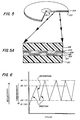
- FIGS. 1B and 2B Shown in Figures 1B and 2B are schematic representations of relative reflectivity versus temperature history observations.
- the as-deposited state is a disordered state, represented in Figure 1A and 2A by "Alpha (as deposited)", and in Figures 1B and 2B as “R AL p HA (as deposited)" and having a low reflectivity, e.g., less than 30 percent, and a high transmissivity, e.g., above about 5 percent.
- This disordered material having a crystallization temperature represented by "Txo” is converted to an ordered material, and having a higher reflectivity, e.g. above about 30 percent and a lower transmissivity, e.g., less than about 2 percent, by a pulse of energy represented by the dashed line "Ordering Pulse" in Figures 1A through 2B.
- the ordering pulse is energetic enough, that is, it has a high enough energy density and power density, to raise the temperature of the memory material within the memory cell above the crystallization temperature, Tx o , for a time sufficient to allow crystallization with minimum phase separation, but not energetic enough, that is, not having a high enough energy density or power density, to melt the material.
- an ordering pulse is meant a pulse energetic enough to raise the temperature of the memory material within a relevant volume, e.g., an individual memory cell, above its crystallization temperature, Tx, but not energetic enough to raise it above its melting temperature, T melt .
- formation may be by a three pulse "ordering pulse"-"disordering pulse”-"ordering pulse” sequence shown in Figurs 1A and 1B, which may be repeated, or by a single pulse, shown in Figures 2A and 2B.
- the disordered material having a reflectivity "R ALPHA (as deposited)" is crystallized to an ordered state having a crystallization temperature "Tx.” and a reflectivity "R o (predarkened ordered state)".
- the ordered memory material having reflectivity "R o (predarkened ordered state)” is then converted to a disordered state having a reflectivity "R AL p HA ("1" or vitreous state)”. Conversion is accomplished by subjecting the ordered material to one or more disordering pulses, represented in Figures 1A and 1B as "Disordering Pulse".
- the disordering pulse or pulses are energetic enough, i.e., has a high enough energy density and power density, to raise the temperature of the memory cell or cells above the melting temperature thereof.
- a “disordering pulse” is meant a pulse that melts ordered material under conditions where the molten material solidifies to a less ordered material.
- the molten memory material quickly cools and solidifies, i.e., vitrifies, forming a disordered material having a reflectivity R AL p HA -
- This resulting disordered state, corresponding to binary "1” is represented by “ALPHA (as vitrified)" in Figure 1A and "R AL p HA ("1" or vitreous state)" in Figure 1B.
- the disordered material may be a material having a crystallization temperature, Tx i , below that of the as-deposited, disordered material, Tx o .
- the disordered material may be a material having a crystallization temperature, T X2 , above that of the as-deposited material, Tx o .
- the disordered material may contain inclusions, regions, and/or zones of low crystallization temperature, Tx 1 , material, and of high crystallization temperature T X2 , material.
- the disordered material corresponds to binary "1" and has a reflectivity R ALPHA . It is "erased”, i.e., converted to an ordered state corresponding to binary "0", with reflectivity R, by an erasing pulse.
- the erasing pulse represented by "Erase Pulse” in Figures 1A and 1B, is an ordering pulse having sufficient energy to convert at least some of the disordered memory material in a relevant volume to ordered material.
- an “erase” pulse is an ordering pulse for converting disordered material to ordered material while avoiding formation of molten material.
- the energy pulse for erasing i.e., for converting disordered material to ordered material, should be energetic enough, i.e., should have a high enough energy density and a high enough power density, to crystallize the disordered material, but should have a low enough energy, i.e., a low enough energy density and/or a low enough power density, to avoid melting the material, to avoid the formation of crystallites having a size above about 150 angstroms, and to minimize or even avoid undesirable phase separation.
- the "erase” pulse may need to be higher than the "ordering” pulse.
- the "writing pulse” may have to be more energetic than the "disordering pulse”.
- the as deposited, disorder material having a crystallization temperature represented by Txo in Figure 2A and an as deposited reflectivity represented by "R AL p HA (as deposited)" in Figure 2B, may be directly formed to an ordered material, corresponding to a binary "0" state by application of an "ordering pulse".
- the optical data storage device herein contemplated is exemplified by optical disk means shown in Figures 3 and 4.
- the device 11 shown in Figure 3 has a rigid substrate 13 supporting at least an encapsulated phase-changeable optical data storage material 21.
- Data is stored in individual memory cells or bits in the data storage material 21.
- the individual memory cells are arrayed along parallel tracks, with the cells about 0,7 pm to 4 ⁇ m apart measured center to center along a track, and the tracks being about 1 micron to 4 microns apart.
- An individual memory cell typically has a surface area of 0,5 ⁇ m 2 to 4 ⁇ m 2 , and utilizes about 0,7 to 12 ⁇ m 2 of surface area.
- the phase-changeable optical data storage material 21 is operatively encapsulated between an anti-ablation coating 19 and a reflective coating 25.
- the anti-ablation coating 19 is between the projected energy beam and the phase: change optical data storage material 21.
- the reflective coating 23 is on the opposite side of the phase-changeaable optical data storage material 21, between the phase-changeable optical data storage material 21 and the substrate 13.
- the tri-layer of the anti-ablation coating 19, the phase-changeable optical data storage media memory 21 and the reflective coating 23 may be further encapsulated between an external transparent protective layer 18 and the substrate 13.
- the anti-ablation coating 19 enhances the conversion of projected beam energy, for example, optical energy to thermal energy, inhibits the tendency for pits or ablations to form in phase-changeable optical data storage material 21, and is substantially transparent to the projected beam erasing, reading and writing pulses.
- the anti-ablation coating 19 is formed of a dielectric material that is a thermal insulator. Exemplary materials are silicon dioxide and germanium dioxide.
- the thickness of the anti-ablation coating is on the order of the laser wavelength or an even harmonic thereof, i.e., the wavelength divided by 2n where n is from 1 to 10.
- the thickness of the anti-ablation coating is from about 0,1 to 0,5 ⁇ m but is optimized with the thickness of the phase-changeable memory material layer 21 and the reflective layer or coating 23 to optimize the energy relationships within the optical data storage device 11.
- the dielectric film 22 is positioned between the transparent encapsulating film 18 and anti-ablation coating 19.
- the reflective coating 23 e.g., a dielectric coating, as an aluminum oxide coating, or a germanium oxide coating, has a thickness of about 10 nm to about 2 pm.
- the reflective coating 23 enhances the optical efficiency of the phase-changeable optical data storage material 21.
- thermal barrier 24 on the opposite side of the optical data storage material 21 between the optical data storage material 21 and the reflector 23 to enhance the conversion of the particle beam energy to thermal energy.
- the thermal barrier 24 is from about 0.1 micron to about 20 microns thick and is formed of silicon dioxide or of germanium oxide.
- the encapsulant transparent film 18 provides protection from the environment, especially from water and water vapor, and is typically a transparent metal oxide or an organic polymer, for example, polymethylmethacrylate or the like. Additionally, a subbing layer formed, for example, of polymethylmethacrylate, may be provided between the substrate and the thermal barrier.
- the anti-ablation coating 19, the optical data storage material 21, the transparent dielectric 22 (when present), reflective layer 23 and the thermal barrier 24 (when present) are optically coupled and optimized. That is, the thicknesses and optical properties of the layers are optimized so as to optimize anti-reflective properties, favor high reflection in the read mode, and high absorption in the "erase" and "write” modes. Where the optical coupling or optimization is thusly optimized, the total energy applied is reduced.
- an optical data storage device 111 having a substrate 113 with a reflective, thermally insulating film, coating or layer 124 of an oxide, for example, germanium oxide, tellurium oxide or the like.
- the insulating, reflective layer 124 is from about 0,1 to about 0,5 um thick.
- Above the reflective, insulating layer 124 is a phase-changeable optical data storage material 121 having a thickness of from about 50 to about 200 nm thick.
- a layer 119 of an anti-ablation, anti-reflective material 119 is provided above the layer 121 of optical data storage material.
- the anti-ablation, anti-reflective coating 119 is also formed of a transparent dielectric, as a metal oxide or other metal compound such as germanium oxide, and has a thickness of about 0,1 to about 0,3 pm. Bonded thereto by an adhesive resin film 120 is an encapsulating, encapsulating polymeric layer, 118 e.g. of polymethylmethacrylate, about 0,25 to about 2 nm.
- the layer of optical data storage material 21, 121 is from about 5 nm to about 2 pm thick and especially from about 50 nm to about 200 nm thick and in a particularly preferred exemplification from about 70 to about 150 nm thick.
- phase-changeable material 21, 121, 221 is reversible with the absence of topographic change on phase change and has a signal to noise ratio above about 40 decibels and preferably above about 50 or more decibels.
- the phase-changeable material 21, 121, 221 is phase-changeable between a plurality of detectable states, that is between two or more detectable states, exemplified by a disordered or amorphous state and an ordered state, or between relative degrees of localized order which are detectable.
- the stable detectable states of the phase-changeable optical data storage material 21, 121, 221 may be optically detectable as by reflectivity, refractivity, absorbency, or transmissivity. Alternatively, they may be electrically detectable as by resistance or capacitance.
- a data storage device 211 for example an optical data storage disc, as shown in Figure 5 and 5A.
- the disc is adapted for use with a projected beam energy source, e.g., a laser.
- the device 211 has two substrates 213, 218.
- the substrates 213, 218, are formed of a transparent material, e.g., a polymeric material such as polymethyl methacrylate.
- Atop the substrate 213 is a layer 231, e.g. a photoinitiated, polymerized acrylic layer. Polymerized, molder or cast into the photopolymer layer 231 are concentric grooves.
- the grooves have a depth represented by the function A/8, where ⁇ is the wavelength of the incident energy, e.g., about 90 nm, a width in the valleys of from about 1,5 to about 2,5 pm, and preferably about 2,0 ⁇ m, a width on the lands of from about 0,5 to about 0,7 pm, and preferably about 0,5 ⁇ m and a pitch of from about 2,0 to about 3,2 pm and preferably about 2,5 pm.
- the active materials e.g., a multilayer of inorganic encapsulant 223, the active state change material 221, and a second layer of inorganic encapsulant 219, are present between the two substrates 213, 218.
- Inorganic encapsulant layer 219 adheres to substrate 218 with adhesive layer 233.
- the adhesive layer 233 and the layers 219, 221, 223 conform to the grooves in the grooved photopolymer layer 231.
- the layers 231, 233 are formed of photo-initiated polymers, e.g., photopolymers. Typical photopolymers include acrylates and epoxides.
- the grooved layer 231 adheres to the first substrate 213.
- the adhesive layer 233 is adherent to the second substrate 218.
- the adhesive layer 233 is about 100 nm to about 100 ⁇ m thick, and the grooved layer 231 is about 50 to about 250 nm thick.
- the active portion of the device 211 includes the first encapsulant layer 223, the layer of active state changeable memory material 221, and the second encapsulant layer 219.
- the encapsulant layers 219, 223 are from about 150 to about 250 nm thick.
- the layer of active, state change material 221 is from about 50 to about 200 nm thick.
- the encapsulant layers 219, 223 may be single layers or multiple layers.
- the encapsulant is typically a dielectric, exemplified by germanium oxide.
- the active state change material is a chalcogenide.
- one of the set of lands or of valleys is in an ordered state, e.g., a crystalline state.
- the set of lands or of valleys is converted to the relatively ordered state by the herein contemplated process and is generally not substantially vitrified by subsequent order-disorder or erase-write cycles.
- the materials useful for providing these phase-changeable optical data storage materials 21,121, 221 are materials where a phase-change with detectable properties occur.
- the states corresponding to the detectable properties are stable at the temperatures encountered in storage and operation.
- the materials are chalcogenides, e.g., tellurium based alloys, and they may be present as metals, as oxides, including nonstoichiometric oxides and other compounds, compositions and alloys thereof.
- the chalcogenide consists of tellurium alloyed with other components such as oxygen, sulfur, selenium, elements of Group IIIB, metals and semi-metals of Group IVB, semi-metals of Group VB, low melting point metals, and the like.
- the chalcogenides, tellurium, tellurium-selenium alloys, and the like, and combinations thereof can have Group IIIB elements present therewith.
- Typical Group IIIB additive components and additives include boron, aluminum, gallium and indium.
- the chalcogenides, tellurium, tellurium-selenium alloys, and combinations thereof, may be combined with the metals and semi-metals of Group IVB including carbon, silicon, germanium, tin, lead and combinations thereof.
- Useful Group VB additive components include nitrogen, phosphorous, arsenic, antimony and bismuth.
- Combinations of Group IVB adducts and other additive components may be present as a chalcogenide with (1) silicon, germanium, tin, lead or combinations thereof and (2) one or more additive components chosen from the Group consisting of (a) Group IIIB components, (b) Group VB components and (c) combinations thereof.
- Typical combinations of Group IIIB and Group VB additive components include gallium arsenide and indium antimonide. Other combinations include (1) tellurium-germanium, (2) tellurium-germanium with gallium arsenide, (3) tellurium-germanium with gallium arsenide and iron, (4) tellurium-antimony, and (5) tellurium-lead.
- the above compounds, compositions, and alloys may also include oxygen, sulfur, or oxygen and sulfur, and may be present in the form of oxides, subox- ides, sulfides, subsulfides, oxysulfides and sub- oxysulfides, as well as other nonstoichiometric compounds.
- the chalcogenides or the oxides or sulfides thereof may be present with the transition metal additives, either as the metal or the oxide, or the sulfide, for example, vanadium, chromium, manganese, iron, cobalt, tungsten, titanium and the like.
- the layer of optical data storage material 21, 121, 221 may be deposited by various techniques that result in the formation of a relatively disordered material. These include evaporation and various plasma processes. Exemplary plasma processes include sputtering where the deposit is introduced as a solid and deposited from an alloy target, cosputtered from multiple targets and/or reactively sputtered or cosputtered with a gas. Alternatively, the plasma process may be glow discharge process as is well known in the art and described in U.S. Patent 4,226,898 and 4,217,374. The plasma process may be a d.c. process, a biased d.c. process, a radio frequency biased process, or a microwave process.
- the above processes result in an as-deposited layer 21, 121, 221 that is disordered. That is, the material in the layer is characterized by the substantial absence of long range order and the presence of long range disorder, although short range, nearest neighbor atomic order may be present within the deposit.
- the "as-deposited" morphology of the optical storage data material 21, 121, 221 differs from the morphology of the material obtained by converting a crystalline or ordered material to a disordered state by the application of energy thereto: That is, for data entry purposes, the disordered state corresponding to the binary number 1 (where the more ordered state corresponds to the binary number 0) may be different from the as-deposited disordered state. It is therefore necessary to utilize the method described herein to convert the as-deposited material to a more ordered material. The conversion of the as-deposited material is carried out during the manufacturing process by the application of energy thereto under conditions that do not result in ablation or change to the topography.
- This may be carried out after the encapsulation of material, for example, after deposition or formation of the anti-reflective, thermally insulating, dielectric, and atmospheric sealing encapsulant layers.
- formation may be carried out at an earlier stage in the manufacturing process, for example, in situ, in the deposition chamber immediately after deposition of the optical data storage material layer 21, 121, 221 and before any subsqeuent layer thereon.
- the optical data storage device having incorporated therein an optical data storage medium 21, 121, 221 switchable between at least two detectable states, as described hereinabove, by the application of projected beam energy thereto, is present in the device 11, 111, 211 in an as-deposited, first, disordered state prior to formation.
- Formation comprises the step of simultaneously applying a single, ordering energy pulse to many memory cells, and preferably to the entire surface of the data storage material 21, 121, 221, whereby to convert the optical data storage medium 21, 121, 221 from the as-deposited disordered state to a more ordered state.
- a disordering energy pulse may be applied to the optical data storage medium 21, 121, 221 which converts the optical data storage medium from an intermediate ordered state to a second disordered state, e.g., a disordered state different from the as-deposited disordered state.
- the disordering pulse is followed by a second ordering energy pulse to convert the second disordered state to an ordered state having reflectivity "R i ("o", formed, ordered state)" as shown in Figure 1B.
- the ordering energy pulses have an energy from about 0,1 to about 1 joule per square centimeter.
- the ordering energy pulses are applied to the optical data storage medium for an interval of from about 0,1 to 100 psec. Shorter durations of pulse do not result in substantially complete or satisfactory conversion to an ordered state, while longer duration pulses may result in substantial phase separation during crystallization.
- the ordering pulses are either monochromatic or non-monochromatic energy pulses.
- FIG. 6 is a graph of reflectivity versus number of cycles for an optical data storage device where the forming pulse, i.e., the ordering pulse is applied by a xenon flash lamp force, and the disordering pulse is applied by a YAG laser.
- the relatively ordered optical data storage material 21, 121, 221 formed by the ordering of the as-deposited optical data storage material is the formed state.
- an optical data storage device is prepared on a grooved, blank substrate by the reactive sputtering of germanium in the presence of oxygen to form a germanium oxide film of about 70 to 150 nm thick atop a thin film of polymethol methacrylate. Atop this film, there is formed a tellurium-tin-germanium oxygen film of from about70 to about 150 nm thick by the reactive cosputtering of germanium, tellurium and tin in the presence of an oxygen atmosphere. Atop the 70 to 150 nm thick film of the phase-changeable material is applied a film of a germanium oxide film of about 150 to about 300 nm thick by reactive sputtering. Atop this film, an adhesive layer of about 0,05 to about 0,2 mm thick is applied and a polymethylmethacrylate plate of about 0,5 to about 2 mm thick is applied as an encapsulant.
- the layer of tellurium-germanium-tin oxide, as sputtered, is in a disordered state having a reflectivity of 21% and an optical transmissivity of 10 percent.
- This layer is converted to a relatively more ordered state by the application of the projected beam energy by a xenon discharge lamp having an energy of about 0.5 joule per square centimeter, and a flash duration of about 50 microseconds.
- the resulting ordered state characterized as "predarkened", has a reflectivity of 39% and an optical transmissivity of 2%.
- the resulting ordered layer of optical data storage medium is then converted to a second, disordered state different from the deposited disordered state by the application of energy thereto from a YAG laser having an energy density of about 20 to about 50 millijoules per square centimeter, and a flash duration of about 15 nsec.
- the resulting disordered material has a reflectivity of 24% and an optical transmissivity of 7%.
- the disordered material is crystallized to a "formed" state, i.e., an "erased” state, by the application of a 0.6 joules per square centimeter xenon flash lamp having a duration of 50 microseconds.
- the resulting "initial" state has a reflectivity of 43% and an optical transmissivity of 1%. This is shown in Figure 6.
Landscapes
- Engineering & Computer Science (AREA)
- Manufacturing & Machinery (AREA)
- Thermal Transfer Or Thermal Recording In General (AREA)
- Optical Record Carriers And Manufacture Thereof (AREA)
Claims (14)
dadurch gekennzeichnet, daß das erste im wesentlichen lichtdurchlässige Substrat (213) von einer Haftschicht (231) überdeckt ist, die Stege und Vertiefungen bildet und ein Polymer umfaßt, das ein Polyacrylat oder Polyepoxid ist, und daß die Speicherschicht (221) ein Chalkogenidmaterial aufweist, das wenigstens eine Gruppe von Vertiefungen und Stegen bildet, die nach der Bildung im wesentlichen kristallin sind.
Applications Claiming Priority (4)
| Application Number | Priority Date | Filing Date | Title |
|---|---|---|---|
| US66729484A | 1984-11-01 | 1984-11-01 | |
| US769227 | 1985-08-26 | ||
| US06/769,227 US4719594A (en) | 1984-11-01 | 1985-08-26 | Grooved optical data storage device including a chalcogenide memory layer |
| US667294 | 2000-09-22 |
Publications (3)
| Publication Number | Publication Date |
|---|---|
| EP0180103A2 EP0180103A2 (de) | 1986-05-07 |
| EP0180103A3 EP0180103A3 (en) | 1986-08-20 |
| EP0180103B1 true EP0180103B1 (de) | 1989-10-04 |
Family
ID=27099656
Family Applications (1)
| Application Number | Title | Priority Date | Filing Date |
|---|---|---|---|
| EP85113183A Expired EP0180103B1 (de) | 1984-11-01 | 1985-10-17 | Verfahren zur Herstellung einer optischen Datenspeicherungsvorrichtung und die dadurch hergestellte optische Datenspeicherungsvorrichtung |
Country Status (6)
| Country | Link |
|---|---|
| US (1) | US4719594A (de) |
| EP (1) | EP0180103B1 (de) |
| KR (1) | KR940000420B1 (de) |
| AU (1) | AU574855B2 (de) |
| CA (1) | CA1244943A (de) |
| DE (1) | DE3573484D1 (de) |
Families Citing this family (218)
| Publication number | Priority date | Publication date | Assignee | Title |
|---|---|---|---|---|
| US4825408A (en) * | 1984-04-25 | 1989-04-25 | The Johns Hopkins University | Multistate optical switching and memory apparatus using an amphoteric organic charge transfer material |
| US4653024A (en) * | 1984-11-21 | 1987-03-24 | Energy Conversion Devices, Inc. | Data storage device including a phase changeable material |
| CN1008845B (zh) * | 1984-12-05 | 1990-07-18 | 富士通株式会社 | 光学信息记录介质及信息的记录与擦抹的方法 |
| JPH0695404B2 (ja) * | 1985-12-27 | 1994-11-24 | ソニー株式会社 | 光磁気記録方法 |
| JPS63171446A (ja) * | 1987-01-09 | 1988-07-15 | Mitsubishi Kasei Corp | 光学的記録用媒体の製造方法 |
| US4797871A (en) * | 1986-09-15 | 1989-01-10 | Eastman Kodak Company | Erasable optical recording method |
| US5339301A (en) * | 1986-10-06 | 1994-08-16 | U.S. Philips Corporation | Optically readable record carrier for recording information, method and apparatus for manufacturing such, apparatus for recording and reading information on a such a record carrier |
| GB8701411D0 (en) * | 1987-01-22 | 1987-02-25 | Emi Plc Thorn | Storage media |
| US4900691A (en) * | 1987-04-17 | 1990-02-13 | Kanegafuchi Chemical Industry Company, Limited | Method of fabrication for optical storage apparatus |
| US4855950A (en) * | 1987-04-17 | 1989-08-08 | Kanegafuchi Chemical Industry Company, Limited | Optical storage apparatus including a reversible, doping modulated, multilayer, amorphous element |
| US5257256A (en) * | 1987-04-24 | 1993-10-26 | Hitachi, Ltd. | Recording waveform for mark-length modulation optical recording |
| JP2702923B2 (ja) * | 1987-04-24 | 1998-01-26 | 株式会社日立製作所 | 情報の記録方法及び情報記録装置 |
| US4924436A (en) * | 1987-06-22 | 1990-05-08 | Energy Conversion Devices, Inc. | Data storage device having a phase change memory medium reversible by direct overwrite and method of direct overwrite |
| US4876667A (en) * | 1987-06-22 | 1989-10-24 | Energy Conversion Devices, Inc. | Data storage device having a phase change memory medium reversible by direct overwrite |
| GB8804994D0 (en) * | 1988-03-02 | 1988-03-30 | Guiver T G | Protective element for laser disc & method of applying same |
| EP0337553B1 (de) * | 1988-04-13 | 1993-12-01 | Koninklijke Philips Electronics N.V. | Laminiertes Produkt, Verbindung zur Verwendung in dem laminierten Produkt und optischer Informationsspeicher, versehen mit dem laminierten Produkt |
| US5294523A (en) * | 1988-08-01 | 1994-03-15 | Matsushita Electric Industrial Co., Ltd. | Optical information recording medium |
| US5056079A (en) * | 1988-08-04 | 1991-10-08 | Literal Corporation | Multi-state optical contrasts in optical recording media for data compression |
| EP0405605B1 (de) * | 1989-06-30 | 1998-07-29 | Fuji Xerox Co., Ltd. | Medium und Verfahren zur optischen Aufzeichnung |
| WO1991005342A1 (en) * | 1989-09-28 | 1991-04-18 | Matsushita Electric Industrial Co., Ltd. | Optical data recording medium and method of producing the same |
| US5242784A (en) * | 1990-07-13 | 1993-09-07 | International Business Machines Corporation | System and method for optical phase change recording |
| US5368986A (en) * | 1991-05-02 | 1994-11-29 | Hitachi, Ltd. | Information recording media, manufacturing method for the same, and information recording method |
| US5373491A (en) * | 1991-05-30 | 1994-12-13 | Hitachi, Ltd. | Wavelength-multiple optical recording medium |
| US5234803A (en) * | 1992-05-21 | 1993-08-10 | Eastman Kodak Company | Optical recording media |
| EP1006518B1 (de) * | 1994-09-27 | 2004-03-17 | Matsushita Electric Industrial Co., Ltd. | Verfahren zur Herstellung eines optischen Informationsaufzeichnungsmediums und Gerät dazu |
| EP0706179B1 (de) * | 1994-09-27 | 2002-12-11 | Matsushita Electric Industrial Co., Ltd. | Verfahren zur Herstellung eines optischen Informationsaufzeichnungsmediums und Gerät dazu |
| US7260051B1 (en) * | 1998-12-18 | 2007-08-21 | Nanochip, Inc. | Molecular memory medium and molecular memory integrated circuit |
| US6900468B2 (en) * | 2001-02-20 | 2005-05-31 | Hewlett-Packard Development Company, L.P. | Indium chalcogenide, gallium chalcogenide, and indium-gallium chalcogenide phase-change media for ultra-high-density data-storage devices |
| US20020138301A1 (en) * | 2001-03-22 | 2002-09-26 | Thanos Karras | Integration of a portal into an application service provider data archive and/or web based viewer |
| US7300690B2 (en) * | 2001-03-29 | 2007-11-27 | General Electric Company | Radial tilt reduced media |
| US6716505B2 (en) * | 2001-08-31 | 2004-04-06 | General Electric Company | Storage medium for data with improved dimensional stability |
| US20030128646A1 (en) * | 2002-01-09 | 2003-07-10 | Peter Nangle | Asymmetrical programming mechanism for non-volatile memory |
| US6579760B1 (en) * | 2002-03-28 | 2003-06-17 | Macronix International Co., Ltd. | Self-aligned, programmable phase change memory |
| US6864503B2 (en) * | 2002-08-09 | 2005-03-08 | Macronix International Co., Ltd. | Spacer chalcogenide memory method and device |
| US6850432B2 (en) | 2002-08-20 | 2005-02-01 | Macronix International Co., Ltd. | Laser programmable electrically readable phase-change memory method and device |
| US6985377B2 (en) * | 2002-10-15 | 2006-01-10 | Nanochip, Inc. | Phase change media for high density data storage |
| US7233517B2 (en) | 2002-10-15 | 2007-06-19 | Nanochip, Inc. | Atomic probes and media for high density data storage |
| US7115927B2 (en) | 2003-02-24 | 2006-10-03 | Samsung Electronics Co., Ltd. | Phase changeable memory devices |
| US7402851B2 (en) * | 2003-02-24 | 2008-07-22 | Samsung Electronics Co., Ltd. | Phase changeable memory devices including nitrogen and/or silicon and methods for fabricating the same |
| US7244813B2 (en) * | 2003-08-26 | 2007-07-17 | General Electric Company | Methods of purifying polymeric material |
| US20050046056A1 (en) * | 2003-08-26 | 2005-03-03 | Jiawen Dong | Method of molding articles |
| US20050048252A1 (en) * | 2003-08-26 | 2005-03-03 | Irene Dris | Substrate and storage media for data prepared therefrom |
| US7354990B2 (en) * | 2003-08-26 | 2008-04-08 | General Electric Company | Purified polymeric materials and methods of purifying polymeric materials |
| US7041780B2 (en) * | 2003-08-26 | 2006-05-09 | General Electric | Methods of preparing a polymeric material composite |
| US7301887B2 (en) * | 2004-04-16 | 2007-11-27 | Nanochip, Inc. | Methods for erasing bit cells in a high density data storage device |
| US20050243660A1 (en) * | 2004-04-16 | 2005-11-03 | Rust Thomas F | Methods for erasing bit cells in a high density data storage device |
| US20050232061A1 (en) | 2004-04-16 | 2005-10-20 | Rust Thomas F | Systems for writing and reading highly resolved domains for high density data storage |
| US7379412B2 (en) | 2004-04-16 | 2008-05-27 | Nanochip, Inc. | Methods for writing and reading highly resolved domains for high density data storage |
| US20050243592A1 (en) * | 2004-04-16 | 2005-11-03 | Rust Thomas F | High density data storage device having eraseable bit cells |
| JP4529654B2 (ja) * | 2004-11-15 | 2010-08-25 | ソニー株式会社 | 記憶素子及び記憶装置 |
| US20060108667A1 (en) * | 2004-11-22 | 2006-05-25 | Macronix International Co., Ltd. | Method for manufacturing a small pin on integrated circuits or other devices |
| US7220983B2 (en) * | 2004-12-09 | 2007-05-22 | Macronix International Co., Ltd. | Self-aligned small contact phase-change memory method and device |
| US7709334B2 (en) | 2005-12-09 | 2010-05-04 | Macronix International Co., Ltd. | Stacked non-volatile memory device and methods for fabricating the same |
| JP4815804B2 (ja) * | 2005-01-11 | 2011-11-16 | ソニー株式会社 | 記憶素子及び記憶装置 |
| US7534647B2 (en) | 2005-06-17 | 2009-05-19 | Macronix International Co., Ltd. | Damascene phase change RAM and manufacturing method |
| US8237140B2 (en) * | 2005-06-17 | 2012-08-07 | Macronix International Co., Ltd. | Self-aligned, embedded phase change RAM |
| US7598512B2 (en) * | 2005-06-17 | 2009-10-06 | Macronix International Co., Ltd. | Thin film fuse phase change cell with thermal isolation layer and manufacturing method |
| US7321130B2 (en) * | 2005-06-17 | 2008-01-22 | Macronix International Co., Ltd. | Thin film fuse phase change RAM and manufacturing method |
| US7238994B2 (en) | 2005-06-17 | 2007-07-03 | Macronix International Co., Ltd. | Thin film plate phase change ram circuit and manufacturing method |
| US7696503B2 (en) * | 2005-06-17 | 2010-04-13 | Macronix International Co., Ltd. | Multi-level memory cell having phase change element and asymmetrical thermal boundary |
| US7514367B2 (en) * | 2005-06-17 | 2009-04-07 | Macronix International Co., Ltd. | Method for manufacturing a narrow structure on an integrated circuit |
| US7514288B2 (en) * | 2005-06-17 | 2009-04-07 | Macronix International Co., Ltd. | Manufacturing methods for thin film fuse phase change ram |
| US20060291271A1 (en) * | 2005-06-24 | 2006-12-28 | Nanochip, Inc. | High density data storage devices having servo indicia formed in a patterned media |
| US7367119B2 (en) * | 2005-06-24 | 2008-05-06 | Nanochip, Inc. | Method for forming a reinforced tip for a probe storage device |
| US7463573B2 (en) * | 2005-06-24 | 2008-12-09 | Nanochip, Inc. | Patterned media for a high density data storage device |
| US20070008867A1 (en) * | 2005-07-08 | 2007-01-11 | Nanochip, Inc. | High density data storage devices with a lubricant layer comprised of a field of polymer chains |
| US7309630B2 (en) * | 2005-07-08 | 2007-12-18 | Nanochip, Inc. | Method for forming patterned media for a high density data storage device |
| US20070008866A1 (en) * | 2005-07-08 | 2007-01-11 | Nanochip, Inc. | Methods for writing and reading in a polarity-dependent memory switch media |
| US20070008865A1 (en) * | 2005-07-08 | 2007-01-11 | Nanochip, Inc. | High density data storage devices with polarity-dependent memory switching media |
| KR100637235B1 (ko) * | 2005-08-26 | 2006-10-20 | 삼성에스디아이 주식회사 | 플라즈마 디스플레이 패널 |
| US8155312B2 (en) * | 2005-10-18 | 2012-04-10 | The University Of Connecticut | Optical data storage device and method |
| US7397060B2 (en) * | 2005-11-14 | 2008-07-08 | Macronix International Co., Ltd. | Pipe shaped phase change memory |
| US20070111429A1 (en) * | 2005-11-14 | 2007-05-17 | Macronix International Co., Ltd. | Method of manufacturing a pipe shaped phase change memory |
| US7635855B2 (en) * | 2005-11-15 | 2009-12-22 | Macronix International Co., Ltd. | I-shaped phase change memory cell |
| US7450411B2 (en) | 2005-11-15 | 2008-11-11 | Macronix International Co., Ltd. | Phase change memory device and manufacturing method |
| US7786460B2 (en) * | 2005-11-15 | 2010-08-31 | Macronix International Co., Ltd. | Phase change memory device and manufacturing method |
| US7394088B2 (en) * | 2005-11-15 | 2008-07-01 | Macronix International Co., Ltd. | Thermally contained/insulated phase change memory device and method (combined) |
| US7414258B2 (en) | 2005-11-16 | 2008-08-19 | Macronix International Co., Ltd. | Spacer electrode small pin phase change memory RAM and manufacturing method |
| US7479649B2 (en) * | 2005-11-21 | 2009-01-20 | Macronix International Co., Ltd. | Vacuum jacketed electrode for phase change memory element |
| TWI318003B (en) * | 2005-11-21 | 2009-12-01 | Macronix Int Co Ltd | Air cell thermal isolation for a memory array formed of a programmable resistive material |
| US7829876B2 (en) * | 2005-11-21 | 2010-11-09 | Macronix International Co., Ltd. | Vacuum cell thermal isolation for a phase change memory device |
| US7449710B2 (en) * | 2005-11-21 | 2008-11-11 | Macronix International Co., Ltd. | Vacuum jacket for phase change memory element |
| US7507986B2 (en) | 2005-11-21 | 2009-03-24 | Macronix International Co., Ltd. | Thermal isolation for an active-sidewall phase change memory cell |
| US7599217B2 (en) | 2005-11-22 | 2009-10-06 | Macronix International Co., Ltd. | Memory cell device and manufacturing method |
| US7459717B2 (en) * | 2005-11-28 | 2008-12-02 | Macronix International Co., Ltd. | Phase change memory cell and manufacturing method |
| US7688619B2 (en) | 2005-11-28 | 2010-03-30 | Macronix International Co., Ltd. | Phase change memory cell and manufacturing method |
| US7521364B2 (en) | 2005-12-02 | 2009-04-21 | Macronix Internation Co., Ltd. | Surface topology improvement method for plug surface areas |
| US7605079B2 (en) * | 2005-12-05 | 2009-10-20 | Macronix International Co., Ltd. | Manufacturing method for phase change RAM with electrode layer process |
| US7642539B2 (en) * | 2005-12-13 | 2010-01-05 | Macronix International Co., Ltd. | Thin film fuse phase change cell with thermal isolation pad and manufacturing method |
| GB2433647B (en) | 2005-12-20 | 2008-05-28 | Univ Southampton | Phase change memory materials, devices and methods |
| US7531825B2 (en) | 2005-12-27 | 2009-05-12 | Macronix International Co., Ltd. | Method for forming self-aligned thermal isolation cell for a variable resistance memory array |
| US8062833B2 (en) * | 2005-12-30 | 2011-11-22 | Macronix International Co., Ltd. | Chalcogenide layer etching method |
| US7560337B2 (en) | 2006-01-09 | 2009-07-14 | Macronix International Co., Ltd. | Programmable resistive RAM and manufacturing method |
| US7595218B2 (en) * | 2006-01-09 | 2009-09-29 | Macronix International Co., Ltd. | Programmable resistive RAM and manufacturing method |
| US7741636B2 (en) * | 2006-01-09 | 2010-06-22 | Macronix International Co., Ltd. | Programmable resistive RAM and manufacturing method |
| US20070158632A1 (en) * | 2006-01-09 | 2007-07-12 | Macronix International Co., Ltd. | Method for Fabricating a Pillar-Shaped Phase Change Memory Element |
| US7825396B2 (en) * | 2006-01-11 | 2010-11-02 | Macronix International Co., Ltd. | Self-align planerized bottom electrode phase change memory and manufacturing method |
| US7432206B2 (en) * | 2006-01-24 | 2008-10-07 | Macronix International Co., Ltd. | Self-aligned manufacturing method, and manufacturing method for thin film fuse phase change ram |
| US7456421B2 (en) * | 2006-01-30 | 2008-11-25 | Macronix International Co., Ltd. | Vertical side wall active pin structures in a phase change memory and manufacturing methods |
| US7956358B2 (en) * | 2006-02-07 | 2011-06-07 | Macronix International Co., Ltd. | I-shaped phase change memory cell with thermal isolation |
| US7910907B2 (en) * | 2006-03-15 | 2011-03-22 | Macronix International Co., Ltd. | Manufacturing method for pipe-shaped electrode phase change memory |
| US7554144B2 (en) * | 2006-04-17 | 2009-06-30 | Macronix International Co., Ltd. | Memory device and manufacturing method |
| US7928421B2 (en) | 2006-04-21 | 2011-04-19 | Macronix International Co., Ltd. | Phase change memory cell with vacuum spacer |
| US8129706B2 (en) * | 2006-05-05 | 2012-03-06 | Macronix International Co., Ltd. | Structures and methods of a bistable resistive random access memory |
| US7608848B2 (en) * | 2006-05-09 | 2009-10-27 | Macronix International Co., Ltd. | Bridge resistance random access memory device with a singular contact structure |
| KR100782482B1 (ko) * | 2006-05-19 | 2007-12-05 | 삼성전자주식회사 | GeBiTe막을 상변화 물질막으로 채택하는 상변화 기억 셀, 이를 구비하는 상변화 기억소자, 이를 구비하는 전자 장치 및 그 제조방법 |
| US7423300B2 (en) | 2006-05-24 | 2008-09-09 | Macronix International Co., Ltd. | Single-mask phase change memory element |
| US7820997B2 (en) * | 2006-05-30 | 2010-10-26 | Macronix International Co., Ltd. | Resistor random access memory cell with reduced active area and reduced contact areas |
| US7732800B2 (en) * | 2006-05-30 | 2010-06-08 | Macronix International Co., Ltd. | Resistor random access memory cell with L-shaped electrode |
| US20080001075A1 (en) * | 2006-06-15 | 2008-01-03 | Nanochip, Inc. | Memory stage for a probe storage device |
| US7696506B2 (en) | 2006-06-27 | 2010-04-13 | Macronix International Co., Ltd. | Memory cell with memory material insulation and manufacturing method |
| US7785920B2 (en) * | 2006-07-12 | 2010-08-31 | Macronix International Co., Ltd. | Method for making a pillar-type phase change memory element |
| US7442603B2 (en) * | 2006-08-16 | 2008-10-28 | Macronix International Co., Ltd. | Self-aligned structure and method for confining a melting point in a resistor random access memory |
| US7772581B2 (en) | 2006-09-11 | 2010-08-10 | Macronix International Co., Ltd. | Memory device having wide area phase change element and small electrode contact area |
| US7504653B2 (en) * | 2006-10-04 | 2009-03-17 | Macronix International Co., Ltd. | Memory cell device with circumferentially-extending memory element |
| US7510929B2 (en) * | 2006-10-18 | 2009-03-31 | Macronix International Co., Ltd. | Method for making memory cell device |
| US20080094885A1 (en) * | 2006-10-24 | 2008-04-24 | Macronix International Co., Ltd. | Bistable Resistance Random Access Memory Structures with Multiple Memory Layers and Multilevel Memory States |
| US7527985B2 (en) | 2006-10-24 | 2009-05-05 | Macronix International Co., Ltd. | Method for manufacturing a resistor random access memory with reduced active area and reduced contact areas |
| US7388771B2 (en) * | 2006-10-24 | 2008-06-17 | Macronix International Co., Ltd. | Methods of operating a bistable resistance random access memory with multiple memory layers and multilevel memory states |
| US7863655B2 (en) * | 2006-10-24 | 2011-01-04 | Macronix International Co., Ltd. | Phase change memory cells with dual access devices |
| US8067762B2 (en) | 2006-11-16 | 2011-11-29 | Macronix International Co., Ltd. | Resistance random access memory structure for enhanced retention |
| US7473576B2 (en) * | 2006-12-06 | 2009-01-06 | Macronix International Co., Ltd. | Method for making a self-converged void and bottom electrode for memory cell |
| US7682868B2 (en) | 2006-12-06 | 2010-03-23 | Macronix International Co., Ltd. | Method for making a keyhole opening during the manufacture of a memory cell |
| US20080137400A1 (en) * | 2006-12-06 | 2008-06-12 | Macronix International Co., Ltd. | Phase Change Memory Cell with Thermal Barrier and Method for Fabricating the Same |
| US7476587B2 (en) * | 2006-12-06 | 2009-01-13 | Macronix International Co., Ltd. | Method for making a self-converged memory material element for memory cell |
| US7697316B2 (en) * | 2006-12-07 | 2010-04-13 | Macronix International Co., Ltd. | Multi-level cell resistance random access memory with metal oxides |
| US7903447B2 (en) * | 2006-12-13 | 2011-03-08 | Macronix International Co., Ltd. | Method, apparatus and computer program product for read before programming process on programmable resistive memory cell |
| US8344347B2 (en) * | 2006-12-15 | 2013-01-01 | Macronix International Co., Ltd. | Multi-layer electrode structure |
| US7718989B2 (en) * | 2006-12-28 | 2010-05-18 | Macronix International Co., Ltd. | Resistor random access memory cell device |
| US7515461B2 (en) * | 2007-01-05 | 2009-04-07 | Macronix International Co., Ltd. | Current compliant sensing architecture for multilevel phase change memory |
| US7433226B2 (en) | 2007-01-09 | 2008-10-07 | Macronix International Co., Ltd. | Method, apparatus and computer program product for read before programming process on multiple programmable resistive memory cell |
| US7440315B2 (en) | 2007-01-09 | 2008-10-21 | Macronix International Co., Ltd. | Method, apparatus and computer program product for stepped reset programming process on programmable resistive memory cell |
| US20080175033A1 (en) * | 2007-01-19 | 2008-07-24 | Nanochip, Inc. | Method and system for improving domain stability in a ferroelectric media |
| US20080174918A1 (en) * | 2007-01-19 | 2008-07-24 | Nanochip, Inc. | Method and system for writing and reading a charge-trap media with a probe tip |
| US7535756B2 (en) | 2007-01-31 | 2009-05-19 | Macronix International Co., Ltd. | Method to tighten set distribution for PCRAM |
| US7663135B2 (en) | 2007-01-31 | 2010-02-16 | Macronix International Co., Ltd. | Memory cell having a side electrode contact |
| US7619311B2 (en) * | 2007-02-02 | 2009-11-17 | Macronix International Co., Ltd. | Memory cell device with coplanar electrode surface and method |
| US7701759B2 (en) * | 2007-02-05 | 2010-04-20 | Macronix International Co., Ltd. | Memory cell device and programming methods |
| US7483292B2 (en) * | 2007-02-07 | 2009-01-27 | Macronix International Co., Ltd. | Memory cell with separate read and program paths |
| US7463512B2 (en) * | 2007-02-08 | 2008-12-09 | Macronix International Co., Ltd. | Memory element with reduced-current phase change element |
| US8138028B2 (en) * | 2007-02-12 | 2012-03-20 | Macronix International Co., Ltd | Method for manufacturing a phase change memory device with pillar bottom electrode |
| US7884343B2 (en) * | 2007-02-14 | 2011-02-08 | Macronix International Co., Ltd. | Phase change memory cell with filled sidewall memory element and method for fabricating the same |
| US7619237B2 (en) * | 2007-02-21 | 2009-11-17 | Macronix International Co., Ltd. | Programmable resistive memory cell with self-forming gap |
| US8008643B2 (en) * | 2007-02-21 | 2011-08-30 | Macronix International Co., Ltd. | Phase change memory cell with heater and method for fabricating the same |
| US7956344B2 (en) * | 2007-02-27 | 2011-06-07 | Macronix International Co., Ltd. | Memory cell with memory element contacting ring-shaped upper end of bottom electrode |
| US20080233672A1 (en) * | 2007-03-20 | 2008-09-25 | Nanochip, Inc. | Method of integrating mems structures and cmos structures using oxide fusion bonding |
| US7786461B2 (en) | 2007-04-03 | 2010-08-31 | Macronix International Co., Ltd. | Memory structure with reduced-size memory element between memory material portions |
| US8610098B2 (en) | 2007-04-06 | 2013-12-17 | Macronix International Co., Ltd. | Phase change memory bridge cell with diode isolation device |
| US7755076B2 (en) * | 2007-04-17 | 2010-07-13 | Macronix International Co., Ltd. | 4F2 self align side wall active phase change memory |
| US7569844B2 (en) * | 2007-04-17 | 2009-08-04 | Macronix International Co., Ltd. | Memory cell sidewall contacting side electrode |
| US7483316B2 (en) * | 2007-04-24 | 2009-01-27 | Macronix International Co., Ltd. | Method and apparatus for refreshing programmable resistive memory |
| US8513637B2 (en) | 2007-07-13 | 2013-08-20 | Macronix International Co., Ltd. | 4F2 self align fin bottom electrodes FET drive phase change memory |
| US7777215B2 (en) | 2007-07-20 | 2010-08-17 | Macronix International Co., Ltd. | Resistive memory structure with buffer layer |
| US7884342B2 (en) * | 2007-07-31 | 2011-02-08 | Macronix International Co., Ltd. | Phase change memory bridge cell |
| US7729161B2 (en) | 2007-08-02 | 2010-06-01 | Macronix International Co., Ltd. | Phase change memory with dual word lines and source lines and method of operating same |
| US9018615B2 (en) | 2007-08-03 | 2015-04-28 | Macronix International Co., Ltd. | Resistor random access memory structure having a defined small area of electrical contact |
| US7642125B2 (en) * | 2007-09-14 | 2010-01-05 | Macronix International Co., Ltd. | Phase change memory cell in via array with self-aligned, self-converged bottom electrode and method for manufacturing |
| US8178386B2 (en) * | 2007-09-14 | 2012-05-15 | Macronix International Co., Ltd. | Phase change memory cell array with self-converged bottom electrode and method for manufacturing |
| US7551473B2 (en) * | 2007-10-12 | 2009-06-23 | Macronix International Co., Ltd. | Programmable resistive memory with diode structure |
| US7919766B2 (en) * | 2007-10-22 | 2011-04-05 | Macronix International Co., Ltd. | Method for making self aligning pillar memory cell device |
| US7804083B2 (en) * | 2007-11-14 | 2010-09-28 | Macronix International Co., Ltd. | Phase change memory cell including a thermal protect bottom electrode and manufacturing methods |
| US7646631B2 (en) * | 2007-12-07 | 2010-01-12 | Macronix International Co., Ltd. | Phase change memory cell having interface structures with essentially equal thermal impedances and manufacturing methods |
| US7639527B2 (en) | 2008-01-07 | 2009-12-29 | Macronix International Co., Ltd. | Phase change memory dynamic resistance test and manufacturing methods |
| JP4466738B2 (ja) * | 2008-01-09 | 2010-05-26 | ソニー株式会社 | 記憶素子および記憶装置 |
| US7879643B2 (en) * | 2008-01-18 | 2011-02-01 | Macronix International Co., Ltd. | Memory cell with memory element contacting an inverted T-shaped bottom electrode |
| US7879645B2 (en) * | 2008-01-28 | 2011-02-01 | Macronix International Co., Ltd. | Fill-in etching free pore device |
| US8158965B2 (en) | 2008-02-05 | 2012-04-17 | Macronix International Co., Ltd. | Heating center PCRAM structure and methods for making |
| US8084842B2 (en) * | 2008-03-25 | 2011-12-27 | Macronix International Co., Ltd. | Thermally stabilized electrode structure |
| US8030634B2 (en) | 2008-03-31 | 2011-10-04 | Macronix International Co., Ltd. | Memory array with diode driver and method for fabricating the same |
| US7825398B2 (en) | 2008-04-07 | 2010-11-02 | Macronix International Co., Ltd. | Memory cell having improved mechanical stability |
| US7791057B2 (en) * | 2008-04-22 | 2010-09-07 | Macronix International Co., Ltd. | Memory cell having a buried phase change region and method for fabricating the same |
| US8077505B2 (en) * | 2008-05-07 | 2011-12-13 | Macronix International Co., Ltd. | Bipolar switching of phase change device |
| US7701750B2 (en) * | 2008-05-08 | 2010-04-20 | Macronix International Co., Ltd. | Phase change device having two or more substantial amorphous regions in high resistance state |
| US20090294028A1 (en) * | 2008-06-03 | 2009-12-03 | Nanochip, Inc. | Process for fabricating high density storage device with high-temperature media |
| US8415651B2 (en) * | 2008-06-12 | 2013-04-09 | Macronix International Co., Ltd. | Phase change memory cell having top and bottom sidewall contacts |
| US8134857B2 (en) * | 2008-06-27 | 2012-03-13 | Macronix International Co., Ltd. | Methods for high speed reading operation of phase change memory and device employing same |
| US7932506B2 (en) | 2008-07-22 | 2011-04-26 | Macronix International Co., Ltd. | Fully self-aligned pore-type memory cell having diode access device |
| US20100019215A1 (en) * | 2008-07-22 | 2010-01-28 | Macronix International Co., Ltd. | Mushroom type memory cell having self-aligned bottom electrode and diode access device |
| US20100039919A1 (en) * | 2008-08-15 | 2010-02-18 | Nanochip, Inc. | Cantilever Structure for Use in Seek-and-Scan Probe Storage |
| US7903457B2 (en) * | 2008-08-19 | 2011-03-08 | Macronix International Co., Ltd. | Multiple phase change materials in an integrated circuit for system on a chip application |
| US7719913B2 (en) * | 2008-09-12 | 2010-05-18 | Macronix International Co., Ltd. | Sensing circuit for PCRAM applications |
| US8324605B2 (en) * | 2008-10-02 | 2012-12-04 | Macronix International Co., Ltd. | Dielectric mesh isolated phase change structure for phase change memory |
| US7897954B2 (en) | 2008-10-10 | 2011-03-01 | Macronix International Co., Ltd. | Dielectric-sandwiched pillar memory device |
| US8036014B2 (en) * | 2008-11-06 | 2011-10-11 | Macronix International Co., Ltd. | Phase change memory program method without over-reset |
| US8907316B2 (en) * | 2008-11-07 | 2014-12-09 | Macronix International Co., Ltd. | Memory cell access device having a pn-junction with polycrystalline and single crystal semiconductor regions |
| US8664689B2 (en) | 2008-11-07 | 2014-03-04 | Macronix International Co., Ltd. | Memory cell access device having a pn-junction with polycrystalline plug and single-crystal semiconductor regions |
| US7869270B2 (en) | 2008-12-29 | 2011-01-11 | Macronix International Co., Ltd. | Set algorithm for phase change memory cell |
| US8089137B2 (en) * | 2009-01-07 | 2012-01-03 | Macronix International Co., Ltd. | Integrated circuit memory with single crystal silicon on silicide driver and manufacturing method |
| US8107283B2 (en) * | 2009-01-12 | 2012-01-31 | Macronix International Co., Ltd. | Method for setting PCRAM devices |
| US8030635B2 (en) * | 2009-01-13 | 2011-10-04 | Macronix International Co., Ltd. | Polysilicon plug bipolar transistor for phase change memory |
| US8064247B2 (en) * | 2009-01-14 | 2011-11-22 | Macronix International Co., Ltd. | Rewritable memory device based on segregation/re-absorption |
| US8933536B2 (en) | 2009-01-22 | 2015-01-13 | Macronix International Co., Ltd. | Polysilicon pillar bipolar transistor with self-aligned memory element |
| US8084760B2 (en) | 2009-04-20 | 2011-12-27 | Macronix International Co., Ltd. | Ring-shaped electrode and manufacturing method for same |
| US8173987B2 (en) * | 2009-04-27 | 2012-05-08 | Macronix International Co., Ltd. | Integrated circuit 3D phase change memory array and manufacturing method |
| US8097871B2 (en) * | 2009-04-30 | 2012-01-17 | Macronix International Co., Ltd. | Low operational current phase change memory structures |
| US7933139B2 (en) * | 2009-05-15 | 2011-04-26 | Macronix International Co., Ltd. | One-transistor, one-resistor, one-capacitor phase change memory |
| US8350316B2 (en) | 2009-05-22 | 2013-01-08 | Macronix International Co., Ltd. | Phase change memory cells having vertical channel access transistor and memory plane |
| US7968876B2 (en) * | 2009-05-22 | 2011-06-28 | Macronix International Co., Ltd. | Phase change memory cell having vertical channel access transistor |
| US8809829B2 (en) * | 2009-06-15 | 2014-08-19 | Macronix International Co., Ltd. | Phase change memory having stabilized microstructure and manufacturing method |
| US8406033B2 (en) * | 2009-06-22 | 2013-03-26 | Macronix International Co., Ltd. | Memory device and method for sensing and fixing margin cells |
| US8238149B2 (en) * | 2009-06-25 | 2012-08-07 | Macronix International Co., Ltd. | Methods and apparatus for reducing defect bits in phase change memory |
| US8363463B2 (en) * | 2009-06-25 | 2013-01-29 | Macronix International Co., Ltd. | Phase change memory having one or more non-constant doping profiles |
| US7894254B2 (en) * | 2009-07-15 | 2011-02-22 | Macronix International Co., Ltd. | Refresh circuitry for phase change memory |
| US8110822B2 (en) * | 2009-07-15 | 2012-02-07 | Macronix International Co., Ltd. | Thermal protect PCRAM structure and methods for making |
| US8198619B2 (en) * | 2009-07-15 | 2012-06-12 | Macronix International Co., Ltd. | Phase change memory cell structure |
| US20110049456A1 (en) * | 2009-09-03 | 2011-03-03 | Macronix International Co., Ltd. | Phase change structure with composite doping for phase change memory |
| US8064248B2 (en) * | 2009-09-17 | 2011-11-22 | Macronix International Co., Ltd. | 2T2R-1T1R mix mode phase change memory array |
| US8178387B2 (en) * | 2009-10-23 | 2012-05-15 | Macronix International Co., Ltd. | Methods for reducing recrystallization time for a phase change material |
| US8729521B2 (en) | 2010-05-12 | 2014-05-20 | Macronix International Co., Ltd. | Self aligned fin-type programmable memory cell |
| US8310864B2 (en) | 2010-06-15 | 2012-11-13 | Macronix International Co., Ltd. | Self-aligned bit line under word line memory array |
| US8497705B2 (en) | 2010-11-09 | 2013-07-30 | Macronix International Co., Ltd. | Phase change device for interconnection of programmable logic device |
| US8467238B2 (en) | 2010-11-15 | 2013-06-18 | Macronix International Co., Ltd. | Dynamic pulse operation for phase change memory |
| US8987700B2 (en) | 2011-12-02 | 2015-03-24 | Macronix International Co., Ltd. | Thermally confined electrode for programmable resistance memory |
| TWI549229B (zh) | 2014-01-24 | 2016-09-11 | 旺宏電子股份有限公司 | 應用於系統單晶片之記憶體裝置內的多相變化材料 |
| US9559113B2 (en) | 2014-05-01 | 2017-01-31 | Macronix International Co., Ltd. | SSL/GSL gate oxide in 3D vertical channel NAND |
| US9159412B1 (en) | 2014-07-15 | 2015-10-13 | Macronix International Co., Ltd. | Staggered write and verify for phase change memory |
| US9672906B2 (en) | 2015-06-19 | 2017-06-06 | Macronix International Co., Ltd. | Phase change memory with inter-granular switching |
| JP2020176297A (ja) * | 2019-04-17 | 2020-10-29 | ソニーセミコンダクタソリューションズ株式会社 | スパッタリングターゲット及びその製造方法、メモリ装置の製造方法 |
Family Cites Families (10)
| Publication number | Priority date | Publication date | Assignee | Title |
|---|---|---|---|---|
| US3778785A (en) * | 1972-04-20 | 1973-12-11 | Ibm | Method for writing information at nanosecond speeds and a memory system therefor |
| JPS56117341A (en) * | 1980-02-18 | 1981-09-14 | Toshiba Corp | Optical disk and its manufacture |
| JPS6023037B2 (ja) * | 1980-03-18 | 1985-06-05 | 旭化成株式会社 | 情報記録部材 |
| US4461807A (en) * | 1980-07-25 | 1984-07-24 | Asahi Kasei Kogyo Kabushiki Kaisha | Recording material |
| JPS57158047A (en) * | 1981-03-24 | 1982-09-29 | Toshiba Corp | Optical information recording medium |
| US4449138A (en) * | 1981-04-15 | 1984-05-15 | Tokyo Shibaura Denki Kabushiki Kaisha | Information recording medium |
| GB2110406B (en) * | 1981-11-10 | 1985-10-23 | Secr Defence | Digital storage device |
| EP0110729B1 (de) * | 1982-12-06 | 1988-04-06 | Plasmon Data Systems N.V. | Bilderzeugung und Informationsspeicherung |
| NL8300960A (nl) * | 1983-03-17 | 1984-10-16 | Philips Nv | Optische registatieschijf. |
| JPH0675302B2 (ja) * | 1983-08-10 | 1994-09-21 | 松下電器産業株式会社 | 光ディスク |
-
1985
- 1985-08-26 US US06/769,227 patent/US4719594A/en not_active Expired - Lifetime
- 1985-10-16 CA CA000493074A patent/CA1244943A/en not_active Expired
- 1985-10-17 EP EP85113183A patent/EP0180103B1/de not_active Expired
- 1985-10-17 DE DE8585113183T patent/DE3573484D1/de not_active Expired
- 1985-10-31 KR KR1019850008089A patent/KR940000420B1/ko not_active Expired - Fee Related
- 1985-11-01 AU AU49301/85A patent/AU574855B2/en not_active Ceased
Also Published As
| Publication number | Publication date |
|---|---|
| US4719594A (en) | 1988-01-12 |
| KR940000420B1 (ko) | 1994-01-20 |
| EP0180103A2 (de) | 1986-05-07 |
| DE3573484D1 (en) | 1989-11-09 |
| KR860004394A (ko) | 1986-06-20 |
| AU574855B2 (en) | 1988-07-14 |
| EP0180103A3 (en) | 1986-08-20 |
| AU4930185A (en) | 1986-05-08 |
| CA1244943A (en) | 1988-11-15 |
Similar Documents
| Publication | Publication Date | Title |
|---|---|---|
| EP0180103B1 (de) | Verfahren zur Herstellung einer optischen Datenspeicherungsvorrichtung und die dadurch hergestellte optische Datenspeicherungsvorrichtung | |
| EP0347801B1 (de) | Optisches Aufzeichnungsmedium und Systeme zur Informationsaufzeichnung und Wiedergabe | |
| KR0153033B1 (ko) | 정보기록용 박막 및 정보기록매체 | |
| EP0184452B1 (de) | Medium zur optischen Informationsspeicherung und Verfahren und Gerät zur Anwendung eines solchen Mediums | |
| EP0810590B1 (de) | Optisches Datenspeichersystem mit mehreren Aufzeichnungsschichten vom wieder einschreibbaren Phasenänderungstyp | |
| US4924436A (en) | Data storage device having a phase change memory medium reversible by direct overwrite and method of direct overwrite | |
| JPH1173692A (ja) | 光記録媒体およびその製造方法 | |
| JP2002117576A (ja) | 光記録媒体および光学的情報記録方法 | |
| JP2000231724A (ja) | 光記録媒体の使用方法および光記録媒体 | |
| EP1030292B1 (de) | Optischer Aufzeichnungsträger und Verfahren zu dessen Initialisierung | |
| JP2000229479A (ja) | 光記録媒体 | |
| JP2001243655A (ja) | 光学的情報記録媒体とその製造方法、記録再生方法及び記録再生装置 | |
| EP1276105B1 (de) | Optisches Aufzeichnungsmedium sowie ein Aufzeichnungsverfahren wobei dieses Medium verwendet wird | |
| JP3790673B2 (ja) | 光記録方法、光記録装置および光記録媒体 | |
| KR100458299B1 (ko) | 광기록방법 및 광기록매체 | |
| JPH10112028A (ja) | 光学的情報記録用媒体 | |
| JPH10226173A (ja) | 光記録媒体およびその製造方法 | |
| JP2002298433A (ja) | 相変化光記録媒体 | |
| US5389417A (en) | Optical recording medium | |
| JP2001273673A (ja) | 光記録媒体およびその製造方法 | |
| JP2002117577A (ja) | 光記録媒体および光学的情報記録方法 | |
| JP2978652B2 (ja) | 光情報記録媒体 | |
| KR20010081263A (ko) | 상변화형 광디스크 | |
| JPH04263133A (ja) | 情報光記録媒体とその記録再生方法 | |
| JP2004220758A (ja) | 光情報記録媒体及び光情報記録媒体の情報記録再生方法 |
Legal Events
| Date | Code | Title | Description |
|---|---|---|---|
| PUAI | Public reference made under article 153(3) epc to a published international application that has entered the european phase |
Free format text: ORIGINAL CODE: 0009012 |
|
| AK | Designated contracting states |
Kind code of ref document: A2 Designated state(s): DE FR GB NL SE |
|
| PUAL | Search report despatched |
Free format text: ORIGINAL CODE: 0009013 |
|
| AK | Designated contracting states |
Kind code of ref document: A3 Designated state(s): DE FR GB NL SE |
|
| 17P | Request for examination filed |
Effective date: 19860923 |
|
| 17Q | First examination report despatched |
Effective date: 19880311 |
|
| GRAA | (expected) grant |
Free format text: ORIGINAL CODE: 0009210 |
|
| AK | Designated contracting states |
Kind code of ref document: B1 Designated state(s): DE FR GB NL SE |
|
| REF | Corresponds to: |
Ref document number: 3573484 Country of ref document: DE Date of ref document: 19891109 |
|
| ET | Fr: translation filed | ||
| PLBE | No opposition filed within time limit |
Free format text: ORIGINAL CODE: 0009261 |
|
| STAA | Information on the status of an ep patent application or granted ep patent |
Free format text: STATUS: NO OPPOSITION FILED WITHIN TIME LIMIT |
|
| 26N | No opposition filed | ||
| PGFP | Annual fee paid to national office [announced via postgrant information from national office to epo] |
Ref country code: GB Payment date: 19910926 Year of fee payment: 7 |
|
| PGFP | Annual fee paid to national office [announced via postgrant information from national office to epo] |
Ref country code: SE Payment date: 19910930 Year of fee payment: 7 |
|
| PGFP | Annual fee paid to national office [announced via postgrant information from national office to epo] |
Ref country code: FR Payment date: 19911021 Year of fee payment: 7 |
|
| PGFP | Annual fee paid to national office [announced via postgrant information from national office to epo] |
Ref country code: DE Payment date: 19911030 Year of fee payment: 7 |
|
| PGFP | Annual fee paid to national office [announced via postgrant information from national office to epo] |
Ref country code: NL Payment date: 19911031 Year of fee payment: 7 |
|
| PG25 | Lapsed in a contracting state [announced via postgrant information from national office to epo] |
Ref country code: GB Effective date: 19921017 |
|
| PG25 | Lapsed in a contracting state [announced via postgrant information from national office to epo] |
Ref country code: SE Effective date: 19921018 |
|
| PG25 | Lapsed in a contracting state [announced via postgrant information from national office to epo] |
Ref country code: NL Effective date: 19930501 |
|
| GBPC | Gb: european patent ceased through non-payment of renewal fee |
Effective date: 19921017 |
|
| NLV4 | Nl: lapsed or anulled due to non-payment of the annual fee | ||
| PG25 | Lapsed in a contracting state [announced via postgrant information from national office to epo] |
Ref country code: FR Effective date: 19930630 |
|
| PG25 | Lapsed in a contracting state [announced via postgrant information from national office to epo] |
Ref country code: DE Effective date: 19930701 |
|
| REG | Reference to a national code |
Ref country code: FR Ref legal event code: ST |
|
| EUG | Se: european patent has lapsed |
Ref document number: 85113183.9 Effective date: 19930510 |