EP0308185A2 - Aufladevorrichtung - Google Patents
Aufladevorrichtung Download PDFInfo
- Publication number
- EP0308185A2 EP0308185A2 EP88308464A EP88308464A EP0308185A2 EP 0308185 A2 EP0308185 A2 EP 0308185A2 EP 88308464 A EP88308464 A EP 88308464A EP 88308464 A EP88308464 A EP 88308464A EP 0308185 A2 EP0308185 A2 EP 0308185A2
- Authority
- EP
- European Patent Office
- Prior art keywords
- charging
- voltage
- layer
- charged
- charging means
- Prior art date
- Legal status (The legal status is an assumption and is not a legal conclusion. Google has not performed a legal analysis and makes no representation as to the accuracy of the status listed.)
- Granted
Links
- 229920001971 elastomer Polymers 0.000 claims description 14
- 230000002093 peripheral effect Effects 0.000 claims description 12
- 229920006395 saturated elastomer Polymers 0.000 claims description 7
- 239000011347 resin Substances 0.000 claims description 6
- 229920005989 resin Polymers 0.000 claims description 6
- 239000004677 Nylon Substances 0.000 claims description 5
- 229920001778 nylon Polymers 0.000 claims description 5
- 239000010410 layer Substances 0.000 description 106
- 239000000463 material Substances 0.000 description 26
- 239000002344 surface layer Substances 0.000 description 18
- 229910052751 metal Inorganic materials 0.000 description 17
- 239000002184 metal Substances 0.000 description 17
- 238000012546 transfer Methods 0.000 description 16
- 238000000034 method Methods 0.000 description 11
- 230000008859 change Effects 0.000 description 9
- 230000008569 process Effects 0.000 description 9
- 238000002474 experimental method Methods 0.000 description 8
- 229920003225 polyurethane elastomer Polymers 0.000 description 8
- 229920000459 Nitrile rubber Polymers 0.000 description 5
- 238000004140 cleaning Methods 0.000 description 5
- 238000007599 discharging Methods 0.000 description 5
- 238000004519 manufacturing process Methods 0.000 description 5
- 230000003247 decreasing effect Effects 0.000 description 4
- OKTJSMMVPCPJKN-UHFFFAOYSA-N Carbon Chemical compound [C] OKTJSMMVPCPJKN-UHFFFAOYSA-N 0.000 description 3
- 230000015572 biosynthetic process Effects 0.000 description 3
- 229910052799 carbon Inorganic materials 0.000 description 3
- 230000007423 decrease Effects 0.000 description 3
- 239000000843 powder Substances 0.000 description 3
- 239000002356 single layer Substances 0.000 description 3
- CBENFWSGALASAD-UHFFFAOYSA-N Ozone Chemical compound [O-][O+]=O CBENFWSGALASAD-UHFFFAOYSA-N 0.000 description 2
- 229910052782 aluminium Inorganic materials 0.000 description 2
- XAGFODPZIPBFFR-UHFFFAOYSA-N aluminium Chemical compound [Al] XAGFODPZIPBFFR-UHFFFAOYSA-N 0.000 description 2
- 230000002238 attenuated effect Effects 0.000 description 2
- 238000004364 calculation method Methods 0.000 description 2
- 239000011248 coating agent Substances 0.000 description 2
- 239000011247 coating layer Substances 0.000 description 2
- 238000000576 coating method Methods 0.000 description 2
- 238000011161 development Methods 0.000 description 2
- 238000010586 diagram Methods 0.000 description 2
- 239000000428 dust Substances 0.000 description 2
- 238000005259 measurement Methods 0.000 description 2
- 229920001084 poly(chloroprene) Polymers 0.000 description 2
- 230000009467 reduction Effects 0.000 description 2
- 238000004088 simulation Methods 0.000 description 2
- 229920000298 Cellophane Polymers 0.000 description 1
- 229920002943 EPDM rubber Polymers 0.000 description 1
- JOYRKODLDBILNP-UHFFFAOYSA-N Ethyl urethane Chemical compound CCOC(N)=O JOYRKODLDBILNP-UHFFFAOYSA-N 0.000 description 1
- BUGBHKTXTAQXES-UHFFFAOYSA-N Selenium Chemical compound [Se] BUGBHKTXTAQXES-UHFFFAOYSA-N 0.000 description 1
- 239000004902 Softening Agent Substances 0.000 description 1
- 238000010521 absorption reaction Methods 0.000 description 1
- 229910021417 amorphous silicon Inorganic materials 0.000 description 1
- 238000013459 approach Methods 0.000 description 1
- 230000015556 catabolic process Effects 0.000 description 1
- 229920002301 cellulose acetate Polymers 0.000 description 1
- YACLQRRMGMJLJV-UHFFFAOYSA-N chloroprene Chemical compound ClC(=C)C=C YACLQRRMGMJLJV-UHFFFAOYSA-N 0.000 description 1
- 238000011109 contamination Methods 0.000 description 1
- 230000008094 contradictory effect Effects 0.000 description 1
- 230000001419 dependent effect Effects 0.000 description 1
- 230000006866 deterioration Effects 0.000 description 1
- 230000000694 effects Effects 0.000 description 1
- 239000000835 fiber Substances 0.000 description 1
- 239000007788 liquid Substances 0.000 description 1
- 230000007246 mechanism Effects 0.000 description 1
- 239000000203 mixture Substances 0.000 description 1
- 238000012986 modification Methods 0.000 description 1
- 230000004048 modification Effects 0.000 description 1
- 239000003973 paint Substances 0.000 description 1
- 230000036961 partial effect Effects 0.000 description 1
- 239000002245 particle Substances 0.000 description 1
- 229920002981 polyvinylidene fluoride Polymers 0.000 description 1
- 230000002265 prevention Effects 0.000 description 1
- 238000011084 recovery Methods 0.000 description 1
- 239000004627 regenerated cellulose Substances 0.000 description 1
- 230000000717 retained effect Effects 0.000 description 1
- 230000002441 reversible effect Effects 0.000 description 1
- 239000000523 sample Substances 0.000 description 1
- 229910052711 selenium Inorganic materials 0.000 description 1
- 239000011669 selenium Substances 0.000 description 1
- 230000001360 synchronised effect Effects 0.000 description 1
- 230000001052 transient effect Effects 0.000 description 1
Images


Classifications
-
- G—PHYSICS
- G03—PHOTOGRAPHY; CINEMATOGRAPHY; ANALOGOUS TECHNIQUES USING WAVES OTHER THAN OPTICAL WAVES; ELECTROGRAPHY; HOLOGRAPHY
- G03G—ELECTROGRAPHY; ELECTROPHOTOGRAPHY; MAGNETOGRAPHY
- G03G15/00—Apparatus for electrographic processes using a charge pattern
- G03G15/02—Apparatus for electrographic processes using a charge pattern for laying down a uniform charge, e.g. for sensitising; Corona discharge devices
- G03G15/0208—Apparatus for electrographic processes using a charge pattern for laying down a uniform charge, e.g. for sensitising; Corona discharge devices by contact, friction or induction, e.g. liquid charging apparatus
- G03G15/0216—Apparatus for electrographic processes using a charge pattern for laying down a uniform charge, e.g. for sensitising; Corona discharge devices by contact, friction or induction, e.g. liquid charging apparatus by bringing a charging member into contact with the member to be charged, e.g. roller, brush chargers
- G03G15/0233—Structure, details of the charging member, e.g. chemical composition, surface properties
Definitions
- the present invention relates to a charging device usable with an electrophotographic copying machine, a laser beam printer or the like wherein a charging member to which an external voltage is applied is contacted to a member to be charged such as a movable photosensitive member in the form of a drum or in the form of a belt.
- an electrophotographic copying machine includes a step of uniformly charging the surface of the photosensitive member functioning as an image bearing member to a predetermined potential.
- a corona discharger comprising a wire electrode and a shield electrode is used as the charging means.
- the corona discharging means used as the charging means for the photosensitive member requires a high voltage such as several KV to applied to the wire electrode.
- the size of the discharger has to be large; and a relatively large amount of ozone is produced by the corona discharge, involving the problems of the deterioration of the photosensitive member and the blurred image or the like.
- the corona discharger involving such problems is not used and that another charging means is used which is contacted to the photosensitive member to charge it.
- a charging member Using such a charging member, the problems of the high voltage application and the ozone production or the like of the corona discharger described above, can be eliminated.
- a conductive fiber brush or a conductive roller made of a conductive elastic roller or the like to which a DC voltage (approximately 1 KV) or a combined DC voltage and AC voltage is externally applied is contacted to the surface of the photosensitive member to electrically charge the surface to a predetermined potential.
- the low voltage (approximately 1 KV - 2 KV) as compared with the conventional corona discharger, is enough to provide a desired potential (approximately 500 V - 1000 V) on the photosensitive member, it has been found that since the charging member is contacted to the surface of the photosensitive member, presence of pin holes of the photosensitive member or presence or foreign matter such as metal powder or the like establishes a conductive path between the charging member supplied with the voltage and the pin holes or the metal powder, resulting in an excessive electric current.
- Such a leakage of the current to the photosensitive member results in reduction of the voltage of the charging member not only in the pin hole portions, but also over the entire longitudinal contact area between the charging member and the photosensitive member, and the electric charge is not deposited on the longitudinal area, with the result that the production of the non-charged area.
- reference numeral 1 designates a photosensitive member as a member to be charged movable in a direction indicated by an arrow; P is a pin hole in the photosensitive member; 2 is a charging member supplied with a voltage and contacted to the surface of the photosensitive member to charge the surface of the photosensitive member 1.
- Figure 1B is an equivalent circuit of the structure of Figure 1A.
- the electric resistance of the photosensitive member is low as compared with the other portion thereof, so that an excessive current I tends to flow by contact or approaching of the charging member 2 thereto. If the excessive current flows, the voltages V A , V B ... V Z applied onto the photosensitive member are substantially 0 V at any position on the longitudinal of the photosensitive member (the line of contact between the photosensitive member and the contacting charging member), and therefore, the charge is not deposited on the entire longitudinal contact area including the pin hole portion.
- the output image includes a non-developed portion extending in the length of the photosensitive member corresponding to the non-charged portion, which results in a white stripe in a regular development, in which insufficiently charged portions are not developed, or a black stripe in a reverse development in which the insufficiently charged portions are developed.
- the image quality is remarkably degraded. Therefore, the excessive current to the backing electrode of the photosensitive member is liable to cause an erroneous operation of or damage to the electric control system of the electrophotographic copying machine.
- the pin holes P are produced in the producing process of the image bearing member or the photosensitive member or the like, or produced by mechanical damage, or by dielectric breakdown. It is difficult to completely eliminate the pin holes P.
- a means for preventing the leakage current to the photosensitive member is proposed in Japanese Laid-Open patent Applications Nos. 49960/1983 and 224871/1984.
- the proposals are not satisfactory to prevent the current leakage, and also are not satisfactory in the uniformness of the charging.
- an embodiment of the present invention provides a charging device supplied with a voltage and contacted to a member to be charged, and which is improved in the current leakage from the charging means to the member to be charged, so that the production of non-charged portion is prevented.
- Another embodiment of the present invention provides a charging device by which a voltage-supplied charging member is contacted to the member to be charged to uniformly charge it.
- FIG. 2 there is shown a general arrangement of an image forming apparatus incorporating a charging device according to an embodiment of the present invention.
- it is an electrophotographic copying apparatus of an image transfer type using a demountable process cartridge.
- the image forming apparatus comprises an image bearing member in the form of a drum type electrophotographic photosensitive member which will hereinafter be called “photosensitive member” rotationally driven at a predetermined peripheral speed in a direction indicated by an arrow about a shaft 1c. It further comprises a contacting charging member as a means for uniformly charging the peripheral surface of the photosensitive member 1 as the member to be charged, image exposure means 3 in the form of a short focus lens array, a developing device 4, an image transfer device 5, a timing roller 51 for feeding a transfer material 10 picked one by one out of an unshown paper feeding station to a space between the photosensitive member 1 and the transfer device 5 at a synchronized timing with the rotation of the photosensitive member 1, a transfer material guiding member 52 disposed between the timing roller 51 and the transfer device 5, a conveying device 53 for transporting the transfer material 10 having received the image by passing through the space between the photosensitive member 1 and the transfer device 5 to an unshown image fixing device and a cleaning device for cleaning the surface of the photosensitive member 1 after the
- the photosensitive member 1, the contact type charging member 2, the developing device 4 and the cleaning device 6 are contained in and constituted as a process cartridge 7.
- the process cartridge 7 can be mounted into the main assembly of the copying apparatus along supporting rails 8 and 8 in the direction perpendicular to a sheet of the drawing of Figure 2, and it can be demounted from the main assembly.
- the process cartridge 7 When the process cartridge 7 is inserted sufficiently into the main assembly, the process cartridge 7 is mechanically and electrically coupled with the main assembly to become operable as a copying apparatus.
- the peripheral surface of the photosensitive member 1 is uniformly charged by a contact type charging member 2 supplied with a voltage (bias) from a high voltage source E when the photosensitive member 1 rotates. Then the photosensitive member 1 is sequentially exposed to light image L (slit exposure of an original image) when it passes by the position of the image exposure means, so that an electrostatic latent image corresponding to the light image pattern is sequentially formed.
- a housing wall of the process cartridge 7 is provided with an opening 7a for allowing passage of light, disposed at a position corresponding to the light image projecting means 3.
- the light image can be projected onto the photosensitive member by a laser beam scanning device.
- a means such as an array of electrodes selectively discharges the surface of the photosensitive member to form an electrostatic latent image on the surface of the photosensitive member.
- the latent image formed on the surface of the photosensitive member is sequentially developed by the developing device 4 into a toner image (visualized image), and the toner image is transferred onto a surface of the transfer material 10 by the transfer device 5, the transfer material 10 having been transferred from the unshown sheet feeding station into the space between the transfer device 5 and the photosensitive member 1, in a timed relation with the rotation of the photosensitive member 1 by the function of the timing roller 51.
- the transfer material 10 having received the image by passing by the transfer device 5 is separated from the surface of the photosensitive member 1, and is introduced into the unshown image fixing device by a conveying device 53, and it is subjected to an image fixing operation, and finally discharged as a print or copy.
- the surface of the photosensitive member 1, after the image is transferred, is cleaned by the cleaning device 6, so that the toner not transferred, paper dust produced from the transfer material and other contamination are removed to be prepared for the repeated image formation.
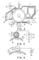
- FIG 3 shows a charging device according to an embodiment of the present invention, wherein reference numeral 1 designates a part of the electrophotographic photosensitive drum which is a member to be charged the photosensitive drum 1 includes a base drum 1a made of aluminum having a photosensitive layer on the outer surface thereof, the photosensitive layer being made of an organic photoconductor (OPC) 1b.
- OPC organic photoconductor
- the outer diameter of the drum 1 is 30 mm, and the drum is rotatable in the direction indicated by an arrow a at a predetermined speed.
- the charging member in the form of a charging roller 2 is contacted to the photosensitive drum 1 a predetermined pressure.
- the charging roller 2 rotates in the direction indicated by an arrow b following the rotation of the photosensitive drum.
- the charging roller 2 may be rotated in the same or opposite direction at the contact area between the photosensitive drum 1 and the charging roller 2, but from the standpoint of the friction between the photosensitive drum 1 and the charging roller 2, it is desirable that the roller 2 is rotated positively or following the photosensitive drum, in the same peripheral direction and at the same speed at the contact area between.
- the charging roller 2 is supplied with a voltage from the voltage source E which applies to the core metal 2a (electrode) of the charging roller 2 a voltage (V DC + V AC ) which is a combination of a DC voltage V DC and an AC voltage V AC .
- the charging roller 2 is of a three layer structure including the core metal, and comprises the metal core 2a (third layer), a conductive elastic layer 2b (second layer) and a resistance or dielectric surface layer (first layer) 2c thereon.
- the outer diameter thereof is 12 mm.
- the dielectric layer is a layer with which an electrostatic capacity of the charging member can be measured by an electrostatic capacity meter.
- the materials of the conductive elastic layer 2b and the surface layer 2c are conductive rubber such as EPDM and regenerated cellulose having a thickness of 10 microns, in this embodiment.
- the resistance of the conductive elastic layer 2b is negligibly small as compared with that of the surface layer 2c, more particularly, it is not more than 103 ohm.
- the resistance R of the charging roller 2 is approximately 107 ohm, and the electrostatic capacity E is approximately 1800 pF.
- the above resistance and the electrostatic capacity are based on 1 cm2 of the roller surface.
- the electrostatic capacity Cd of the photosensitive drum 1 per 1 cm2 is approximately 140 pF.
- the charging roller 2 may be of four layer structure including the core metal.
- the charging member is described in the form of a rotatable roller, but it may be a non-rotatable roller, a pad in the form of a blade or the like.
- the charging roller 2 contacted to the photosensitive member 1 is preferably such that the voltage applied to the core metal 2a (electrode) from the external voltage source 3 is applied between the photosensitive member 1 and the surface layer of the charging roller without attenuation by the resistance of the first layer 2c and the second layer 2b.
- the voltage applied to the core metal 2a (electrode) from the external voltage source 3 is applied between the photosensitive member 1 and the surface layer of the charging roller without attenuation by the resistance of the first layer 2c and the second layer 2b.
- the surface of the photosensitive member 1 has a flaw or the like, the low resistance of the roller 2 tends to result in voltage drop of the external voltage source by an excessive current, as described hereinbefore.
- the low resistance of the roller 2 is desirable whereas from the standpoint of preventing the voltage drop resulting from the flaw, the high resistance of the roller 2 is desirable.
- the resistance which is desirably low because of the charging property is the resistance over the entire contact area between the roller and the photosensitive member
- the resistance which is desirably high because of the prevention of the voltage drop is the resistance between the core metal 2a and the surface flaw of the surface of the photosensitive member.
- the volume resistivity of the outermost resistance layer 2c directly contacted to the photosensitive member (member to be charged) is larger than the volume resistivity of the second layer 2b contacted to the back side of the outermost layer 2c.
- Figure 4 shows a contact type charging device having a core metal 2a and the resistance layer 2b only, as a comparison example.
- the three layer charging roller 2 has a resistance R1 relative to the photosensitive member 1, ⁇ 1: volume resistivity of the first layer 2b ⁇ 2: volume resistivity of the second layer 2c r1: radius of the core metal 2a r2: radius (outer) of the second layer 2b t: thickness of the first layer 2c d: nip width between the charging roller 2 and the photosensitive member 1 l: length of the nip
- the resistance R2 of the charging roller having a single layer 2b as shown in Figure 4, relative to the photosensitive member 1, is,
- FIGS 5A and 1A are longitudinal sectional view of the charging roller of Figures 3 and 4, respectively, wherein the path of the current I through a pin hole P from the charging roller 2 is shown, the pin hole P having been produced by being hit by some member or the like.
- the resistance of the surface layer 2c contacted to the photosensitive member 1 is high, so that the current into the pin hole through the surface layer of the roller is small, and therefore the voltage drop is small.
- the volume resistivity of the surface layer 2c contacted to the member to be charged is larger than the volume resistivity of the layer 2b behind the surface layer, the voltage applied from the external voltage source E is efficiently applied across the contact area between the charging roller and the member to be charged, and in addition, even if the flaw is produced on the surface of the photosensitive member, the excessive current is prevented from flowing, thus preventing the significant voltage drop.
- Figure 6 shows as equivalent circuit of the contact type charging device having the surface layer 2c and the resistance and dielectric layer.
- the resistance R of the charging roller 2 is approximately 107 ohm
- the electrostatic capacity C is approximately 1800 pF.
- the resistance and the electrostatic capacity are on the basis of 1 cm2 of the roller surface.
- the electrostatic capacity Cd of the photosensitive drum 1 per 1 cm2 is approximately 1400 pF.
- the AC voltage V AC which is effective to make uniform the charging of the photosensitive drum 1 can be applied to the photosensitive drum substantially without loss.
- the sign of inequation "»" means sufficiently large difference, and it is preferably different by one order or more. Since the resistance R of the charging roller 2 is sufficiently large, the leakage of current is limited substantially at the pin hole, even if it is produced on the photosensitive drum 1, and therefore, the voltage drop of the voltage source does not occur.
- the impedance component provided by the electrostatic capacity of the roller is smaller than the impedance component provided by the resistance, the leakage can be prevented by the large resistance R, and the AC voltage effective to make the charging uniform can be applied to the photosensitive drum without attenuation by the existence of the capacity C ( Figure 6). Further, since the electrostatic capacity of the roller is larger than the electrostatic capacity of the photosensitive drum, the impedance component of the electrostatic capacity of the roller is smaller than the impedance component of the electrostatic capacity of the drum, the AC voltage can be applied to the photosensitive drum without attenuation.
- FIG 7 there is shown an equivalent circuit of a conventional charging roller 2 shown in Figure 4.
- the resistance R is decreased, the leakage occurs when the photosensitive drum has a pin hole or holes. If the resistance is increased, the leakage can be prevented, but if R ⁇ 1/2 ⁇ fCd, that is, if the impedance component of the resistance of the charging roller is not less than the impedance component of the electrostatic capacity of the drum, the AC voltage V AC is attenuated by the charging roller and is not sufficiently applied to the photosensitive drum, resulting in non-uniform charging.
- the problems are solved, and when an AC voltage V AC having a frequency of 1000 Hz and a peak-to-peal voltage of 1500 Vpp superposed with -750 V DC voltage V DC (substantially the same as the conventional voltages) is applied from the voltage source E, and when the photosensitive drum is rotated at a peripheral speed of 22 mm/sec, the photosensitive drum1 is uniformly charged to -750 V.
- V AC AC voltage
- V DC DC voltage
- the pin hole of the photosensitive drum appears in the image as a black or white spot which is so small that it is not a problem usually.
- the peak-to-peak voltage of the vibratory voltage applied to the charging roller is not less than twice the absolute value of the charge starting voltage when the charging roller is supplied only with a DC voltage, as disclosed in U.S. Serial Nos. 131,585 and 159,917 which have been assigned to the assignee of this application.
- the vibratory voltage is a voltage which periodically change with time, and the waveform may be sine, triangular, rectangular or the like form.
- the charge starting voltage is determined in the following manner.
- the charging roller or member is contacted to a member to be charged having a surface potential of zero, and only a DC voltage is applied to the charging member.
- the DC voltage is increased, and the surface potential of the member to be charged is plotted in a surface potential vs. applied DC voltage graph.
- the voltage is increased with increment of 100 V.
- the first point of the voltage is the one which the surface potential of the member to be charged appears, and ten surface potentials are plotted at each 100 V increment.
- a straight line is drawn from the plots. The DC voltage reading at which the straight line and the line representing the zero surface potential cross is deemed as the charge starting voltage.
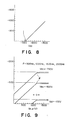
- Figure 8 is a graph illustrating an example of the above method.
- the charge starting voltage was -560 V in this embodiment. If the peak-to-peak voltage is determined so as to be larger than twice the charge starting voltage, the charging can be effected uniformly.
- Figure 9 is a graph of a peak-to-peak voltage of the vibratory voltage applied to the charging roller vs. a surface potential of the OPC photosensitive drum, when the DC voltage is -750, -500, -100 V.
- the peak-to-peak voltage of the vibratory voltage is gradually increased to such an extent that it is not less than twice the absolute value (560 V) of the charge starting voltage, then the surface potential of the photosensitive member becomes uniform.
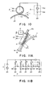
- Figure 10 shows a contact type charging device according to another embodiment of the present invention, wherein the same reference numerals are assigned to the elements having corresponding functions, and the detailed description thereof is omitted.
- the charging roller 2 is of two layer structure having a metal roller 2a and a surface resistance and dielectric layer as a surface layer 2c on the surface of the metal roller 2a.
- the surface layer is of NBR rubber having a thickness of 15 microns.
- the resistance R of the charging roller 2 is approximately 107 ohm, and the electrostatic capacity C is approximately 1500 pF, which satisfy the above-described conditions R > 1/(2 ⁇ fC) and C > Cd, and therefore, the advantages same as those described with the foregoing embodiment can be provided. Since the charging roller 2 does not have the conductive elastic layer in this embodiment, the member to be charged such as the photosensitive drum or the like is preferably has high hardness.
- the charging roller of this embodiment is different from the conventional charging roller as shown in Figure 4 in that the charging roller 2 of this embodiment is provided with a surface resistance and dielectric layer, and therefore, the AC voltage is not attenuated by the charging roller so that the photosensitive member is uniformly charged, and the leakage can be prevented.
- FIG 11 shows a contact type charging device according to a further embodiment.
- the charging member is in the form of a blade codirectisty contacted to the photosensitive drum 1 at a predetermined pressure.
- the blade 12 includes a metal supporting member 12 to which a voltage is supplied and a conductive rubber 12b having a sufficiently low resistance.
- the blade 12 is provided with a surface layer 12c which is a resistance and dielectric layer, where it is contacted to the photosensitive drum 1.
- the surface layer 12c is made of CR rubber having a thickness of 10 microns.
- the resistance R of the charging member is approximately 107 ohm/1 cm2, and the electrostatic capacity C is approximately 1800 pF/1 cm2. Since those values satisfy the above described conditions, the same advantageous effects are provided.
- a metal core (base) 2a having a diameter of 8 mm was coated with the second layer 2b having a thickness of 4 mm and having a resistance of 104 ohm.cm in which carbon was dispersed. It was further coated with the first, that is, surface layer 2c made of cellophane having a thickness of 25 microns and volume resistivity of 109 ohm.cm.
- the charging roller 2 was supplied with a vibratory voltage produced by superposing a DC voltage with an AC voltage having a peak-to-peak voltage which was not less than twice the charge starting voltage to the OPC photosensitive drum, more particularly, the supplied voltage was produced by an AC voltage having a peak-to-peak voltage of 1300 Vpp and a frequency of 1 KHz with a DC voltage of 700 V.
- the OPC photosensitive drum was charged to approximately 700 V. It was confirmed that even if an OPC photosensitive drum which had a pin hole having a diameter of approximately 1 mm, the voltage drop does not occur, and the insufficient charging in the form of a stripe did not occur.
- a metal core (conductive base) 2a having a diameter of 6 mm was coated with cylindrical nitrile butyl rubber having a thickness of 3 mm and having a volume resistivity of 103 ohm.cm in which carbon was dispersed. It was further coated with the first layer 2c of nylon having a thickness of 50 microns and the volume resistivity of 1010 ohm.cm.
- the charging roller 2 thus produced was contacted to the OPC photosensitive drum.
- the charging roller 2 was supplied with a superposed AC and DC voltage (1300 Vpp, 1 KHz AC and 700 V DC).
- the OPC photosensitive drum was driven at a peripheral speed of 22 mm/sec.
- the surface of the OPC photosensitive drum was charged up to approximately 700 V.
- a pin hole having a diameter of approximately 1 mm was formed, and the charging operation was performed. It was confirmed that the voltage drop did not occur, and the uniform charging was provided.
- a charging blade 12 was produced.
- the conductive member 12b (second layer) was produced by dispersing carbon in chloroprene rubber, and the charging blade 12 had a resistivity of 102 ohm.cm, a rubber hardness of 60 degrees and a thickness ta of 1 mm.
- That surface of the conductive member 12b faced to the photosensitive member 1 was coated with the first layer 12c having a thickness of tb.
- usable materials are nylon such as AMILAN (trade name) available from Toray Kabushiki Kaisha, Japan and TORESIN (trade name), available from Teikoku Kagaku Sangyo Kabushiki Kaisha, Japan, material in which the above is dispersed in proper contents, polyurethane rubber, polyurethane elastomer, NBR, chloroprene rubber, PVdF, PVdCl, PFT or the like.
- the thickness tb of the resistance layer 12c of such material was 50 microns.
- An end surface of the conductive member 12b is coated with a material of the resistance layer in the thickness of 200 microns (a). The coating was produced beforehand in a larger thickness, and it was cut accurately with the precision of several microns.
- the charging blade 12 was inclined at an angle ⁇ relative to the photosensitive member 1. More particularly, the angle between a tangent plane and the downstream side of the photosensitive member with respect to movement direction of the photosensitive member was 15 degrees, and the contact width h was about 1 - 2 mm.
- the charging blade 12 was contacted to the surface of the photosensitive drum 1 having an aluminum drum coated with an organic photoconductive material, which was rotated at a peripheral speed of 50 mm/sec.
- the metal supporting member 12a of the charging blade 12 is supplied with a voltage provided by superposing a DC voltage V DC of -700 V and an AC voltage V AC having a peak-to-peak voltage Vpp of 1400 V to charge the surface of the photosensitive member, and the charging and leakage properties were investigated.
- the charging property is evaluated in the following manner.
- the charging blade 12 contacted to the photosensitive member1 is supplied with the voltage provided by superimposing a DC voltage V DC and an AC voltage V AC having a peak-to-peak voltage Vpp which is not less than twice the charge starting voltage relative to the photosensitive member, the photosensitive member is charged, as shown in Figure 9, to a potential which is substantially equal to the DC voltage V DC . Therefore, the charging property is deemed as being good, when the surface potential of the photosensitive member is approximately equal to V DC .
- the leakage property is deemed good when no-charge portion does not appear.
- Figure 12 shows the results. As will be understood from this Figure, when the film thickness tb of the resistance layer 12c of the charging blade 12 is 50 microns, the charging property and the leakage property which are contradictory, are satisfactory when the resistance is 108 - 1012 ohm.cm.
- the volume resistivity is determined by measuring the resistance of 1 cm2 resistance layer 12c with applied voltage of 10 - 1000 V and calculating on the basis thereof since, the values of the respective material of the resistance layer are sometimes slightly different from those given in encyclopedia or catalogue or the like.
- the material of the resistance layer 12c provided good results are AMILAN, TORESIN and a mixture of AMILAN and TORESIN and polyurethane elastomer or NBR having a decreased resistance by dispersing conductive particles.
- An end surface of the conductive member 12b of the charging blade 12 is preferably coated with the resistance layer, since then dust or foreign matter in the air or on the portion of the photosensitive drum surface whicih is not sufficiently cleaned are prevented by the contact of the blade 12 with the rotating photosensitive member 1 from reaching the downstream charging area with respect to the rotational direction of the photosensitive member, and therefore, a partial insufficient charging is avoided.
- spark discharge S due to the leakage current takes place at a position of pin hole P1 resulting in insufficient charge, although the spark discharge does not take place at a position P2.
- the spark discharge result in production of insufficient charge portion.
- the charging blade 2 as shown in Figure 11A, is coated with the resistance layer 12c and a at the surface of the conductive member 12b facing the photosensitive member 1 and at the edge thereof, so that the spark discharge does not occur.
- AMILAN was used as the resistance layer 12c and the layer thickness tb is changed within the range of 5 - 200 microns, and the similar experiments were performed as in the third example to investigate the charging and leakage properties.
- the charging property was good (OK), but the leakage property was no good (NG) if the layer thickness tb is not more than 10 microns. It was found that this was because a pin hole was produced due to dielectric brake down of AMILAN so that the spark discharge occurred when it is contacted to the pin hole, resulting in leakage of the current. Therefore, it was confirmed that a film thickness is required.
- the thickness was preferably not less than 20 microns to be safe with respect to the leakage even if it is damaged.
- Example 3 a charging blade 12 which did not exhibit the leakage was used, and a conductive paint (105 ohm.cm) was painted on the resistance layer 12c. It was confirmed that the leakage took place.
- the lower limit of the resistance preventing the leakage was confirmed as being 108 ohm.cm by Example 3.
- AMILAN having a thickness of 200 microns was used as a resistance layer 2c and the angle ⁇ between the charging blade 12 and the photosensitive member 1 was changed, and similar experiments were performed.
- the angle ⁇ was changed within the range of 5 degrees - 60 degrees. It was confirmed that, the charging property was no good when the angle was larger than 40 degrees.
- the charging blade 12 had the resistivity of 102 ohm.cm and included a conductive urethan rubber blade having a thickness of 1 mm as the conductive member 12b and a resistance layer 12c made of TORESIN or AMILAN having a thickness of 50 microns and having a resistivity of 109 - 1011 ohm.cm at both surfaces and edges.
- the applied voltage was provided by superposing a DC voltage of -700 V and an AC voltage of 1400 Vpp and 500 Hz.
- the resultant surface potential of the photosensitive member was substantially -700 V.
- the charging blade 12 of this Example had a chloroprene sheet having a thickness of 1.5 mm and a resistivity of 102 ohm.cm as the conductive member 12b, and a polyurethane elastomer having a thickness of 50 microns and the resistivity of 1010 ohm.cm was applied on the sheet as a resistance layer 12c.
- the two layer material (12b and 12c) was cut into a proper size and shape and was used as the charging blade.
- the cut edge was coated with a coating layer a made of a polyurethane elastomer having a thickness of 100 microns and a resistivity of 1015 ohm.cm, since otherwise the conductive member 12b is exposed.
- the polyurethane elastomer having the volume resistivity of 1015 ohm.cm used as the coating layer a at the edge of the conductive member had a hardness of 65 degrees, and was used usually as a cleaning blade, so that the property of close contact and the sliding relative to the photosensitive member was very good.
- the angle ⁇ was 10 degrees, and the free portion length was 10 mm, and therefore, the line pressure relative to the photosensitive member is not more than 5 g/cm. Therefore, the photosensitive member is not damaged with good charging property. There is no problem about the leakage property.
- the charging blade 12 comprised a conductive EPTM sheet material having a thickness of 1 mm and the hardness of 70 degrees and having a resistivity of 102 ohm.cm as the conductive member 12b. It was dipped in liquid of TORESIN, AMILAN, NBR or the like, and then it is dried to form the resistance layer 2c. The thickness of the resistance layer 12c was 70 microns at maximum. The resistance layer 12c was applied in the region from an edge faced to the photosensitive member to 4 mm therefrom, and the remainder was not coated. The free portion length l was 8 mm.
- the photosensitive member 1 was contact-charged using discharging blade 12, and it was confirmed that the charging property was good.
- the leakage property since the resistance layer 12c was not formed over the entire surface of the side of the conductive member 12b faced to the photosensitive member 1, but the distance between the conductive member 12b and the pin hole of the photosensitive member was sufficient, and therefore, the spark discharge did not occur.
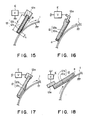
- the charging blade 12 had the same structure as with Figure 11A. However, the charging blade 12 was codirectionally contacted to the photosensitive member 1 although in Figure 11A, it was contacted counter-directionally.
- the surface of the charging blade is gradually spaced apart from the photosensitive member toward downstream of the photosensitive member with respect to the rotational direction thereof, since then the charging is uniform.
- the problem is not significant even if the blade 12 is contacted codirectionally.
- the charging blade 12 counter-directionally contacted to the photosensitive member 1 shown in Figures 15 - 17, may be contacted codirectionally.
- the charging blade 12 in this Example comprises polyurethane elastomer having a thickness of 1 mm and a resistivity of 102 ohm.cm as the conductive member 12b. The end surface thereof is cut into a round surface d.
- the resistance layer 12c is made of a polyurethane elastomer sheet having a thickness of 100 microns and the resistivity of 1010 ohm.cm. It was fused by heat on that surface of the conductive member 12b which is faced to the photosensitive member 1 without air therebetween. The formation of the round surface is effective to decrease the ridigity of the charging blade, and therefore, even if the free portion length l is as small as 5 mm, the pressure to the photosensitive member 1 is not large.
- the ridigity of the end portion of the blade can be decreased, so that the photosensitive member is protected from damage by the charging member 12.
- the surface layer of the charging member is preferably made of resin having a parting property relative to the image bearing member, since then it can be avoided that the softening agent contained in the rubber oozes out and is deposited on the image bearing member to form a film of a toner on the image bearing member and that the flow of the image is produced.
- the nylon resin having a parting property in the foregoing Examples is formed as the surface layer of the charging member with good advantages.
- the high resistance layer is a layer having a resistance which is sufficiently larger than the resistance of the layer behind itself, so that the resistance is negligibly small as compared with the high resistance layer.
- the high resistance layer is defined here as a layer having a resistance not less than 103 times the resistance of the layer therebehind. In this case, the resistance of the charging member is deemed as the same as the resistance of the high resistance layer. Then, the following results: ⁇ l > (E2/P)A
- the thickness of the high resistance layer at a contact area between the charging member and the member to be charged is 3.0 mm, for example, the following results: ⁇ > 2.81 x 101 ohm.m (8)
- the resistance is preferably high. It has been found through experiments by the applicants that the resistance of the charging roller at the nip between the charging roller and the photosensitive drum is preferably approximately 1.14 x 10¹⁰ ohm in consideration of the reduction of the resistance by moisture absorption by the charging roller under a high humidity condition.
- a charging roller 2 having a three layer structure as shown in Figure 3 was used.
- the inside layer 2b of the charging roller 2 was made of a material having the volume resistivity of 101 ohm.m, and the material of the outer layer 2c (the high resistance layer) was selected so that the resistance at the nip portion (sum of the inside layer and the outside layer) is substantially equal to the resistance (1.14x10¹⁰ ohm) of the single layer.
- the outer layer 2c has a larger volume resistivity, and simultaneously, it also acquires an electrostatic capacity.
- the AC current through the charging roller was 0.6 mA in experiments. And, the non-uniformness of the charging of the photosensitive drum was eliminated. It is considered that this is because, in the model of Figure 6, the charging roller has the dielectric layer and also has an electrostatic capacity, so that even if the resistance R is large, the AC current flows through the capacitance C. To do this, as described hereinbefore the impedance (1/2 ⁇ fC) of the capacitance C is preferably smaller than the resistance R. Also, it is effective that the electrostatic capacity of the charging member is larger than that of the member to be charged.
- the high resistance layer in the contact area between the charging member and the photosensitive drum is not limited to the case where the layer 2c includes a single layer as shown in Figure 3, but it may be of a multi-layer structure.
- the layer 2c includes a single layer as shown in Figure 3, but it may be of a multi-layer structure.
- it includes a layer of nylon or AMILAN or the like contactable to the drum and a layer of LBR or other rubber behind it.
- the resistance and the electrostatic capacity of the charging roller at the nip is preferably more limited.
- the material of the outside layer 2c of the charging roller was further investigated. Depending on the material, the surface potential of the charging roller decreases gradually with the rotation of the roller, and finally, the photosensitive drum can not be charged to the predetermined voltage.
- the change in the surface potential of the charging roller 2 is obtained to determine the proper range of the resistance and the electrostatic capacity of the outer layer 2c of the charging roller 2, in the following manner.
- the voltage change through one full turn of the charging roller was obtained using the equivalent circuit.
- the surface potential of the charging roller with which the photosensitive drum can be charged is empilically determined. Thereafter, the resistance and the electrostatic capacity ranges of the outside layer 2c of the charging roller satisfying the above are determined.
- Figure 20 shows an equivalent circuit constituted by the charging roller 2 and the photosensitive drum 1 in the charging roller 2 shown in Figure 3.
- the resistance of the photosensitive drum and the charge starting voltage of the photosensitive drum to the charging roller are taken into account.
- C1, R2 are electrostatic capacity and resistance of the photosensitive drum 1 at the nip portion; C2, R2 are electrostatic capacity and the resistance of the charging roller 2 at the nip; R3 is a charging resistance; E1 is the applied voltage; and E2 is a potential difference between the charging roller surface and the drum surface when the charging of the photosensitive drum starts when the DC voltage to the charging roller is gradually increased, the photosensitive drum having the surface potential of 0 V. This is the instance when the discharge from the roller to the drum starts, and the current at this time is nearly equal to zero, and therefore, the voltage drop by the roller itself is not produced. Thus, E2 can be deemed as the charge starting voltage described above.
- V1, V2 are voltages applied to the photosensitive drum 1 and to the charging roller 2;
- S is a switch which is closed when a particular portion of the periphery of the charging roller comes to the nip, and is opened when it departs from the nip.
- Figure 21 shows the change in the surface potential of the charging roller resulting from the equivalent circuit of Figure 20 (E1-V2).
- t1 is the time required for the charging roller passes through the nip
- t2 is the time required for the charging roller rotates through one full turn.
- the time is t1 when the particular portion departs from the nip, and the discharge ends. During this period, the switch Sw is considered to be closed.
- the discharge starts at the nip portion after the charging roller 2 rotates through one turn at the time t2.
- the charging roller 2 is away from the nip so that the discharge does not occur, the switch Sw is opened.
- the electric charge q2 in the capacitance C2 attenuates by discharge through the resistance R2. This means that the charging roller 2 having been electrically charged is electrically discharged by the leakage of the current, that is, the residual charge is removed.
- the electric discharge occurs where the charging roller and the photosensitive drum is spaced apart with a small clearance, and therefore, the charging area has a width which is slightly large than the nip formed between the charging roller and the photosensitive drum.
- a small clearance region is sufficiently negligibly small as compared with the nip width, and therefore, the charging area is considered as being equal to the nip.
- V 2(o) initial voltage of the charging roller which is a voltage of the charging roller when the previous charge is retained before the rotation of the charging roller starts.
- the voltage of the charging roller at the nip is:
- the voltage of the charging roller when the portion considered is again introduced into the nip after it is once departed from the nip, is:
- the surface potential of the charging roller at the time when the portion considered is departed from the nip is indicated by a chain line in Figure 21.
- (9) - (12) designate the parts represented by the above equations (9) - (12).
- the chain lines with two dots indicate the change in the surface potential of the photosensitive drum. This is always lower than the surface potential (E1-V2) of the charging roller by E2.
- the photosensitive drum When the saturated surface potential of the charging roller is to be measured in experiments, the photosensitive drum is continuously charged, and the potential thereof at the position where a portion considered departs the nip, and the measurements are plotted on a graph of potential vs. time. The potential gradually reaches the final potential, and asymptotic line is determined as the saturated potential.
- the range is provided from the above equation (12) as follows.
- the applied voltage E1 -1300 V
- the resistance R1 of the photosensitive drum at the nip is 4.00x10¹² ohm
- the electrostatic capacity C1 3.10x10 ⁇ 10 F.
- the photosensitive member was an OPC photosensitive member. The voltage is dependent on the polarity of the applied voltage and the electrostatic capacity of the photosensitive member.
- the voltage (E1-V2) is larger than the voltage E2 if the following is satisfied:
- the resistance R2 of the nip portion when the outside layer 2c has the volume resistivity satisfying the above considering that the resistance of the layer behind the high resistance layer is sufficiently smaller than that of the high resistance layer, and therefore, it is negligible small, is obtained as follows.:
- the range of the resistance R2 is as follows:
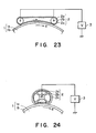
- the charging member has been in the form of a roller, but as shown in Figure 23, the outside layer 2c (the high resistance layer) of the charging roller 2 is in the form of a belt.
- the time for the residual charge in the outside layer 2c to dissipate is made longer, so that the recovery of the charging power is promoted.
- the resistance of the material of the outside layer 2c is allowed to be further larger, thus providing a wider latitude of material selection.
- the charging width is made larger to ensure the charging.
- the inside layer 2b of the charging roller may be a hollow honeycomb shape or sponge-like shape. In this case, it is possible to easy obtain a relatively wide nip width, and therefore, the advantages provided by the belt form can be provided.
- the pin hole having an area of 1 mm2 as an example, but in the case of high quality image formation, the pin hole having the area of 0.001 mm2 (0.1 mm x 0.1 mm) is to be considered.
- the inequation (6) is expressed as follows: ⁇ l > E2x(0.1x10 ⁇ 3)2/P (ohm.m2)
- the photosensitive member is not limited to the OPC photosensitive member, and the photosensitive member made of amorphous silicon or selenium or the like can be used.
- the photosensitive member is not limited to the form of drum but may be in the form of a belt or sheet.
- the member to be charged is not limited to the photosensitive member, and an insulating drum not having the photosensitive layer can be used.
- the present invention in the charging device wherein the charging means supplied with the voltage is contacted to the member to be charged to perform the charging, the leakage current from the charging means to the member to be charged is prevented, and therefore, the no-charge portion of the member is not produced.
- the member to be charged is charged uniformly. Further, when the charging means is repeatedly operated, the charging power of the charging means can be maintained.
Landscapes
- Physics & Mathematics (AREA)
- Engineering & Computer Science (AREA)
- Plasma & Fusion (AREA)
- General Physics & Mathematics (AREA)
- Electrostatic Charge, Transfer And Separation In Electrography (AREA)
Applications Claiming Priority (10)
| Application Number | Priority Date | Filing Date | Title |
|---|---|---|---|
| JP230334/87 | 1987-09-14 | ||
| JP230333/87 | 1987-09-14 | ||
| JP23033487A JPS6473364A (en) | 1987-09-14 | 1987-09-14 | Contact electrifying device |
| JP23033387A JPS6473367A (en) | 1987-09-14 | 1987-09-14 | Contact electrostatic charging device |
| JP251294/87 | 1987-10-05 | ||
| JP62251294A JP2505822B2 (ja) | 1987-10-05 | 1987-10-05 | 帯電装置 |
| JP62331149A JPH0792617B2 (ja) | 1987-12-26 | 1987-12-26 | 接触帯電装置 |
| JP331149/87 | 1987-12-26 | ||
| JP331150/87 | 1987-12-26 | ||
| JP33115087A JPH01172858A (ja) | 1987-12-26 | 1987-12-26 | 接触帯電装置 |
Publications (3)
| Publication Number | Publication Date |
|---|---|
| EP0308185A2 true EP0308185A2 (de) | 1989-03-22 |
| EP0308185A3 EP0308185A3 (en) | 1989-08-23 |
| EP0308185B1 EP0308185B1 (de) | 1993-11-24 |
Family
ID=27529855
Family Applications (1)
| Application Number | Title | Priority Date | Filing Date |
|---|---|---|---|
| EP88308464A Expired - Lifetime EP0308185B1 (de) | 1987-09-14 | 1988-09-13 | Aufladevorrichtung |
Country Status (3)
| Country | Link |
|---|---|
| US (1) | US5126913A (de) |
| EP (1) | EP0308185B1 (de) |
| DE (1) | DE3885830T2 (de) |
Cited By (32)
| Publication number | Priority date | Publication date | Assignee | Title |
|---|---|---|---|---|
| EP0328113A2 (de) * | 1988-02-11 | 1989-08-16 | Canon Kabushiki Kaisha | Bauteil zum Aufladen |
| FR2651901A1 (fr) * | 1989-09-14 | 1991-03-15 | Canon Kk | Appareil de formation d'images. |
| EP0439168A2 (de) * | 1990-01-24 | 1991-07-31 | Canon Kabushiki Kaisha | Aufladegerät |
| EP0439143A2 (de) * | 1990-01-24 | 1991-07-31 | Canon Kabushiki Kaisha | Auflade-Element mit einer Schnittkante, und dieses Element verwendende Aufladevorrichtung in einer abnehmbaren Arbeitseinheit für ein Bilderzeugungsgerät |
| EP0439145A2 (de) * | 1990-01-24 | 1991-07-31 | Canon Kabushiki Kaisha | Auflade-Element mit einer Elektrodenstruktur und dieses verwendende Aufladevorrichtung in einer abnehmbaren Arbeitseinheit für ein Bilderzeugungsgerät |
| EP0443800A2 (de) * | 1990-02-17 | 1991-08-28 | Canon Kabushiki Kaisha | Aufladeverfahren und Aufladevorrichtung |
| EP0458273A2 (de) * | 1990-05-21 | 1991-11-27 | Canon Kabushiki Kaisha | Aufladevorrichtung, BilderzeugungsgerÀ¤t mit einer solchen Vorrichtung und von dem Bilderzeugungsgerät abnehmbare Arbeitseinheit |
| EP0496399A2 (de) * | 1991-01-24 | 1992-07-29 | Canon Kabushiki Kaisha | Aufladevorrichtung zum Aufladen eines sich in der Nähe befindendes Elementes und Bilderzeugungsgerät mit einer solchen Vorrichtung |
| US5144368A (en) * | 1989-11-15 | 1992-09-01 | Canon Kabushiki Kaisha | Charging device and image forming apparatus having same |
| EP0504877A2 (de) * | 1991-03-20 | 1992-09-23 | Canon Kabushiki Kaisha | Aufladeelement, Aufladevorrichtung, Arbeitseinheit und Bilderzeugungsgerät mit einem Aufladeelement |
| US5192974A (en) * | 1991-02-06 | 1993-03-09 | Minolta Camera Kabushiki Kaisha | Contract charger |
| DE4240549A1 (en) * | 1991-12-02 | 1993-06-03 | Ricoh Kk | Electrostatic copier or printer with DC energised charging roller - has composite roller with metal core and flexible layers in contact with photosensitive drum for reduced cost and ozone emission. |
| US5217836A (en) * | 1989-11-09 | 1993-06-08 | Canon Kabushiki Kaisha | Toner for developing electrostatic images |
| EP0562857A2 (de) * | 1992-03-26 | 1993-09-29 | Mita Industrial Co. Ltd. | Elektrifizierungsverfahren und dafür verwendetes Gerät |
| EP0574208A2 (de) * | 1992-06-08 | 1993-12-15 | Canon Kabushiki Kaisha | Aufladungsteil und Bilderzeugungsgerät mit einem Kontaktaufladungsteil |
| US5278614A (en) * | 1992-05-15 | 1994-01-11 | Minolta Camera Kabushiki Kaisha | Contact charger and image forming apparatus incorporating the contact charger |
| EP0590912A2 (de) * | 1992-09-28 | 1994-04-06 | Mita Industrial Co., Ltd. | Verfahren zum Kontaktaufladen der Oberfläche eines photoempfindlichen Materials |
| EP0593245A1 (de) * | 1992-10-15 | 1994-04-20 | Konica Corporation | Bilderzeugungsgerät mit Magnetbürsten-Bildträgeraufladevorrichtung |
| EP0596477A2 (de) * | 1992-11-04 | 1994-05-11 | Canon Kabushiki Kaisha | Aufladungsteil und Gerät hiermit |
| DE4337876A1 (de) * | 1992-11-06 | 1994-06-09 | Seiko Epson Corp | Kontaktladevorrichtungen und Kontaktübertragungsvorrichtungen |
| US5321472A (en) * | 1990-01-24 | 1994-06-14 | Canon Kabushiki Kaisha | Charging member with a bridging electrode structure and charging device using same in an image forming apparatus |
| US5376485A (en) * | 1989-11-13 | 1994-12-27 | Canon Kabushiki Kaisha | Photosensitive member, electrophotographic apparatus and image forming method using same |
| EP0631205A2 (de) * | 1993-06-24 | 1994-12-28 | Tokai Rubber Industries, Ltd. | Elektrisch leitende Rolle mit einer Basisschicht aus ionen-leitendem Material |
| US5391449A (en) * | 1990-06-04 | 1995-02-21 | Canon Kabushiki Kaisha | Electrophotographic photosensitive member |
| EP0646849A2 (de) * | 1993-09-30 | 1995-04-05 | Mita Industrial Co. Ltd. | Verfahren und Vorrichtung zum elektrischen Aufladen |
| US5420671A (en) * | 1988-04-20 | 1995-05-30 | Canon Kabushiki Kaisha | Charger and image forming apparatus with same |
| EP0678793A2 (de) * | 1994-04-22 | 1995-10-25 | Tokai Rubber Industries, Ltd. | Leitfähige Rolle und Verfahren um die Rolle herzustellen |
| US5475472A (en) * | 1991-10-04 | 1995-12-12 | Canon Kabushiki Kaisha | Image process unit having charging member impedance correction feature |
| US5517289A (en) * | 1991-10-30 | 1996-05-14 | Oki Electric Industry Co., Ltd. | Apparatus for and method of forming image |
| EP0720069A3 (de) * | 1994-12-22 | 1997-02-26 | Canon Kk | Aufladeelement, Arbeitseinheit mit einem solchen Element und elektrophotographisches Gerät |
| US6190295B1 (en) | 1998-02-24 | 2001-02-20 | Tokai Rubber Industries, Ltd. | Charging roll whose resistance adjusting layer contains insulating particles dispersed therein |
| DE10035104B4 (de) * | 1999-07-19 | 2012-06-14 | Ricoh Co., Ltd. | Vorrichtung zur Bilderzeugung, welche zur wirksamen Aufrechterhaltung eines Ladungspotenzials im Stande ist |
Families Citing this family (46)
| Publication number | Priority date | Publication date | Assignee | Title |
|---|---|---|---|---|
| US5307122A (en) * | 1989-07-28 | 1994-04-26 | Canon Kabushiki Kaisha | Image forming apparatus apparatus unit facsimile apparatus and developer comprising hydrophobic silica fine powder for developing electrostatic images |
| JPH04268583A (ja) * | 1991-02-22 | 1992-09-24 | Canon Inc | 帯電装置 |
| JP2962919B2 (ja) * | 1991-03-01 | 1999-10-12 | キヤノン株式会社 | プロセスカートリッジ及び画像形成装置 |
| US5270768A (en) * | 1991-04-24 | 1993-12-14 | Canon Kabushiki Kaisha | Charging member containing reduced titanium oxide and device using same |
| EP0554114B1 (de) * | 1992-01-30 | 1998-09-09 | Canon Kabushiki Kaisha | Aufladungsteil, Aufladungsvorrichtung, Prozesskassette und Bilderzeugungsgerät |
| US5293200A (en) * | 1992-02-18 | 1994-03-08 | Brother Kogyo Kabushiki Kaisha | Electrostatic device for charging a photosensitive surface |
| JPH05265263A (ja) * | 1992-03-18 | 1993-10-15 | Hitachi Metals Ltd | 電子写真プリンタ |
| US5237375A (en) * | 1992-05-13 | 1993-08-17 | Steven Bruce Michlin | Wiper and spreader blade stiffener |
| JP3320102B2 (ja) * | 1992-06-30 | 2002-09-03 | キヤノン株式会社 | プロセスカートリッジ及び画像形成装置 |
| JPH0635302A (ja) * | 1992-07-16 | 1994-02-10 | Canon Inc | 画像形成装置 |
| JP2947019B2 (ja) * | 1992-11-06 | 1999-09-13 | セイコーエプソン株式会社 | 接触型電荷供給装置 |
| DE4345490C2 (de) * | 1992-11-06 | 2000-03-09 | Seiko Epson Corp | Kontaktladevorrichtung |
| US5552865A (en) * | 1993-02-09 | 1996-09-03 | Minolta Camera Kabushiki Kaisha | Charging device and method for charging a charge-receiving member by a charging member by discharge therebetween based on difference in electric potential between the charging member and the charge-receiving member |
| US5471285A (en) * | 1993-04-16 | 1995-11-28 | Bando Chemical Industries, Ltd. | Charging member having a surface layer formed of moisture-permeable synthetic resin material and charging device including the same |
| US5367364A (en) * | 1993-05-19 | 1994-11-22 | Steven B. Michlin | Charge roller contact stabilizer spring |
| TW272259B (de) * | 1993-05-31 | 1996-03-11 | Mitsuta Industry Co Ltd | |
| US5535088A (en) * | 1993-06-17 | 1996-07-09 | Brother Kogyo Kabushiki Kaisha | Contacting charging device for electrostatic photoreceptor drum |
| JPH0728306A (ja) * | 1993-07-07 | 1995-01-31 | Canon Inc | 帯電部材、帯電装置、画像形成装置、及びプロセス カートリッジ |
| JPH0728309A (ja) * | 1993-07-13 | 1995-01-31 | Toshiba Corp | 画像形成装置 |
| EP0843231B1 (de) * | 1993-07-30 | 2001-10-31 | Canon Kabushiki Kaisha | Aufladungsteil, Aufladevorrichtung und aus einem Bilderzeugungsgerät herausnehmbare Prozesskassette |
| EP0642063B1 (de) * | 1993-09-07 | 1999-05-06 | Matsushita Electric Industrial Co., Ltd. | Aufladevorrichtung und Bilderzeugungsgerät mit der Aufladevorrichtung |
| JP3747478B2 (ja) * | 1993-10-27 | 2006-02-22 | コニカミノルタビジネステクノロジーズ株式会社 | 接触帯電装置 |
| DE69425954T2 (de) * | 1993-12-28 | 2001-01-18 | Matsushita Electric Industrial Co., Ltd. | Aufladevorrichtung, Bilderzeugungsgerät mit der Aufladevorrichtung und Verfahren zur Herstellung der Vorrichtung |
| US5576805A (en) * | 1994-03-16 | 1996-11-19 | Canon Kabushiki Kaisha | Contact charging member for charging a photosensitive drum having improved durability and a method for making the same |
| US5506745A (en) * | 1994-08-05 | 1996-04-09 | Xerox Corporation | Hollow conformable charge roll |
| JPH0869152A (ja) * | 1994-08-26 | 1996-03-12 | Minolta Co Ltd | 接触帯電装置 |
| US5475313A (en) * | 1994-09-20 | 1995-12-12 | Dykes; Wallace E. | Primary charge roller evaluator |
| JPH08137206A (ja) * | 1994-11-10 | 1996-05-31 | Minolta Co Ltd | 画像形成装置 |
| US5740008A (en) * | 1995-04-18 | 1998-04-14 | Bridgestone Corporation | Charging member and device |
| US5689776A (en) * | 1995-10-04 | 1997-11-18 | Xerox Corporation | Contact charging system for uniformly charging a charge retentive surface |
| US5581329A (en) * | 1995-10-05 | 1996-12-03 | Imaging Rechargers Inc. | Contact charger |
| KR200153521Y1 (ko) * | 1996-02-17 | 1999-09-01 | 윤종용 | 전자 사진 인쇄장치의 보조 대전 장치 |
| US6434351B2 (en) | 1996-05-30 | 2002-08-13 | Canon Kabushiki Kaisha | Electrophotographic photosensitive member, and process cartridge and electrophotographic apparatus employing the same |
| US6324365B1 (en) | 1996-05-30 | 2001-11-27 | Canon Kabushiki Kaisha | Electrophotographic photosensitive member, and process cartridge and electrophotographic apparatus employing the same |
| KR100204554B1 (ko) * | 1997-02-28 | 1999-06-15 | 백정호 | 대전 롤러의 제조방법 |
| JP2001042597A (ja) | 1999-08-04 | 2001-02-16 | Sharp Corp | 接触帯電装置 |
| JP2002055512A (ja) * | 2000-05-30 | 2002-02-20 | Ricoh Co Ltd | 帯電装置および該帯電装置を有する画像形成装置 |
| WO2004070474A1 (ja) * | 2003-02-07 | 2004-08-19 | Sharp Kabushiki Kaisha | 電子写真感光体およびそれを備える画像形成装置 |
| JP3718508B2 (ja) * | 2003-06-03 | 2005-11-24 | シャープ株式会社 | 電子写真感光体およびそれを備える画像形成装置 |
| KR100555734B1 (ko) * | 2004-02-17 | 2006-03-03 | 삼성전자주식회사 | 화상형성장치 |
| DE102005024380B4 (de) * | 2005-05-27 | 2007-05-16 | Oce Printing Systems Gmbh | Vorrichtung und Verfahren zum elektrischen Aufladen eines Transportbandes unter Verwendung einer Kontaktlippe aus einem Gummimaterial |
| JP5157097B2 (ja) * | 2006-07-18 | 2013-03-06 | 株式会社リコー | 画像形成装置の帯電工程評価方法 |
| JP4544341B2 (ja) * | 2008-04-30 | 2010-09-15 | 富士ゼロックス株式会社 | 帯電装置及びこれを用いた画像形成組立体、画像形成装置 |
| JP5901227B2 (ja) | 2010-12-14 | 2016-04-06 | キヤノン株式会社 | 帯電部材および画像形成装置 |
| JP2012128079A (ja) * | 2010-12-14 | 2012-07-05 | Canon Inc | 帯電部材および画像形成装置 |
| JP5615154B2 (ja) * | 2010-12-14 | 2014-10-29 | キヤノン株式会社 | 帯電部材および画像形成装置 |
Citations (6)
| Publication number | Priority date | Publication date | Assignee | Title |
|---|---|---|---|---|
| US3626260A (en) * | 1968-03-19 | 1971-12-07 | Iwatsu Electric Co Ltd | Method and apparatus for applying voltage in electrophotography |
| US3778690A (en) * | 1972-03-16 | 1973-12-11 | Copy Res Corp | Electrostatic copying machine |
| EP0035745A2 (de) * | 1980-03-10 | 1981-09-16 | Kabushiki Kaisha Toshiba | Aufladevorrichtung |
| DE3101678A1 (de) * | 1980-01-25 | 1981-12-17 | Tokyo Shibaura Denki K.K., Kawasaki, Kanagawa | Elektronisches bzw. elektrophotographisches kopiergeraet |
| JPS5772157A (en) * | 1980-10-22 | 1982-05-06 | Toshiba Corp | Electrostatic charger |
| EP0272072A2 (de) * | 1986-12-15 | 1988-06-22 | Canon Kabushiki Kaisha | Aufladevorrichtung |
Family Cites Families (2)
| Publication number | Priority date | Publication date | Assignee | Title |
|---|---|---|---|---|
| US2980834A (en) * | 1956-04-26 | 1961-04-18 | Bruning Charles Co Inc | Charging of photo-conductive insulating material |
| US2934649A (en) * | 1957-01-09 | 1960-04-26 | Haloid Xerox Inc | Induction charging |
-
1988
- 1988-09-13 DE DE3885830T patent/DE3885830T2/de not_active Expired - Lifetime
- 1988-09-13 EP EP88308464A patent/EP0308185B1/de not_active Expired - Lifetime
-
1991
- 1991-08-29 US US07/753,027 patent/US5126913A/en not_active Expired - Lifetime
Patent Citations (6)
| Publication number | Priority date | Publication date | Assignee | Title |
|---|---|---|---|---|
| US3626260A (en) * | 1968-03-19 | 1971-12-07 | Iwatsu Electric Co Ltd | Method and apparatus for applying voltage in electrophotography |
| US3778690A (en) * | 1972-03-16 | 1973-12-11 | Copy Res Corp | Electrostatic copying machine |
| DE3101678A1 (de) * | 1980-01-25 | 1981-12-17 | Tokyo Shibaura Denki K.K., Kawasaki, Kanagawa | Elektronisches bzw. elektrophotographisches kopiergeraet |
| EP0035745A2 (de) * | 1980-03-10 | 1981-09-16 | Kabushiki Kaisha Toshiba | Aufladevorrichtung |
| JPS5772157A (en) * | 1980-10-22 | 1982-05-06 | Toshiba Corp | Electrostatic charger |
| EP0272072A2 (de) * | 1986-12-15 | 1988-06-22 | Canon Kabushiki Kaisha | Aufladevorrichtung |
Non-Patent Citations (1)
| Title |
|---|
| PATENT ABSTRACTS OF JAPAN, vol. 6, no. 156 (P-135)[1034], 17th August 1982; & JP-A-57 72 157 (TOKYO SHIBAURA DENKI K.K.) 06-05-1982 * |
Cited By (68)
| Publication number | Priority date | Publication date | Assignee | Title |
|---|---|---|---|---|
| EP0328113A3 (en) * | 1988-02-11 | 1990-08-01 | Canon Kabushiki Kaisha | Member for charging |
| EP0328113A2 (de) * | 1988-02-11 | 1989-08-16 | Canon Kabushiki Kaisha | Bauteil zum Aufladen |
| US5112708A (en) * | 1988-02-11 | 1992-05-12 | Canon Kabushiki Kaisha | Member for charging with surface layer of n-alkoxymethylated nylon effecting charging at lower voltage |
| US5420671A (en) * | 1988-04-20 | 1995-05-30 | Canon Kabushiki Kaisha | Charger and image forming apparatus with same |
| EP0417801A3 (en) * | 1989-09-14 | 1992-08-26 | Canon Kabushiki Kaisha | Image forming apparatus having charging means |
| FR2651901A1 (fr) * | 1989-09-14 | 1991-03-15 | Canon Kk | Appareil de formation d'images. |
| EP0417801A2 (de) * | 1989-09-14 | 1991-03-20 | Canon Kabushiki Kaisha | Bilderzeugungsgerät mit Aufladungsmitteln |
| US5217836A (en) * | 1989-11-09 | 1993-06-08 | Canon Kabushiki Kaisha | Toner for developing electrostatic images |
| CN1037998C (zh) * | 1989-11-13 | 1998-04-08 | 佳能公司 | 光敏元件和光电成象设备以及用其成象的方法 |
| US5376485A (en) * | 1989-11-13 | 1994-12-27 | Canon Kabushiki Kaisha | Photosensitive member, electrophotographic apparatus and image forming method using same |
| US5144368A (en) * | 1989-11-15 | 1992-09-01 | Canon Kabushiki Kaisha | Charging device and image forming apparatus having same |
| US5353101A (en) * | 1990-01-24 | 1994-10-04 | Canon Kabushiki Kaisha | Charging member featuring a cut edge, and charging device employing same for use in a detachable process unit in an image forming apparatus |
| EP0439168A2 (de) * | 1990-01-24 | 1991-07-31 | Canon Kabushiki Kaisha | Aufladegerät |
| EP0439143A3 (en) * | 1990-01-24 | 1992-12-09 | Canon Kabushiki Kaisha | Charging member featureing a cut edge, and charging device employing same for use in a detachable process unit in an image forming apparatus |
| EP0439145A3 (en) * | 1990-01-24 | 1992-12-09 | Canon Kabushiki Kaisha | Charging member with a bridging electrode structure and charging device using same in a detachable process unit in an image forming apparatus |
| EP0439143A2 (de) * | 1990-01-24 | 1991-07-31 | Canon Kabushiki Kaisha | Auflade-Element mit einer Schnittkante, und dieses Element verwendende Aufladevorrichtung in einer abnehmbaren Arbeitseinheit für ein Bilderzeugungsgerät |
| EP0439168A3 (en) * | 1990-01-24 | 1993-01-20 | Canon Kabushiki Kaisha | A charger |
| EP0439145A2 (de) * | 1990-01-24 | 1991-07-31 | Canon Kabushiki Kaisha | Auflade-Element mit einer Elektrodenstruktur und dieses verwendende Aufladevorrichtung in einer abnehmbaren Arbeitseinheit für ein Bilderzeugungsgerät |
| US5357322A (en) * | 1990-01-24 | 1994-10-18 | Canon Kabushiki Kaisha | Charger |
| US5321472A (en) * | 1990-01-24 | 1994-06-14 | Canon Kabushiki Kaisha | Charging member with a bridging electrode structure and charging device using same in an image forming apparatus |
| EP0443800A2 (de) * | 1990-02-17 | 1991-08-28 | Canon Kabushiki Kaisha | Aufladeverfahren und Aufladevorrichtung |
| EP0443800A3 (en) * | 1990-02-17 | 1992-05-13 | Canon Kabushiki Kaisha | A charging device |
| US5146280A (en) * | 1990-02-17 | 1992-09-08 | Canon Kabushiki Kaisha | Charging device |
| US5459558A (en) * | 1990-05-21 | 1995-10-17 | Canon Kabushiki Kaisha | Charging device, image forming apparatus with same and a process unit detachably mountable to the image forming apparatus |
| EP0458273A2 (de) * | 1990-05-21 | 1991-11-27 | Canon Kabushiki Kaisha | Aufladevorrichtung, BilderzeugungsgerÀ¤t mit einer solchen Vorrichtung und von dem Bilderzeugungsgerät abnehmbare Arbeitseinheit |
| EP0458273A3 (en) * | 1990-05-21 | 1993-01-13 | Canon Kabushiki Kaisha | Charging device, image forming apparatus with same and a process unit detachable mountable to the image forming apparatus |
| EP0460558B1 (de) * | 1990-06-04 | 1996-02-07 | Canon Kabushiki Kaisha | Lichtempfindliches Element zur Elektrophotographie |
| US5391449A (en) * | 1990-06-04 | 1995-02-21 | Canon Kabushiki Kaisha | Electrophotographic photosensitive member |
| EP0496399A2 (de) * | 1991-01-24 | 1992-07-29 | Canon Kabushiki Kaisha | Aufladevorrichtung zum Aufladen eines sich in der Nähe befindendes Elementes und Bilderzeugungsgerät mit einer solchen Vorrichtung |
| EP0496399A3 (en) * | 1991-01-24 | 1993-07-07 | Canon Kabushiki Kaisha | Charging device disposed close to member to be charged and image forming apparatus using same |
| US5192974A (en) * | 1991-02-06 | 1993-03-09 | Minolta Camera Kabushiki Kaisha | Contract charger |
| EP0504877A2 (de) * | 1991-03-20 | 1992-09-23 | Canon Kabushiki Kaisha | Aufladeelement, Aufladevorrichtung, Arbeitseinheit und Bilderzeugungsgerät mit einem Aufladeelement |
| US5541711A (en) * | 1991-03-20 | 1996-07-30 | Canon Kabushiki Kaisha | Charging member having a cavity, charging device, process unit, and image forming apparatus having such a charging member |
| EP0504877A3 (en) * | 1991-03-20 | 1993-07-07 | Canon Kabushiki Kaisha | Charging member, charging device, process unit and image forming apparatus having charging member |
| US5475472A (en) * | 1991-10-04 | 1995-12-12 | Canon Kabushiki Kaisha | Image process unit having charging member impedance correction feature |
| US5517289A (en) * | 1991-10-30 | 1996-05-14 | Oki Electric Industry Co., Ltd. | Apparatus for and method of forming image |
| DE4240549A1 (en) * | 1991-12-02 | 1993-06-03 | Ricoh Kk | Electrostatic copier or printer with DC energised charging roller - has composite roller with metal core and flexible layers in contact with photosensitive drum for reduced cost and ozone emission. |
| DE4240549C2 (de) * | 1991-12-02 | 1998-01-29 | Ricoh Kk | Ladevorrichtung mit einer drehbaren Laderolle zum Laden eines photoleitfähigen Elements |
| US5881344A (en) * | 1991-12-02 | 1999-03-09 | Ricoh Company, Ltd. | Image forming apparatus and charging device thereof |
| EP0562857A2 (de) * | 1992-03-26 | 1993-09-29 | Mita Industrial Co. Ltd. | Elektrifizierungsverfahren und dafür verwendetes Gerät |
| EP0562857A3 (de) * | 1992-03-26 | 1994-03-16 | Mita Industrial Co Ltd | |
| US5446615A (en) * | 1992-03-26 | 1995-08-29 | Mita Industrial Co., Ltd. | Electrifying method and electrifying apparatus used therefor |
| US5278614A (en) * | 1992-05-15 | 1994-01-11 | Minolta Camera Kabushiki Kaisha | Contact charger and image forming apparatus incorporating the contact charger |
| EP0574208A2 (de) * | 1992-06-08 | 1993-12-15 | Canon Kabushiki Kaisha | Aufladungsteil und Bilderzeugungsgerät mit einem Kontaktaufladungsteil |
| EP0574208A3 (de) * | 1992-06-08 | 1994-02-02 | Canon Kabushiki Kaisha | Aufladungsteil und Bilderzeugungsgerät mit einem Kontaktaufladungsteil |
| US5671468A (en) * | 1992-06-08 | 1997-09-23 | Canon Kabushiki Kaisha | Charging member and image forming apparatus having contact charging member |
| US5485344A (en) * | 1992-09-28 | 1996-01-16 | Mita Industrial Co., Ltd. | Method of contact-charging the surface of a photosensitive material |
| EP0590912A2 (de) * | 1992-09-28 | 1994-04-06 | Mita Industrial Co., Ltd. | Verfahren zum Kontaktaufladen der Oberfläche eines photoempfindlichen Materials |
| EP0590912A3 (de) * | 1992-09-28 | 1995-04-19 | Mita Industrial Co Ltd | Verfahren zum Kontaktaufladen der Oberfläche eines photoempfindlichen Materials. |
| EP0593245A1 (de) * | 1992-10-15 | 1994-04-20 | Konica Corporation | Bilderzeugungsgerät mit Magnetbürsten-Bildträgeraufladevorrichtung |
| US5381215A (en) * | 1992-10-15 | 1995-01-10 | Konica Corporation | Image forming apparatus having charger to charge image carrier with magnetic brush |
| US5502548A (en) * | 1992-11-04 | 1996-03-26 | Canon Kabushiki Kaisha | Contact-type charging member which includes an insulating metal oxide in a surface layer thereof |
| EP0596477A2 (de) * | 1992-11-04 | 1994-05-11 | Canon Kabushiki Kaisha | Aufladungsteil und Gerät hiermit |
| EP0596477A3 (de) * | 1992-11-04 | 1995-03-08 | Canon Kk | Aufladungsteil und Gerät hiermit. |
| DE4337876C2 (de) * | 1992-11-06 | 2000-07-20 | Seiko Epson Corp | Kontaktladungszuführvorrichtung |
| DE4337876A1 (de) * | 1992-11-06 | 1994-06-09 | Seiko Epson Corp | Kontaktladevorrichtungen und Kontaktübertragungsvorrichtungen |
| EP0631205A3 (de) * | 1993-06-24 | 1995-09-06 | Tokai Rubber Ind Ltd | Elektrisch leitende Rolle mit einer Basisschicht aus ionen-leitendem Material. |
| US5604031A (en) * | 1993-06-24 | 1997-02-18 | Tokai Rubber Industries, Ltd. | Electrically conductive roll whose base layer is formed of ion-conductive elastic material |
| EP0631205A2 (de) * | 1993-06-24 | 1994-12-28 | Tokai Rubber Industries, Ltd. | Elektrisch leitende Rolle mit einer Basisschicht aus ionen-leitendem Material |
| US5659853A (en) * | 1993-09-30 | 1997-08-19 | Mita Industrial Co., Ltd. | Electrically charging method and electrically charging device used therefor |
| EP0646849A3 (de) * | 1993-09-30 | 1995-07-26 | Mita Industrial Co Ltd | Verfahren und Vorrichtung zum elektrischen Aufladen. |
| EP0646849A2 (de) * | 1993-09-30 | 1995-04-05 | Mita Industrial Co. Ltd. | Verfahren und Vorrichtung zum elektrischen Aufladen |
| EP0678793A3 (de) * | 1994-04-22 | 1998-05-20 | Tokai Rubber Industries, Ltd. | Leitfähige Rolle und Verfahren um die Rolle herzustellen |
| EP0678793A2 (de) * | 1994-04-22 | 1995-10-25 | Tokai Rubber Industries, Ltd. | Leitfähige Rolle und Verfahren um die Rolle herzustellen |
| US5713067A (en) * | 1994-12-22 | 1998-01-27 | Canon Kabushiki Kaisha | Charging member, process cartridge using the same and electrophotographic apparatus |
| EP0720069A3 (de) * | 1994-12-22 | 1997-02-26 | Canon Kk | Aufladeelement, Arbeitseinheit mit einem solchen Element und elektrophotographisches Gerät |
| US6190295B1 (en) | 1998-02-24 | 2001-02-20 | Tokai Rubber Industries, Ltd. | Charging roll whose resistance adjusting layer contains insulating particles dispersed therein |
| DE10035104B4 (de) * | 1999-07-19 | 2012-06-14 | Ricoh Co., Ltd. | Vorrichtung zur Bilderzeugung, welche zur wirksamen Aufrechterhaltung eines Ladungspotenzials im Stande ist |
Also Published As
| Publication number | Publication date |
|---|---|
| DE3885830D1 (de) | 1994-01-05 |
| EP0308185B1 (de) | 1993-11-24 |
| DE3885830T2 (de) | 1994-06-16 |
| US5126913A (en) | 1992-06-30 |
| EP0308185A3 (en) | 1989-08-23 |
Similar Documents
| Publication | Publication Date | Title |
|---|---|---|
| EP0308185B1 (de) | Aufladevorrichtung | |
| EP0747780B1 (de) | Bilderzeugungsgerät mit Kontaktaufladungsteil | |
| EP0458273B1 (de) | Aufladevorrichtung, Bilderzeugungsgerät mit einer solchen Vorrichtung und von dem Bilderzeugungsgerät abnehmbare Arbeitseinheit | |
| US5946538A (en) | Image forming apparatus | |
| EP0431559B1 (de) | Bilderzeugungsgerät mit Auflademitteln | |
| US5671468A (en) | Charging member and image forming apparatus having contact charging member | |
| US6684042B2 (en) | Charging device and image forming apparatus using the same | |
| US20070025772A1 (en) | Image-Forming Device | |
| US5357322A (en) | Charger | |
| JPH0887215A (ja) | 画像形成装置 | |
| JP2505822B2 (ja) | 帯電装置 | |
| JPH0862938A (ja) | 帯電・クリーニング兼用装置 | |
| JPH07301973A (ja) | 画像形成装置 | |
| JP3276757B2 (ja) | 接触型電荷付与装置 | |
| JP3535635B2 (ja) | 帯電装置 | |
| JPH06222649A (ja) | 帯電装置 | |
| JP2785411B2 (ja) | 接触帯電装置 | |
| JP2814775B2 (ja) | 帯電部材 | |
| JPH08305129A (ja) | 画像形成装置 | |
| JPH02282279A (ja) | 接触帯電装置 | |
| JPH08202125A (ja) | 画像形成装置の電荷供給装置 | |
| JPH0792767A (ja) | 画像形成装置 | |
| JPH07281507A (ja) | 帯電部材、帯電装置、画像形成装置、及びプロセス カートリッジ | |
| JP2000131865A (ja) | 電子写真感光体及び画像形成装置 | |
| JPH07219307A (ja) | 接触帯電装置及びその帯電部材の抵抗層形成方法 |
Legal Events
| Date | Code | Title | Description |
|---|---|---|---|
| PUAI | Public reference made under article 153(3) epc to a published international application that has entered the european phase |
Free format text: ORIGINAL CODE: 0009012 |
|
| AK | Designated contracting states |
Kind code of ref document: A2 Designated state(s): DE FR GB IT |
|
| PUAL | Search report despatched |
Free format text: ORIGINAL CODE: 0009013 |
|
| AK | Designated contracting states |
Kind code of ref document: A3 Designated state(s): DE FR GB IT |
|
| 17P | Request for examination filed |
Effective date: 19900110 |
|
| 17Q | First examination report despatched |
Effective date: 19911212 |
|
| ITTA | It: last paid annual fee | ||
| GRAA | (expected) grant |
Free format text: ORIGINAL CODE: 0009210 |
|
| AK | Designated contracting states |
Kind code of ref document: B1 Designated state(s): DE FR GB IT |
|
| REF | Corresponds to: |
Ref document number: 3885830 Country of ref document: DE Date of ref document: 19940105 |
|
| ET | Fr: translation filed | ||
| ITF | It: translation for a ep patent filed | ||
| PLBE | No opposition filed within time limit |
Free format text: ORIGINAL CODE: 0009261 |
|
| STAA | Information on the status of an ep patent application or granted ep patent |
Free format text: STATUS: NO OPPOSITION FILED WITHIN TIME LIMIT |
|
| 26N | No opposition filed | ||
| REG | Reference to a national code |
Ref country code: GB Ref legal event code: IF02 |
|
| PGFP | Annual fee paid to national office [announced via postgrant information from national office to epo] |
Ref country code: DE Payment date: 20070930 Year of fee payment: 20 |
|
| PGFP | Annual fee paid to national office [announced via postgrant information from national office to epo] |
Ref country code: GB Payment date: 20070914 Year of fee payment: 20 |
|
| PGFP | Annual fee paid to national office [announced via postgrant information from national office to epo] |
Ref country code: IT Payment date: 20070920 Year of fee payment: 20 |
|
| PGFP | Annual fee paid to national office [announced via postgrant information from national office to epo] |
Ref country code: FR Payment date: 20070921 Year of fee payment: 20 |
|
| REG | Reference to a national code |
Ref country code: GB Ref legal event code: PE20 Expiry date: 20080912 |
|
| PG25 | Lapsed in a contracting state [announced via postgrant information from national office to epo] |
Ref country code: GB Free format text: LAPSE BECAUSE OF EXPIRATION OF PROTECTION Effective date: 20080912 |