EP0280535A2 - Transistor à effet de champ du type MOS à modulation de la conductivité - Google Patents
Transistor à effet de champ du type MOS à modulation de la conductivité Download PDFInfo
- Publication number
- EP0280535A2 EP0280535A2 EP88301592A EP88301592A EP0280535A2 EP 0280535 A2 EP0280535 A2 EP 0280535A2 EP 88301592 A EP88301592 A EP 88301592A EP 88301592 A EP88301592 A EP 88301592A EP 0280535 A2 EP0280535 A2 EP 0280535A2
- Authority
- EP
- European Patent Office
- Prior art keywords
- layer
- diffusion layer
- substrate
- base
- drain
- Prior art date
- Legal status (The legal status is an assumption and is not a legal conclusion. Google has not performed a legal analysis and makes no representation as to the accuracy of the status listed.)
- Granted
Links
- 239000004065 semiconductor Substances 0.000 title claims description 16
- 230000005669 field effect Effects 0.000 title claims description 12
- 229910044991 metal oxide Inorganic materials 0.000 title claims 8
- 150000004706 metal oxides Chemical class 0.000 title claims 8
- 238000009792 diffusion process Methods 0.000 claims abstract description 153
- 239000000758 substrate Substances 0.000 claims abstract description 43
- 239000000969 carrier Substances 0.000 claims abstract description 19
- 239000006185 dispersion Substances 0.000 claims abstract 4
- 230000001965 increasing effect Effects 0.000 claims description 18
- 238000002347 injection Methods 0.000 claims description 16
- 239000007924 injection Substances 0.000 claims description 16
- 239000012535 impurity Substances 0.000 claims description 11
- 230000003247 decreasing effect Effects 0.000 claims description 7
- 230000009471 action Effects 0.000 claims description 3
- 238000010586 diagram Methods 0.000 description 26
- 230000001276 controlling effect Effects 0.000 description 23
- 238000002955 isolation Methods 0.000 description 18
- 229940090044 injection Drugs 0.000 description 14
- 239000002184 metal Substances 0.000 description 11
- XUIMIQQOPSSXEZ-UHFFFAOYSA-N Silicon Chemical compound [Si] XUIMIQQOPSSXEZ-UHFFFAOYSA-N 0.000 description 9
- 229910052710 silicon Inorganic materials 0.000 description 9
- 239000010703 silicon Substances 0.000 description 9
- 230000005684 electric field Effects 0.000 description 6
- 230000000694 effects Effects 0.000 description 5
- 230000004048 modification Effects 0.000 description 5
- 238000012986 modification Methods 0.000 description 5
- VYPSYNLAJGMNEJ-UHFFFAOYSA-N Silicium dioxide Chemical compound O=[Si]=O VYPSYNLAJGMNEJ-UHFFFAOYSA-N 0.000 description 4
- 238000005520 cutting process Methods 0.000 description 4
- 238000009826 distribution Methods 0.000 description 4
- 239000012212 insulator Substances 0.000 description 3
- 238000002161 passivation Methods 0.000 description 3
- 229910021420 polycrystalline silicon Inorganic materials 0.000 description 3
- 238000009751 slip forming Methods 0.000 description 3
- 230000008859 change Effects 0.000 description 2
- 229910052681 coesite Inorganic materials 0.000 description 2
- 229910052906 cristobalite Inorganic materials 0.000 description 2
- 230000006872 improvement Effects 0.000 description 2
- 230000001939 inductive effect Effects 0.000 description 2
- 238000009413 insulation Methods 0.000 description 2
- 238000004519 manufacturing process Methods 0.000 description 2
- 230000007246 mechanism Effects 0.000 description 2
- 238000000034 method Methods 0.000 description 2
- 229920005591 polysilicon Polymers 0.000 description 2
- 239000000377 silicon dioxide Substances 0.000 description 2
- 235000012239 silicon dioxide Nutrition 0.000 description 2
- 229910052682 stishovite Inorganic materials 0.000 description 2
- 229910052905 tridymite Inorganic materials 0.000 description 2
- 230000015572 biosynthetic process Effects 0.000 description 1
- 230000003111 delayed effect Effects 0.000 description 1
- 230000008034 disappearance Effects 0.000 description 1
- 230000002708 enhancing effect Effects 0.000 description 1
- 230000001771 impaired effect Effects 0.000 description 1
- 150000002500 ions Chemical class 0.000 description 1
- 238000005259 measurement Methods 0.000 description 1
- 238000004904 shortening Methods 0.000 description 1
- 230000000007 visual effect Effects 0.000 description 1
Images


Classifications
-
- H—ELECTRICITY
- H01—ELECTRIC ELEMENTS
- H01L—SEMICONDUCTOR DEVICES NOT COVERED BY CLASS H10
- H01L29/00—Semiconductor devices specially adapted for rectifying, amplifying, oscillating or switching and having potential barriers; Capacitors or resistors having potential barriers, e.g. a PN-junction depletion layer or carrier concentration layer; Details of semiconductor bodies or of electrodes thereof ; Multistep manufacturing processes therefor
- H01L29/40—Electrodes ; Multistep manufacturing processes therefor
- H01L29/402—Field plates
- H01L29/405—Resistive arrangements, e.g. resistive or semi-insulating field plates
-
- H—ELECTRICITY
- H01—ELECTRIC ELEMENTS
- H01L—SEMICONDUCTOR DEVICES NOT COVERED BY CLASS H10
- H01L29/00—Semiconductor devices specially adapted for rectifying, amplifying, oscillating or switching and having potential barriers; Capacitors or resistors having potential barriers, e.g. a PN-junction depletion layer or carrier concentration layer; Details of semiconductor bodies or of electrodes thereof ; Multistep manufacturing processes therefor
- H01L29/02—Semiconductor bodies ; Multistep manufacturing processes therefor
- H01L29/06—Semiconductor bodies ; Multistep manufacturing processes therefor characterised by their shape; characterised by the shapes, relative sizes, or dispositions of the semiconductor regions ; characterised by the concentration or distribution of impurities within semiconductor regions
- H01L29/0684—Semiconductor bodies ; Multistep manufacturing processes therefor characterised by their shape; characterised by the shapes, relative sizes, or dispositions of the semiconductor regions ; characterised by the concentration or distribution of impurities within semiconductor regions characterised by the shape, relative sizes or dispositions of the semiconductor regions or junctions between the regions
- H01L29/0692—Surface layout
- H01L29/0696—Surface layout of cellular field-effect devices, e.g. multicellular DMOS transistors or IGBTs
-
- H—ELECTRICITY
- H01—ELECTRIC ELEMENTS
- H01L—SEMICONDUCTOR DEVICES NOT COVERED BY CLASS H10
- H01L29/00—Semiconductor devices specially adapted for rectifying, amplifying, oscillating or switching and having potential barriers; Capacitors or resistors having potential barriers, e.g. a PN-junction depletion layer or carrier concentration layer; Details of semiconductor bodies or of electrodes thereof ; Multistep manufacturing processes therefor
- H01L29/02—Semiconductor bodies ; Multistep manufacturing processes therefor
- H01L29/06—Semiconductor bodies ; Multistep manufacturing processes therefor characterised by their shape; characterised by the shapes, relative sizes, or dispositions of the semiconductor regions ; characterised by the concentration or distribution of impurities within semiconductor regions
- H01L29/08—Semiconductor bodies ; Multistep manufacturing processes therefor characterised by their shape; characterised by the shapes, relative sizes, or dispositions of the semiconductor regions ; characterised by the concentration or distribution of impurities within semiconductor regions with semiconductor regions connected to an electrode carrying current to be rectified, amplified or switched and such electrode being part of a semiconductor device which comprises three or more electrodes
- H01L29/083—Anode or cathode regions of thyristors or gated bipolar-mode devices
- H01L29/0834—Anode regions of thyristors or gated bipolar-mode devices, e.g. supplementary regions surrounding anode regions
-
- H—ELECTRICITY
- H01—ELECTRIC ELEMENTS
- H01L—SEMICONDUCTOR DEVICES NOT COVERED BY CLASS H10
- H01L29/00—Semiconductor devices specially adapted for rectifying, amplifying, oscillating or switching and having potential barriers; Capacitors or resistors having potential barriers, e.g. a PN-junction depletion layer or carrier concentration layer; Details of semiconductor bodies or of electrodes thereof ; Multistep manufacturing processes therefor
- H01L29/40—Electrodes ; Multistep manufacturing processes therefor
- H01L29/402—Field plates
-
- H—ELECTRICITY
- H01—ELECTRIC ELEMENTS
- H01L—SEMICONDUCTOR DEVICES NOT COVERED BY CLASS H10
- H01L29/00—Semiconductor devices specially adapted for rectifying, amplifying, oscillating or switching and having potential barriers; Capacitors or resistors having potential barriers, e.g. a PN-junction depletion layer or carrier concentration layer; Details of semiconductor bodies or of electrodes thereof ; Multistep manufacturing processes therefor
- H01L29/66—Types of semiconductor device ; Multistep manufacturing processes therefor
- H01L29/68—Types of semiconductor device ; Multistep manufacturing processes therefor controllable by only the electric current supplied, or only the electric potential applied, to an electrode which does not carry the current to be rectified, amplified or switched
- H01L29/70—Bipolar devices
- H01L29/72—Transistor-type devices, i.e. able to continuously respond to applied control signals
- H01L29/739—Transistor-type devices, i.e. able to continuously respond to applied control signals controlled by field-effect, e.g. bipolar static induction transistors [BSIT]
- H01L29/7393—Insulated gate bipolar mode transistors, i.e. IGBT; IGT; COMFET
- H01L29/7395—Vertical transistors, e.g. vertical IGBT
- H01L29/7396—Vertical transistors, e.g. vertical IGBT with a non planar surface, e.g. with a non planar gate or with a trench or recess or pillar in the surface of the emitter, base or collector region for improving current density or short circuiting the emitter and base regions
-
- H—ELECTRICITY
- H01—ELECTRIC ELEMENTS
- H01L—SEMICONDUCTOR DEVICES NOT COVERED BY CLASS H10
- H01L29/00—Semiconductor devices specially adapted for rectifying, amplifying, oscillating or switching and having potential barriers; Capacitors or resistors having potential barriers, e.g. a PN-junction depletion layer or carrier concentration layer; Details of semiconductor bodies or of electrodes thereof ; Multistep manufacturing processes therefor
- H01L29/66—Types of semiconductor device ; Multistep manufacturing processes therefor
- H01L29/68—Types of semiconductor device ; Multistep manufacturing processes therefor controllable by only the electric current supplied, or only the electric potential applied, to an electrode which does not carry the current to be rectified, amplified or switched
- H01L29/70—Bipolar devices
- H01L29/74—Thyristor-type devices, e.g. having four-zone regenerative action
- H01L29/744—Gate-turn-off devices
- H01L29/745—Gate-turn-off devices with turn-off by field effect
- H01L29/7455—Gate-turn-off devices with turn-off by field effect produced by an insulated gate structure
Definitions
- the present invention relates to metal insulator semiconductor field effect transistors and, more particularly, to an improvement of a conductivity-modulation MOSFET.
- a conductivity-modulation MOSFET has a semiconductive drain layer, an N type conductivity base layer (N base layer) formed on a buffer layer, and a base layer (P base layer) of P type conductivity.
- the P base layer is formed by diffusion in an N type semiconductive layer serving as the N base layer.
- a heavily-doped N type layer (N+ layer) is formed on the P base layer to define a channel region of the MOSFET.
- a gate electrode layer insulatively covers the N base layer and the channel region, and a source electrode layer electrically shorts the P base layer and the N+ source layer. When a positive voltage is applied to the gate electrode, the channel region is inverted, so that carriers (electrons) are injected from the N+ source layer into the N base layer.
- the MOSFET When the electrons enter the drain layer through the buffer layer, the PN junction of the MOSFET is forward-biased, and as a result, the MOSFET is turned on. When a zero or negative voltage is applied to the gate electrode, the inverted layer in the channel region disappears, and hence, the channel disappears. As a result, the MOSFET is turned off.
- the present invention is addressed to a specific semiconductor device, which has a conductivity-modulation unipolar transistor formed on a semiconductive substrate.
- the transistor has first and second base layers, a source layer formed in the second base layer, a source electrode layer for electrically conducting the second base layer and the source layer, a drain layer, a drain electrode layer formed on the drain layer, and a gate electrode layer insulatively provided on the substrate.
- a carrier discharge means is also provided, in the semiconductor device, for, when the conductivity-modulation unipolar transistor is turned off, enhancing an electrical connection property between the first base layer and the drain electrode, and facilitating injection of carriers accumulated in the first base layer into the drain electrode, so that the removal of carriers is accelerated in the conductivity-modulation unipolar transistor.
- the carrier discharge means may include a voltage-controlled switching transistor (MOSFET) having a second gate electrode, which is rendered conductive when the conductivity-modulation transistor is turned off, so that a first base layer is electrically shorted with a drain electrode, thereby temporarily forming a shorted anode structure therein.
- MOSFET voltage-controlled switching transistor
- the carrier discharge means may be obtained by constantly half-shorting the first base layer with the drain electrode.
- an impurity having the same conductivity type as that of the first base layer is doped, thus forming a lightly-doped bypass layer for half-conducting the first base layer to the drain electrode upon turn-on and turn-off the conductivity-modulation transistor.
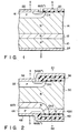
- a conductivity-modulation MOSFET (also called a "bipolar mode MOSFET") having a conventional vertical structure will be described with reference to Fig. 1, for the sake of easy understanding of the present invention.
- heavily-doped P type conductivity (P+ type) semiconductor layer 10 serves as a drain layer.
- N type buffer layer 12 and N ⁇ type base layer 14 are formed on drain layer 10.
- P type base layer 16 is formed in N ⁇ base layer 14 by diffusion.
- N+ type layer 18 serving as a source of the MOSFET is formed in P base layer 16, and defines, as channel region CH of the FET, a portion of P base layer 16 located between itself and N base layer 14.
- Gate electrode layer 20 insulatively covers N ⁇ base layer 14 and channel CH.
- Source electrode layer 22 is disposed on layer 14 so as to electrically short between P base layer 16 and N+ source layer 18.
- Drain electrode layer 24 is disposed on an opposite surface of P+ drain 10.
- MOSFET When gate electrode 20 is positively biased with respect to source electrode 22, the MOSFET is turned on.
- the physical mechanism of the MOSFET is as follows. When gate electrode 20 is applied with a positive voltage, channel region CH is inverted and electrons are injected from source 18 into N ⁇ base 14 through channel CH. When these electrons enter P+ drain 10 through N buffer layer 12, the PN junction of the MOSFET is forward-biased. In this case, holes are injected from P+ drain 10 to N base 14 through N buffer 12. Therefore, both the electrons and holes are stored or accumulated in N ⁇ base 14, thus inducing conductivity modulation.
- N ⁇ base 14 Even when the resistance of N ⁇ base 14 is set to be relatively high in order to obtain high withstand voltage characteristics, the resistance of N ⁇ base 14 is decreased upon turn-on of the MOSFET due to the conductivity modulation, so that a turn-on voltage is decreased.
- gate electrode 20 is biased to zero or negative with respect to source electrode 22, the inverted layer formed in channel region CH disappears, and the MOSFET is turned off.
- a vertical conductivity-modulation MOSFET having a double-gate structure has a characteristic feature in that it has second gate electrode G2 as a turn-off controlling electrode. More specifically, P base layer 32 and N+ type source layer 34 are formed in N ⁇ diffusion layer 30 in the same manner as in the prior art shown in Fig. 30. N+ source layer 34 defines, as first channel region CH1, a portion of P base 32 located between itself and N ⁇ base 30. Polysilicon layer 36 serving as first gate electrode G1 is insulatively provided above N ⁇ base layer 30 to be self-aligned with N+ source 34. Metal layer 38 serving as a source electrode electrically shorts P base layer 32 and N+ souce layer 34.
- N buffer layer 42 comprises N layers 42a and 42b (if N buffer layer 42 is separately formed as layers 42a and 42b, as illustrated in Fig. 2, this structure allows effective threshold value control of channel CH2).
- Polysilicon layer 40 serving as a second gate electrode is insulatively provided above one surface of N buffer layer 42.
- the other surface of N buffer layer 42 is connected to N ⁇ base layer 30.
- N buffer layer 42 serves to prevent generation of a punch-through phenomenon, and to increase a MOSFET withstand voltage.
- P type drain layer 44 is formed in N buffer layer 42.
- N+ type source diffusion layer 46 is formed in P type drain layer 44 by diffusion.
- N+ layer 46 defines, as second channel region CH2, a portion of P source 44 located between itself and N buffer 42.
- Metal layer 48 serving as a drain electrode electrically shorts between layers 44 and 46. As shown in Fig. 2, N+ layer 46, P drain 44, and N buffer 42 are formed by diffusion to be self-aligned with an end portion of second gate electrode 40.
- first gate electrode G1 is referred to as a "turn-on controlling gate electrode” or simply as an “ON gate” of the MOSFET hereinafter
- second gate electrode G2 is referred to as a "turn-off controlling gate electrode” or simply as an “OFF gate” hereinafter.
- the conductivity-modulation MOSFET is turned on, when turn-on controlling gate electrode G1 is positively biased with respect to source electrode S, and turn-off controlling gate electrode G2 is biased to a zero or negative potential with respect to drain electrode D.
- the physical mechanism associated with the turn-on of the MOSFET is substantially the same as that in the prior art shown in Fig. 1. More specifically, in a turn-on mode of the MOSFET, OFF gate G2 is biased to a zero or negative potential. Therefore, second channel region CH2 is kept nonconductive. N ⁇ buffer 30 is disconnected from drain electrode D in the same manner as in N buffer 12 shown in Fig. 1.
- turn-on controlling gate electrode G1 When the MOSFET is to be turned off, turn-on controlling gate electrode G1 is biased to a zero or negative potential with respect to source electrode S, and turn-off controlling gate electrode G2 is positively biased with respect to drain electrode D.
- channel region CH1 is rendered nonconductive, and channel region CH2 is inverted and rendered conductive. Since channel region CH1 is rendered nonconductive, injection of electrons from N+ source 34 into N base 30 is inhibited.
- channel region CH2 is rendered conductive, N+ source 46 is electrically conducted to N buffer 42, so that drain electrode D shorts between N buffer 42 and P drain 44, thereby temporarily forming a "shorted anode structure". In this case, a current gain of the PNP transistor becomes zero.
- Electrons accumulated in the device are rapidly discharged through N buffer 42, channel CH2, and N+ source 46. Holes migrate into source electrode layer 38 through P base 32. This state is substantially equivalent to a state wherein P and N bases 32 and 30 are reverse-biased.
- gate G2 is activated to invert channel CH2, and N buffer layer 30 is electrically shorted with electrode layer 10 constituting drain electrode D, thereby providing the "shorted anode structure". Therefore, the turn-off speed of the MOSFET can be increased.
- the carrier lifetime need not be shortened, the current gain of the PNP transistor in the turn-on state of the MOSFET can be increased.
- the thickness of N base diffusion layer 30 is increased, its forward voltage drop can be kept small, and the turn-on voltage of the MOSFET can be maintained low. Therefore, the conflicting problems which the conventional conductivity-modulation MOSFET suffers can be simultaneously solved.
- the device structure in the turn-off mode is equivalent to a diode constituted by P and N bases 16 and 14.
- the MOSFET has a reverse-conducting diode therein (N buffer 42 serves as an N emitter to decrease a forward voltage drop of the reverse-conducting diode).
- N buffer 42 serves as an N emitter to decrease a forward voltage drop of the reverse-conducting diode.
- a current flows through a path constituted by source electrode 38, P base 32, N base 30, N buffer 42, channel CH2, N+ source 46, and drain electrode layer 48.
- the presence of the diode is particularly effective when the device structure of the present invention is applied to a high-voltage MOSFET which deals with 2,000 volts or higher.
- the "shorted anode structure" is temporarily formed in the device only when it is driven to be turned off.
- the N buffer layer 42 is electrically shorted with drain electrode D, carriers (electrons, in this case) accumulated in N ⁇ base 30 in a turn-off mode can be rapidly disappeared, since the current gain of the above-mentioned PNP transistor is reduced to zero and hence the tail current components of the turn-off current can be very small.
- the "shorted anode structure" is always formed in the MOSFET throughout turn-on/off control, turn-on characteristics may be impaired.
- second gate electrode G2 is provided as the OFF gate, and during turn-on control of the MOSFET, N buffer 42 is forcibly disconnected from drain electrode D, thereby disappearing the "shorted anode structure".
- applications of a turn-on/off controlling voltage to gates G1 and G2 can be delayed from one another so that OFF gate G2 is turned on faster than ON gate G1.
- a few microseconds before a voltage application to ON gate G1 more preferably, 1 ⁇ s or more before a voltage application to ON gate G1, OFF gate G2 is applied with a positive voltage.
- An application of a positive voltage for turn-off control allows a further increase in the turn-off speed of the conductivity-modulation MOSFET. The reason therefor is as follows.
- Fig. 3 is a graph showing a calculated inductive turn-off waveform of the aforementioned conductivity-modulation MOSFET device. 0.8 ⁇ s and 0.65 ⁇ s fall-time could be obtained by adjusting the timing for causing N-channel anode short. As shown in Fig. 3, turn-off controlling gate G2 was positively biased approximately 2 ⁇ s before turning off the device or reducing the turn-on controlling gate G1 bias. By creating the N-channel shunt, a few microseconds before turning off the device, the excess carriers inside the device were effectively removed, thus realizing a short fall-time.
- Fig. 4 shows the electron density distribution change corresponding to Fig. 3. It is clearly seen from Fig.
- Fig. 5 shows a sectional structure of a conductivity-modulation MOSFET according to a second embodiment of the present invention.
- the same reference numerals in Fig. 5 denote the similar portions as in Fig. 2: a detailed description thereof will be omitted.
- N buffer layer is formed, and therefore, the source and drain structures of the MOSFET are symmetrical with each other on the front and rear surfaces of the wafer.
- One N type semiconductor layer 50 constitutes an N base.
- P base diffusion layer 32 and P source diffusion layer 44 are symmetrically formed on the opposing surfaces of N base layer 50.
- N+ source layers 34 and 46 are symmetrically formed, thus defining symmetrical channels CH1 and CH2.
- deep P+ diffusion layer 52 is additionally formed in P drain layer 44 located beneath drain electrode layer 48.
- P+ layer 52 is deeper than P drain 44.
- P+ layer 52 overlaps N+ layer 46. Addition P+ layer 52 improves injection efficiency of holes on the drain side of the MOSFET.
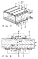
- Fig. 7 is a perspective view of a MOSFET having a double-gate structure according to a fourth embodiment of the present invention, wherein an upper source electrode pattern is shifted from a lower drain electrode pattern through 90 degrees.
- ON-gate electrode layers (these are designated by identical numerals "36" in Fig. 7) and source electrode layers (these are denoted by identical numerals "38” in Fig. 7) are alternately arranged on the the upper surface of a wafer, i.e., the top surface of N base 30, and slit-like elongated parallel grooves are defined between these layers 36 and 38.
- These layers 36 and 38 extend along one direction.
- P base layers 32 and N+ source layers 34 are elongated along the extending direction of layers 36 and 38.
- layers 36 or 40 are covered by an insulative layer such as an SiO2 film, and layers 38 or 48 are formed on the entire surface of the insulative layer, in practice.
- OFF-gate electrode layers (these are designated by identical numerals "40" in Fig. 7) and drain electrode layers (these are denoted by identical numerals "48” in Fig. 7) are alternately arranged on the rear surface of the wafer, i.e., on the surface of N buffer 42, slit-like parallel elongated grooves are defined between these layers 36 and 38. These layers 40 and 48 extend in a direction shifted from the extending direction of layers 36 and 38 by 90 degrees. P drain layers 44 and N+ diffusion layers 46 formed therebelow are elongated along the extending direction of layers 40 and 48. If such an electrode pattern is adopted, local concentration of a turn-on current inside the wafer is moderated, and a current distribution can be made uniform.
- upper source electrode pattern extends in the same direction as that of a lower drain electrode pattern and is shifted therefrom by half an interval (pitch).
- source electrodes 38 and drain electrodes 48 are inhibited from directly opposing each other, and ON-gate electrodes 36 and OFF-gate electrodes 40 are also inhibited from directly opposing each other.
- ON-gate electrode layer 36 faces drain electrode layer 48
- OFF-gate electrode layer 40 faces source electrode layer 38.
- electrode layers are fabricated so that the relation among width Lg1 of ON-gate electrode layer 36, source width Ls, width Lg2 of OFF-gate electrode layer 40, and drain width Ld satisfies the following inequality: (Ls + Lg1) ⁇ (Lg2 + Lg) ...(1)
- electrode layers are fabricated so that the relation among width Lg1 of ON-gate electrode layer 36, source width Ls, width Lg2 of OFF-gate electrode layer 40, and drain width Ld satisfies the following inequality: (Ls + Lg1) > (Lg2 + Lg) ...(2)
- OFF-gate electrode layer 60 has a double-layered structure of polycrystalline silicon layer 62 and metal layer 64.
- a gate electrode layer has an increased area.
- a gate layer comprises a polycrystalline layer having a relatively high resistivity, a gate resistance is undesirably increased.
- metal layer 64 is stacked on polycrystalline gate layer 62 to form double-layered gate layer 60 having a reduced resistance.
- Double-layered gate layer 60 is buried deep in N buffer layer 42 to prevent the top surface of double-layered gate layer 60 from projecting from N buffer layer 42. Therefore, the drain side of the MOSFET device can be stably mounted on a known base plate (not shown).
- ON-gate electrode layer 36 is covered with insulation layer 66.
- Metal layer 68 is formed on lightly-doped N type base layer 30 ⁇ so as to cover ON-gate electrode layers 36.
- Metal layer 68 serves as a common source electrode of the MOSFET.
- Metal layer 72 is formed on layer 42 to cover OFF-gate electrode 40. Metal layer 72 serves as a common drain electrode of the MOSFET.
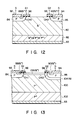
- Fig. 12 is a cross-sectional view of a main part of a conductivity-modulation MOSFET having a horizontal double-gate structure (which is also an embodiment of the present invention).
- the source and drain of the MOSFET are formed on a single surface of N ⁇ base layer 80, according to this embodiment.
- Lightly-doped N type (N ⁇ type) silicon wafer 80 is used as an N ⁇ base layer of the MOSFET.
- Heavily-doped N type (N+ type) buffer layer 82 is formed on one surface of silicon wafer 80.
- Electrode layer 82 is formed on buffer layer 82.
- P type diffusion layers 84 and 86 are formed on the other surface (front surface) of silicon wafer 80.
- P type diffusion layers 84 and 86 serve as P base and P drain layers respectively.
- N+ type layers 88 and 90 are respectively formed in P base and P drain layers 84 and 86 to define channel regions CH1 and CH2.
- Source electrode layer 92 is deposited on wafer 80 to render layers 84 and 86 electrically conductive to each other.
- Drain electrode layer 94 is deposited on wafer 80 to render layers 86 and 90 electrically conductive to each other.
- First gate electrode layer 96 serving as an ON-gate insulatively covers channel CH1, and constitutes a turn-on controlling transistor of the MOSFET.
- P ⁇ type silicon wafer 100 is used in place of N ⁇ type silicon wafer 80 in the embodiment shown in Fig. 12.
- Heavily-doped (P+ type) buffer layer 102 is formed on one surface of P ⁇ type silicon wafer 100. Since P ⁇ type silicon wafer 100 is used, N type diffusion layer (drain isolation layer) 104 is necessary for electrically insulating P type diffusion layer 86 from wafer 100.
- Layer 104 can be formed in a self-aligned manner with layers 90 and 86, and serves as an N buffer, which acts as an N emitter to decrease a voltage drop generated when the device operates as a reverse conducting diode.
- Lightly-doped N type (N ⁇ type) diffusion layer 106 is formed shallow in the surface portion of wafer 100, and can be connected to layer 104.
- Shallow N ⁇ type diffusion layer 106 serves as an N base layer to which electrons are injected from first N+ source diffusion layer 88. It was experimentally demonstrated by the present inventors that when shallow diffusion layer 106 had an impurity concentration of about 5 x 10¹¹ to 4 x 10¹²/cm2, the withstanding voltage of the transistor structure was maximized, and a sufficiently low turn-on resistance could be obtained.
- a two-dimensional pattern of the source and drain of the MOSFET should be carefully designed such that a depletion layer in a junction portion at which a reverse bias voltage is applied is uniformly expanded, and a deviated internal electric field distribution is minimized in that portion.
- the two-dimensional pattern of the source and drain of the MOSFET should be carefully designed so that necessity of addition of a special passivation to each element boundary portion is eliminated.
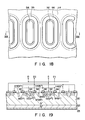
- Embodiments of two-dimensional patterns of conductivity-modulation MOSFETs having horizontal double-gate structure which can fully meet the requirements on device design will be presented and explained below.
- drain isolation diffusion layer 104 is formed on a front surface portion of wafer 100 to define island layers.
- one island drain isolation diffusion layer 104 is indicated by broken line.
- P drain diffusion layer 86 is formed in each drain isolation diffusion layer 104 (see Fig. 15).
- Second N+ type source layer 90 is formed in layer 86 to have an elliptical ring shape.
- Heavily-doped diffusion layer 110 of P type conductivity is formed deep in the central region of each P drain diffusion layer 86.
- Shallow N ⁇ diffusion layer 106 two-dimensionally surrounds island drain isolation diffusion layer 104.
- N ⁇ diffusion layer 106 is connected to each island drain isolation diffusion layer 104, as shown in Fig. 15.
- Drain electrode 94 is directly formed on the surface of wafer 100 to overlap P+ type layer 110. Drain electrode 94 has an elliptical shape, as clearly illustrated in Fig. 14.
- OFF-gate electrode layer 98 is insulatively formed above wafer 100 to surround drain electrode 94.
- OFF-gate electrode layer 98 has an elliptical ring shape.
- ON-gate electrode layer 96 is insulatively formed above wafer 100 to surround OFF-gate electrode layer 98 and to have an elliptical ring shape.
- Conductive layer 92 serving as source electrode S two-dimensionally surrounds ON-gate electrode layers 96 formed on wafer 100 in the manner as described above, as shown in Fig. 14.
- P base layer 84 formed on the surface of wafer 100 two-dimensionally surrounds island diffusion layers 104 each of which includes drain layer 86 (see Fig. 14). Electrode layer 83 formed on the rear surface of wafer 100 is, e.g., grounded.
- P base layer 84 is designed to surround island drain regions 86. Therefore, when one MOSFET element is isolated from wafer 100, or when one element is electrically insulated from other elements formed on single wafer 100, an element boundary is formed in each P base layer 84, thus facilitating setting of passivation in each P base layer 84.
- a junction portion which is reverse-biased in the turn-off mode of the MOSFET is formed between P ⁇ wafer 100 and a diffusion layer portion comprising N type drain isolation diffusion layer 104 surrounding P drain 86 and shallow N ⁇ layer 106 provided around layer 104.
- a depletion layer radially expands outwardly from the elliptical diffusion layer portion in wafer 100, so that local concentration of an electric field in wafer 100 can be satisfactorily suppressed. Therefore, operation reliability of the MOSFET can be improved.
- An embodiment illustrated in Figs. 16 and 17 has wafer 80 of an N type conductivity.
- N type wafer 80 When N type wafer 80 is used as an N base, a junction portion to which a reverse bias voltage is applied in a turn-off mode of the MOSFET is formed between P base diffusion layer 84 and N type wafer 80. Therefore, in contrast to the embodiment shown in Figs. 14 and 15, each P base layer 84 is formed in N type wafer 80 to have an elliptical island shape, as shown in Fig. 16.
- P drain diffusion layer 86 and N type diffusion layer 112 including layer 86 are formed continuously with wafer 80 so as to two-dimensionally surround elliptical island P base layers 84.
- N type layer 112 prevents a depletion layer formed between each P base layer 84 and N type wafer 80 from reaching P drain 86, and hence, prevents a decrease in withstand voltage of the MOSFET.
- Second N+ diffusion layer 88 is formed in each elliptical island P base layer 84 to have a two-dimentionally elliptical ring-shape.
- Source electrode layer 92 is deposited on wafer 80, located at the central flat region of corresponding island P base layer 84, and has an elliptical shape (see Fig. 16).
- Electrode layer 96 serving as ON gate G1 is formed on wafer 80 to surround each source electrode layer 92.
- Electrode layer 98 serving as OFF gate G2 surrounds ON-gate electrode layer 96.
- drain electrode layer 94 is continuously formed on wafer 80 to surround OFF-gate electrode layers 98.
- Electrode layer 83 formed on the rear surface of wafer 80 is set at a drain potential.
- both source and drain regions alternately arranged on wafer 80 are formed to have an elliptical shape, as shown in Fig. 18.
- Each source electrode layer 92 is formed on wafer 80 to be located on the central flat region of corresponding island P base layer 84 and to have an elliptical shape (see Fig. 16).
- ON-gate electrode layer 96 surrounds source electrode layer 92.
- Each drain electrode layer 94 is formed on wafer 80, located on the central flat region of corresponding island P drain diffusion layer 86, and has an elliptical shape (see Fig. 16).
- OFF-gate electrode layer 98 surrounds drain electrode layer 94.
- N+ diffusion layer 114 is continuously formed on the surface portion of wafer 80 to surround the source and drain regions.
- a drain potential is applied to N type wafer 80 through P drain 86 and P+ layer 110 which are forward-biased. Therefore, continuous N+ diffusion layer 114 is formed so that a necessary potential can be applied to the junction portion of each island P base layer 84 without a drain electrode provided on one entire surface of wafer 80 in the embodiment shown in Figs. 16 and 18.
- both source and drain regions alternately arranged on wafer 80 are formed to have an elliptical shape in the same manner as in the embodiment shown in Figs. 18 and 19 (see Fig. 19).
- N type diffusion layer 112 in which drain regions are formed is continuously formed on the entire surface of wafer 80, as shown in Fig. 20.
- N type diffusion layer 112 has the same function as N+ diffusion layer 114 shown in Figs. 18 and 19. With this structure, the same effects as in the above embodiments can be provided.
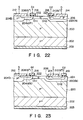
- Fig. 22 is a cross-sectional view of a main part of a conductivity-modulation MOSFET having a horizontal double-gate structure according to an embodiment of the present invention.
- the source and drain of the MOSFET are formed on the front surface of P ⁇ type wafer substrate 200 and adjacent to each other.
- Wafer 200 is used as a P base layer of the MOSFET.
- P+ type layer 202 is formed on the rear surface portion of wafer 200.
- Electrode layer 203 is formed on layer 202.
- P type diffusion layers 204 and 206 are formed on the front surface of silicon wafer 200.
- P type diffusion layers 204 and 206 respectively serve as P base and P drain layers.
- Layer 204 consists of P type diffusion layer 204a and relatively deep P+ type diffusion layer 204b.
- N+ type diffusion layer 208 is formed in P base diffusion layer 204.
- Layer 208 defines channel region CH1 in layer 204a.
- N+ type diffusion layer 210 is formed in P drain layer 206, and defines channel region CH2 in layer 206.
- Source electrode layer 212 is deposited on wafer 200 to render layers 204b and 208 electrically conductive to each other, and drain electrode layer 214 is deposited on wafer 200 to render layers 206 and 210 electrically conductive to each other.
- First gate electrode layer 216 serving as an ON-gate insulatively covers channel CH1 and constitutes a turn-on controlling transistor of the MOSFET.
- Second gate electrode layer 218 serving as an OFF-gate insulatively covers channel CH2 and constitutes a turn-off controlling transistor of the MOSFET.
- N type diffusion layer 220 is formed on the front surface portion of wafer 200 to include P drain layer 206 therein.
- N type diffusion layer 220 serves as an N buffer.
- N ⁇ type diffusion layer 222 which is connected to buffer 220 and extends immediately below gate G1 is formed on the front surface portion of wafer 200.
- Layer 222 serves as an N base.
- N type impurity ions are implanted in channel region CH2 which is defined on the surface portion of wafer 200 so as to be located below second gate electrode 218 which serves as OFF gate G2, as clearly illustrated in Fig. 22.
- N+ drain 210 is conducted to N ⁇ type isolation layer 220 through N ⁇ type diffusion section (to be referred to as an "N bypass layer” hereinafter) 224 of channel region CH2. Since the impurity concentration of the N ⁇ type diffusion section is relatively Very low (e.g., about 1 x 10¹¹ to 1 x 10¹³/cm2), a conductance between N+ drain 210 and N ⁇ type isolation layer 220 is relatively low, and a lateral resistance therebetween is relatively high. In this sense, N+ drain 210 is half-conducted to N base 220 through N bypass layer 224 of channel region CH2. Alternatively, a turn-off controlling switch section having OFF gate G2 is normally rendered half-conductive.
- the turn-off controlling switch section having OFF gate G2 which is rendered conductive in the turn-off mode of the conductivity-modulation MOSFET is rendered half-conductive in other operation modes.
- a positive voltage is applied to source electrode 212 in in order to turn on the MOSFET, electrons are injected from N+ source 208 into N base 222. These electrons flow into N+ layer 210 through N bypass layer 224.
- a potential difference is generated by the lateral resistance of N bypass layer 224.
- the lateral potential difference forward-biases the PN junction portion between P drain 206 and N buffer 220. Upon forward-biasing, holes are injected from P drain 206 into N base 222. N base 222 is thus subjected to conductivity modulation, and the MOSFET can be turned on at a relatively low turn-on controlling voltage.
- N bypass layer 224 for half-conducting N+ drain 210 and N base 220 is provided to channel region CH2.
- the potential difference for forward-biasing the PN junction portion of P drain 206 in the turn-on mode of the MOSFET is generated in N bypass layer 224.
- the lateral resistance of N bypass layer 224 can be desirably increased by controlling the concentration of impurities injected into channel region CH2. Therefore, even if the impurity concentration of N buffer 220 is increased to relatively high, a desired high withstand voltage of the element can be maintained. This contributes to realization of a conductivity-modulation MOSFET having good turn-off characteristics (capable of high-speed turn-off switching) and a high withstand voltage.
- drain electrode 214 and OFF gate electrode 218 on wafer 200 are reversed to those in the embodiment shown in Fig. 22. More specifically, gate electrode 218 of a turn-off controlling switch section is formed outside N+ layer 210 and separated from N base 222. Therefore, channel region CH2, which is located below electrode layer 218 serving as OFF gate G2 and in which N bypass layer 224 is formed, is also defined outside N+ layer 210, as shown in Fig. 23. With this structure, the same effects as described above can be provided.
- the impurity concentration of channel region CH2 defined in P drain layer 86 cannot exceed 5 x 10¹⁶ to 1 x 10¹⁷/cm3 in consideration of threshold voltage level Vth of the turn-off controlling switch section.
- effective conductivity modulation of the MOSFET cannot always be performed, since it cannot be expected that holes are effectively injected from P drain 86.
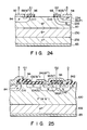
- Modifications suitable for a case wherein injection efficiency of holes from the P drain layer must be improved in the conductivity-modulation MOSFET having the horizontal double-gate structure will be presented below.
- P ⁇ type diffusion layer 230 and P+ type diffusion layer 232 are formed on the rear surface portion of N type wafer 80.
- Second N+ diffusion layer 90 and shallow P+ type diffusion layer 234 are formed in P drain layer 86 formed on the front surface portion of N type wafer 80.
- P+ layer 234 overlaps N+ diffusion layer 90 and is adjacent to channel region CH2, as illustrated in Fig. 24.
- Deep N type diffusion layer 236 is formed in wafer 80 to surround P drain layer 86. Since shallow P+ type diffusion layer 234 is additionally formed in P drain layer 86, the injection efficiency of holes from the P drain can be effectively improved without increasing the impurity concentration of channel region CH2.
- electrode layer 98 serving as OFF gate G2 is insulatively provided above P ⁇ type wafer 100 so as to be distant from the source region of the device.
- Shallow P+ type diffusion layer 240 is formed in P drain layer 86 on the side of the source region.
- Drain electrode layer 242 is formed on wafer 100 to be in electrical contact with N+ layer 90 and P+ layer 240 in P drain layer 86, as shown in Fig. 25.
- N buffer layer 104, P drain 86, and N+ layer 90 can be easily fabricated in wafer 100 by a triple diffusion technique using the edge portion of one end of OFF gate electrode layer 98 as one end of a window opening of a diffusion mask.
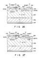
- the conductivity-modulation MOSFETs having the double-gate structure have been disclosed in the embodiments of the present invention as described above, the high-speed turn off controlling technique in the conductivity-modulation MOSFETs of the present invention can also be realized in a shorted anode MOSFET having a single-gate structure. Embodiments of such conductivity-modulation MOSFETs will be described below.
- a conductivity-modulation MOSFET shown in Fig. 26 is substantially the same multilayered structure as that shown in Fig. 22, except that turn-off controlling gate G2 is omitted from the MOSFET shown in Fig. 26.
- the same reference numerals in Fig. 26 denote the same portions as in Fig. 22, and a detailed description thereof will be omitted.
- N buffer layer 220 is constantly half-connected to drain electrode layer 214 through channel region CH2 in both turn-on and turn-off modes of the conductivity-modulation MOSFET.
- Electrons accumulated in N base 222 are discharged into N+ layer 210 through N bypass layer 224, and holes accumulated in N base 222 are discharged into source electrode 212 through P base 204.
- the conductivity-modulation MOSFET is turned off.
- the potential difference for forward-biasing the PN junction occurs in N bypass layer 224, and the lateral resistance for causing the potential difference can be easily controlled by adjusting the impurity concentration of the N bypass layer. Therefore, even if the concentration of the N buffer is desirably increased, a withstanding voltage of the element can be increased without increasing the width of the N bypass layer.
- N bypass layer 224 is formed outside drain electrode 214.
- dielectric element isolation film 250 is formed on supporting substrate 254, and buried isolation layer 252 is formed on film 250, as shown in Fig. 28.
- the above structural feature is applied to a vertical shorted anode MOSFET having a single-gate structure, wherein N bypass layer 224 is formed on an opposite surface portion of a substrate.
- diffusion layer 234 is added. A two-dimensional pattern of the diffusion layer suitable for this element structure will be explained below.
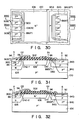
- FIG. 30 has the same the basic structure as in the embodiment shown in Fig. 13, wherein N drain layer 104 is formed in P ⁇ type silicon wafer 100, and P drain diffusion layer 86 and second N+ source 90 are formed in layer 104.
- N drain layer 104 is formed in P ⁇ type silicon wafer 100
- P drain diffusion layer 86 and second N+ source 90 are formed in layer 104.
- electrodes provided to respective portions are omitted, and only a diffusion layer pattern is visible.
- Fig. 31 shows a sectional structure taken along a line XXXI - XXXI in Fig. 30, and Fig. 32 shows a sectional structure taken along a line XXXII - XXXII in Fig. 30.
- the same reference numerals denote the same portions as in Fig. 13 or 24, and a detailed description thereof will be omitted.
- second N+ source diffusion layer 90 in such a manner that it is divided into a plurality of layers by P type diffusion layers 300.
- P+ layers 300 serve as a part of a drain diffusion layer.
- second channel region CH2 below OFF controlling gate electrode 98 is divided into sub channels CH2-1 (see Fig. 31) which contribute to a transistor operation, and sub-channels CH2-2 (see Fig. 32) which do not contribute to the transistor operation. These sub-channels CH2-1 and CH2-2 are alternately arranged when viewed from the top. Since second N+ source diffusion layer 90 is divided as described above, injection efficiency of holes from P drain 86 when the MOSFET is rendered conductive can be improved, and hence, the ON voltage of the MOSFET can be decreased.
- high resistance layer 302 is insulatively provided above a substrate to connect first and second gate electrodes 96 and 98 to each other.
- MOSFET MOSFET
- a very small current flows through layer 302, and an electric field inside N ⁇ buffer layer 106 is moderated, thus preventing local concentration of an internal electric field.
- first N+ source layer 88 is formed on a side opposite to channel region CH1 to have a three-dimensional pattern. Therefore, electrical contact characteristics of source electrode 92 with respect to first N+ source layer 88 can be improved.
- second N+ source diffusion layer 90 is integrally formed, and P+ type layer 300 serving as a part of a drain diffusion layer has a three-dimensional pattern. More specifically, P+ type layer 300 has recess portion 300a whose end portion is located inside N+ source diffusion layer 90, and projection portion 300b whose end portion extends to channel region CH2 below second gate electrode 98, as shown in Fig. 34. These rectangular edge portions 300a and 300b are alternately arranged, as clearly illustrated in Fig. 33. With this structure, second channel region CH2 can be divided into sub-channels CH2-1 and CH2-2. Therefore, injection efficiency of holes from the P drain in the ON MOSFET can be improved, and a low ON voltage can be obtained.
- second N+ source diffusion layer 90 is formed on an end portion (of P drain diffusion layer 86) farther from P base diffusion layer 84a in P drain diffusion layer 86.
- P+ layer 300 is formed on an end portion of P drain diffusion layer 86 closer to P base diffusion layer 84a.
- high-resistance N diffusion layers 304 are formed in N drain isolation layer 104 to partially overlap P+ type layers 300. These N type layers 304 are linearly arranged at equal intervals on an a portion opposite to channel region CH2, thus electrically shorting second N+ source diffusion layer 90 to N drain isolation layer 104. With this structure, electrons are discharged through channel CH2, and are also discharged through high-resistance N diffusion layers 304 when the MOSFET is turned off. Therefore, the switching speed of the device can be increased. Since P+ layers 300 are located on the side opposite to channel CH2 and closer to N ⁇ buffer layer 106, injection efficiency of holes from P drain 86 upon turn-on of the MOSFET can be improved, and hence, the turn-on voltage can be decreased.
- N+ diffusion layer 306 is provided to electrically short together first end portions of high-resistance layers 304.
- N+ diffusion layer 306 is formed in N drain isolation layer 104 and parallel to second N+ source diffusion layer 90, as best illustrated in Fig. 40.
- High-resistance layers 304 for shorting second N+ source diffusion layer 90 and N drain isolation layer 104 are connected to each other by N+ diffusion layer 306, so that electrons can be uniformly discharged into drain electrode 94 when the MOSFET is turned off. Therefore, the switching speed of the element can be increased. Since N type layers 304 has a high resistance, passing of electrons through N type layers 304 can be suppressed. In this case, most electrons pass through P drain layer 86. Therefore, holes equivalent to passing electrons are injected, thus providing good conductivity-modulation action.
- short holes 308 are formed in N+ layer 90 formed in P drain layer 86.
- N buffer 104 is partially shorted to N+ layer 90 through these short holes 308.
- the shape of these short holes 308 may be arbitrarily determined. Electrons accumulated in N base 106 are discharged into drain electrode 94 through short holes 308, and hence, a turn-off time of the device can be shortened. It can be regarded that this structure has a PNPN junction thyristor structure when viewed from the source of the device, and reverse conductive characteristics having a low turn-on voltage can be provided.
- Figs. 44 and 45 show other modifications of the present invention.
- P ⁇ type diffusion layers 314 and 316 are formed in a region surrounded by SiO2 layer 312.
- Shallow N ⁇ type diffusion layer (N base) 318 and deep N type diffusion layer (N buffer) 320 are formed in P ⁇ layer 316.
- P type layer 322, P+ type layer 324, and N+ layer 325 are formed in layer 320, and anode electrode layer 326 are formed on these layers.
- P type layer 328 is formed in P ⁇ layer 316, and N type layer 330, N+ type layer 332, and P+ type layers 334a and 334b are formed in layer 328.
- Cathode electrode C is in electrical contact with layers 332 and 334.
- First and second gate electrodes G1 and G2 are insulatively provided above the wafer. With this structure, when second gate electrode G2 and the anode electrode are shorted and a positive voltage is applied to first gate electrode G1, the thyristor constituted by layers 332, 328, 316, 320, and 324 is turned on. When negative voltages are applied to the both of second gate electrodes G1 and G2, the thyristor is turned off.
- Fig. 45 shows a case wherein the thyristor structure is applied to a normal double-gate device.
Landscapes
- Engineering & Computer Science (AREA)
- Microelectronics & Electronic Packaging (AREA)
- Power Engineering (AREA)
- Physics & Mathematics (AREA)
- Ceramic Engineering (AREA)
- Condensed Matter Physics & Semiconductors (AREA)
- General Physics & Mathematics (AREA)
- Computer Hardware Design (AREA)
- Insulated Gate Type Field-Effect Transistor (AREA)
- Bipolar Transistors (AREA)
Applications Claiming Priority (9)
| Application Number | Priority Date | Filing Date | Title |
|---|---|---|---|
| JP4130987 | 1987-02-26 | ||
| JP41309/87 | 1987-02-26 | ||
| JP4130987 | 1987-02-26 | ||
| JP110743/87 | 1987-05-08 | ||
| JP11074387 | 1987-05-08 | ||
| JP11074387 | 1987-05-08 | ||
| JP62304634A JPH0821713B2 (ja) | 1987-02-26 | 1987-12-03 | 導電変調型mosfet |
| JP304634/87 | 1987-12-03 | ||
| JP30463487 | 1987-12-03 |
Publications (3)
| Publication Number | Publication Date |
|---|---|
| EP0280535A2 true EP0280535A2 (fr) | 1988-08-31 |
| EP0280535A3 EP0280535A3 (fr) | 1990-10-10 |
| EP0280535B1 EP0280535B1 (fr) | 2001-07-18 |
Family
ID=27290772
Family Applications (1)
| Application Number | Title | Priority Date | Filing Date |
|---|---|---|---|
| EP88301592A Expired - Lifetime EP0280535B1 (fr) | 1987-02-26 | 1988-02-24 | Transistor à effet de champ du type MOS à modulation de la conductivité |
Country Status (4)
| Country | Link |
|---|---|
| US (1) | US4980743A (fr) |
| EP (1) | EP0280535B1 (fr) |
| JP (1) | JPH0821713B2 (fr) |
| DE (1) | DE3856480T2 (fr) |
Cited By (18)
| Publication number | Priority date | Publication date | Assignee | Title |
|---|---|---|---|---|
| EP0361589A1 (fr) * | 1988-09-22 | 1990-04-04 | Koninklijke Philips Electronics N.V. | Transistors bipolaires latéraux à grille isolée comportant une anode fractionnée |
| EP0380249A2 (fr) * | 1989-01-21 | 1990-08-01 | LUCAS INDUSTRIES public limited company | Transistor bipolaire à grille isolée |
| US5040042A (en) * | 1989-04-28 | 1991-08-13 | Asea Brown Boveri Ltd. | Bidirectional semiconductor component that can be turned off |
| US5091766A (en) * | 1989-10-23 | 1992-02-25 | Mitsubishi Denki Kabushiki Kaisha | Thyristor with first and second independent control electrodes |
| EP0476815A2 (fr) * | 1990-08-18 | 1992-03-25 | Mitsubishi Denki Kabushiki Kaisha | Thyristor et méthode de fabrication |
| US5105243A (en) * | 1987-02-26 | 1992-04-14 | Kabushiki Kaisha Toshiba | Conductivity-modulation metal oxide field effect transistor with single gate structure |
| EP0497577A2 (fr) * | 1991-01-31 | 1992-08-05 | Kabushiki Kaisha Toshiba | Dispositif à semiconducteur à haute tension de claquage |
| US5155563A (en) * | 1991-03-18 | 1992-10-13 | Motorola, Inc. | Semiconductor device having low source inductance |
| EP0526037A1 (fr) * | 1991-07-25 | 1993-02-03 | Hitachi, Ltd. | Transistor bipolaire latéral à grille isolée |
| US5194394A (en) * | 1989-10-23 | 1993-03-16 | Mitsubishi Denki Kabushiki Kaisha | Thyristor and method of manufacturing the same |
| EP0594111A1 (fr) * | 1992-10-19 | 1994-04-27 | Fuji Electric Co., Ltd. | Transistor MIS haute-tension et dispositif semi-conducteur |
| EP0389942B1 (fr) * | 1989-03-29 | 1994-08-17 | Asea Brown Boveri Ag | Dispositif semi-conducteur à tension de blocage élevée |
| US5343067A (en) * | 1987-02-26 | 1994-08-30 | Kabushiki Kaisha Toshiba | High breakdown voltage semiconductor device |
| US5574298A (en) * | 1994-06-30 | 1996-11-12 | Texas Instruments Incorporated | Substrate contact for gate array base cell and method of forming same |
| EP0760529A2 (fr) * | 1995-08-24 | 1997-03-05 | Kabushiki Kaisha Toshiba | IGBT latéral |
| US5710444A (en) * | 1992-12-28 | 1998-01-20 | Daimler-Benz Aktiengesellschaft | Insulated gate bipolar transistor having a coupling element |
| EP0634796B1 (fr) * | 1993-07-12 | 2000-10-04 | Kabushiki Kaisha Toshiba | Transistor bipolaire à grille isolée |
| CN100372127C (zh) * | 2003-12-01 | 2008-02-27 | 三洋电机株式会社 | 半导体装置 |
Families Citing this family (27)
| Publication number | Priority date | Publication date | Assignee | Title |
|---|---|---|---|---|
| JP2876625B2 (ja) * | 1989-06-07 | 1999-03-31 | 日本電気株式会社 | 導電変調型電界効果トランジスタ |
| JPH03104169A (ja) * | 1989-09-18 | 1991-05-01 | Mitsubishi Electric Corp | 半導体装置 |
| US5155562A (en) * | 1990-02-14 | 1992-10-13 | Fuji Electric Co., Ltd. | Semiconductor device equipped with a conductivity modulation misfet |
| US5548133A (en) * | 1994-09-19 | 1996-08-20 | International Rectifier Corporation | IGBT with increased ruggedness |
| JP4357127B2 (ja) | 2000-03-03 | 2009-11-04 | 株式会社東芝 | 半導体装置 |
| EP1401021A4 (fr) * | 2001-05-25 | 2008-03-26 | Mitsubishi Electric Corp | Dispositif semi-conducteur de puissance |
| JP4566470B2 (ja) * | 2001-07-17 | 2010-10-20 | 三菱電機株式会社 | 絶縁ゲート型バイポーラトランジスタ |
| JP5087818B2 (ja) * | 2005-03-25 | 2012-12-05 | 日亜化学工業株式会社 | 電界効果トランジスタ |
| JP5245157B2 (ja) * | 2008-06-03 | 2013-07-24 | 独立行政法人産業技術総合研究所 | 半導体双方向スイッチング装置 |
| US9742385B2 (en) | 2013-06-24 | 2017-08-22 | Ideal Power, Inc. | Bidirectional semiconductor switch with passive turnoff |
| US9799731B2 (en) | 2013-06-24 | 2017-10-24 | Ideal Power, Inc. | Multi-level inverters using sequenced drive of double-base bidirectional bipolar transistors |
| US9029909B2 (en) | 2013-06-24 | 2015-05-12 | Ideal Power Inc. | Systems, circuits, devices, and methods with bidirectional bipolar transistors |
| US9355853B2 (en) | 2013-12-11 | 2016-05-31 | Ideal Power Inc. | Systems and methods for bidirectional device fabrication |
| US11637016B2 (en) | 2013-12-11 | 2023-04-25 | Ideal Power Inc. | Systems and methods for bidirectional device fabrication |
| US9444449B2 (en) | 2014-11-06 | 2016-09-13 | Ideal Power Inc. | Circuits, methods, and systems with optimized operation of double-base bipolar junction transistors |
| JP2016171231A (ja) * | 2015-03-13 | 2016-09-23 | 株式会社東芝 | 半導体装置および半導体パッケージ |
| JP7027287B2 (ja) * | 2018-09-19 | 2022-03-01 | 株式会社東芝 | 半導体装置 |
| JP7210342B2 (ja) | 2019-03-18 | 2023-01-23 | 株式会社東芝 | 半導体装置 |
| JP7246983B2 (ja) * | 2019-03-20 | 2023-03-28 | 株式会社東芝 | 半導体装置 |
| US11322609B2 (en) * | 2019-11-29 | 2022-05-03 | Taiwan Semiconductor Manufacturing Company Ltd. | High voltage device |
| JP7297709B2 (ja) | 2020-03-19 | 2023-06-26 | 株式会社東芝 | 半導体装置及び半導体回路 |
| JP7387562B2 (ja) | 2020-09-10 | 2023-11-28 | 株式会社東芝 | 半導体素子および半導体装置 |
| JP7330154B2 (ja) | 2020-09-16 | 2023-08-21 | 株式会社東芝 | 半導体装置及び半導体回路 |
| JP7330155B2 (ja) | 2020-09-16 | 2023-08-21 | 株式会社東芝 | 半導体装置及び半導体回路 |
| JP7444027B2 (ja) | 2020-11-06 | 2024-03-06 | 三菱電機株式会社 | 半導体装置 |
| JP7407757B2 (ja) | 2021-03-17 | 2024-01-04 | 株式会社東芝 | 半導体装置 |
| WO2022210052A1 (fr) * | 2021-03-31 | 2022-10-06 | ローム株式会社 | Dispositif à semi-conducteur |
Citations (5)
| Publication number | Priority date | Publication date | Assignee | Title |
|---|---|---|---|---|
| US4199774A (en) * | 1978-09-18 | 1980-04-22 | The Board Of Trustees Of The Leland Stanford Junior University | Monolithic semiconductor switching device |
| US4290077A (en) * | 1979-05-30 | 1981-09-15 | Xerox Corporation | High voltage MOSFET with inter-device isolation structure |
| FR2524711A1 (fr) * | 1982-04-01 | 1983-10-07 | Gen Electric | Dispositif integre comprenant un thyristor ou un transistor bipolaire avec commande du blocage et du deblocage par transistors a effet de champ |
| EP0111804A1 (fr) * | 1982-12-13 | 1984-06-27 | General Electric Company | Redresseurs bidirectionnels à porte isolée et méthode d'opération |
| DE3519389A1 (de) * | 1984-05-30 | 1985-12-19 | Kabushiki Kaisha Toshiba, Kawasaki, Kanagawa | Mosfet mit veraenderlicher leitfaehigkeit |
Family Cites Families (17)
| Publication number | Priority date | Publication date | Assignee | Title |
|---|---|---|---|---|
| JPS52132684A (en) * | 1976-04-29 | 1977-11-07 | Sony Corp | Insulating gate type field effect transistor |
| DE2945324A1 (de) * | 1979-11-09 | 1981-05-21 | Siemens AG, 1000 Berlin und 8000 München | Thyristor mit verbessertem schaltverhalten |
| US4364073A (en) * | 1980-03-25 | 1982-12-14 | Rca Corporation | Power MOSFET with an anode region |
| SE8107136L (sv) * | 1980-12-02 | 1982-06-03 | Gen Electric | Styrelektrodforsedd likriktaranordning |
| JPS57162359A (en) * | 1981-03-30 | 1982-10-06 | Toshiba Corp | Semiconductor device |
| JPS5897866A (ja) * | 1981-12-08 | 1983-06-10 | Nippon Telegr & Teleph Corp <Ntt> | 絶縁ゲ−ト型電界効果トランジスタ |
| US4816892A (en) * | 1982-02-03 | 1989-03-28 | General Electric Company | Semiconductor device having turn-on and turn-off capabilities |
| SE431381B (sv) * | 1982-06-03 | 1984-01-30 | Asea Ab | Tvapoligt overstromsskydd |
| EP0111803B1 (fr) * | 1982-12-13 | 1989-03-01 | General Electric Company | Redresseurs latéraux à porte isolée |
| GB2150753B (en) * | 1983-11-30 | 1987-04-01 | Toshiba Kk | Semiconductor device |
| JPS60196974A (ja) * | 1984-03-19 | 1985-10-05 | Toshiba Corp | 導電変調型mosfet |
| US4558243A (en) * | 1984-05-09 | 1985-12-10 | Eaton Corporation | Bidirectional power FET with shorting-channel off state |
| JPS60254658A (ja) * | 1984-05-30 | 1985-12-16 | Toshiba Corp | 導電変調型mosfet |
| JPS61123184A (ja) * | 1984-11-20 | 1986-06-11 | Toshiba Corp | 導電変調型mosfet |
| JP2585505B2 (ja) * | 1984-09-29 | 1997-02-26 | 株式会社東芝 | 導電変調型mosfet |
| DE3583897D1 (de) * | 1984-06-22 | 1991-10-02 | Hitachi Ltd | Halbleiterschalter. |
| JPS61185971A (ja) * | 1985-02-14 | 1986-08-19 | Toshiba Corp | 伝導度変調型半導体装置 |
-
1987
- 1987-12-03 JP JP62304634A patent/JPH0821713B2/ja not_active Expired - Fee Related
-
1988
- 1988-02-24 EP EP88301592A patent/EP0280535B1/fr not_active Expired - Lifetime
- 1988-02-24 DE DE3856480T patent/DE3856480T2/de not_active Expired - Lifetime
- 1988-02-25 US US07/160,277 patent/US4980743A/en not_active Expired - Lifetime
Patent Citations (5)
| Publication number | Priority date | Publication date | Assignee | Title |
|---|---|---|---|---|
| US4199774A (en) * | 1978-09-18 | 1980-04-22 | The Board Of Trustees Of The Leland Stanford Junior University | Monolithic semiconductor switching device |
| US4290077A (en) * | 1979-05-30 | 1981-09-15 | Xerox Corporation | High voltage MOSFET with inter-device isolation structure |
| FR2524711A1 (fr) * | 1982-04-01 | 1983-10-07 | Gen Electric | Dispositif integre comprenant un thyristor ou un transistor bipolaire avec commande du blocage et du deblocage par transistors a effet de champ |
| EP0111804A1 (fr) * | 1982-12-13 | 1984-06-27 | General Electric Company | Redresseurs bidirectionnels à porte isolée et méthode d'opération |
| DE3519389A1 (de) * | 1984-05-30 | 1985-12-19 | Kabushiki Kaisha Toshiba, Kawasaki, Kanagawa | Mosfet mit veraenderlicher leitfaehigkeit |
Non-Patent Citations (2)
| Title |
|---|
| INTERNATIONAL ELECTRON DEVICES MEETING 7-10 December 1986, pages 122-125, Los Angeles, California, US; A. NAKAGAWA et al. "1800V Bipolar-Mode MOSFETs: a first application of Silicon Wafer Direct Bonding (SDB) technique to a power device" * |
| INTERNATIONAL ELECTRON DEVICES MEETING 7-10 December 1986, pages 218-221, Los Angeles, California, US; P.A. GOUGH et al. "Fast switching lateral insulated gate transistor" * |
Cited By (28)
| Publication number | Priority date | Publication date | Assignee | Title |
|---|---|---|---|---|
| US5105243A (en) * | 1987-02-26 | 1992-04-14 | Kabushiki Kaisha Toshiba | Conductivity-modulation metal oxide field effect transistor with single gate structure |
| US5343067A (en) * | 1987-02-26 | 1994-08-30 | Kabushiki Kaisha Toshiba | High breakdown voltage semiconductor device |
| EP0361589A1 (fr) * | 1988-09-22 | 1990-04-04 | Koninklijke Philips Electronics N.V. | Transistors bipolaires latéraux à grille isolée comportant une anode fractionnée |
| EP0380249A2 (fr) * | 1989-01-21 | 1990-08-01 | LUCAS INDUSTRIES public limited company | Transistor bipolaire à grille isolée |
| EP0380249A3 (fr) * | 1989-01-21 | 1990-12-05 | LUCAS INDUSTRIES public limited company | Transistor bipolaire à grille isolée |
| EP0389942B1 (fr) * | 1989-03-29 | 1994-08-17 | Asea Brown Boveri Ag | Dispositif semi-conducteur à tension de blocage élevée |
| US5040042A (en) * | 1989-04-28 | 1991-08-13 | Asea Brown Boveri Ltd. | Bidirectional semiconductor component that can be turned off |
| US5091766A (en) * | 1989-10-23 | 1992-02-25 | Mitsubishi Denki Kabushiki Kaisha | Thyristor with first and second independent control electrodes |
| US5194394A (en) * | 1989-10-23 | 1993-03-16 | Mitsubishi Denki Kabushiki Kaisha | Thyristor and method of manufacturing the same |
| US5324670A (en) * | 1990-08-18 | 1994-06-28 | Mitsubishi Denki Kabushiki Kaisha | Method of manufacturing a thyristor device with improved turn-off characteristics |
| EP0476815A2 (fr) * | 1990-08-18 | 1992-03-25 | Mitsubishi Denki Kabushiki Kaisha | Thyristor et méthode de fabrication |
| EP0476815B1 (fr) * | 1990-08-18 | 1997-10-15 | Mitsubishi Denki Kabushiki Kaisha | Thyristor et méthode de fabrication |
| EP0497577A2 (fr) * | 1991-01-31 | 1992-08-05 | Kabushiki Kaisha Toshiba | Dispositif à semiconducteur à haute tension de claquage |
| EP1202352A3 (fr) * | 1991-01-31 | 2003-08-06 | Kabushiki Kaisha Toshiba | Dispositif semiconducteur à tension de claquage élevée |
| EP1202352A2 (fr) * | 1991-01-31 | 2002-05-02 | Kabushiki Kaisha Toshiba | Dispositif semiconducteur à tension de claquage élevée |
| EP0497577A3 (fr) * | 1991-01-31 | 1992-08-19 | Kabushiki Kaisha Toshiba | Dispositif à semiconducteur à haute tension de claquage |
| US5155563A (en) * | 1991-03-18 | 1992-10-13 | Motorola, Inc. | Semiconductor device having low source inductance |
| EP0526037A1 (fr) * | 1991-07-25 | 1993-02-03 | Hitachi, Ltd. | Transistor bipolaire latéral à grille isolée |
| US5343052A (en) * | 1991-07-25 | 1994-08-30 | Hitachi, Ltd. | Lateral insulated gate bipolar transistor |
| EP0594111A1 (fr) * | 1992-10-19 | 1994-04-27 | Fuji Electric Co., Ltd. | Transistor MIS haute-tension et dispositif semi-conducteur |
| US5436486A (en) * | 1992-10-19 | 1995-07-25 | Fuji Electric Co., Ltd. | High voltage MIS transistor and semiconductor device |
| US5710444A (en) * | 1992-12-28 | 1998-01-20 | Daimler-Benz Aktiengesellschaft | Insulated gate bipolar transistor having a coupling element |
| EP0634796B1 (fr) * | 1993-07-12 | 2000-10-04 | Kabushiki Kaisha Toshiba | Transistor bipolaire à grille isolée |
| US5574298A (en) * | 1994-06-30 | 1996-11-12 | Texas Instruments Incorporated | Substrate contact for gate array base cell and method of forming same |
| EP0760529A3 (fr) * | 1995-08-24 | 1997-10-15 | Toshiba Kk | IGBT latéral |
| US5731603A (en) * | 1995-08-24 | 1998-03-24 | Kabushiki Kaisha Toshiba | Lateral IGBT |
| EP0760529A2 (fr) * | 1995-08-24 | 1997-03-05 | Kabushiki Kaisha Toshiba | IGBT latéral |
| CN100372127C (zh) * | 2003-12-01 | 2008-02-27 | 三洋电机株式会社 | 半导体装置 |
Also Published As
| Publication number | Publication date |
|---|---|
| EP0280535A3 (fr) | 1990-10-10 |
| JPH0821713B2 (ja) | 1996-03-04 |
| JPS6457674A (en) | 1989-03-03 |
| EP0280535B1 (fr) | 2001-07-18 |
| US4980743A (en) | 1990-12-25 |
| DE3856480D1 (de) | 2001-08-23 |
| DE3856480T2 (de) | 2002-04-18 |
Similar Documents
| Publication | Publication Date | Title |
|---|---|---|
| US4980743A (en) | Conductivity-modulation metal oxide semiconductor field effect transistor | |
| US6051850A (en) | Insulated gate bipolar junction transistors having built-in freewheeling diodes therein | |
| US6091107A (en) | Semiconductor devices | |
| KR0144682B1 (ko) | 스위치 오프가 용이한 전력 반도체 소자 | |
| JP5357370B2 (ja) | 半導体デバイス | |
| US6133607A (en) | Semiconductor device | |
| EP0144909A2 (fr) | Dispositifs intégrés semi-conducteurs de puissance pour la commutation comprenant des structures IGT et MOSFET | |
| JPH10178176A (ja) | トレンチ・ゲート構造を有するトレンチ・ゲート形絶縁ゲート・バイポーラ・トランジスタ | |
| IE52758B1 (en) | Gate enhanced rectifier | |
| US5317171A (en) | MOS gated thyristor with remote turn-off electrode | |
| US11393901B2 (en) | Cell layouts for MOS-gated devices for improved forward voltage | |
| US5319222A (en) | MOS gated thyristor having on-state current saturation capability | |
| EP0118007B1 (fr) | Circuit électrique comprenant un dispositif semi-conducteur commutateur de puissance comportant une structure SCR | |
| US5793066A (en) | Base resistance controlled thyristor structure with high-density layout for increased current capacity | |
| US5168333A (en) | Conductivity-modulation metal oxide semiconductor field effect transistor | |
| EP0338312B1 (fr) | Transistor bipolaire à grille isolée | |
| EP0526939A1 (fr) | Transistor semi-conducteur bipolaire latéral à grille isolée | |
| JPH10173170A (ja) | 半導体装置 | |
| US6137122A (en) | Latch-up controllable insulated gate bipolar transistor | |
| JP2687163B2 (ja) | ターンオフ可能なサイリスタ | |
| JPH05283675A (ja) | サイリスタ | |
| KR0114765Y1 (ko) | 모스(mos) 게이트 구동형 다이리스터 | |
| US5124773A (en) | Conductivity-modulation metal oxide semiconductor field effect transistor | |
| US5844259A (en) | Vertical conduction MOS controlled thyristor with increased IGBT area and current limiting | |
| JP4761011B2 (ja) | サイリスタを有する半導体装置及びその製造方法 |
Legal Events
| Date | Code | Title | Description |
|---|---|---|---|
| PUAI | Public reference made under article 153(3) epc to a published international application that has entered the european phase |
Free format text: ORIGINAL CODE: 0009012 |
|
| 17P | Request for examination filed |
Effective date: 19880303 |
|
| AK | Designated contracting states |
Kind code of ref document: A2 Designated state(s): DE IT |
|
| PUAL | Search report despatched |
Free format text: ORIGINAL CODE: 0009013 |
|
| RHK1 | Main classification (correction) |
Ipc: H01L 29/72 |
|
| AK | Designated contracting states |
Kind code of ref document: A3 Designated state(s): DE IT |
|
| 17Q | First examination report despatched |
Effective date: 19931209 |
|
| GRAG | Despatch of communication of intention to grant |
Free format text: ORIGINAL CODE: EPIDOS AGRA |
|
| GRAG | Despatch of communication of intention to grant |
Free format text: ORIGINAL CODE: EPIDOS AGRA |
|
| GRAH | Despatch of communication of intention to grant a patent |
Free format text: ORIGINAL CODE: EPIDOS IGRA |
|
| GRAH | Despatch of communication of intention to grant a patent |
Free format text: ORIGINAL CODE: EPIDOS IGRA |
|
| GRAA | (expected) grant |
Free format text: ORIGINAL CODE: 0009210 |
|
| AK | Designated contracting states |
Kind code of ref document: B1 Designated state(s): DE IT |
|
| PG25 | Lapsed in a contracting state [announced via postgrant information from national office to epo] |
Ref country code: IT Free format text: LAPSE BECAUSE OF FAILURE TO SUBMIT A TRANSLATION OF THE DESCRIPTION OR TO PAY THE FEE WITHIN THE PRE;WARNING: LAPSES OF ITALIAN PATENTS WITH EFFECTIVE DATE BEFORE 2007 MAY HAVE OCCURRED AT ANY TIME BEFORE 2007. THE CORRECT EFFECTIVE DATE MAY BE DIFFERENT FROM THE ONE RECORDED.SCRIBED TIME-LIMIT Effective date: 20010718 |
|
| REF | Corresponds to: |
Ref document number: 3856480 Country of ref document: DE Date of ref document: 20010823 |
|
| PLBE | No opposition filed within time limit |
Free format text: ORIGINAL CODE: 0009261 |
|
| STAA | Information on the status of an ep patent application or granted ep patent |
Free format text: STATUS: NO OPPOSITION FILED WITHIN TIME LIMIT |
|
| 26N | No opposition filed | ||
| PGFP | Annual fee paid to national office [announced via postgrant information from national office to epo] |
Ref country code: DE Payment date: 20070222 Year of fee payment: 20 |