EP0276107A2 - Appareil de formation d'images - Google Patents
Appareil de formation d'images Download PDFInfo
- Publication number
- EP0276107A2 EP0276107A2 EP88300360A EP88300360A EP0276107A2 EP 0276107 A2 EP0276107 A2 EP 0276107A2 EP 88300360 A EP88300360 A EP 88300360A EP 88300360 A EP88300360 A EP 88300360A EP 0276107 A2 EP0276107 A2 EP 0276107A2
- Authority
- EP
- European Patent Office
- Prior art keywords
- image forming
- forming apparatus
- image
- signal
- exposure
- Prior art date
- Legal status (The legal status is an assumption and is not a legal conclusion. Google has not performed a legal analysis and makes no representation as to the accuracy of the status listed.)
- Withdrawn
Links
- 230000001105 regulatory effect Effects 0.000 claims abstract description 7
- 238000000034 method Methods 0.000 claims description 23
- 230000008569 process Effects 0.000 claims description 20
- 230000004044 response Effects 0.000 claims description 18
- 230000006870 function Effects 0.000 claims description 16
- 238000006243 chemical reaction Methods 0.000 claims description 15
- 238000001514 detection method Methods 0.000 claims description 7
- 230000036962 time dependent Effects 0.000 claims description 4
- 230000000694 effects Effects 0.000 claims description 2
- 238000012544 monitoring process Methods 0.000 claims 1
- 230000015572 biosynthetic process Effects 0.000 abstract description 3
- 230000000875 corresponding effect Effects 0.000 description 15
- 238000012545 processing Methods 0.000 description 11
- 238000010586 diagram Methods 0.000 description 7
- 230000008859 change Effects 0.000 description 4
- 239000003086 colorant Substances 0.000 description 4
- 230000001276 controlling effect Effects 0.000 description 4
- 238000012546 transfer Methods 0.000 description 4
- 230000033001 locomotion Effects 0.000 description 3
- 230000003213 activating effect Effects 0.000 description 2
- 239000013078 crystal Substances 0.000 description 2
- 230000003287 optical effect Effects 0.000 description 2
- 238000003705 background correction Methods 0.000 description 1
- 238000004891 communication Methods 0.000 description 1
- 238000012937 correction Methods 0.000 description 1
- 230000006378 damage Effects 0.000 description 1
- 230000001419 dependent effect Effects 0.000 description 1
- 229910052739 hydrogen Inorganic materials 0.000 description 1
- 230000001939 inductive effect Effects 0.000 description 1
- 230000002401 inhibitory effect Effects 0.000 description 1
- 230000000873 masking effect Effects 0.000 description 1
- 238000005259 measurement Methods 0.000 description 1
- 238000012986 modification Methods 0.000 description 1
- 230000004048 modification Effects 0.000 description 1
- 229920006395 saturated elastomer Polymers 0.000 description 1
- 239000004065 semiconductor Substances 0.000 description 1
- 230000035945 sensitivity Effects 0.000 description 1
- 238000007493 shaping process Methods 0.000 description 1
- 230000001360 synchronised effect Effects 0.000 description 1
Images


Classifications
-
- G—PHYSICS
- G03—PHOTOGRAPHY; CINEMATOGRAPHY; ANALOGOUS TECHNIQUES USING WAVES OTHER THAN OPTICAL WAVES; ELECTROGRAPHY; HOLOGRAPHY
- G03G—ELECTROGRAPHY; ELECTROPHOTOGRAPHY; MAGNETOGRAPHY
- G03G15/00—Apparatus for electrographic processes using a charge pattern
- G03G15/50—Machine control of apparatus for electrographic processes using a charge pattern, e.g. regulating differents parts of the machine, multimode copiers, microprocessor control
- G03G15/5033—Machine control of apparatus for electrographic processes using a charge pattern, e.g. regulating differents parts of the machine, multimode copiers, microprocessor control by measuring the photoconductor characteristics, e.g. temperature, or the characteristics of an image on the photoconductor
- G03G15/5037—Machine control of apparatus for electrographic processes using a charge pattern, e.g. regulating differents parts of the machine, multimode copiers, microprocessor control by measuring the photoconductor characteristics, e.g. temperature, or the characteristics of an image on the photoconductor the characteristics being an electrical parameter, e.g. voltage
-
- G—PHYSICS
- G03—PHOTOGRAPHY; CINEMATOGRAPHY; ANALOGOUS TECHNIQUES USING WAVES OTHER THAN OPTICAL WAVES; ELECTROGRAPHY; HOLOGRAPHY
- G03G—ELECTROGRAPHY; ELECTROPHOTOGRAPHY; MAGNETOGRAPHY
- G03G15/00—Apparatus for electrographic processes using a charge pattern
- G03G15/02—Apparatus for electrographic processes using a charge pattern for laying down a uniform charge, e.g. for sensitising; Corona discharge devices
- G03G15/0266—Arrangements for controlling the amount of charge
-
- H—ELECTRICITY
- H04—ELECTRIC COMMUNICATION TECHNIQUE
- H04N—PICTORIAL COMMUNICATION, e.g. TELEVISION
- H04N1/00—Scanning, transmission or reproduction of documents or the like, e.g. facsimile transmission; Details thereof
- H04N1/23—Reproducing arrangements
- H04N1/29—Reproducing arrangements involving production of an electrostatic intermediate picture
- H04N1/295—Circuits or arrangements for the control thereof, e.g. using a programmed control device, according to a measured quantity
-
- H—ELECTRICITY
- H04—ELECTRIC COMMUNICATION TECHNIQUE
- H04N—PICTORIAL COMMUNICATION, e.g. TELEVISION
- H04N1/00—Scanning, transmission or reproduction of documents or the like, e.g. facsimile transmission; Details thereof
- H04N1/40—Picture signal circuits
- H04N1/40025—Circuits exciting or modulating particular heads for reproducing continuous tone value scales
- H04N1/40037—Circuits exciting or modulating particular heads for reproducing continuous tone value scales the reproducing element being a laser
-
- H—ELECTRICITY
- H04—ELECTRIC COMMUNICATION TECHNIQUE
- H04N—PICTORIAL COMMUNICATION, e.g. TELEVISION
- H04N1/00—Scanning, transmission or reproduction of documents or the like, e.g. facsimile transmission; Details thereof
- H04N1/40—Picture signal circuits
- H04N1/40025—Circuits exciting or modulating particular heads for reproducing continuous tone value scales
- H04N1/4005—Circuits exciting or modulating particular heads for reproducing continuous tone value scales with regulating circuits, e.g. dependent upon ambient temperature or feedback control
-
- G—PHYSICS
- G03—PHOTOGRAPHY; CINEMATOGRAPHY; ANALOGOUS TECHNIQUES USING WAVES OTHER THAN OPTICAL WAVES; ELECTROGRAPHY; HOLOGRAPHY
- G03G—ELECTROGRAPHY; ELECTROPHOTOGRAPHY; MAGNETOGRAPHY
- G03G2215/00—Apparatus for electrophotographic processes
- G03G2215/00025—Machine control, e.g. regulating different parts of the machine
- G03G2215/00029—Image density detection
- G03G2215/00033—Image density detection on recording member
- G03G2215/00054—Electrostatic image detection
-
- G—PHYSICS
- G03—PHOTOGRAPHY; CINEMATOGRAPHY; ANALOGOUS TECHNIQUES USING WAVES OTHER THAN OPTICAL WAVES; ELECTROGRAPHY; HOLOGRAPHY
- G03G—ELECTROGRAPHY; ELECTROPHOTOGRAPHY; MAGNETOGRAPHY
- G03G2215/00—Apparatus for electrophotographic processes
- G03G2215/00025—Machine control, e.g. regulating different parts of the machine
- G03G2215/00071—Machine control, e.g. regulating different parts of the machine by measuring the photoconductor or its environmental characteristics
- G03G2215/00084—Machine control, e.g. regulating different parts of the machine by measuring the photoconductor or its environmental characteristics the characteristic being the temperature
Definitions
- the present invention relates to an apparatus for forming an image on a recording member.
- the sensitivity of a photosensitive member varies with the lapse of time or by a change in the ambient or circumstantial conditions such as temperature and humidity.
- an apparatus for forming a dot-pattern image on a photosensitive member by means of a laser beam or the like there is often employed a method of modulating each pixel with a predetermined area rate, but, in such method, control has been made with predetermined area rates for the start and stop of laser beam emission, since the points of said start and stop are inevitably distant in time.
- the performance of the developing unit varies with the circumstantial conditions. Particularly the image density is affected by the humidity, and it is often not possible to obtain an optimum density.
- an object of the present invention is to provide an improved image forming apparatus.
- Another object of the present invention is to provide an image forming apparatus capable of forming an image with satisfactory tonal rendition regardless of changes in the circumstantial conditions.
- Still another object of the present invention is to provide an image forming apparatus capable of forming an image with satisfactory tonal rendition regardless of time-dependent change in the characteristic of recording member.
- Still another object of the present invention is to provide an image forming apparatus capable of forming a color image with constant color reproduction.
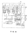
- Fig. 1 is a block diagram of a color copying machine embodying the present invention.
- a synchronization signal processing unit 1 generates various timing signals in synchronization with a horizontal synchronization signal 32 supplied from a tone control circuit 21 in response to a signal from a beam detector 20 of a printer unit 200.
- a contact-type CCD sensor block 2 reads and converts an original image into an electrical signal 5, in response to a reader horizontal synchronization signal RHSYNC and a drive signal 4 generated by the synchronization signal processing unit 1.
- a signal processing unit 3 is provided for a signal shaping in order to prevent attenuation of high-frequency components of the signal 5.
- the image signal from the signal processing unit 3 is at first supplied to an analog process unit 7.
- the image signal of each color digitized in the analog processing unit 7 is divided in 5 channels which are mutually unsynchronized.
- said channels are synthesized by a jointing memory 8 to obtain unified image data.
- the image data synthesized and converted into Y, M and C signals in the jointing memory 8 are supplied, in synchronous manner, to an image processing unit (IPU) 9 for effecting a shading correction and a masking correction.
- IPU image processing unit
- a desired color signal is selected by a control unit 10 of the reader unit 100, and an 8-bit color signal after predetermined color conversion is supplied from the IPU 9 to the printer unit 200 through a data line 11.
- control unit 10 activates a motor driver 13 to control a motor 12 for scanning the original image, and also controls a CVR unit 15 for controlling an exposure lamp 14 and an operation unit 16 for instructing copy and other operations.
- an unrepresented mode selector switch for achieving a sharp reproduction from a latter original and a tonal reproduction from a photograph original, and the information of such mode is supplied from the operation unit 16 to the control unit 10 and then to the printer unit.
- control unit of the printer controls a selector of a binary digitizing circuit to be explained later, according to the signal from a CPU 25-1.
- the image data 11 from the reader unit 100 are supplied to a tone control circuit 21 of the printer unit 200.
- the tone control circuit 21 has a function of synchronizing the image clock signal of the reader unit 100 with the image clock signal of the printer unit 200, and a function of correlating the image data with the reproduced color density in the printer unit 200.
- the output signal from the tone control circuit 21 is supplied to a laser driver 22 for driving a laser element 23, thereby effecting image formation.
- the control unit 25 of the printer communicates with the reader unit 100 through a communication control line 24 and controls various units of the printer 200.
- a potential sensor 26 for detecting the charge on a photosensitive member 29, and a potential measuring unit 27 for converting the output signal of the potential sensor 26 into a digital signal for supply to the control unit 25.
- a potential signal supplied to the control unit 25 is fetched by the CPU 25-1 thereof for use in a control operation to be explained later.
- an image top signal ITOP indicating the leading end of the image from a sensor 28 is also supplied to the control unit 25 for controlling the recording operation.
- signals from a humidity sensor 98 and a temperature sensor 99, for correcting the developing characteristics are supplied through an A/D converter 25-3 of the control unit 25.
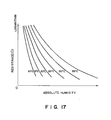
- the humidity sensor 98 in the present embodiment varies the resistance according to the relative humidity, as shown in Fig. 17, showing the resistance in ordinate and the relative humidity in abscissa.
- ⁇ H indicating the ratio of the amount of vapor in the air to the saturated amount of vapor at each temperature
- ⁇ H f(T, H)
- Said function f is generally represented by a third-order function.
- the relative humidity is determined by obtaining said T and H from the output signals of the temperature sensor 99 and the humidity sensor 98, converting said signals into digital signals by the A/D converter 25-3 of the control unit and processing thus obtained digital signals.
- the relative humidity thus determined is used in a control operation to be explained later.
- Fig. 8 is a cross-sectional view of a copying machine utilizing the contact-type CCD sensor of the present embodiment.
- the copying machine 80 is composed of a reader unit 100 and a printer unit 200.
- An original scanning unit 83 is adapted to move in a direction A for reading the image of an original document 84 placed on an original support plate, simultaneously turning on an exposure lamp 85 in the scanning unit 83.
- the light reflected from the original is guided to a converging rod lens array 86 and focused on a contact-type color CCD sensor 87, consisting of a staggered arrangement of 5 CCD chips of 1024 pixels each, wherein each pixel has a size of 62.5 ⁇ m (1/16 mm) and is divided into three areas of 15.5 ⁇ 62.5 ⁇ m each, having respectively cyan, green and yellow filters.
- the optical image focused on the color CCD sensor 87 is converted into electric signals of respective colors, which are subjected to a process to be explained later in an image processing block 88.
- the color-separated image signals released from said block 88 are supplied to the printer 200 for image printing.
- the color image signals from the reader 100 are used, after pulse width modulation etc., for driving the laser element.
- the laser beam modulated according to the image signals is deflected into a scanning motion by a polygon mirror 89 rotated at a high speed, then reflected by a mirror 90 and irradiates the surface of a photosensitive drum 91 to effect dot exposure thereon corresponding to the image.
- a horizontal scanning line of the laser beam corresponds to a horizontal scanning line of the image and has a width of 1/16 mm in the present embodiment.
- the photosensitive drum 91 As the photosensitive drum 91 is rotated in a direction indicated by an arrow at a constant speed, a two-dimensional image is exposed thereon by a main scanning achieved by the movement of said laser beam and a sub scanning achieved by said rotation of the photosensitive drum 91.
- the photosensitive drum 91 is uniformly charged in advance by a charger 97, and a latent image is formed by the exposure on said photosensitive drum.
- a latent image corresponding to the signal of a particular color is developed in one of developing units 92 - 95 corresponding to said color.
- a dot image of the yellow component of said original image is exposed on the photosensitive drum 91, and is developed by the yellow developing unit 92.
- the yellow image thus obtained is transferred onto a sheet wound on a transfer drum 96, by means of a transfer charger 98 at the contact point of the photosensitive drum 91 and the transfer drum 96, whereby a yellow toner image is formed on said sheet.
- a transfer charger 98 at the contact point of the photosensitive drum 91 and the transfer drum 96, whereby a yellow toner image is formed on said sheet.
- Same process is repeated for magenta, cyan and black colors, and these color images are superposed on said sheet to obtain a four-color toner image.
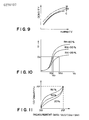
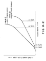
- Fig. 9 shows the image density as a function of the surface potential of the photosensitive drum, in which humidity is taken as a parameter.
- V C2 150 V
- V C1 240 V
- V C0 300 V
- the laser power is switched at the relative humidity of 50%, and is selected lower or higher respectively above or below the humidity of 50 %.
- Fig. 2 is a block diagram of the tone control circuit 21.
- the 8-bit image data 11 released from the IPU 9 of the reader 100 is supplied to a buffer memory 30 in synchronization with a synchronization signal RHSYNC and an image clock signal RCLK from the synchronization signal process unit 1, and the image signal stored in the buffer memory 30 is read therefrom in synchronization with signals HSYNC and CLK 32 from a synchronization control unit 31.
- the image signal is adjusted to the difference in synchronization and speed between the reader 100 and the printer 200, and is supplied to a selector 33.
- a selection signal 34 from a CPU 25-1 of a control unit 25 selects the input A of the selector 33
- the image signal is supplied to the address terminal of a look-up table RAM (LUTRAM) 38.
- LTRAM look-up table RAM
- the CPU 25-1 selects the reading mode of the RAM 3 by a control signal 36
- data corresponding to the address input are released from the RAM 38.
- the released data are supplied to a selector 39, and further supplied to a next selector 40 by the aforementioned selection signal 34.
- a selection signal 42 of the selector 40 selects the input A, said data are supplied to a D/A converter 41 for conversion into an analog signal.
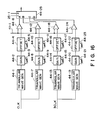
- the analog image signal 41-1 thus obtained is binary encoded by a binary encoding circuit 44, of which an example is shown in Fig. 16.
- a binary encoding circuit 44 In response to a clock signal 51 released from the synchronization control unit 31, triangular wave generators 44-1, 44-7, 44-13 and 44-19 generate triangular waves, which are subjected to the regulation of gain level and offset set by variable resistors 44-3, 44-9, 44-15, 44-21, 44-5, 44-11, 44-17 and 44-23 and are compared with the analog image signal 41-1 in comparators 44-6, 44-12, 44-18 and 44-24 to obtain pulse-width modulated signals for supply to inputs A - D of a selector 44-25.
- Fig. 14-2 shows the relation between the released pulse width and the amount of laser beam emission.
- the aforementioned variable resistors for regulating the gain and offset levels are manually regulated in cooperation with an energy measuring device provided in the optical path, in such a manner that the level 00 H corresponds to the initial position of the linear portion and the level FF H corresponds to a position immediately before the end of said linear portion.
- the laser current becomes different when the laser power is switched as will be explained later.
- the amount of light emission becomes different even with a same pulse duration as shown in Fig. 14-1. Consequently, when the laser power is varied, the linear range of the amount of light emission as a function of the pulse duration supplied to the laser driver 22 varies depending on the laser power, as indicated by curves (1) and (2) in Fig. 14-2, respectively corresponding to higher and lower laser power levels.
- plural binary encoding circuits for the switched levels of the laser power are also provided for a clock signal 3LCK 52 of a frequency different from that of the clock signal 51 from the synchronization control unit 31.
- the selector 44-25 selects one of plural pulse-width modulated binary image signals according to a signal from the CPU 25-1.
- the image signal pulse-width modulated by the binary encoding circuit 44 is supplied, through an OR gate 45 and an AND gate 46, to the laser driver 22.
- Fig. 15 shows the details of said laser driver 22, in which an analog switch 22-7 is controlled according to the information discriminated by the control unit 25, thereby varying the constant current supplied to the laser element 23, as will be explained in more detail in the following.
- the signal from the AND gate 46 of the tone control circuit 21 is supplied, through a buffer 22-1 in the laser driver 22, to a transistor 22-2 constituting a differential circuit, of which the other transistor 22-3 is used for driving the laser element 23. These transistors are given a constant current by a transistor 22-4.
- An operational amplifier 22-5 receives, at the positive input terminal thereof, a signal supplied from a constant voltage source 22-6, and, at the negative input terminal thereof, a voltage across a resistor R5 for detecting the current in the transistor 22-4, and supplies the transistor 22-4 with a voltage for causing a constant current.
- an analog switch 22-7 controlled by a buffer 22-8 receiving an I/O signal from the control unit 25, varies the voltage supplied to the positive input terminal of the operational amplifier 22-5, thereby varying the current supplied to the laser element 23.
- the analog switch 22-7 is controlled according to the humidity information, thereby switching the current to be supplied to the laser element.
- the output of the operational amplifier increases to elevate the current without limit, thereby eventually leading to the destruction of the semiconductor laser.
- the analog switch is provided for preventing such phenomenon.
- a blanking signal 48 from the synchronization control unit 31 is used for turning on the laser element 23 for enabling the beam detector to detect the arrival of the beam.
- An inhibit signal 49 from the CPU 25-1 is used for inhibiting the function of the laser element 23, thereby extending the service life thereof.
- a pattern generator 50 generates a predetermined pattern for chacking the image signal, and, it receives a transfer drum synchronization signal ITOP, the horizontal synchronization signal HSYNC of the printer 200 and a control signal from the CPU 25-1. When said pattern signal is released, the CPU 25-1 shifts the selection signal 42 for the selector 40 to the input B, thereby supplying the signal of the pattern generator 50 to the D/A converter 41 and thus checking the image signal.
- the synchronization control unit 31 releases a clock signal CLK 51 or 3LCK 52 for generating triangular wave based on a reference clock signal from a crystal oscillator in response to an instruction from the CPU 25-1. It also receives the beam detection signal from the beam detector 20, and releases the blanking signal 48, the horizontal synchronization signal HSYNC of the printer 200, and the image clock signal CLK.
- the binary encoding circuit 44 releases a binary encoded signal 47 in synchronization with the CLK signal 51 or the 3CLK signal 52.
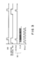
- Fig. 3 is a timing chart showing the timing of said beam detection signal and blanking signal 48.
- the synchronization control unit 31 receives a clock signal, from a crystal oscillator, of a frequency larger than twice of that of the image clock signal, and releases the signals HSYNC and CLK in synchronization with the beam detection signal and said clock signal.
- the blanking signal 48 is formed by a counter which is reset at the end of the beam detection signal BD and measures a period shorter than the period of said beam detection signal BD.
- Fig. 4 is a flow chart showing the function of the CPU 10-1 of the control unit 10 of the reader 100, and a corresponding program is stored in the ROM 10-2 shown in Fig. 1A.
- a step S1 executes an initial display routine, including the checking of input/output states, initialization of the RAM 10-3 in Fig. 1A and movement of the scanning start point. Then a step S2 detects whether the reader 100 is connected with the printer 200. A step S3 discriminates whether a print switch in the operation unit 16 has been actuated, and, if actuated, a step S4 sends a print-on command to the printer 200. Then a step S5 awaits the entry of the signal ITOP from the printer 200, and, upon entry thereof, a step S6 initiates the scanning of the original image with a designated color mode and sends the image signal to the printer 200.
- Fig. 5 is a flow chart of the control sequence of the control unit 25 of the printer 200, and a corresponding program is stored in the ROM 25-2 shown in Fig. 1B.
- a step S10 executes an initial routine, including the checking of input/output states, initialization of the RAM and removal of retentive charge on the photosensitive drum.
- a step S11 then checks the connection with the reader 100, and, when said connection is confirmed, a step S12 discriminates whether the heater of the fixing unit has been warmed up to a predetermined temperature.
- a step S13 discriminates whether a print command has been sent from the reader 100.
- a step S14 executes a process PGON to be explained later, respectively for the clock signals used for generating the triangular wave and for controlling the laser power.
- a step S15 calculates the data to be stored in the LUTRAM 38 according to the humidity data and the character/photograph information (data for selecting the clock signal CLK or 3CLK) from the reader, based on the result of the step S14 as will be explained later.
- the clock signal CLK or 3CLK is selected respectively for the character information or the photograph information.
- the calculated data are stored in the LUTRAM 38 in a step S16, by selecting the input terminal B of the selector 33 by the selection signal 34 and connecting a data bus 36 of the CPU 25-1 through the selector 39 to the data input terminal of the LUTRAM 38.
- the CPU 25-1 releases the address of the LUTRAM 38 to an address bus 35 and the data to be stored to a data but 37, and the storage into the LUTRAM 38 is conducted by the entry of writing pulses in response to the control signal 36.
- a step S17 discriminates whether the storage in the LUTRAM 38 has been completed, and, if completed, a step S18 sends the signal ITOP to the reader 100.
- the sequence proceeds from the step S5 to S6.
- a step S19 sets a designated color mode, and the tone control is executed by switching the address of the LUTRAM 38 for each color.
- a step S20 executes a printing operation of the designated color. Upon completion of a designation color mode of color image formation, the sequence returns to the step S11.
- the PGON processes in the steps S14-1 to S14-4 are summarized in Fig. 6 as they are mutually same except for the laser power and the clock signal used for generating the triangular wave.
- Fig. 6 is a flow chart of the PGON process in the step S14 in Fig. 5, for activating the pattern generator 50 to release a predetermined pattern and reading the surface potential of the photosensitive drum.
- a step S30 causes the selection signal 42 to select the input terminal B of the selector 40, for supplying the signal of the pattern generator 50 to the D/A converter 41.
- a step S31 causes the potential measuring unit 27 to measure the potential which is generated on the photosensitive drum 29 by a laser beam emitted in response to a signal, for example "00", from the pattern generator 50.
- the binary digitizing circuit 44 is so adjusted in advance that the comparators 44-6, 44-12, 44-18 and 44-24 release a limit pulse enough for inducing light emission from the laser element in response to a "0" input signal to the D/A converter 41.
- the photosensitive member 29 is uniformly irradiated by the laser driver 22 and laser element 23.
- the binary encoding circuit 44 is so adjusted in advance that the laser element 23 emits light with a period shorter than the period of the triangular wave, thereby exactly reproducing dots when the pattern generator 50 releases a hexadecimal signal "FF" in the step S31, and the potential corresponding to said signal "FF" is read in the same manner.
- a step S32 determines the target surface potential V C0 from Fig. 10 in order to provide a predetermined image density in response to the detected humidity, and discriminates whether the difference of the measured potentials V00 and V FF respectively corresponding to the signals "00" and "FF" from the pattern generator 50 is equal to a predetermined value. If not, the sequence proceeds to a step S33 for varying the high voltage of the charger 97 shown in Fig. 1, and the sequence returns to the step S31 for repeating the procedure.
- step S34 for activating the pattern generator 50, whereupon the pattern generator 50 starts to function as a m-bit counter for counting the HSYNC signal in synchronization with the ITOP signal, and releases signals in succession, by dividing the signals "00" to "FF" into a predetermined number m of levels.
- the signal thus obtained is supplied through the selector 40 to the D/A converter 41 for obtaining an analog signal for driving the laser element 23.
- Steps 35 and 36 read the potential of the photosensitive member 29 varying in m levels in response to said analog signal, and store said potential in succession corresponding to the output signal of the pattern generator 50.
- said number m is taken as 16.
- Fig. 7 shows the relation between the input signal of the D/A converter 41 and the voltage measured by the potential measuring unit 27.
- the photosensitive member 29 is charged to a negative potential, so that the potential is elevated by the irradiation with a laser beam, and negatively charged toner is correspondingly deposited.
- V DD indicates a charge level when the laser is not activated
- V L indicates a charge level when the laser is fully activated.
- the PGON process is executed, prior to every copying sequence, for all the laser power levels and the clock signal for generating the triangular wave, but said process may be conducted at a predetermined interval with a suitable timer, or after a predetermined number of copying operations. Also it may be conducted for a selected laser power level and a selected clock signal.
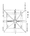
- Fig. 12 shows the relationship between the input image signal and the output image density wherein;
- the VD curve is selected from plural curves stored in advance in the ROM 25-2 according to the developers, laser power levels and the clock signals for generating triangular wave for use in the binary encoding circuit 44 in Fig. 2 (clock signals CLK 51, 3CLK 52).
- the PG process for potential measurement (step S34 in Fig. 6) is conducted by storing a table corresponding to the selected VD-curve (table with inverted x- and y-axes of the VD-curve) in the LUTRAM 38, and utilizing the data converted by the table in the LUTRAM 38. Said data stored in the LUTRAM 38 may also be stored in advance in a ROM.
- the preparation of the look-up table is conducted in such a manner that a conversion level Ei is obtained corresponding to the input level ei and the density level Di, in order that the output density D varies linearly as a function of the input level e, wherein the output ei of the pattern generator provides a measured potential Vi corresponding to a density Di according to the VD curve.
- the output of the pattern generator is varied in 16 levels in the present embodiment, there are prepared 16 LUT data, and said data are completed from "00" to "FF" by approximation with folded lines.
- the look-up table is formed in a RAM, but it is also possible to store plural data groups in a ROM and to select a suitable group according to the result of calculation by the CPU.
- the foregoing embodiment allows to obtain stable image by maintaining a constant relationship between the potential on the photosensitive member and the image signal and also taking the characteristic of developer into cinsideration. Also in case of a color image, it allows to prevent fluctuation in colors, thereby providing an image with constant color.
Landscapes
- Engineering & Computer Science (AREA)
- Physics & Mathematics (AREA)
- Signal Processing (AREA)
- Multimedia (AREA)
- General Physics & Mathematics (AREA)
- Optics & Photonics (AREA)
- Microelectronics & Electronic Packaging (AREA)
- Plasma & Fusion (AREA)
- Color, Gradation (AREA)
- Facsimile Image Signal Circuits (AREA)
- Control Or Security For Electrophotography (AREA)
- Color Electrophotography (AREA)
- Exposure Or Original Feeding In Electrophotography (AREA)
Priority Applications (1)
| Application Number | Priority Date | Filing Date | Title |
|---|---|---|---|
| EP93202855A EP0589539B1 (fr) | 1987-01-19 | 1988-01-18 | Appareil de formation d'images |
Applications Claiming Priority (10)
| Application Number | Priority Date | Filing Date | Title |
|---|---|---|---|
| JP9463/87 | 1987-01-19 | ||
| JP9462/87 | 1987-01-19 | ||
| JP9461/87 | 1987-01-19 | ||
| JP62009462A JPH0795200B2 (ja) | 1987-01-19 | 1987-01-19 | 画像形成装置 |
| JP9465/87 | 1987-01-19 | ||
| JP62009464A JP2810365B2 (ja) | 1987-01-19 | 1987-01-19 | 画像形成装置 |
| JP62009463A JPH0795201B2 (ja) | 1987-01-19 | 1987-01-19 | 画像形成装置 |
| JP62009465A JPS63177158A (ja) | 1987-01-19 | 1987-01-19 | 画像形成装置 |
| JP62009461A JP2632826B2 (ja) | 1987-01-19 | 1987-01-19 | 画像形成装置 |
| JP9464/87 | 1987-01-19 |
Related Child Applications (2)
| Application Number | Title | Priority Date | Filing Date |
|---|---|---|---|
| EP93202855.8 Division-Into | 1988-01-18 | ||
| EP93202855A Division EP0589539B1 (fr) | 1987-01-19 | 1988-01-18 | Appareil de formation d'images |
Publications (2)
| Publication Number | Publication Date |
|---|---|
| EP0276107A2 true EP0276107A2 (fr) | 1988-07-27 |
| EP0276107A3 EP0276107A3 (fr) | 1990-03-28 |
Family
ID=27519067
Family Applications (2)
| Application Number | Title | Priority Date | Filing Date |
|---|---|---|---|
| EP93202855A Expired - Lifetime EP0589539B1 (fr) | 1987-01-19 | 1988-01-18 | Appareil de formation d'images |
| EP88300360A Withdrawn EP0276107A3 (fr) | 1987-01-19 | 1988-01-18 | Appareil de formation d'images |
Family Applications Before (1)
| Application Number | Title | Priority Date | Filing Date |
|---|---|---|---|
| EP93202855A Expired - Lifetime EP0589539B1 (fr) | 1987-01-19 | 1988-01-18 | Appareil de formation d'images |
Country Status (3)
| Country | Link |
|---|---|
| US (2) | US4989039A (fr) |
| EP (2) | EP0589539B1 (fr) |
| DE (1) | DE3856525T2 (fr) |
Cited By (15)
| Publication number | Priority date | Publication date | Assignee | Title |
|---|---|---|---|---|
| EP0368617A2 (fr) * | 1988-11-08 | 1990-05-16 | Canon Kabushiki Kaisha | Appareil de formation d'images avec des moyens de contrôle de l'attraction électrostatique de matière de transfert |
| EP0415754A1 (fr) * | 1989-08-31 | 1991-03-06 | Canon Kabushiki Kaisha | Un appareil de formation d'images |
| EP0425698A1 (fr) * | 1989-05-10 | 1991-05-08 | Canon Kabushiki Kaisha | Appareil de formation d'images |
| EP0426435A2 (fr) * | 1989-10-31 | 1991-05-08 | Canon Kabushiki Kaisha | Dispositif de formation d'images pour la reproduction de demi-teintes |
| EP0434416A2 (fr) * | 1989-12-20 | 1991-06-26 | Xerox Corporation | Appareil d'impression électrographique |
| EP0526238A2 (fr) * | 1991-08-01 | 1993-02-03 | Canon Kabushiki Kaisha | Appareil à couleurs électrophotographique |
| US5276483A (en) * | 1988-11-08 | 1994-01-04 | Canon Kabushiki Kaisha | Image forming apparatus provided with an attraction charger controlled by one or more ambient conditions |
| US5283658A (en) * | 1989-05-10 | 1994-02-01 | Canon Kabushiki Kaisha | Image forming apparatus with TTL to ECL conversion between reading and printing circuits |
| EP0590884A2 (fr) * | 1992-09-28 | 1994-04-06 | Canon Kabushiki Kaisha | Méthode et appareil de formation d'images |
| EP0628887A3 (fr) * | 1991-02-22 | 1995-07-19 | Canon Kk | Appareil de formation d'images. |
| EP0770929A3 (fr) * | 1995-10-27 | 1997-05-21 | Canon Kabushiki Kaisha | Appareil de formation d'images |
| EP0819991A1 (fr) * | 1996-07-18 | 1998-01-21 | Agfa-Gevaert N.V. | Procédé de commande d'un dispositif électrophotographique |
| WO1999030482A1 (fr) * | 1997-12-09 | 1999-06-17 | Heidelberger Druckmaschinen Aktiengesellschaft | Procede de fonctionnement d'un organe de gravure |
| US5974279A (en) * | 1996-07-18 | 1999-10-26 | Agfa Gevaert N.V. | Process control of electrophotographic device |
| WO2005114803A2 (fr) * | 2004-05-19 | 2005-12-01 | Intense Limited | Impression avec activation laser |
Families Citing this family (25)
| Publication number | Priority date | Publication date | Assignee | Title |
|---|---|---|---|---|
| EP0388833B1 (fr) * | 1989-03-20 | 1996-06-19 | Hitachi, Ltd. | Système d'enregistrement optique |
| JPH0353266A (ja) * | 1989-07-21 | 1991-03-07 | Canon Inc | 画像形成装置 |
| JPH0387859A (ja) * | 1989-08-31 | 1991-04-12 | Canon Inc | 画像形成装置 |
| US5719613A (en) * | 1990-03-20 | 1998-02-17 | Minolta Co., Ltd. | Apparatus for forming an image with use of electrophotographic process |
| US5959650A (en) * | 1990-03-20 | 1999-09-28 | Minolta Co., Ltd. | Apparatus for forming an image with use of electrophotographic process |
| JP3018395B2 (ja) * | 1990-05-15 | 2000-03-13 | ミノルタ株式会社 | 画像形成装置のトナー濃度制御装置 |
| JP3006622B2 (ja) * | 1990-05-15 | 2000-02-07 | ミノルタ株式会社 | 画像形成装置 |
| JPH0434563A (ja) * | 1990-05-31 | 1992-02-05 | Toshiba Corp | 画像形成装置 |
| JPH0463367A (ja) * | 1990-07-03 | 1992-02-28 | Toshiba Corp | 画像形成装置 |
| US5453773A (en) * | 1990-11-30 | 1995-09-26 | Minolta Camera Kabushiki Kaisha | Electrophotographic image forming apparatus comprising means for automatically adjusting image reproduction density |
| JP2562087Y2 (ja) * | 1991-03-15 | 1998-02-04 | 旭光学工業株式会社 | レーザーパワー調整装置 |
| EP0506483B1 (fr) * | 1991-03-29 | 1999-02-17 | Canon Kabushiki Kaisha | Appareil pour enregistrer de l'information et méthode d'enregistrement d'images |
| KR960006814B1 (ko) * | 1993-05-31 | 1996-05-23 | 삼성전자주식회사 | 전자사진 방식 프린터의 광신호 제어방법 및 장치 |
| JPH0758958A (ja) * | 1993-07-01 | 1995-03-03 | Xerox Corp | グレイ画素ハーフトーンシステム及びカラー印刷におけるトナーデポジションの制御 |
| US7031020B1 (en) * | 1994-04-22 | 2006-04-18 | Canon Kabushiki Kaisha | Image processing method, apparatus and controller |
| JP3282404B2 (ja) * | 1994-09-26 | 2002-05-13 | ミノルタ株式会社 | 画像形成装置 |
| JPH08156329A (ja) * | 1994-12-12 | 1996-06-18 | Fuji Xerox Co Ltd | 画像形成装置 |
| US5748225A (en) * | 1995-03-31 | 1998-05-05 | Agfa Division, Bayer Corporation | Condition sensitive method and apparatus for imaging a lithographic printing plate |
| JPH08290608A (ja) * | 1995-04-24 | 1996-11-05 | Minolta Co Ltd | 画像形成装置 |
| JP3658055B2 (ja) * | 1995-10-12 | 2005-06-08 | キヤノン株式会社 | 画像形成装置の電源制御装置 |
| US6127939A (en) | 1996-10-14 | 2000-10-03 | Vehicle Enhancement Systems, Inc. | Systems and methods for monitoring and controlling tractor/trailer vehicle systems |
| JPH10133436A (ja) * | 1996-10-25 | 1998-05-22 | Mita Ind Co Ltd | 画像形成装置 |
| JP3978836B2 (ja) * | 1997-12-17 | 2007-09-19 | ブラザー工業株式会社 | 画像記録装置 |
| JP3595745B2 (ja) * | 1999-01-29 | 2004-12-02 | キヤノン株式会社 | 画像処理装置 |
| JP2001096794A (ja) * | 1999-09-29 | 2001-04-10 | Fuji Xerox Co Ltd | 走査露光装置、半導体レーザ駆動回路、画像形成装置 |
Citations (4)
| Publication number | Priority date | Publication date | Assignee | Title |
|---|---|---|---|---|
| US4122409A (en) * | 1976-03-10 | 1978-10-24 | Xerox Corporation | Method and apparatus for controlling the intensity of a laser output beam |
| DE3409406A1 (de) * | 1983-03-15 | 1984-09-20 | Canon K.K., Tokio/Tokyo | Bildreproduktionsgeraet |
| DE3512060A1 (de) * | 1984-04-02 | 1985-10-03 | Canon K.K., Tokio/Tokyo | Bilderzeugungsgeraet |
| JPS61132964A (ja) * | 1984-12-03 | 1986-06-20 | Canon Inc | 画像形成装置 |
Family Cites Families (19)
| Publication number | Priority date | Publication date | Assignee | Title |
|---|---|---|---|---|
| US2357809A (en) * | 1940-11-16 | 1944-09-12 | Chester F Carlson | Electrophotographic apparatus |
| US3649114A (en) * | 1969-05-14 | 1972-03-14 | Xerox Corp | Multiple output electrostatic recording system |
| US4105321A (en) * | 1976-10-27 | 1978-08-08 | Xerox Corporation | Illuminated charge control system for xerographic machines |
| JPS55117164A (en) * | 1979-03-02 | 1980-09-09 | Canon Inc | Image forming device |
| JPS5627177A (en) * | 1979-08-14 | 1981-03-16 | Toshiba Corp | Copying unit |
| JPS5686776A (en) * | 1979-12-18 | 1981-07-14 | Ricoh Co Ltd | Information write-in method |
| JPS5865450A (ja) * | 1981-10-15 | 1983-04-19 | Canon Inc | 電子写真方法 |
| DE3408336A1 (de) * | 1983-03-08 | 1984-09-13 | Canon K.K., Tokio/Tokyo | Bildreproduktionssystem |
| US4646249A (en) * | 1983-06-16 | 1987-02-24 | Canon Kabushiki Kaisha | Image processing system |
| US4680646A (en) * | 1983-09-05 | 1987-07-14 | Canon Kabushiki Kaisha | Image forming device for reproducing a half-tone image |
| JPS61114647A (ja) * | 1984-11-09 | 1986-06-02 | Sharp Corp | 画像読取装置 |
| JPH0824340B2 (ja) * | 1984-11-15 | 1996-03-06 | キヤノン株式会社 | 画像信号処理装置 |
| US4709250A (en) * | 1985-02-19 | 1987-11-24 | Canon Kabushiki Kaisha | Image forming apparatus |
| JPS61284171A (ja) * | 1985-06-11 | 1986-12-15 | Canon Inc | レ−ザ−ビ−ムプリンタ |
| US4870499A (en) * | 1985-08-29 | 1989-09-26 | Canon Kabushiki Kaisha | Image processing apparatus |
| US4782398A (en) * | 1986-02-14 | 1988-11-01 | Canon Kabushiki Kaisha | Image processing apparatus |
| JP2556486B2 (ja) * | 1986-11-14 | 1996-11-20 | キヤノン株式会社 | フィルム読取装置 |
| JP2607490B2 (ja) * | 1986-12-09 | 1997-05-07 | キヤノン株式会社 | 画像形成装置の画質制御方法 |
| JPH06150425A (ja) * | 1992-11-06 | 1994-05-31 | Olympus Optical Co Ltd | 光ピックアップ |
-
1988
- 1988-01-14 US US07/144,047 patent/US4989039A/en not_active Expired - Lifetime
- 1988-01-18 EP EP93202855A patent/EP0589539B1/fr not_active Expired - Lifetime
- 1988-01-18 DE DE3856525T patent/DE3856525T2/de not_active Expired - Fee Related
- 1988-01-18 EP EP88300360A patent/EP0276107A3/fr not_active Withdrawn
-
1995
- 1995-03-13 US US08/402,987 patent/US5473415A/en not_active Expired - Lifetime
Patent Citations (4)
| Publication number | Priority date | Publication date | Assignee | Title |
|---|---|---|---|---|
| US4122409A (en) * | 1976-03-10 | 1978-10-24 | Xerox Corporation | Method and apparatus for controlling the intensity of a laser output beam |
| DE3409406A1 (de) * | 1983-03-15 | 1984-09-20 | Canon K.K., Tokio/Tokyo | Bildreproduktionsgeraet |
| DE3512060A1 (de) * | 1984-04-02 | 1985-10-03 | Canon K.K., Tokio/Tokyo | Bilderzeugungsgeraet |
| JPS61132964A (ja) * | 1984-12-03 | 1986-06-20 | Canon Inc | 画像形成装置 |
Non-Patent Citations (1)
| Title |
|---|
| PATENT ABSTRACTS OF JAPAN, Vol. 10, No. 327 (P-513)(2383), November 7, 1986; & JP-A-61 132 964 (CANON INC.) 20-06-1986 * |
Cited By (30)
| Publication number | Priority date | Publication date | Assignee | Title |
|---|---|---|---|---|
| EP0368617A3 (en) * | 1988-11-08 | 1990-11-28 | Canon Kabushiki Kaisha | Image forming apparatus having electrostatic attraction control means for transfer material |
| EP0368617A2 (fr) * | 1988-11-08 | 1990-05-16 | Canon Kabushiki Kaisha | Appareil de formation d'images avec des moyens de contrôle de l'attraction électrostatique de matière de transfert |
| US5276483A (en) * | 1988-11-08 | 1994-01-04 | Canon Kabushiki Kaisha | Image forming apparatus provided with an attraction charger controlled by one or more ambient conditions |
| EP0425698A4 (en) * | 1989-05-10 | 1993-03-31 | Canon Kabushiki Kaisha | Image forming apparatus |
| EP0425698A1 (fr) * | 1989-05-10 | 1991-05-08 | Canon Kabushiki Kaisha | Appareil de formation d'images |
| US5283658A (en) * | 1989-05-10 | 1994-02-01 | Canon Kabushiki Kaisha | Image forming apparatus with TTL to ECL conversion between reading and printing circuits |
| EP0415754A1 (fr) * | 1989-08-31 | 1991-03-06 | Canon Kabushiki Kaisha | Un appareil de formation d'images |
| US5313308A (en) * | 1989-08-31 | 1994-05-17 | Canon Kabushiki Kaisha | Image forming apparatus which changes its tone reproducing property in accordance with ambient conditions |
| EP0426435A2 (fr) * | 1989-10-31 | 1991-05-08 | Canon Kabushiki Kaisha | Dispositif de formation d'images pour la reproduction de demi-teintes |
| US5565995A (en) * | 1989-10-31 | 1996-10-15 | Canon Kabushiki Kaisha | System for correcting a pulse-width-modulated signal in a recording apparatus |
| US5463473A (en) * | 1989-10-31 | 1995-10-31 | Canon Kabushiki Kaisha | Siphen for correcting a pulse-width modulated signal in a recording apparatus |
| EP0426435B1 (fr) * | 1989-10-31 | 1997-01-15 | Canon Kabushiki Kaisha | Dispositif de formation d'images pour la reproduction de demi-teintes |
| EP0434416A3 (en) * | 1989-12-20 | 1992-02-19 | Xerox Corporation | Electrographic plotters |
| EP0434416A2 (fr) * | 1989-12-20 | 1991-06-26 | Xerox Corporation | Appareil d'impression électrographique |
| US5752126A (en) * | 1991-02-22 | 1998-05-12 | Canon Kabushiki Kaisha | Image forming apparatus |
| EP0628887A3 (fr) * | 1991-02-22 | 1995-07-19 | Canon Kk | Appareil de formation d'images. |
| EP0526238A3 (en) * | 1991-08-01 | 1993-08-11 | Canon Kabushiki Kaisha | A color electrophotographic apparatus |
| EP0526238A2 (fr) * | 1991-08-01 | 1993-02-03 | Canon Kabushiki Kaisha | Appareil à couleurs électrophotographique |
| EP0590884A3 (en) * | 1992-09-28 | 1994-07-20 | Canon Kk | Image forming method and apparatus |
| US5557412A (en) * | 1992-09-28 | 1996-09-17 | Canon Kabushiki Kaisha | Image forming method and apparatus for counterfeit protection using image synthesis accounting for forming conditions |
| US5696594A (en) * | 1992-09-28 | 1997-12-09 | Canon Kabushiki Kaisha | Image forming method and apparatus for counterfeit protection controlling image synthesis in response to forming conditions |
| EP0590884A2 (fr) * | 1992-09-28 | 1994-04-06 | Canon Kabushiki Kaisha | Méthode et appareil de formation d'images |
| EP0770929A3 (fr) * | 1995-10-27 | 1997-05-21 | Canon Kabushiki Kaisha | Appareil de formation d'images |
| US5726759A (en) * | 1995-10-27 | 1998-03-10 | Canon Kabushiki Kaisha | Image forming apparatus |
| EP0819991A1 (fr) * | 1996-07-18 | 1998-01-21 | Agfa-Gevaert N.V. | Procédé de commande d'un dispositif électrophotographique |
| US5974279A (en) * | 1996-07-18 | 1999-10-26 | Agfa Gevaert N.V. | Process control of electrophotographic device |
| WO1999030482A1 (fr) * | 1997-12-09 | 1999-06-17 | Heidelberger Druckmaschinen Aktiengesellschaft | Procede de fonctionnement d'un organe de gravure |
| US6747750B1 (en) | 1997-12-09 | 2004-06-08 | Hell Gravure Systems Gmbh | Method for operating an engraving member |
| WO2005114803A2 (fr) * | 2004-05-19 | 2005-12-01 | Intense Limited | Impression avec activation laser |
| WO2005114803A3 (fr) * | 2004-05-19 | 2006-06-01 | Intense Ltd | Impression avec activation laser |
Also Published As
| Publication number | Publication date |
|---|---|
| DE3856525D1 (de) | 2002-05-16 |
| EP0589539A1 (fr) | 1994-03-30 |
| EP0589539B1 (fr) | 2002-04-10 |
| US4989039A (en) | 1991-01-29 |
| US5473415A (en) | 1995-12-05 |
| EP0276107A3 (fr) | 1990-03-28 |
| DE3856525T2 (de) | 2002-09-12 |
Similar Documents
| Publication | Publication Date | Title |
|---|---|---|
| US5473415A (en) | Image forming apparatus having a converter for image data characteristics | |
| US5153609A (en) | Image forming apparatus | |
| US5274424A (en) | Image forming apparatus controlled according to smallest non-zero toner density | |
| US5077605A (en) | Color image reading apparatus having shading correction for plural color component signals | |
| US6320605B1 (en) | Image information processing apparatus and method | |
| US5212560A (en) | Electrophotographic image forming apparatus comprising means for automatically adjusting image reproduction density | |
| JPH04337763A (ja) | 画像形成装置 | |
| US5453773A (en) | Electrophotographic image forming apparatus comprising means for automatically adjusting image reproduction density | |
| JP2510548B2 (ja) | 画像形成装置 | |
| JP2810365B2 (ja) | 画像形成装置 | |
| JP3013441B2 (ja) | デジタル画像形成装置 | |
| JP2872271B2 (ja) | 画像形成装置 | |
| US6538683B2 (en) | Image forming apparatus and a control method of an image forming apparatus | |
| JPS6331355A (ja) | 複写装置 | |
| US5467195A (en) | Density adjustment in an image processing apparatus | |
| JP2738413B2 (ja) | 画像処理方法 | |
| JP4058138B2 (ja) | 画像処理装置及び画像処理方法 | |
| JP3190269B2 (ja) | 画像処理方法 | |
| JPS63177158A (ja) | 画像形成装置 | |
| JP2889542B2 (ja) | 画像処理方法 | |
| JPH09172545A (ja) | 画像形成方法とその画像形成装置 | |
| JPS63177156A (ja) | 画像形成装置 | |
| JP2721358B2 (ja) | 画像形成装置 | |
| JPH0795201B2 (ja) | 画像形成装置 | |
| JPH0511552A (ja) | デジタル画像形成装置 |
Legal Events
| Date | Code | Title | Description |
|---|---|---|---|
| PUAI | Public reference made under article 153(3) epc to a published international application that has entered the european phase |
Free format text: ORIGINAL CODE: 0009012 |
|
| AK | Designated contracting states |
Kind code of ref document: A2 Designated state(s): DE FR GB IT NL |
|
| PUAL | Search report despatched |
Free format text: ORIGINAL CODE: 0009013 |
|
| AK | Designated contracting states |
Kind code of ref document: A3 Designated state(s): DE FR GB IT NL |
|
| 17P | Request for examination filed |
Effective date: 19900814 |
|
| 17Q | First examination report despatched |
Effective date: 19920626 |
|
| STAA | Information on the status of an ep patent application or granted ep patent |
Free format text: STATUS: THE APPLICATION IS DEEMED TO BE WITHDRAWN |
|
| 18D | Application deemed to be withdrawn |
Effective date: 19931221 |