CN1531139A - 有源智能天线系统及其制造方法 - Google Patents
有源智能天线系统及其制造方法 Download PDFInfo
- Publication number
- CN1531139A CN1531139A CNA2004100089280A CN200410008928A CN1531139A CN 1531139 A CN1531139 A CN 1531139A CN A2004100089280 A CNA2004100089280 A CN A2004100089280A CN 200410008928 A CN200410008928 A CN 200410008928A CN 1531139 A CN1531139 A CN 1531139A
- Authority
- CN
- China
- Prior art keywords
- antenna system
- active antenna
- high resistant
- electronic switch
- signal electrode
- Prior art date
- Legal status (The legal status is an assumption and is not a legal conclusion. Google has not performed a legal analysis and makes no representation as to the accuracy of the status listed.)
- Pending
Links
Images


Classifications
-
- H—ELECTRICITY
- H01—ELECTRIC ELEMENTS
- H01Q—ANTENNAS, i.e. RADIO AERIALS
- H01Q1/00—Details of, or arrangements associated with, antennas
- H01Q1/36—Structural form of radiating elements, e.g. cone, spiral, umbrella; Particular materials used therewith
- H01Q1/38—Structural form of radiating elements, e.g. cone, spiral, umbrella; Particular materials used therewith formed by a conductive layer on an insulating support
-
- H—ELECTRICITY
- H01—ELECTRIC ELEMENTS
- H01Q—ANTENNAS, i.e. RADIO AERIALS
- H01Q21/00—Antenna arrays or systems
-
- H—ELECTRICITY
- H01—ELECTRIC ELEMENTS
- H01Q—ANTENNAS, i.e. RADIO AERIALS
- H01Q23/00—Antennas with active circuits or circuit elements integrated within them or attached to them
-
- H—ELECTRICITY
- H01—ELECTRIC ELEMENTS
- H01L—SEMICONDUCTOR DEVICES NOT COVERED BY CLASS H10
- H01L2224/00—Indexing scheme for arrangements for connecting or disconnecting semiconductor or solid-state bodies and methods related thereto as covered by H01L24/00
- H01L2224/01—Means for bonding being attached to, or being formed on, the surface to be connected, e.g. chip-to-package, die-attach, "first-level" interconnects; Manufacturing methods related thereto
- H01L2224/02—Bonding areas; Manufacturing methods related thereto
- H01L2224/04—Structure, shape, material or disposition of the bonding areas prior to the connecting process
- H01L2224/05—Structure, shape, material or disposition of the bonding areas prior to the connecting process of an individual bonding area
- H01L2224/0554—External layer
- H01L2224/0556—Disposition
- H01L2224/05568—Disposition the whole external layer protruding from the surface
-
- H—ELECTRICITY
- H01—ELECTRIC ELEMENTS
- H01L—SEMICONDUCTOR DEVICES NOT COVERED BY CLASS H10
- H01L2224/00—Indexing scheme for arrangements for connecting or disconnecting semiconductor or solid-state bodies and methods related thereto as covered by H01L24/00
- H01L2224/01—Means for bonding being attached to, or being formed on, the surface to be connected, e.g. chip-to-package, die-attach, "first-level" interconnects; Manufacturing methods related thereto
- H01L2224/02—Bonding areas; Manufacturing methods related thereto
- H01L2224/04—Structure, shape, material or disposition of the bonding areas prior to the connecting process
- H01L2224/05—Structure, shape, material or disposition of the bonding areas prior to the connecting process of an individual bonding area
- H01L2224/0554—External layer
- H01L2224/05573—Single external layer
-
- H—ELECTRICITY
- H01—ELECTRIC ELEMENTS
- H01L—SEMICONDUCTOR DEVICES NOT COVERED BY CLASS H10
- H01L2224/00—Indexing scheme for arrangements for connecting or disconnecting semiconductor or solid-state bodies and methods related thereto as covered by H01L24/00
- H01L2224/01—Means for bonding being attached to, or being formed on, the surface to be connected, e.g. chip-to-package, die-attach, "first-level" interconnects; Manufacturing methods related thereto
- H01L2224/10—Bump connectors; Manufacturing methods related thereto
- H01L2224/15—Structure, shape, material or disposition of the bump connectors after the connecting process
- H01L2224/16—Structure, shape, material or disposition of the bump connectors after the connecting process of an individual bump connector
- H01L2224/161—Disposition
- H01L2224/16151—Disposition the bump connector connecting between a semiconductor or solid-state body and an item not being a semiconductor or solid-state body, e.g. chip-to-substrate, chip-to-passive
- H01L2224/16221—Disposition the bump connector connecting between a semiconductor or solid-state body and an item not being a semiconductor or solid-state body, e.g. chip-to-substrate, chip-to-passive the body and the item being stacked
- H01L2224/16225—Disposition the bump connector connecting between a semiconductor or solid-state body and an item not being a semiconductor or solid-state body, e.g. chip-to-substrate, chip-to-passive the body and the item being stacked the item being non-metallic, e.g. insulating substrate with or without metallisation
-
- H—ELECTRICITY
- H01—ELECTRIC ELEMENTS
- H01L—SEMICONDUCTOR DEVICES NOT COVERED BY CLASS H10
- H01L2224/00—Indexing scheme for arrangements for connecting or disconnecting semiconductor or solid-state bodies and methods related thereto as covered by H01L24/00
- H01L2224/01—Means for bonding being attached to, or being formed on, the surface to be connected, e.g. chip-to-package, die-attach, "first-level" interconnects; Manufacturing methods related thereto
- H01L2224/26—Layer connectors, e.g. plate connectors, solder or adhesive layers; Manufacturing methods related thereto
- H01L2224/31—Structure, shape, material or disposition of the layer connectors after the connecting process
- H01L2224/32—Structure, shape, material or disposition of the layer connectors after the connecting process of an individual layer connector
- H01L2224/321—Disposition
- H01L2224/32151—Disposition the layer connector connecting between a semiconductor or solid-state body and an item not being a semiconductor or solid-state body, e.g. chip-to-substrate, chip-to-passive
- H01L2224/32221—Disposition the layer connector connecting between a semiconductor or solid-state body and an item not being a semiconductor or solid-state body, e.g. chip-to-substrate, chip-to-passive the body and the item being stacked
- H01L2224/32225—Disposition the layer connector connecting between a semiconductor or solid-state body and an item not being a semiconductor or solid-state body, e.g. chip-to-substrate, chip-to-passive the body and the item being stacked the item being non-metallic, e.g. insulating substrate with or without metallisation
-
- H—ELECTRICITY
- H01—ELECTRIC ELEMENTS
- H01L—SEMICONDUCTOR DEVICES NOT COVERED BY CLASS H10
- H01L2224/00—Indexing scheme for arrangements for connecting or disconnecting semiconductor or solid-state bodies and methods related thereto as covered by H01L24/00
- H01L2224/01—Means for bonding being attached to, or being formed on, the surface to be connected, e.g. chip-to-package, die-attach, "first-level" interconnects; Manufacturing methods related thereto
- H01L2224/42—Wire connectors; Manufacturing methods related thereto
- H01L2224/47—Structure, shape, material or disposition of the wire connectors after the connecting process
- H01L2224/48—Structure, shape, material or disposition of the wire connectors after the connecting process of an individual wire connector
- H01L2224/4805—Shape
- H01L2224/4809—Loop shape
- H01L2224/48091—Arched
-
- H—ELECTRICITY
- H01—ELECTRIC ELEMENTS
- H01L—SEMICONDUCTOR DEVICES NOT COVERED BY CLASS H10
- H01L2224/00—Indexing scheme for arrangements for connecting or disconnecting semiconductor or solid-state bodies and methods related thereto as covered by H01L24/00
- H01L2224/01—Means for bonding being attached to, or being formed on, the surface to be connected, e.g. chip-to-package, die-attach, "first-level" interconnects; Manufacturing methods related thereto
- H01L2224/42—Wire connectors; Manufacturing methods related thereto
- H01L2224/47—Structure, shape, material or disposition of the wire connectors after the connecting process
- H01L2224/48—Structure, shape, material or disposition of the wire connectors after the connecting process of an individual wire connector
- H01L2224/481—Disposition
- H01L2224/48151—Connecting between a semiconductor or solid-state body and an item not being a semiconductor or solid-state body, e.g. chip-to-substrate, chip-to-passive
- H01L2224/48221—Connecting between a semiconductor or solid-state body and an item not being a semiconductor or solid-state body, e.g. chip-to-substrate, chip-to-passive the body and the item being stacked
- H01L2224/48225—Connecting between a semiconductor or solid-state body and an item not being a semiconductor or solid-state body, e.g. chip-to-substrate, chip-to-passive the body and the item being stacked the item being non-metallic, e.g. insulating substrate with or without metallisation
- H01L2224/48227—Connecting between a semiconductor or solid-state body and an item not being a semiconductor or solid-state body, e.g. chip-to-substrate, chip-to-passive the body and the item being stacked the item being non-metallic, e.g. insulating substrate with or without metallisation connecting the wire to a bond pad of the item
-
- H—ELECTRICITY
- H01—ELECTRIC ELEMENTS
- H01L—SEMICONDUCTOR DEVICES NOT COVERED BY CLASS H10
- H01L2224/00—Indexing scheme for arrangements for connecting or disconnecting semiconductor or solid-state bodies and methods related thereto as covered by H01L24/00
- H01L2224/73—Means for bonding being of different types provided for in two or more of groups H01L2224/10, H01L2224/18, H01L2224/26, H01L2224/34, H01L2224/42, H01L2224/50, H01L2224/63, H01L2224/71
- H01L2224/732—Location after the connecting process
- H01L2224/73251—Location after the connecting process on different surfaces
- H01L2224/73265—Layer and wire connectors
-
- H—ELECTRICITY
- H01—ELECTRIC ELEMENTS
- H01L—SEMICONDUCTOR DEVICES NOT COVERED BY CLASS H10
- H01L2924/00—Indexing scheme for arrangements or methods for connecting or disconnecting semiconductor or solid-state bodies as covered by H01L24/00
- H01L2924/0001—Technical content checked by a classifier
- H01L2924/00014—Technical content checked by a classifier the subject-matter covered by the group, the symbol of which is combined with the symbol of this group, being disclosed without further technical details
Landscapes
- Variable-Direction Aerials And Aerial Arrays (AREA)
- Details Of Aerials (AREA)
- Input Circuits Of Receivers And Coupling Of Receivers And Audio Equipment (AREA)
Abstract
本发明公开了一种有源智能天线系统及其制造方法。该系统包括:一用于接收信号的天线;一用于放大通过天线接收到的信号的低噪声放大器从而最小化噪声发生;和一用于控制放大信号的相位的移相器。所述天线、低噪声放大器和移相器被形成在一块高阻基板上。
Description
技术领域
本发明涉及到天线系统,更特别涉及到一种有源智能天线系统及其制造方法。
背景技术
一般而言,在下一代通信系统中,智能天线系统是必要的核心组件,并且被应用于高频带,诸如移动运载卫星广播/通信、军事通信等。智能天线系统可以按照天线的装置大小被放置在基站或移动终端处。智能天线系统可以容纳大量的用户,从而能够增大系统的容量。
智能天线系统的最核心的组成部分是移相器。移相器可以通过控制信号精确地追踪使用频率。同时,移相器通过控制连接到构成移相器的电感、电容等的开关延迟输入信号的相位,从而能够在输出终端中将该信号转换成具有所需相位的信号。当今最常使用在运载卫星接收器上的移相装置是使用机械马达延迟相位的无源智能天线系统。
但是,由于无源智能天线系统具有巨大的体积和昂贵的制造成本,所以其普及率不高。因此,具有较小体积和廉价制造成本的有源智能天线系统的开发是完全必要的。有源智能天线系统的构造将参照图1进行说明。
图1所示为常规有源智能天线系统的结构的方块图。
如图所示,该有源智能天线系统包括:一用于发送和接收信号的天线100;一用于放大通过天线接收到的信号从而最小化噪声发生的低噪声放大器(LNA)200;和一用于控制放大信号的相位的移相器300。
构成该有源智能天线系统的各组件中,移相器300所占空间最大并且需要最高的成本。移相器300主要被分为一比特(构成11.25°相变器),二比特(构成11.25°和22.5°相变器),三比特(构成11.25°、22.5°和45°相变器),四比特(构成11.25°、22.5°、45°和90°相变器),和五比特(构成11.25°、22.5°、45°、90°和180°相变器)。为了实现能被用在卫星广播接收器上的有源智能天线系统,大约需要一百个上述五比特移相器。
近来,随着微波单片式集成电路(MMIC)技术的发展,使用电子开关装置诸如高电子迁移率晶体管(HEMT)和场效晶体管(FET)的移相器已经被开发出来并且使用该移相器的有源智能天线系统正被积极地开发着。也就是,一电子开关、一电感、一电容等被形成在一硅基板(例如,GaAs基板)上,而后被封装,从而制成该移相器300。用于设计使用该制成的移相器300的有源智能天线系统的工艺正在计划中。
但是,在该有源智能天线系统中,该移相器300通过使用MMIC工艺,一种半导体处理工艺,将多个装置结合在所述的一块硅基板上来构成。因此,制造成本增加,电感的品质因数(例如8~13)降低,从而不能期望高质量。
同时,在该有源智能天线系统中,不仅移相器300,还有天线100,LNA200,或发送/接收模块都必须被提供在一起。各组件又被另外安装在一印刷电路板(PCB)上,如此被装配。因此,在该有源智能天线系统中,用于将制成的移相器300接合在PCB上的引线是需要的,从而使整体体积增大和电感的品质因数恶化。
基于此,需要一种有源智能天线系统及其制造方法,该系统能够减小制造成本,具有提供给该系统的高品质因数的电感,并且易于封装移相器300、天线100和LNA200。
如上所述,按照相关技术的该有源智能天线系统,移相器通过MMIC工艺,一种半导体处理工艺,制造,所以增加了制造成本。
同时,按照相关技术的该有源智能天线系统,移相器通过MMIC工艺,一种半导体处理工艺制造,所以降低了其质量。
而且,按照相关技术的该有源智能天线系统,移相器通过MMIC工艺,一种半导体处理工艺,制造,所以因用于结合天线、LNA或发送/接收模块的独立封装而增大了其体积。
发明内容
因此,本发明的一个目的是提供一种有源智能天线系统及其制造方法,该系统能够通过在一块高阻基板上同时实现一移相器、一天线和一低噪声放大器而降低制造成本。
本发明的另一个目的是提供一种有源智能天线系统及其制造方法,该系统能够通过在一块高阻基板上同时实现一移相器、一天线和一低噪声放大器而提高其质量。
本发明的又一个目的是提供一种有源智能天线系统及其制造方法,该系统能够通过在一块高阻基板上同时实现一移相器、一天线和一低噪声放大器而减小其体积。
为了获得这些和其它优点并且按照本发明的目的,如这里被具体化并被广泛说明的,提供有一种有源智能天线系统,该系统包括:一用于接收信号的天线;一用于放大通过天线接收到的信号从而最小化噪声发生的低噪声放大器;和一用于控制放大信号的相位的移相器,其中,天线、低噪声放大器和移相器被形成在一块高阻基板上。
为了获得这些和其它优点并且按照本发明的目的,如这里被具体化并被广泛说明的,还提供有一种制造有源智能天线系统的方法,该方法包括,其中,一用于接收信号的天线,一用于放大通过天线接收到的信号从而最小化噪声发生的低噪声放大器,和一用于控制放大信号的相位的移相器被形成在一块高阻基板上。
本发明的上述和其它目的、特征、方面和优点,通过参照下面结合附图的对本发明的详细说明,将会变得更加明晰。
附图说明
为便于进一步理解本发明而被包含进来并且被引用以及构成说明书一部分的附图,图示本发明的实施例并且和说明书一起来解释本发明的原理。
在附图中:
图1所示为普通有源智能天线系统的结构的方块图;和
图2A到2I所示为按照本发明的有源智能天线系统的各种结构的剖面图。
具体实施方式
现在将对本发明的优选实施例进行详细说明,其举例表示在附图中。
下文中,将参照附图对能够通过在一块高阻基板上同时实现一移相器、一天线和一低噪声放大器来减小整体体积,降低制造成本,并提高质量的有源智能天线系统及其制造方法进行说明。
图2A到2I所示为按照本发明的有源智能天线系统的各种结构的剖面图。
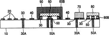
如图2A所示,按照本发明的该有源智能天线系统包括:一用于接收信号的天线100;一用于放大通过天线接收到的信号从而最小化噪声发生的低噪声放大器(LNA)200;和一用于控制由LNA200放大的信号的相位的移相器300。这里,天线100、LNA200和移相器300由各种组件构成并被形成在一块高阻基板上。
本发明的有源智能天线系统的制造方法说明如下。
首先,由导电材料诸如铜形成的导电层被形成在高阻基板10上。较佳地,高阻基板10从高阻硅基板、高阻陶瓷基板和印刷电路板(PCB)中选择。
形成在高阻基板上的导电层形成图案,从而形成天线结构材料20,并且形成构成移相器和低噪声放大器的信号电极30、接地电极50和电感40。这里,优选地,由天线结构材料20构成的天线100是平板天线(patch antenna)或槽形天线(slot antenna)。优选地,电感40是条线电感(strip 1ine inductor)或螺旋电感(spiral inductor)。
通过使用微机电系统(MEMS),电感40能够被精密地制造。基于此,电感40具有比常规电感的品质因数更高的品质因数(例如,50~60)。
在形成有信号电极30和接地电极50的高阻基板10上,形成有通孔并且该通孔被电镀,从而形成一通孔信号电极30A和通孔接地电极50A。因此,在本发明的有源智能天线系统中,形成在高阻基板的上和下表面的信号电极30可以通过通孔电极30A被彼此电连接。
为了连接电子开关60,诸如PIN型二极管、高电子迁移率晶体管(HEMT)、场效晶体管(FET)等,到形成在高阻基板10上的信号电极30,电子开关60以裸芯片的形式被安装在接地电极50上。亦即,为了应用引线接合工艺,其上具有信号电极30的裸芯片形式的电子开关60被附着在接地电极50之上(采用导电粘合剂物理接合)。接下来,由铝或金制成的接合线60A通过加热或超声波被粘合在形成在电子开关60上的信号电极30和形成在高阻基板10上的信号电极30上。这里,通过使用接合线60A,裸芯片形式的电子开关60被直接连接在高阻基板10,诸如PCB上,该方法被称为板上芯片(COB)技术,是本领域技术人员的公知常识。
一个电容70通过使用常规表面安装工艺(SMT)被连接到高阻基板10上的信号电极30。优选地,该电容70为薄膜式电容。
同时,低噪声放大器200,按照将移相器300的电子开关60连接到形成在高阻基板10上的信号电极30的方法相同的方式,将晶体管80连接到形成在高阻基板10上的信号电极30。
天线100、低噪声放大器200和移相器300被同时形成在一块高阻基板10上的按照本发明的有源智能天线系统的各种形式将参照附图进行说明。
如图2B所示,在按照本发明的有源智能天线系统中,图2A的裸芯片形式的电子开关60通过倒装接合工艺而不是引线接合工艺被连接到形成在高阻基板10上的信号电极30。
在按照本发明的有源智能天线系统中,裸芯片形式的电子开关60的尺寸稍微增大。但是,因为电子开关60通过使用比接合线物理稳定性更好的粘合剂被连接到信号电极30和接地电极50,所以形成了具有更低次品率的更稳定的结构并且降低了制造成本。
在按照本发明的该有源智能天线系统中,具有两个表面的廉价的基板被用作高阻基板。然而,为了减小移相器300的体积,多层基板可以被用来替换具有两个表面的廉价基板作为高阻基板10。下文中,将解释使用多层基板的有源智能天线系统的结构。
如图2C所示,在按照本发明的该有源智能天线系统中,图2A的电感40被叠置在高阻基板10内。这里,优选地,高阻基板10是环氧(Epoxy)PCB,聚四氟乙烯(Teflon)PCB和低温共烧陶瓷(LTCC)PCB其中之一。
按照本发明的该有源智能天线系统,电感40被叠置在高阻基板10内,使得移相器300的结构面积被减小,进而使整体结构被极大地减小。
如图2D所示,在本发明的该有源智能天线系统中,图2C的裸芯片形式的电子开关60通过倒装接合工艺而不是引线接合工艺被连接到形成在高阻基板10上的信号电极30。
按照本发明的该有源智能天线系统,电感40被叠置在高阻基板10内,并且裸芯片形式的电子开关60通过倒装接合工艺被连接到形成在高阻基板10上的信号电极30,从而减小移相器300的结构面积,形成了具有低次品率的稳定系统结构,以及降低了制造成本。
如图2E和2F所示,在本发明的该有源智能天线系统中,聚合保护材料90,诸如环氧树脂,被涂覆在裸芯片形式的电子开关60放置的部位上。因此,结构稳定的有源智能天线系统能够被实现。这里,聚合保护材料90能够被部分地涂覆从而增强物理性脆弱部分诸如裸芯片形式的电子开关60,或者能够被涂覆到高阻基板10的整个表面上。
下文中将解释为了降低制造成本将所有的信号电极30和电感40都形成在高阻基板10上的按照本发明的有源智能天线系统。
如图2G和2H所示,在本发明的该有源智能天线系统中,信号电极30和电感40被形成在高阻基板10上,不需要在高阻基板10上形成通孔并且不需要在高阻基板10内叠置电感40。因此,高阻基板10的制造成本和制造时间能够被减小。
下文中将解释能够减少可由裸芯片形式的电子开关60和晶体管80的高度造成的引线电感的本发明的一种有源智能天线系统。
如图21所示,裸芯片形式的电子开关60和晶体管80要被安装的部分的高阻基板10按照预定的高度进行蚀刻。然后,裸芯片形式的电子开关60和晶体管80被分别安装在蚀刻部分。因此,裸芯片形式的电子开关60和信号电极30之间的间隔以及晶体管80和信号电极30之间的间隔被减小,从而因引线电感的降低提高系统的性能。
如上所述,在本发明的有源智能天线系统中,移相器、天线和低噪声放大器被同时实现在一块高阻基板上,从而降低了其制造成本。
同时,在本发明的有源智能天线系统中,移相器、天线和低噪声放大器被同时实现在一块高阻基板上,从而减小了其体积。
另外,在本发明的有源智能天线系统中,移相器、天线和低噪声放大器被同时实现在一块高阻基板上,从而提高了其质量。
在不脱离本发明的精神或者实质特征的前提下,本发明可以以几种形式实现。同时应该理解,除非另外说明,上述实施例不受任何前述细节的限制,而应该在所附权利要求书中定义的它的精神和范围内进行广义地解释,因此凡是落入该权利要求的界线或者这些界线的等价物内的所有的变化和修改都被所附权利要求包含在内。
Claims (29)
1、一种有源智能天线系统,包括:
一用于接收信号的天线;
一用于放大通过天线接收到的信号从而最小化噪声发生的低噪声放大器;和
一用于控制放大信号的相位的移相器,
其中,天线、低噪声放大器和移相器被形成在一块高阻基板上。
2、如权利要求1的有源智能天线系统,其特征在于,所述高阻基板优选地从高阻硅基板、高阻陶瓷基板和印刷电路板(PCB)中选择。
3、如权利要求2的有源智能天线系统,其特征在于,所述高阻基板是两表面具有将其上下表面连接的信号电极的基板。
4、如权利要求2的有源智能天线系统,其特征在于,所述天线是平板天线或槽形天线之一。
5、如权利要求2的有源智能天线系统,其特征在于,所述移相器是由相同导电材料分别形成的信号电极、接地电极、电感,以及连接到信号电极的一电子开关和一电容构成。
6、如权利要求5的有源智能天线系统,其特征在于,所述电感通过微机电系统(MEMS)工艺被制造为条线结构或者螺旋结构。
7、如权利要求5的有源智能天线系统,其特征在于,所述电子开关被形成为裸芯片形式,通过接合线连接到信号电极。
8、如权利要求7的有源智能天线系统,其特征在于,所述电子开关进一步还包括聚合保护材料。
9、如权利要求5的有源智能天线系统,其特征在于,在部分蚀刻高阻基板之后,所述电子开关被形成在高阻基板的蚀刻部分。
10、如权利要求5的有源智能天线系统,其特征在于,所述电子开关被形成为裸芯片形式,通过倒装接合工艺连接到信号电极。
11、如权利要求10的有源智能天线系统,其特征在于,所述电子开关还包括聚合保护材料。
12、如权利要求2的有源智能天线系统,其特征在于,所述低噪声放大器被形成为裸芯片形式,通过接合线连接到信号电极。
13、如权利要求2的有源智能天线系统,其特征在于,所述低噪声放大器被形成为裸芯片形式,通过倒装接合工艺连接到信号电极。
14、如权利要求1的有源智能天线系统,其特征在于,所述高阻基板从环氧(Epoxy)PCB,聚四氟乙烯(Teflon)PCB和低温共烧陶瓷(LTCC)PCB之中选择。
15、如权利要求11的有源智能天线系统,其特征在于,所述移相器是由相同导电材料分别形成的信号电极、接地电极、电感,以及连接到信号电极的一电子开关和一电容构成。
16、如权利要求15的有源智能天线系统,其特征在于,所述电感被叠置在高阻基板内。
17、一种用于制造有源智能天线系统的方法,其中,一用于接收信号的天线,一用于放大通过天线接收到的信号从而最小化噪声发生的低噪声放大器,和一用于控制放大信号的相位的移相器被形成在一块高阻基板上。
18、如权利要求17的方法,其特征在于,所述高阻基板为高阻硅基板、高阻陶瓷基板和印刷电路板(PCB)之一。
19、如权利要求18的方法,其特征在于,所述高阻基板是两表面具有将其上下表面连接的信号电极的基板。
20、如权利要求18的方法,包括以下步骤:
在一高阻基板表面均匀形成一导电层;
在该导电层上形成图案,从而形成信号电极,接地电极和电感;和
在接地电极和信号电极上分别形成连接到信号电极的一电子开关和一电容。
21、如权利要求20的方法,其特征在于,所述电子开关被形成为裸芯片形式,通过接合线连接到信号电极。
22、如权利要求21的方法,进一步包括用于形成保护电子开关的聚合保护材料的步骤。
23、如权利要求20的方法,其特征在于,所述电子开关被形成为裸芯片形式,通过倒装接合工艺连接到信号电极。
24、如权利要求23的方法,进一步包括用于形成保护电子开关的聚合保护材料的步骤。
25、如权利要求20的方法,其特征在于,在部分蚀刻高阻基板之后,所述电子开关被形成在高阻基板的蚀刻部分。
26、如权利要求25的方法,进一步包括用于形成保护电子开关的聚合保护材料的步骤。
27、如权利要求20的方法,进一步包括用于通过对导电层制作图案形成天线的步骤。
28、如权利要求27的方法,其特征在于,所述天线是平板天线或槽形天线之一。
29、如权利要求20的方法,进一步包括用于形成连接到信号电极的低噪声放大器的步骤。
Applications Claiming Priority (2)
| Application Number | Priority Date | Filing Date | Title |
|---|---|---|---|
| KR1020030016185A KR100548244B1 (ko) | 2003-03-14 | 2003-03-14 | 저가형 능동 스마트 안테나 시스템 및 그 제조 방법 |
| KR10-2003-0016185 | 2003-03-14 |
Publications (1)
| Publication Number | Publication Date |
|---|---|
| CN1531139A true CN1531139A (zh) | 2004-09-22 |
Family
ID=32768652
Family Applications (1)
| Application Number | Title | Priority Date | Filing Date |
|---|---|---|---|
| CNA2004100089280A Pending CN1531139A (zh) | 2003-03-14 | 2004-03-15 | 有源智能天线系统及其制造方法 |
Country Status (7)
| Country | Link |
|---|---|
| US (1) | US7365683B2 (zh) |
| EP (1) | EP1458053B1 (zh) |
| JP (1) | JP2004282752A (zh) |
| KR (1) | KR100548244B1 (zh) |
| CN (1) | CN1531139A (zh) |
| AT (1) | ATE337629T1 (zh) |
| DE (1) | DE602004002007T2 (zh) |
Cited By (6)
| Publication number | Priority date | Publication date | Assignee | Title |
|---|---|---|---|---|
| WO2009052683A1 (en) * | 2007-10-25 | 2009-04-30 | Hong Kong Applied Science And Technology Research Institute Co., Ltd. | Electronic circuit package |
| CN105186125A (zh) * | 2015-08-28 | 2015-12-23 | 上海无线电设备研究所 | 一种星载裸芯片微带天线及其制造方法 |
| CN105321937A (zh) * | 2014-06-25 | 2016-02-10 | 常州欧密格光电科技有限公司 | 超小超薄高光效侧射型高亮白光多晶led元件 |
| CN107958897A (zh) * | 2017-11-28 | 2018-04-24 | 上海旦迪通信技术有限公司 | 一种北斗lna集成模块及其制备方法 |
| CN110943299A (zh) * | 2019-11-29 | 2020-03-31 | 北京京东方传感技术有限公司 | 移相器和相控阵天线 |
| WO2021056171A1 (zh) * | 2019-09-24 | 2021-04-01 | 上海旦迪通信技术有限公司 | 基于ltcc技术的gnss射频前端模块及其制备方法 |
Families Citing this family (16)
| Publication number | Priority date | Publication date | Assignee | Title |
|---|---|---|---|---|
| WO2005074029A1 (ja) * | 2004-01-28 | 2005-08-11 | Matsushita Electric Industrial Co., Ltd. | モジュール及びこれを用いた実装構造体 |
| KR100747978B1 (ko) * | 2005-06-17 | 2007-08-08 | 엘지이노텍 주식회사 | 프론트 앤드 모듈 및 그 제조방법 |
| CN101361411A (zh) * | 2006-01-20 | 2009-02-04 | 富士通株式会社 | 芯片部件的安装构造、安装方法以及电子装置 |
| WO2008013021A1 (fr) * | 2006-07-28 | 2008-01-31 | Murata Manufacturing Co., Ltd. | Dispositif d'antenne et dispositif de communication radio |
| US8138588B2 (en) * | 2006-12-21 | 2012-03-20 | Texas Instruments Incorporated | Package stiffener and a packaged device using the same |
| US7728771B2 (en) * | 2007-07-03 | 2010-06-01 | Northrop Grumman Systems Corporation | Dual band quadpack transmit/receive module |
| US20090115051A1 (en) * | 2007-11-01 | 2009-05-07 | Lap-Wai Lydia Leung | Electronic Circuit Package |
| US20090189269A1 (en) * | 2008-01-24 | 2009-07-30 | Lap-Wai Lydia Leung | Electronic Circuit Package |
| JP5417622B2 (ja) * | 2009-08-19 | 2014-02-19 | 独立行政法人 宇宙航空研究開発機構 | アナログ・デジタル積層型可変移相器 |
| JP2012009828A (ja) * | 2010-05-26 | 2012-01-12 | Jtekt Corp | 多層回路基板 |
| WO2012013998A1 (en) * | 2010-07-28 | 2012-02-02 | Nokia Corporation . | Telecommunication apparatus and associated methods |
| JP5647023B2 (ja) * | 2011-01-31 | 2014-12-24 | 株式会社ヨコオ | 地上放送波受信用アンテナ装置及びその構成部品 |
| US9667467B2 (en) | 2015-08-25 | 2017-05-30 | The Boeing Company | Gain distribution in compact high gain phased array antenna systems and methods |
| US10256538B2 (en) | 2015-08-25 | 2019-04-09 | The Boeing Company | Integrated true time delay for broad bandwidth time control systems and methods |
| CN110741509A (zh) * | 2017-02-24 | 2020-01-31 | Ami 研发有限责任公司 | 槽线体积天线 |
| CN112103637B (zh) * | 2020-08-30 | 2022-09-02 | 西南电子技术研究所(中国电子科技集团公司第十研究所) | 模块化星载Ka频段有源相控阵天线系统 |
Family Cites Families (33)
| Publication number | Priority date | Publication date | Assignee | Title |
|---|---|---|---|---|
| JPH01233902A (ja) * | 1988-03-15 | 1989-09-19 | Matsushita Electric Works Ltd | 平面アンテナ |
| JPH03196705A (ja) * | 1989-12-26 | 1991-08-28 | Hitachi Ltd | マイクロ波集積回路とそれを用いたアクティブアンテナ及びコンバータ |
| FR2659501B1 (fr) * | 1990-03-09 | 1992-07-31 | Alcatel Espace | Systeme d'antenne imprimee active a haut rendement pour radar spatial agile. |
| JP2962771B2 (ja) * | 1990-05-29 | 1999-10-12 | 三菱電機株式会社 | 移相器 |
| JPH04352506A (ja) * | 1991-05-30 | 1992-12-07 | Mitsubishi Electric Corp | アンテナ一体化マイクロ波回路 |
| JP3130575B2 (ja) * | 1991-07-25 | 2001-01-31 | 日本電気株式会社 | マイクロ波ミリ波送受信モジュール |
| JP3288736B2 (ja) * | 1991-12-03 | 2002-06-04 | 独立行政法人通信総合研究所 | アクティブフェイズドアレイアンテナ |
| JP2840493B2 (ja) * | 1991-12-27 | 1998-12-24 | 株式会社日立製作所 | 一体型マイクロ波回路 |
| JP3141692B2 (ja) * | 1994-08-11 | 2001-03-05 | 松下電器産業株式会社 | ミリ波用検波器 |
| JPH0870216A (ja) | 1994-08-26 | 1996-03-12 | Aisin Seiki Co Ltd | 平面アンテナ |
| US5554865A (en) * | 1995-06-07 | 1996-09-10 | Hughes Aircraft Company | Integrated transmit/receive switch/low noise amplifier with dissimilar semiconductor devices |
| US6130602A (en) * | 1996-05-13 | 2000-10-10 | Micron Technology, Inc. | Radio frequency data communications device |
| US6082610A (en) | 1997-06-23 | 2000-07-04 | Ford Motor Company | Method of forming interconnections on electronic modules |
| JPH1174416A (ja) * | 1997-08-29 | 1999-03-16 | Mitsubishi Electric Corp | 半導体チップ用キャリア,半導体モジュール,半導体チップ用キャリアの製造方法,および半導体モジュールの製造方法 |
| JPH11168354A (ja) * | 1997-12-04 | 1999-06-22 | Mitsubishi Electric Corp | 可変移相器 |
| US6104343A (en) * | 1998-01-14 | 2000-08-15 | Raytheon Company | Array antenna having multiple independently steered beams |
| JP2000223906A (ja) * | 1999-01-28 | 2000-08-11 | Kyocera Corp | ハイパスフィルタおよびそれを具備する回路基板 |
| EP1152485B1 (en) * | 1999-02-15 | 2014-06-18 | National Institute of Information and Communications Technology | Radio communication device |
| JP2000278009A (ja) * | 1999-03-24 | 2000-10-06 | Nec Corp | マイクロ波・ミリ波回路装置 |
| JP2001102739A (ja) * | 1999-09-27 | 2001-04-13 | Matsushita Electric Works Ltd | チップ部品の実装方法 |
| US6249439B1 (en) * | 1999-10-21 | 2001-06-19 | Hughes Electronics Corporation | Millimeter wave multilayer assembly |
| JP2001168602A (ja) * | 1999-12-14 | 2001-06-22 | Mitsubishi Electric Corp | 反射形移相器 |
| JP2001230606A (ja) * | 2000-02-15 | 2001-08-24 | Matsushita Electric Ind Co Ltd | マイクロストリップ線路と、これを用いたマイクロ波装置 |
| JP2001230506A (ja) | 2000-02-15 | 2001-08-24 | Canon Inc | 電子機器 |
| KR100404187B1 (ko) * | 2000-07-08 | 2003-11-01 | 엘지전자 주식회사 | 카본 나노 튜브 또는 카본 나노 화이바를 이용한 인덕터 |
| WO2002023672A2 (en) * | 2000-09-15 | 2002-03-21 | Raytheon Company | Microelectromechanical phased array antenna |
| JP2002118487A (ja) * | 2000-10-06 | 2002-04-19 | Matsushita Electric Ind Co Ltd | 高周波複合スイッチモジュール |
| TW523920B (en) * | 2000-11-18 | 2003-03-11 | Lenghways Technology Co Ltd | Integrated multi-channel communication passive device manufactured by using micro-electromechanical technique |
| US6532093B2 (en) * | 2000-12-06 | 2003-03-11 | Xerox Corporation | Integrated micro-opto-electro-mechanical laser scanner |
| JP2002290143A (ja) * | 2001-03-26 | 2002-10-04 | Tdk Corp | 表面実装型アンテナ及びこれが実装された基板、並びに、表面実装型アンテナの実装方法 |
| US20030011515A1 (en) * | 2001-07-16 | 2003-01-16 | Motorola, Inc. | Apparatus for effecting transfer of electromagnetic energy |
| JP2003248054A (ja) * | 2002-02-27 | 2003-09-05 | Hitachi Ltd | モノパルスレーダ装置 |
| JP4233280B2 (ja) * | 2002-08-02 | 2009-03-04 | 株式会社沖デジタルイメージング | Ledアレイ |
-
2003
- 2003-03-14 KR KR1020030016185A patent/KR100548244B1/ko not_active IP Right Cessation
-
2004
- 2004-03-10 EP EP04005722A patent/EP1458053B1/en not_active Expired - Lifetime
- 2004-03-10 DE DE602004002007T patent/DE602004002007T2/de not_active Expired - Fee Related
- 2004-03-10 AT AT04005722T patent/ATE337629T1/de not_active IP Right Cessation
- 2004-03-12 US US10/799,902 patent/US7365683B2/en not_active Expired - Fee Related
- 2004-03-12 JP JP2004070759A patent/JP2004282752A/ja active Pending
- 2004-03-15 CN CNA2004100089280A patent/CN1531139A/zh active Pending
Cited By (7)
| Publication number | Priority date | Publication date | Assignee | Title |
|---|---|---|---|---|
| WO2009052683A1 (en) * | 2007-10-25 | 2009-04-30 | Hong Kong Applied Science And Technology Research Institute Co., Ltd. | Electronic circuit package |
| CN105321937A (zh) * | 2014-06-25 | 2016-02-10 | 常州欧密格光电科技有限公司 | 超小超薄高光效侧射型高亮白光多晶led元件 |
| CN105186125A (zh) * | 2015-08-28 | 2015-12-23 | 上海无线电设备研究所 | 一种星载裸芯片微带天线及其制造方法 |
| CN107958897A (zh) * | 2017-11-28 | 2018-04-24 | 上海旦迪通信技术有限公司 | 一种北斗lna集成模块及其制备方法 |
| WO2021056171A1 (zh) * | 2019-09-24 | 2021-04-01 | 上海旦迪通信技术有限公司 | 基于ltcc技术的gnss射频前端模块及其制备方法 |
| CN110943299A (zh) * | 2019-11-29 | 2020-03-31 | 北京京东方传感技术有限公司 | 移相器和相控阵天线 |
| US11929535B2 (en) | 2019-11-29 | 2024-03-12 | Beijing Boe Sensor Technology Co., Ltd. | Phase shifter and phased array antenna |
Also Published As
| Publication number | Publication date |
|---|---|
| DE602004002007T2 (de) | 2006-12-07 |
| KR100548244B1 (ko) | 2006-02-02 |
| EP1458053A1 (en) | 2004-09-15 |
| US20040178959A1 (en) | 2004-09-16 |
| US7365683B2 (en) | 2008-04-29 |
| EP1458053B1 (en) | 2006-08-23 |
| KR20040081638A (ko) | 2004-09-22 |
| ATE337629T1 (de) | 2006-09-15 |
| JP2004282752A (ja) | 2004-10-07 |
| DE602004002007D1 (de) | 2006-10-05 |
Similar Documents
| Publication | Publication Date | Title |
|---|---|---|
| CN1531139A (zh) | 有源智能天线系统及其制造方法 | |
| CN1296642A (zh) | 射频电路模块 | |
| CN1825697A (zh) | 天线模块及使用该天线模块的电子装置 | |
| US20120235880A1 (en) | Ultrahigh-frequency package module | |
| CN1747229A (zh) | 天线模块和具有该天线模块的电子设备 | |
| CN1694250A (zh) | 高频电路模块和无线通信设备 | |
| KR101215303B1 (ko) | 엘티씨씨 인덕터를 포함하는 전자 장치 | |
| CN1595649A (zh) | 电子元件模件及其制造方法 | |
| CN1507671A (zh) | 高频模块 | |
| CN1470070A (zh) | 包括具有嵌入式电容器的内插器的电子装置及其制作方法 | |
| CN1885851A (zh) | 无线局域网通信模块和集成芯片封装 | |
| CN1684575A (zh) | 电容器内置基板 | |
| CN1914765A (zh) | 天线装置和包括这种天线装置的便携式无线电通信设备 | |
| CN1601897A (zh) | 多路分解器和通信设备 | |
| US11575194B2 (en) | Antenna structure and antenna array | |
| CN1765162A (zh) | 多层陶瓷基板 | |
| CN1481563A (zh) | 具有扩展的表面焊接区的电容器及其制造方法 | |
| CN1577839A (zh) | 混合集成电路 | |
| CN1499714A (zh) | 双工器和组合模块 | |
| CN110165374B (zh) | 一种用于5g天线的辐射单元 | |
| CN1322390A (zh) | 贴片天线设备 | |
| CN101080851A (zh) | 双模块集成天线和无线电装置 | |
| US7216406B2 (en) | Method forming split thin film capacitors with multiple voltages | |
| CN102341895B (zh) | 半导体芯片及半导体装置 | |
| CN101064271A (zh) | 具有多重导线结构的螺旋电感元件 |
Legal Events
| Date | Code | Title | Description |
|---|---|---|---|
| C06 | Publication | ||
| PB01 | Publication | ||
| C10 | Entry into substantive examination | ||
| SE01 | Entry into force of request for substantive examination | ||
| AD01 | Patent right deemed abandoned | ||
| C20 | Patent right or utility model deemed to be abandoned or is abandoned |