CN1531139A - Active intelligent antenna system and producing method thereof - Google Patents
Active intelligent antenna system and producing method thereof Download PDFInfo
- Publication number
- CN1531139A CN1531139A CNA2004100089280A CN200410008928A CN1531139A CN 1531139 A CN1531139 A CN 1531139A CN A2004100089280 A CNA2004100089280 A CN A2004100089280A CN 200410008928 A CN200410008928 A CN 200410008928A CN 1531139 A CN1531139 A CN 1531139A
- Authority
- CN
- China
- Prior art keywords
- antenna system
- active antenna
- high resistant
- electronic switch
- signal electrode
- Prior art date
- Legal status (The legal status is an assumption and is not a legal conclusion. Google has not performed a legal analysis and makes no representation as to the accuracy of the status listed.)
- Pending
Links
Images


Classifications
-
- H—ELECTRICITY
- H01—ELECTRIC ELEMENTS
- H01Q—ANTENNAS, i.e. RADIO AERIALS
- H01Q1/00—Details of, or arrangements associated with, antennas
- H01Q1/36—Structural form of radiating elements, e.g. cone, spiral, umbrella; Particular materials used therewith
- H01Q1/38—Structural form of radiating elements, e.g. cone, spiral, umbrella; Particular materials used therewith formed by a conductive layer on an insulating support
-
- H—ELECTRICITY
- H01—ELECTRIC ELEMENTS
- H01Q—ANTENNAS, i.e. RADIO AERIALS
- H01Q21/00—Antenna arrays or systems
-
- H—ELECTRICITY
- H01—ELECTRIC ELEMENTS
- H01Q—ANTENNAS, i.e. RADIO AERIALS
- H01Q23/00—Antennas with active circuits or circuit elements integrated within them or attached to them
-
- H—ELECTRICITY
- H01—ELECTRIC ELEMENTS
- H01L—SEMICONDUCTOR DEVICES NOT COVERED BY CLASS H10
- H01L2224/00—Indexing scheme for arrangements for connecting or disconnecting semiconductor or solid-state bodies and methods related thereto as covered by H01L24/00
- H01L2224/01—Means for bonding being attached to, or being formed on, the surface to be connected, e.g. chip-to-package, die-attach, "first-level" interconnects; Manufacturing methods related thereto
- H01L2224/02—Bonding areas; Manufacturing methods related thereto
- H01L2224/04—Structure, shape, material or disposition of the bonding areas prior to the connecting process
- H01L2224/05—Structure, shape, material or disposition of the bonding areas prior to the connecting process of an individual bonding area
- H01L2224/0554—External layer
- H01L2224/0556—Disposition
- H01L2224/05568—Disposition the whole external layer protruding from the surface
-
- H—ELECTRICITY
- H01—ELECTRIC ELEMENTS
- H01L—SEMICONDUCTOR DEVICES NOT COVERED BY CLASS H10
- H01L2224/00—Indexing scheme for arrangements for connecting or disconnecting semiconductor or solid-state bodies and methods related thereto as covered by H01L24/00
- H01L2224/01—Means for bonding being attached to, or being formed on, the surface to be connected, e.g. chip-to-package, die-attach, "first-level" interconnects; Manufacturing methods related thereto
- H01L2224/02—Bonding areas; Manufacturing methods related thereto
- H01L2224/04—Structure, shape, material or disposition of the bonding areas prior to the connecting process
- H01L2224/05—Structure, shape, material or disposition of the bonding areas prior to the connecting process of an individual bonding area
- H01L2224/0554—External layer
- H01L2224/05573—Single external layer
-
- H—ELECTRICITY
- H01—ELECTRIC ELEMENTS
- H01L—SEMICONDUCTOR DEVICES NOT COVERED BY CLASS H10
- H01L2224/00—Indexing scheme for arrangements for connecting or disconnecting semiconductor or solid-state bodies and methods related thereto as covered by H01L24/00
- H01L2224/01—Means for bonding being attached to, or being formed on, the surface to be connected, e.g. chip-to-package, die-attach, "first-level" interconnects; Manufacturing methods related thereto
- H01L2224/10—Bump connectors; Manufacturing methods related thereto
- H01L2224/15—Structure, shape, material or disposition of the bump connectors after the connecting process
- H01L2224/16—Structure, shape, material or disposition of the bump connectors after the connecting process of an individual bump connector
- H01L2224/161—Disposition
- H01L2224/16151—Disposition the bump connector connecting between a semiconductor or solid-state body and an item not being a semiconductor or solid-state body, e.g. chip-to-substrate, chip-to-passive
- H01L2224/16221—Disposition the bump connector connecting between a semiconductor or solid-state body and an item not being a semiconductor or solid-state body, e.g. chip-to-substrate, chip-to-passive the body and the item being stacked
- H01L2224/16225—Disposition the bump connector connecting between a semiconductor or solid-state body and an item not being a semiconductor or solid-state body, e.g. chip-to-substrate, chip-to-passive the body and the item being stacked the item being non-metallic, e.g. insulating substrate with or without metallisation
-
- H—ELECTRICITY
- H01—ELECTRIC ELEMENTS
- H01L—SEMICONDUCTOR DEVICES NOT COVERED BY CLASS H10
- H01L2224/00—Indexing scheme for arrangements for connecting or disconnecting semiconductor or solid-state bodies and methods related thereto as covered by H01L24/00
- H01L2224/01—Means for bonding being attached to, or being formed on, the surface to be connected, e.g. chip-to-package, die-attach, "first-level" interconnects; Manufacturing methods related thereto
- H01L2224/26—Layer connectors, e.g. plate connectors, solder or adhesive layers; Manufacturing methods related thereto
- H01L2224/31—Structure, shape, material or disposition of the layer connectors after the connecting process
- H01L2224/32—Structure, shape, material or disposition of the layer connectors after the connecting process of an individual layer connector
- H01L2224/321—Disposition
- H01L2224/32151—Disposition the layer connector connecting between a semiconductor or solid-state body and an item not being a semiconductor or solid-state body, e.g. chip-to-substrate, chip-to-passive
- H01L2224/32221—Disposition the layer connector connecting between a semiconductor or solid-state body and an item not being a semiconductor or solid-state body, e.g. chip-to-substrate, chip-to-passive the body and the item being stacked
- H01L2224/32225—Disposition the layer connector connecting between a semiconductor or solid-state body and an item not being a semiconductor or solid-state body, e.g. chip-to-substrate, chip-to-passive the body and the item being stacked the item being non-metallic, e.g. insulating substrate with or without metallisation
-
- H—ELECTRICITY
- H01—ELECTRIC ELEMENTS
- H01L—SEMICONDUCTOR DEVICES NOT COVERED BY CLASS H10
- H01L2224/00—Indexing scheme for arrangements for connecting or disconnecting semiconductor or solid-state bodies and methods related thereto as covered by H01L24/00
- H01L2224/01—Means for bonding being attached to, or being formed on, the surface to be connected, e.g. chip-to-package, die-attach, "first-level" interconnects; Manufacturing methods related thereto
- H01L2224/42—Wire connectors; Manufacturing methods related thereto
- H01L2224/47—Structure, shape, material or disposition of the wire connectors after the connecting process
- H01L2224/48—Structure, shape, material or disposition of the wire connectors after the connecting process of an individual wire connector
- H01L2224/4805—Shape
- H01L2224/4809—Loop shape
- H01L2224/48091—Arched
-
- H—ELECTRICITY
- H01—ELECTRIC ELEMENTS
- H01L—SEMICONDUCTOR DEVICES NOT COVERED BY CLASS H10
- H01L2224/00—Indexing scheme for arrangements for connecting or disconnecting semiconductor or solid-state bodies and methods related thereto as covered by H01L24/00
- H01L2224/01—Means for bonding being attached to, or being formed on, the surface to be connected, e.g. chip-to-package, die-attach, "first-level" interconnects; Manufacturing methods related thereto
- H01L2224/42—Wire connectors; Manufacturing methods related thereto
- H01L2224/47—Structure, shape, material or disposition of the wire connectors after the connecting process
- H01L2224/48—Structure, shape, material or disposition of the wire connectors after the connecting process of an individual wire connector
- H01L2224/481—Disposition
- H01L2224/48151—Connecting between a semiconductor or solid-state body and an item not being a semiconductor or solid-state body, e.g. chip-to-substrate, chip-to-passive
- H01L2224/48221—Connecting between a semiconductor or solid-state body and an item not being a semiconductor or solid-state body, e.g. chip-to-substrate, chip-to-passive the body and the item being stacked
- H01L2224/48225—Connecting between a semiconductor or solid-state body and an item not being a semiconductor or solid-state body, e.g. chip-to-substrate, chip-to-passive the body and the item being stacked the item being non-metallic, e.g. insulating substrate with or without metallisation
- H01L2224/48227—Connecting between a semiconductor or solid-state body and an item not being a semiconductor or solid-state body, e.g. chip-to-substrate, chip-to-passive the body and the item being stacked the item being non-metallic, e.g. insulating substrate with or without metallisation connecting the wire to a bond pad of the item
-
- H—ELECTRICITY
- H01—ELECTRIC ELEMENTS
- H01L—SEMICONDUCTOR DEVICES NOT COVERED BY CLASS H10
- H01L2224/00—Indexing scheme for arrangements for connecting or disconnecting semiconductor or solid-state bodies and methods related thereto as covered by H01L24/00
- H01L2224/73—Means for bonding being of different types provided for in two or more of groups H01L2224/10, H01L2224/18, H01L2224/26, H01L2224/34, H01L2224/42, H01L2224/50, H01L2224/63, H01L2224/71
- H01L2224/732—Location after the connecting process
- H01L2224/73251—Location after the connecting process on different surfaces
- H01L2224/73265—Layer and wire connectors
-
- H—ELECTRICITY
- H01—ELECTRIC ELEMENTS
- H01L—SEMICONDUCTOR DEVICES NOT COVERED BY CLASS H10
- H01L2924/00—Indexing scheme for arrangements or methods for connecting or disconnecting semiconductor or solid-state bodies as covered by H01L24/00
- H01L2924/0001—Technical content checked by a classifier
- H01L2924/00014—Technical content checked by a classifier the subject-matter covered by the group, the symbol of which is combined with the symbol of this group, being disclosed without further technical details
Landscapes
- Variable-Direction Aerials And Aerial Arrays (AREA)
- Details Of Aerials (AREA)
- Input Circuits Of Receivers And Coupling Of Receivers And Audio Equipment (AREA)
Abstract
Method for controlling a diesel engine, whereby based on operating parameters an operating limit is preset. The fuel amount to be injected is limited so that the preset operating limit is maintained. A correction to the operating limit is made based on a comparison of the amount of oxygen in the exhaust gas measured with a lambda probe and the theoretical oxygen amount. As an alternative to fuel injection regulation the engine torque can be limited to a maximum value. An Independent claim is made for a device for setting a correction value for an operating limit based on measured oxygen in the exhaust compared to the set value. The invention also relates to a corresponding computer program, computer program product and digital storage medium for method implementation.
Description
Technical field
The present invention relates to antenna system, relate more specifically to a kind of active antenna system and manufacture method thereof.
Background technology
Generally speaking, in next generation communication system, antenna system is necessary core component, and is applied to high frequency band, such as mobile mother space vehicle broadcast/communication, military communication etc.Antenna system can be placed on base station or portable terminal place according to the device size of antenna.Antenna system can hold a large amount of users, thereby can increase the capacity of system.
The most crucial part of antenna system is a phase shifter.Phase shifter can accurately be followed the trail of frequency of utilization by control signal.Simultaneously, phase shifter is by being operatively connected to the switching delay phase of input signals of the inductance that constitutes phase shifter, electric capacity etc., thus the signal that can in outlet terminal, this conversion of signals be become have required phase place.The current phase shifting equipment of the most normal use on the mother space vehicle receiver is to use the passive intelligent antenna system of mechanical motor phase retardation.
But, because the passive intelligent antenna system has huge volume and expensive manufacturing cost, so its popularity rate is not high.Therefore, the exploitation with active antenna system of smaller size smaller and cheap manufacturing cost is necessary fully.The structure of active antenna system describes with reference to Fig. 1.
Figure 1 shows that the calcspar of the structure of conventional active antenna system.
As shown in the figure, this active antenna system comprises: one is used to send the antenna 100 with received signal; Thereby one is used to amplify the low noise amplifier (LNA) 200 of the signal minimum noise generation that receives by antenna; With a phase shifter 300 that is used to control the phase place of amplifying signal.
Constitute in each assembly of this active antenna system phase shifter 300 maximum that takes up space and cost that need be the highest.Phase shifter 300 mainly is divided into a bit (constituting 11.25 ° of phase transformation devices), two bits (constituting 11.25 ° and 22.5 ° of phase transformation devices), three bits (constituting 11.25 °, 22.5 ° and 45 ° of phase transformation devices), four bits (constituting 11.25 °, 22.5 °, 45 ° and 90 ° of phase transformation devices) and five bits (constituting 11.25 °, 22.5 °, 45 °, 90 ° and 180 ° of phase transformation devices).In order to realize to be used in the active antenna system on the satellite broadcast reception converter, approximately need 100 above-mentioned five bit phase shifter.
Recently, along with the development of microwave monolithic formula integrated circuit (MMIC) technology, use the phase shifter of electronic switching device such as High Electron Mobility Transistor (HEMT) and field-effect transistor (FET) to be developed and to have used the active antenna system of this phase shifter just being developed energetically.Just, an electronic switch, an inductance, an electric capacity etc. are formed on the silicon substrate (for example, the GaAs substrate), and is then packed, thereby make this phase shifter 300.The technology that is used to design the active antenna system that uses this phase shifter of making 300 in the works.
But in this active antenna system, this phase shifter 300 is by using MMIC technology, and a kind of semiconductor processes is combined in multiple arrangement on the described silicon substrate and constitutes.Therefore, manufacturing cost increases, and the quality factor of inductance (for example 8~13) reduce, thereby can not expect high-quality.
Simultaneously, in this active antenna system, not only phase shifter 300, also have antenna 100, LNA200, or transmission/receiver module all must be provided at together.Each assembly is installed on the printed circuit board (PCB) (PCB) again in addition, so is assembled.Therefore, in this active antenna system, the lead-in wire that the phase shifter 300 that is used for making is bonded on the PCB is needs, thereby the quality factor of overall volume increase and inductance are worsened.
Based on this, need a kind of active antenna system and manufacture method thereof, this system can reduce manufacturing cost, has the inductance of the high quality factor that offers this system, and is easy to encapsulate phase shifter 300, antenna 100 and LNA200.
As mentioned above, according to this active antenna system of correlation technique, phase shifter is by MMIC technology, and a kind of semiconductor processes is made, so increased manufacturing cost.
Simultaneously, according to this active antenna system of correlation technique, phase shifter is by MMIC technology, and a kind of semiconductor processes manufacturing is so reduced its quality.
And according to this active antenna system of correlation technique, phase shifter is by MMIC technology, and a kind of semiconductor processes is made, so because of being used for having increased its volume in conjunction with the individual packages of antenna, LNA or transmission/receiver module.
Summary of the invention
Therefore, an object of the present invention is to provide a kind of active antenna system and manufacture method thereof, this system can reduce manufacturing cost by realize a phase shifter, an antenna and a low noise amplifier simultaneously on a high resistant substrate.
Another object of the present invention provides a kind of active antenna system and manufacture method thereof, and this system can improve its quality by realize a phase shifter, an antenna and a low noise amplifier simultaneously on a high resistant substrate.
Another purpose of the present invention provides a kind of active antenna system and manufacture method thereof, and this system can reduce its volume by realize a phase shifter, an antenna and a low noise amplifier simultaneously on a high resistant substrate.
In order to obtain these and other advantage and according to purpose of the present invention, as being specialized here and by broad description, providing a kind of active antenna system, this system comprises: one is used for the antenna of received signal; Thereby one is used to amplify the low noise amplifier of the signal minimum noise generation that receives by antenna; With a phase shifter that is used to control the phase place of amplifying signal, wherein, antenna, low noise amplifier and phase shifter are formed on the high resistant substrate.
In order to obtain these and other advantage and according to purpose of the present invention, as being specialized here and by broad description, also provide a kind of method of making active antenna system, this method comprises, wherein, one is used for the antenna of received signal, thereby one is used to amplify the phase shifter that low noise amplifier and that the signal minimum noise that receives by antenna takes place is used to control the phase place of amplifying signal and is formed on a high resistant substrate.
Above and other objects of the present invention, feature, aspect and advantage, by the detailed description of the invention of reference below in conjunction with accompanying drawing, it is distincter to become.
Description of drawings
The accompanying drawing that is included in and is cited and constitutes a specification part for ease of further understanding the present invention illustrates embodiments of the invention and comes together to explain principle of the present invention with specification.
In the accompanying drawings:
Figure 1 shows that the calcspar of the structure of common active antenna system; With
Fig. 2 A is depicted as profile according to the various structures of active antenna system of the present invention to 2I.
Embodiment
Now will be to a preferred embodiment of the present invention will be described in detail, it is represented in the accompanying drawings for example.
Hereinafter, with reference to the accompanying drawings to reducing overall volume by on a high resistant substrate, realizing a phase shifter, an antenna and a low noise amplifier simultaneously, reduce manufacturing cost, and the active antenna system and the manufacture method thereof that improve the quality describe.
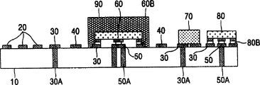
Fig. 2 A is depicted as profile according to the various structures of active antenna system of the present invention to 2I.
Shown in Fig. 2 A, comprise according to this active antenna system of the present invention: one is used for the antenna 100 of received signal; Thereby one is used to amplify the low noise amplifier (LNA) 200 of the signal minimum noise generation that receives by antenna; With a phase shifter 300 that is used to control by the phase place of LNA200 amplifying signal.Here, antenna 100, LNA200 and phase shifter 300 are made of various assemblies and are formed on the high resistant substrate.
The manufacture method of active antenna system of the present invention is described as follows.
At first, the conductive layer that is formed by electric conducting material such as copper is formed on the high resistant substrate 10.Preferably, high resistant substrate 10 is selected from High Resistivity Si substrate, high resistant ceramic substrate and printed circuit board (PCB) (PCB).
The conductive layer that is formed on the high resistant substrate forms pattern, thereby forms antenna structure material 20, and forms signal electrode 30, grounding electrode 50 and the inductance 40 that constitutes phase shifter and low noise amplifier.Here, preferably, the antenna 100 that is made of antenna structure material 20 is plate aerial (patch antenna) or slot antenna (slot antenna).Preferably, inductance 40 is bar line inductance (strip 1ine inductor) or spiral inductance (spiral inductor).
By using MEMS (micro electro mechanical system) (MEMS), inductance 40 can critically be made.Based on this, inductance 40 has the quality factor higher than the quality factor of conventional inductance (for example, 50~60).
On the high resistant substrate 10 that is formed with signal electrode 30 and grounding electrode 50, be formed with through hole and this through hole is electroplated, thereby form a through hole signal electrode 30A and through hole grounding electrode 50A.Therefore, in active antenna system of the present invention, the signal electrode 30 that is formed on the upper and lower surface of high resistant substrate can be electrically connected to each other by through hole electrode 30A.
In order to connect electronic switch 60, such as PIN type diode, High Electron Mobility Transistor (HEMT), field-effect transistor (FET) etc., to the signal electrode 30 that is formed on the high resistant substrate 10, electronic switch 60 is installed on the grounding electrode 50 with the form of bare chip.That is in order to use wire bonding technique, the electronic switch 60 that has the bare chip form of signal electrode 30 on it is attached on grounding electrode 50 and (adopts the electroconductive binder physical engagement).Next, the closing line 60A that is made by aluminium or gold is bonded to by heating or ultrasonic wave on signal electrode 30 that is formed on the electronic switch 60 and the signal electrode 30 that is formed on the high resistant substrate 10.Here, by using closing line 60A, the electronic switch 60 of bare chip form is connected directly at high resistant substrate 10, and on PCB, this method is called as chip on board (COB) technology, is those skilled in the art's common practise.
Simultaneously, low noise amplifier 200 is connected to the identical mode of method of the signal electrode 30 that is formed on the high resistant substrate 10 according to the electronic switch 60 with phase shifter 300, transistor 80 is connected to the signal electrode 30 that is formed on the high resistant substrate 10.
The various forms according to active antenna system of the present invention that antenna 100, low noise amplifier 200 and phase shifter 300 are formed on the high resistant substrate 10 simultaneously describes with reference to the accompanying drawings.
Shown in Fig. 2 B, in according to active antenna system of the present invention, the electronic switch 60 of the bare chip form of Fig. 2 A is connected to the signal electrode 30 that is formed on the high resistant substrate 10 by flip-chip bonded technology rather than wire bonding technique.
In according to active antenna system of the present invention, the size of the electronic switch 60 of bare chip form increases a little.But, because electronic switch 60 is connected to signal electrode 30 and grounding electrode 50 by using than the better adhesive of closing line physical stability, so formed more stable structure and reduced manufacturing cost with lower defect rate.
In according to this active antenna system of the present invention, the substrate with the cheapness on two surfaces is used as the high resistant substrate.Yet, in order to reduce the volume of phase shifter 300, multilager base plate can be used to replace have two surfaces cheap substrate as high resistant substrate 10.Hereinafter, the structure of the active antenna system that uses multilager base plate will be explained.
Shown in Fig. 2 C, in according to this active antenna system of the present invention, the inductance 40 of Fig. 2 A is stacked in the high resistant substrate 10.Here, preferably, high resistant substrate 10 is epoxy (Epoxy) PCB, polytetrafluoroethylene (Teflon) PCB and LTCC (LTCC) PCB one of them.
According to this active antenna system of the present invention, inductance 40 is stacked in the high resistant substrate 10, makes the structural area of phase shifter 300 be reduced, and then overall structure is greatly reduced.
Shown in Fig. 2 D, in this active antenna system of the present invention, the electronic switch 60 of the bare chip form of Fig. 2 C is connected to the signal electrode 30 that is formed on the high resistant substrate 10 by flip-chip bonded technology rather than wire bonding technique.
According to this active antenna system of the present invention, inductance 40 is stacked in the high resistant substrate 10, and the electronic switch 60 of bare chip form is connected to the signal electrode 30 that is formed on the high resistant substrate 10 by the flip-chip bonded process quilt, thereby reduce the structural area of phase shifter 300, formed systems stabilisation structure, and reduced manufacturing cost with low defect rate.
Shown in Fig. 2 E and 2F, in this active antenna system of the present invention, polymerization protective material 90 such as epoxy resin, is applied on the position that the electronic switch 60 of bare chip form places.Therefore, constitutionally stable active antenna system can be implemented.Here, thus polymerization protective material 90 can partly be applied the electronic switch 60 of the rational fragile part of reinforce such as bare chip form, perhaps can be applied on the whole surface of high resistant substrate 10.
Hereinafter will explain for reduce manufacturing cost with all signal electrodes 30 and inductance 40 all be formed on the high resistant substrate 10 according to active antenna system of the present invention.
Shown in Fig. 2 G and 2H, in this active antenna system of the present invention, signal electrode 30 and inductance 40 are formed on the high resistant substrate 10, not need form on the high resistant substrate 10 through hole and need be in high resistant substrate 10 stacked inductance 40.Therefore, the manufacturing cost of high resistant substrate 10 and manufacturing time can be reduced.
Hereinafter will explain of the present invention a kind of active antenna system that can reduce the lead-in inductance that can cause by the height of the electronic switch 60 of bare chip form and transistor 80.
As shown in figure 21, the high resistant substrate 10 of the electronic switch 60 of bare chip form and transistor 80 parts to be installed carries out etching according to predetermined height.Then, the electronic switch 60 of bare chip form and transistor 80 are mounted respectively at etching part.Therefore, the interval between the electronic switch 60 of bare chip form and the interval between the signal electrode 30 and transistor 80 and the signal electrode 30 is reduced, thereby improves the performance of system because of the reduction of lead-in inductance.
As mentioned above, in active antenna system of the present invention, phase shifter, antenna and low noise amplifier are implemented on the high resistant substrate simultaneously, thereby have reduced its manufacturing cost.
Simultaneously, in active antenna system of the present invention, phase shifter, antenna and low noise amplifier are implemented on the high resistant substrate simultaneously, thereby have reduced its volume.
In addition, in active antenna system of the present invention, phase shifter, antenna and low noise amplifier are implemented on the high resistant substrate simultaneously, thereby have improved its quality.
Under the prerequisite that does not break away from spirit of the present invention or inner characteristic, the present invention can realize with several forms.Should be appreciated that simultaneously, unless otherwise indicated, the foregoing description is not subjected to the restriction of any aforementioned details, and broadly explain in its spirit and scope that should in appended claims, define, in all variations in the equivalent in therefore every boundary line that falls into this claim or these boundary lines and revising all are included in by claims.
Claims (29)
1, a kind of active antenna system comprises:
One is used for the antenna of received signal;
Thereby one is used to amplify the low noise amplifier of the signal minimum noise generation that receives by antenna; With
One is used to control the phase shifter of the phase place of amplifying signal,
Wherein, antenna, low noise amplifier and phase shifter are formed on the high resistant substrate.
2, active antenna system as claimed in claim 1 is characterized in that, described high resistant substrate is preferably selected from High Resistivity Si substrate, high resistant ceramic substrate and printed circuit board (PCB) (PCB).
3, active antenna system as claimed in claim 2 is characterized in that, described high resistant substrate is the substrate that two surfaces have the signal electrode that its upper and lower surface is connected.
4, active antenna system as claimed in claim 2 is characterized in that, described antenna is one of plate aerial or slot antenna.
5, active antenna system as claimed in claim 2 is characterized in that, described phase shifter is signal electrode, grounding electrode, the inductance that is formed respectively by same conductive, and the electronic switch and the electric capacity formation that are connected to signal electrode.
6, active antenna system as claimed in claim 5 is characterized in that, described inductance is fabricated to bar line structure or helical structure by MEMS (micro electro mechanical system) (MEMS) process quilt.
7, active antenna system as claimed in claim 5 is characterized in that, described electronic switch is formed the bare chip form, is connected to signal electrode by closing line.
8, active antenna system as claimed in claim 7 is characterized in that, described electronic switch further comprises the polymerization protective material.
9, active antenna system as claimed in claim 5 is characterized in that, after partially-etched high resistant substrate, described electronic switch is formed on the etching part of high resistant substrate.
10, active antenna system as claimed in claim 5 is characterized in that, described electronic switch is formed the bare chip form, is connected to signal electrode by flip-chip bonded technology.
As the active antenna system of claim 10, it is characterized in that 11, described electronic switch also comprises the polymerization protective material.
12, active antenna system as claimed in claim 2 is characterized in that, described low noise amplifier is formed the bare chip form, is connected to signal electrode by closing line.
13, active antenna system as claimed in claim 2 is characterized in that, described low noise amplifier is formed the bare chip form, is connected to signal electrode by flip-chip bonded technology.
14, active antenna system as claimed in claim 1 is characterized in that, described high resistant substrate is selected among polytetrafluoroethylene (Teflon) PCB and LTCC (LTCC) PCB from epoxy (Epoxy) PCB.
As the active antenna system of claim 11, it is characterized in that 15, described phase shifter is signal electrode, grounding electrode, the inductance that is formed respectively by same conductive, and the electronic switch and the electric capacity formation that are connected to signal electrode.
As the active antenna system of claim 15, it is characterized in that 16, described inductance is stacked in the high resistant substrate.
17, a kind of method that is used to make active antenna system, wherein, one is used for the antenna of received signal, be formed on a high resistant substrate thereby one is used to amplify the phase shifter that low noise amplifier and that the signal minimum noise that receives by antenna takes place is used to control the phase place of amplifying signal.
As the method for claim 17, it is characterized in that 18, described high resistant substrate is one of High Resistivity Si substrate, high resistant ceramic substrate and printed circuit board (PCB) (PCB).
As the method for claim 18, it is characterized in that 19, described high resistant substrate is the substrate that two surfaces have the signal electrode that its upper and lower surface is connected.
20, as the method for claim 18, may further comprise the steps:
Evenly form a conductive layer at a high resistant substrate surface;
On this conductive layer, form pattern, thereby form signal electrode, grounding electrode and inductance; With
On grounding electrode and signal electrode, form an electronic switch and an electric capacity that is connected to signal electrode respectively.
As the method for claim 20, it is characterized in that 21, described electronic switch is formed the bare chip form, is connected to signal electrode by closing line.
22,, further comprise the step of the polymerization protective material that is used to form the protection electronic switch as the method for claim 21.
As the method for claim 20, it is characterized in that 23, described electronic switch is formed the bare chip form, be connected to signal electrode by flip-chip bonded technology.
24,, further comprise the step of the polymerization protective material that is used to form the protection electronic switch as the method for claim 23.
As the method for claim 20, it is characterized in that 25, after partially-etched high resistant substrate, described electronic switch is formed on the etching part of high resistant substrate.
26,, further comprise the step of the polymerization protective material that is used to form the protection electronic switch as the method for claim 25.
27,, further comprise being used for by conductive layer pattern-making being formed the step of antenna as the method for claim 20.
As the method for claim 27, it is characterized in that 28, described antenna is one of plate aerial or slot antenna.
29, as the method for claim 20, further comprise the step that is used to form the low noise amplifier that is connected to signal electrode.
Applications Claiming Priority (2)
| Application Number | Priority Date | Filing Date | Title |
|---|---|---|---|
| KR1020030016185A KR100548244B1 (en) | 2003-03-14 | 2003-03-14 | Low cost active smart antenna system amd manufacturing method thereof |
| KR10-2003-0016185 | 2003-03-14 |
Publications (1)
| Publication Number | Publication Date |
|---|---|
| CN1531139A true CN1531139A (en) | 2004-09-22 |
Family
ID=32768652
Family Applications (1)
| Application Number | Title | Priority Date | Filing Date |
|---|---|---|---|
| CNA2004100089280A Pending CN1531139A (en) | 2003-03-14 | 2004-03-15 | Active intelligent antenna system and producing method thereof |
Country Status (7)
| Country | Link |
|---|---|
| US (1) | US7365683B2 (en) |
| EP (1) | EP1458053B1 (en) |
| JP (1) | JP2004282752A (en) |
| KR (1) | KR100548244B1 (en) |
| CN (1) | CN1531139A (en) |
| AT (1) | ATE337629T1 (en) |
| DE (1) | DE602004002007T2 (en) |
Cited By (6)
| Publication number | Priority date | Publication date | Assignee | Title |
|---|---|---|---|---|
| WO2009052683A1 (en) * | 2007-10-25 | 2009-04-30 | Hong Kong Applied Science And Technology Research Institute Co., Ltd. | Electronic circuit package |
| CN105186125A (en) * | 2015-08-28 | 2015-12-23 | 上海无线电设备研究所 | Satellite-borne bare chip microstrip antenna and manufacturing method thereof |
| CN105321937A (en) * | 2014-06-25 | 2016-02-10 | 常州欧密格光电科技有限公司 | Ultra small and ultrathin high luminous efficiency lateral emission type high light white light polycrystalline LED element |
| CN107958897A (en) * | 2017-11-28 | 2018-04-24 | 上海旦迪通信技术有限公司 | A kind of Big Dipper LNA integration modules and preparation method thereof |
| CN110943299A (en) * | 2019-11-29 | 2020-03-31 | 北京京东方传感技术有限公司 | Phase shifter and phased array antenna |
| WO2021056171A1 (en) * | 2019-09-24 | 2021-04-01 | 上海旦迪通信技术有限公司 | Gnss radio frequency front-end module based on ltcc technology and preparation method therefor |
Families Citing this family (16)
| Publication number | Priority date | Publication date | Assignee | Title |
|---|---|---|---|---|
| US7667974B2 (en) * | 2004-01-28 | 2010-02-23 | Panasonic Corporation | Module and mounted structure using the same |
| KR100747978B1 (en) * | 2005-06-17 | 2007-08-08 | 엘지이노텍 주식회사 | Front end module and fabricating method thereof |
| EP1976354A4 (en) * | 2006-01-20 | 2012-08-01 | Fujitsu Ltd | Chip component mounting structure, chip component mounting method and electronic device |
| CN101496224B (en) * | 2006-07-28 | 2012-12-12 | 株式会社村田制作所 | Antenna device and radio communication device |
| US8138588B2 (en) * | 2006-12-21 | 2012-03-20 | Texas Instruments Incorporated | Package stiffener and a packaged device using the same |
| US7728771B2 (en) * | 2007-07-03 | 2010-06-01 | Northrop Grumman Systems Corporation | Dual band quadpack transmit/receive module |
| US20090115051A1 (en) * | 2007-11-01 | 2009-05-07 | Lap-Wai Lydia Leung | Electronic Circuit Package |
| US20090189269A1 (en) * | 2008-01-24 | 2009-07-30 | Lap-Wai Lydia Leung | Electronic Circuit Package |
| JP5417622B2 (en) * | 2009-08-19 | 2014-02-19 | 独立行政法人 宇宙航空研究開発機構 | Analog / digital stacked variable phase shifter |
| JP2012009828A (en) * | 2010-05-26 | 2012-01-12 | Jtekt Corp | Multilayer circuit board |
| EP2599366A4 (en) * | 2010-07-28 | 2014-12-24 | Nokia Corp | Telecommunication apparatus and associated methods |
| JP5647023B2 (en) * | 2011-01-31 | 2014-12-24 | 株式会社ヨコオ | Terrestrial broadcast wave receiving antenna device and components thereof |
| US10256538B2 (en) * | 2015-08-25 | 2019-04-09 | The Boeing Company | Integrated true time delay for broad bandwidth time control systems and methods |
| US9667467B2 (en) | 2015-08-25 | 2017-05-30 | The Boeing Company | Gain distribution in compact high gain phased array antenna systems and methods |
| CN110741509A (en) * | 2017-02-24 | 2020-01-31 | Ami 研发有限责任公司 | Slot line volume antenna |
| CN112103637B (en) * | 2020-08-30 | 2022-09-02 | 西南电子技术研究所(中国电子科技集团公司第十研究所) | Modularized satellite-borne Ka-frequency-band active phased-array antenna system |
Family Cites Families (33)
| Publication number | Priority date | Publication date | Assignee | Title |
|---|---|---|---|---|
| JPH01233902A (en) | 1988-03-15 | 1989-09-19 | Matsushita Electric Works Ltd | Planar antenna |
| JPH03196705A (en) | 1989-12-26 | 1991-08-28 | Hitachi Ltd | Microwave integrated circuit and active antenna and converter using the circuit |
| FR2659501B1 (en) * | 1990-03-09 | 1992-07-31 | Alcatel Espace | HIGH EFFICIENCY PRINTED ACTIVE ANTENNA SYSTEM FOR AGILE SPATIAL RADAR. |
| JP2962771B2 (en) | 1990-05-29 | 1999-10-12 | 三菱電機株式会社 | Phase shifter |
| JPH04352506A (en) | 1991-05-30 | 1992-12-07 | Mitsubishi Electric Corp | Microwave circuit with integrated antenna |
| JP3130575B2 (en) * | 1991-07-25 | 2001-01-31 | 日本電気株式会社 | Microwave and millimeter wave transceiver module |
| JP3288736B2 (en) | 1991-12-03 | 2002-06-04 | 独立行政法人通信総合研究所 | Active phased array antenna |
| JP2840493B2 (en) * | 1991-12-27 | 1998-12-24 | 株式会社日立製作所 | Integrated microwave circuit |
| JP3141692B2 (en) * | 1994-08-11 | 2001-03-05 | 松下電器産業株式会社 | Millimeter wave detector |
| JPH0870216A (en) | 1994-08-26 | 1996-03-12 | Aisin Seiki Co Ltd | Plane antenna |
| US5554865A (en) * | 1995-06-07 | 1996-09-10 | Hughes Aircraft Company | Integrated transmit/receive switch/low noise amplifier with dissimilar semiconductor devices |
| US6130602A (en) * | 1996-05-13 | 2000-10-10 | Micron Technology, Inc. | Radio frequency data communications device |
| US6082610A (en) | 1997-06-23 | 2000-07-04 | Ford Motor Company | Method of forming interconnections on electronic modules |
| JPH1174416A (en) * | 1997-08-29 | 1999-03-16 | Mitsubishi Electric Corp | Semiconductor chip carrier and semiconductor module, and manufacture of these two |
| JPH11168354A (en) | 1997-12-04 | 1999-06-22 | Mitsubishi Electric Corp | Variable phase shifter |
| US6104343A (en) * | 1998-01-14 | 2000-08-15 | Raytheon Company | Array antenna having multiple independently steered beams |
| JP2000223906A (en) | 1999-01-28 | 2000-08-11 | Kyocera Corp | High-pass filter and circuit board equipped with same |
| WO2000048269A1 (en) * | 1999-02-15 | 2000-08-17 | Communications Research Laboratory, Independent Administrative Institution | Radio communication device |
| JP2000278009A (en) * | 1999-03-24 | 2000-10-06 | Nec Corp | Microwave/millimeter wave circuit device |
| JP2001102739A (en) | 1999-09-27 | 2001-04-13 | Matsushita Electric Works Ltd | Method of mounting chip component |
| US6249439B1 (en) * | 1999-10-21 | 2001-06-19 | Hughes Electronics Corporation | Millimeter wave multilayer assembly |
| JP2001168602A (en) | 1999-12-14 | 2001-06-22 | Mitsubishi Electric Corp | Reflection type phase shifter |
| JP2001230506A (en) | 2000-02-15 | 2001-08-24 | Canon Inc | Electronic apparatus |
| JP2001230606A (en) * | 2000-02-15 | 2001-08-24 | Matsushita Electric Ind Co Ltd | Microstrip line and microwave device using the same |
| KR100404187B1 (en) * | 2000-07-08 | 2003-11-01 | 엘지전자 주식회사 | inductor using carbon nano tube or carbon nano fiber |
| US6653985B2 (en) * | 2000-09-15 | 2003-11-25 | Raytheon Company | Microelectromechanical phased array antenna |
| JP2002118487A (en) * | 2000-10-06 | 2002-04-19 | Matsushita Electric Ind Co Ltd | High-frequency composite switch module |
| TW523920B (en) * | 2000-11-18 | 2003-03-11 | Lenghways Technology Co Ltd | Integrated multi-channel communication passive device manufactured by using micro-electromechanical technique |
| US6532093B2 (en) | 2000-12-06 | 2003-03-11 | Xerox Corporation | Integrated micro-opto-electro-mechanical laser scanner |
| JP2002290143A (en) | 2001-03-26 | 2002-10-04 | Tdk Corp | Surface-mounted antenna, substrate on which the same is mounted and mounting method of the surface-mounted antenna |
| US20030011515A1 (en) * | 2001-07-16 | 2003-01-16 | Motorola, Inc. | Apparatus for effecting transfer of electromagnetic energy |
| JP2003248054A (en) * | 2002-02-27 | 2003-09-05 | Hitachi Ltd | Monopulse radar apparatus |
| JP4233280B2 (en) * | 2002-08-02 | 2009-03-04 | 株式会社沖デジタルイメージング | LED array |
-
2003
- 2003-03-14 KR KR1020030016185A patent/KR100548244B1/en not_active IP Right Cessation
-
2004
- 2004-03-10 AT AT04005722T patent/ATE337629T1/en not_active IP Right Cessation
- 2004-03-10 EP EP04005722A patent/EP1458053B1/en not_active Expired - Lifetime
- 2004-03-10 DE DE602004002007T patent/DE602004002007T2/en not_active Expired - Fee Related
- 2004-03-12 US US10/799,902 patent/US7365683B2/en not_active Expired - Fee Related
- 2004-03-12 JP JP2004070759A patent/JP2004282752A/en active Pending
- 2004-03-15 CN CNA2004100089280A patent/CN1531139A/en active Pending
Cited By (7)
| Publication number | Priority date | Publication date | Assignee | Title |
|---|---|---|---|---|
| WO2009052683A1 (en) * | 2007-10-25 | 2009-04-30 | Hong Kong Applied Science And Technology Research Institute Co., Ltd. | Electronic circuit package |
| CN105321937A (en) * | 2014-06-25 | 2016-02-10 | 常州欧密格光电科技有限公司 | Ultra small and ultrathin high luminous efficiency lateral emission type high light white light polycrystalline LED element |
| CN105186125A (en) * | 2015-08-28 | 2015-12-23 | 上海无线电设备研究所 | Satellite-borne bare chip microstrip antenna and manufacturing method thereof |
| CN107958897A (en) * | 2017-11-28 | 2018-04-24 | 上海旦迪通信技术有限公司 | A kind of Big Dipper LNA integration modules and preparation method thereof |
| WO2021056171A1 (en) * | 2019-09-24 | 2021-04-01 | 上海旦迪通信技术有限公司 | Gnss radio frequency front-end module based on ltcc technology and preparation method therefor |
| CN110943299A (en) * | 2019-11-29 | 2020-03-31 | 北京京东方传感技术有限公司 | Phase shifter and phased array antenna |
| US11929535B2 (en) | 2019-11-29 | 2024-03-12 | Beijing Boe Sensor Technology Co., Ltd. | Phase shifter and phased array antenna |
Also Published As
| Publication number | Publication date |
|---|---|
| DE602004002007D1 (en) | 2006-10-05 |
| EP1458053B1 (en) | 2006-08-23 |
| EP1458053A1 (en) | 2004-09-15 |
| KR20040081638A (en) | 2004-09-22 |
| KR100548244B1 (en) | 2006-02-02 |
| US20040178959A1 (en) | 2004-09-16 |
| DE602004002007T2 (en) | 2006-12-07 |
| US7365683B2 (en) | 2008-04-29 |
| JP2004282752A (en) | 2004-10-07 |
| ATE337629T1 (en) | 2006-09-15 |
Similar Documents
| Publication | Publication Date | Title |
|---|---|---|
| CN1531139A (en) | Active intelligent antenna system and producing method thereof | |
| CN1663120A (en) | Electronic component comprising a multilayer substrate and corresponding method of production | |
| CN1296642A (en) | RF circuit module | |
| CN1825697A (en) | Antenna module and electronic arrangement using same | |
| US20120235880A1 (en) | Ultrahigh-frequency package module | |
| CN1747229A (en) | Antenna module and elctronic apparatus having the same | |
| CN1694250A (en) | High-frequency circuit module and radio communication apparatus | |
| CN1507671A (en) | High frequency module | |
| US8044757B2 (en) | Electronic device including LTCC inductor | |
| CN1470070A (en) | Electronic assembly comprising interposer with embedded capacitors and methods of manufacture | |
| CN1885851A (en) | Wireless local area network communications module and integrated chip package | |
| CN1684575A (en) | Capacitor-embedded substrate | |
| CN1914765A (en) | Antenna device and portable radio communication device comprising such an antenna device | |
| CN1601897A (en) | Demultiplexer and communications device | |
| US11575194B2 (en) | Antenna structure and antenna array | |
| CN1765162A (en) | Ceramic multilayer substrate | |
| CN100341243C (en) | Duplexer and combined modular | |
| CN1481563A (en) | Capacitor with extended surface lands and method of fabrication therefor | |
| CN1577839A (en) | Hybrid integrated circuit | |
| CN110165374B (en) | Radiation unit for 5G antenna | |
| CN101080851A (en) | A two-module integrated antenna and radio | |
| US7216406B2 (en) | Method forming split thin film capacitors with multiple voltages | |
| CN102341895B (en) | Semiconductor chip and semiconductor device | |
| CN101064271A (en) | Screw inductive element having multiplex conductor structure | |
| US6933596B2 (en) | Ultra wideband BGA |
Legal Events
| Date | Code | Title | Description |
|---|---|---|---|
| C06 | Publication | ||
| PB01 | Publication | ||
| C10 | Entry into substantive examination | ||
| SE01 | Entry into force of request for substantive examination | ||
| AD01 | Patent right deemed abandoned | ||
| C20 | Patent right or utility model deemed to be abandoned or is abandoned |