CN116349006A - 半导体装置 - Google Patents
半导体装置 Download PDFInfo
- Publication number
- CN116349006A CN116349006A CN202180072875.0A CN202180072875A CN116349006A CN 116349006 A CN116349006 A CN 116349006A CN 202180072875 A CN202180072875 A CN 202180072875A CN 116349006 A CN116349006 A CN 116349006A
- Authority
- CN
- China
- Prior art keywords
- region
- trench
- semiconductor device
- semiconductor substrate
- gate
- Prior art date
- Legal status (The legal status is an assumption and is not a legal conclusion. Google has not performed a legal analysis and makes no representation as to the accuracy of the status listed.)
- Pending
Links
- 239000004065 semiconductor Substances 0.000 title claims abstract description 139
- 239000000758 substrate Substances 0.000 claims abstract description 81
- 238000009825 accumulation Methods 0.000 claims description 23
- 239000000370 acceptor Substances 0.000 description 19
- 239000011229 interlayer Substances 0.000 description 18
- 239000010410 layer Substances 0.000 description 17
- 229910052751 metal Inorganic materials 0.000 description 14
- 239000002184 metal Substances 0.000 description 14
- 238000000034 method Methods 0.000 description 12
- 239000012535 impurity Substances 0.000 description 9
- 238000010586 diagram Methods 0.000 description 8
- 230000004888 barrier function Effects 0.000 description 6
- 230000005684 electric field Effects 0.000 description 5
- 229910021420 polycrystalline silicon Inorganic materials 0.000 description 5
- 229920005591 polysilicon Polymers 0.000 description 5
- 239000000126 substance Substances 0.000 description 5
- 230000001052 transient effect Effects 0.000 description 5
- XUIMIQQOPSSXEZ-UHFFFAOYSA-N Silicon Chemical compound [Si] XUIMIQQOPSSXEZ-UHFFFAOYSA-N 0.000 description 4
- 229910052782 aluminium Inorganic materials 0.000 description 4
- XAGFODPZIPBFFR-UHFFFAOYSA-N aluminium Chemical compound [Al] XAGFODPZIPBFFR-UHFFFAOYSA-N 0.000 description 4
- 229910052710 silicon Inorganic materials 0.000 description 4
- 239000010703 silicon Substances 0.000 description 4
- WFKWXMTUELFFGS-UHFFFAOYSA-N tungsten Chemical compound [W] WFKWXMTUELFFGS-UHFFFAOYSA-N 0.000 description 4
- 229910052721 tungsten Inorganic materials 0.000 description 4
- 239000010937 tungsten Substances 0.000 description 4
- OAICVXFJPJFONN-UHFFFAOYSA-N Phosphorus Chemical compound [P] OAICVXFJPJFONN-UHFFFAOYSA-N 0.000 description 3
- 239000002019 doping agent Substances 0.000 description 3
- 230000000694 effects Effects 0.000 description 3
- 229910052739 hydrogen Inorganic materials 0.000 description 3
- 239000001257 hydrogen Substances 0.000 description 3
- 239000000463 material Substances 0.000 description 3
- 150000004767 nitrides Chemical class 0.000 description 3
- 229910052698 phosphorus Inorganic materials 0.000 description 3
- 239000011574 phosphorus Substances 0.000 description 3
- 230000008569 process Effects 0.000 description 3
- UFHFLCQGNIYNRP-UHFFFAOYSA-N Hydrogen Chemical compound [H][H] UFHFLCQGNIYNRP-UHFFFAOYSA-N 0.000 description 2
- 229910052785 arsenic Inorganic materials 0.000 description 2
- RQNWIZPPADIBDY-UHFFFAOYSA-N arsenic atom Chemical compound [As] RQNWIZPPADIBDY-UHFFFAOYSA-N 0.000 description 2
- 230000007423 decrease Effects 0.000 description 2
- 230000007547 defect Effects 0.000 description 2
- 238000009792 diffusion process Methods 0.000 description 2
- 230000001747 exhibiting effect Effects 0.000 description 2
- 150000002500 ions Chemical class 0.000 description 2
- 238000005259 measurement Methods 0.000 description 2
- 238000012986 modification Methods 0.000 description 2
- 230000004048 modification Effects 0.000 description 2
- 230000000149 penetrating effect Effects 0.000 description 2
- ZOXJGFHDIHLPTG-UHFFFAOYSA-N Boron Chemical compound [B] ZOXJGFHDIHLPTG-UHFFFAOYSA-N 0.000 description 1
- 229910002601 GaN Inorganic materials 0.000 description 1
- JMASRVWKEDWRBT-UHFFFAOYSA-N Gallium nitride Chemical compound [Ga]#N JMASRVWKEDWRBT-UHFFFAOYSA-N 0.000 description 1
- 229910000676 Si alloy Inorganic materials 0.000 description 1
- RTAQQCXQSZGOHL-UHFFFAOYSA-N Titanium Chemical compound [Ti] RTAQQCXQSZGOHL-UHFFFAOYSA-N 0.000 description 1
- KPSZQYZCNSCYGG-UHFFFAOYSA-N [B].[B] Chemical compound [B].[B] KPSZQYZCNSCYGG-UHFFFAOYSA-N 0.000 description 1
- 230000004913 activation Effects 0.000 description 1
- 229910045601 alloy Inorganic materials 0.000 description 1
- 239000000956 alloy Substances 0.000 description 1
- 230000004075 alteration Effects 0.000 description 1
- CSDREXVUYHZDNP-UHFFFAOYSA-N alumanylidynesilicon Chemical compound [Al].[Si] CSDREXVUYHZDNP-UHFFFAOYSA-N 0.000 description 1
- 229910052787 antimony Inorganic materials 0.000 description 1
- WATWJIUSRGPENY-UHFFFAOYSA-N antimony atom Chemical compound [Sb] WATWJIUSRGPENY-UHFFFAOYSA-N 0.000 description 1
- QVGXLLKOCUKJST-UHFFFAOYSA-N atomic oxygen Chemical compound [O] QVGXLLKOCUKJST-UHFFFAOYSA-N 0.000 description 1
- 230000000903 blocking effect Effects 0.000 description 1
- 229910052796 boron Inorganic materials 0.000 description 1
- 239000000969 carrier Substances 0.000 description 1
- 239000004020 conductor Substances 0.000 description 1
- 239000000470 constituent Substances 0.000 description 1
- 239000013078 crystal Substances 0.000 description 1
- 238000001514 detection method Methods 0.000 description 1
- 230000005484 gravity Effects 0.000 description 1
- 230000012447 hatching Effects 0.000 description 1
- 150000002431 hydrogen Chemical class 0.000 description 1
- 238000002347 injection Methods 0.000 description 1
- 239000007924 injection Substances 0.000 description 1
- 239000011810 insulating material Substances 0.000 description 1
- 238000004519 manufacturing process Methods 0.000 description 1
- 229910052760 oxygen Inorganic materials 0.000 description 1
- 239000001301 oxygen Substances 0.000 description 1
- 230000001737 promoting effect Effects 0.000 description 1
- 238000001004 secondary ion mass spectrometry Methods 0.000 description 1
- 239000005368 silicate glass Substances 0.000 description 1
- HBMJWWWQQXIZIP-UHFFFAOYSA-N silicon carbide Chemical compound [Si+]#[C-] HBMJWWWQQXIZIP-UHFFFAOYSA-N 0.000 description 1
- 229910010271 silicon carbide Inorganic materials 0.000 description 1
- 239000002344 surface layer Substances 0.000 description 1
- 239000010936 titanium Substances 0.000 description 1
- 229910052719 titanium Inorganic materials 0.000 description 1
- 150000003609 titanium compounds Chemical class 0.000 description 1
Images


Classifications
-
- H—ELECTRICITY
- H01—ELECTRIC ELEMENTS
- H01L—SEMICONDUCTOR DEVICES NOT COVERED BY CLASS H10
- H01L29/00—Semiconductor devices specially adapted for rectifying, amplifying, oscillating or switching and having potential barriers; Capacitors or resistors having potential barriers, e.g. a PN-junction depletion layer or carrier concentration layer; Details of semiconductor bodies or of electrodes thereof ; Multistep manufacturing processes therefor
- H01L29/66—Types of semiconductor device ; Multistep manufacturing processes therefor
- H01L29/86—Types of semiconductor device ; Multistep manufacturing processes therefor controllable only by variation of the electric current supplied, or only the electric potential applied, to one or more of the electrodes carrying the current to be rectified, amplified, oscillated or switched
- H01L29/861—Diodes
- H01L29/8613—Mesa PN junction diodes
-
- H—ELECTRICITY
- H01—ELECTRIC ELEMENTS
- H01L—SEMICONDUCTOR DEVICES NOT COVERED BY CLASS H10
- H01L29/00—Semiconductor devices specially adapted for rectifying, amplifying, oscillating or switching and having potential barriers; Capacitors or resistors having potential barriers, e.g. a PN-junction depletion layer or carrier concentration layer; Details of semiconductor bodies or of electrodes thereof ; Multistep manufacturing processes therefor
- H01L29/02—Semiconductor bodies ; Multistep manufacturing processes therefor
- H01L29/06—Semiconductor bodies ; Multistep manufacturing processes therefor characterised by their shape; characterised by the shapes, relative sizes, or dispositions of the semiconductor regions ; characterised by the concentration or distribution of impurities within semiconductor regions
- H01L29/0603—Semiconductor bodies ; Multistep manufacturing processes therefor characterised by their shape; characterised by the shapes, relative sizes, or dispositions of the semiconductor regions ; characterised by the concentration or distribution of impurities within semiconductor regions characterised by particular constructional design considerations, e.g. for preventing surface leakage, for controlling electric field concentration or for internal isolations regions
- H01L29/0607—Semiconductor bodies ; Multistep manufacturing processes therefor characterised by their shape; characterised by the shapes, relative sizes, or dispositions of the semiconductor regions ; characterised by the concentration or distribution of impurities within semiconductor regions characterised by particular constructional design considerations, e.g. for preventing surface leakage, for controlling electric field concentration or for internal isolations regions for preventing surface leakage or controlling electric field concentration
- H01L29/0611—Semiconductor bodies ; Multistep manufacturing processes therefor characterised by their shape; characterised by the shapes, relative sizes, or dispositions of the semiconductor regions ; characterised by the concentration or distribution of impurities within semiconductor regions characterised by particular constructional design considerations, e.g. for preventing surface leakage, for controlling electric field concentration or for internal isolations regions for preventing surface leakage or controlling electric field concentration for increasing or controlling the breakdown voltage of reverse biased devices
- H01L29/0615—Semiconductor bodies ; Multistep manufacturing processes therefor characterised by their shape; characterised by the shapes, relative sizes, or dispositions of the semiconductor regions ; characterised by the concentration or distribution of impurities within semiconductor regions characterised by particular constructional design considerations, e.g. for preventing surface leakage, for controlling electric field concentration or for internal isolations regions for preventing surface leakage or controlling electric field concentration for increasing or controlling the breakdown voltage of reverse biased devices by the doping profile or the shape or the arrangement of the PN junction, or with supplementary regions, e.g. junction termination extension [JTE]
- H01L29/0619—Semiconductor bodies ; Multistep manufacturing processes therefor characterised by their shape; characterised by the shapes, relative sizes, or dispositions of the semiconductor regions ; characterised by the concentration or distribution of impurities within semiconductor regions characterised by particular constructional design considerations, e.g. for preventing surface leakage, for controlling electric field concentration or for internal isolations regions for preventing surface leakage or controlling electric field concentration for increasing or controlling the breakdown voltage of reverse biased devices by the doping profile or the shape or the arrangement of the PN junction, or with supplementary regions, e.g. junction termination extension [JTE] with a supplementary region doped oppositely to or in rectifying contact with the semiconductor containing or contacting region, e.g. guard rings with PN or Schottky junction
- H01L29/0623—Buried supplementary region, e.g. buried guard ring
-
- H—ELECTRICITY
- H01—ELECTRIC ELEMENTS
- H01L—SEMICONDUCTOR DEVICES NOT COVERED BY CLASS H10
- H01L29/00—Semiconductor devices specially adapted for rectifying, amplifying, oscillating or switching and having potential barriers; Capacitors or resistors having potential barriers, e.g. a PN-junction depletion layer or carrier concentration layer; Details of semiconductor bodies or of electrodes thereof ; Multistep manufacturing processes therefor
- H01L29/02—Semiconductor bodies ; Multistep manufacturing processes therefor
- H01L29/06—Semiconductor bodies ; Multistep manufacturing processes therefor characterised by their shape; characterised by the shapes, relative sizes, or dispositions of the semiconductor regions ; characterised by the concentration or distribution of impurities within semiconductor regions
- H01L29/0684—Semiconductor bodies ; Multistep manufacturing processes therefor characterised by their shape; characterised by the shapes, relative sizes, or dispositions of the semiconductor regions ; characterised by the concentration or distribution of impurities within semiconductor regions characterised by the shape, relative sizes or dispositions of the semiconductor regions or junctions between the regions
- H01L29/0692—Surface layout
- H01L29/0696—Surface layout of cellular field-effect devices, e.g. multicellular DMOS transistors or IGBTs
-
- H—ELECTRICITY
- H01—ELECTRIC ELEMENTS
- H01L—SEMICONDUCTOR DEVICES NOT COVERED BY CLASS H10
- H01L29/00—Semiconductor devices specially adapted for rectifying, amplifying, oscillating or switching and having potential barriers; Capacitors or resistors having potential barriers, e.g. a PN-junction depletion layer or carrier concentration layer; Details of semiconductor bodies or of electrodes thereof ; Multistep manufacturing processes therefor
- H01L29/02—Semiconductor bodies ; Multistep manufacturing processes therefor
- H01L29/06—Semiconductor bodies ; Multistep manufacturing processes therefor characterised by their shape; characterised by the shapes, relative sizes, or dispositions of the semiconductor regions ; characterised by the concentration or distribution of impurities within semiconductor regions
- H01L29/10—Semiconductor bodies ; Multistep manufacturing processes therefor characterised by their shape; characterised by the shapes, relative sizes, or dispositions of the semiconductor regions ; characterised by the concentration or distribution of impurities within semiconductor regions with semiconductor regions connected to an electrode not carrying current to be rectified, amplified or switched and such electrode being part of a semiconductor device which comprises three or more electrodes
- H01L29/1095—Body region, i.e. base region, of DMOS transistors or IGBTs
-
- H—ELECTRICITY
- H01—ELECTRIC ELEMENTS
- H01L—SEMICONDUCTOR DEVICES NOT COVERED BY CLASS H10
- H01L29/00—Semiconductor devices specially adapted for rectifying, amplifying, oscillating or switching and having potential barriers; Capacitors or resistors having potential barriers, e.g. a PN-junction depletion layer or carrier concentration layer; Details of semiconductor bodies or of electrodes thereof ; Multistep manufacturing processes therefor
- H01L29/40—Electrodes ; Multistep manufacturing processes therefor
- H01L29/402—Field plates
- H01L29/407—Recessed field plates, e.g. trench field plates, buried field plates
-
- H—ELECTRICITY
- H01—ELECTRIC ELEMENTS
- H01L—SEMICONDUCTOR DEVICES NOT COVERED BY CLASS H10
- H01L29/00—Semiconductor devices specially adapted for rectifying, amplifying, oscillating or switching and having potential barriers; Capacitors or resistors having potential barriers, e.g. a PN-junction depletion layer or carrier concentration layer; Details of semiconductor bodies or of electrodes thereof ; Multistep manufacturing processes therefor
- H01L29/66—Types of semiconductor device ; Multistep manufacturing processes therefor
- H01L29/68—Types of semiconductor device ; Multistep manufacturing processes therefor controllable by only the electric current supplied, or only the electric potential applied, to an electrode which does not carry the current to be rectified, amplified or switched
- H01L29/70—Bipolar devices
- H01L29/72—Transistor-type devices, i.e. able to continuously respond to applied control signals
- H01L29/739—Transistor-type devices, i.e. able to continuously respond to applied control signals controlled by field-effect, e.g. bipolar static induction transistors [BSIT]
- H01L29/7393—Insulated gate bipolar mode transistors, i.e. IGBT; IGT; COMFET
- H01L29/7395—Vertical transistors, e.g. vertical IGBT
- H01L29/7396—Vertical transistors, e.g. vertical IGBT with a non planar surface, e.g. with a non planar gate or with a trench or recess or pillar in the surface of the emitter, base or collector region for improving current density or short circuiting the emitter and base regions
- H01L29/7397—Vertical transistors, e.g. vertical IGBT with a non planar surface, e.g. with a non planar gate or with a trench or recess or pillar in the surface of the emitter, base or collector region for improving current density or short circuiting the emitter and base regions and a gate structure lying on a slanted or vertical surface or formed in a groove, e.g. trench gate IGBT
-
- H—ELECTRICITY
- H01—ELECTRIC ELEMENTS
- H01L—SEMICONDUCTOR DEVICES NOT COVERED BY CLASS H10
- H01L27/00—Devices consisting of a plurality of semiconductor or other solid-state components formed in or on a common substrate
- H01L27/02—Devices consisting of a plurality of semiconductor or other solid-state components formed in or on a common substrate including semiconductor components specially adapted for rectifying, oscillating, amplifying or switching and having potential barriers; including integrated passive circuit elements having potential barriers
- H01L27/04—Devices consisting of a plurality of semiconductor or other solid-state components formed in or on a common substrate including semiconductor components specially adapted for rectifying, oscillating, amplifying or switching and having potential barriers; including integrated passive circuit elements having potential barriers the substrate being a semiconductor body
- H01L27/06—Devices consisting of a plurality of semiconductor or other solid-state components formed in or on a common substrate including semiconductor components specially adapted for rectifying, oscillating, amplifying or switching and having potential barriers; including integrated passive circuit elements having potential barriers the substrate being a semiconductor body including a plurality of individual components in a non-repetitive configuration
- H01L27/07—Devices consisting of a plurality of semiconductor or other solid-state components formed in or on a common substrate including semiconductor components specially adapted for rectifying, oscillating, amplifying or switching and having potential barriers; including integrated passive circuit elements having potential barriers the substrate being a semiconductor body including a plurality of individual components in a non-repetitive configuration the components having an active region in common
- H01L27/0705—Devices consisting of a plurality of semiconductor or other solid-state components formed in or on a common substrate including semiconductor components specially adapted for rectifying, oscillating, amplifying or switching and having potential barriers; including integrated passive circuit elements having potential barriers the substrate being a semiconductor body including a plurality of individual components in a non-repetitive configuration the components having an active region in common comprising components of the field effect type
- H01L27/0727—Devices consisting of a plurality of semiconductor or other solid-state components formed in or on a common substrate including semiconductor components specially adapted for rectifying, oscillating, amplifying or switching and having potential barriers; including integrated passive circuit elements having potential barriers the substrate being a semiconductor body including a plurality of individual components in a non-repetitive configuration the components having an active region in common comprising components of the field effect type in combination with diodes, or capacitors or resistors
-
- H—ELECTRICITY
- H01—ELECTRIC ELEMENTS
- H01L—SEMICONDUCTOR DEVICES NOT COVERED BY CLASS H10
- H01L29/00—Semiconductor devices specially adapted for rectifying, amplifying, oscillating or switching and having potential barriers; Capacitors or resistors having potential barriers, e.g. a PN-junction depletion layer or carrier concentration layer; Details of semiconductor bodies or of electrodes thereof ; Multistep manufacturing processes therefor
- H01L29/02—Semiconductor bodies ; Multistep manufacturing processes therefor
- H01L29/06—Semiconductor bodies ; Multistep manufacturing processes therefor characterised by their shape; characterised by the shapes, relative sizes, or dispositions of the semiconductor regions ; characterised by the concentration or distribution of impurities within semiconductor regions
- H01L29/0603—Semiconductor bodies ; Multistep manufacturing processes therefor characterised by their shape; characterised by the shapes, relative sizes, or dispositions of the semiconductor regions ; characterised by the concentration or distribution of impurities within semiconductor regions characterised by particular constructional design considerations, e.g. for preventing surface leakage, for controlling electric field concentration or for internal isolations regions
- H01L29/0607—Semiconductor bodies ; Multistep manufacturing processes therefor characterised by their shape; characterised by the shapes, relative sizes, or dispositions of the semiconductor regions ; characterised by the concentration or distribution of impurities within semiconductor regions characterised by particular constructional design considerations, e.g. for preventing surface leakage, for controlling electric field concentration or for internal isolations regions for preventing surface leakage or controlling electric field concentration
- H01L29/0611—Semiconductor bodies ; Multistep manufacturing processes therefor characterised by their shape; characterised by the shapes, relative sizes, or dispositions of the semiconductor regions ; characterised by the concentration or distribution of impurities within semiconductor regions characterised by particular constructional design considerations, e.g. for preventing surface leakage, for controlling electric field concentration or for internal isolations regions for preventing surface leakage or controlling electric field concentration for increasing or controlling the breakdown voltage of reverse biased devices
- H01L29/0615—Semiconductor bodies ; Multistep manufacturing processes therefor characterised by their shape; characterised by the shapes, relative sizes, or dispositions of the semiconductor regions ; characterised by the concentration or distribution of impurities within semiconductor regions characterised by particular constructional design considerations, e.g. for preventing surface leakage, for controlling electric field concentration or for internal isolations regions for preventing surface leakage or controlling electric field concentration for increasing or controlling the breakdown voltage of reverse biased devices by the doping profile or the shape or the arrangement of the PN junction, or with supplementary regions, e.g. junction termination extension [JTE]
- H01L29/0619—Semiconductor bodies ; Multistep manufacturing processes therefor characterised by their shape; characterised by the shapes, relative sizes, or dispositions of the semiconductor regions ; characterised by the concentration or distribution of impurities within semiconductor regions characterised by particular constructional design considerations, e.g. for preventing surface leakage, for controlling electric field concentration or for internal isolations regions for preventing surface leakage or controlling electric field concentration for increasing or controlling the breakdown voltage of reverse biased devices by the doping profile or the shape or the arrangement of the PN junction, or with supplementary regions, e.g. junction termination extension [JTE] with a supplementary region doped oppositely to or in rectifying contact with the semiconductor containing or contacting region, e.g. guard rings with PN or Schottky junction
-
- H—ELECTRICITY
- H01—ELECTRIC ELEMENTS
- H01L—SEMICONDUCTOR DEVICES NOT COVERED BY CLASS H10
- H01L29/00—Semiconductor devices specially adapted for rectifying, amplifying, oscillating or switching and having potential barriers; Capacitors or resistors having potential barriers, e.g. a PN-junction depletion layer or carrier concentration layer; Details of semiconductor bodies or of electrodes thereof ; Multistep manufacturing processes therefor
- H01L29/66—Types of semiconductor device ; Multistep manufacturing processes therefor
- H01L29/86—Types of semiconductor device ; Multistep manufacturing processes therefor controllable only by variation of the electric current supplied, or only the electric potential applied, to one or more of the electrodes carrying the current to be rectified, amplified, oscillated or switched
- H01L29/861—Diodes
Landscapes
- Engineering & Computer Science (AREA)
- Microelectronics & Electronic Packaging (AREA)
- Power Engineering (AREA)
- Physics & Mathematics (AREA)
- Ceramic Engineering (AREA)
- Condensed Matter Physics & Semiconductors (AREA)
- General Physics & Mathematics (AREA)
- Computer Hardware Design (AREA)
- Metal-Oxide And Bipolar Metal-Oxide Semiconductor Integrated Circuits (AREA)
Abstract
本发明提供一种半导体装置,具备晶体管部,所述半导体装置具备:第一导电型的漂移区,其设置于半导体基板;多个沟槽部,其从半导体基板的正面延伸至漂移区;第一导电型的发射区,其设置为在半导体基板的正面,从多个沟槽部中的沟槽部延伸至相邻的沟槽部,并且掺杂浓度高于漂移区的掺杂浓度;以及第二导电型的沟槽底部,其设置于沟槽部的下端,晶体管部在俯视时具有不设置沟槽底部的电子通过区。
Description
技术领域
本发明涉及半导体装置。
背景技术
在专利文献1中记载了IGBT单元的至少一部分包含第二导电型的电浮置的阻挡区。
现有技术文献
专利文献
专利文献1:日本特开2019-91892号公报
发明内容
技术问题
通过将这样的阻挡区设置于沟槽部底部而使雪崩耐量提高,另一方面,存在导通时的瞬态电阻上升,导通电阻恶化这样的问题。
技术方案
在本发明的第一方式中,提供一种半导体装置。半导体装置具备晶体管部,并且具备:第一导电型的漂移区,其设置于半导体基板;多个沟槽部,其从半导体基板的正面延伸到漂移区;第一导电型的发射区,其设置为在半导体基板的正面,从多个沟槽部中的沟槽部延伸至相邻的沟槽部,并且掺杂浓度高于漂移区的掺杂浓度;以及第二导电型的沟槽底部,其设置于沟槽部的下端,晶体管部在俯视时具有不设置沟槽底部的电子通过区。
电子通过区可以设置为在沟槽排列方向上从多个沟槽部中的沟槽部延伸至相邻的沟槽部。
电子通过区在沟槽排列方向上越过多个沟槽部而延伸。
在电子通过区的台面部可以不设置发射区。
在发射区的下方可以设置有沟槽底部。
半导体装置还可以具备设置在半导体基板的正面的第二导电型的接触区,电子通过区可以以在俯视时沟槽延伸方向端部位于接触区内的方式设置。
在电子通过区可以至少设置有发射区。
晶体管部可以在俯视时具有形成有沟槽底部的沟槽底部区,沟槽底部区和电子通过区可以在沟槽排列方向上交替地设置。
在电子通过区可以至少设置有被施加栅极电压的栅极沟槽部。
沟槽底部可以电浮置。
沟槽底部的掺杂浓度可以是1E12cm-3以上且1E13cm-3以下。
半导体装置还可以具备设置在漂移区的上方的第一导电型的蓄积区。
漂移区可以介于蓄积区与沟槽底部之间。
应予说明,上述发明内容并未列举本发明的全部特征。另外,这些特征组的子组合也能够另外成为发明。
附图说明
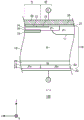
图1是示出本实施方式的半导体装置100的上表面的一例的图。
图2A是示出半导体装置100的上表面的一例的放大图。
图2B是示出图2A中的a-a’截面的图。
图2C是示出图2A中的b-b’截面的图。
图2D是示出图2A中的c-c’截面的图。
图2E是示出图2A中的a-a’截面的另一例的图。
图2F是示出图2A中的a-a’截面的另一例的图。
图3A是示出沟槽底部区Rp和电子通过区Rn的配置的一例的图。
图3B是示出图3A中的d-d’截面的图。
图4A是示出沟槽底部区Rp和电子通过区Rn的配置的一例的图。
图4B是示出图4A中的e-e’截面的图。
图5A是示出沟槽底部区Rp和电子通过区Rn的配置的一例的图。
图5B是示出图5A中的f-f’截面的图。
符号说明
10…半导体基板、11…阱区、12…发射区、14…基区、15…接触区、16…蓄积区、17…插塞区、18…漂移区、20…缓冲区、21…正面、22…集电区、23…背面、24…集电电极、25…连接部、29…直线部分、30…虚设沟槽部、31…前端部、32…虚设绝缘膜、34…虚设导电部、38…层间绝缘膜、39…直线部分、40…栅极沟槽部、41…前端部、42…栅极绝缘膜、44…栅极导电部、48…栅极流道、49…接触孔、50…栅极金属层、52…发射电极、54…接触孔、56…接触孔、60…台面部、61…台面部、70…晶体管部、75…沟槽底部、77…电子通过部、80…二极管部、82…阴极区、92…保护环、100…半导体装置、102…端边、160…有源部、190…耐压结构部
具体实施方式
以下,虽然通过发明的实施方式对本发明进行说明,但是以下的实施方式并不限定权利要求所涉及的发明。另外,实施方式中所说明的特征的全部组合未必是发明的技术方案所必须的。
在本说明书中,将与半导体基板的深度方向平行的方向的一侧称为“上”或“正”,将另一侧称为“下”或“背”。将基板、层或其他部件的两个主面中的一个面称为正面,将另一个面称为背面。“上”、“下”的方向并不限于重力方向或半导体装置实际安装时的方向。
在本说明书中,有时使用X轴、Y轴和Z轴的直角坐标轴来说明技术事项。直角坐标轴仅仅确定构成要素的相对位置,并不限定特定的方向。例如,Z轴并不限定地表示相对于地面的高度方向。应予说明,+Z轴方向和-Z轴方向是彼此相反的方向。在不记载正负而记载为Z轴方向的情况下,是指与+Z轴和Z轴平行的方向。
在本说明书中,将与半导体基板的正面和背面平行的正交轴设为X轴和Y轴。另外,将与半导体基板的正面和背面垂直的轴设为Z轴。在本说明书中,有时将Z轴的方向称为深度方向。另外,在本说明书中,有时将包括X轴和Y轴在内的与半导体基板的正面和背面平行的方向称为水平方向。
在本说明书中,在称为“相同”或“相等”的情况下,也可以包括具有由制造偏差等引起的误差的情况。该误差例如在10%以内。
在本说明书中,将掺杂有杂质的掺杂区的导电型设为P型或N型而进行说明。在本说明书中,杂质有时特别是指N型的施主或P型的受主中的任一个,有时记载为掺杂剂。在本说明书中,掺杂是指向半导体基板导入施主或受主,形成为呈现N型的导电型的半导体或呈现P型的导电型的半导体。
在本说明书中,掺杂浓度是指热平衡状态下的施主的浓度或受主的浓度。在本说明书中,净掺杂浓度是指,将施主浓度设为正离子的浓度并将受主浓度设为负离子的浓度而包含电荷的极性在内相加而得的实质的浓度。作为一例,如果将施主浓度设为ND,并将受主浓度设为NA,则任意位置处的实质的净掺杂浓度成为ND-NA。
施主具有向半导体供给电子的功能。受主具有从半导体获取电子的功能。施主和受主不限于杂质本身。例如,存在于半导体中的空位(V)、氧(O)以及氢(H)结合所得的VOH缺陷作为供给电子的施主而发挥功能。
在本说明书中,在记载为P+型或N+型的情况下,意味着掺杂浓度高于P型或N型的掺杂浓度,在记载为P-型或N-型的情况下,意味着掺杂浓度低于P型或N型的掺杂浓度。另外,在本说明书中,在记载为P++型或N++型的情况下,意味着掺杂浓度高于P+型或N+型的掺杂浓度。
在本说明书中,化学浓度是指不依赖于电活化的状态而测定的杂质的浓度。化学浓度能够通过例如二次离子质谱法(SIMS)来计测。上述净掺杂浓度可以通过电压-电容测定法(CV法)来测定。另外,可以将通过扩展电阻测定法(SR法)计测出的载流子密度作为净掺杂浓度。通过CV法或SR法计测出的载流子密度可以作为净掺杂浓度。另外,在N型的区域中,施主浓度远远大于受主浓度,因此也可以将该区域中的载流子浓度设为施主浓度。同样地,在P型的区域中,也可以将该区域中的载流子浓度设为受主浓度。
另外,在施主、受主或净掺杂的浓度分布具有峰的情况下,可以将该峰值作为该区域中的施主、受主或净掺杂的浓度。在施主、受主或净掺杂的浓度几乎均匀的情况下等,可以将该区域中的施主、受主或净掺杂的浓度的平均值作为施主、受主或净掺杂的浓度。
通过SR法计测出的载流子浓度也可以低于施主或受主的浓度。在测定扩展电阻时电流流通的范围内,有时半导体基板的载流子迁移率低于结晶状态的载流子迁移率的值。由于晶格缺陷等引起的晶体结构的紊乱(无序)而使载流子散乱,从而产生载流子迁移率的下降。
根据利用CV法或SR法计测的载流子浓度而计算出的施主或受主的浓度可以低于表示施主或受主的元素的化学浓度。作为一例,在硅的半导体中成为施主的磷或砷的施主浓度或者成为受主的硼(boron)的受主浓度为它们的化学浓度的99%左右。另一方面,在硅的半导体中成为施主的氢的施主浓度为氢的化学浓度的0.1%至10%左右。
图1是示出本实施方式的半导体装置100的上表面的一例的图。在图1中,示出将各部件投影到半导体基板10的正面而得的位置。在图1中,仅示出半导体装置100的一部分的部件,省略另一部分的部件。
半导体装置100具备半导体基板10。半导体基板10在俯视时具有端边102。在本说明书中简称为俯视的情况下,是指从半导体基板10的正面侧观察。本例的半导体基板10具有在俯视时彼此对置的两组端边102。在图1中,X轴和Y轴与任一个端边102平行。另外,Z轴与半导体基板10的正面垂直。
在半导体基板10设置有有源部160。有源部160是在半导体装置100动作的情况下主电流沿深度方向在半导体基板10的正面与背面之间流通的区域。在有源部160的上方设置有发射电极,但在图1中省略。
在有源部160设置有包括IGBT等晶体管元件的晶体管部70和包括续流二极管(FWD)等二极管元件的二极管部80中的至少一方。在图1的例子中,晶体管部70和二极管部80沿着半导体基板10的正面的预定的排列方向(在本例中为X轴方向)交替地配置。在另一例中,在有源部160也可以仅设置有晶体管部70。
在图1中,对配置有晶体管部70的区域标注符号“I”,对配置有二极管部80的区域标注符号“F”。在本说明书中,有时将在俯视时与排列方向垂直的方向称为延伸方向(在图1中为Y轴方向)。晶体管部70和二极管部80可以分别在延伸方向上具有长边。即,晶体管部70的Y轴方向上的长度大于晶体管部70的X轴方向上的宽度。同样地,二极管部80的Y轴方向上的长度大于X轴方向上的宽度。晶体管部70和二极管部80的延伸方向与后述的各沟槽部的长边方向可以相同。
晶体管部70在与半导体基板10的背面相接的区域具有P+型的集电区。二极管部80在与半导体基板10的背面相接的区域具有N+型的阴极区。在本说明书中,将设置有集电区的区域称为晶体管部70。即,晶体管部70是在俯视时与集电区重叠的区域。
在半导体基板10的背面,在除集电区以外的区域可以设置有N+型的阴极区。在本说明书中,在将晶体管部70沿Y轴方向延长到后述的栅极流道的延长区的下表面设置有阴极区。在本说明书中,延长区包含于二极管部80。另外,晶体管部70在半导体基板10的正面侧周期性地配置有N型的发射区、P型的基区、以及具有栅极导电部和栅极绝缘膜的栅极结构。
半导体装置100在半导体基板10的上方可以具有一个以上的焊盘。作为一例,图1所示的半导体装置100具有栅极焊盘G,但这仅仅是例示。半导体装置100也可以具有阳极焊盘、阴极焊盘以及电流检测焊盘等焊盘。各焊盘配置于端边102的附近。端边102的附近是指俯视时的端边102与发射电极之间的区域。在半导体装置100实际安装时,各焊盘可以经由引线等布线与外部的电路连接。
在栅极焊盘G施加栅极电位。栅极焊盘G与有源部160的栅极沟槽部的导电部电连接。半导体装置100具备将栅极焊盘G与栅极沟槽部电连接的栅极流道48。
栅极流道48在俯视时配置在有源部160与半导体基板10的端边102之间。本例的栅极流道48在俯视时包围有源部160。也可以将在俯视时被栅极流道48包围的区域作为有源部160。
栅极流道48配置在半导体基板10的上方。本例的栅极流道48可以由掺杂有杂质的多晶硅等形成。栅极流道48与隔着栅极绝缘膜设置在栅极沟槽部的内部的栅极导电部电连接。
本例的半导体装置100具备设置在有源部160的外周的耐压结构部190。本例的耐压结构部190配置在栅极流道48与端边102之间。耐压结构部190缓解半导体基板10的正面侧的电场集中。
耐压结构部190可以具有保护环92。保护环92是与半导体基板10的正面相接的P型的区域。应予说明,本例的耐压结构部190具有多个保护环92,但在图1中省略而仅示出一个保护环92。通过设置多个保护环92,从而能够使有源部160的上表面侧的耗尽层向外侧延伸,能够提高半导体装置100的耐压。耐压结构部190还可以具备包围有源部160而设置为环状的场板和降低表面电场中的至少一个。
另外,半导体装置100也可以具备由多晶硅等形成的PN结二极管即未图示的温度感测部和/或与设置在有源部160的晶体管部进行同样的动作的未图示的电流检测部。
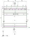
图2A是示出半导体装置100的上表面的一例的放大图。图2A示出图1所示的区域A即有源部160与耐压结构部190的边界附近。半导体装置100具备半导体基板,该半导体基板具有包括IGBT等晶体管元件的晶体管部70和包括续流二极管(FWD)等二极管元件的二极管部80。
本例的晶体管部70和二极管部80沿着排列方向(在本例中为X轴方向)交替地配置。二极管部80在俯视时设置在靠近耐压结构部190的晶体管部70与耐压结构部190之间。即,在有源部160的最外侧配置有二极管部80。应予说明,在本说明书中,在仅称为“内侧”和“外侧”的情况下,朝向半导体装置100的中心的方向是指内侧,远离半导体装置100的中心的方向是指外侧。
本例的半导体装置100具备设置在半导体基板的正面侧的栅极沟槽部40、虚设沟槽部30、阱区11、发射区12、基区14以及接触区15。栅极沟槽部40和虚设沟槽部30分别是沟槽部的一例。
另外,本例的半导体装置100具备设置在半导体基板的正面的上方的栅极金属层50和发射电极52。栅极金属层50和发射电极52彼此分离地设置。栅极金属层50与发射电极52电绝缘。
在发射电极52与半导体基板的正面之间、以及栅极金属层50与半导体基板的正面之间设置有层间绝缘膜,但是在图2A中进行省略。在本例的层间绝缘膜,以贯通该层间绝缘膜的方式设置有接触孔49、接触孔54以及接触孔56。在图2A中,对各个接触孔标注斜线的阴影。
发射电极52设置在栅极沟槽部40、虚设沟槽部30、阱区11、发射区12、基区14以及接触区15的上方。发射电极52通过接触孔54与半导体基板的正面的发射区12、基区14以及接触区15电连接。
另外,发射电极52通过接触孔56与虚设沟槽部30内的虚设导电部连接。在发射电极52与虚设导电部之间可以设置有由掺杂有杂质的多晶硅等具有导电性的材料形成的连接部25。连接部25隔着层间绝缘膜和虚设沟槽部30的虚设绝缘膜等绝缘膜设置在半导体基板的正面。
栅极金属层50通过接触孔49与栅极流道48电连接。栅极流道48可以由掺杂有杂质的多晶硅等形成。栅极流道48在半导体基板的正面与栅极沟槽部40内的栅极导电部连接。栅极流道48不与虚设沟槽部30内的虚设导电部和发射电极52电连接。
栅极流道48与发射电极52通过层间绝缘膜和氧化膜等绝缘物而电分离。本例的栅极流道48从接触孔49的下方设置到栅极沟槽部40的前端部。在栅极沟槽部40的前端部,栅极导电部在半导体基板的正面露出,并与栅极流道48连接。
发射电极52和栅极金属层50由包含金属的导电性材料形成。例如,由铝或以铝为主要成分的合金(例如,铝-硅合金等)形成。各电极可以在由铝等形成的区域的下层具有由钛、钛化合物等形成的阻挡金属。
各电极也可以在接触孔内具有由钨等形成的插塞。对于插塞而言,可以在与半导体基板相接的一侧具有阻挡金属,以与阻挡金属相接的方式埋入钨,在钨上形成铝等。
应予说明,插塞设置在与接触区15或基区14相接的接触孔。另外,在插塞的接触孔之下形成P++型的插塞区,该插塞区的掺杂浓度高于接触区15的掺杂浓度。这能够改善阻挡金属与接触区15之间的接触电阻。另外,插塞区的深度为大致0.1μm以下,具有比接触区15的深度小10%以下的区域。
插塞区具有以下特征。在晶体管部70动作中,通过改善接触电阻而提高闩锁耐量。另一方面,在二极管部80动作中,在没有插塞区的情况下,阻挡金属与基区14之间的接触电阻高,导通损耗、开关损耗上升,但是通过设置插塞区,而能够抑制导通损耗、开关损耗的上升。
阱区11与栅极流道48重叠,在有源部160的外周延伸,并在俯视时设置为环状。阱区11在不与栅极流道48重叠的范围内也以预定的宽度延伸,并在俯视时设置为环状。本例的阱区11从接触孔54的Y轴方向的端部向栅极流道48侧分离而设置。阱区11是掺杂浓度高于基区14的掺杂浓度的第二导电型的区域。栅极流道48与阱区11电绝缘。
本例的基区14为P-型,阱区11为P+型。另外,阱区11从半导体基板的正面形成至比基区14的下端更深的位置。基区14在晶体管部70和二极管部80中与阱区11相接地设置。因此,阱区11与发射电极52电连接。
晶体管部70和二极管部80分别具有在排列方向上排列为多排的沟槽部。在本例的晶体管部70,沿着排列方向设置有一个以上的栅极沟槽部40。在本例的二极管部80,沿着排列方向设置有多个虚设沟槽部30。在本例的二极管部80不设置栅极沟槽部40。
本例的栅极沟槽部40可以具有沿着与排列方向垂直的延伸方向延伸的两个直线部分39(沿着延伸方向呈直线状的沟槽的部分)以及连接两个直线部分39的前端部41。
前端部41的至少一部分可以在俯视时设置为曲线状。通过前端部41将两个直线部分39的Y轴方向上的端部彼此与栅极流道48连接,从而作为向栅极沟槽部40的栅电极而发挥功能。另一方面,通过将前端部41设为曲线状,从而与在直线部分39完结相比更能够缓解端部处的电场集中。
在另一例中,晶体管部70可以沿着排列方向交替地设置有一个以上的栅极沟槽部40和一个以上的虚设沟槽部30。在晶体管部70中,虚设沟槽部30设置在栅极沟槽部40的各个直线部分39之间。在各个直线部分39之间可以设置有一条虚设沟槽部30,也可以设置有多条虚设沟槽部30。
另外,在各个直线部分39之间,可以不设置虚设沟槽部30,还可以设置栅极沟槽部40。通过这样的结构,能够增大来自发射区12的电子电流,因此导通电压降低。
虚设沟槽部30可以具有沿延伸方向延伸的直线形状,也可以与栅极沟槽部40同样地具有直线部分29和前端部31。虽然图2A所示的半导体装置100仅排列有具有前端部31的虚设沟槽部30,但是在另一例中,半导体装置100也可以包括不具有前端部31的直线形状的虚设沟槽部30。
阱区11的扩散深度可以比栅极沟槽部40和虚设沟槽部30的深度更深。栅极沟槽部40和虚设沟槽部30的Y轴方向的端部在俯视时设置在阱区11。即,在各沟槽部的Y轴方向的端部,各沟槽部的深度方向的底部被阱区11覆盖。另外,设置在X轴方向的端部的沟槽部也可以被阱区11覆盖。由此,能够缓解各沟槽部的该底部处的电场集中。
在排列方向上,在各沟槽部之间设置有台面部。台面部是指在半导体基板的内部被沟槽部夹持的区域。作为一例,台面部的深度位置是从半导体基板的正面起到沟槽部的下端为止的位置。
本例的台面部被在X轴方向上相邻的沟槽部夹持,在半导体基板的正面沿着沟槽在延伸方向(Y轴方向)上延伸而设置。在图2B中,如后述的那样,在本例中,在晶体管部70设置有台面部60,在二极管部80设置有台面部61。在本说明书中,在仅称为台面部的情况下,分别是指台面部60和台面部61。
在各个台面部设置有基区14。在各个台面部,在俯视时被基区14夹持的区域可以设置有第一导电型的发射区12和第二导电型的接触区15中的至少一方。本例的发射区12为N+型,接触区15为P+型。发射区12和接触区15在深度方向上可以设置在基区14与半导体基板的正面之间。
晶体管部70的台面部具有在半导体基板的正面露出的发射区12。发射区12与栅极沟槽部40相接而设置。在与栅极沟槽部40相接的台面部设置有在半导体基板的正面露出的接触区15。
台面部中的接触区15和发射区12分别从X轴方向上的一个沟槽部设置到另一个沟槽部。作为一例,台面部的接触区15和发射区12沿着沟槽部的延伸方向(Y轴方向)交替地配置。
在另一例中,台面部的接触区15和发射区12可以沿着沟槽部的延伸方向(Y轴方向)设置为条纹状。例如,在与沟槽部相接的区域设置有发射区12,在被发射区12夹持的区域设置有接触区15。
在二极管部80的台面部不设置发射区12。在二极管部80的台面部的上表面可以设置有基区14。基区14可以配置于二极管部80的整个台面部。
在各个台面部的上方设置有接触孔54。接触孔54在其延伸方向(Y轴方向)上配置于被基区14夹持的区域。本例的接触孔54设置在接触区15、基区14以及发射区12的各区域的上方。接触孔54可以配置在台面部的排列方向(X轴方向)上的中央。
在二极管部80中,在与半导体基板的背面相邻的区域设置有N+型的阴极区82。在半导体基板的背面,在不设置阴极区82的区域可以设置有P+型的集电区22。在图2A中,利用虚线表示阴极区82与集电区22的边界。在耐压结构部190中,也可以在半导体基板的背面侧设置N+型的阴极区82。
图2B是示出图2A中的a-a’截面的图。a-a’截面是通过接触区15、基区14、以及栅极沟槽部40和虚设沟槽部30的XZ面。本例的半导体装置100在a-a’截面具有半导体基板10、层间绝缘膜38、发射电极52和集电电极24。
层间绝缘膜38设置在半导体基板10的正面21。层间绝缘膜38是添加有硼或磷等杂质的硅酸盐玻璃等绝缘膜。层间绝缘膜38可以与正面21相接,也可以在层间绝缘膜38与正面21之间设置有氧化膜等其他膜。在层间绝缘膜38设置有在图2A中说明的接触孔54。
发射电极52设置在半导体基板10的正面21和层间绝缘膜38的上表面。发射电极52通过层间绝缘膜38的接触孔54而与正面21电连接。在接触孔54的内部可以设置有钨(W)等的插塞区17。集电电极24设置在半导体基板10的背面23。发射电极52和集电电极24由包含金属的材料或它们的层叠膜形成。
半导体基板10可以是硅基板,也可以是碳化硅基板,还可以是氮化镓等氮化物半导体基板等。本例的半导体基板10为硅基板。
半导体基板10具有第一导电型的漂移区18。本例的漂移区18为N-型。漂移区18可以是在半导体基板10中不设置其他掺杂区而残留的区域。
在晶体管部70中,在漂移区18的上方,可以沿Z轴方向设置有一个以上的蓄积区16。蓄积区16是以比漂移区18的浓度更高的方式蓄积了与漂移区18相同的掺杂剂而得的区域。蓄积区16的掺杂浓度高于漂移区18的掺杂浓度。
本例的蓄积区16为N型。蓄积区16在晶体管部70中可以设置在基区14与后述的沟槽底部75之间。蓄积区16可以仅设置于晶体管部70,也可以设置于晶体管部70和二极管部80这两者。通过设置蓄积区16,从而能够提高载流子的注入促进效果(IE效果),降低导通电压。
在晶体管部70中,在基区14的上方,以与正面21相接的方式设置有发射区12。发射区12与栅极沟槽部40相接地设置。发射区12的掺杂浓度高于漂移区18的掺杂浓度。作为一例,发射区12的掺杂剂是砷(As)、磷(P)、锑(Sb)等。
在二极管部80设置有在正面21露出的基区14。二极管部80的基区14作为阳极而动作。
在漂移区18的下方可以设置有第一导电型的缓冲区20。本例的缓冲区20为N型。缓冲区20的掺杂浓度高于漂移区18的掺杂浓度。缓冲区20可以作为防止从基区14的下表面侧扩展的耗尽层到达集电区22和阴极区82的场截止层而发挥功能。
在晶体管部70中,在缓冲区20的下方设置有集电区22。集电区22可以在背面23与阴极区82相接地设置。
在二极管部80中,在缓冲区20的下方设置有阴极区82。阴极区82可以设置在与晶体管部70的集电区22相同的深度。二极管部80可以作为在晶体管部70关断时流过反向导通的回流电流的续流二极管(FWD)而发挥功能。
在半导体基板10设置有栅极沟槽部40和虚设沟槽部30。栅极沟槽部40和虚设沟槽部30以从正面21贯通基区14和蓄积区16而到达漂移区18的方式设置。沟槽部贯通掺杂区并不限于以形成掺杂区之后形成沟槽部的顺序进行制造。在形成沟槽部之后,在沟槽部之间形成掺杂区的情况也包括在沟槽部贯通掺杂区的情况中。
栅极沟槽部40具有设置在正面21的栅极沟槽、栅极绝缘膜42以及栅极导电部44。栅极绝缘膜42覆盖栅极沟槽的内壁而设置。栅极绝缘膜42可以由氧化膜或氮化膜形成。栅极导电部44以在栅极沟槽的内部将比栅极绝缘膜42靠内侧的部分填埋的方式设置。栅极导电部44的上表面可以位于与正面21相同的XY平面内。栅极绝缘膜42将栅极导电部44与半导体基板10绝缘。栅极导电部44由掺杂有杂质的多晶硅等形成。
栅极导电部44可以在深度方向上设置得比基区14更长。栅极沟槽部40在正面21被层间绝缘膜38覆盖。如果对栅极导电部44施加预定的电压,则在基区14中的与栅极沟槽相接的界面的表层形成由电子的反型层形成的沟道。
虚设沟槽部30在XZ截面可以具有与栅极沟槽部40相同的结构。虚设沟槽部30具有设置在正面21的虚设沟槽、虚设绝缘膜32以及虚设导电部34。虚设绝缘膜32覆盖虚设沟槽的内壁而设置。虚设绝缘膜32可以由氧化膜或氮化膜形成。虚设导电部34以在虚设沟槽的内部将比虚设绝缘膜32靠内侧的部分填埋的方式设置。虚设导电部34的上表面可以位于与正面21相同的XY平面内。虚设绝缘膜32将虚设导电部34与半导体基板10绝缘。虚设导电部34可以由与栅极导电部44相同的材料形成。
本例的栅极沟槽部40和虚设沟槽部30在正面21被层间绝缘膜38覆盖。应予说明,虚设沟槽部30和栅极沟槽部40的底部可以是向下侧凸出的曲面状(在截面中为曲线状)。
晶体管部70具有设置在沟槽部的下端的P型的沟槽底部75。本例的沟槽底部75设置在比蓄积区16靠下方的位置。在半导体基板10的深度方向上,沟槽底部75的下端可以位于比栅极沟槽部40的底部靠下方的位置。换言之,沟槽底部75可以覆盖栅极沟槽部40的底部。
沟槽底部75的掺杂浓度高于漂移区18的掺杂浓度且低于基区14的掺杂浓度。沟槽底部75的掺杂浓度为1E12cm-3以上且1E13cm-3以下。
在图2B中,沟槽底部75的X轴方向正侧(二极管部80侧)的端部与阴极区82和集电区22的边界一致,但也可以比所述阴极区82和集电区22的边界更向二极管部80侧延伸,还可以后退到晶体管部70内。
沟槽底部75可以是电浮置的浮置层。在本说明书中,浮置层是指不与发射电极52等任何电极电连接的层。通过设置沟槽底部75,从而晶体管部70的导通特性提高。另外,通过设置沟槽底部75,从而缓解栅极沟槽部40的底部处的电场集中,提高雪崩耐量。
图2C是示出图2A中的b-b’截面的图。b-b’截面是在有源部160的Y轴负侧端部附近,通过设置于二极管部80的基区14和接触区15的YZ面。
在本例中,在有源部160的最外侧设置有二极管部80。在二极管部80中,在半导体基板10的正面21设置有接触区15。另外,在二极管部80中,在接触区15的Y轴方向外侧,基区14在半导体基板10的正面21露出。即,在俯视时,在二极管部80中,在Y轴方向上,接触区15被基区14夹持。
在有源部160的Y轴负侧端部附近设置有阱区11。阱区11的扩散深度比基区14深。阱区11可以以局部地覆盖基区14的底部的方式沿Y轴方向延伸。
图2D是示出图2A中的c-c’截面的图。c-c’截面是在有源部160的Y轴负侧端部附近,通过设置于晶体管部70的发射区12、基区14以及接触区15的YZ面。另外,c-c’截面通过将晶体管部70沿Y轴方向延长而成的延长区。在延长区的下表面设置有阴极区。即,在俯视时,晶体管部70在Y轴方向上被二极管部80夹持。
在晶体管部70中,在半导体基板10的正面21设置有发射区12和接触区15。另外,在晶体管部70中,在接触区15的Y轴方向外侧,基区14在半导体基板10的正面21露出。即,在俯视时,在晶体管部70中,在Y轴方向上,发射区12和接触区15被基区14夹持。
在晶体管部70中,在漂移区18的上方设置有蓄积区16和沟槽底部75。沟槽底部75设置在比蓄积区16靠下方的位置。沟槽底部75可以与蓄积区16的下表面相接地设置。或者,如后所述,沟槽底部75也可以与蓄积区16分离,即,以使漂移区18介于蓄积区16与沟槽底部75之间的方式设置。
图2E是示出图2A中的a-a’截面的另一例的图。a-a’截面与图2B同样地是通过接触区15、基区14、以及栅极沟槽部40和虚设沟槽部30的XZ面。本例的半导体装置100在a-a’截面具有半导体基板10、层间绝缘膜38、发射电极52以及集电电极24。
晶体管部70的设置在沟槽部的下端的沟槽底部75与图2B的沟槽底部75在半导体基板10的深度方向上的厚度比蓄积区16薄这一点与图2B不同。
本例的沟槽底部75的下端位于比栅极沟槽部40的底部靠下方的位置,并覆盖栅极沟槽部40的底部。
沟槽底部75可以是电浮置的浮置层。
在图2E中,沟槽底部75的X轴方向正侧(二极管部80侧)的端部与阴极区82和集电区22的边界一致,但也可以比所述阴极区82和集电区22的边界更向二极管部80侧延伸,还可以后退到晶体管部70内。本例能够得到与图2B同样的效果。
图2F是示出图2A中的a-a’截面的另一例的图。a-a’截面是与图2B同样地通过接触区15、基区14、以及栅极沟槽部40和虚设沟槽部30的XZ面。本例的半导体装置100在a-a’截面具有半导体基板10、层间绝缘膜38、发射电极52以及集电电极24。
图2G的沟槽底部75与蓄积区16分离,即,以使漂移区18介于蓄积区16与沟槽底部75之间的方式设置这一点与图2B、图2F的不同。
在半导体基板10的深度方向上,沟槽底部75的厚度可以比蓄积区16的厚度、或者蓄积区16与沟槽底部75之间的漂移区18的厚度薄。
在图2F中,沟槽底部75的X轴方向正侧(二极管部80侧)的端部与阴极区82和集电区22的边界一致,但也可以比阴极区82和集电区22的边界更向二极管部80侧延伸,还可以后退到晶体管部70内。本例能够得到与图2B同样的效果。
图3A是示出沟槽底部区Rp和电子通过区Rn的配置的一例的图。图3B是示出图3A中的d-d’截面的图。本例的沟槽底部75在晶体管部70间断地设置。晶体管部70在与沟槽底部75相同的Z轴方向位置具有设置在沟槽底部75之间的电子通过部77。在图3B中,虽然利用阴影表示电子通过部77的范围,但是电子通过部77是与漂移区18相同的N型的区域,也可以是漂移区18的一部分。
在本说明书中,将在俯视时与沟槽底部75对应的区域称为沟槽底部区Rp,将在俯视时与电子通过部77对应的区域称为电子通过区Rn。本例的晶体管部70在俯视时具有未设置沟槽底部75的电子通过区Rn。
电子通过区Rn被设置为在X轴方向上从沟槽部延伸至相邻的沟槽部。即,如图3A所示,电子通过区Rn被设置为在X轴方向上遍及台面部而延伸。应予说明,在图3A中,作为沟槽部,仅示出栅极沟槽部40,但不限于此。电子通过区Rn被设置为在X轴方向上遍及多个虚设沟槽部30和栅极沟槽部40中的相邻的两者之间的台面部而延伸。
电子通过区Rn可以在X轴方向上越过多个沟槽部而延伸。即,电子通过区Rn可以在俯视时与发射区12平行地延伸。
在本例中,在电子通过区Rn的台面部不设置发射区12。即,如图3B所示,在电子通过部77的上方不设置发射区12,在发射区12的下方设置有沟槽底部75。如图3A所示,电子通过区Rn以在俯视时Y轴方向端部位于接触区15内的方式设置。
如果沟槽底部区Rp设置于整个晶体管部70,则在晶体管部70导通时,瞬态电阻一直增大到沟槽底部75的电位上升为止,因此导通电阻有可能恶化。
在本例中,在晶体管部70导通时,来自发射区12的电子首先通过电子通过部7而前往集电区22。之后,如果在沟槽底部75蓄积有来自集电区22的空穴,则电子也通过沟槽底部75,达到导通。这样,通过晶体管部70具有电子通过区Rn,从而抑制晶体管部70导通时的瞬态电阻的增大,改善了导通电阻。
在电子通过部77中,由于电流集中所以容易发生雪崩。然而,在本例中,通过在电子通过区Rn的台面部不设置发射区12,能够降低在电子通过部77发生闩锁的可能性。这样,在本例中,通过在发射区12的下方设置沟槽底部75,从而能够改善导通特性,并且改善导通电阻。
图4A是示出沟槽底部区Rp和电子通过区Rn的配置的一例的图。图4B是示出图4A中的e-e’截面的图。与图3A和图3B同样地,本例的沟槽底部75在晶体管部70间断地设置,晶体管部70在与沟槽底部75相同的Z轴方向位置具有设置于沟槽底部75之间的电子通过部77。
与图3A和图3B同样地,本例的电子通过区Rn被设置为在X轴方向上从沟槽部延伸至相邻的沟槽部。即,电子通过区Rn被设置为在X轴方向上遍及台面部而延伸。另外,电子通过区Rn可以在X轴方向上越过多个沟槽部而延伸。即,电子通过区Rn可以在俯视时与沟槽部正交地延伸。
与图3A和图3B不同,在本例的电子通过区Rn至少设置有发射区12。即,在任一发射区12的下方设置有电子通过部77。由此,在晶体管部70导通时,来自发射区12的电子能够可靠地通过电子通过部77。这样,通过晶体管部70具有电子通过区Rn,从而抑制晶体管部70导通时的瞬态电阻的增大,改善了导通电阻。
图5A是示出沟槽底部区Rp和电子通过区Rn的配置的一例的图。图5B是示出图5A中的f-f’截面的图。与图3A~图4B同样地,本例的沟槽底部75在晶体管部70间断地设置,晶体管部70在与沟槽底部75相同的Z轴方向位置具有设置在沟槽底部75之间的电子通过部77。
与图3A~图4B不同,在本例中,沟槽底部区Rp和电子通过区Rn在X轴方向上交替地设置。即,如图5A所示,沟槽底部区Rp和电子通过区Rn在俯视时与栅极沟槽部40平行地延伸而交替地设置。
在电子通过区Rn可以至少设置有栅极沟槽部40。即,在任一栅极沟槽部40的下方设置有电子通过部77。如果在设置于电子通过区Rn的栅极沟槽部40形成有沟道,则来自沟道的电子能够可靠地通过下方的电子通过部77。这样,通过晶体管部70具有电子通过区Rn,从而抑制晶体管部70导通时的瞬态电阻的增大,改善了导通电阻。
以上,虽然利用实施方式对本发明进行了说明,但是本发明的技术范围并不限定于上述实施方式所记载的范围。能够对上述实施方式施加各种变更或改良,这对于本领域技术人员而言是显而易见的。根据权利要求书的记载可知,施加了这样的变更或改良的方式也能够包含在本发明的技术范围内。
需要注意的是,权利要求书、说明书及附图中所示的装置、系统、程序及方法中的动作、过程、步骤以及阶段等各处理的执行顺序只要没有特别明示“早于”、“预先”等,另外,未在后续处理中使用之前的处理结果,,则能够以任意的顺序实现。关于权利要求书、说明书及附图中的动作流程,即使为了方便而使用“首先”、“接下来”等进行了说明,也并不意味着必须按照该顺序实施。
Claims (13)
1.一种半导体装置,其特征在于,具备晶体管部,
所述半导体装置具备:
第一导电型的漂移区,其设置于半导体基板;
多个沟槽部,其从所述半导体基板的正面延伸至所述漂移区;
第一导电型的发射区,其设置为在所述半导体基板的正面,从所述多个沟槽部中的沟槽部延伸至相邻的沟槽部,并且掺杂浓度高于所述漂移区的掺杂浓度;以及
第二导电型的沟槽底部,其设置于所述沟槽部的下端,
所述晶体管部在俯视时具有不设置所述沟槽底部的电子通过区。
2.根据权利要求1所述的半导体装置,其特征在于,
所述电子通过区设置为在沟槽排列方向上从所述多个沟槽部中的沟槽部延伸至相邻的沟槽部。
3.根据权利要求2所述的半导体装置,其特征在于,
所述电子通过区在沟槽排列方向上越过多个沟槽部而延伸。
4.根据权利要求1至3中任一项所述的半导体装置,其特征在于,
在所述电子通过区的台面部不设置所述发射区。
5.根据权利要求1至4中任一项所述的半导体装置,其特征在于,
在所述发射区的下方设置有所述沟槽底部。
6.根据权利要求1至5中任一项所述的半导体装置,其特征在于,
所述半导体装置还具备设置在所述半导体基板的正面的第二导电型的接触区,
所述电子通过区以在俯视时沟槽延伸方向端部位于所述接触区内的方式设置。
7.根据权利要求1至3中任一项所述的半导体装置,其特征在于,
在所述电子通过区至少设置有所述发射区。
8.根据权利要求1至3中任一项所述的半导体装置,其特征在于,
所述晶体管部在俯视时具有形成有所述沟槽底部的沟槽底部区,
所述沟槽底部区和所述电子通过区在沟槽排列方向上交替地设置。
9.根据权利要求8所述的半导体装置,其特征在于,在所述电子通过区至少设置有被施加栅极电压的栅极沟槽部。
10.根据权利要求1至9中任一项所述的半导体装置,其特征在于,
所述沟槽底部电浮置。
11.根据权利要求1至10中任一项所述的半导体装置,其特征在于,所述沟槽底部的掺杂浓度为1E12cm-3以上且1E13cm-3以下。
12.根据权利要求1至11中任一项所述的半导体装置,其特征在于,所述半导体装置还具备设置在所述漂移区的上方的第一导电型的蓄积区。
13.根据权利要求12所述的半导体装置,其特征在于,
所述漂移区介于所述蓄积区与所述沟槽底部之间。
Applications Claiming Priority (3)
| Application Number | Priority Date | Filing Date | Title |
|---|---|---|---|
| JP2021-080625 | 2021-05-11 | ||
| JP2021080625 | 2021-05-11 | ||
| PCT/JP2021/045159 WO2022239285A1 (ja) | 2021-05-11 | 2021-12-08 | 半導体装置 |
Publications (2)
| Publication Number | Publication Date |
|---|---|
| CN116349006A true CN116349006A (zh) | 2023-06-27 |
| CN116349006A9 CN116349006A9 (zh) | 2023-07-25 |
Family
ID=84028093
Family Applications (1)
| Application Number | Title | Priority Date | Filing Date |
|---|---|---|---|
| CN202180072875.0A Pending CN116349006A (zh) | 2021-05-11 | 2021-12-08 | 半导体装置 |
Country Status (5)
| Country | Link |
|---|---|
| US (1) | US20230261095A1 (zh) |
| JP (1) | JPWO2022239285A1 (zh) |
| CN (1) | CN116349006A (zh) |
| DE (1) | DE112021004603T5 (zh) |
| WO (1) | WO2022239285A1 (zh) |
Cited By (1)
| Publication number | Priority date | Publication date | Assignee | Title |
|---|---|---|---|---|
| CN117577669A (zh) * | 2023-11-16 | 2024-02-20 | 浙江旺荣半导体有限公司 | 一种逆导型绝缘栅双极晶体管 |
Families Citing this family (1)
| Publication number | Priority date | Publication date | Assignee | Title |
|---|---|---|---|---|
| CN117561611A (zh) * | 2022-01-20 | 2024-02-13 | 富士电机株式会社 | 半导体装置 |
Family Cites Families (5)
| Publication number | Priority date | Publication date | Assignee | Title |
|---|---|---|---|---|
| JP5396953B2 (ja) * | 2009-03-19 | 2014-01-22 | 株式会社デンソー | 炭化珪素半導体装置およびその製造方法 |
| JP5013436B2 (ja) * | 2009-06-04 | 2012-08-29 | 三菱電機株式会社 | 電力用半導体装置 |
| DE102013213026A1 (de) * | 2013-07-03 | 2015-01-08 | Robert Bosch Gmbh | Feldplatten-Trench-FET sowie ein Halbleiterbauelement |
| DE102017124871B4 (de) | 2017-10-24 | 2021-06-17 | Infineon Technologies Ag | Leistungshalbleiter-Vorrichtung und Verfahren zum Herstellen einer Leistungshalbleiter-Vorrichtung |
| JP7404702B2 (ja) * | 2019-08-09 | 2023-12-26 | 富士電機株式会社 | 半導体装置 |
-
2021
- 2021-12-08 WO PCT/JP2021/045159 patent/WO2022239285A1/ja active Application Filing
- 2021-12-08 JP JP2023520757A patent/JPWO2022239285A1/ja active Pending
- 2021-12-08 DE DE112021004603.9T patent/DE112021004603T5/de active Pending
- 2021-12-08 CN CN202180072875.0A patent/CN116349006A/zh active Pending
-
2023
- 2023-04-18 US US18/302,773 patent/US20230261095A1/en active Pending
Cited By (1)
| Publication number | Priority date | Publication date | Assignee | Title |
|---|---|---|---|---|
| CN117577669A (zh) * | 2023-11-16 | 2024-02-20 | 浙江旺荣半导体有限公司 | 一种逆导型绝缘栅双极晶体管 |
Also Published As
| Publication number | Publication date |
|---|---|
| CN116349006A9 (zh) | 2023-07-25 |
| US20230261095A1 (en) | 2023-08-17 |
| JPWO2022239285A1 (zh) | 2022-11-17 |
| DE112021004603T5 (de) | 2023-06-15 |
| WO2022239285A1 (ja) | 2022-11-17 |
Similar Documents
| Publication | Publication Date | Title |
|---|---|---|
| JP7456520B2 (ja) | 半導体装置 | |
| US20230261095A1 (en) | Semiconductor device | |
| JP7211516B2 (ja) | 半導体装置 | |
| US20230268342A1 (en) | Semiconductor device | |
| CN111247639B (zh) | 半导体装置 | |
| CN111052394B (zh) | 半导体装置 | |
| JP7459976B2 (ja) | 半導体装置 | |
| JP7456113B2 (ja) | 半導体装置 | |
| JP7231064B2 (ja) | 半導体装置 | |
| JP7231065B2 (ja) | 半導体装置 | |
| WO2023224059A1 (ja) | 半導体装置 | |
| US20240072110A1 (en) | Semiconductor device and manufacturing method of semiconductor device | |
| JP7468786B2 (ja) | 半導体装置および製造方法 | |
| CN117099215A (zh) | 半导体装置 | |
| JP2024035557A (ja) | 半導体装置 | |
| CN116457944A (zh) | 半导体装置 | |
| CN117096184A (zh) | 半导体装置 | |
| JP2022161688A (ja) | 半導体装置 | |
| CN117561612A (zh) | 半导体装置 | |
| CN115377098A (zh) | 半导体装置 | |
| CN116705842A (zh) | 半导体装置 | |
| CN117397038A (zh) | 半导体装置 | |
| CN112470288A (zh) | 半导体装置 | |
| CN112640129A (zh) | 半导体装置 |
Legal Events
| Date | Code | Title | Description |
|---|---|---|---|
| PB01 | Publication | ||
| PB01 | Publication | ||
| SE01 | Entry into force of request for substantive examination | ||
| SE01 | Entry into force of request for substantive examination | ||
| CI02 | Correction of invention patent application |
Correction item: A claim in accordance with Article nineteenth of the treaty Correct: Publication of text records and modification of claims in accordance with Article 19 of the Treaty False: The published text does not record the amended claims in accordance with Article 19 of the Treaty Number: 26-01 Page: ?? Volume: 39 |
|
| CI02 | Correction of invention patent application |