CN116349006A - Semiconductor device with a semiconductor device having a plurality of semiconductor chips - Google Patents
Semiconductor device with a semiconductor device having a plurality of semiconductor chips Download PDFInfo
- Publication number
- CN116349006A CN116349006A CN202180072875.0A CN202180072875A CN116349006A CN 116349006 A CN116349006 A CN 116349006A CN 202180072875 A CN202180072875 A CN 202180072875A CN 116349006 A CN116349006 A CN 116349006A
- Authority
- CN
- China
- Prior art keywords
- region
- trench
- semiconductor device
- semiconductor substrate
- gate
- Prior art date
- Legal status (The legal status is an assumption and is not a legal conclusion. Google has not performed a legal analysis and makes no representation as to the accuracy of the status listed.)
- Pending
Links
- 239000004065 semiconductor Substances 0.000 title claims abstract description 139
- 239000000758 substrate Substances 0.000 claims abstract description 81
- 238000009825 accumulation Methods 0.000 claims description 23
- 239000000370 acceptor Substances 0.000 description 19
- 239000011229 interlayer Substances 0.000 description 18
- 239000010410 layer Substances 0.000 description 17
- 229910052751 metal Inorganic materials 0.000 description 14
- 239000002184 metal Substances 0.000 description 14
- 238000000034 method Methods 0.000 description 12
- 239000012535 impurity Substances 0.000 description 9
- 238000010586 diagram Methods 0.000 description 8
- 230000004888 barrier function Effects 0.000 description 6
- 230000005684 electric field Effects 0.000 description 5
- 229910021420 polycrystalline silicon Inorganic materials 0.000 description 5
- 229920005591 polysilicon Polymers 0.000 description 5
- 239000000126 substance Substances 0.000 description 5
- 230000001052 transient effect Effects 0.000 description 5
- XUIMIQQOPSSXEZ-UHFFFAOYSA-N Silicon Chemical compound [Si] XUIMIQQOPSSXEZ-UHFFFAOYSA-N 0.000 description 4
- 229910052782 aluminium Inorganic materials 0.000 description 4
- XAGFODPZIPBFFR-UHFFFAOYSA-N aluminium Chemical compound [Al] XAGFODPZIPBFFR-UHFFFAOYSA-N 0.000 description 4
- 229910052710 silicon Inorganic materials 0.000 description 4
- 239000010703 silicon Substances 0.000 description 4
- WFKWXMTUELFFGS-UHFFFAOYSA-N tungsten Chemical compound [W] WFKWXMTUELFFGS-UHFFFAOYSA-N 0.000 description 4
- 229910052721 tungsten Inorganic materials 0.000 description 4
- 239000010937 tungsten Substances 0.000 description 4
- OAICVXFJPJFONN-UHFFFAOYSA-N Phosphorus Chemical compound [P] OAICVXFJPJFONN-UHFFFAOYSA-N 0.000 description 3
- 239000002019 doping agent Substances 0.000 description 3
- 230000000694 effects Effects 0.000 description 3
- 229910052739 hydrogen Inorganic materials 0.000 description 3
- 239000001257 hydrogen Substances 0.000 description 3
- 239000000463 material Substances 0.000 description 3
- 150000004767 nitrides Chemical class 0.000 description 3
- 229910052698 phosphorus Inorganic materials 0.000 description 3
- 239000011574 phosphorus Substances 0.000 description 3
- 230000008569 process Effects 0.000 description 3
- UFHFLCQGNIYNRP-UHFFFAOYSA-N Hydrogen Chemical compound [H][H] UFHFLCQGNIYNRP-UHFFFAOYSA-N 0.000 description 2
- 229910052785 arsenic Inorganic materials 0.000 description 2
- RQNWIZPPADIBDY-UHFFFAOYSA-N arsenic atom Chemical compound [As] RQNWIZPPADIBDY-UHFFFAOYSA-N 0.000 description 2
- 230000007423 decrease Effects 0.000 description 2
- 230000007547 defect Effects 0.000 description 2
- 238000009792 diffusion process Methods 0.000 description 2
- 230000001747 exhibiting effect Effects 0.000 description 2
- 150000002500 ions Chemical class 0.000 description 2
- 238000005259 measurement Methods 0.000 description 2
- 238000012986 modification Methods 0.000 description 2
- 230000004048 modification Effects 0.000 description 2
- 230000000149 penetrating effect Effects 0.000 description 2
- ZOXJGFHDIHLPTG-UHFFFAOYSA-N Boron Chemical compound [B] ZOXJGFHDIHLPTG-UHFFFAOYSA-N 0.000 description 1
- 229910002601 GaN Inorganic materials 0.000 description 1
- JMASRVWKEDWRBT-UHFFFAOYSA-N Gallium nitride Chemical compound [Ga]#N JMASRVWKEDWRBT-UHFFFAOYSA-N 0.000 description 1
- 229910000676 Si alloy Inorganic materials 0.000 description 1
- RTAQQCXQSZGOHL-UHFFFAOYSA-N Titanium Chemical compound [Ti] RTAQQCXQSZGOHL-UHFFFAOYSA-N 0.000 description 1
- KPSZQYZCNSCYGG-UHFFFAOYSA-N [B].[B] Chemical compound [B].[B] KPSZQYZCNSCYGG-UHFFFAOYSA-N 0.000 description 1
- 230000004913 activation Effects 0.000 description 1
- 229910045601 alloy Inorganic materials 0.000 description 1
- 239000000956 alloy Substances 0.000 description 1
- 230000004075 alteration Effects 0.000 description 1
- CSDREXVUYHZDNP-UHFFFAOYSA-N alumanylidynesilicon Chemical compound [Al].[Si] CSDREXVUYHZDNP-UHFFFAOYSA-N 0.000 description 1
- 229910052787 antimony Inorganic materials 0.000 description 1
- WATWJIUSRGPENY-UHFFFAOYSA-N antimony atom Chemical compound [Sb] WATWJIUSRGPENY-UHFFFAOYSA-N 0.000 description 1
- QVGXLLKOCUKJST-UHFFFAOYSA-N atomic oxygen Chemical compound [O] QVGXLLKOCUKJST-UHFFFAOYSA-N 0.000 description 1
- 230000000903 blocking effect Effects 0.000 description 1
- 229910052796 boron Inorganic materials 0.000 description 1
- 239000000969 carrier Substances 0.000 description 1
- 239000004020 conductor Substances 0.000 description 1
- 239000000470 constituent Substances 0.000 description 1
- 239000013078 crystal Substances 0.000 description 1
- 238000001514 detection method Methods 0.000 description 1
- 230000005484 gravity Effects 0.000 description 1
- 230000012447 hatching Effects 0.000 description 1
- 150000002431 hydrogen Chemical class 0.000 description 1
- 238000002347 injection Methods 0.000 description 1
- 239000007924 injection Substances 0.000 description 1
- 239000011810 insulating material Substances 0.000 description 1
- 238000004519 manufacturing process Methods 0.000 description 1
- 229910052760 oxygen Inorganic materials 0.000 description 1
- 239000001301 oxygen Substances 0.000 description 1
- 230000001737 promoting effect Effects 0.000 description 1
- 238000001004 secondary ion mass spectrometry Methods 0.000 description 1
- 239000005368 silicate glass Substances 0.000 description 1
- HBMJWWWQQXIZIP-UHFFFAOYSA-N silicon carbide Chemical compound [Si+]#[C-] HBMJWWWQQXIZIP-UHFFFAOYSA-N 0.000 description 1
- 229910010271 silicon carbide Inorganic materials 0.000 description 1
- 239000002344 surface layer Substances 0.000 description 1
- 239000010936 titanium Substances 0.000 description 1
- 229910052719 titanium Inorganic materials 0.000 description 1
- 150000003609 titanium compounds Chemical class 0.000 description 1
Images


Classifications
-
- H—ELECTRICITY
- H01—ELECTRIC ELEMENTS
- H01L—SEMICONDUCTOR DEVICES NOT COVERED BY CLASS H10
- H01L29/00—Semiconductor devices adapted for rectifying, amplifying, oscillating or switching, or capacitors or resistors with at least one potential-jump barrier or surface barrier, e.g. PN junction depletion layer or carrier concentration layer; Details of semiconductor bodies or of electrodes thereof ; Multistep manufacturing processes therefor
- H01L29/66—Types of semiconductor device ; Multistep manufacturing processes therefor
- H01L29/86—Types of semiconductor device ; Multistep manufacturing processes therefor controllable only by variation of the electric current supplied, or only the electric potential applied, to one or more of the electrodes carrying the current to be rectified, amplified, oscillated or switched
- H01L29/861—Diodes
- H01L29/8613—Mesa PN junction diodes
-
- H—ELECTRICITY
- H01—ELECTRIC ELEMENTS
- H01L—SEMICONDUCTOR DEVICES NOT COVERED BY CLASS H10
- H01L29/00—Semiconductor devices adapted for rectifying, amplifying, oscillating or switching, or capacitors or resistors with at least one potential-jump barrier or surface barrier, e.g. PN junction depletion layer or carrier concentration layer; Details of semiconductor bodies or of electrodes thereof ; Multistep manufacturing processes therefor
- H01L29/02—Semiconductor bodies ; Multistep manufacturing processes therefor
- H01L29/06—Semiconductor bodies ; Multistep manufacturing processes therefor characterised by their shape; characterised by the shapes, relative sizes, or dispositions of the semiconductor regions ; characterised by the concentration or distribution of impurities within semiconductor regions
- H01L29/0603—Semiconductor bodies ; Multistep manufacturing processes therefor characterised by their shape; characterised by the shapes, relative sizes, or dispositions of the semiconductor regions ; characterised by the concentration or distribution of impurities within semiconductor regions characterised by particular constructional design considerations, e.g. for preventing surface leakage, for controlling electric field concentration or for internal isolations regions
- H01L29/0607—Semiconductor bodies ; Multistep manufacturing processes therefor characterised by their shape; characterised by the shapes, relative sizes, or dispositions of the semiconductor regions ; characterised by the concentration or distribution of impurities within semiconductor regions characterised by particular constructional design considerations, e.g. for preventing surface leakage, for controlling electric field concentration or for internal isolations regions for preventing surface leakage or controlling electric field concentration
- H01L29/0611—Semiconductor bodies ; Multistep manufacturing processes therefor characterised by their shape; characterised by the shapes, relative sizes, or dispositions of the semiconductor regions ; characterised by the concentration or distribution of impurities within semiconductor regions characterised by particular constructional design considerations, e.g. for preventing surface leakage, for controlling electric field concentration or for internal isolations regions for preventing surface leakage or controlling electric field concentration for increasing or controlling the breakdown voltage of reverse biased devices
- H01L29/0615—Semiconductor bodies ; Multistep manufacturing processes therefor characterised by their shape; characterised by the shapes, relative sizes, or dispositions of the semiconductor regions ; characterised by the concentration or distribution of impurities within semiconductor regions characterised by particular constructional design considerations, e.g. for preventing surface leakage, for controlling electric field concentration or for internal isolations regions for preventing surface leakage or controlling electric field concentration for increasing or controlling the breakdown voltage of reverse biased devices by the doping profile or the shape or the arrangement of the PN junction, or with supplementary regions, e.g. junction termination extension [JTE]
- H01L29/0619—Semiconductor bodies ; Multistep manufacturing processes therefor characterised by their shape; characterised by the shapes, relative sizes, or dispositions of the semiconductor regions ; characterised by the concentration or distribution of impurities within semiconductor regions characterised by particular constructional design considerations, e.g. for preventing surface leakage, for controlling electric field concentration or for internal isolations regions for preventing surface leakage or controlling electric field concentration for increasing or controlling the breakdown voltage of reverse biased devices by the doping profile or the shape or the arrangement of the PN junction, or with supplementary regions, e.g. junction termination extension [JTE] with a supplementary region doped oppositely to or in rectifying contact with the semiconductor containing or contacting region, e.g. guard rings with PN or Schottky junction
- H01L29/0623—Buried supplementary region, e.g. buried guard ring
-
- H—ELECTRICITY
- H01—ELECTRIC ELEMENTS
- H01L—SEMICONDUCTOR DEVICES NOT COVERED BY CLASS H10
- H01L29/00—Semiconductor devices adapted for rectifying, amplifying, oscillating or switching, or capacitors or resistors with at least one potential-jump barrier or surface barrier, e.g. PN junction depletion layer or carrier concentration layer; Details of semiconductor bodies or of electrodes thereof ; Multistep manufacturing processes therefor
- H01L29/02—Semiconductor bodies ; Multistep manufacturing processes therefor
- H01L29/06—Semiconductor bodies ; Multistep manufacturing processes therefor characterised by their shape; characterised by the shapes, relative sizes, or dispositions of the semiconductor regions ; characterised by the concentration or distribution of impurities within semiconductor regions
- H01L29/0684—Semiconductor bodies ; Multistep manufacturing processes therefor characterised by their shape; characterised by the shapes, relative sizes, or dispositions of the semiconductor regions ; characterised by the concentration or distribution of impurities within semiconductor regions characterised by the shape, relative sizes or dispositions of the semiconductor regions or junctions between the regions
- H01L29/0692—Surface layout
- H01L29/0696—Surface layout of cellular field-effect devices, e.g. multicellular DMOS transistors or IGBTs
-
- H—ELECTRICITY
- H01—ELECTRIC ELEMENTS
- H01L—SEMICONDUCTOR DEVICES NOT COVERED BY CLASS H10
- H01L29/00—Semiconductor devices adapted for rectifying, amplifying, oscillating or switching, or capacitors or resistors with at least one potential-jump barrier or surface barrier, e.g. PN junction depletion layer or carrier concentration layer; Details of semiconductor bodies or of electrodes thereof ; Multistep manufacturing processes therefor
- H01L29/02—Semiconductor bodies ; Multistep manufacturing processes therefor
- H01L29/06—Semiconductor bodies ; Multistep manufacturing processes therefor characterised by their shape; characterised by the shapes, relative sizes, or dispositions of the semiconductor regions ; characterised by the concentration or distribution of impurities within semiconductor regions
- H01L29/10—Semiconductor bodies ; Multistep manufacturing processes therefor characterised by their shape; characterised by the shapes, relative sizes, or dispositions of the semiconductor regions ; characterised by the concentration or distribution of impurities within semiconductor regions with semiconductor regions connected to an electrode not carrying current to be rectified, amplified or switched and such electrode being part of a semiconductor device which comprises three or more electrodes
- H01L29/1095—Body region, i.e. base region, of DMOS transistors or IGBTs
-
- H—ELECTRICITY
- H01—ELECTRIC ELEMENTS
- H01L—SEMICONDUCTOR DEVICES NOT COVERED BY CLASS H10
- H01L29/00—Semiconductor devices adapted for rectifying, amplifying, oscillating or switching, or capacitors or resistors with at least one potential-jump barrier or surface barrier, e.g. PN junction depletion layer or carrier concentration layer; Details of semiconductor bodies or of electrodes thereof ; Multistep manufacturing processes therefor
- H01L29/40—Electrodes ; Multistep manufacturing processes therefor
- H01L29/402—Field plates
- H01L29/407—Recessed field plates, e.g. trench field plates, buried field plates
-
- H—ELECTRICITY
- H01—ELECTRIC ELEMENTS
- H01L—SEMICONDUCTOR DEVICES NOT COVERED BY CLASS H10
- H01L29/00—Semiconductor devices adapted for rectifying, amplifying, oscillating or switching, or capacitors or resistors with at least one potential-jump barrier or surface barrier, e.g. PN junction depletion layer or carrier concentration layer; Details of semiconductor bodies or of electrodes thereof ; Multistep manufacturing processes therefor
- H01L29/66—Types of semiconductor device ; Multistep manufacturing processes therefor
- H01L29/68—Types of semiconductor device ; Multistep manufacturing processes therefor controllable by only the electric current supplied, or only the electric potential applied, to an electrode which does not carry the current to be rectified, amplified or switched
- H01L29/70—Bipolar devices
- H01L29/72—Transistor-type devices, i.e. able to continuously respond to applied control signals
- H01L29/739—Transistor-type devices, i.e. able to continuously respond to applied control signals controlled by field-effect, e.g. bipolar static induction transistors [BSIT]
- H01L29/7393—Insulated gate bipolar mode transistors, i.e. IGBT; IGT; COMFET
- H01L29/7395—Vertical transistors, e.g. vertical IGBT
- H01L29/7396—Vertical transistors, e.g. vertical IGBT with a non planar surface, e.g. with a non planar gate or with a trench or recess or pillar in the surface of the emitter, base or collector region for improving current density or short circuiting the emitter and base regions
- H01L29/7397—Vertical transistors, e.g. vertical IGBT with a non planar surface, e.g. with a non planar gate or with a trench or recess or pillar in the surface of the emitter, base or collector region for improving current density or short circuiting the emitter and base regions and a gate structure lying on a slanted or vertical surface or formed in a groove, e.g. trench gate IGBT
-
- H—ELECTRICITY
- H01—ELECTRIC ELEMENTS
- H01L—SEMICONDUCTOR DEVICES NOT COVERED BY CLASS H10
- H01L27/00—Devices consisting of a plurality of semiconductor or other solid-state components formed in or on a common substrate
- H01L27/02—Devices consisting of a plurality of semiconductor or other solid-state components formed in or on a common substrate including semiconductor components specially adapted for rectifying, oscillating, amplifying or switching and having at least one potential-jump barrier or surface barrier; including integrated passive circuit elements with at least one potential-jump barrier or surface barrier
- H01L27/04—Devices consisting of a plurality of semiconductor or other solid-state components formed in or on a common substrate including semiconductor components specially adapted for rectifying, oscillating, amplifying or switching and having at least one potential-jump barrier or surface barrier; including integrated passive circuit elements with at least one potential-jump barrier or surface barrier the substrate being a semiconductor body
- H01L27/06—Devices consisting of a plurality of semiconductor or other solid-state components formed in or on a common substrate including semiconductor components specially adapted for rectifying, oscillating, amplifying or switching and having at least one potential-jump barrier or surface barrier; including integrated passive circuit elements with at least one potential-jump barrier or surface barrier the substrate being a semiconductor body including a plurality of individual components in a non-repetitive configuration
- H01L27/07—Devices consisting of a plurality of semiconductor or other solid-state components formed in or on a common substrate including semiconductor components specially adapted for rectifying, oscillating, amplifying or switching and having at least one potential-jump barrier or surface barrier; including integrated passive circuit elements with at least one potential-jump barrier or surface barrier the substrate being a semiconductor body including a plurality of individual components in a non-repetitive configuration the components having an active region in common
- H01L27/0705—Devices consisting of a plurality of semiconductor or other solid-state components formed in or on a common substrate including semiconductor components specially adapted for rectifying, oscillating, amplifying or switching and having at least one potential-jump barrier or surface barrier; including integrated passive circuit elements with at least one potential-jump barrier or surface barrier the substrate being a semiconductor body including a plurality of individual components in a non-repetitive configuration the components having an active region in common comprising components of the field effect type
- H01L27/0727—Devices consisting of a plurality of semiconductor or other solid-state components formed in or on a common substrate including semiconductor components specially adapted for rectifying, oscillating, amplifying or switching and having at least one potential-jump barrier or surface barrier; including integrated passive circuit elements with at least one potential-jump barrier or surface barrier the substrate being a semiconductor body including a plurality of individual components in a non-repetitive configuration the components having an active region in common comprising components of the field effect type in combination with diodes, or capacitors or resistors
-
- H—ELECTRICITY
- H01—ELECTRIC ELEMENTS
- H01L—SEMICONDUCTOR DEVICES NOT COVERED BY CLASS H10
- H01L29/00—Semiconductor devices adapted for rectifying, amplifying, oscillating or switching, or capacitors or resistors with at least one potential-jump barrier or surface barrier, e.g. PN junction depletion layer or carrier concentration layer; Details of semiconductor bodies or of electrodes thereof ; Multistep manufacturing processes therefor
- H01L29/02—Semiconductor bodies ; Multistep manufacturing processes therefor
- H01L29/06—Semiconductor bodies ; Multistep manufacturing processes therefor characterised by their shape; characterised by the shapes, relative sizes, or dispositions of the semiconductor regions ; characterised by the concentration or distribution of impurities within semiconductor regions
- H01L29/0603—Semiconductor bodies ; Multistep manufacturing processes therefor characterised by their shape; characterised by the shapes, relative sizes, or dispositions of the semiconductor regions ; characterised by the concentration or distribution of impurities within semiconductor regions characterised by particular constructional design considerations, e.g. for preventing surface leakage, for controlling electric field concentration or for internal isolations regions
- H01L29/0607—Semiconductor bodies ; Multistep manufacturing processes therefor characterised by their shape; characterised by the shapes, relative sizes, or dispositions of the semiconductor regions ; characterised by the concentration or distribution of impurities within semiconductor regions characterised by particular constructional design considerations, e.g. for preventing surface leakage, for controlling electric field concentration or for internal isolations regions for preventing surface leakage or controlling electric field concentration
- H01L29/0611—Semiconductor bodies ; Multistep manufacturing processes therefor characterised by their shape; characterised by the shapes, relative sizes, or dispositions of the semiconductor regions ; characterised by the concentration or distribution of impurities within semiconductor regions characterised by particular constructional design considerations, e.g. for preventing surface leakage, for controlling electric field concentration or for internal isolations regions for preventing surface leakage or controlling electric field concentration for increasing or controlling the breakdown voltage of reverse biased devices
- H01L29/0615—Semiconductor bodies ; Multistep manufacturing processes therefor characterised by their shape; characterised by the shapes, relative sizes, or dispositions of the semiconductor regions ; characterised by the concentration or distribution of impurities within semiconductor regions characterised by particular constructional design considerations, e.g. for preventing surface leakage, for controlling electric field concentration or for internal isolations regions for preventing surface leakage or controlling electric field concentration for increasing or controlling the breakdown voltage of reverse biased devices by the doping profile or the shape or the arrangement of the PN junction, or with supplementary regions, e.g. junction termination extension [JTE]
- H01L29/0619—Semiconductor bodies ; Multistep manufacturing processes therefor characterised by their shape; characterised by the shapes, relative sizes, or dispositions of the semiconductor regions ; characterised by the concentration or distribution of impurities within semiconductor regions characterised by particular constructional design considerations, e.g. for preventing surface leakage, for controlling electric field concentration or for internal isolations regions for preventing surface leakage or controlling electric field concentration for increasing or controlling the breakdown voltage of reverse biased devices by the doping profile or the shape or the arrangement of the PN junction, or with supplementary regions, e.g. junction termination extension [JTE] with a supplementary region doped oppositely to or in rectifying contact with the semiconductor containing or contacting region, e.g. guard rings with PN or Schottky junction
-
- H—ELECTRICITY
- H01—ELECTRIC ELEMENTS
- H01L—SEMICONDUCTOR DEVICES NOT COVERED BY CLASS H10
- H01L29/00—Semiconductor devices adapted for rectifying, amplifying, oscillating or switching, or capacitors or resistors with at least one potential-jump barrier or surface barrier, e.g. PN junction depletion layer or carrier concentration layer; Details of semiconductor bodies or of electrodes thereof ; Multistep manufacturing processes therefor
- H01L29/66—Types of semiconductor device ; Multistep manufacturing processes therefor
- H01L29/86—Types of semiconductor device ; Multistep manufacturing processes therefor controllable only by variation of the electric current supplied, or only the electric potential applied, to one or more of the electrodes carrying the current to be rectified, amplified, oscillated or switched
- H01L29/861—Diodes
Abstract
The present invention provides a semiconductor device including a transistor section, the semiconductor device including: a drift region of a first conductivity type provided on the semiconductor substrate; a plurality of trench portions extending from the front surface of the semiconductor substrate to the drift region; an emission region of the first conductivity type provided to extend from a trench portion to an adjacent trench portion among the plurality of trench portions at a front surface of the semiconductor substrate, and having a doping concentration higher than that of the drift region; and a trench bottom of the second conductivity type provided at a lower end of the trench portion, the transistor portion having an electron passing region in which the trench bottom is not provided in a plan view.
Description
Technical Field
The present invention relates to a semiconductor device.
Background
Patent document 1 describes that at least a part of the IGBT cell includes a blocking region of the second conductivity type that is electrically floating.
Prior art literature
Patent literature
Patent document 1: japanese patent laid-open publication No. 2019-91892
Disclosure of Invention
Technical problem
By providing such a barrier region at the bottom of the trench portion, the avalanche resistance is improved, while on the other hand, the transient resistance at the time of conduction is increased, and the on-resistance is deteriorated.
Technical proposal
In a first aspect of the present invention, a semiconductor device is provided. The semiconductor device includes a transistor section, and includes: a drift region of a first conductivity type provided on the semiconductor substrate; a plurality of trench portions extending from the front surface of the semiconductor substrate to the drift region; an emission region of the first conductivity type provided to extend from a trench portion to an adjacent trench portion among the plurality of trench portions at a front surface of the semiconductor substrate, and having a doping concentration higher than that of the drift region; and a trench bottom of the second conductivity type provided at a lower end of the trench portion, the transistor portion having an electron passing region in which the trench bottom is not provided in a plan view.
The electron passing region may be provided to extend from a trench portion to an adjacent trench portion of the plurality of trench portions in the trench arrangement direction.
The electron passing region extends across the plurality of trench portions in the trench arrangement direction.
The emitter region may not be provided at the mesa portion of the electron transit region.
Below the emitter region a trench bottom may be provided.
The semiconductor device may further include a contact region of the second conductivity type provided on the front surface of the semiconductor substrate, and the electron passing region may be provided so that an end in the direction of extending the trench is located in the contact region in a plan view.
At least an emission region may be provided in the electron passing region.
The transistor portion may have a trench bottom region formed with a trench bottom in a plan view, and the trench bottom region and the electron passing region may be alternately arranged in a trench arrangement direction.
At least a gate trench portion to which a gate voltage is applied may be provided in the electron passing region.
The trench bottom may be electrically floating.
The doping concentration at the bottom of the trench can be 1E12cm -3 Above and 1E13cm -3 The following is given.
The semiconductor device may further include an accumulation region of the first conductivity type provided above the drift region.
The drift region may be between the accumulation region and the trench bottom.
The above summary of the present invention does not list all features of the present invention. Further, a sub-combination of these feature groups can also be another invention.
Drawings
Fig. 1 is a diagram showing an example of the upper surface of a semiconductor device 100 according to the present embodiment.
Fig. 2A is an enlarged view showing an example of the upper surface of the semiconductor device 100.
Fig. 2B is a view showing a section a-a' in fig. 2A.
Fig. 2C is a view showing a section b-b' in fig. 2A.
Fig. 2D is a view showing a section c-c' in fig. 2A.
Fig. 2E is a view showing another example of the section a-a' in fig. 2A.
Fig. 2F is a view showing another example of the section a-a' in fig. 2A.
Fig. 3A is a diagram showing an example of arrangement of the trench bottom region Rp and the electron passing region Rn.
Fig. 3B is a view showing a section d-d' in fig. 3A.
Fig. 4A is a diagram showing an example of arrangement of the trench bottom region Rp and the electron passing region Rn.
Fig. 4B is a view showing a section e-e' in fig. 4A.
Fig. 5A is a diagram showing an example of arrangement of the trench bottom region Rp and the electron passing region Rn.
Fig. 5B is a view showing a section f-f' in fig. 5A.
Symbol description
10 … semiconductor substrate, 11 … well region, 12 … emitter region, 14 … base region, 15 … contact region, 16 … storage region, 17 … plug region, 18 … drift region, 20 … buffer region, 21 … front side, 22 … collector region, 23 … back side, 24 … collector electrode, 25 … junction, 29 … straight line portion, 30 … dummy trench portion, 31 … front end portion, 32 … dummy insulating film, 34 … dummy conductive portion, 38 … interlayer insulating film, 39 … straight line portion, 40 … gate trench portion, 41 … front end portion, 42 … gate insulating film, 44 … gate conductive portion, 48 … gate runner, 49 … gate metal layer, 52 … emitter electrode, 54 … contact hole, 56 … contact hole, 60 … mesa portion, 61 … mesa portion, 70 … transistor portion, 75 … trench bottom, 77 … electron pass portion, 80 diode portion … diode portion, 92 side-edge guard ring structure … semiconductor device, cathode structure, and cathode structure
Detailed Description
The present invention will be described below with reference to embodiments of the invention, but the following embodiments do not limit the invention according to the claims. In addition, all combinations of the features described in the embodiments are not necessarily essential to the technical aspects of the invention.
In this specification, one side of the direction parallel to the depth direction of the semiconductor substrate is referred to as "up" or "positive", and the other side is referred to as "down" or "back". One of the two major surfaces of the substrate, layer or other component is referred to as the front surface and the other surface is referred to as the back surface. The directions of "up" and "down" are not limited to the direction of gravity or the direction in which the semiconductor device is actually mounted.
In this specification, technical matters are sometimes described using rectangular coordinate axes of an X axis, a Y axis, and a Z axis. The rectangular coordinate axes merely determine the relative positions of the constituent elements, and do not limit the specific directions. For example, the Z-axis does not represent the height direction relative to the ground without limitation. The +Z axis direction and the-Z axis direction are opposite directions to each other. When the direction is not positive or negative, the direction is referred to as the Z-axis direction, it means a direction parallel to the +z-axis and the Z-axis.
In this specification, orthogonal axes parallel to the front and back surfaces of the semiconductor substrate are referred to as X-axis and Y-axis. The axis perpendicular to the front and back surfaces of the semiconductor substrate is referred to as the Z axis. In this specification, the direction of the Z axis is sometimes referred to as the depth direction. In this specification, directions parallel to the front and rear surfaces of the semiconductor substrate including the X axis and the Y axis are sometimes referred to as horizontal directions.
In this specification, the term "identical" or "equal" may include a case where there is an error caused by manufacturing variations or the like. The error is for example within 10%.
In this specification, the conductivity type of the doped region doped with impurities is described as P-type or N-type. In the present specification, the impurity may particularly mean either an N-type donor or a P-type acceptor, and may be referred to as a dopant. In this specification, doping refers to introducing a donor or acceptor to a semiconductor substrate, and is formed as a semiconductor exhibiting an N-type conductivity or a semiconductor exhibiting a P-type conductivity.
In the present specification, the doping concentration refers to the concentration of a donor or the concentration of an acceptor in a thermal equilibrium state. In the present specification, the net doping concentration means a substantial concentration obtained by adding polarities including a charge, where the donor concentration is a positive ion concentration and the acceptor concentration is a negative ion concentration. As an example, if the donor concentration is set to N D And the acceptor concentration is set to N A The substantial net doping concentration at any location becomes N D -N A 。
The donor has a function of supplying electrons to the semiconductor. The acceptor has a function of extracting electrons from the semiconductor. The donors and acceptors are not limited to the impurities themselves. For example, a VOH defect obtained by bonding a vacancy (V), oxygen (O), and hydrogen (H) existing in a semiconductor functions as a donor for supplying electrons.
In the present specification, the term "p+ type" or "n+ type" means a higher doping concentration than the P type or the N type, and the term "P-type" or "N" means a lower doping concentration than the P type or the N type. In the present specification, the term "p++ type or n++ type" means that the doping concentration is higher than that of the p+ type or n+ type.
In the present specification, the chemical concentration means a concentration of an impurity measured independently of the state of electrical activation. The chemical concentration can be measured by, for example, secondary Ion Mass Spectrometry (SIMS). The above net doping concentration can be determined by voltage-capacitance measurement (CV method). The carrier density measured by the extended resistance measurement (SR method) may be used as the net doping concentration. The carrier density measured by CV method or SR method can be used as the net doping concentration. In the N-type region, the donor concentration is far greater than the acceptor concentration, and therefore the carrier concentration in the region may be set to the donor concentration. Similarly, in the P-type region, the carrier concentration in the region may be set to the acceptor concentration.
In addition, in the case where the concentration profile of the donor, acceptor or net doping has a peak, the peak may be taken as the concentration of the donor, acceptor or net doping in the region. In the case where the concentration of the donor, acceptor or net doping is almost uniform, or the like, an average value of the concentrations of the donor, acceptor or net doping in the region may be taken as the concentration of the donor, acceptor or net doping.
The carrier concentration measured by the SR method may be lower than the concentration of the donor or acceptor. In the range where current flows when the extension resistance is measured, the carrier mobility of the semiconductor substrate may be lower than the carrier mobility in the crystalline state. The carriers are scattered due to disturbance (disorder) of the crystal structure caused by lattice defects or the like, and a decrease in carrier mobility occurs.
The concentration of the donor or acceptor calculated from the carrier concentration measured by the CV method or the SR method may be lower than the chemical concentration of the element indicating the donor or acceptor. As an example, in a semiconductor of silicon, the donor concentration of phosphorus or arsenic serving as a donor or the acceptor concentration of boron (boron) serving as an acceptor is about 99% of the chemical concentration thereof. On the other hand, the donor concentration of hydrogen that becomes a donor in the semiconductor of silicon is about 0.1% to 10% of the chemical concentration of hydrogen.
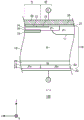
Fig. 1 is a diagram showing an example of the upper surface of a semiconductor device 100 according to the present embodiment. Fig. 1 shows a position where each component is projected onto the front surface of the semiconductor substrate 10. In fig. 1, only parts of a part of the semiconductor device 100 are shown, and parts of the other part are omitted.
The semiconductor device 100 includes a semiconductor substrate 10. The semiconductor substrate 10 has an end edge 102 in a plan view. In the present specification, the term "planar" refers to a front side of the semiconductor substrate 10. The semiconductor substrate 10 of this example has two sets of end edges 102 that face each other in a plan view. In fig. 1, the X-axis and Y-axis are parallel to either end edge 102. In addition, the Z axis is perpendicular to the front surface of the semiconductor substrate 10.
The semiconductor substrate 10 is provided with an active portion 160. The active portion 160 is a region in which main current flows between the front surface and the rear surface of the semiconductor substrate 10 in the depth direction when the semiconductor device 100 is operated. The emitter electrode is disposed above the active portion 160, but is omitted in fig. 1.
At least one of a transistor portion 70 including a transistor element such as an IGBT and a diode portion 80 including a diode element such as a flywheel diode (FWD) is provided in the active portion 160. In the example of fig. 1, the transistor portions 70 and the diode portions 80 are alternately arranged along a predetermined arrangement direction (in this example, the X-axis direction) of the front surface of the semiconductor substrate 10. In another example, only the transistor portion 70 may be provided in the active portion 160.
In fig. 1, the region where the transistor portion 70 is arranged is denoted by the reference numeral "I", and the region where the diode portion 80 is arranged is denoted by the reference numeral "F". In the present specification, a direction perpendicular to the arrangement direction in a plan view may be referred to as an extending direction (Y-axis direction in fig. 1). The transistor portion 70 and the diode portion 80 may have long sides in the extending direction, respectively. That is, the length of the transistor portion 70 in the Y-axis direction is larger than the width of the transistor portion 70 in the X-axis direction. Similarly, the length of the diode portion 80 in the Y-axis direction is larger than the width in the X-axis direction. The extending direction of the transistor portion 70 and the diode portion 80 may be the same as the longitudinal direction of each trench portion described later.
The transistor portion 70 has a p+ -type collector region in a region contacting the back surface of the semiconductor substrate 10. The diode portion 80 has an n+ -type cathode region in a region contacting the back surface of the semiconductor substrate 10. In this specification, a region where a collector region is provided is referred to as a transistor portion 70. That is, the transistor portion 70 is a region overlapping the collector region in a plan view.
An n+ -type cathode region may be provided on the back surface of the semiconductor substrate 10 in a region other than the collector region. In this specification, a cathode region is provided on a lower surface of an extension region extending the transistor portion 70 in the Y-axis direction to a gate runner described later. In this specification, the extension region is included in the diode portion 80. The transistor portion 70 is periodically provided with an N-type emitter region, a P-type base region, and a gate structure including a gate conductive portion and a gate insulating film on the front surface side of the semiconductor substrate 10.
The semiconductor device 100 may have one or more pads over the semiconductor substrate 10. As an example, the semiconductor device 100 shown in fig. 1 has the gate pad G, but this is merely an example. The semiconductor device 100 may have pads such as an anode pad, a cathode pad, and a current detection pad. Each pad is disposed near the end edge 102. The vicinity of the end edge 102 refers to an area between the end edge 102 and the emitter electrode in a plan view. When the semiconductor device 100 is actually mounted, each pad may be connected to an external circuit via a wiring such as a lead.
A gate potential is applied to the gate pad G. The gate pad G is electrically connected to the conductive portion of the gate trench portion of the active portion 160. The semiconductor device 100 includes a gate runner 48 electrically connecting the gate pad G and the gate trench portion.
The gate runner 48 is arranged between the active portion 160 and the end edge 102 of the semiconductor substrate 10 in plan view. The gate runner 48 of this example surrounds the active portion 160 in a plan view. The region surrounded by the gate runner 48 in a plan view may be the active portion 160.
The gate runner 48 is disposed above the semiconductor substrate 10. The gate runner 48 of this example may be formed of polysilicon doped with impurities or the like. The gate runner 48 is electrically connected to a gate conductive portion provided inside the gate trench portion via a gate insulating film.
The semiconductor device 100 of this example includes a voltage-resistant structure 190 provided on the outer periphery of the active portion 160. The pressure-resistant structure 190 of the present embodiment is disposed between the gate runner 48 and the end edge 102. The withstand voltage structure 190 relieves electric field concentration on the front side of the semiconductor substrate 10.
The pressure-resistant structure portion 190 may have a guard ring 92. Guard ring 92 is a P-type region that contacts the front surface of semiconductor substrate 10. The pressure-resistant structure 190 of the present embodiment includes a plurality of guard rings 92, but only one guard ring 92 is omitted from fig. 1. By providing the plurality of guard rings 92, the depletion layer on the upper surface side of the active portion 160 can be extended outward, and the withstand voltage of the semiconductor device 100 can be improved. The pressure-resistant structure 190 may further include at least one of a field plate provided in a ring shape surrounding the active portion 160 and reducing a surface electric field.
The semiconductor device 100 may include a temperature sensing portion, not shown, which is a PN junction diode formed of polysilicon or the like, and/or a current detecting portion, not shown, which operates in the same manner as a transistor portion provided in the active portion 160.
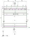
Fig. 2A is an enlarged view showing an example of the upper surface of the semiconductor device 100. Fig. 2A shows a region a shown in fig. 1, that is, a vicinity of a boundary between the active portion 160 and the pressure-resistant structure portion 190. The semiconductor device 100 includes a semiconductor substrate having a transistor portion 70 including a transistor element such as an IGBT and a diode portion 80 including a diode element such as a flywheel diode (FWD).
The transistor portions 70 and the diode portions 80 of this example are alternately arranged along the arrangement direction (in this example, the X-axis direction). The diode portion 80 is provided between the transistor portion 70 adjacent to the voltage-resistant structure portion 190 and the voltage-resistant structure portion 190 in a plan view. That is, the diode portion 80 is disposed at the outermost side of the active portion 160. In the present specification, the directions toward the center of the semiconductor device 100 are the inner side and the outer side, respectively, and the directions away from the center of the semiconductor device 100 are the outer side, respectively.
The semiconductor device 100 of this example includes a gate trench 40, a dummy trench 30, a well region 11, an emitter region 12, a base region 14, and a contact region 15, which are provided on the front side of a semiconductor substrate. The gate trench 40 and the dummy trench 30 are examples of the trench.
The semiconductor device 100 of this example includes a gate metal layer 50 and a emitter electrode 52 provided above the front surface of the semiconductor substrate. The gate metal layer 50 and the emitter electrode 52 are disposed separately from each other. The gate metal layer 50 is electrically insulated from the emitter electrode 52.
An interlayer insulating film is provided between the emitter electrode 52 and the front surface of the semiconductor substrate and between the gate metal layer 50 and the front surface of the semiconductor substrate, but is omitted in fig. 2A. In the interlayer insulating film of this example, a contact hole 49, a contact hole 54, and a contact hole 56 are provided so as to penetrate the interlayer insulating film. In fig. 2A, the respective contacts Kong Biaozhu are shaded diagonally.
The emitter electrode 52 is disposed over the gate trench portion 40, the dummy trench portion 30, the well region 11, the emitter region 12, the base region 14, and the contact region 15. The emitter electrode 52 is electrically connected to the emitter region 12, the base region 14 and the contact region 15 of the front side of the semiconductor substrate via the contact hole 54.
In addition, the emitter electrode 52 is connected to the dummy conductive portion in the dummy trench portion 30 through the contact hole 56. A connection portion 25 formed of a material having conductivity such as polysilicon doped with impurities may be provided between the emitter electrode 52 and the dummy conductive portion. The connection portion 25 is provided on the front surface of the semiconductor substrate with an insulating film such as an interlayer insulating film and a dummy insulating film of the dummy trench portion 30 interposed therebetween.
The gate metal layer 50 is electrically connected to the gate runner 48 through the contact hole 49. The gate runner 48 may be formed of polysilicon doped with impurities or the like. The gate runner 48 is connected to the gate conductive portion in the gate trench portion 40 at the front surface of the semiconductor substrate. The gate runner 48 is not electrically connected to the dummy conductive portion and the emitter electrode 52 within the dummy trench portion 30.
The gate runner 48 and the emitter electrode 52 are electrically separated by an insulating material such as an interlayer insulating film or an oxide film. The gate runner 48 of this example is provided from below the contact hole 49 to the front end portion of the gate trench portion 40. At the front end of the gate trench 40, a gate conductive portion is exposed on the front surface of the semiconductor substrate and connected to the gate runner 48.
The emitter electrode 52 and the gate metal layer 50 are formed of a conductive material containing a metal. For example, it is formed of aluminum or an alloy containing aluminum as a main component (for example, an aluminum-silicon alloy or the like). Each electrode may have a barrier metal formed of titanium, a titanium compound, or the like, on the lower layer of the region formed of aluminum or the like.
Each electrode may have a plug made of tungsten or the like in the contact hole. The plug may have a barrier metal on a side contacting the semiconductor substrate, and tungsten may be buried so as to contact the barrier metal, and aluminum may be formed on the tungsten.
The plug is provided in the contact hole that is in contact with the contact region 15 or the base region 14. In addition, a p++ type plug region having a higher doping concentration than the contact region 15 is formed under the contact hole of the plug. This can improve the contact resistance between the barrier metal and the contact region 15. The plug region has a depth of approximately 0.1 μm or less and has a region smaller than the contact region 15 by 10% or less.
The plug region has the following features. In the operation of the transistor portion 70, the latch-up resistance is improved by improving the contact resistance. On the other hand, in the diode portion 80 operation, when there is no plug region, the contact resistance between the barrier metal and the base region 14 is high, and the conduction loss and the switching loss increase.
The well region 11 overlaps the gate runner 48, extends around the outer periphery of the active portion 160, and is formed in a ring shape in plan view. The well region 11 extends by a predetermined width in a range not overlapping the gate runner 48, and is provided in a ring shape in a plan view. The well region 11 of this example is provided so as to be separated from the end of the contact hole 54 in the Y-axis direction toward the gate runner 48. The well region 11 is a region of the second conductivity type having a higher doping concentration than the base region 14. The gate runner 48 is electrically insulated from the well region 11.
The base region 14 in this example is P-type, and the well region 11 is p+ -type. Further, the well region 11 is formed from the front surface of the semiconductor substrate to a position deeper than the lower end of the base region 14. The base region 14 is provided in the transistor portion 70 and the diode portion 80 so as to be in contact with the well region 11. Thus, the well region 11 is electrically connected to the emitter electrode 52.
The transistor portion 70 and the diode portion 80 each have trench portions arranged in a plurality of rows in the arrangement direction. In the transistor portion 70 of this example, one or more gate trench portions 40 are provided along the arrangement direction. The diode portion 80 of this example is provided with a plurality of dummy trench portions 30 along the arrangement direction. The gate trench portion 40 is not provided in the diode portion 80 of this example.
The gate trench portion 40 of this example may have two straight portions 39 (portions of the trench that are straight along the extending direction) extending along the extending direction perpendicular to the arrangement direction, and a front end portion 41 connecting the two straight portions 39.
At least a part of the distal end portion 41 may be provided in a curved shape in a plan view. The ends of the two straight portions 39 in the Y-axis direction are connected to the gate runner 48 by the tip portions 41, and function as gate electrodes to the gate trench portions 40. On the other hand, by forming the front end portion 41 in a curve, the electric field concentration at the end portion can be relieved more than at the end of the straight portion 39.
In another example, the transistor portion 70 may be alternately provided with one or more gate trench portions 40 and one or more dummy trench portions 30 along the arrangement direction. In the transistor portion 70, the dummy trench portion 30 is disposed between the respective straight line portions 39 of the gate trench portion 40. One dummy trench portion 30 may be provided between the respective straight portions 39, or a plurality of dummy trench portions 30 may be provided.
In addition, the dummy trench portion 30 may not be provided between the respective straight portions 39, and the gate trench portion 40 may be provided. With such a structure, the electron current from the emitter region 12 can be increased, and thus the on-voltage decreases.
The dummy trench portion 30 may have a linear shape extending in the extending direction, or may have a linear portion 29 and a tip portion 31, similarly to the gate trench portion 40. Although the semiconductor device 100 shown in fig. 2A has only the dummy trench portions 30 having the front end portions 31 arranged, in another example, the semiconductor device 100 may include the dummy trench portions 30 having a straight shape without the front end portions 31.
The diffusion depth of the well region 11 may be deeper than the depths of the gate trench portion 40 and the dummy trench portion 30. The gate trench 40 and the dummy trench 30 are provided at the well region 11 in a top view at the ends in the Y-axis direction. That is, at the end of each trench in the Y-axis direction, the bottom of each trench in the depth direction is covered with the well region 11. The trench portion provided at the end in the X-axis direction may be covered with the well region 11. This can alleviate the electric field concentration at the bottom of each trench.
In the arrangement direction, a land portion is provided between the groove portions. The mesa portion is a region sandwiched by the trench portions in the semiconductor substrate. As an example, the depth position of the mesa portion is a position from the front surface of the semiconductor substrate to the lower end of the trench portion.
The mesa portion of this example is sandwiched by trench portions adjacent to each other in the X-axis direction, and is provided on the front surface of the semiconductor substrate so as to extend along the trench in the extending direction (Y-axis direction). As will be described later, in fig. 2B, in this example, the transistor portion 70 is provided with a mesa portion 60, and the diode portion 80 is provided with a mesa portion 61. In the present specification, the table portion 60 and the table portion 61 are referred to as "table portions" respectively.
A base region 14 is provided at each mesa portion. At least one of the emitter region 12 of the first conductivity type and the contact region 15 of the second conductivity type may be provided in a region sandwiched by the base regions 14 in a plan view on each mesa portion. The emitter region 12 in this example is of the n+ type and the contact region 15 is of the p+ type. The emitter region 12 and the contact region 15 may be disposed between the base region 14 and the front surface of the semiconductor substrate in the depth direction.
The mesa portion of the transistor portion 70 has the emitter region 12 exposed at the front surface of the semiconductor substrate. The emitter 12 is disposed adjacent to the gate trench 40. A contact region 15 exposed on the front surface of the semiconductor substrate is provided in the mesa portion which is in contact with the gate trench 40.
The contact region 15 and the emitter region 12 in the mesa portion are provided from one trench portion to the other trench portion, respectively, in the X-axis direction. As an example, the contact regions 15 and the emitter regions 12 of the mesa portion are alternately arranged along the extending direction (Y-axis direction) of the trench portion.
In another example, the contact region 15 and the emitter region 12 of the mesa portion may be arranged in a stripe shape along the extending direction (Y-axis direction) of the trench portion. For example, the emitter region 12 is provided in a region adjoining the trench portion, and the contact region 15 is provided in a region sandwiched by the emitter regions 12.
The emitter region 12 is not provided on the mesa portion of the diode portion 80. The base region 14 may be provided on the upper surface of the mesa portion of the diode portion 80. The base region 14 may be disposed over the entire mesa portion of the diode portion 80.
Contact holes 54 are provided above the respective mesa portions. The contact hole 54 is arranged in a region sandwiched by the base regions 14 in the extending direction (Y-axis direction) thereof. The contact hole 54 of this example is provided above the contact region 15, the base region 14 and the respective regions of the emitter region 12. The contact hole 54 may be arranged at the center in the arrangement direction (X-axis direction) of the mesa portions.
In the diode portion 80, an n+ -type cathode region 82 is provided in a region adjacent to the back surface of the semiconductor substrate. The p+ -type collector region 22 may be provided on the back surface of the semiconductor substrate in a region where the cathode region 82 is not provided. In fig. 2A, the boundary between the cathode region 82 and the collector region 22 is indicated by a broken line. In the pressure-resistant structure 190, the n+ type cathode region 82 may be provided on the back surface side of the semiconductor substrate.
Fig. 2B is a view showing a section a-a' in fig. 2A. The a-a' cross section is the XZ plane through the contact region 15, the base region 14, and the gate trench portion 40 and the dummy trench portion 30. The semiconductor device 100 of this example has the semiconductor substrate 10, the interlayer insulating film 38, the emitter electrode 52, and the collector electrode 24 in the section a-a'.
An interlayer insulating film 38 is provided on the front surface 21 of the semiconductor substrate 10. The interlayer insulating film 38 is an insulating film such as silicate glass to which impurities such as boron and phosphorus are added. The interlayer insulating film 38 may be in contact with the front surface 21, or another film such as an oxide film may be provided between the interlayer insulating film 38 and the front surface 21. The interlayer insulating film 38 is provided with a contact hole 54 described with reference to fig. 2A.
The emitter electrode 52 is provided on the front surface 21 of the semiconductor substrate 10 and the upper surface of the interlayer insulating film 38. The emitter electrode 52 is electrically connected to the front surface 21 through the contact hole 54 of the interlayer insulating film 38. A plug region 17 of tungsten (W) or the like may be provided inside the contact hole 54. The collector electrode 24 is provided on the back surface 23 of the semiconductor substrate 10. The emitter electrode 52 and the collector electrode 24 are formed of a material containing a metal or a laminated film thereof.
The semiconductor substrate 10 may be a silicon substrate, a silicon carbide substrate, a nitride semiconductor substrate such as gallium nitride, or the like. The semiconductor substrate 10 of this example is a silicon substrate.
The semiconductor substrate 10 has a drift region 18 of a first conductivity type. The drift region 18 in this example is of N-type. The drift region 18 may be a region remaining in the semiconductor substrate 10 without providing any other doped region.
In the transistor portion 70, one or more accumulation regions 16 may be provided above the drift region 18 in the Z-axis direction. The accumulation region 16 is a region in which the same dopant as the drift region 18 is accumulated so as to have a higher concentration than the drift region 18. The doping concentration of accumulation region 16 is higher than the doping concentration of drift region 18.
The accumulation region 16 in this example is N-type. Accumulation region 16 may be disposed between base region 14 and trench bottom 75 described later in transistor portion 70. The accumulation region 16 may be provided only in the transistor portion 70, or may be provided in both the transistor portion 70 and the diode portion 80. By providing the accumulation region 16, the carrier injection promoting effect (IE effect) can be improved, and the on-voltage can be reduced.
In the transistor portion 70, an emitter region 12 is provided above the base region 14 so as to contact the front surface 21. The emitter region 12 is grounded to the gate trench portion 40. The doping concentration of the emitter region 12 is higher than the doping concentration of the drift region 18. As an example, the dopants of the emitter region 12 are arsenic (As), phosphorus (P), antimony (Sb), and the like.
The diode portion 80 is provided with the base region 14 exposed at the front surface 21. The base region 14 of the diode unit 80 operates as an anode.
A buffer region 20 of the first conductivity type may be provided below the drift region 18. The buffer 20 of this example is N-type. The doping concentration of the buffer region 20 is higher than the doping concentration of the drift region 18. The buffer region 20 can function as a field stop layer that prevents the depletion layer that expands from the lower surface side of the base region 14 from reaching the collector region 22 and the cathode region 82.
In the transistor portion 70, a collector region 22 is provided below the buffer region 20. The collector region 22 may be disposed at the back surface 23 in contact with the cathode region 82.
In the diode portion 80, a cathode region 82 is provided below the buffer region 20. The cathode region 82 may be disposed at the same depth as the collector region 22 of the transistor portion 70. The diode unit 80 may function as a freewheeling diode (FWD) through which a reverse-on reflow current flows when the transistor unit 70 is turned off.
A gate trench portion 40 and a dummy trench portion 30 are provided in the semiconductor substrate 10. The gate trench 40 and the dummy trench 30 are provided so as to penetrate the base region 14 and the accumulation region 16 from the front surface 21 to reach the drift region 18. The trench portion penetrating the doped region is not limited to being manufactured in the order in which the trench portion is formed after the doped region is formed. After forming the trench portions, the case of forming the doped regions between the trench portions is also included in the case of penetrating the trench portions through the doped regions.
The gate trench portion 40 has a gate trench provided in the front surface 21, a gate insulating film 42, and a gate conductive portion 44. The gate insulating film 42 is provided so as to cover the inner wall of the gate trench. The gate insulating film 42 may be formed of an oxide film or a nitride film. The gate conductive portion 44 is provided so as to fill a portion inside the gate trench with the gate insulating film 42. The upper surface of the gate conductive portion 44 may be located in the same XY plane as the front surface 21. The gate insulating film 42 insulates the gate conductive portion 44 from the semiconductor substrate 10. The gate conductive portion 44 is formed of polysilicon doped with impurities or the like.
The gate conductive portion 44 may be provided longer than the base region 14 in the depth direction. The gate trench 40 is covered with an interlayer insulating film 38 on the front surface 21. If a predetermined voltage is applied to the gate conductive portion 44, a channel formed by an inversion layer of electrons is formed in the surface layer of the interface with the gate trench in the base region 14.
The dummy trench portion 30 may have the same structure as the gate trench portion 40 in XZ cross section. The dummy trench portion 30 has a dummy trench provided in the front surface 21, a dummy insulating film 32, and a dummy conductive portion 34. The dummy insulating film 32 is provided so as to cover the inner wall of the dummy trench. The dummy insulating film 32 may be formed of an oxide film or a nitride film. The dummy conductive portion 34 is provided so as to fill a portion inside the dummy trench with the dummy insulating film 32. The upper surface of the dummy conductive portion 34 may be located in the same XY plane as the front surface 21. The dummy insulating film 32 insulates the dummy conductive portions 34 from the semiconductor substrate 10. The dummy conductive portion 34 may be formed of the same material as the gate conductive portion 44.
The gate trench 40 and the dummy trench 30 of this example are covered with an interlayer insulating film 38 on the front surface 21. The bottoms of the dummy trench portions 30 and the gate trench portions 40 may be curved surfaces (curved in cross section) protruding downward.
The transistor portion 70 has a P-type trench bottom 75 provided at a lower end of the trench portion. The trench bottom 75 of this example is disposed below the accumulation region 16. The lower end of the trench bottom 75 may be located below the bottom of the gate trench 40 in the depth direction of the semiconductor substrate 10. In other words, the trench bottom 75 may cover the bottom of the gate trench portion 40.
The doping concentration of the trench bottom 75 is higher than the doping concentration of the drift region 18 and lower than the doping concentration of the base region 14. The doping concentration of the trench bottom 75 is 1E12cm -3 Above and 1E13cm -3 The following is given.
In fig. 2B, the end of the trench bottom 75 on the positive side (diode portion 80 side) in the X-axis direction coincides with the boundary between the cathode region 82 and the collector region 22, but may extend further toward the diode portion 80 side than the boundary between the cathode region 82 and the collector region 22, or may recede into the transistor portion 70.
The trench bottom 75 may be an electrically floating layer. In this specification, the floating layer refers to a layer that is not electrically connected to any electrode such as the emitter electrode 52. By providing the trench bottom portion 75, the on-state characteristics of the transistor portion 70 are improved. In addition, by providing the trench bottom 75, electric field concentration at the bottom of the gate trench 40 is relieved, and avalanche resistance is improved.
Fig. 2C is a view showing a section b-b' in fig. 2A. The section b-b' is the YZ plane passing through the base region 14 and the contact region 15 provided in the diode portion 80 near the Y-axis negative side end portion of the active portion 160.
In this example, the diode portion 80 is provided at the outermost side of the active portion 160. In the diode portion 80, the contact region 15 is provided on the front surface 21 of the semiconductor substrate 10. In the diode portion 80, the base region 14 is exposed on the front surface 21 of the semiconductor substrate 10 on the outer side of the contact region 15 in the Y-axis direction. That is, in the diode portion 80, the contact region 15 is sandwiched by the base regions 14 in the Y-axis direction in a plan view.
A well region 11 is provided near the Y-axis negative side end of the active portion 160. The well region 11 has a deeper diffusion depth than the base region 14. The well region 11 may extend in the Y-axis direction in such a manner as to partially cover the bottom of the base region 14.
Fig. 2D is a view showing a section c-c' in fig. 2A. The c-c' section is a YZ plane passing through the emitter 12, the base 14, and the contact 15 of the transistor portion 70 near the negative Y-axis end of the active portion 160. The c-c' section is an extension region formed by extending the transistor portion 70 in the Y-axis direction. A cathode region is disposed on the lower surface of the extension region. That is, the transistor portion 70 is sandwiched by the diode portion 80 in the Y-axis direction in a plan view.
In the transistor portion 70, an emitter region 12 and a contact region 15 are provided on the front surface 21 of the semiconductor substrate 10. In the transistor portion 70, the base region 14 is exposed on the front surface 21 of the semiconductor substrate 10 on the outer side of the contact region 15 in the Y-axis direction. That is, in the transistor portion 70, the emitter region 12 and the contact region 15 are sandwiched by the base region 14 in the Y-axis direction in a plan view.
In the transistor portion 70, the accumulation region 16 and the trench bottom 75 are provided above the drift region 18. The trench bottom 75 is disposed below the accumulation region 16. The trench bottom 75 may be disposed in contact with the lower surface of the accumulation region 16. Alternatively, as will be described later, the trench bottom 75 may be separated from the accumulation region 16, that is, the drift region 18 may be interposed between the accumulation region 16 and the trench bottom 75.
Fig. 2E is a view showing another example of the section a-a' in fig. 2A. The section a-a' is the XZ plane passing through the contact region 15, the base region 14, and the gate trench 40 and the dummy trench 30, as in fig. 2B. The semiconductor device 100 of this example has a semiconductor substrate 10, an interlayer insulating film 38, a emitter electrode 52, and a collector electrode 24 in the section a-a'.
The difference from fig. 2B is that the trench bottom 75 of the transistor portion 70 provided at the lower end of the trench portion is thinner than the accumulation region 16 in the depth direction of the semiconductor substrate 10 from the trench bottom 75 of fig. 2B.
The lower end of the trench bottom 75 of this example is located below the bottom of the gate trench 40 and covers the bottom of the gate trench 40.
The trench bottom 75 may be an electrically floating layer.
In fig. 2E, the end of the trench bottom 75 on the positive side (diode portion 80 side) in the X-axis direction coincides with the boundary between the cathode region 82 and the collector region 22, but may extend further toward the diode portion 80 side than the boundary between the cathode region 82 and the collector region 22, or may recede into the transistor portion 70. The same effects as those of fig. 2B can be obtained in this example.
Fig. 2F is a view showing another example of the section a-a' in fig. 2A. The a-a' section is the XZ plane passing through the contact region 15, the base region 14, and the gate trench 40 and the dummy trench 30 as in fig. 2B. The semiconductor device 100 of this example has a semiconductor substrate 10, an interlayer insulating film 38, a emitter electrode 52, and a collector electrode 24 in the section a-a'.
The difference between the trench bottom 75 and the accumulation region 16 in fig. 2G and the trench bottom 75 is that the drift region 18 is interposed between the accumulation region 16 and the trench bottom 75, as shown in fig. 2B and 2F.
The thickness of the trench bottom 75 may be thinner than the thickness of the accumulation region 16 or the thickness of the drift region 18 between the accumulation region 16 and the trench bottom 75 in the depth direction of the semiconductor substrate 10.
In fig. 2F, the end of the trench bottom 75 on the positive side (diode portion 80 side) in the X-axis direction coincides with the boundary between the cathode region 82 and the collector region 22, but may extend further toward the diode portion 80 side than the boundary between the cathode region 82 and the collector region 22, or may recede into the transistor portion 70. The same effects as those of fig. 2B can be obtained in this example.
Fig. 3A is a diagram showing an example of arrangement of the trench bottom region Rp and the electron passing region Rn. Fig. 3B is a view showing a section d-d' in fig. 3A. The trench bottom 75 of this example is intermittently provided in the transistor portion 70. The transistor portion 70 has electron passing portions 77 provided between the trench bottom portions 75 at the same positions in the Z-axis direction as the trench bottom portions 75. In fig. 3B, although the range of the electron passing portion 77 is shown by hatching, the electron passing portion 77 is the same N-type region as the drift region 18, and may be a part of the drift region 18.
In the present specification, a region corresponding to the trench bottom 75 in plan view is referred to as a trench bottom region Rp, and a region corresponding to the electron passing portion 77 in plan view is referred to as an electron passing region Rn. The transistor portion 70 of this example has an electron transit region Rn in a plan view where the trench bottom 75 is not provided.
The electron passing region Rn is provided to extend from the groove portion to the adjacent groove portion in the X-axis direction. That is, as shown in fig. 3A, the electron transit region Rn is provided so as to extend over the mesa portion in the X-axis direction. In fig. 3A, only the gate trench 40 is shown as a trench, but the present invention is not limited thereto. The electron passing region Rn is provided so as to extend in the X-axis direction across the mesa portion between adjacent two of the plurality of dummy trench portions 30 and the gate trench portion 40.
The electron transit regions Rn may extend across the plurality of groove portions in the X-axis direction. That is, the electron transit regions Rn may extend parallel to the emission regions 12 in a plan view.
In this example, the emission region 12 is not provided on the mesa portion of the electron transit region Rn. That is, as shown in fig. 3B, the emitter region 12 is not provided above the electron passing portion 77, and the trench bottom 75 is provided below the emitter region 12. As shown in fig. 3A, the electron passing region Rn is provided so that the Y-axis direction end portion is located in the contact region 15 in a plan view.
If the trench bottom region Rp is provided over the entire transistor portion 70, the transient resistance increases until the potential of the trench bottom 75 increases when the transistor portion 70 is turned on, and thus the on-resistance may be deteriorated.
In this example, when the transistor portion 70 is turned on, electrons from the emitter region 12 first pass through the electron passing portion 7 to the collector region 22. After that, if holes from the collector region 22 accumulate in the trench bottom 75, electrons pass through the trench bottom 75, and reach conduction. In this way, since the transistor portion 70 has the electron transit region Rn, an increase in transient resistance when the transistor portion 70 is turned on is suppressed, and on-resistance is improved.
In the electron passing portion 77, avalanche is likely to occur due to current concentration. However, in this example, by not providing the emission region 12 on the mesa portion of the electron passing region Rn, the possibility of occurrence of latch-up in the electron passing portion 77 can be reduced. In this way, in this example, by providing the trench bottom 75 below the emitter region 12, it is possible to improve the on-characteristic and improve the on-resistance.
Fig. 4A is a diagram showing an example of arrangement of the trench bottom region Rp and the electron passing region Rn. Fig. 4B is a view showing a section e-e' in fig. 4A. As in fig. 3A and 3B, the trench bottom portions 75 of the present example are provided intermittently in the transistor portion 70, and the transistor portion 70 has electron passing portions 77 provided between the trench bottom portions 75 at the same Z-axis direction positions as the trench bottom portions 75.
As in fig. 3A and 3B, the electron transit regions Rn of this example are provided to extend from the groove portion to the adjacent groove portion in the X-axis direction. That is, the electron transit region Rn is provided so as to extend over the mesa portion in the X-axis direction. In addition, the electron transit regions Rn may extend across the plurality of groove portions in the X-axis direction. That is, the electron passing region Rn may extend perpendicularly to the trench portion in a plan view.
Unlike fig. 3A and 3B, at least the emission region 12 is provided in the electron passing region Rn of this example. That is, an electron passing portion 77 is provided below any one of the emission regions 12. Thus, when the transistor portion 70 is turned on, electrons from the emitter region 12 can reliably pass through the electron passing portion 77. In this way, since the transistor portion 70 has the electron transit region Rn, an increase in transient resistance when the transistor portion 70 is turned on is suppressed, and on-resistance is improved.
Fig. 5A is a diagram showing an example of arrangement of the trench bottom region Rp and the electron passing region Rn. Fig. 5B is a view showing a section f-f' in fig. 5A. As in fig. 3A to 4B, the trench bottom portions 75 of the present example are provided intermittently in the transistor portion 70, and the transistor portion 70 has electron passing portions 77 provided between the trench bottom portions 75 at the same positions in the Z-axis direction as the trench bottom portions 75.
Unlike fig. 3A to 4B, in this example, the trench bottom regions Rp and the electron passing regions Rn are alternately arranged in the X-axis direction. That is, as shown in fig. 5A, the trench bottom regions Rp and the electron passing regions Rn are alternately arranged extending parallel to the gate trench portion 40 in a plan view.
At least the gate trench portion 40 may be provided in the electron passing region Rn. That is, an electron passing portion 77 is provided below any of the gate trench portions 40. If a channel is formed in the gate trench portion 40 provided in the electron transit region Rn, electrons from the channel can reliably pass through the electron transit portion 77 below. In this way, since the transistor portion 70 has the electron transit region Rn, an increase in transient resistance when the transistor portion 70 is turned on is suppressed, and on-resistance is improved.
Although the present invention has been described with reference to the embodiments, the technical scope of the present invention is not limited to the scope described in the above embodiments. Various alterations and modifications to the above-described embodiments will be apparent to those skilled in the art. It is apparent from the description of the claims that the embodiments to which such changes and modifications are applied can be included in the technical scope of the present invention.
Note that the order of execution of the respective processes such as the operations, procedures, steps, and stages in the apparatus, system, program, and method shown in the claims, the specification, and the drawings may be in any order unless the result of the previous process is used in the subsequent process, unless specifically indicated as "earlier", or the like. The operation flows in the claims, specification, and drawings do not necessarily have to be performed in this order, even though "first", "next", and the like are described for convenience.
Claims (13)
1. A semiconductor device includes a transistor portion,
the semiconductor device includes:
a drift region of a first conductivity type provided on the semiconductor substrate;
a plurality of trench portions extending from the front surface of the semiconductor substrate to the drift region;
an emission region of a first conductivity type provided to extend from a trench portion to an adjacent trench portion among the plurality of trench portions at a front surface of the semiconductor substrate, and having a doping concentration higher than that of the drift region; and
a second conductivity type trench bottom portion provided at a lower end of the trench portion,
The transistor portion has an electron passing region in a plan view, in which the trench bottom is not provided.
2. The semiconductor device according to claim 1, wherein,
the electron passing region is provided to extend from a trench portion to an adjacent trench portion of the plurality of trench portions in a trench arrangement direction.
3. The semiconductor device according to claim 2, wherein,
the electron passing region extends across the plurality of trench portions in the trench arrangement direction.
4. A semiconductor device according to any one of claim 1 to 3, wherein,
the emitter region is not provided at the mesa portion of the electron passing region.
5. The semiconductor device according to any one of claims 1 to 4, wherein,
the bottom of the groove is arranged below the emitting area.
6. The semiconductor device according to any one of claims 1 to 5, wherein,
the semiconductor device further includes a contact region of a second conductivity type provided on a front surface of the semiconductor substrate,
the electron passing region is provided so that an end in the direction of extending the trench is located in the contact region in a plan view.
7. A semiconductor device according to any one of claim 1 to 3, wherein,
At least the emission region is provided in the electron passing region.
8. A semiconductor device according to any one of claim 1 to 3, wherein,
the transistor portion has a trench bottom region formed with the trench bottom in a plan view,
the trench bottom regions and the electron passing regions are alternately arranged in the trench arrangement direction.
9. The semiconductor device according to claim 8, wherein at least a gate trench portion to which a gate voltage is applied is provided in the electron passing region.
10. The semiconductor device according to any one of claims 1 to 9, wherein,
the trench bottom is electrically floating.
11. The semiconductor device according to any one of claims 1 to 10, wherein a doping concentration of the trench bottom is 1E12cm -3 Above and 1E13cm -3 The following is given.
12. The semiconductor device according to any one of claims 1 to 11, further comprising an accumulation region of the first conductivity type provided above the drift region.
13. The semiconductor device according to claim 12, wherein,
the drift region is between the accumulation region and the trench bottom.
Applications Claiming Priority (3)
| Application Number | Priority Date | Filing Date | Title |
|---|---|---|---|
| JP2021080625 | 2021-05-11 | ||
| JP2021-080625 | 2021-05-11 | ||
| PCT/JP2021/045159 WO2022239285A1 (en) | 2021-05-11 | 2021-12-08 | Semiconductor device |
Publications (2)
| Publication Number | Publication Date |
|---|---|
| CN116349006A true CN116349006A (en) | 2023-06-27 |
| CN116349006A9 CN116349006A9 (en) | 2023-07-25 |
Family
ID=84028093
Family Applications (1)
| Application Number | Title | Priority Date | Filing Date |
|---|---|---|---|
| CN202180072875.0A Pending CN116349006A (en) | 2021-05-11 | 2021-12-08 | Semiconductor device with a semiconductor device having a plurality of semiconductor chips |
Country Status (5)
| Country | Link |
|---|---|
| US (1) | US20230261095A1 (en) |
| JP (1) | JPWO2022239285A1 (en) |
| CN (1) | CN116349006A (en) |
| DE (1) | DE112021004603T5 (en) |
| WO (1) | WO2022239285A1 (en) |
Cited By (1)
| Publication number | Priority date | Publication date | Assignee | Title |
|---|---|---|---|---|
| CN117577669A (en) * | 2023-11-16 | 2024-02-20 | 浙江旺荣半导体有限公司 | Reverse-conduction insulated gate bipolar transistor |
Families Citing this family (1)
| Publication number | Priority date | Publication date | Assignee | Title |
|---|---|---|---|---|
| JPWO2023140254A1 (en) * | 2022-01-20 | 2023-07-27 |
Family Cites Families (5)
| Publication number | Priority date | Publication date | Assignee | Title |
|---|---|---|---|---|
| JP5396953B2 (en) * | 2009-03-19 | 2014-01-22 | 株式会社デンソー | Silicon carbide semiconductor device and manufacturing method thereof |
| JP5013436B2 (en) * | 2009-06-04 | 2012-08-29 | 三菱電機株式会社 | Power semiconductor device |
| DE102013213026A1 (en) * | 2013-07-03 | 2015-01-08 | Robert Bosch Gmbh | Field plate trench FET and a semiconductor device |
| DE102017124871B4 (en) | 2017-10-24 | 2021-06-17 | Infineon Technologies Ag | Power semiconductor device and method for manufacturing a power semiconductor device |
| JP7404702B2 (en) * | 2019-08-09 | 2023-12-26 | 富士電機株式会社 | semiconductor equipment |
-
2021
- 2021-12-08 DE DE112021004603.9T patent/DE112021004603T5/en active Pending
- 2021-12-08 CN CN202180072875.0A patent/CN116349006A/en active Pending
- 2021-12-08 WO PCT/JP2021/045159 patent/WO2022239285A1/en unknown
- 2021-12-08 JP JP2023520757A patent/JPWO2022239285A1/ja active Pending
-
2023
- 2023-04-18 US US18/302,773 patent/US20230261095A1/en active Pending
Cited By (1)
| Publication number | Priority date | Publication date | Assignee | Title |
|---|---|---|---|---|
| CN117577669A (en) * | 2023-11-16 | 2024-02-20 | 浙江旺荣半导体有限公司 | Reverse-conduction insulated gate bipolar transistor |
Also Published As
| Publication number | Publication date |
|---|---|
| WO2022239285A1 (en) | 2022-11-17 |
| US20230261095A1 (en) | 2023-08-17 |
| JPWO2022239285A1 (en) | 2022-11-17 |
| CN116349006A9 (en) | 2023-07-25 |
| DE112021004603T5 (en) | 2023-06-15 |
Similar Documents
| Publication | Publication Date | Title |
|---|---|---|
| US20230261095A1 (en) | Semiconductor device | |
| US20230071170A1 (en) | Semiconductor device | |
| JP7211516B2 (en) | semiconductor equipment | |
| US20230268342A1 (en) | Semiconductor device | |
| CN111247639B (en) | Semiconductor device with a semiconductor device having a plurality of semiconductor chips | |
| CN111052394B (en) | Semiconductor device with a semiconductor device having a plurality of semiconductor chips | |
| JP7459976B2 (en) | semiconductor equipment | |
| JP7456113B2 (en) | Semiconductor Device | |
| JP7231064B2 (en) | semiconductor equipment | |
| JP7231065B2 (en) | semiconductor equipment | |
| WO2023224059A1 (en) | Semiconductor device | |
| US20240072110A1 (en) | Semiconductor device and manufacturing method of semiconductor device | |
| JP7468786B2 (en) | Semiconductor device and manufacturing method | |
| CN117099215A (en) | Semiconductor device with a semiconductor device having a plurality of semiconductor chips | |
| JP2024035557A (en) | semiconductor equipment | |
| CN116457944A (en) | Semiconductor device with a semiconductor device having a plurality of semiconductor chips | |
| CN117096184A (en) | Semiconductor device with a semiconductor device having a plurality of semiconductor chips | |
| JP2022161688A (en) | Semiconductor device | |
| CN117561612A (en) | Semiconductor device with a semiconductor device having a plurality of semiconductor chips | |
| CN115377098A (en) | Semiconductor device with a plurality of semiconductor chips | |
| CN116705842A (en) | Semiconductor device with a semiconductor device having a plurality of semiconductor chips | |
| CN117397038A (en) | Semiconductor device with a semiconductor device having a plurality of semiconductor chips | |
| CN112470288A (en) | Semiconductor device with a plurality of semiconductor chips | |
| CN112640129A (en) | Semiconductor device with a plurality of semiconductor chips |
Legal Events
| Date | Code | Title | Description |
|---|---|---|---|
| PB01 | Publication | ||
| PB01 | Publication | ||
| SE01 | Entry into force of request for substantive examination | ||
| SE01 | Entry into force of request for substantive examination | ||
| CI02 | Correction of invention patent application |
Correction item: A claim in accordance with Article nineteenth of the treaty Correct: Publication of text records and modification of claims in accordance with Article 19 of the Treaty False: The published text does not record the amended claims in accordance with Article 19 of the Treaty Number: 26-01 Page: ?? Volume: 39 |
|
| CI02 | Correction of invention patent application |