CN106873259B - Liquid crystal display device and semiconductor device - Google Patents
Liquid crystal display device and semiconductor device Download PDFInfo
- Publication number
- CN106873259B CN106873259B CN201610952614.9A CN201610952614A CN106873259B CN 106873259 B CN106873259 B CN 106873259B CN 201610952614 A CN201610952614 A CN 201610952614A CN 106873259 B CN106873259 B CN 106873259B
- Authority
- CN
- China
- Prior art keywords
- film
- electrode
- liquid crystal
- wiring
- insulating film
- Prior art date
- Legal status (The legal status is an assumption and is not a legal conclusion. Google has not performed a legal analysis and makes no representation as to the accuracy of the status listed.)
- Active
Links
- 239000004973 liquid crystal related substance Substances 0.000 title claims abstract description 328
- 239000004065 semiconductor Substances 0.000 title claims abstract description 196
- 239000000758 substrate Substances 0.000 claims abstract description 225
- 229910052581 Si3N4 Inorganic materials 0.000 claims description 27
- HQVNEWCFYHHQES-UHFFFAOYSA-N silicon nitride Chemical compound N12[Si]34N5[Si]62N3[Si]51N64 HQVNEWCFYHHQES-UHFFFAOYSA-N 0.000 claims description 27
- 230000000153 supplemental effect Effects 0.000 claims description 25
- 230000000295 complement effect Effects 0.000 claims description 24
- 229910052782 aluminium Inorganic materials 0.000 claims description 23
- XAGFODPZIPBFFR-UHFFFAOYSA-N aluminium Chemical compound [Al] XAGFODPZIPBFFR-UHFFFAOYSA-N 0.000 claims description 22
- 239000011521 glass Substances 0.000 claims description 22
- ZOKXTWBITQBERF-UHFFFAOYSA-N Molybdenum Chemical compound [Mo] ZOKXTWBITQBERF-UHFFFAOYSA-N 0.000 claims description 20
- 229910052750 molybdenum Inorganic materials 0.000 claims description 20
- 239000011733 molybdenum Substances 0.000 claims description 20
- OAICVXFJPJFONN-UHFFFAOYSA-N Phosphorus Chemical compound [P] OAICVXFJPJFONN-UHFFFAOYSA-N 0.000 claims description 17
- 229910052698 phosphorus Inorganic materials 0.000 claims description 17
- 239000011574 phosphorus Substances 0.000 claims description 17
- 229910021420 polycrystalline silicon Inorganic materials 0.000 claims description 14
- 229910021417 amorphous silicon Inorganic materials 0.000 claims description 12
- 229920005591 polysilicon Polymers 0.000 claims description 11
- 229910052785 arsenic Inorganic materials 0.000 claims description 9
- RQNWIZPPADIBDY-UHFFFAOYSA-N arsenic atom Chemical compound [As] RQNWIZPPADIBDY-UHFFFAOYSA-N 0.000 claims description 9
- 239000010408 film Substances 0.000 abstract description 717
- 230000005684 electric field Effects 0.000 abstract description 71
- 239000010409 thin film Substances 0.000 abstract description 62
- 239000012535 impurity Substances 0.000 description 131
- 239000010410 layer Substances 0.000 description 100
- 239000011229 interlayer Substances 0.000 description 79
- 239000000463 material Substances 0.000 description 70
- 238000000034 method Methods 0.000 description 62
- 230000000694 effects Effects 0.000 description 54
- 238000004519 manufacturing process Methods 0.000 description 51
- 230000002829 reductive effect Effects 0.000 description 49
- XUIMIQQOPSSXEZ-UHFFFAOYSA-N Silicon Chemical compound [Si] XUIMIQQOPSSXEZ-UHFFFAOYSA-N 0.000 description 45
- 229910052710 silicon Inorganic materials 0.000 description 45
- 239000010703 silicon Substances 0.000 description 45
- VYPSYNLAJGMNEJ-UHFFFAOYSA-N silicon dioxide Inorganic materials O=[Si]=O VYPSYNLAJGMNEJ-UHFFFAOYSA-N 0.000 description 43
- 229910052814 silicon oxide Inorganic materials 0.000 description 38
- IJGRMHOSHXDMSA-UHFFFAOYSA-N Atomic nitrogen Chemical compound N#N IJGRMHOSHXDMSA-UHFFFAOYSA-N 0.000 description 36
- 229910052751 metal Inorganic materials 0.000 description 30
- 239000002184 metal Substances 0.000 description 30
- 230000006870 function Effects 0.000 description 25
- 239000011159 matrix material Substances 0.000 description 25
- XLOMVQKBTHCTTD-UHFFFAOYSA-N Zinc monoxide Chemical compound [Zn]=O XLOMVQKBTHCTTD-UHFFFAOYSA-N 0.000 description 24
- PXHVJJICTQNCMI-UHFFFAOYSA-N Nickel Chemical compound [Ni] PXHVJJICTQNCMI-UHFFFAOYSA-N 0.000 description 22
- 229910010272 inorganic material Inorganic materials 0.000 description 22
- 239000011147 inorganic material Substances 0.000 description 22
- 239000011368 organic material Substances 0.000 description 19
- 229920002120 photoresistant polymer Polymers 0.000 description 19
- 238000005530 etching Methods 0.000 description 18
- 229910052757 nitrogen Inorganic materials 0.000 description 18
- QVGXLLKOCUKJST-UHFFFAOYSA-N atomic oxygen Chemical compound [O] QVGXLLKOCUKJST-UHFFFAOYSA-N 0.000 description 17
- AMGQUBHHOARCQH-UHFFFAOYSA-N indium;oxotin Chemical compound [In].[Sn]=O AMGQUBHHOARCQH-UHFFFAOYSA-N 0.000 description 17
- 229910052760 oxygen Inorganic materials 0.000 description 17
- 239000001301 oxygen Substances 0.000 description 17
- 239000010936 titanium Substances 0.000 description 17
- 150000001875 compounds Chemical class 0.000 description 16
- 239000000126 substance Substances 0.000 description 16
- 239000002356 single layer Substances 0.000 description 15
- 239000013078 crystal Substances 0.000 description 14
- RTAQQCXQSZGOHL-UHFFFAOYSA-N Titanium Chemical compound [Ti] RTAQQCXQSZGOHL-UHFFFAOYSA-N 0.000 description 13
- 238000005247 gettering Methods 0.000 description 13
- 238000010438 heat treatment Methods 0.000 description 13
- 230000008569 process Effects 0.000 description 13
- 239000010949 copper Substances 0.000 description 12
- BASFCYQUMIYNBI-UHFFFAOYSA-N platinum Chemical compound [Pt] BASFCYQUMIYNBI-UHFFFAOYSA-N 0.000 description 12
- 229910052719 titanium Inorganic materials 0.000 description 12
- 239000011651 chromium Substances 0.000 description 10
- 238000009792 diffusion process Methods 0.000 description 10
- 239000007789 gas Substances 0.000 description 10
- 239000010931 gold Substances 0.000 description 9
- 229910052759 nickel Inorganic materials 0.000 description 9
- 229920005989 resin Polymers 0.000 description 9
- 239000011347 resin Substances 0.000 description 9
- -1 resist Chemical class 0.000 description 9
- YVTHLONGBIQYBO-UHFFFAOYSA-N zinc indium(3+) oxygen(2-) Chemical compound [O--].[Zn++].[In+3] YVTHLONGBIQYBO-UHFFFAOYSA-N 0.000 description 9
- 239000011787 zinc oxide Substances 0.000 description 9
- GYHNNYVSQQEPJS-UHFFFAOYSA-N Gallium Chemical compound [Ga] GYHNNYVSQQEPJS-UHFFFAOYSA-N 0.000 description 8
- 229910052779 Neodymium Inorganic materials 0.000 description 8
- 239000004642 Polyimide Substances 0.000 description 8
- 230000004888 barrier function Effects 0.000 description 8
- 239000003990 capacitor Substances 0.000 description 8
- 239000003086 colorant Substances 0.000 description 8
- 229910052802 copper Inorganic materials 0.000 description 8
- 238000002425 crystallisation Methods 0.000 description 8
- 230000008025 crystallization Effects 0.000 description 8
- 229910052733 gallium Inorganic materials 0.000 description 8
- 229920001721 polyimide Polymers 0.000 description 8
- 239000005083 Zinc sulfide Substances 0.000 description 7
- 239000000919 ceramic Substances 0.000 description 7
- 239000000460 chlorine Substances 0.000 description 7
- 239000004020 conductor Substances 0.000 description 7
- 230000007547 defect Effects 0.000 description 7
- 230000010355 oscillation Effects 0.000 description 7
- 229920000642 polymer Polymers 0.000 description 7
- 229910052709 silver Inorganic materials 0.000 description 7
- 229910052984 zinc sulfide Inorganic materials 0.000 description 7
- ZOXJGFHDIHLPTG-UHFFFAOYSA-N Boron Chemical compound [B] ZOXJGFHDIHLPTG-UHFFFAOYSA-N 0.000 description 6
- RYGMFSIKBFXOCR-UHFFFAOYSA-N Copper Chemical compound [Cu] RYGMFSIKBFXOCR-UHFFFAOYSA-N 0.000 description 6
- BQCADISMDOOEFD-UHFFFAOYSA-N Silver Chemical compound [Ag] BQCADISMDOOEFD-UHFFFAOYSA-N 0.000 description 6
- UCKMPCXJQFINFW-UHFFFAOYSA-N Sulphide Chemical compound [S-2] UCKMPCXJQFINFW-UHFFFAOYSA-N 0.000 description 6
- 230000002159 abnormal effect Effects 0.000 description 6
- 230000005540 biological transmission Effects 0.000 description 6
- 229910052796 boron Inorganic materials 0.000 description 6
- 229910052804 chromium Inorganic materials 0.000 description 6
- 238000010586 diagram Methods 0.000 description 6
- 230000001678 irradiating effect Effects 0.000 description 6
- 239000011777 magnesium Substances 0.000 description 6
- 229920003023 plastic Polymers 0.000 description 6
- 239000004033 plastic Substances 0.000 description 6
- 230000006798 recombination Effects 0.000 description 6
- 238000005215 recombination Methods 0.000 description 6
- LIVNPJMFVYWSIS-UHFFFAOYSA-N silicon monoxide Chemical compound [Si-]#[O+] LIVNPJMFVYWSIS-UHFFFAOYSA-N 0.000 description 6
- 239000004332 silver Substances 0.000 description 6
- 229910052715 tantalum Inorganic materials 0.000 description 6
- 238000002834 transmittance Methods 0.000 description 6
- WFKWXMTUELFFGS-UHFFFAOYSA-N tungsten Chemical compound [W] WFKWXMTUELFFGS-UHFFFAOYSA-N 0.000 description 6
- 229910052721 tungsten Inorganic materials 0.000 description 6
- 239000010937 tungsten Substances 0.000 description 6
- 244000126211 Hericium coralloides Species 0.000 description 5
- 230000008901 benefit Effects 0.000 description 5
- 239000011230 binding agent Substances 0.000 description 5
- 230000008859 change Effects 0.000 description 5
- 229910052801 chlorine Inorganic materials 0.000 description 5
- PCHJSUWPFVWCPO-UHFFFAOYSA-N gold Chemical compound [Au] PCHJSUWPFVWCPO-UHFFFAOYSA-N 0.000 description 5
- 229910052737 gold Inorganic materials 0.000 description 5
- QEFYFXOXNSNQGX-UHFFFAOYSA-N neodymium atom Chemical compound [Nd] QEFYFXOXNSNQGX-UHFFFAOYSA-N 0.000 description 5
- 230000002093 peripheral effect Effects 0.000 description 5
- 230000000087 stabilizing effect Effects 0.000 description 5
- OKTJSMMVPCPJKN-UHFFFAOYSA-N Carbon Chemical compound [C] OKTJSMMVPCPJKN-UHFFFAOYSA-N 0.000 description 4
- VYZAMTAEIAYCRO-UHFFFAOYSA-N Chromium Chemical compound [Cr] VYZAMTAEIAYCRO-UHFFFAOYSA-N 0.000 description 4
- KRHYYFGTRYWZRS-UHFFFAOYSA-N Fluorane Chemical compound F KRHYYFGTRYWZRS-UHFFFAOYSA-N 0.000 description 4
- 239000004952 Polyamide Substances 0.000 description 4
- 229910009372 YVO4 Inorganic materials 0.000 description 4
- UBSJOWMHLJZVDJ-UHFFFAOYSA-N aluminum neodymium Chemical compound [Al].[Nd] UBSJOWMHLJZVDJ-UHFFFAOYSA-N 0.000 description 4
- 150000001408 amides Chemical class 0.000 description 4
- 239000012298 atmosphere Substances 0.000 description 4
- 239000003779 heat-resistant material Substances 0.000 description 4
- 239000012212 insulator Substances 0.000 description 4
- 239000012528 membrane Substances 0.000 description 4
- 239000010955 niobium Substances 0.000 description 4
- 150000004767 nitrides Chemical class 0.000 description 4
- 230000003287 optical effect Effects 0.000 description 4
- 229910052697 platinum Inorganic materials 0.000 description 4
- 229920002647 polyamide Polymers 0.000 description 4
- 239000010453 quartz Substances 0.000 description 4
- 230000009467 reduction Effects 0.000 description 4
- 239000003566 sealing material Substances 0.000 description 4
- 229910021332 silicide Inorganic materials 0.000 description 4
- GUVRBAGPIYLISA-UHFFFAOYSA-N tantalum atom Chemical compound [Ta] GUVRBAGPIYLISA-UHFFFAOYSA-N 0.000 description 4
- ZAMOUSCENKQFHK-UHFFFAOYSA-N Chlorine atom Chemical compound [Cl] ZAMOUSCENKQFHK-UHFFFAOYSA-N 0.000 description 3
- 229910052691 Erbium Inorganic materials 0.000 description 3
- MWUXSHHQAYIFBG-UHFFFAOYSA-N Nitric oxide Chemical compound O=[N] MWUXSHHQAYIFBG-UHFFFAOYSA-N 0.000 description 3
- 229910052775 Thulium Inorganic materials 0.000 description 3
- ATJFFYVFTNAWJD-UHFFFAOYSA-N Tin Chemical compound [Sn] ATJFFYVFTNAWJD-UHFFFAOYSA-N 0.000 description 3
- 229910052769 Ytterbium Inorganic materials 0.000 description 3
- NIXOWILDQLNWCW-UHFFFAOYSA-N acrylic acid group Chemical group C(C=C)(=O)O NIXOWILDQLNWCW-UHFFFAOYSA-N 0.000 description 3
- 230000009471 action Effects 0.000 description 3
- 230000002411 adverse Effects 0.000 description 3
- 239000000956 alloy Substances 0.000 description 3
- PNEYBMLMFCGWSK-UHFFFAOYSA-N aluminium oxide Inorganic materials [O-2].[O-2].[O-2].[Al+3].[Al+3] PNEYBMLMFCGWSK-UHFFFAOYSA-N 0.000 description 3
- 230000015572 biosynthetic process Effects 0.000 description 3
- 239000002041 carbon nanotube Substances 0.000 description 3
- 229910021393 carbon nanotube Inorganic materials 0.000 description 3
- 238000000576 coating method Methods 0.000 description 3
- KPUWHANPEXNPJT-UHFFFAOYSA-N disiloxane Chemical class [SiH3]O[SiH3] KPUWHANPEXNPJT-UHFFFAOYSA-N 0.000 description 3
- 239000006185 dispersion Substances 0.000 description 3
- 239000002019 doping agent Substances 0.000 description 3
- 230000005284 excitation Effects 0.000 description 3
- 229910052738 indium Inorganic materials 0.000 description 3
- APFVFJFRJDLVQX-UHFFFAOYSA-N indium atom Chemical compound [In] APFVFJFRJDLVQX-UHFFFAOYSA-N 0.000 description 3
- 229910003437 indium oxide Inorganic materials 0.000 description 3
- PJXISJQVUVHSOJ-UHFFFAOYSA-N indium(iii) oxide Chemical compound [O-2].[O-2].[O-2].[In+3].[In+3] PJXISJQVUVHSOJ-UHFFFAOYSA-N 0.000 description 3
- 150000002500 ions Chemical class 0.000 description 3
- 239000011572 manganese Substances 0.000 description 3
- 229910021421 monocrystalline silicon Inorganic materials 0.000 description 3
- 239000012788 optical film Substances 0.000 description 3
- 238000005268 plasma chemical vapour deposition Methods 0.000 description 3
- 238000009832 plasma treatment Methods 0.000 description 3
- 229920001709 polysilazane Polymers 0.000 description 3
- MZLGASXMSKOWSE-UHFFFAOYSA-N tantalum nitride Chemical compound [Ta]#N MZLGASXMSKOWSE-UHFFFAOYSA-N 0.000 description 3
- SKJCKYVIQGBWTN-UHFFFAOYSA-N (4-hydroxyphenyl) methanesulfonate Chemical compound CS(=O)(=O)OC1=CC=C(O)C=C1 SKJCKYVIQGBWTN-UHFFFAOYSA-N 0.000 description 2
- PFNQVRZLDWYSCW-UHFFFAOYSA-N (fluoren-9-ylideneamino) n-naphthalen-1-ylcarbamate Chemical compound C12=CC=CC=C2C2=CC=CC=C2C1=NOC(=O)NC1=CC=CC2=CC=CC=C12 PFNQVRZLDWYSCW-UHFFFAOYSA-N 0.000 description 2
- WUPHOULIZUERAE-UHFFFAOYSA-N 3-(oxolan-2-yl)propanoic acid Chemical compound OC(=O)CCC1CCCO1 WUPHOULIZUERAE-UHFFFAOYSA-N 0.000 description 2
- 239000004925 Acrylic resin Substances 0.000 description 2
- 229920000178 Acrylic resin Polymers 0.000 description 2
- PIGFYZPCRLYGLF-UHFFFAOYSA-N Aluminum nitride Chemical compound [Al]#N PIGFYZPCRLYGLF-UHFFFAOYSA-N 0.000 description 2
- QGZKDVFQNNGYKY-UHFFFAOYSA-N Ammonia Chemical compound N QGZKDVFQNNGYKY-UHFFFAOYSA-N 0.000 description 2
- XKRFYHLGVUSROY-UHFFFAOYSA-N Argon Chemical compound [Ar] XKRFYHLGVUSROY-UHFFFAOYSA-N 0.000 description 2
- PXGOKWXKJXAPGV-UHFFFAOYSA-N Fluorine Chemical compound FF PXGOKWXKJXAPGV-UHFFFAOYSA-N 0.000 description 2
- XEEYBQQBJWHFJM-UHFFFAOYSA-N Iron Chemical compound [Fe] XEEYBQQBJWHFJM-UHFFFAOYSA-N 0.000 description 2
- FYYHWMGAXLPEAU-UHFFFAOYSA-N Magnesium Chemical compound [Mg] FYYHWMGAXLPEAU-UHFFFAOYSA-N 0.000 description 2
- 229910019015 Mg-Ag Inorganic materials 0.000 description 2
- CBENFWSGALASAD-UHFFFAOYSA-N Ozone Chemical compound [O-][O+]=O CBENFWSGALASAD-UHFFFAOYSA-N 0.000 description 2
- 239000004693 Polybenzimidazole Substances 0.000 description 2
- 239000004695 Polyether sulfone Substances 0.000 description 2
- NRTOMJZYCJJWKI-UHFFFAOYSA-N Titanium nitride Chemical compound [Ti]#N NRTOMJZYCJJWKI-UHFFFAOYSA-N 0.000 description 2
- CSDREXVUYHZDNP-UHFFFAOYSA-N alumanylidynesilicon Chemical compound [Al].[Si] CSDREXVUYHZDNP-UHFFFAOYSA-N 0.000 description 2
- GPBUGPUPKAGMDK-UHFFFAOYSA-N azanylidynemolybdenum Chemical compound [Mo]#N GPBUGPUPKAGMDK-UHFFFAOYSA-N 0.000 description 2
- CJDPJFRMHVXWPT-UHFFFAOYSA-N barium sulfide Chemical compound [S-2].[Ba+2] CJDPJFRMHVXWPT-UHFFFAOYSA-N 0.000 description 2
- 229910002113 barium titanate Inorganic materials 0.000 description 2
- 229910052980 cadmium sulfide Inorganic materials 0.000 description 2
- JGIATAMCQXIDNZ-UHFFFAOYSA-N calcium sulfide Chemical compound [Ca]=S JGIATAMCQXIDNZ-UHFFFAOYSA-N 0.000 description 2
- 239000003054 catalyst Substances 0.000 description 2
- 238000005229 chemical vapour deposition Methods 0.000 description 2
- 229910017052 cobalt Inorganic materials 0.000 description 2
- 239000010941 cobalt Substances 0.000 description 2
- GUTLYIVDDKVIGB-UHFFFAOYSA-N cobalt atom Chemical compound [Co] GUTLYIVDDKVIGB-UHFFFAOYSA-N 0.000 description 2
- 230000003247 decreasing effect Effects 0.000 description 2
- 239000000428 dust Substances 0.000 description 2
- 239000005262 ferroelectric liquid crystals (FLCs) Substances 0.000 description 2
- 239000007888 film coating Substances 0.000 description 2
- 238000009501 film coating Methods 0.000 description 2
- 238000007667 floating Methods 0.000 description 2
- 229910052731 fluorine Inorganic materials 0.000 description 2
- 239000011737 fluorine Substances 0.000 description 2
- 229910052839 forsterite Inorganic materials 0.000 description 2
- 229910052736 halogen Inorganic materials 0.000 description 2
- 150000002367 halogens Chemical class 0.000 description 2
- 239000001257 hydrogen Substances 0.000 description 2
- 229910052739 hydrogen Inorganic materials 0.000 description 2
- 229910052909 inorganic silicate Inorganic materials 0.000 description 2
- 230000009545 invasion Effects 0.000 description 2
- 238000010030 laminating Methods 0.000 description 2
- 229910052749 magnesium Inorganic materials 0.000 description 2
- SJCKRGFTWFGHGZ-UHFFFAOYSA-N magnesium silver Chemical compound [Mg].[Ag] SJCKRGFTWFGHGZ-UHFFFAOYSA-N 0.000 description 2
- GALOTNBSUVEISR-UHFFFAOYSA-N molybdenum;silicon Chemical compound [Mo]#[Si] GALOTNBSUVEISR-UHFFFAOYSA-N 0.000 description 2
- RUFLMLWJRZAWLJ-UHFFFAOYSA-N nickel silicide Chemical compound [Ni]=[Si]=[Ni] RUFLMLWJRZAWLJ-UHFFFAOYSA-N 0.000 description 2
- 229910021334 nickel silicide Inorganic materials 0.000 description 2
- 229910052758 niobium Inorganic materials 0.000 description 2
- GUCVJGMIXFAOAE-UHFFFAOYSA-N niobium atom Chemical compound [Nb] GUCVJGMIXFAOAE-UHFFFAOYSA-N 0.000 description 2
- SIWVEOZUMHYXCS-UHFFFAOYSA-N oxo(oxoyttriooxy)yttrium Chemical compound O=[Y]O[Y]=O SIWVEOZUMHYXCS-UHFFFAOYSA-N 0.000 description 2
- 239000002245 particle Substances 0.000 description 2
- 229920003207 poly(ethylene-2,6-naphthalate) Polymers 0.000 description 2
- 229920002480 polybenzimidazole Polymers 0.000 description 2
- 239000004417 polycarbonate Substances 0.000 description 2
- 229920006393 polyether sulfone Polymers 0.000 description 2
- 239000011112 polyethylene naphthalate Substances 0.000 description 2
- 229920000139 polyethylene terephthalate Polymers 0.000 description 2
- 239000005020 polyethylene terephthalate Substances 0.000 description 2
- 238000004151 rapid thermal annealing Methods 0.000 description 2
- 239000004576 sand Substances 0.000 description 2
- 229910052706 scandium Inorganic materials 0.000 description 2
- SIXSYDAISGFNSX-UHFFFAOYSA-N scandium atom Chemical compound [Sc] SIXSYDAISGFNSX-UHFFFAOYSA-N 0.000 description 2
- FVBUAEGBCNSCDD-UHFFFAOYSA-N silicide(4-) Chemical compound [Si-4] FVBUAEGBCNSCDD-UHFFFAOYSA-N 0.000 description 2
- 229920002050 silicone resin Polymers 0.000 description 2
- 125000006850 spacer group Chemical group 0.000 description 2
- 238000004544 sputter deposition Methods 0.000 description 2
- JBQYATWDVHIOAR-UHFFFAOYSA-N tellanylidenegermanium Chemical compound [Te]=[Ge] JBQYATWDVHIOAR-UHFFFAOYSA-N 0.000 description 2
- OGIDPMRJRNCKJF-UHFFFAOYSA-N titanium oxide Inorganic materials [Ti]=O OGIDPMRJRNCKJF-UHFFFAOYSA-N 0.000 description 2
- 230000007704 transition Effects 0.000 description 2
- 229910052724 xenon Inorganic materials 0.000 description 2
- FHNFHKCVQCLJFQ-UHFFFAOYSA-N xenon atom Chemical compound [Xe] FHNFHKCVQCLJFQ-UHFFFAOYSA-N 0.000 description 2
- BQCIDUSAKPWEOX-UHFFFAOYSA-N 1,1-Difluoroethene Chemical compound FC(F)=C BQCIDUSAKPWEOX-UHFFFAOYSA-N 0.000 description 1
- KXJGSNRAQWDDJT-UHFFFAOYSA-N 1-acetyl-5-bromo-2h-indol-3-one Chemical compound BrC1=CC=C2N(C(=O)C)CC(=O)C2=C1 KXJGSNRAQWDDJT-UHFFFAOYSA-N 0.000 description 1
- MBXOOYPCIDHXGH-UHFFFAOYSA-N 3-butylpentane-2,4-dione Chemical compound CCCCC(C(C)=O)C(C)=O MBXOOYPCIDHXGH-UHFFFAOYSA-N 0.000 description 1
- WSMQKESQZFQMFW-UHFFFAOYSA-N 5-methyl-pyrazole-3-carboxylic acid Chemical compound CC1=CC(C(O)=O)=NN1 WSMQKESQZFQMFW-UHFFFAOYSA-N 0.000 description 1
- FCNCGHJSNVOIKE-UHFFFAOYSA-N 9,10-diphenylanthracene Chemical compound C1=CC=CC=C1C(C1=CC=CC=C11)=C(C=CC=C2)C2=C1C1=CC=CC=C1 FCNCGHJSNVOIKE-UHFFFAOYSA-N 0.000 description 1
- OYPRJOBELJOOCE-UHFFFAOYSA-N Calcium Chemical compound [Ca] OYPRJOBELJOOCE-UHFFFAOYSA-N 0.000 description 1
- 229920000298 Cellophane Polymers 0.000 description 1
- 229910052684 Cerium Inorganic materials 0.000 description 1
- 229910052693 Europium Inorganic materials 0.000 description 1
- JMASRVWKEDWRBT-UHFFFAOYSA-N Gallium nitride Chemical compound [Ga]#N JMASRVWKEDWRBT-UHFFFAOYSA-N 0.000 description 1
- UFHFLCQGNIYNRP-UHFFFAOYSA-N Hydrogen Chemical compound [H][H] UFHFLCQGNIYNRP-UHFFFAOYSA-N 0.000 description 1
- DGAQECJNVWCQMB-PUAWFVPOSA-M Ilexoside XXIX Chemical compound C[C@@H]1CC[C@@]2(CC[C@@]3(C(=CC[C@H]4[C@]3(CC[C@@H]5[C@@]4(CC[C@@H](C5(C)C)OS(=O)(=O)[O-])C)C)[C@@H]2[C@]1(C)O)C)C(=O)O[C@H]6[C@@H]([C@H]([C@@H]([C@H](O6)CO)O)O)O.[Na+] DGAQECJNVWCQMB-PUAWFVPOSA-M 0.000 description 1
- 241001175904 Labeo bata Species 0.000 description 1
- PWHULOQIROXLJO-UHFFFAOYSA-N Manganese Chemical compound [Mn] PWHULOQIROXLJO-UHFFFAOYSA-N 0.000 description 1
- 229920000877 Melamine resin Polymers 0.000 description 1
- 101100476480 Mus musculus S100a8 gene Proteins 0.000 description 1
- 229910000583 Nd alloy Inorganic materials 0.000 description 1
- 239000004988 Nematic liquid crystal Substances 0.000 description 1
- ZCQWOFVYLHDMMC-UHFFFAOYSA-N Oxazole Chemical compound C1=COC=N1 ZCQWOFVYLHDMMC-UHFFFAOYSA-N 0.000 description 1
- 239000004698 Polyethylene Substances 0.000 description 1
- 239000004743 Polypropylene Substances 0.000 description 1
- 239000004372 Polyvinyl alcohol Substances 0.000 description 1
- 229910052777 Praseodymium Inorganic materials 0.000 description 1
- 229910052772 Samarium Inorganic materials 0.000 description 1
- 239000004990 Smectic liquid crystal Substances 0.000 description 1
- 229910002367 SrTiO Inorganic materials 0.000 description 1
- 229910002370 SrTiO3 Inorganic materials 0.000 description 1
- 229910052771 Terbium Inorganic materials 0.000 description 1
- GWEVSGVZZGPLCZ-UHFFFAOYSA-N Titan oxide Chemical compound O=[Ti]=O GWEVSGVZZGPLCZ-UHFFFAOYSA-N 0.000 description 1
- 238000009825 accumulation Methods 0.000 description 1
- 230000003213 activating effect Effects 0.000 description 1
- 125000000217 alkyl group Chemical group 0.000 description 1
- 125000005376 alkyl siloxane group Chemical group 0.000 description 1
- 229910021529 ammonia Inorganic materials 0.000 description 1
- 238000000137 annealing Methods 0.000 description 1
- 239000007864 aqueous solution Substances 0.000 description 1
- 239000004760 aramid Substances 0.000 description 1
- 229910052786 argon Inorganic materials 0.000 description 1
- 229920003235 aromatic polyamide Polymers 0.000 description 1
- 230000002238 attenuated effect Effects 0.000 description 1
- NWAIGJYBQQYSPW-UHFFFAOYSA-N azanylidyneindigane Chemical compound [In]#N NWAIGJYBQQYSPW-UHFFFAOYSA-N 0.000 description 1
- 229910052788 barium Inorganic materials 0.000 description 1
- DSAJWYNOEDNPEQ-UHFFFAOYSA-N barium atom Chemical compound [Ba] DSAJWYNOEDNPEQ-UHFFFAOYSA-N 0.000 description 1
- JRPBQTZRNDNNOP-UHFFFAOYSA-N barium titanate Chemical compound [Ba+2].[Ba+2].[O-][Ti]([O-])([O-])[O-] JRPBQTZRNDNNOP-UHFFFAOYSA-N 0.000 description 1
- BJXXCWDIBHXWOH-UHFFFAOYSA-N barium(2+);oxygen(2-);tantalum(5+) Chemical compound [O-2].[O-2].[O-2].[O-2].[O-2].[O-2].[O-2].[O-2].[O-2].[O-2].[O-2].[O-2].[O-2].[O-2].[O-2].[Ba+2].[Ba+2].[Ba+2].[Ba+2].[Ba+2].[Ta+5].[Ta+5].[Ta+5].[Ta+5] BJXXCWDIBHXWOH-UHFFFAOYSA-N 0.000 description 1
- UMIVXZPTRXBADB-UHFFFAOYSA-N benzocyclobutene Chemical compound C1=CC=C2CCC2=C1 UMIVXZPTRXBADB-UHFFFAOYSA-N 0.000 description 1
- QHIWVLPBUQWDMQ-UHFFFAOYSA-N butyl prop-2-enoate;methyl 2-methylprop-2-enoate;prop-2-enoic acid Chemical compound OC(=O)C=C.COC(=O)C(C)=C.CCCCOC(=O)C=C QHIWVLPBUQWDMQ-UHFFFAOYSA-N 0.000 description 1
- 239000011575 calcium Substances 0.000 description 1
- 229910052791 calcium Inorganic materials 0.000 description 1
- 229910052799 carbon Inorganic materials 0.000 description 1
- 239000000969 carrier Substances 0.000 description 1
- 230000015556 catabolic process Effects 0.000 description 1
- GWXLDORMOJMVQZ-UHFFFAOYSA-N cerium Chemical compound [Ce] GWXLDORMOJMVQZ-UHFFFAOYSA-N 0.000 description 1
- 238000006243 chemical reaction Methods 0.000 description 1
- 238000005336 cracking Methods 0.000 description 1
- 238000006731 degradation reaction Methods 0.000 description 1
- 239000003989 dielectric material Substances 0.000 description 1
- 238000009826 distribution Methods 0.000 description 1
- 238000001312 dry etching Methods 0.000 description 1
- 238000005401 electroluminescence Methods 0.000 description 1
- 239000003822 epoxy resin Substances 0.000 description 1
- UYAHIZSMUZPPFV-UHFFFAOYSA-N erbium Chemical compound [Er] UYAHIZSMUZPPFV-UHFFFAOYSA-N 0.000 description 1
- OGPBJKLSAFTDLK-UHFFFAOYSA-N europium atom Chemical compound [Eu] OGPBJKLSAFTDLK-UHFFFAOYSA-N 0.000 description 1
- 230000005669 field effect Effects 0.000 description 1
- 239000010419 fine particle Substances 0.000 description 1
- 230000009477 glass transition Effects 0.000 description 1
- 150000002431 hydrogen Chemical class 0.000 description 1
- 238000005286 illumination Methods 0.000 description 1
- 229910052742 iron Inorganic materials 0.000 description 1
- 229910052743 krypton Inorganic materials 0.000 description 1
- DNNSSWSSYDEUBZ-UHFFFAOYSA-N krypton atom Chemical compound [Kr] DNNSSWSSYDEUBZ-UHFFFAOYSA-N 0.000 description 1
- 239000007791 liquid phase Substances 0.000 description 1
- 238000004020 luminiscence type Methods 0.000 description 1
- 229910052748 manganese Inorganic materials 0.000 description 1
- 230000007246 mechanism Effects 0.000 description 1
- QSHDDOUJBYECFT-UHFFFAOYSA-N mercury Chemical compound [Hg] QSHDDOUJBYECFT-UHFFFAOYSA-N 0.000 description 1
- 229910052753 mercury Inorganic materials 0.000 description 1
- 229910001507 metal halide Inorganic materials 0.000 description 1
- 150000005309 metal halides Chemical class 0.000 description 1
- 229910021645 metal ion Inorganic materials 0.000 description 1
- 238000002156 mixing Methods 0.000 description 1
- 239000000203 mixture Substances 0.000 description 1
- 229910052754 neon Inorganic materials 0.000 description 1
- GKAOGPIIYCISHV-UHFFFAOYSA-N neon atom Chemical compound [Ne] GKAOGPIIYCISHV-UHFFFAOYSA-N 0.000 description 1
- 239000012299 nitrogen atmosphere Substances 0.000 description 1
- 229920003986 novolac Polymers 0.000 description 1
- TWNQGVIAIRXVLR-UHFFFAOYSA-N oxo(oxoalumanyloxy)alumane Chemical compound O=[Al]O[Al]=O TWNQGVIAIRXVLR-UHFFFAOYSA-N 0.000 description 1
- BPUBBGLMJRNUCC-UHFFFAOYSA-N oxygen(2-);tantalum(5+) Chemical compound [O-2].[O-2].[O-2].[O-2].[O-2].[Ta+5].[Ta+5] BPUBBGLMJRNUCC-UHFFFAOYSA-N 0.000 description 1
- RVTZCBVAJQQJTK-UHFFFAOYSA-N oxygen(2-);zirconium(4+) Chemical compound [O-2].[O-2].[Zr+4] RVTZCBVAJQQJTK-UHFFFAOYSA-N 0.000 description 1
- 238000010422 painting Methods 0.000 description 1
- 230000036961 partial effect Effects 0.000 description 1
- 230000035699 permeability Effects 0.000 description 1
- 239000005011 phenolic resin Substances 0.000 description 1
- 239000000049 pigment Substances 0.000 description 1
- 229920002037 poly(vinyl butyral) polymer Polymers 0.000 description 1
- 229920002577 polybenzoxazole Polymers 0.000 description 1
- 229920000515 polycarbonate Polymers 0.000 description 1
- 229920000647 polyepoxide Polymers 0.000 description 1
- 229920000573 polyethylene Polymers 0.000 description 1
- 229920001155 polypropylene Polymers 0.000 description 1
- 229920001296 polysiloxane Polymers 0.000 description 1
- 229920005990 polystyrene resin Polymers 0.000 description 1
- 229920005749 polyurethane resin Polymers 0.000 description 1
- 229920002451 polyvinyl alcohol Polymers 0.000 description 1
- UKDIAJWKFXFVFG-UHFFFAOYSA-N potassium;oxido(dioxo)niobium Chemical compound [K+].[O-][Nb](=O)=O UKDIAJWKFXFVFG-UHFFFAOYSA-N 0.000 description 1
- PUDIUYLPXJFUGB-UHFFFAOYSA-N praseodymium atom Chemical compound [Pr] PUDIUYLPXJFUGB-UHFFFAOYSA-N 0.000 description 1
- 230000001737 promoting effect Effects 0.000 description 1
- 230000001681 protective effect Effects 0.000 description 1
- 239000011241 protective layer Substances 0.000 description 1
- 230000002441 reversible effect Effects 0.000 description 1
- YYMBJDOZVAITBP-UHFFFAOYSA-N rubrene Chemical compound C1=CC=CC=C1C(C1=C(C=2C=CC=CC=2)C2=CC=CC=C2C(C=2C=CC=CC=2)=C11)=C(C=CC=C2)C2=C1C1=CC=CC=C1 YYMBJDOZVAITBP-UHFFFAOYSA-N 0.000 description 1
- 239000010979 ruby Substances 0.000 description 1
- 229910001750 ruby Inorganic materials 0.000 description 1
- KZUNJOHGWZRPMI-UHFFFAOYSA-N samarium atom Chemical compound [Sm] KZUNJOHGWZRPMI-UHFFFAOYSA-N 0.000 description 1
- 238000007650 screen-printing Methods 0.000 description 1
- 239000000565 sealant Substances 0.000 description 1
- 238000007789 sealing Methods 0.000 description 1
- 238000007493 shaping process Methods 0.000 description 1
- 239000010944 silver (metal) Substances 0.000 description 1
- 239000011734 sodium Substances 0.000 description 1
- 229910052708 sodium Inorganic materials 0.000 description 1
- 239000007790 solid phase Substances 0.000 description 1
- 238000004528 spin coating Methods 0.000 description 1
- 239000007921 spray Substances 0.000 description 1
- 239000010935 stainless steel Substances 0.000 description 1
- 229910001220 stainless steel Inorganic materials 0.000 description 1
- 239000004575 stone Substances 0.000 description 1
- 238000003860 storage Methods 0.000 description 1
- 229910052712 strontium Inorganic materials 0.000 description 1
- CIOAGBVUUVVLOB-UHFFFAOYSA-N strontium atom Chemical compound [Sr] CIOAGBVUUVVLOB-UHFFFAOYSA-N 0.000 description 1
- XXCMBPUMZXRBTN-UHFFFAOYSA-N strontium sulfide Chemical compound [Sr]=S XXCMBPUMZXRBTN-UHFFFAOYSA-N 0.000 description 1
- KGCOMQDJRDGWDD-UHFFFAOYSA-L strontium;phthalate Chemical compound [Sr+2].[O-]C(=O)C1=CC=CC=C1C([O-])=O KGCOMQDJRDGWDD-UHFFFAOYSA-L 0.000 description 1
- 229910001936 tantalum oxide Inorganic materials 0.000 description 1
- OFIYHXOOOISSDN-UHFFFAOYSA-N tellanylidenegallium Chemical compound [Te]=[Ga] OFIYHXOOOISSDN-UHFFFAOYSA-N 0.000 description 1
- GZCRRIHWUXGPOV-UHFFFAOYSA-N terbium atom Chemical compound [Tb] GZCRRIHWUXGPOV-UHFFFAOYSA-N 0.000 description 1
- FRNOGLGSGLTDKL-UHFFFAOYSA-N thulium atom Chemical compound [Tm] FRNOGLGSGLTDKL-UHFFFAOYSA-N 0.000 description 1
- 125000000391 vinyl group Chemical group [H]C([*])=C([H])[H] 0.000 description 1
- 229920002554 vinyl polymer Polymers 0.000 description 1
- XLYOFNOQVPJJNP-UHFFFAOYSA-N water Substances O XLYOFNOQVPJJNP-UHFFFAOYSA-N 0.000 description 1
- DRDVZXDWVBGGMH-UHFFFAOYSA-N zinc;sulfide Chemical compound [S-2].[Zn+2] DRDVZXDWVBGGMH-UHFFFAOYSA-N 0.000 description 1
- 229910001928 zirconium oxide Inorganic materials 0.000 description 1
Images


Classifications
-
- G—PHYSICS
- G02—OPTICS
- G02F—OPTICAL DEVICES OR ARRANGEMENTS FOR THE CONTROL OF LIGHT BY MODIFICATION OF THE OPTICAL PROPERTIES OF THE MEDIA OF THE ELEMENTS INVOLVED THEREIN; NON-LINEAR OPTICS; FREQUENCY-CHANGING OF LIGHT; OPTICAL LOGIC ELEMENTS; OPTICAL ANALOGUE/DIGITAL CONVERTERS
- G02F1/00—Devices or arrangements for the control of the intensity, colour, phase, polarisation or direction of light arriving from an independent light source, e.g. switching, gating or modulating; Non-linear optics
- G02F1/01—Devices or arrangements for the control of the intensity, colour, phase, polarisation or direction of light arriving from an independent light source, e.g. switching, gating or modulating; Non-linear optics for the control of the intensity, phase, polarisation or colour
- G02F1/13—Devices or arrangements for the control of the intensity, colour, phase, polarisation or direction of light arriving from an independent light source, e.g. switching, gating or modulating; Non-linear optics for the control of the intensity, phase, polarisation or colour based on liquid crystals, e.g. single liquid crystal display cells
- G02F1/133—Constructional arrangements; Operation of liquid crystal cells; Circuit arrangements
- G02F1/1333—Constructional arrangements; Manufacturing methods
- G02F1/1343—Electrodes
- G02F1/134309—Electrodes characterised by their geometrical arrangement
- G02F1/134372—Electrodes characterised by their geometrical arrangement for fringe field switching [FFS] where the common electrode is not patterned
-
- G—PHYSICS
- G02—OPTICS
- G02F—OPTICAL DEVICES OR ARRANGEMENTS FOR THE CONTROL OF LIGHT BY MODIFICATION OF THE OPTICAL PROPERTIES OF THE MEDIA OF THE ELEMENTS INVOLVED THEREIN; NON-LINEAR OPTICS; FREQUENCY-CHANGING OF LIGHT; OPTICAL LOGIC ELEMENTS; OPTICAL ANALOGUE/DIGITAL CONVERTERS
- G02F1/00—Devices or arrangements for the control of the intensity, colour, phase, polarisation or direction of light arriving from an independent light source, e.g. switching, gating or modulating; Non-linear optics
- G02F1/01—Devices or arrangements for the control of the intensity, colour, phase, polarisation or direction of light arriving from an independent light source, e.g. switching, gating or modulating; Non-linear optics for the control of the intensity, phase, polarisation or colour
- G02F1/13—Devices or arrangements for the control of the intensity, colour, phase, polarisation or direction of light arriving from an independent light source, e.g. switching, gating or modulating; Non-linear optics for the control of the intensity, phase, polarisation or colour based on liquid crystals, e.g. single liquid crystal display cells
- G02F1/133—Constructional arrangements; Operation of liquid crystal cells; Circuit arrangements
- G02F1/1333—Constructional arrangements; Manufacturing methods
- G02F1/1337—Surface-induced orientation of the liquid crystal molecules, e.g. by alignment layers
- G02F1/133707—Structures for producing distorted electric fields, e.g. bumps, protrusions, recesses, slits in pixel electrodes
-
- G—PHYSICS
- G02—OPTICS
- G02F—OPTICAL DEVICES OR ARRANGEMENTS FOR THE CONTROL OF LIGHT BY MODIFICATION OF THE OPTICAL PROPERTIES OF THE MEDIA OF THE ELEMENTS INVOLVED THEREIN; NON-LINEAR OPTICS; FREQUENCY-CHANGING OF LIGHT; OPTICAL LOGIC ELEMENTS; OPTICAL ANALOGUE/DIGITAL CONVERTERS
- G02F1/00—Devices or arrangements for the control of the intensity, colour, phase, polarisation or direction of light arriving from an independent light source, e.g. switching, gating or modulating; Non-linear optics
- G02F1/01—Devices or arrangements for the control of the intensity, colour, phase, polarisation or direction of light arriving from an independent light source, e.g. switching, gating or modulating; Non-linear optics for the control of the intensity, phase, polarisation or colour
- G02F1/13—Devices or arrangements for the control of the intensity, colour, phase, polarisation or direction of light arriving from an independent light source, e.g. switching, gating or modulating; Non-linear optics for the control of the intensity, phase, polarisation or colour based on liquid crystals, e.g. single liquid crystal display cells
- G02F1/133—Constructional arrangements; Operation of liquid crystal cells; Circuit arrangements
- G02F1/1333—Constructional arrangements; Manufacturing methods
- G02F1/1343—Electrodes
- G02F1/134309—Electrodes characterised by their geometrical arrangement
- G02F1/134363—Electrodes characterised by their geometrical arrangement for applying an electric field parallel to the substrate, i.e. in-plane switching [IPS]
-
- G—PHYSICS
- G02—OPTICS
- G02F—OPTICAL DEVICES OR ARRANGEMENTS FOR THE CONTROL OF LIGHT BY MODIFICATION OF THE OPTICAL PROPERTIES OF THE MEDIA OF THE ELEMENTS INVOLVED THEREIN; NON-LINEAR OPTICS; FREQUENCY-CHANGING OF LIGHT; OPTICAL LOGIC ELEMENTS; OPTICAL ANALOGUE/DIGITAL CONVERTERS
- G02F1/00—Devices or arrangements for the control of the intensity, colour, phase, polarisation or direction of light arriving from an independent light source, e.g. switching, gating or modulating; Non-linear optics
- G02F1/01—Devices or arrangements for the control of the intensity, colour, phase, polarisation or direction of light arriving from an independent light source, e.g. switching, gating or modulating; Non-linear optics for the control of the intensity, phase, polarisation or colour
- G02F1/13—Devices or arrangements for the control of the intensity, colour, phase, polarisation or direction of light arriving from an independent light source, e.g. switching, gating or modulating; Non-linear optics for the control of the intensity, phase, polarisation or colour based on liquid crystals, e.g. single liquid crystal display cells
- G02F1/133—Constructional arrangements; Operation of liquid crystal cells; Circuit arrangements
- G02F1/1333—Constructional arrangements; Manufacturing methods
- G02F1/1343—Electrodes
- G02F1/13439—Electrodes characterised by their electrical, optical, physical properties; materials therefor; method of making
-
- G—PHYSICS
- G02—OPTICS
- G02F—OPTICAL DEVICES OR ARRANGEMENTS FOR THE CONTROL OF LIGHT BY MODIFICATION OF THE OPTICAL PROPERTIES OF THE MEDIA OF THE ELEMENTS INVOLVED THEREIN; NON-LINEAR OPTICS; FREQUENCY-CHANGING OF LIGHT; OPTICAL LOGIC ELEMENTS; OPTICAL ANALOGUE/DIGITAL CONVERTERS
- G02F1/00—Devices or arrangements for the control of the intensity, colour, phase, polarisation or direction of light arriving from an independent light source, e.g. switching, gating or modulating; Non-linear optics
- G02F1/01—Devices or arrangements for the control of the intensity, colour, phase, polarisation or direction of light arriving from an independent light source, e.g. switching, gating or modulating; Non-linear optics for the control of the intensity, phase, polarisation or colour
- G02F1/13—Devices or arrangements for the control of the intensity, colour, phase, polarisation or direction of light arriving from an independent light source, e.g. switching, gating or modulating; Non-linear optics for the control of the intensity, phase, polarisation or colour based on liquid crystals, e.g. single liquid crystal display cells
- G02F1/133—Constructional arrangements; Operation of liquid crystal cells; Circuit arrangements
- G02F1/136—Liquid crystal cells structurally associated with a semi-conducting layer or substrate, e.g. cells forming part of an integrated circuit
- G02F1/1362—Active matrix addressed cells
- G02F1/136227—Through-hole connection of the pixel electrode to the active element through an insulation layer
-
- G—PHYSICS
- G02—OPTICS
- G02F—OPTICAL DEVICES OR ARRANGEMENTS FOR THE CONTROL OF LIGHT BY MODIFICATION OF THE OPTICAL PROPERTIES OF THE MEDIA OF THE ELEMENTS INVOLVED THEREIN; NON-LINEAR OPTICS; FREQUENCY-CHANGING OF LIGHT; OPTICAL LOGIC ELEMENTS; OPTICAL ANALOGUE/DIGITAL CONVERTERS
- G02F1/00—Devices or arrangements for the control of the intensity, colour, phase, polarisation or direction of light arriving from an independent light source, e.g. switching, gating or modulating; Non-linear optics
- G02F1/01—Devices or arrangements for the control of the intensity, colour, phase, polarisation or direction of light arriving from an independent light source, e.g. switching, gating or modulating; Non-linear optics for the control of the intensity, phase, polarisation or colour
- G02F1/13—Devices or arrangements for the control of the intensity, colour, phase, polarisation or direction of light arriving from an independent light source, e.g. switching, gating or modulating; Non-linear optics for the control of the intensity, phase, polarisation or colour based on liquid crystals, e.g. single liquid crystal display cells
- G02F1/133—Constructional arrangements; Operation of liquid crystal cells; Circuit arrangements
- G02F1/136—Liquid crystal cells structurally associated with a semi-conducting layer or substrate, e.g. cells forming part of an integrated circuit
- G02F1/1362—Active matrix addressed cells
- G02F1/136277—Active matrix addressed cells formed on a semiconductor substrate, e.g. of silicon
-
- G—PHYSICS
- G02—OPTICS
- G02F—OPTICAL DEVICES OR ARRANGEMENTS FOR THE CONTROL OF LIGHT BY MODIFICATION OF THE OPTICAL PROPERTIES OF THE MEDIA OF THE ELEMENTS INVOLVED THEREIN; NON-LINEAR OPTICS; FREQUENCY-CHANGING OF LIGHT; OPTICAL LOGIC ELEMENTS; OPTICAL ANALOGUE/DIGITAL CONVERTERS
- G02F1/00—Devices or arrangements for the control of the intensity, colour, phase, polarisation or direction of light arriving from an independent light source, e.g. switching, gating or modulating; Non-linear optics
- G02F1/01—Devices or arrangements for the control of the intensity, colour, phase, polarisation or direction of light arriving from an independent light source, e.g. switching, gating or modulating; Non-linear optics for the control of the intensity, phase, polarisation or colour
- G02F1/13—Devices or arrangements for the control of the intensity, colour, phase, polarisation or direction of light arriving from an independent light source, e.g. switching, gating or modulating; Non-linear optics for the control of the intensity, phase, polarisation or colour based on liquid crystals, e.g. single liquid crystal display cells
- G02F1/133—Constructional arrangements; Operation of liquid crystal cells; Circuit arrangements
- G02F1/136—Liquid crystal cells structurally associated with a semi-conducting layer or substrate, e.g. cells forming part of an integrated circuit
- G02F1/1362—Active matrix addressed cells
- G02F1/136286—Wiring, e.g. gate line, drain line
-
- G—PHYSICS
- G02—OPTICS
- G02F—OPTICAL DEVICES OR ARRANGEMENTS FOR THE CONTROL OF LIGHT BY MODIFICATION OF THE OPTICAL PROPERTIES OF THE MEDIA OF THE ELEMENTS INVOLVED THEREIN; NON-LINEAR OPTICS; FREQUENCY-CHANGING OF LIGHT; OPTICAL LOGIC ELEMENTS; OPTICAL ANALOGUE/DIGITAL CONVERTERS
- G02F1/00—Devices or arrangements for the control of the intensity, colour, phase, polarisation or direction of light arriving from an independent light source, e.g. switching, gating or modulating; Non-linear optics
- G02F1/01—Devices or arrangements for the control of the intensity, colour, phase, polarisation or direction of light arriving from an independent light source, e.g. switching, gating or modulating; Non-linear optics for the control of the intensity, phase, polarisation or colour
- G02F1/13—Devices or arrangements for the control of the intensity, colour, phase, polarisation or direction of light arriving from an independent light source, e.g. switching, gating or modulating; Non-linear optics for the control of the intensity, phase, polarisation or colour based on liquid crystals, e.g. single liquid crystal display cells
- G02F1/133—Constructional arrangements; Operation of liquid crystal cells; Circuit arrangements
- G02F1/136—Liquid crystal cells structurally associated with a semi-conducting layer or substrate, e.g. cells forming part of an integrated circuit
- G02F1/1362—Active matrix addressed cells
- G02F1/1368—Active matrix addressed cells in which the switching element is a three-electrode device
-
- G—PHYSICS
- G02—OPTICS
- G02F—OPTICAL DEVICES OR ARRANGEMENTS FOR THE CONTROL OF LIGHT BY MODIFICATION OF THE OPTICAL PROPERTIES OF THE MEDIA OF THE ELEMENTS INVOLVED THEREIN; NON-LINEAR OPTICS; FREQUENCY-CHANGING OF LIGHT; OPTICAL LOGIC ELEMENTS; OPTICAL ANALOGUE/DIGITAL CONVERTERS
- G02F1/00—Devices or arrangements for the control of the intensity, colour, phase, polarisation or direction of light arriving from an independent light source, e.g. switching, gating or modulating; Non-linear optics
- G02F1/01—Devices or arrangements for the control of the intensity, colour, phase, polarisation or direction of light arriving from an independent light source, e.g. switching, gating or modulating; Non-linear optics for the control of the intensity, phase, polarisation or colour
- G02F1/13—Devices or arrangements for the control of the intensity, colour, phase, polarisation or direction of light arriving from an independent light source, e.g. switching, gating or modulating; Non-linear optics for the control of the intensity, phase, polarisation or colour based on liquid crystals, e.g. single liquid crystal display cells
- G02F1/133—Constructional arrangements; Operation of liquid crystal cells; Circuit arrangements
- G02F1/1333—Constructional arrangements; Manufacturing methods
- G02F1/133345—Insulating layers
-
- G—PHYSICS
- G02—OPTICS
- G02F—OPTICAL DEVICES OR ARRANGEMENTS FOR THE CONTROL OF LIGHT BY MODIFICATION OF THE OPTICAL PROPERTIES OF THE MEDIA OF THE ELEMENTS INVOLVED THEREIN; NON-LINEAR OPTICS; FREQUENCY-CHANGING OF LIGHT; OPTICAL LOGIC ELEMENTS; OPTICAL ANALOGUE/DIGITAL CONVERTERS
- G02F1/00—Devices or arrangements for the control of the intensity, colour, phase, polarisation or direction of light arriving from an independent light source, e.g. switching, gating or modulating; Non-linear optics
- G02F1/01—Devices or arrangements for the control of the intensity, colour, phase, polarisation or direction of light arriving from an independent light source, e.g. switching, gating or modulating; Non-linear optics for the control of the intensity, phase, polarisation or colour
- G02F1/13—Devices or arrangements for the control of the intensity, colour, phase, polarisation or direction of light arriving from an independent light source, e.g. switching, gating or modulating; Non-linear optics for the control of the intensity, phase, polarisation or colour based on liquid crystals, e.g. single liquid crystal display cells
- G02F1/133—Constructional arrangements; Operation of liquid crystal cells; Circuit arrangements
- G02F1/1333—Constructional arrangements; Manufacturing methods
- G02F1/1343—Electrodes
- G02F1/134309—Electrodes characterised by their geometrical arrangement
- G02F1/134318—Electrodes characterised by their geometrical arrangement having a patterned common electrode
-
- G—PHYSICS
- G02—OPTICS
- G02F—OPTICAL DEVICES OR ARRANGEMENTS FOR THE CONTROL OF LIGHT BY MODIFICATION OF THE OPTICAL PROPERTIES OF THE MEDIA OF THE ELEMENTS INVOLVED THEREIN; NON-LINEAR OPTICS; FREQUENCY-CHANGING OF LIGHT; OPTICAL LOGIC ELEMENTS; OPTICAL ANALOGUE/DIGITAL CONVERTERS
- G02F1/00—Devices or arrangements for the control of the intensity, colour, phase, polarisation or direction of light arriving from an independent light source, e.g. switching, gating or modulating; Non-linear optics
- G02F1/01—Devices or arrangements for the control of the intensity, colour, phase, polarisation or direction of light arriving from an independent light source, e.g. switching, gating or modulating; Non-linear optics for the control of the intensity, phase, polarisation or colour
- G02F1/13—Devices or arrangements for the control of the intensity, colour, phase, polarisation or direction of light arriving from an independent light source, e.g. switching, gating or modulating; Non-linear optics for the control of the intensity, phase, polarisation or colour based on liquid crystals, e.g. single liquid crystal display cells
- G02F1/133—Constructional arrangements; Operation of liquid crystal cells; Circuit arrangements
- G02F1/136—Liquid crystal cells structurally associated with a semi-conducting layer or substrate, e.g. cells forming part of an integrated circuit
- G02F1/1362—Active matrix addressed cells
- G02F1/1368—Active matrix addressed cells in which the switching element is a three-electrode device
- G02F1/13685—Top gates
-
- G—PHYSICS
- G02—OPTICS
- G02F—OPTICAL DEVICES OR ARRANGEMENTS FOR THE CONTROL OF LIGHT BY MODIFICATION OF THE OPTICAL PROPERTIES OF THE MEDIA OF THE ELEMENTS INVOLVED THEREIN; NON-LINEAR OPTICS; FREQUENCY-CHANGING OF LIGHT; OPTICAL LOGIC ELEMENTS; OPTICAL ANALOGUE/DIGITAL CONVERTERS
- G02F2201/00—Constructional arrangements not provided for in groups G02F1/00 - G02F7/00
- G02F2201/12—Constructional arrangements not provided for in groups G02F1/00 - G02F7/00 electrode
- G02F2201/121—Constructional arrangements not provided for in groups G02F1/00 - G02F7/00 electrode common or background
Abstract
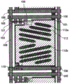
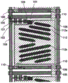
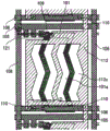
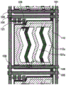
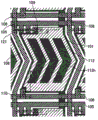
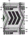
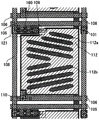
By enlarging the interval between the electrodes that drive the liquid crystal, the gradient of the electric field applied between the electrodes can be controlled, and thus the most suitable electric field can be applied between the electrodes. The technical points of the invention are as follows: the liquid crystal display device includes a first electrode formed over a substrate, an insulating film formed over the substrate and the first electrode, a thin film transistor formed over the insulating film and having a semiconductor film in which a source, a channel region, and a drain are formed, a second electrode located over the semiconductor film and over the first electrode and having a first opening pattern, and liquid crystal disposed over the second electrode.
Description
Technical Field
The present invention relates to a semiconductor device and a liquid crystal display device. The present invention particularly relates to a semiconductor device and a liquid crystal display device in which liquid crystal molecules are controlled by generating an electric field substantially parallel to a substrate.
Background
One of the technical development guidelines of liquid crystal display devices is to enlarge the viewing angle. As a technique for realizing a wide viewing angle, a method of moving liquid crystal molecules in a plane parallel to a substrate by generating an electric field substantially parallel to the substrate to control a gray scale is now adopted. Examples of such a method include IPS (In-Plane switching) and FFS (Fringe-field switching). The FFS can be given as follows: a second electrode having an opening pattern (for example, a pixel electrode in which a voltage is controlled according to each pixel) is disposed under the liquid crystal, and a first electrode (for example, a common voltage is supplied to a common electrode of all pixels) is disposed under the opening pattern. The liquid crystal is controlled by applying an electric field between the pixel electrode and the common electrode. Since an electric field is applied to the liquid crystal in a direction parallel to the substrates, the liquid crystal molecules can be controlled using the electric field. In other words, the liquid crystal molecules aligned parallel to the substrate can be controlled in the direction parallel to the substrate (so-called parallel alignment), and thus the viewing angle can be enlarged.
The first electrode (common electrode) is formed on and in direct contact with the glass substrate, and the gate electrode in the inverted staggered transistor is also formed on and in direct contact with the glass substrate. Over this, an insulating film serving as a gate insulating film in the inverted staggered transistor is formed in direct contact. Further, a second electrode (pixel electrode) is formed thereon (refer to patent document 1).
Alternatively, the first electrode (common electrode) is formed on and in direct contact with an insulating film serving as a gate insulating film in the inverted staggered transistor. Further, the semiconductor film or the source and drain electrodes are also formed over and in direct contact with an insulating film serving as a gate insulating film in the inverted staggered transistor. And on top of that an insulating layer is formed in direct contact. Further, over this, a second electrode (pixel electrode) is formed in direct contact (refer to patent document 1).
Patent document 1 Japanese patent application laid-open No. 2000-89255
In the conventional example as described above, the electrodes for driving the liquid crystal are arranged with an insulating film interposed therebetween. Therefore, there is a limit to increase the distance between the electrodes. If the thickness of the insulating film between the electrodes is increased, for example, the gate insulating film in the transistor is also increased, and thus there is a negative influence such as a decrease in current driving capability of the transistor.
In addition, the optimal value of the arrangement interval of the opening patterns of the pixel electrode or the width of the opening patterns depends on the distance between the pixel electrode and the common electrode. Therefore, when the distance between the pixel electrode and the common electrode cannot be freely set, the arrangement interval of the aperture patterns of the pixel electrode and the value of the width of the aperture patterns are also greatly limited. Therefore, there is a problem that the magnitude of the electric field applied to the liquid crystal molecules or the direction thereof is insufficient.
Disclosure of Invention
In view of the above-described problems, an object of the present invention is to provide a display device and a manufacturing method thereof, in which the degree of freedom of the interval between two electrodes of a display element can be improved, and thus an optimum electric field can be applied between the electrodes.
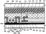
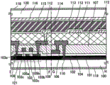
In view of the above problem, a semiconductor device according to the present invention includes: a first electrode formed on the substrate; a first insulating film formed on the first electrode; a semiconductor film formed over the first insulating film; a second insulating film formed over the semiconductor film; a conductive film formed over the second insulating film; a third insulating film formed over the conductive film; and a second electrode formed on the third insulating film and having an opening pattern.
The liquid crystal display device according to the present invention includes: a first electrode formed on the substrate; a first insulating film formed on the first electrode; a semiconductor film formed over the first insulating film; a second insulating film formed over the semiconductor film; a conductive film formed over the second insulating film; a third insulating film formed over the conductive film; a second electrode formed on the third insulating film and having an opening pattern; and a liquid crystal disposed on the second electrode.
According to the semiconductor device and the liquid crystal display device, the first electrode is formed over the substrate, that is, under the semiconductor film. Further, since the second electrode is disposed on a conductive film (for example, a gate electrode, a source electrode, or the like of a transistor) or a third insulating film, the distance between the first electrode and the second electrode can be increased as compared with the conventional art. In addition, even if the thickness of the first insulating film is changed, other elements such as a transistor are not so much affected. Therefore, the thickness thereof can be arbitrarily changed. As a result, the distance between the first electrode and the second electrode can be freely set. Therefore, the degree of freedom of the interval between the first electrode and the second electrode is improved. Also, the gradient of the electric field applied between the electrodes can be controlled, and therefore, for example, the electric field in the direction parallel to the substrate can be easily increased, and the like. In other words, in a display device using liquid crystal, since liquid crystal molecules aligned parallel to a substrate can be controlled in a direction parallel to the substrate (so-called parallel alignment), a viewing angle is widened by applying an optimal electric field.
Further, the opening pattern is used to generate an electric field between the first electrode and the second electrode in a direction substantially parallel to the substrate. Therefore, as long as an electric field in a direction substantially parallel to the substrate can be generated, various shapes can be adopted.
Therefore, as the opening pattern, not only a closed opening pattern of slits or the like but also a space which is located between the conductor patterns and in which the conductor patterns are not formed, for example, a space between comb teeth portions in a comb teeth-shaped electrode or the like can be used. In other words, a gap or space may be formed between the electrodes. The same applies hereinafter.
Another semiconductor device according to the present invention includes: a first electrode formed on the substrate; a first insulating film formed on the first electrode; a semiconductor film formed over the first insulating film; a conductive film formed over the semiconductor film; a second insulating film formed over the conductive film; and a second electrode formed on the second insulating film and having an opening pattern.
According to the semiconductor device and the liquid crystal display device, the first electrode is formed over the substrate, that is, under the semiconductor film. Further, since the second electrode is disposed on a conductive film (e.g., a source electrode) or an insulating film, the distance between the first electrode and the second electrode can be increased as compared with the conventional art. In addition, even if the thickness of the first insulating film is changed, other elements such as a transistor are not so much affected. Therefore, the thickness thereof can be arbitrarily changed. As a result, the distance between the first electrode and the second electrode can be freely set. Therefore, the degree of freedom of the interval between the first electrode and the second electrode is improved. Also, the gradient of the electric field applied between the electrodes can be controlled, so that, for example, the electric field in the direction parallel to the substrate can be easily increased, and so on. In other words, in a display device using liquid crystal, since liquid crystal molecules aligned parallel to a substrate can be controlled in a direction parallel to the substrate (so-called parallel alignment), a viewing angle is widened by applying an optimal electric field.
Another semiconductor device according to the present invention includes: a first electrode formed on the substrate; a first insulating film formed on the first electrode; a conductive film formed over the first insulating film; a semiconductor film formed over the conductive film; a second insulating film formed over the semiconductor film; and a second electrode formed on the second insulating film and having an opening pattern.
According to the semiconductor device and the liquid crystal display device, the first electrode is formed over the substrate, i.e., under the semiconductor film and under a conductive film (e.g., a gate electrode). Further, since the second electrode is disposed on the second insulating film, the distance between the first electrode and the second electrode can be made larger than in the conventional art. In addition, even if the thickness of the second insulating film is changed, other elements such as a transistor are not affected so much. Therefore, the thickness thereof can be arbitrarily changed. As a result, the distance between the first electrode and the second electrode can be freely set. Therefore, the degree of freedom of the interval between the first electrode and the second electrode is improved. Also, the gradient of the electric field applied between the electrodes can be controlled, and therefore, for example, the electric field in the direction parallel to the substrate can be easily increased, and the like. In other words, in a display device using liquid crystal, since liquid crystal molecules aligned parallel to a substrate can be controlled in a direction parallel to the substrate (so-called parallel alignment), a viewing angle is widened by applying an optimal electric field.
As another semiconductor device according to the present invention, in the above structure, the first electrode is a common electrode, and the second electrode is a pixel electrode.
As another semiconductor device according to the present invention, in the above structure, the first electrode is a pixel electrode, and the second electrode is a common electrode.
Another liquid crystal display device according to the present invention includes: a first electrode formed on the substrate; a first insulating film formed on the first electrode; a semiconductor film formed over the first insulating film; a conductive film formed over the semiconductor film; a second insulating film formed over the conductive film; a second electrode formed on the second insulating film and having an opening pattern; and a liquid crystal disposed on the second electrode.
Another liquid crystal display device according to the present invention includes: a first electrode formed on the substrate; a first insulating film formed on the first electrode; a conductive film formed over the first insulating film; a semiconductor film formed over the conductive film; a second insulating film formed over the semiconductor film; a second electrode formed on the second insulating film and having an opening pattern; and a liquid crystal disposed on the second electrode.
As another liquid crystal display device according to the present invention, in the above-described configuration, the liquid crystal is controlled by an electric field between the first electrode and the second electrode.
As another liquid crystal display device according to the present invention, in the above structure, the first electrode is a common electrode and the second electrode is a pixel electrode.
As another liquid crystal display device according to the present invention, in the above structure, the first electrode is a pixel electrode, and the second electrode is a common electrode.
As the switch according to the present invention, various types of switches can be used, and an electric switch, a mechanical switch, and the like are given as examples. In other words, the switch is not limited to a specific one as long as it can control the flow of current, and various switches can be used. For example, a transistor, a diode (e.g., a PN diode, a PIN diode, a schottky diode, a diode-connected transistor, or the like), or a logic circuit combining these may be used. Therefore, in the case where a transistor is used as a switch, since the transistor operates only as a switch, the polarity (conductivity type) of the transistor is not particularly limited. When the off-current is preferably low, a transistor having a polarity with which the off-current is lower is preferably used. As a transistor with a low off-current, a transistor provided with an LDD region or using a multi-gate structure, or the like can be given. In addition, when the transistor used as a switch is operated in a state where the potential of the source terminal is close to the low potential side power source (Vss, GND, OV, or the like), the N-channel type is preferably used, and conversely, when the transistor is operated in a state where the potential of the source terminal is close to the high potential side power source (Vdd or the like), the P-channel type is preferably used. This is because the absolute value of the gate-source voltage can be increased, and thus the switch can be easily operated. Further, a CMOS type switch can be formed by using both an N-channel type and a P-channel type. By employing the CMOS type switch, it is possible to achieve appropriate operation even if the situation changes such as the voltage to be output by the switch (i.e., the input voltage) is high or low with respect to the output voltage. Examples of the switch in the present invention include a TFT for controlling a pixel electrode, a switching element for driving a circuit portion, and the like. But in addition to these portions, a switch may be provided in a portion where it is necessary to control the flow of current.
In the present invention, the connection includes an electrical connection, as well as a direct connection. Therefore, in the structure disclosed in the present invention, other elements (for example, a switch, a transistor, a capacitor, an inductor, a resistor, a diode, or the like) capable of achieving electrical connection between elements may be arranged in addition to the predetermined connection relationship. Alternatively, it may be configured without other elements interposed therebetween. In addition, a case where another element capable of achieving electrical connection is not interposed between the two conductive films and is not electrically connected is referred to as direct connection. Further, when referred to as electrically connected, it includes electrically connected, as well as directly connected.
As the display element, the display device, and the light-emitting device of the present invention, various modes or various elements can be adopted. In the present invention, a liquid crystal element can be used. The liquid crystal element controls transmission or non-transmission of light by utilizing an optical modulation action (optical modulation action) of liquid crystal, and the element is composed of a pair of electrodes and liquid crystal. Examples of a display device using a liquid crystal element include a liquid crystal display, a transmission type liquid crystal display, a transflective type liquid crystal display, and a reflective type liquid crystal display. Further, a display medium whose contrast is changed by an electromagnetic action may be provided, for example, an EL element (an EL element refers to an element having a light-emitting layer capable of obtaining light emission by application of an electric field, and further, an organic EL element, an inorganic EL element, or an EL element containing an organic substance and an inorganic substance, an electron-emitting element, an electronic ink, a grating valve (GLV), a Plasma Display Panel (PDP), a Digital Micromirror Device (DMD), a piezoelectric ceramic display, a carbon nanotube, or the like. Examples of a Display device using an EL element include an EL Display, and examples of a Display device using an Electron-emitting element include an electroluminescence Display (FED) and an SED-type flat-panel Display (SED: Surface-conduction Electron-emitter Display). In addition, as a display device using electronic ink, electronic paper can be given.
In the present invention, various types of transistors can be used as appropriate as the transistor. Therefore, there is no limitation on the kind of transistors that can be applied to the present invention. That is, for example, a Thin Film Transistor (TFT) including a non-single crystal semiconductor film typified by amorphous silicon or polycrystalline silicon, a transistor formed using a semiconductor substrate or an SOI substrate, a MOS transistor, a junction transistor, a bipolar transistor, a transistor using a compound semiconductor such as ZnO or a-InGaZnO, a transistor using an organic semiconductor or a carbon nanotube, or the like can be used as appropriate. In addition, the kind of a substrate over which a transistor is formed is not limited to a specific one, and various substrates can be used. Therefore, the transistor can be formed over, for example, a glass substrate, a plastic substrate, a paper substrate, a cellophane substrate, a stone substrate, or the like. When a reflective display is used, a single crystal substrate or an SOI substrate may be used. Alternatively, a transistor may be formed over a substrate, and then the transistor may be moved over another substrate to be provided over another substrate.
As described above, as the transistor of the present invention, various types can be employed, and can be formed over various substrates. Therefore, all circuits can be formed over a glass substrate or a plastic substrate. In addition, in the case where the manufactured product is a reflective display, the circuit may be formed over a single crystal substrate or an SOI substrate, that is, may be formed over any substrate. By forming all circuits on the same substrate, the number of components can be reduced to reduce cost, and the number of connections with circuit components can be reduced to improve reliability. Alternatively, a part of the circuit may be formed over a substrate and another part of the circuit may be formed over another substrate. In other words, all circuits may not be formed over the same substrate. For example, a part of the circuit may be formed over a Glass substrate using a transistor, and another part of the circuit may be formed over a single crystal substrate, and the IC Chip may be connected to the single crystal substrate by COG (Chip On Glass) and disposed over the Glass substrate. Alternatively, the IC chip and the glass substrate may be connected by TAB (Tape Automated Bonding) or a printed substrate. By forming a part of the circuit over the same substrate in this manner, the number of components can be reduced to reduce cost, and the number of connections to circuit components can be reduced to improve reliability. In addition, since power consumption is high in a portion with a high driving voltage or a portion with a high driving frequency, if the portion is not formed over the same substrate, increase in power consumption can be prevented.
As the structure of the transistor, various modes can be adopted without being limited to a specific structure. For example, a multi-gate structure having two or more gate electrodes may be employed. By adopting the multi-gate structure, off-current can be reduced, withstand voltage of the transistor can be improved to improve reliability, and stable characteristics can be obtained, that is, even if a drain-source voltage changes, a drain-source current does not change so much when operating in a saturation region. Further, a structure in which gate electrodes are disposed above and below the channel may be employed. By adopting a structure in which gate electrodes are disposed above and below a channel, a channel region can be increased, and therefore, a current value can be increased, and an S value can be decreased because a depletion layer is easily generated. In addition, a structure in which the gate electrode is disposed above the channel or a structure in which the gate electrode is disposed below the channel may be employed. In addition, a cross-hatch structure or a reverse cross-hatch structure may be employed. Further, the channel region may be divided into a plurality of regions, or may be connected in parallel or in series. The channel (or a part thereof) may overlap with the source electrode or the drain electrode. By adopting a structure in which the channel (or a part thereof) overlaps with the source electrode or the drain electrode, unstable operation due to accumulation of charges in a part of the channel can be prevented. In addition, an LDD region may be provided. By providing the LDD region, off-current can be reduced, withstand voltage of the transistor can be improved to improve reliability, and stable characteristics can be obtained in which even when a drain-source voltage changes, a drain-source current does not change much when operating in a saturation region.
In the present invention, one pixel refers to one unit capable of controlling luminance. Thus, for example, one pixel refers to one color cell, and the luminance is expressed by the one color cell. Therefore, in the case of employing a color display device configured by color cells of R (red), G (green), and B (blue), the minimum unit of an image is formed by three pixels of an R pixel, a G pixel, and a B pixel. The color elements are not limited to three colors, and more than three colors may be used, such as RGBW (W is white), RGB plus yellow, cyan, magenta, and the like. As another example, in the case where the luminance of one color cell is controlled using a plurality of regions, one of the regions is one pixel. Therefore, as an example, in the case of using the area gray scale method, one color cell has a plurality of regions for controlling luminance, one of which is one pixel, and expresses gray scale by their entirety. Therefore, in this case, one color cell is formed of a plurality of pixels. In addition, in this case, the size of the area contributing to display may be different depending on each pixel. In addition, in a plurality of regions for controlling luminance which one color cell has, that is, in a plurality of pixels constituting one color cell, signals supplied to the respective regions may be slightly different to enlarge a viewing angle. Further, in the case of description as "one pixel (for three colors)", R, G and B three pixels are considered as one pixel; in the case of describing "one pixel (for one color)", when there are a plurality of pixels with respect to each color cell, the plurality of pixels are collected and considered as one pixel.
In the present invention, the pixels may be arranged (arrayed) in a matrix shape. Here, the pixel arrangement (arrangement) in a matrix shape means a case where pixels are arranged in a stripe shape, that is, in a so-called lattice shape in which vertical stripes and horizontal stripes are combined. In addition, when full-color display is performed by three color cells (for example, RGB), dots of the three color cells may be arranged in a so-called triangular shape. Further, the arrangement may be made in a Bayer (Bayer) manner. Further, the color elements are not limited to three colors, and more than three colors may be used, for example, RGBW (W is white), RGB plus yellow, cyan, magenta, and the like. In addition, each color cell may also have a different sized light emitting area.
A transistor is an element having at least three terminals including a gate, a drain, a source, and a channel region provided between a drain region and a source region. Here, the source and the drain of the transistor change depending on the structure, the operating condition, or the like of the transistor, and thus it is not easy to say which is the source or the drain. Therefore, in the present invention, regions functioning as a source and a drain are referred to as a first terminal and a second terminal, respectively.
The gate refers to the whole including a gate electrode and a gate wiring (also referred to as a gate line, a gate signal line, or the like), or to a part of these. The gate electrode is a conductive film which is overlapped with a semiconductor forming a channel region, an LDD (Lightly Doped Drain) region, or the like with a gate insulating film interposed therebetween. The gate wiring is a wiring for connecting gate electrodes of the respective pixels or connecting the gate electrode and another wiring.
Note that there is also a portion functioning as a gate electrode and as a gate wiring. Such a region may be referred to as a gate electrode or a gate wiring. In other words, there is also a region where the gate electrode and the gate wiring cannot be clearly distinguished. For example, when the channel region overlaps with a gate wiring which is arranged to extend, the channel region functions as not only the gate wiring but also the gate electrode. Therefore, such a region may be referred to as a gate electrode or a gate wiring.
In addition, a region which is formed of the same material as the gate electrode and is electrically connected to the gate electrode may be referred to as a gate electrode. Similarly, a region which is formed of the same material as the gate wiring and is electrically connected to the gate wiring may be referred to as a gate wiring. In a strict sense, such a region may not overlap with the channel region or may not have a function of establishing connection with another gate electrode. However, the gate electrode or the gate wiring is made of the same material as the gate electrode or the gate wiring and is electrically connected to the gate electrode or the gate wiring because of reduction in manufacturing cost and steps, simplification of layout, or the like. Therefore, such a region may also be referred to as a gate electrode or a gate wiring.
For example, in a multi-gate transistor, a gate electrode of one transistor is connected to a gate electrode of another transistor in many cases through a conductive film made of the same material as the gate electrode. Such a region is a region for connecting a gate electrode and can be referred to as a gate wiring, but a multi-gate transistor can be regarded as one transistor and can be referred to as a gate electrode. In other words, a gate electrode or a gate wiring which is formed of the same material as the gate electrode or the gate wiring and is electrically connected to the gate electrode or the gate wiring may be referred to as a gate electrode or a gate wiring. For example, a conductive film in a portion connecting a gate electrode and a gate wiring may be referred to as a gate electrode or a gate wiring.
The gate terminal refers to a part of a region of the gate electrode or a region electrically connected to the gate electrode.
The source refers to the whole of a source region, a source electrode, and a source wiring (also referred to as a source line, a source signal line, or the like), or to a part of these. The source region refers to a semiconductor region containing a large amount of P-type impurities (boron, gallium, or the like) or N-type impurities (phosphorus, arsenic, or the like). Therefore, a region slightly containing a P-type impurity or an N-type impurity, that is, a so-called LDD region is not included in the source region. The source electrode is a partial conductive layer made of a material different from that of the source region and arranged to be electrically connected to the source region. Note that the source electrode is sometimes referred to as a source electrode including a source region. The source wiring is a wiring for connecting source electrodes of the respective pixels or connecting the source electrode and another wiring.
However, there is also a portion which functions as a source electrode and as a source wiring. Such a region may be referred to as a source electrode or a source wiring. In other words, there is also a region where the source electrode and the source wiring cannot be clearly distinguished. For example, when a source region overlaps with a source wiring which is arranged to extend, the region serves not only as the source wiring but also as a source electrode. Therefore, such a region may be referred to as a source electrode or a source wiring.
A region which is made of the same material as the source electrode and is electrically connected to the source electrode, or a portion which connects the source electrode and the source electrode may be referred to as a source electrode. The portion overlapping with the source region may also be referred to as a source electrode. Similarly, a region which is made of the same material as the source wiring and is electrically connected to the source wiring may be referred to as a source wiring. To be precise, such a region sometimes does not have a function of making a connection with another source electrode. However, the semiconductor device has a region which is made of the same material as the source electrode or the source wiring and is electrically connected to the source electrode or the source wiring, because of reduction in manufacturing cost and steps, simplification of layout, or the like. Therefore, such a region may also be referred to as a source electrode or a source wiring.
For example, a conductive film in a portion connecting a source electrode and a source wiring may also be referred to as a source electrode or a source wiring.
The source terminal refers to a portion of a region of the source electrode or a region electrically connected to the source electrode.
Further, the drain includes a drain region, a drain electrode, and a drain wiring. In this specification, the term drain is used as in the source. The term drain terminal is also used in the same way as the term source terminal.
In the present invention, a semiconductor device refers to a device having a circuit including a semiconductor element (a transistor, a diode, or the like). In addition, all devices functioning by utilizing semiconductor characteristics may be used. The display device is a device including a display element (a liquid crystal element, a light-emitting element, or the like). The display panel may be a display panel main body in which a plurality of pixels including a display element such as a liquid crystal element or an EL element and a peripheral driver circuit for driving the pixels are formed over a substrate. Further, a display panel mounted with a Flexible Printed Circuit (FPC) or a Printed Wiring Board (PWB) may be included. The light-emitting device is particularly a display device including a self-light-emitting display element such as an EL element or an element used for FED. The liquid crystal display device refers to a display device having a liquid crystal element.
In the present invention, the description of "on" or "on" an object, such as "formed on" or "formed on" an object, is not limited to the case of directly contacting an object. The case where the contact is not direct, that is, the case where another object is sandwiched therebetween is also included. Thus, for example, "the B layer is formed on (or on) the a layer" includes the following two cases: the B layer is formed over the A layer in direct contact; and other layers (e.g., C layer or D layer, etc.) are formed directly in contact over the a layer, and the B layer is formed directly in contact over the other layers. Similarly, the description of "above" is not limited to the case of directly contacting an object, and includes the case of interposing another object therebetween. Thus, for example, "the B layer is formed over the a layer" includes the following two cases: the B layer is formed over the A layer in direct contact; and other layers (e.g., C layer or D layer, etc.) are formed directly in contact over the a layer, and the B layer is formed directly in contact over the other layers. Similarly, the description of "under a certain object" or "under a certain object" includes a case of direct contact and a case of no contact. Here, in the case of being described as being "above a certain object", the side where the electrode is formed is regarded as being above with reference to the substrate where the electrode is formed.
According to the present invention, not only the interval between the first electrode and the second electrode described above can be increased, but also the interval can be controlled without affecting other elements, so that the degree of freedom of the interval is improved. As a result, the arrangement interval of the aperture patterns of the pixel electrode or the optimum value of the width of the aperture patterns depends on the distance between the pixel electrode and the common electrode, and therefore the size of the aperture patterns, the width thereof, and the interval thereof can be freely set. Also, the gradient of the electric field applied between the electrodes can be controlled, so that, for example, the electric field in the direction parallel to the substrate can be easily increased, and so on. In particular, in a display device using liquid crystal, since liquid crystal molecules aligned parallel to a substrate can be controlled in a direction parallel to the substrate (so-called parallel alignment), a viewing angle can be widened by applying an optimal electric field.
Drawings
Fig. 1A is a plan view illustrating a structure of an FFS mode liquid crystal display device according to embodiment 2, and fig. 1B is a sectional view taken along E-F of fig. 1A and a sectional view taken along G-H of fig. 1A;
fig. 2A is a plan view illustrating a structure of an FFS mode liquid crystal display device according to embodiment 2, and fig. 2B is a sectional view taken along E-F of fig. 2A and a sectional view taken along G-H of fig. 2A;
fig. 3A is a plan view illustrating a structure of an FFS mode liquid crystal display device according to embodiment 3, and fig. 3B is a sectional view taken along E-F of fig. 3A and a sectional view taken along G-H of fig. 3A;
fig. 4A is a plan view illustrating a structure of an IPS mode liquid crystal display device according to embodiment 4, and fig. 4B is a sectional view taken along a-B of fig. 4A and a sectional view taken along C-D of fig. 4A;
fig. 5A is a plan view illustrating a structure of an IPS mode liquid crystal display device according to embodiment 5, and fig. 5B is a sectional view taken along a-B of fig. 5A and a sectional view taken along C-D of fig. 5A;
fig. 6A is a plan view illustrating the structure of an FFS mode liquid crystal display device according to embodiment 6, and fig. 6B is a sectional view taken along E-F of fig. 6A and a sectional view taken along G-H of fig. 6A;
fig. 7A is a plan view illustrating the structure of an FFS mode liquid crystal display device according to embodiment 7, and fig. 7B is a sectional view taken along E-F of fig. 7A and a sectional view taken along G-H of fig. 7A;
fig. 8A is a plan view illustrating a structure of an FFS mode liquid crystal display device according to embodiment 8, and fig. 8B is a sectional view taken along E-F of fig. 8A and a sectional view taken along G-H of fig. 8A;
fig. 9A is a plan view illustrating a structure of an FFS mode liquid crystal display device according to embodiment 9, and fig. 9B is a sectional view taken along E-F of fig. 9A and a sectional view taken along G-H of fig. 9A;
fig. 10A is a plan view illustrating the structure of an FFS mode liquid crystal display device according to embodiment 10, and fig. 10B is a sectional view taken along E-F of fig. 10A and a sectional view taken along G-H of fig. 10A;
fig. 11A is a plan view illustrating the structure of an FFS mode liquid crystal display device according to embodiment 11, and fig. 11B is a sectional view taken along E-F of fig. 11A and a sectional view taken along G-H of fig. 11A;
fig. 12A is a plan view illustrating the structure of an FFS mode liquid crystal display device according to embodiment 12, and fig. 12B is a sectional view taken along E-F of fig. 12A and a sectional view taken along G-H of fig. 12A;
fig. 13A is a plan view illustrating the structure of an FFS mode liquid crystal display device according to embodiment 13, and fig. 13B is a sectional view taken along E-F of fig. 13A and a sectional view taken along G-H of fig. 13A;
fig. 14A is a plan view illustrating the structure of an FFS mode liquid crystal display device according to embodiment 14, and fig. 14B is a sectional view taken along E-F of fig. 14A and a sectional view taken along G-H of fig. 14A;
fig. 15A is a plan view illustrating the structure of an FFS mode liquid crystal display device according to embodiment 15, and fig. 15B is a sectional view taken along E-F of fig. 15A and a sectional view taken along G-H of fig. 15A;
fig. 16A is a plan view illustrating the structure of an FFS mode liquid crystal display device according to embodiment 16, and fig. 16B is a sectional view taken along E-F of fig. 16A and a sectional view taken along G-H of fig. 16A;
fig. 17A is a plan view illustrating a structure of an FFS mode liquid crystal display device according to embodiment 17, and fig. 17B is a sectional view taken along E-F of fig. 17A, a sectional view taken along G-H of fig. 17A, and a sectional view taken along I-J of fig. 17A;
fig. 18A is a plan view illustrating the structure of an FFS mode liquid crystal display device according to embodiment 18, and fig. 18B is a sectional view taken along E-F of fig. 18A and a sectional view taken along G-H of fig. 18A;
fig. 19A is a plan view illustrating the structure of an FFS mode liquid crystal display device according to embodiment 19, and fig. 19B is a sectional view taken along I-J of fig. 19A and a sectional view taken along K-L of fig. 19A;
fig. 20A is a plan view illustrating the structure of an FFS mode liquid crystal display device according to embodiment 20, and fig. 20B is a sectional view taken along M-N of fig. 20A and a sectional view taken along O-P of fig. 20A;
fig. 21A is a sectional view illustrating the structure of a liquid crystal display device of the FFS mode according to embodiment 21, and fig. 21B is a sectional view illustrating the structure of a liquid crystal display device of the FFS mode according to embodiment 22;
fig. 22 is a sectional view illustrating the structure of an FFS mode liquid crystal display device according to embodiment 23;
fig. 23 is a sectional view illustrating the structure of a liquid crystal display device according to embodiment 24;
fig. 24A is a plan view of the liquid crystal display device shown in fig. 23, and fig. 24B is an enlarged view of the pixel portion of fig. 24A;
fig. 25A is a plan view of a liquid crystal display device according to embodiment 25, and fig. 25B is an enlarged view of a pixel portion of fig. 25A;
fig. 26 is a sectional view illustrating the structure of a liquid crystal display device according to embodiment 26;
fig. 27A to 27D are plan views illustrating the electrode shape of the FFS mode liquid crystal display device according to embodiment 27;
fig. 28A to 28D are plan views illustrating electrode shapes of an IPS mode liquid crystal display device according to embodiment 28;
fig. 29 is a circuit diagram illustrating a circuit configuration of a liquid crystal display device according to embodiment 29;
fig. 30A and 30B are circuit diagrams illustrating a circuit configuration of a liquid crystal display device according to embodiment 30;
fig. 31A to 31E are sectional views showing a method for manufacturing a liquid crystal module according to embodiment 31;
fig. 32A to 32D are sectional views showing a method for manufacturing a liquid crystal module according to embodiment 31;
fig. 33A is a plan view of a liquid crystal module according to embodiment 31, and fig. 33B is a sectional view cut along K-L of fig. 33A;
fig. 34A and 34B are diagrams illustrating a liquid crystal display module according to embodiment 32;
fig. 35A and 35B are diagrams illustrating a liquid crystal display module according to embodiment 32;
fig. 36A to 36H are oblique views showing an electronic apparatus according to embodiment 33;
fig. 37 is embodiment 1, and is a sectional view illustrating the basic structure of the present invention;
fig. 38A and 38B are sectional views illustrating the structure of a light-emitting device according to embodiment 34.
Detailed Description
Hereinafter, embodiments of the present invention will be described with reference to the accompanying drawings. Note that the present invention can be embodied in many different forms, and those skilled in the art can easily understand the fact that the modes and details thereof can be changed into various forms without departing from the spirit and scope of the present invention. Therefore, the present invention should not be construed as being limited to the description of the embodiment modes.
Embodiment mode 1
Fig. 37 is a sectional view for explaining the basic structure of the present invention. A first electrode 3701 is formed on a substrate 3700. The substrate 3700 is a glass substrate, a quartz substrate, a substrate made of an insulator such as alumina, a heat-resistant plastic substrate, a silicon substrate, or a metal substrate which can withstand the processing temperature of the subsequent process. In the case of using as a transmissive display device, the substrate 3700 preferably has light-transmitting properties.
The first electrode 3701 is formed using a conductive film (e.g., ITO: indium tin oxide) which transmits visible light.
An insulating film 3704 is formed over the substrate 3700 and the first electrode 3701. The insulating film 3704 is made of an insulating substance containing oxygen or nitrogen such as silicon oxide (SiO)x) Silicon nitride (SiN)x) Silicon oxynitride (SiO)xNy: x > y), silicon oxynitride (SiN)xOy: x > y), and the like, and any of these films may be used in a single-layer structure or a stacked-layer structure formed by stacking these films. By providing the insulating film 3704, diffusion of impurities from the substrate 3700 to an upper layer of the insulating film 3704 can be prevented.
Further, a gate electrode, a gate wiring, a gate insulating film, or the like may be provided between the substrate 3700 and the insulating film 3704. In particular, for example, a gate electrode and a gate wiring may be formed by the same step as the first electrode 3701.
A thin film transistor 3703 is formed over the insulating film 3704. The thin film transistor 3703 can be a top gate type transistor or a bottom gate type transistor. The thin film transistor 3703 is disposed in the vicinity of the first electrode 3701 or the second electrode 3702.
An interlayer insulating film 3705 is formed over the thin film transistor 3703 and the insulating film 3704. The interlayer insulating film 3705 may also be a single layer or a multilayer.
As a material constituting the interlayer insulating film 3705, an inorganic material or an organic material can be used. As the organic material, polyimide, acrylic, polyamide, polyimide amide, resist, siloxane, polysilazane, or the like can be used. As the inorganic material, an insulating substance containing oxygen or nitrogen such as silicon oxide (SiO) can be usedx) Silicon nitride (SiN)x) Silicon oxynitride (SiO)xNy: x > y), silicon oxynitride (SiN)xOy: x > y), and the like. Further, a laminated film in which these films are laminated or a laminated film in which an organic material and an inorganic material are combined may be used.
In the case where an inorganic material is used for the interlayer insulating film 3705, intrusion of moisture or impurities can be prevented. Particularly in the case of using a layer containing nitrogen, the barrier ability against moisture or impurities is high. In addition, in the case of using an organic material for the interlayer insulating film 3705, the surface can be made flat. Therefore, it is effective for a layer formed thereon. For example, since a layer formed over an organic material can be made flat, alignment disorder of liquid crystal and disconnection of wiring can be avoided, or a resist can be formed accurately.
A second electrode 3702 is formed on the interlayer insulating film 3705. As the second electrode 3702, a material having high light transmittance, for example, one or more elements selected from the group consisting of indium (In), tin (Sn), and oxygen (O), a compound or an alloy material containing one or more elements selected from the group as its component (for example, Indium Tin Oxide (ITO), Indium Zinc Oxide (IZO), and indium tin oxide to which silicon oxide is added (ITSO)), is preferably used. In particular, IZO is preferably used because IZO is easily processed and a fine and precise shape is easily formed. However, the present invention is not limited thereto.
Any one of the first electrode 3701 and the second electrode 3702 serves as an electrode to which a signal different from each other is supplied according to an image signal to each pixel, that is, a so-called pixel electrode, and is electrically connected to a source electrode or a drain electrode of the thin film transistor 3703. In addition, the remaining one of the first electrode 3701 and the second electrode 3702 serves as a common electrode.
An opening pattern (slit) is formed in the second electrode 3702. The opening pattern is used to generate an electric field between the first electrode 3701 and the second electrode 3702 in a direction substantially parallel to the substrate. The opening pattern may be formed in various shapes as long as an electric field including a direction substantially parallel to the substrate can be generated. Here, substantially parallel means somewhat erroneous parallel. Therefore, the direction may deviate from the parallel direction unless the display is adversely affected. For example, there may be an error of about ± 10 degrees, preferably about ± 5 degrees.
Therefore, as the opening pattern, not only a closed opening pattern of slits or the like but also a space which is located between the conductor patterns and in which the conductor patterns are not formed, for example, a space between comb teeth portions in a comb teeth-shaped electrode or the like can be used. In other words, a gap or space may be formed between the electrodes.
As described above, by generating an electric field between the second electrode 3702 and the first electrode 3701, the alignment state of the liquid crystal molecules can be controlled.
As described above, in this embodiment mode, the insulating film 3704 is formed between the first electrode 3701 and the thin film transistor 3703. Therefore, by adjusting the thickness of the insulating film 3704, the degree of freedom of the interval between the first electrode 3701 and the second electrode 3702 is improved. As a result, the arrangement interval of the aperture patterns of the pixel electrode plate or the optimum value of the width of the aperture patterns depends on the distance between the pixel electrode and the common electrode, and therefore the size of the aperture patterns, the width thereof, and the interval thereof can be freely set. Also, the gradient of the electric field applied between the electrodes can be controlled, so that, for example, the electric field in the direction parallel to the substrate can be easily increased, and so on. In particular, in a display device using liquid crystal, since liquid crystal molecules aligned parallel to a substrate can be controlled in a direction parallel to the substrate (so-called parallel alignment), a viewing angle can be widened by applying an optimal electric field.
Even if the thickness of the insulating film 3704 is changed, the operation of the transistor and the like are not affected, and thus the thickness can be freely controlled. Therefore, the interval between the first electrode 3701 and the second electrode 3702 can be freely enlarged.
In addition, in fig. 37, only the second electrode 3702 is formed to have an opening pattern, but the first electrode 3701 may also have an opening pattern. Therefore, an electric field substantially parallel to the substrate can be generated to control the liquid crystal molecules.
In addition, in the case where the first electrode 3701 is formed, the amount of light transmission is reduced unless the transmittance is 100%. However, in the case where the opening pattern is formed in the first electrode 3701, light is not attenuated in a portion of the opening pattern, and thus the amount of light transmission increases as a whole. As a result, the luminance can be improved or the power consumption can be reduced.
Embodiment mode 2
Fig. 1A is a plan view illustrating the structure of a liquid crystal display device according to embodiment 2 of the present invention, which shows one pixel. The liquid crystal display device is a device for controlling the orientation of liquid crystal in an FFS manner. In fig. 1A, the plurality of source wirings 108 are arranged in parallel with each other (extending in the longitudinal direction in the drawing) and separated from each other. The plurality of gate wirings 105 are arranged to extend in a direction (in the drawing, a lateral direction) substantially orthogonal to the source wiring 108 and to be separated from each other. The supplemental wiring 106 is disposed at a position close to each of the plurality of gate wirings 105, and extends in a direction substantially parallel to the gate wirings 105, that is, in a direction substantially orthogonal to the source wiring 108 (in the drawing, the left-right direction). A space substantially similar to a rectangular shape is surrounded by the source wiring 108, the complementary wiring 106, and the gate wiring 105, and a pixel electrode of the liquid crystal display device is arranged in the space. A thin film transistor 121 that drives the pixel electrode is disposed in the upper left corner of the drawing. The plurality of pixel electrodes and the thin film transistors are arranged in a matrix shape.
Further, the gate wiring 105, the complementary wiring 106, and the source wiring 108 are formed of the following materials: one or more elements selected from the group consisting of aluminum (Al), tantalum (Ta), titanium (Ti), molybdenum (Mo), tungsten (W), neodymium (Nd), chromium (Cr), nickel (Ni), platinum (Pt), gold (Au), silver (Ag), copper (Cu), magnesium (Mg), scandium (Sc), cobalt (Co), zinc (Zn), niobium (Nb), silicon (Si), phosphorus (P), boron (B), arsenic (As), gallium (Ga), indium (In), tin (Sn), and oxygen (O); a compound or an alloy material containing one or more elements selected from the group (for example, Indium Tin Oxide (ITO), Indium Zinc Oxide (IZO), indium tin oxide to which silicon oxide is added (ITSO), zinc oxide (ZnO), aluminum neodymium (Al-Nd), magnesium silver (Mg-Ag), or the like); a combination of these compounds, and the like. Or compounds (silicides) of these with silicon (e.g., aluminum silicon, molybdenum silicon, nickel silicide, etc.), or compounds (e.g., titanium nitride, tantalum nitride, molybdenum nitride, etc.) of these with nitrogen. Silicon (Si) may contain a large amount of n-type impurities (phosphorus, etc.) or P-type impurities (boron, etc.). When these impurities are included, the conductivity is improved, and the same function as that of a general conductor is exerted, so that the conductive material can be easily used as a wiring or an electrode. Further, the silicon may be single crystal, polycrystalline (polysilicon), or amorphous (amorphous silicon). By using single crystal silicon or polycrystalline silicon, resistance can be reduced. By using amorphous silicon, the manufacturing process can be simplified. As for aluminum or silver, it has high conductivity, so that signal delay can be reduced, and since it is easily etched, it is easily processed and can be finely processed. As for copper, its conductivity is high, and thus signal delay can be reduced. Further, molybdenum is preferably used because it does not cause problems such as material defects even when it is in contact with an oxide semiconductor such as ITO or IZO or silicon, and because molybdenum is easily processed and etched and has high heat resistance. Further, titanium is preferably used because it does not cause problems such as material defects even when titanium is in contact with an oxide semiconductor such as ITO or IZO, or silicon, and has high heat resistance. Further, tungsten is preferably used because of its high heat resistance. Further, neodymium is preferably used because of its high heat resistance. In particular, an alloy of neodymium and aluminum is preferably used because its heat resistance is improved and hillocks are less likely to be generated in aluminum. Further, since silicon can be formed at the same time as a semiconductor film included in a transistor and heat resistance is high, silicon is preferably used. In addition, Indium Tin Oxide (ITO), Indium Zinc Oxide (IZO), indium tin oxide to which silicon oxide is added (ITSO), zinc oxide (ZnO), and silicon (Si) are preferably used because they have light-transmitting properties and thus can be suitably used for a portion that transmits light. For example, they are used as pixel electrodes or common electrodes.
The wiring or the electrode may be formed of a single layer or a stacked layer of the above materials. By adopting the single-layer structure, the manufacturing process can be simplified and the number of manufacturing days can be reduced, leading to a reduction in cost. On the other hand, when a multilayer structure is employed, advantages of various materials can be used and disadvantages thereof can be reduced, thereby forming a high-performance wiring or electrode. For example, by including a low-resistance material (e.g., aluminum) in the multilayer structure, the resistance of the wiring can be reduced. In addition, by including a high heat-resistant material, for example, when a stacked-layer structure in which a material which does not have high heat resistance but has other advantages is interposed between the high heat-resistant materials is employed, heat resistance of the wiring or the electrode as a whole can be improved. For example, a stacked-layer structure in which a layer containing aluminum is interposed between layers containing molybdenum or titanium is preferably used. In addition, if a wiring or an electrode is in direct contact with another wiring or an electrode or the like made of a different material, they may adversely affect each other. For example, the material of one wiring or electrode may enter into the other wiring or electrode to change its properties, thereby failing to achieve the intended purpose, or a problem occurs in manufacturing and the manufacturing process cannot be completed normally. In this case, the problem can be solved by inserting another layer or covering it with it. For example, in the case where Indium Tin Oxide (ITO) is in contact with aluminum, titanium or molybdenum is preferably interposed therebetween. In the case where silicon is in contact with aluminum, titanium or molybdenum is preferably interposed therebetween.
Further, the gate wiring 105 is preferably formed using a material having higher heat resistance than the source wiring 108. This is because the gate wiring 105 is often in a high temperature state in the manufacturing process compared to the source wiring 108.
Further, the source wiring 108 is preferably formed using a material having lower resistance than the gate wiring 105. This is because, although only two-valued signals, i.e., an H signal and an L signal, are supplied to the gate wiring 105, an analog signal is supplied to the source wiring 108, which contributes to display. Therefore, it is preferable to form the source wiring 108 using a low-resistance material to supply a signal of a correct size.
Further, the supplementary wiring 106 may not be provided, but by providing the supplementary wiring 106, the potential of the common electrode in each pixel can be stabilized. Further, in fig. 1A and 1B, the supplemental wiring 106 is arranged substantially in parallel with the gate line, but the present invention is not limited thereto. The supplemental wiring 106 may also be arranged substantially parallel to the source wiring 108. In this case, the supplemental wiring 106 is preferably made of the same material as the source wiring 108.
However, the supplemental wiring 106 is preferably arranged substantially parallel to the gate line because the aperture ratio can be improved and the layout can be efficiently performed.
FIG. 1B is a cross-sectional view taken along E-F of FIG. 1A and a cross-sectional view taken along G-H of FIG. 1A. As shown in fig. 1A and 1B, a first electrode 101 for controlling the alignment of liquid crystals is provided on a part of a substrate 100. However, another layer may be provided between the substrate 100 and the first electrode 101.
The substrate 100 is a glass substrate, a quartz substrate, a substrate made of an insulator such as alumina, a heat-resistant plastic substrate, a silicon substrate, or a metal substrate which can withstand the processing temperature of the subsequent process. Alternatively, it may be polysilicon.
In the case of using as a transmissive display device, the substrate 100 preferably has light-transmitting properties.
The first electrode 101 is formed of a conductive film having light transmittance (e.g., an ITO (indium tin oxide) film, an IZO (indium zinc oxide) film, a ZnO film, or a polycrystalline silicon film doped with impurities or an amorphous silicon film), and functions as a common electrode. Further, as shown in fig. 1A, the first electrodes 101 are connected in the up-down direction. By connecting the first electrodes 101 in the vertical direction, the resistance of the common electrode can be reduced, and a predetermined voltage can be easily applied.
An insulating film 102 is formed over the first electrode 101 and the substrate 100. The insulating film 102 is a film which prevents diffusion of impurities from the substrate 100, and functions as a base film. The insulating film 102 is made of an insulating substance containing oxygen or nitrogen such as silicon oxide (SiO)x) Silicon nitride (SiN)x) Silicon oxynitride (SiO)xNy: x > y), silicon oxynitride (SiN)xOy: x > y), and the like, and a laminated film formed by laminating these films can be used. An insulating film which functions similarly to the insulating film 102 may be formed between the substrate 100 and the first electrode 101.
A semiconductor film 103 is formed on the insulating film 102. An impurity region 103a functioning as a source and an impurity region 103b functioning as a drain of the thin film transistor 121 are formed in the semiconductor film 103. The impurity regions 103a and 103b are, for example, n-type impurity regions, but may be p-type impurity regions. Examples of the n-type-imparting impurity include phosphorus (P) and arsenic (As). Examples of the impurity imparting p-type conductivity include boron (B) and gallium (Ga).
As shown by a broken line in fig. 1A, the first electrode 101 has a shape lacking one corner of its rectangle (upper left corner in the drawing), and is formed over substantially the entire face of the pixel. In addition, a thin film transistor 121 is disposed in a portion 101d where one corner of the rectangle is absent. By disposing the thin film transistor 121 in the portion 101d lacking a corner, an area effective for display in a pixel is formed more efficiently. In other words, the aperture ratio can be improved. The semiconductor film 103 is, for example, a polysilicon film, but may be another semiconductor film (for example, an amorphous silicon film, a single crystal silicon film, an organic semiconductor film, or a carbon nanotube).
A gate insulating film 104 of a thin film transistor 121 is formed so as to cover the semiconductor film 103.
Note that the gate insulating film 104 may be formed only in the vicinity of the channel region, and not formed in other portions. In addition, the gate insulating film 104 may partially have different thicknesses and a stacked-layer structure. For example, the thickness is large and the number of layers is large only in the vicinity of the channel, and the thickness is small and the number of layers is small in other portions. With this structure, the impurity addition to the source region or the drain region can be easily controlled. In addition, by changing the thickness or the number of layers of the gate insulating film 104 located in the vicinity of the channel, the amount of impurity addition to the semiconductor film can be partially made different to form an LDD region. By forming the LDD region, leakage current can be reduced, and generation of hot carriers can be suppressed to improve reliability.
The gate insulating film 104 is made of an insulating substance containing oxygen or nitrogen such as silicon oxide (SiO)x) Silicon nitride (SiN)x) Silicon oxynitride (SiO)xNy: x > y), silicon oxynitride (SiN)xOy: x > y), and the like. Further, a laminated film formed by laminating these films may be used. Gate electrodes 105a and 105b are formed over the semiconductor film 103 on the gate insulating film 104. As shown in fig. 1A and 1B, the gate electrodes 105a and 105B are the same wiring layer as the complementary wiring 106 and the gate wiring 105, and are electrically connected to the gate wiring 105. The semiconductor film 103 located under the gate electrodes 105a and 105b serves as a channel region 103 c. In addition, the same impurity as the impurity regions 103a and 103b is added to the semiconductor film 103 located between the two channel regions 103 c. Further, in this embodiment mode, a multi-gate structure having two gate electrodes is employed, but the present invention is not limited to such a structure.
A first interlayer insulating film 107 is formed over the gate insulating film 104 and the gate electrodes 105a and 105 b. The first interlayer insulating film 107 may be formed using an inorganic material or an organic material. As the organic material, polyimide, acrylic, polyamide, polyimide amide, resist, siloxane, polysilazane, or the like can be used. As the inorganic material, an insulating substance containing oxygen or nitrogen such as silicon oxide (SiO) can be usedx) Silicon nitride (SiN)x) Silicon oxynitride (SiO)xNy: x > y), silicon oxynitride (SiN)xOy: x > y), and the like. Further, a laminated film in which these films are laminated or a laminated film in which an organic material and an inorganic material are combined may be used. The insulating film 102, the gate insulating film 104, and the first interlayer insulating film 107 have a connection formed thereon over the impurity region 103aA hole, a connection hole located on the impurity region 103b, a connection hole located on the first electrode 101, and a connection hole located on the complementary wiring 106. A source wiring 108, a conductive film 109 for connection, and a conductive film 110 for connection are formed on the first interlayer insulating film 107.
Further, by using an inorganic material as the insulating film, intrusion of moisture or impurities can be prevented. Particularly in the case of using a layer containing nitrogen, the barrier ability against moisture or impurities is high.
Further, by using an organic material as the insulating film, the surface can be made flat. Therefore, it is effective for a layer formed thereon. For example, a layer formed over an organic material can be made flat, and thus alignment disorder of liquid crystal can be avoided.
The source wiring 108 is located on the impurity region 103a, and a part thereof is embedded in the connection hole to be electrically connected to the impurity region 103 a. Therefore, a part of the source wiring 108 is a source electrode. As for the conductive film 109 for connection, a part thereof is embedded in the connection hole to be electrically connected to the impurity region 103 b. By disposing the conductive film for connection 109 in this manner, it is not necessary to make the connection hole deep, and therefore, the conductive film can be formed accurately.
Note that as shown in fig. 2B, the second electrode 112 and the impurity region 103B may be directly connected without interposing the conductive film 109 for connection shown in fig. 1B therebetween. In this case, although it is necessary to use a deep connection hole for connecting the second electrode 112 and the impurity region 103b, the conductive film 109 for connection is not necessary, and thus the region can be used for image display with the region being an opening region. Therefore, the aperture ratio can be increased, and power consumption can be reduced.
The conductive film for connection 110 is located on the complementary wiring 106, and a part thereof is embedded in the connection hole and electrically connected to the complementary wiring 106 and the first electrode 101, respectively. In this manner, the first electrode 101 is electrically connected to the complementary wiring 106 with the conductive film for connection 110 interposed therebetween. Further, a plurality of conductive films 110 for connection may be provided. By adopting such a structure, the potential of the first electrode 101 can be stabilized. In addition, the first electrode 101 and the complementary wiring 106 are connected with the conductive film for connection 110 interposed therebetween, and the number of times of forming a connection hole can be reduced, so that the manufacturing process can be simplified.
Here, the conductive film 110 for connection is formed using the same material as the source wiring 108, but the present invention is not limited thereto. The conductive film for connection 110 may be formed using the same material as the second electrode 112.
A second interlayer insulating film 111 is formed over the source wiring 108, the conductive film 109 for connection, the conductive film 110 for connection, and the first interlayer insulating film 107. Further, the second interlayer insulating film 111 may not be formed. The second interlayer insulating film 111 may be formed using an inorganic material or an organic material. As the organic material, polyimide, acrylic, polyamide, polyimide amide, resist, siloxane, polysilazane, or the like can be used. As the inorganic material, an insulating substance containing oxygen or nitrogen such as silicon oxide (SiO) can be usedx) Silicon nitride (SiN)x) Silicon oxynitride (SiO)xNy: x > y), silicon oxynitride (SiN)xOy: x > y), and the like. Further, a laminated film in which these films are laminated or a laminated film in which an organic material and an inorganic material are combined may be used. A connection hole located above the connection conductive film 109 is formed in the second interlayer insulating film 111.
A second electrode 112 for controlling the orientation of the liquid crystal is formed on the second interlayer insulating film 111. The second electrode 112 serves as a pixel electrode to which a voltage is supplied to each pixel, respectively, and is composed of: ITO (indium tin oxide), ZnO (zinc oxide), IZO (indium zinc oxide) formed by using a target in which ZnO of 2 to 20 wt% is mixed into indium oxide, and the like. A part of the second electrode 112 is located on the conductive film for connection 109, and a part of the part is embedded in the connection hole to be electrically connected to the conductive film for connection 109. In this manner, the second electrode 112 is electrically connected to the impurity region 103b of the thin film transistor 121 with the conductive film for connection 109 interposed therebetween.
Further, as shown in fig. 2A and 2B, in the case where the conductive film 109 for connection is not formed, the second electrode 112 is directly connected to the impurity region 103B of the thin film transistor 121.
As shown in fig. 2A and 2B and fig. 1A, the second electrode 112 is substantially rectangular and is located above the first electrode 101, and the second electrode 112 has a plurality of opening patterns 112A and 112B. As an example of the opening patterns 112a and 112b, a shape in which a plurality of slits are parallel to each other may be given. In the example shown in the figure, the opening patterns 112a and 112b are inclined with respect to the source wiring 108, and the directions of the opening pattern 112a located in the upper half of the pixel in the figure and the opening pattern 112b located in the lower half of the figure are different from each other. By forming the opening patterns 112a and 112b, an electric field having a composition parallel to the substrate between the first electrode 101 and the second electrode 112 is generated on the second electrode 112. Therefore, by controlling the potential of the second electrode 112, the alignment of the liquid crystal as described below can be controlled.
Further, by making the directions of the opening patterns different from each other like the opening patterns 112a and 112b, a plurality of regions in which the moving direction of the liquid crystal molecules is different can be provided. In other words, a multi-domain structure may be employed. By adopting the multi-domain structure, abnormal display of an image when viewed in a certain direction can be prevented, and as a result, the viewing angle can be improved.
The shape of the opening pattern is not limited to the shape of the present embodiment. The shape of the opening pattern described later in embodiment 3 can also be adopted. In other words, as the opening pattern, a space in which the conductor pattern is not formed, for example, a space between comb-teeth portions in the comb-teeth-shaped electrode, or the like can be used.
In addition, as shown in fig. 1A, the first electrode 101 serving as a common electrode extends to the outside of the second electrode 112 serving as a pixel electrode when viewed in a direction perpendicular to the substrate 100. With such a structure, it is possible to suppress a signal transmitted to another pixel through the source wiring 108 from affecting the second electrode 112 which becomes a floating state after receiving the signal. As a result, image defects such as crosstalk and the like can be reduced. The present invention is not limited to this electrode structure, and the common electrode may be disposed inside the pixel electrode.
A first alignment film 113 and a liquid crystal 114 are stacked on the second interlayer insulating film 111 and the second electrode 112. As the liquid crystal 114, Ferroelectric Liquid Crystal (FLC), nematic liquid crystal, smectic liquid crystal, liquid crystal in parallel alignment, liquid crystal in vertical alignment, or the like can be used. A counter substrate 120 is disposed on the liquid crystal 114 with the second alignment film 115 and the color filter 116 interposed therebetween. Further, the substrate 100 and the opposite substrate 120 are provided with polarizing plates 119 and 118, respectively.
In addition to the polarizing plate, a retardation plate, a λ/4 plate, or the like is often disposed.
In the above-described structure, the first electrode 101, the second electrode 112, portions where the opening patterns are not formed, and the respective insulating films located therebetween form a capacitor. By forming the capacitance, the holding capacitance can be increased.
Next, an example of a method for manufacturing a semiconductor device and a liquid crystal display device according to the present invention will be described. First, a conductive film having light-transmitting properties (e.g., an ITO (indium tin oxide) film, an IZO film, a ZnO film, or a Si film) is formed over the substrate 100. Then, a photoresist film (not shown) is formed on the conductive film, and the photoresist film is exposed and developed. Thus, a resist pattern is formed on the conductive film. Then, the conductive film is etched using the resist pattern as a mask. By performing such processing, the conductive film is selectively removed to form the first electrode 101 over the substrate 100. Then, the resist pattern is removed.
Next, an insulating film 102 is formed over the substrate 100 and the first electrode 101. The insulating film 102 is preferably thicker than a gate insulating film 104 described below. Then, a semiconductor film (e.g., a polysilicon film) is formed on the insulating film 102, and etching using a resist pattern is performed to selectively remove the semiconductor film. Thus, the island-shaped semiconductor film 103 is formed on the insulating film 102.
Next, a gate insulating film 104 is formed over the semiconductor film 103 and the insulating film 102. The gate insulating film 104 is, for example, a silicon oxynitride film or a silicon oxide film, and is formed by a plasma CVD method. The gate insulating film 104 may be formed of a silicon nitride film or a multilayer film including silicon nitride and silicon oxide. Next, a conductive film is formed over the gate insulating film 104, and is selectively removed by etching using the resist pattern as a mask. Thus, gate electrodes 105a and 105b are formed on the gate insulating film 104 located on the semiconductor film 103. By performing such a step, the gate wiring 105 and the complementary wiring 106 are formed.
Further, as described above, by forming the supplemental wiring 106, the potential of the first electrode 101 can be stabilized in each pixel. In addition, the supplementary wiring 106 may not be formed. The supplemental wiring 106 may be formed in another layer (for example, the same layer as the source wiring 108, the same layer as the first electrode 101, or the same layer as the second electrode 112), or may be formed in a plurality of layers. In fig. 1B, the supplemental wiring 106 extends in a direction orthogonal to the source wiring 108, but the supplemental wiring 106 may extend in the same direction as the source wiring 108.
Further, the conductive film is composed of: one or more elements selected from the group consisting of aluminum (Al), tantalum (Ta), titanium (Ti), molybdenum (Mo), tungsten (W), neodymium (Nd), chromium (Cr), nickel (Ni), platinum (Pt), gold (Au), silver (Ag), copper (Cu), magnesium (Mg), scandium (Sc), cobalt (Co), zinc (Zn), niobium (Nb), silicon (Si), phosphorus (P), boron (B), arsenic (As), gallium (Ga), indium (In), tin (Sn), and oxygen (O); a compound or an alloy material containing one or more elements selected from the group (for example, Indium Tin Oxide (ITO), Indium Zinc Oxide (IZO), indium tin oxide to which silicon oxide is added (ITSO), zinc oxide (ZnO), aluminum neodymium (Al-Nd), magnesium silver (Mg-Ag), or the like); a combination of these compounds, and the like. Or compounds (silicides) of these with silicon (e.g., aluminum silicon, molybdenum silicon, nickel silicide, etc.), or compounds (e.g., titanium nitride, tantalum nitride, molybdenum nitride, etc.) of these with nitrogen. Silicon (Si) may contain a large amount of n-type impurities (phosphorus, etc.) or P-type impurities (boron, etc.).
The wiring or the electrode may be formed of a single layer or a stacked layer of the above materials. By adopting the single-layer structure, the manufacturing process can be simplified and the number of manufacturing days can be reduced, leading to a reduction in cost. On the other hand, when a multilayer structure is employed, advantages of various materials can be used and disadvantages thereof can be reduced, thereby forming a high-performance wiring or electrode. For example, by including a low-resistance material (e.g., aluminum) in the multilayer structure, the resistance of the wiring can be reduced. In addition, by including a high heat-resistant material, for example, when a stacked-layer structure in which a material which does not have high heat resistance but has other advantages is interposed between the high heat-resistant materials is employed, heat resistance of the wiring or the electrode as a whole can be improved. For example, a stacked-layer structure in which a layer containing aluminum is interposed between layers containing molybdenum or titanium is preferably used. In addition, in the case of having a portion which is in direct contact with a wiring or an electrode or the like of other material, they may adversely affect each other. For example, the material of one wiring or electrode may enter the material of the other wiring or electrode to change its properties, thereby failing to achieve the intended purpose, or a problem occurs in manufacturing and the manufacturing process cannot be completed normally. In this case, the problem can be solved by inserting another layer or covering it with it. For example, in the case where Indium Tin Oxide (ITO) is in contact with aluminum, titanium or molybdenum is preferably interposed therebetween. In the case where silicon is in contact with aluminum, titanium or molybdenum is preferably interposed therebetween.
Next, an impurity is added to the semiconductor film 103 with the gate electrodes 105a and 105b as masks. Therefore, the impurity regions 103a and 103b and the impurity region between the gate electrodes 105a and 105b are formed in the semiconductor film 103. Further, an n-type impurity element and a p-type impurity element may be added separately, or an n-type impurity element and a p-type impurity element may be added together in a specific region. Note that in the latter case, the amount of addition of any one of the n-type impurity element and the p-type impurity element is set to be larger than that of the other. In this step, a resist pattern may be used as a mask.
At this time, the LDD region may be formed by changing the thickness or the stacked structure of the gate insulating film 104. The portion where an LDD region is to be formed may be formed by making the gate insulating film 104 thick or increasing the number of layers. As a result, the amount of impurity added is reduced, and therefore, the LDD region can be easily formed.
Further, in the case where an impurity is added to the semiconductor film 103, the impurity may be added before the gate electrodes 105a and 105b are formed, for example, before or after the gate insulating film 104 is formed. In this case, the resist pattern is used as a mask. Therefore, capacitance can be formed between the electrode formed in the same layer as the gate electrode and the semiconductor film to which the impurity is added. Since the gate insulating film is formed between the electrode in the same layer as the gate electrode and the semiconductor film to which the impurity is added, a large capacitance with a small thickness can be formed.
Next, the first interlayer insulating film 107 and the respective connection holes are formed. Then, a conductive film (e.g., a metal film) is formed over the first interlayer insulating film 107 and in each connection hole, and etching using a resist pattern is performed to selectively remove the conductive film. Thus, the source wiring 108, the conductive film 109 for connection, and the conductive film 110 for connection are formed.
Next, the second interlayer insulating film 111 and the connection holes are formed. Then, a conductive film having light transmittance (e.g., an ITO film, an IZO film, a ZnO film, or a Si film) is formed on the second interlayer insulating film 111 and in each connection hole, and the conductive film is selectively removed by etching using a resist pattern. Thus, the second electrode 112 is formed.
Further, the positions of the connection hole in which a part of the conductive film 109 for connection is embedded and the connection hole in which a part of the second electrode 112 is embedded are different from each other. By adopting such a structure, even if portions of the conductive film for connection 109 and the second electrode 112 which are located above the connection hole are recessed, the recessed portions do not overlap. Accordingly, a deep concave portion is not formed in the second electrode 112, and thus a defect of the resist pattern can be suppressed. Then, the resist pattern is removed.
Next, the first alignment film 113 is formed, and the liquid crystal 114 is sealed between the counter substrate 120 on which the second alignment film 115 is formed. Then, polarizing plates 118 and 119, optical films (not shown) such as a retardation plate (not shown) and a λ/4 plate, optical films such as a diffusion plate and a prism plate, and the like are formed on the counter substrate 120 or the substrate 100 on the side not in contact with the liquid crystal 114. Furthermore, a backlight or a frontlight is also provided. As the backlight, a direct type or a side light type can be employed. As the light source, a cold cathode tube or an LED (light emitting diode) may be used. As the LED, a white LED may be used, or LEDs of respective colors (for example, white, red, blue, green, cyan, magenta, yellow, and the like) may be combined. By using the LED, since the wavelength peak of light is sharp, the color purity can be improved. In the case of the side light type, a light guide plate is disposed to realize a uniform surface light source. In this manner, a liquid crystal display device is formed.
Further, the liquid crystal display device may mean only a substrate, an opposite substrate, and a portion of liquid crystal sandwiched therebetween. Further, as the liquid crystal display device, an optical film such as a polarizing plate or a retardation plate may be disposed. In addition, a diffusion plate, a prism plate, a light source (cold cathode tube, LED, or the like), a light guide plate, or the like may be included.
As described above, according to embodiment 2 of the present invention, in the liquid crystal display device in which the alignment of liquid crystal is controlled in the FFS mode, the first electrode 101 is disposed on the substrate 100, that is, under the insulating film 102. Therefore, the interval between the first electrode 101 and the second electrode 112 can be increased as compared with the case where the first electrode 101 is formed on the insulating film 102. Therefore, the degree of freedom of the interval between the first electrode 101 and the second electrode 112 is improved. As a result, the arrangement interval of the aperture patterns of the pixel electrode or the optimum value of the width of the aperture patterns depends on the distance between the pixel electrode and the common electrode, and therefore the size of the aperture patterns, the width thereof, and the interval thereof can be freely set. Also, the gradient of the electric field applied between the electrodes can be controlled, and therefore, for example, the electric field in the direction parallel to the substrate can be easily increased, and the like. In other words, in a display device using liquid crystal, since liquid crystal molecules aligned parallel to a substrate can be controlled in a direction parallel to the substrate (so-called parallel alignment), a viewing angle is widened by applying an optimal electric field.
Even if the thickness of the insulating film 102 is changed, the operation of the transistor and the like are not affected, and thus the thickness can be freely controlled. Therefore, the interval between the first electrode 101 and the second electrode 112 can be freely enlarged.
By making the insulating film 102 thick, the interval between the first electrode 101 and the second electrode 112 is increased even if the gate insulating film 104 is made thin, and an appropriate electric field is applied to the liquid crystal 114. In the case where the gate insulating film 104 is made thin, the current driving capability of the thin film transistor 121 can be improved, and the gate capacitance can be improved.
In addition, the gate electrode 105a and the gate wiring 105 may be formed in different layers, or the gate electrode 105a and the gate wiring 105 may be formed using different materials.
The conductive film 109 for connection is provided in the same layer as the source wiring 108, but may be provided in another wiring layer (for example, the same layer as the gate wiring 105, the first electrode 101, or the second electrode 112). The gate insulating film 104 may not be formed over the entire surface.
In addition, a connection hole into which a part of the second electrode 112 is embedded may be formed at a position overlapping with a connection hole into which a part of the conductive film 109 for connection is embedded. In this case, since two connection holes can be formed in one region, layout can be efficiently performed. Therefore, the aperture ratio of the pixel can be improved.
In this embodiment, a so-called top-gate thin film transistor in which a gate electrode is provided over a channel region is described, but the present invention is not limited to this. A so-called bottom gate thin film transistor in which a gate electrode is provided below a channel region, or a thin film transistor in which a gate electrode is provided above and below a channel region may be used.
The liquid crystal display device may be a transmission type liquid crystal display device, a semi-transmission type or a reflection type liquid crystal display device. The semi-transmissive type liquid crystal display device is realized by, for example, forming the first electrode 101 using a light-transmitting film such as an ITO (indium tin oxide) film, an IZO (indium zinc oxide) film, a ZnO film, or a polysilicon film added with impurities or an amorphous silicon film, and forming the second electrode 112 using a metal film. In addition, the second electrode 112 may be formed using a light-transmitting film, and a part of the first electrode 101 may be formed using a metal film and another part of the first electrode 101 may be formed using a light-transmitting film, so that a transflective liquid crystal display device may be implemented. In addition, in the reflective liquid crystal display device, by using a metal film as the first electrode 101, the first electrode 101 can function as a reflective plate. In addition, an insulating film (e.g., a silicon oxide film) may be formed between the substrate 100 and the first electrode 101 to form a metal film as a reflective film in the insulating film. Further, a reflective sheet (e.g., an aluminum film) may be provided as a reflective film on the outer surface of the substrate 100. Note that the contents described here can be similarly applied to the following embodiments.
Embodiment 3
Fig. 3A is a plan view illustrating the structure of a liquid crystal display device according to embodiment 3, and fig. 3B is a sectional view taken along E-F of fig. 3A and a sectional view taken along G-H of fig. 3A. The configuration of the present embodiment is substantially the same as embodiment 2, and differs from embodiment 2 in the following points: the first electrode 101 is electrically connected to the impurity region 103b of the thin film transistor 121 and functions as a pixel electrode; the second electrode 112 is electrically connected to the supplemental wiring 106, and functions as a common electrode; the second electrode 112 extends to the outside of the first electrode 101 when viewed in the direction perpendicular to the substrate 100; and a connection structure of the first electrode 101 and the second electrode 112 to each wiring. The method for manufacturing the liquid crystal display device according to this embodiment is substantially the same as that of embodiment 2. Therefore, the contents described in embodiment 2 can be applied to this embodiment as well. Hereinafter, the same reference numerals are used to designate the same components as those in embodiment 2, and the description thereof will be omitted.
In this embodiment mode, a connection hole located above the first electrode 101 is formed in the first interlayer insulating film 107, the gate insulating film 104, and the insulating film 102, and a connection hole located above the impurity regions 103a and 103b of the thin film transistor 121 is formed in the first interlayer insulating film 107 and the gate insulating film 104. In addition, a connection hole located above the complementary wiring 106 is formed in the first interlayer insulating film 107.
The conductive film for connection 109 extends from the impurity region 103b to the first electrode 101, and a part thereof is embedded in a connection hole to be electrically connected to the impurity region 103b and the first electrode 101, respectively. In this manner, the first electrode 101 is electrically connected to the impurity region 103b through the conductive film for connection 109. In addition, a part of the conductive film for connection 110 is embedded in the connection hole and electrically connected to the complementary wiring 106.
The first electrode 101 may be electrically connected to the impurity region 103b through a conductive film for connection formed in the same layer as the second electrode 112.
A connection hole located above the conductive film for connection 110 is formed in the second interlayer insulating film 111. As for the second electrode 112, a part thereof is embedded in the connection hole and electrically connected to the conductive film for connection 110. In this manner, the second electrode 112 is electrically connected to the complementary wiring 106 through the conductive film for connection 110. Further, as shown in fig. 3A, the upper and lower second electrode 112 portions are connected to each other.
Further, the supplemental wiring 106 and the second electrode 112 may be directly connected without disposing the conductive film 110 for connection.
In this embodiment, the conductive films 110 for connection are formed at three corners, except for the corner located near the thin film transistor, among the four corners of the first electrode 101.
According to this embodiment, the same effects as those of embodiment 2 can be obtained. In this embodiment, the conductive film for connection 110 may not be provided. In this case, a connection hole located on the complementary wiring 106 is formed in the first and second interlayer insulating films 107 and 111. By embedding a part of the second electrode 112 in the connection hole, the supplemental wiring 106 and the second electrode 112 are electrically connected. In this case, the aperture ratio can be improved. However, in the case where the conductive film for connection 110 is provided, even if the connection holes formed in the first and second interlayer insulating films 107 and 111, respectively, do not overlap, such a problem of non-overlapping can be solved by the conductive film for connection 110.
In addition, as shown in fig. 3A and 3B, the first electrode 101 functions as a pixel electrode, and the second electrode 112 functions as a common electrode, and the common electrode is disposed closer to the liquid crystal than the pixel electrode. As a result, even if the voltage of the pixel electrode varies according to each pixel, the voltage of the common electrode is stabilized, and therefore, the electric field of the portion where the liquid crystal is provided is less likely to be affected by the adjacent pixels, and crosstalk can be reduced. For example, signals input to adjacent pixels may greatly differ depending on a displayed image, but crosstalk can be prevented by disposing the common electrode close to the liquid crystal as in the present embodiment.
In addition, in fig. 3A and 3B, only one pixel is shown. In reality, however, a plurality of pixels are arranged in a matrix shape. In this case, the second electrodes 112 of the respective pixels may also be connected to each other. By adopting such a structure, the resistance can be reduced to apply a sufficient voltage to the second electrode 112.
In addition, this embodiment shows an example of a case where the contents shown in embodiment 2 are partially changed and improved or are modified. Therefore, the contents described in embodiment 2 can be applied to this embodiment, or the contents can be combined.
In addition, the description is made with reference to the drawings, one of which is constituted by various structural elements. Therefore, a new structure can also be formed by combining the respective structural factors in the respective drawings.
Embodiment 4
Fig. 4A is a plan view illustrating the structure of a liquid crystal display device according to embodiment 4 of the present invention, and fig. 4B is a sectional view taken along a-B of fig. 4A and a sectional view taken along C-D of fig. 4A. The liquid crystal display device according to the present embodiment has substantially the same configuration as embodiment 3, and differs from embodiment 3 in the following points: the shapes of the opening patterns 112c formed in the second electrode 112 are different; and the first electrode 101 has an opening pattern 101 a. In other words, the liquid crystal display device according to the present embodiment is a device that controls the liquid crystal alignment in the IPS mode, and the pixel electrode and the common electrode are staggered and substantially parallel in the main portion when viewed in the direction perpendicular to the liquid crystal display device. In the FFS mode, one of the pixel electrode and the common electrode located below does not have an opening pattern. The method for manufacturing the liquid crystal display device according to this embodiment is substantially the same as that of embodiment 3. Therefore, the contents described in embodiment 3 can be applied to this embodiment as well. Note that, since the contents described in embodiment 2 can be applied to embodiment 3, the contents described in embodiment 2 can also be applied to embodiment 4. Hereinafter, the same reference numerals are used to designate the same components as those in embodiment 3, and the description thereof will be omitted.
The opening patterns 112c and 101a extend in a zigzag shape in the up-down direction in fig. 4A, respectively. The opening pattern 101a is located under and around a region of the second electrode 112 where the opening pattern 112c is not formed.
Further, by making the directions of the opening patterns different from each other like the opening patterns 112c and 101a, a plurality of regions in which the liquid crystal molecules move in different directions can be provided. In other words, a multi-region structure may be employed. By adopting the multi-domain structure, abnormal display of an image when viewed in a certain direction can be prevented, and as a result, the viewing angle can be improved.
According to this embodiment, the same effects as those of embodiment 3 can be obtained. In this embodiment, the shape of the second electrode 112 and the shape of the opening pattern 112c, and the shapes of the first electrode 101 and the opening pattern 101a may be the shapes of the second electrode 112 and the opening pattern 112c in embodiment 2. Note that the opening patterns 101a and 112c need to be arranged to be staggered and substantially parallel except for the peripheral portions of the first electrode 101 and the second electrode 112 when viewed in a direction perpendicular to the substrate 100. However, the present invention is not limited thereto.
In the FFS-type liquid crystal display devices described in embodiment 2 and embodiment 3, the shape of the second electrode 112 and the shapes of the opening patterns 112a and 112b may be the shapes described in this embodiment.
In addition, by overlapping the first electrode 101, the second electrode 112, and the supplemental wiring 106, a capacitor can be formed and used as a storage capacitor.
In addition, this embodiment shows an example of a case where the contents described in embodiments 2 and 3 are partially changed or improved, or are modified. Therefore, the contents described in embodiment 2 and embodiment 3 can be applied to this embodiment, or the contents can be combined.
In addition, the description is made with reference to the drawings, one of which is constituted by various structural elements. Therefore, a new structure can also be formed by combining the respective structural factors in the respective drawings.
Embodiment 5
Fig. 5A is a plan view illustrating the structure of an IPS mode liquid crystal display device according to embodiment 5 of the present invention, and fig. 5B is a sectional view taken along a-B of fig. 5A and a sectional view taken along C-D of fig. 5A. The configuration of the present embodiment is substantially the same as embodiment 4, and differs from embodiment 4 in the following points: the first electrode 101 is electrically connected to the supplemental wiring 106, and functions as a common electrode; the second electrode 112 is electrically connected to the conductive film 109 for connection, and functions as a pixel electrode; and a connection structure of the first electrode 101 and the second electrode 112 to each wiring. The method for manufacturing the liquid crystal display device according to this embodiment is substantially the same as that of embodiment 4. Hereinafter, the same reference numerals are used to designate the same components as those in embodiment 4, and the description thereof will be omitted.
Therefore, the contents described in embodiments 1 to 4 can be applied to this embodiment as well.
In this embodiment, the conductive film for connection 110 described in embodiment 3 is not formed. However, a connection hole located above the first electrode 101 is formed in the gate insulating film 104 and the insulating film 102. The supplemental wiring 106 is partially embedded in the connection hole and electrically connected to the first electrode 101.
Further, the connection hole is formed before the gate electrodes 105a and 105b are formed.
By configuring in this manner, layout can be efficiently performed, and the aperture ratio can be improved.
In addition, a connection hole located above the conductive film for connection 110 is not formed in the second interlayer insulating film 111. However, a connection hole located above the connection conductive film 109 is formed in the second interlayer insulating film 111. The second electrode 112 is partially embedded in the connection hole and electrically connected to the conductive film 109 for connection.
The second electrode 112 is electrically connected to the conductive film 109 for connection, but the present invention is not limited thereto. The conductive film 109 for connection may not be formed, but may be electrically connected to the impurity region 103 b.
In this embodiment, the shape of the second electrode 112 and the shape of the opening pattern 112c, and the shapes of the first electrode 101 and the opening pattern 101a may be the shapes of the second electrode 112 and the opening pattern 112c in embodiment 2. Note that the opening patterns 101a and 112c need to be arranged to be staggered and substantially parallel except for the peripheral portions of the first electrode 101 and the second electrode 112 when viewed in a direction perpendicular to the substrate 100.
Further, by making the directions of the opening patterns different from each other like the opening patterns 112c and 101a, a plurality of regions in which the liquid crystal molecules move in different directions can be provided. In other words, a multi-region structure may be employed. By adopting the multi-domain structure, abnormal display of an image when viewed in a certain direction can be prevented, and as a result, the viewing angle can be improved.
In addition, this embodiment shows an example of a case where the contents shown in embodiments 2 to 4 are partially changed and improved, or are modified. Therefore, the contents shown in embodiments 2 to 4 can be applied to this embodiment, or the contents can be combined.
In addition, the description is made with reference to the drawings, one of which is constituted by various structural elements. Therefore, a new structure can also be formed by combining the respective structural factors in the respective drawings.
Embodiment 6
Fig. 6A is a plan view illustrating the structure of an FFS mode liquid crystal display device according to embodiment 6 of the present invention, and fig. 6B is a sectional view taken along E-F of fig. 6A and a sectional view taken along G-H of fig. 6A. The configuration of this embodiment is substantially the same as that of the FFS liquid crystal display device shown in embodiment 2, and differs from embodiment 2 in the following points: the source wiring 108 is bent; the first electrode 101 and the second electrode 112 are also bent in accordance with the source wiring 108; and the second electrode 112 has an opening pattern 112h extending and bent along the source wiring 108. Therefore, the contents described in embodiment 2 can be applied to this embodiment as well. Hereinafter, the same reference numerals are used to designate the same components as those in embodiment 2, and the description thereof will be omitted.
Therefore, the contents described in embodiments 2 to 5 can be applied to this embodiment as well.
By making the directions of the opening patterns different from each other like the opening patterns 112h of fig. 6A and 6B, a plurality of regions in which the moving directions of the liquid crystal molecules are different can be provided. In other words, a multi-region structure may be employed. By adopting the multi-domain structure, abnormal display of an image when viewed in a certain direction can be prevented, and as a result, the viewing angle can be improved.
Further, since the source wiring 108 is also bent along the opening pattern 112h, the layout can be efficiently performed, and the aperture ratio can be improved.
According to this embodiment, the same effects as those of embodiment 2 can be obtained. In this embodiment, the shape of the opening pattern of the second electrode 112 may be the shape described in embodiment 2 or embodiment 4.
In addition, this embodiment shows an example of a case where the contents shown in embodiments 2 to 5 are partially changed and improved, or are modified. Therefore, the contents shown in embodiments 2 to 5 can be applied to this embodiment mode, or the contents can be combined.
In addition, the description is made with reference to the drawings, one of which is constituted by various structural elements. Therefore, a new structure can also be formed by combining the respective structural factors in the respective drawings.
Embodiment 7
Fig. 7A is a plan view illustrating the structure of an FFS mode liquid crystal display device according to embodiment 7 of the present invention, and fig. 7B is a sectional view taken along E-F of fig. 7A and a sectional view taken along G-H of fig. 7A. The configuration of this embodiment is substantially the same as that of the FFS liquid crystal display device shown in embodiment 3, and differs from embodiment 3 in the following points: the source wiring 108 is bent; the first electrode 101 and the second electrode 112 are also bent in accordance with the source wiring 108; and the second electrode 112 has an opening pattern 112h extending and bent along the source wiring 108. Therefore, the contents described in embodiment 3 can be applied to this embodiment as well. Hereinafter, the same reference numerals are used to designate the same components as those in embodiment 3, and the description thereof will be omitted.
Therefore, the contents described in embodiments 2 to 6 can be applied to this embodiment as well.
By making the directions of the opening patterns different from each other like the opening patterns 112h of fig. 7A and 7B, a plurality of regions in which the moving directions of the liquid crystal molecules are different can be provided. In other words, a multi-region structure may be employed. By adopting the multi-domain structure, abnormal display of an image when viewed in a certain direction can be prevented, and as a result, the viewing angle can be improved.
Further, since the source wiring 108 is also bent along the opening pattern 112h, the layout can be efficiently performed, and the aperture ratio can be improved.
According to this embodiment, the same effects as those of embodiment 3 can be obtained. In this embodiment, the shape of the opening pattern of the second electrode 112 may be the shape described in embodiment 2 or embodiment 4.
In addition, this embodiment shows an example of a case where the contents shown in embodiments 2 to 6 are partially changed and improved, or are modified. Therefore, the contents shown in embodiments 2 to 6 can be applied to this embodiment, or the contents can be combined.
In addition, the description is made with reference to the drawings, one of which is constituted by various structural elements. Therefore, a new structure can also be formed by combining the respective structural factors in the respective drawings.
Embodiment 8
Fig. 8A is a plan view illustrating the structure of an FFS mode liquid crystal display device according to embodiment 8 of the present invention, and fig. 8B is a sectional view taken along E-F of fig. 8A and a sectional view taken along G-H of fig. 8A. The configuration of the present embodiment is substantially the same as embodiment 2, and differs from embodiment 2 in the following points: a conductive film 160 is formed over the entire surface under the semiconductor film 103 over the substrate 100. The method of manufacturing the liquid crystal display device according to the present embodiment is substantially the same as that of embodiment 2, and differs from embodiment 2 in the following points: the conductive film 160 is formed by the same process as the first electrode 101. Therefore, the contents described in embodiment 2 can be applied to this embodiment as well. Further, the conductive film 160 is not electrically connected to any component part, and is in a floating state. Hereinafter, the same reference numerals are used to designate the same components as those in embodiment 2, and the description thereof will be omitted.
Therefore, the contents described in embodiments 2 to 7 can be applied to this embodiment as well.
According to this embodiment, the same effects as those of embodiment 2 can be obtained. Further, since the conductive film 160 located under the semiconductor film 103 is formed over the substrate 100, the insulating film 102 may be formed of a single layer of a silicon oxide film. In the case where the insulating film 102 is formed of a single layer of a silicon oxide film without forming the conductive film 160, diffusion of impurities from the substrate 100 to the semiconductor film 103 may not be sufficiently suppressed. Therefore, a silicon nitride film is required for the insulating film 102. However, when the silicon nitride film is in contact with the semiconductor film 103, the operation of the thin film transistor 121 becomes unstable. In this embodiment, by forming the conductive film 160, even if the insulating film 102 is formed of a single layer of a silicon oxide film, diffusion of impurities from the substrate 100 to the semiconductor film 103 can be sufficiently suppressed. Further, since the insulating film 102 is formed of a single layer of a silicon oxide film, the operation of the thin film transistor 121 can be stabilized.
The insulating film 102 may have a stacked structure of a silicon oxide film and a silicon nitride film. Therefore, even if the silicon oxide film contains impurities such as iron, diffusion of the impurities into the semiconductor film 103 can be suppressed. In addition, the intrusion of impurities from the substrate 100 can be blocked more efficiently.
The conductive films 160 may be formed in the FFS liquid crystal display device shown in embodiment 3 and the IPS liquid crystal display devices shown in embodiments 4 and 5, respectively, so as to obtain the same effects as those of the present embodiment. In this embodiment, the shapes of the second electrode 112 and the opening pattern 112a may be the shapes shown in embodiment 4.
Further, by making the directions of the opening patterns different from each other like the opening patterns 112a and 112b, a plurality of regions in which the moving direction of the liquid crystal molecules is different can be provided. In other words, a multi-region structure may be employed. By adopting the multi-domain structure, abnormal display of an image when viewed in a certain direction can be prevented, and as a result, the viewing angle can be improved.
In addition, this embodiment shows an example of a case where the contents shown in embodiments 2 to 7 are partially changed and improved, or are modified. Therefore, the contents shown in embodiments 2 to 7 can be applied to this embodiment, or the contents can be combined.
In addition, the description is made with reference to the drawings, one of which is constituted by various structural elements. Therefore, a new structure can also be formed by combining the respective structural factors in the respective drawings.
Embodiment 9
Fig. 9A is a plan view illustrating the structure of an FFS mode liquid crystal display device according to embodiment 9 of the present invention, and fig. 9B is a sectional view taken along E-F of fig. 9A and a sectional view taken along G-H of fig. 9A. The configuration of the present embodiment is substantially the same as embodiment 2, and differs from embodiment 2 in the following points: a part of the first electrode 101 extends below the impurity region 103b in the semiconductor film 103. The method for manufacturing the liquid crystal display device according to this embodiment is substantially the same as that of embodiment 2. Therefore, the contents described in embodiment 2 can be applied to this embodiment as well. Hereinafter, the same reference numerals are used to designate the same components as those in embodiment 2, and the description thereof will be omitted.
Therefore, the contents described in embodiments 2 to 8 can be applied to this embodiment as well.
In addition, the description is made with reference to the drawings, one of which is constituted by various structural elements. Therefore, a new structure can also be formed by combining the respective structural factors in the respective drawings.
According to this embodiment, the same effects as those of embodiment 2 can be obtained. In this embodiment, the shapes of the second electrode 112 and the opening pattern 112a may be the shapes shown in embodiment 4. In the FFS mode liquid crystal display device shown in embodiment 6 and the IPS mode liquid crystal display device shown in embodiment 5, a part of the first electrode 101 may be located below the impurity region 103b as in the present embodiment.
In the FFS mode liquid crystal display devices shown in embodiments 3 and 7 and the IPS mode liquid crystal display device shown in embodiment 4, a part of the first electrode 101 may be located below the impurity region 103b as in the present embodiment. By adopting such a structure, the voltage of the first electrode 101 is the same as the voltage of the impurity region 103b, and therefore, the voltage of the impurity region 103b is not easily affected by noise or the like, so that the voltage is stabilized. As a result, the interval of the opening patterns 112a can be reduced, and the electric field is smoothly applied, so that the liquid crystal molecules are easily controlled. In addition, by reducing the interval of the opening patterns 112a, voltage can be reduced and power consumption can be reduced. Further, since the electric field concentration phenomenon can be alleviated, the reliability of the thin film transistor 121 can be improved.
In this embodiment, a portion of the first electrode 101 located under the impurity region 103b may be separated from the main body of the first electrode 101 and electrically connected to the conductive film 109 for connection. By adopting such a structure, the above-described effects can also be obtained. In other words, the liquid crystal molecules can be easily controlled, power consumption can be reduced, and reliability of the thin film transistor 121 can be improved.
Embodiment 10
Fig. 10A is a plan view illustrating the structure of an FFS mode liquid crystal display device according to embodiment 10 of the present invention, and fig. 10B is a sectional view taken along E-F of fig. 10A and a sectional view taken along G-H of fig. 10A. The configuration of the present embodiment is substantially the same as embodiment 9, and differs from embodiment 9 in the following points: a part of the first electrode 101 extends to below the impurity region 103b, the two channel regions 103c, and the impurity region between the two channel regions 103c in the semiconductor film 103. The method for manufacturing the liquid crystal display device according to this embodiment is substantially the same as that of embodiment 9. Therefore, the contents described in embodiment 9 can be applied to this embodiment as well. Hereinafter, the same reference numerals are used to designate the same components as those in embodiment 9, and the description thereof will be omitted.
Therefore, the contents described in embodiments 2 to 9 can be applied to this embodiment as well.
In addition, the description is made with reference to the drawings, one of which is constituted by various structural elements. Therefore, a new structure can also be formed by combining the respective structural factors in the respective drawings.
According to this embodiment, the same effects as those of embodiment 9 can be obtained. In the FFS mode liquid crystal display device shown in embodiment 6 and the IPS mode liquid crystal display device shown in embodiment 5, a part of the first electrode 101 may extend below the impurity region 103b, the two channel regions 103c, and the impurity region between the two channel regions 103c, as in the present embodiment.
In this embodiment, the shapes of the second electrode 112 and the opening pattern 112a may be the shapes shown in embodiment 4. .
In the FFS mode liquid crystal display devices shown in embodiments 3 and 7 and the IPS mode liquid crystal display device shown in embodiment 4, a part of the first electrode 101 may extend below the impurity region 103b, the two channel regions 103c, and the impurity region between the two channel regions 103c, as in the present embodiment. By adopting such a structure, the voltage of the first electrode 101 is the same as the voltage of the impurity region 103b, and therefore, the voltage of the impurity region 103b is not easily affected by noise or the like, so that the voltage is stabilized. As a result, the interval of the opening patterns 112a can be reduced, and the electric field is smoothly applied, so that the liquid crystal molecules are easily controlled. In addition, by reducing the interval of the opening patterns 112a, the voltage can be reduced, and thus power consumption can be reduced. Further, since the electric field concentration phenomenon can be alleviated, the reliability of the thin film transistor 121 can be improved.
In this embodiment, a portion of the first electrode 101 located below the impurity region 103b, the two channel regions 103c, and the impurity region between the two channel regions 103c may be separated from the main body of the first electrode 101 and electrically connected to the conductive film 109 for connection. By adopting such a structure, the above-described effects can also be obtained. In other words, the liquid crystal molecules can be easily controlled, power consumption can be reduced, and reliability of the thin film transistor 121 can be improved.
Embodiment 11
Fig. 11A is a plan view illustrating the structure of an FFS mode liquid crystal display device according to embodiment 11 of the present invention, and fig. 11B is a sectional view taken along E-F of fig. 11A and a sectional view taken along G-H of fig. 11A. The configuration of the present embodiment is substantially the same as embodiment 10, and differs from embodiment 10 in the following points: a part of the first electrode 101 extends to below the entire surface of the semiconductor film 103. The method for manufacturing the liquid crystal display device according to this embodiment is substantially the same as that of embodiment 10. Therefore, the contents described in embodiment 10 can be applied to this embodiment as well. Hereinafter, the same reference numerals are used to designate the same components as those of embodiment 10, and the description thereof will be omitted.
Therefore, the contents described in embodiments 2 to 10 can be applied to this embodiment as well.
In addition, the description is made with reference to the drawings, one of which is constituted by various structural elements. Therefore, a new structure can also be formed by combining the respective structural factors in the respective drawings.
According to this embodiment, the same effects as those of embodiment 10 can be obtained. Further, according to the same operation as that of embodiment 8, even if the insulating film 102 is formed of a single layer of a silicon oxide film, diffusion of impurities from the substrate 100 to the semiconductor film 103 can be sufficiently suppressed. Further, since the insulating film 102 is formed of a single layer of a silicon oxide film, the operation of the thin film transistor 121 can be stabilized.
In this embodiment, the shapes of the second electrode 112 and the opening pattern 112a may be the shapes shown in embodiment 4. In the FFS mode liquid crystal display device shown in embodiment 6 and the IPS mode liquid crystal display device shown in embodiment 5, a part of the first electrode 101 may extend to a position below the entire surface of the semiconductor film 103 as in this embodiment.
In the FFS mode liquid crystal display devices described in embodiments 3 and 7 and the IPS mode liquid crystal display device described in embodiment 4, a part of the first electrode 101 may extend below the entire surface of the semiconductor film 103 as in this embodiment. By adopting such a structure, the voltage of the first electrode 101 is the same as the voltage of the impurity region 103b, and therefore, the voltage of the impurity region 103b is not easily affected by noise or the like, so that the voltage is stabilized. As a result, the interval of the opening patterns 112a can be reduced, and the electric field is smoothly applied, so that the liquid crystal molecules are easily controlled. In addition, by reducing the interval of the opening patterns 112a, the voltage can be reduced, and thus power consumption can be reduced. Further, since the electric field concentration phenomenon can be alleviated, the reliability of the thin film transistor 121 can be improved.
In this embodiment mode, a portion of the first electrode 101 which is located below the semiconductor film 103 may be separated from the main body of the first electrode 101 and electrically connected to the conductive film 109 for connection. By adopting such a structure, the above-described effects can also be obtained. In other words, the liquid crystal molecules can be easily controlled, power consumption can be reduced, and reliability of the thin film transistor 121 can be improved.
Embodiment 12
Fig. 12A is a plan view illustrating the structure of an FFS mode liquid crystal display device according to embodiment 12 of the present invention, and fig. 12B is a sectional view taken along E-F of fig. 12A and a sectional view taken along G-H of fig. 12A. The configuration of the present embodiment is substantially the same as embodiment 2, and differs from embodiment 2 in the following points: a conductive film 170 located under an impurity region 103a which is electrically connected to the source wiring 108 in the semiconductor film 103 is formed over the substrate 100; and the conductive film 170 is electrically connected to the source wiring 108. The method of manufacturing the liquid crystal display device according to the present embodiment is substantially the same as that of embodiment 2, and differs from embodiment 2 in the following points: the conductive film 170 is formed by the same process as the first electrode 101. Therefore, the contents described in embodiment 2 can be applied to this embodiment as well. Hereinafter, the same reference numerals are used to designate the same components as those in embodiment 2, and the description thereof will be omitted.
Therefore, the contents described in embodiments 2 to 11 can be applied to this embodiment as well.
In addition, the description is made with reference to the drawings, one of which is constituted by various structural elements. Therefore, a new structure can also be formed by combining the respective structural factors in the respective drawings.
A connection hole located over the conductive film 170 is formed in the first interlayer insulating film 107, the gate insulating film 104, and the insulating film 102. The source wiring 108 is partially embedded in the connection hole and electrically connected to the conductive film 170.
According to this embodiment, the same effects as those of embodiment 2 can be obtained. In addition, the same voltage as that of the impurity region 103a is applied to the conductive film 170 located under the impurity region 103a electrically connected to the source wiring 108. Therefore, the voltage of the impurity region 103a is stabilized.
In the FFS mode liquid crystal display devices shown in embodiments 3, 6, 7, 9, and 10 and the IPS mode liquid crystal display devices shown in embodiments 4 and 5, the conductive film 170 similar to that in this embodiment may be formed. With this structure, the same effect as in the present embodiment, such as stabilizing the voltage of the impurity region 103a, can be obtained. In this embodiment, the shapes of the second electrode 112 and the opening pattern 112a may be the shapes shown in embodiment 4.
Embodiment 13
Fig. 13A is a plan view illustrating the structure of an FFS mode liquid crystal display device according to embodiment 13 of the present invention, and fig. 13B is a sectional view taken along E-F of fig. 13A and a sectional view taken along G-H of fig. 13A. The configuration of the present embodiment is substantially the same as embodiment 12, and differs from embodiment 12 in the following points: the conductive film 170 is formed below the channel region 103c and the impurity region 103a adjacent to the impurity region 103a in the semiconductor film 103, and a part of the first electrode 101 is formed below the channel region 103c and the impurity region 103b adjacent to the impurity region 103b in the semiconductor film 103. The method for manufacturing the liquid crystal display device according to this embodiment is substantially the same as that of embodiment 12. Therefore, the contents described in embodiment 12 can be applied to this embodiment as well. Hereinafter, the same reference numerals are used to designate the same configurations as those in embodiment 12, and the description thereof will be omitted.
Therefore, the contents described in embodiments 2 to 12 can be applied to this embodiment as well.
In addition, the description is made with reference to the drawings, one of which is constituted by various structural elements. Therefore, a new structure can also be formed by combining the respective structural factors in the respective drawings. According to this embodiment, the same effects as those of embodiments 12 and 9 can be obtained. In the FFS mode liquid crystal display devices shown in embodiments 3, 6, and 7 and the IPS mode liquid crystal display devices shown in embodiments 4 and 5, the conductive film 170 may be formed in the same manner as in the present embodiment, and the first electrode 101 may be formed in the same shape as in the present embodiment. With this configuration, the same effects as those of the present embodiment can be obtained. In this embodiment, the shapes of the second electrode 112 and the opening pattern 112a may be the shapes shown in embodiment 4.
Embodiment 14
Fig. 14A is a plan view illustrating the structure of an FFS mode liquid crystal display device according to embodiment 14 of the present invention, and fig. 14B is a sectional view taken along E-F of fig. 14A and a sectional view taken along G-H of fig. 14A. The configuration of the present embodiment is substantially the same as embodiment 12, and differs from embodiment 12 in the following points: the conductive film 170 is formed under the impurity region 103a, the two channel regions 103c, and the impurity region between the two channel regions 103c in the semiconductor film 103. The method for manufacturing the liquid crystal display device according to this embodiment is substantially the same as that of embodiment 12. Therefore, the contents described in embodiment 12 can be applied to this embodiment as well. Hereinafter, the same reference numerals are used to designate the same configurations as those in embodiment 12, and the description thereof will be omitted.
Therefore, the contents described in embodiments 2 to 13 can be applied to this embodiment as well.
In addition, the description is made with reference to the drawings, one of which is constituted by various structural elements. Therefore, a new structure can also be formed by combining the respective structural factors in the respective drawings.
According to this embodiment, the same effect as that of embodiment 12, such as stabilizing the voltage of the impurity region 103a, can be obtained. In the FFS mode liquid crystal display devices shown in embodiments 3, 6, 7, and 9 and the IPS mode liquid crystal display devices shown in embodiments 4 and 5, the conductive film 170 similar to that in this embodiment may be formed. With this structure, the same effect as in the present embodiment, such as stabilizing the voltage of the impurity region 103a, can be obtained. In this embodiment, the shapes of the second electrode 112 and the opening pattern 112a may be the shapes shown in embodiment 4.
Embodiment 15
Fig. 15A is a plan view illustrating the structure of an FFS mode liquid crystal display device according to embodiment 15 of the present invention, and fig. 15B is a sectional view taken along E-F of fig. 15A and a sectional view taken along G-H of fig. 15A. The configuration of the present embodiment is substantially the same as embodiment 14, and differs from embodiment 14 in the following points: the conductive film 170 is formed under the entire surface of the semiconductor film 103. The method for manufacturing the liquid crystal display device according to this embodiment is substantially the same as that of embodiment 14. Hereinafter, the same reference numerals are used to designate the same configurations as those of embodiment 14, and the description thereof will be omitted.
Therefore, the contents described in embodiments 2 to 14 can be applied to this embodiment as well.
In addition, the description is made with reference to the drawings, one of which is constituted by various structural elements. Therefore, a new structure can also be formed by combining the respective structural factors in the respective drawings.
According to this embodiment, the same effect as that of embodiment 14, such as stabilizing the voltage of the impurity region 103a, can be obtained. In the FFS mode liquid crystal display devices shown in embodiments 3, 6, and 7 and the IPS mode liquid crystal display devices shown in embodiments 4 and 5, the conductive film 170 similar to that in this embodiment may be formed. With this structure, the same effect as in the present embodiment, such as stabilizing the voltage of the impurity region 103a, can be obtained. In this embodiment, the shapes of the second electrode 112 and the opening pattern 112a may be the shapes shown in embodiment 4.
Embodiment 16
Fig. 16A is a plan view illustrating the structure of an FFS mode liquid crystal display device according to embodiment 16 of the present invention, and fig. 16B is a sectional view taken along E-F of fig. 16A and a sectional view taken along G-H of fig. 16A. The configuration of the present embodiment is substantially the same as embodiment 2, and differs from embodiment 2 in the following points: a second gate wiring 180 and second gate electrodes 180a and 180b are formed over the substrate 100. The second gate wiring 180 and the second gate electrodes 180a and 180b substantially overlap the gate wiring 105 and the gate electrodes 105a and 105b when viewed in a direction substantially perpendicular to the substrate 100.
The method of manufacturing the liquid crystal display device according to the present embodiment is substantially the same as that of embodiment 2, and differs from embodiment 2 in the following points: the second gate wiring 180 and the second gate electrodes 180a and 180b are formed through the same process as the first electrode 101. Therefore, the contents described in embodiment 2 can be applied to this embodiment as well. Hereinafter, the same reference numerals are used to designate the same configurations as those in embodiment 2, and the description thereof will be omitted.
Therefore, the contents described in embodiments 2 to 15 can be applied to this embodiment as well.
In addition, the description is made with reference to the drawings, one of which is constituted by various structural elements. Therefore, a new structure can also be formed by combining the respective structural factors in the respective drawings.
According to this embodiment, the same effects as those of embodiment 2 can be obtained. The two channel regions 103c of the semiconductor film 103 are sandwiched between the gate electrode 105a and the second gate electrode 180a, and between the gate electrode 105b and the second gate electrode 180b, respectively. Therefore, in essence, the channel region is increased by 2 times, and thus the amount of current flowing through the thin film transistor 121 is increased.
In the FFS mode liquid crystal display devices and the IPS mode liquid crystal display devices described in embodiments 3, 6, 7, 9, and 12 and embodiments 4 and 5, the second gate wiring 180 and the second gate electrodes 180a and 180b may be formed in the same step as the first electrode 101 in the same manner as in this embodiment. With this configuration, the same effects as those of the present embodiment can be obtained. In this embodiment, the shapes of the second electrode 112 and the opening pattern 112a may be the shapes shown in embodiment 4.
Embodiment 17
Fig. 17A is a plan view illustrating the structure of an FFS mode liquid crystal display device according to embodiment 17 of the present invention, and fig. 17B is a sectional view taken along E-F of fig. 17A, a sectional view taken along G-H of fig. 17A, and a sectional view taken along I-J of fig. 17A. The configuration of the present embodiment is substantially the same as embodiment 16, and differs from embodiment 16 in the following points: the gate wiring 105 is not formed, and the gate electrodes 105a and 105b are electrically connected to the second gate wiring 108 through the connection wiring 105 c. Therefore, the contents described in embodiment 16 can be applied to this embodiment as well. The connection wiring 105c is formed in the same wiring layer as the gate electrodes 105a and 105 b.
Therefore, the contents described in embodiments 2 to 16 can be applied to this embodiment as well.
In addition, the description is made with reference to the drawings, one of which is constituted by various structural elements. Therefore, a new structure can also be formed by combining the respective structural factors in the respective drawings.
A connection hole located above the second gate wiring 180 is formed in the insulating film 102 and the gate insulating film 104. The connection wiring 105c is partially embedded in the connection hole and electrically connected to the second gate wiring 180.
The method of manufacturing the liquid crystal display device according to the present embodiment is substantially the same as that of embodiment 2, and differs from embodiment 2 in the following points: the connection wiring 105c is formed in the same step as the gate electrodes 105a and 105 b. Hereinafter, the same reference numerals are used to designate the same configurations as those in embodiment 2, and the description thereof will be omitted.
According to this embodiment, the same effects as those of embodiment 16 can be obtained. Note that, in the FFS mode liquid crystal display devices shown in embodiments 3, 6, 7, 9, and 12 and the IPS mode liquid crystal display devices shown in embodiments 4 and 5, the following configuration similar to the present embodiment may be adopted: the second gate wiring 180 and the second gate electrodes 180a and 180b are formed through the same process as the first electrode 101, and the gate electrodes 105a and 105b are electrically connected to the second gate wiring 180 through the connection wiring 105c without forming the gate wiring 105. With this configuration, the same effects as those of the present embodiment can be obtained. In this embodiment, the shapes of the second electrode 112 and the opening pattern 112a may be the shapes shown in embodiment 4.
Embodiment 18
Fig. 18A is a plan view illustrating the structure of an FFS mode liquid crystal display device according to embodiment 18 of the present invention, and fig. 18B is a sectional view taken along E-F of fig. 18A and a sectional view taken along G-H of fig. 18A. The configuration of the present embodiment is substantially the same as embodiment 2, and differs from embodiment 2 in the following points: the thin film transistor 121 is a bottom gate type transistor. Therefore, the contents described in embodiment 2 can be applied to this embodiment as well. Hereinafter, the same reference numerals are used to designate the same configurations as those in embodiment 2, and the description thereof will be omitted.
Therefore, the contents described in embodiments 2 to 17 can be applied to this embodiment as well.
In addition, the description is made with reference to the drawings, one of which is constituted by various structural elements. Therefore, a new structure can also be formed by combining the respective structural factors in the respective drawings.
In this embodiment mode, the gate electrodes 105a and 105b, the complementary wiring 106, and the gate wiring 105 are formed over the substrate 100, and the gate insulating film 104 is formed over the substrate 100, the gate electrodes 105a and 105b, the complementary wiring 106, and the gate wiring 105. In addition, a semiconductor film 103 is formed on the gate insulating film 104.
Next, a method for manufacturing the liquid crystal display device according to the present embodiment will be described. First, a first electrode 101 and an insulating film 102 are formed over a substrate 100. Then, a conductive film is formed over the insulating film 102.
Further, the conductive film is composed of: one or more elements selected from the group consisting of aluminum (Al), tantalum (Ta), titanium (Ti), molybdenum (Mo), tungsten (W), neodymium (Nd), chromium (Cr), nickel (Ni), platinum (Pt), gold (Au), and silver (Ag); a compound containing one or more elements selected from the above group as a component or a combination of the compounds; or a compound of one or more elements selected from the group and silicon (silicide). In addition, silicon (Si) to which an n-type impurity is added may also be used.
Next, etching using the resist pattern is performed to selectively remove the conductive film. Accordingly, the gate electrodes 105a and 105b, the complementary wiring 106, and the gate wiring 105 are formed over the insulating film 102. Then, the resist pattern is removed. Next, a gate insulating film 104 is formed.
Next, a semiconductor film is formed over the gate insulating film 104, and is selectively removed by etching using a resist pattern. Thus, the semiconductor film 103 is formed. Then, the resist pattern is removed.
Next, a resist pattern is formed over the semiconductor film 103, and an impurity is added to the semiconductor film 103 with the resist pattern as a mask. Thus, impurity regions 103a and 103b and an impurity region between the gate electrode 105a and the gate electrode 105b are formed. Further, in the case where the substrate 100 is composed of a material having permeability such as glass or the like, there may be a case where: when forming a resist pattern, exposure is performed from the back surface of the substrate 100 using the gate wiring as an exposure pattern without using an exposure mask to form the resist pattern. In this case, since an exposure mask is not used, the number of steps can be reduced, and thus the manufacturing cost can be reduced. In addition, since the resist pattern can be formed in a self-aligned manner, deviation of the resist pattern can be suppressed, which has an advantage that the deviation is not taken into consideration. The subsequent steps are the same as those in embodiment 2.
According to this embodiment, the same effects as those of embodiment 2 can be obtained. In the FFS mode or IPS mode liquid crystal display devices described in embodiments 3 to 14, a bottom-gate thin film transistor having the same structure as that of the present embodiment can be used as a thin film transistor for driving a pixel. In this embodiment, the shapes of the second electrode 112 and the opening pattern 112a may be the shapes shown in embodiment 4.
Embodiment 19
Fig. 19A is a plan view illustrating the structure of an FFS mode liquid crystal display device according to embodiment 19 of the present invention, and fig. 19B is a sectional view taken along I-J of fig. 19A and a sectional view taken along K-L of fig. 19A. The liquid crystal display device according to the present embodiment has substantially the same configuration as embodiment 2, and differs from embodiment 2 in the following points: the structure of controlling the thin film transistor of the second electrode 112 serving as the pixel electrode is different; the second interlayer insulating film 111 is not formed; the second electrode 112 and the first alignment film 113 are formed on the first interlayer insulating film 107; a source wiring 108 and a conductive film 109 for connection are formed over the gate insulating film 104; and the conductive film 110 for connection is formed in the same layer as the second electrode 112. Hereinafter, the same reference numerals are used to designate the same configurations as those in embodiment 2, and the description thereof will be omitted.
Therefore, the contents described in embodiments 2 to 18 can be applied to this embodiment as well.
In addition, the description is made with reference to the drawings, one of which is constituted by various structural elements. Therefore, a new structure can also be formed by combining the respective structural factors in the respective drawings.
In this embodiment, since the thin film transistor 122 is a bottom gate transistor, the gate insulating film 104 is formed over the gate wiring 105. A semiconductor film 123 serving as a channel region is formed over the gate insulating film 104. The semiconductor film 123 is, for example, an amorphous silicon film.
The semiconductor film 123 is electrically connected to the source wiring 108 through the n-type semiconductor film 124a, and is electrically connected to the conductive film for connection 109 through the n-type semiconductor film 124 b. The n- type semiconductor films 124a and 124b are, for example, polysilicon films doped with phosphorus or arsenic, and function as a source or a drain.
Next, a method for manufacturing the liquid crystal display device according to the present embodiment will be described. First, a first electrode 101 and an insulating film 102 are formed over a substrate 100. Then, a conductive film is formed over the insulating film 102.
Further, the conductive film is composed of: one or more elements selected from the group consisting of aluminum (Al), tantalum (Ta), titanium (Ti), molybdenum (Mo), tungsten (W), neodymium (Nd), chromium (Cr), nickel (Ni), platinum (Pt), gold (Au), and silver (Ag); a compound containing one or more elements selected from the above group as a component or a combination of the compounds; or a compound of one or more elements selected from the group and silicon (silicide). In addition, silicon (Si) to which an n-type impurity is added may also be used.
Next, etching using the resist pattern is performed to selectively remove the conductive film. Thus, the gate wiring 105 and the complementary wiring 106 are formed on the insulating film 102. Then, the resist pattern is removed. Next, a gate insulating film 104 is formed.
Next, a semiconductor film is formed over the gate insulating film 104 by, for example, a CVD method, and is selectively removed by etching using a resist pattern. Thus, the semiconductor film 123 is formed. Then, the resist pattern is removed.
Next, a semiconductor film is formed over the semiconductor film 123 and the gate insulating film 104, and an n-type impurity is added to the semiconductor film. Then, etching using the resist pattern is performed to selectively remove the semiconductor film. Thus, the n- type semiconductor films 124a and 124b are formed on the semiconductor film 123. After that, the resist pattern is removed.
Next, a conductive film is formed over the semiconductor film 123, the n- type semiconductor films 124a and 124b, and the gate insulating film 104, and is selectively removed by etching using a resist pattern. Thus, the source wiring 108 and the conductive film 109 for connection are formed. Then, the resist pattern is removed.
Next, the first interlayer insulating film 107 is formed. Then, a connection hole located above the connection conductive film 109 is formed in the first interlayer insulating film 107. Further, in this process, a connection hole located on the complementary wiring 106 is formed in the first interlayer insulating film 107 and the gate insulating film 104, and a connection hole located on the first electrode 101 is formed in the first interlayer insulating film 107, the gate insulating film 104, and the insulating film 102.
Next, a conductive film having light-transmitting properties (e.g., an ITO film, an IZO film, a ZnO film, or a Si film) is formed over the first interlayer insulating film 107 and in each connection hole, and the conductive film is selectively removed by etching using a resist pattern. Thus, the second electrode 112 and the conductive film for connection 110 are formed. Then, a first alignment film 113 is formed on the first interlayer film 107, the second electrode 112, and the conductive film for connection 110. The subsequent steps are the same as the method for manufacturing the liquid crystal display device according to embodiment 2.
According to this embodiment, the same effects as those of embodiment 2 can be obtained. Further, the source wiring 108 and the conductive film for connection 109 may be directly connected to the semiconductor film 123 without forming the n- type semiconductor films 124a and 124 b. The shape of the opening pattern of the second electrode 112 may be the same as that in embodiment 5.
In the FFS liquid crystal display devices shown in embodiments 6 to 18 and the IPS liquid crystal display device shown in embodiment 5, the configuration of the thin film transistor may be changed in the same manner as in the present embodiment, so that the second electrode 112 and the first alignment film 113 are formed on the first interlayer insulating film 107 without forming the second interlayer insulating film 111, the source wiring 108 and the conductive film 109 for connection are formed on the gate insulating film 104, and the conductive film 110 for connection is formed in the same layer as the second electrode 112.
Fig. 20A is a plan view illustrating the structure of an FFS mode liquid crystal display device according to embodiment 20 of the present invention, and fig. 20B is a sectional view taken along M-N of fig. 20A and a sectional view taken along O-P of fig. 20A. The configuration of the present embodiment is substantially the same as embodiment 19, and differs from embodiment 19 in the following points: the conductive film for connection 109 and the first electrode 101 are electrically connected by the conductive film for connection 110; the second electrode 112 is connected to the supplemental wiring 106; and the second electrode 112 extends to the outside of the first electrode 101 when viewed in a direction perpendicular to the substrate 100. The first electrode 101 functions as a pixel electrode, and the second electrode 112 functions as a common electrode.
The method for manufacturing the liquid crystal display device according to this embodiment is the same as the method for manufacturing the liquid crystal display device according to embodiment 19. Therefore, the contents described in embodiment 19 can be applied to this embodiment.
Therefore, the contents described in embodiments 2 to 19 can be applied to this embodiment as well.
In addition, the description is made with reference to the drawings, one of which is constituted by various structural elements. Therefore, a new structure can also be formed by combining the respective structural factors in the respective drawings.
According to this embodiment, the same effects as those of embodiment 2 can be obtained. Further, the source wiring 108 and the conductive film for connection 109 may be directly connected to the semiconductor film 123 without forming the n- type semiconductor films 124a and 124 b. In this embodiment, the shape of the opening pattern of the second electrode 112 may be the same as that of embodiment 4.
In addition, an opening pattern may be formed in the first electrode 101. In this case, the liquid crystal alignment is controlled by the IPS method. The shapes of the first electrode 101 and the second electrode 112 and the shapes of the opening patterns provided in these electrodes are, for example, the shapes described in embodiment mode 4.
Embodiment 21
Fig. 21A is a sectional view illustrating the structure of an FFS mode liquid crystal display device according to embodiment 21 of the present invention. The sectional views are a sectional view taken along E-F of fig. 3A and a sectional view taken along G-H of fig. 3A. The configuration of the present embodiment is substantially the same as embodiment 3, and differs from embodiment 3 in the following points: the second interlayer insulating film 111 shown in fig. 3B is not formed; the second electrode 112 is located on the first interlayer insulating film 107; and a part of the second electrode 112 is located on the conductive film for connection 110.
The method of manufacturing the liquid crystal display device according to the present embodiment is substantially the same as embodiment 3, and differs from embodiment 3 in the following points: the step of forming the second interlayer insulating film 111 is not performed. Therefore, the contents described in embodiment 3 can be applied to this embodiment as well. Hereinafter, the same reference numerals are used to designate the same configurations as those in embodiment 3, and the description thereof will be omitted.
Further, the second electrode 112 may be formed simultaneously with the formation of the source wiring 108 and the like. In other words, the same material may be used and processed simultaneously. As a result, a step of forming a light-transmitting electrode as the second electrode 112 can be omitted, and thus cost can be reduced.
Therefore, the second electrode 112 may not have light transmittance. In other words, the second electrode 112 may also have a property of reflecting light.
Therefore, the contents described in embodiments 2 to 20 can be applied to this embodiment as well.
In addition, the description is made with reference to the drawings, one of which is constituted by various structural elements. Therefore, a new structure can also be formed by combining the respective structural factors in the respective drawings.
According to this embodiment, the same effects as those of embodiment 3 can be obtained. In addition, since the step of forming the second interlayer insulating film 111 is omitted, the manufacturing cost can be reduced. Even with such a structure, the interval between the first electrode 101 and the second electrode 112 can be made sufficiently large because the first electrode 101 is formed under the insulating film 102 serving as a base film. Accordingly, an appropriate electric field can be applied to the liquid crystal 114.
In the FFS mode liquid crystal display devices shown in embodiments 2, 6 to 18 and the IPS mode liquid crystal display devices shown in embodiments 4 and 5, the second electrode 112 may be formed on the first interlayer insulating film 107 without forming the second interlayer insulating film 111, and a part of the second electrode 112 may be positioned on the connecting conductive film 110, as in this embodiment. In this case, the same effect as that of the present embodiment can be obtained.
Embodiment 22
Fig. 21B is a sectional view illustrating the structure of an FFS mode liquid crystal display device according to embodiment 22 of the present invention. The sectional views are a sectional view taken along E-F of fig. 1A and a sectional view taken along G-H of fig. 1A. The configuration of the present embodiment is substantially the same as embodiment 21, and differs from embodiment 21 in the following points: the second electrode 112 is entirely located on the first interlayer insulating film 107; and a part of the conductive film for connection 110 is located on the second electrode 112.
The method of manufacturing the liquid crystal display device according to this embodiment is substantially the same as that of embodiment 21, and differs from embodiment 21 in the following points: after the second electrode 112 is formed, the source wiring 108, the conductive film 109 for connection, and the conductive film 110 for connection are formed. Therefore, the contents described in embodiment 21 can be applied to this embodiment as well. Hereinafter, the same reference numerals are used to designate the same configurations as those of embodiment 21, and the description thereof will be omitted.
Therefore, the contents described in embodiments 2 to 21 can be applied to this embodiment as well.
In addition, the description is made with reference to the drawings, one of which is constituted by various structural elements. Therefore, a new structure can also be formed by combining the respective structural factors in the respective drawings.
According to this embodiment, the same effects as those of embodiment 21 can be obtained. In addition, since the conductive film for connection 110 is located on the second electrode 112, the second electrode 112 can be prevented from being broken. In other words, if the second electrode 112 is formed on the connecting conductive film 110 as in embodiment 21, the connecting conductive film 110 is often thicker than the second electrode 112, and therefore the second electrode 112 may be broken at the end portion of the connecting conductive film 110. However, by forming the second electrode 112 under the conductive film for connection 110 as in this embodiment mode, cracking of the second electrode 112 can be prevented. In addition, since the connecting conductive film 110 is formed to have a large thickness in many cases, the connecting conductive film 110 is less likely to be broken. In addition, since the step of forming the second interlayer insulating film 111 is omitted, the manufacturing cost can be reduced. Even with such a structure, the interval between the first electrode 101 and the second electrode 112 can be made sufficiently large because the first electrode 101 is formed under the insulating film 102 serving as a base film. Accordingly, an appropriate electric field can be applied to the liquid crystal 114.
In the FFS mode liquid crystal display devices shown in embodiments 2, 6 to 18 and the IPS mode liquid crystal display devices shown in embodiments 4 and 5, the second electrode 112 may be formed on the first interlayer insulating film 107 without forming the second interlayer insulating film 111, and a part of the conductive film 110 for connection may be positioned on the second electrode 112, in the same manner as in this embodiment, so that the same effects as in this embodiment can be obtained.
Embodiment 23
Fig. 22 is a sectional view illustrating the shape of an electrode of an FFS type liquid crystal display device according to embodiment 23 of the present invention. The sectional views are a sectional view taken along E-F of fig. 3A and a sectional view taken along G-H of fig. 3A. The configuration of the present embodiment is substantially the same as embodiment 3, and differs from embodiment 3 in the following points: a metal film 110a is formed on the second interlayer insulating film 111, and the second electrode 112 and the conductive film for connection 110 are electrically connected through the metal film 110 a. Therefore, the contents described in embodiment 3 can be applied to this embodiment as well. Hereinafter, the same reference numerals are used to designate the same configurations as those in embodiment 3, and the description thereof will be omitted.
Therefore, the contents described in embodiments 2 to 22 can be applied to this embodiment as well.
In addition, the description is made with reference to the drawings, one of which is constituted by various structural elements. Therefore, a new structure can also be formed by combining the respective structural factors in the respective drawings.
The metal film 110a is partially embedded in a connection hole formed in the second interlayer insulating film 111 and electrically connected to the conductive film for connection 110. The second electrode 112 is electrically connected to the metal film 110a because a portion thereof is located on the metal film 110 a.
The method of manufacturing the liquid crystal display device according to the present embodiment is substantially the same as that of embodiment 3, and differs from embodiment 3 in the following points: the step of forming the metal film 110a is performed after the step of forming the connection hole in the second interlayer insulating film 111 is performed and before the step of forming the second electrode 112 is performed. A metal film is formed on the second interlayer insulating film 111 and in the connection hole, and etching using a resist pattern is performed to selectively remove the metal film to form a metal film 110 a.
According to this embodiment, the same effects as those of embodiment 3 can be obtained.
In the IPS liquid crystal display device shown in embodiment 4, the metal film 110a may be formed. In the FFS mode liquid crystal display devices shown in embodiments 2, 6, and 18 and the IPS mode liquid crystal display device shown in embodiment 5, the same metal film as the metal film 110a may be formed on the conductive film 109 for connection so that the conductive film 109 for connection and the second electrode 112 are electrically connected to each other through the metal film.
Embodiment 24
Fig. 23 is a sectional view illustrating a pixel portion structure of an FFS type liquid crystal display device according to embodiment 24 of the present invention. The pixel portion of the liquid crystal display device according to this embodiment has substantially the same structure as that of embodiment 2, and differs from embodiment 2 in the following points: instead of disposing the color filter on the opposite substrate 120 side, the red filter 130r, the blue filter 130b, and the green filter 130g are disposed instead of the first interlayer insulating film 107. Therefore, the contents described in embodiments 2 to 23 can be applied to this embodiment as well. Hereinafter, the same reference numerals are used to designate the same configurations as those in embodiment 2, and the description thereof will be omitted. Further, the gate insulating film 104 is located between the color filters 130r, 130b, and 130g and the semiconductor film 103, and therefore the gate insulating film 104 also functions to suppress diffusion of impurities from the respective color filters to the semiconductor film 103.
Further, an insulating film of an inorganic material may be provided between the color filter and the gate electrodes 105a and 105 b. As the inorganic material, an insulating substance containing oxygen or nitrogen such as silicon oxide (SiO) can be usedx) Silicon nitride (SiN)x) Silicon oxynitride (SiO)xNy: x > y), silicon oxynitride (SiN)xOy: x > y), and the like. It is preferable to use a material containing much nitrogen to block the invasion of impurities.
The color of the color filter may be a color other than red, blue, and green, or may be three or more colors such as four or six colors. For example, yellow, cyan, magenta, and white may be added. In addition, a black matrix may be arranged in addition to the color filter.
By disposing the color filter on the substrate 100 in this manner, it is not necessary to accurately align the position of the counter substrate 120, and therefore, the manufacturing can be facilitated, the cost can be reduced, and the manufacturing yield can be improved.
The method of manufacturing the liquid crystal display device according to this embodiment is substantially the same as embodiments 2 to 23, and differs from embodiments 2 to 23 in the following points: the step of forming the color filters 130r, 130b, and 130g is performed instead of the step of forming the first interlayer insulating film 107. The color filters 130r, 130b, and 130g are formed by repeating the following steps three times: the method includes a step of forming a color filter layer, a step of forming a resist pattern on the color filter layer, and a step of selectively dry-etching the color filter layer using the resist pattern as a mask. Alternatively, a photosensitive material, a pigment, or the like is used instead of the resist. Further, a space is formed between the color filter layers, and a second interlayer insulating film 111 is embedded in the space. Alternatively, an inorganic material or an organic material is also stacked. Alternatively, a black matrix is laminated. The color filters 130r, 130b, and 130g or the black matrix may be formed by a droplet discharge method (e.g., an ink jet method).
Therefore, the number of manufacturing processes of the liquid crystal display device can be reduced. Further, since the color filter is provided on the substrate 100 side, a decrease in the aperture ratio can be suppressed even if a positional deviation occurs between the color filter and the counter substrate, as compared with the case where the color filter is formed on the counter substrate. In other words, the margin (margin) for positional deviation with respect to the substrate increases.
Fig. 24A is a plan view of the liquid crystal display device shown in fig. 23. As shown in fig. 24A, in the liquid crystal display device, a source line driver circuit 152 and a gate line driver circuit 154, which are peripheral driver circuits, are formed around a pixel portion 150. A red filter 130r is provided on the source line driver circuit 152 and the gate line driver circuit 154, respectively. By providing the red filter 130r, it is possible to prevent light degradation of the active layers of the thin film transistors included in the source line driver circuit 152 and the gate line driver circuit 154, and to achieve planarization.
Fig. 24B is an enlarged view of a part (3 × 3 rows) of the pixel unit 150 in fig. 24A. In the pixel portion 150, the red filter 130r, the blue filter 130b, and the green filter 130g are alternately arranged in a stripe shape. Further, a red filter 130r is disposed on the thin film transistor included in each pixel.
Further, since the source wiring (not shown) and the gate wiring (not shown) are disposed so as to overlap with the space between the color filters, light leakage can be suppressed.
In this manner, since the red filter 130r functions as a black matrix, a conventionally required black matrix forming process can be omitted.
As described above, according to the present embodiment, the same effects as those of embodiments 2 to 23 can be obtained. Further, since the color filters 130r, 130b, and 130g are disposed instead of the first interlayer insulating film 107, the number of manufacturing steps of the liquid crystal display device can be reduced. In addition, as compared with the case where a color filter is formed over a counter substrate, a decrease in aperture ratio can be suppressed even if a positional deviation occurs with the counter substrate. In other words, the margin for positional deviation with respect to the substrate increases.
In fig. 23, a color filter is arranged between the gate electrodes 105a and 105b and the source wiring 108, but the present invention is not limited to this. A color filter may be disposed between the source wiring 108 and the second electrode 112.
In addition, a black matrix may be arranged in addition to the color filter.
Further, an insulating film of an inorganic material may be provided between the color filter and the source wiring 108 or between the color filter and the second electrode 112. As the inorganic material, an insulating substance containing oxygen or nitrogen such as silicon oxide (SiO) can be usedx) Silicon nitride (SiN)x) Silicon oxynitride (SiO)xNy: x > y), silicon oxynitride (SiN)xOy: x > y), and the like. It is preferable to use a material containing much nitrogen to block the invasion of impuritiesAnd (6) adding.
By disposing the color filter or the black matrix under the second electrode 112 in this manner, a portion in contact with the liquid crystal or the alignment film can be made flat. By flattening this, alignment disorder of liquid crystal molecules can be suppressed, light leakage can be suppressed, and contrast can be improved.
In the FFS-type or IPS-type liquid crystal display devices shown in embodiments 3 to 18 and 22, color filters 130r, 130b, and 130g may be provided instead of the first interlayer insulating film 107 or the second interlayer insulating film 111 in the same manner as in this embodiment. In this case, the same effect as that of the present embodiment can be obtained.
Embodiment 25
Fig. 25A is a plan view illustrating the structure of an FFS type liquid crystal display device according to embodiment 25 of the present invention, and fig. 25B is an enlarged view illustrating the structure of a pixel portion of fig. 25A. The configuration of this embodiment is substantially the same as that of embodiment 24, and is different from embodiment 24 in the layout of the color filters 130r, 130b, and 130 g. Therefore, the contents described in embodiment 24 can be applied to this embodiment as well. Hereinafter, the same reference numerals are used to designate the same configurations as those of embodiment 24, and the description thereof will be omitted.
In the present embodiment, the color filters 130r, 130b, and 130g are alternately arranged in a matrix shape for each pixel. Specifically, the red filter 130r is disposed to fill the gap between the blue filter 130b and the green filter 130 g. In addition, a red filter 130r is provided over the source line driver circuit 152 and the gate line driver circuit 154 which are peripheral driver circuits, and the red filter 130r is provided in a space between the source line driver circuit 152 and the gate line driver circuit 154 and the pixel portion 150. Therefore, the color filter layers can be suppressed from generating a space therebetween.
According to this embodiment, the same effects as those of embodiment 24 can be obtained. Further, the color filters 130r, 130b, and 130g may also be provided instead of the second interlayer insulating film 111 after the first interlayer insulating film 107 is formed. In this case, the same effect as that of the present embodiment can be obtained.
In the FFS-type or IPS-type liquid crystal display devices shown in embodiments 3 to 18 and 23, color filters 130r, 130b and 130g may be provided instead of the first interlayer insulating film 107 or the second interlayer insulating film 111 in the same manner as in this embodiment. In this case, the same effect as that of the present embodiment can be obtained.
Embodiment 26
Fig. 26 is a sectional view illustrating the structure of an FFS mode liquid crystal display device according to embodiment 26 of the present invention. The liquid crystal display device according to the present embodiment has substantially the same configuration as embodiment 22, and differs from embodiment 22 in the following points: color filters 130r, 130b, and 130g are provided in place of the first interlayer insulating film 107. The layout of the color filters 130r, 130b, and 130g in this embodiment is the same as that shown in embodiment 25. Therefore, the contents described in embodiments 22 and 25 can be applied to this embodiment as well. Hereinafter, the same reference numerals are used to designate the same configurations as those of embodiments 22 and 25, and the description thereof will be omitted.
According to this embodiment, the same effects as those of embodiment 25 can be obtained. In the FFS liquid crystal display devices shown in embodiments 19 to 21, color filters 130r, 130b, and 130g may be provided instead of the first interlayer insulating film 107 in the same manner as in this embodiment. In this case, the same effect as that of the present embodiment can be obtained.
The layouts of the color filters 130r, 130b, and 130g are not limited to those shown in embodiments 23 and 25, and may be various layouts such as a delta mosaic arrangement, an RGBG four-pixel arrangement, an RGBW four-pixel arrangement, or the like. In this case, it is also preferable to dispose the red color filter 130r above the active layer of the thin film transistor.
Embodiment 27
Fig. 27A to 27D are plan views each illustrating the electrode shape of an FFS mode liquid crystal display device according to embodiment 27 of the present invention. The structure of this embodiment is substantially the same as that of embodiment 2, and is different from embodiment 2 in the shape of the second electrode 112. Therefore, portions other than the first electrode 101 and the second electrode 112 are not shown in the drawings.
In fig. 27A, the second electrode 112 is formed with a plurality of slit-shaped opening patterns 112d and 112 e. The opening patterns 112d and 112e are inclined with respect to the source wiring. The opening pattern 112d is formed in the upper half of the second electrode 112 in the drawing, and the opening pattern 112e is formed in the lower half of the second electrode 112 in the drawing. The angles of the opening patterns 112d and 112e are different from each other.
In fig. 27B, the second electrode 112 has the following shape: a plurality of electrodes having a shape along a circumference and different radii are arranged in a concentric circle shape, wherein the plurality of electrodes are connected to each other. Also, the space between the electrodes functions as an opening pattern.
In fig. 27C, the second electrode 112 has the following shape: two electrodes having a comb-tooth shape are disposed opposite to each other with the comb-teeth partially interleaved. And, the spaces between the comb teeth parts function as an opening pattern.
In fig. 27D, the second electrode 112 has a comb-tooth shape, and the space between the respective comb-tooth portions functions as an opening pattern.
The method of manufacturing the liquid crystal display device according to this embodiment is almost the same as that of embodiment 2 in any case. Therefore, the contents described in embodiment 2 can be applied to this embodiment as well.
According to this embodiment, the same effects as those of embodiment 2 can be obtained. In the FFS mode liquid crystal display devices shown in embodiments 3, 4 to 26, the shape of the second electrode 112 may be any one of the shapes shown in fig. 27A to 27D.
Embodiment 28
Fig. 28A to 28D are plan views each illustrating the electrode shape of an IPS mode liquid crystal display device according to embodiment 28 of the present invention. The structure of this embodiment is substantially the same as that of embodiment 4, and is different from embodiment 4 in the shape of the first electrode 101 and the second electrode 112. Therefore, portions other than the first electrode 101 and the second electrode 112 are not shown in the drawings.
In fig. 28A, the opening pattern 101b of the first electrode 101 and the opening pattern 112f of the second electrode 112 have a wavy line shape. The opening pattern 101b is located under and around a region of the second electrode 112 where the opening pattern 112f is not formed.
In fig. 28B, the first electrode 101 has the following shape: a circular opening pattern 101c is formed at the central portion of the rectangular main body portion, and in the opening pattern 101c, a plurality of electrodes having a shape along the circumference and different in radius, each of which is connected to the main body portion by one linear electrode, are arranged in a circular shape concentric with the opening pattern 101 c. In addition, the second electrode 112 has the following shape: a circular opening pattern 112g is formed at the central portion of the rectangular body portion, and in the opening pattern 112g, an electrode having a shape along the circumference is arranged in a circular shape concentric with the opening pattern 112g, wherein the electrode is connected to the body portion by a linear electrode. Further, the second electrode 112 may have a plurality of electrodes having a shape along the circumference.
In addition, since the opening pattern 101c is concentric with the opening pattern 112g, the electrode having the shape along the circumference of the first electrode 101 and the electrode having the shape along the circumference of the second electrode 112 are concentric with each other. The electrodes having the circumferential shape of the first electrode 101 and the electrodes having the circumferential shape of the second electrode 112 are staggered and parallel to each other because of their different radii.
In fig. 28C, the first electrode 101 has the following shape: a plurality of linear electrodes extending in the up-down direction of the drawing are arranged in parallel with each other, and the upper end portions and the lower end portions thereof are connected by linear electrodes extending in the lateral direction of the drawing. In addition, the second electrode 112 has a comb-tooth shape in which comb-teeth are partially located in the space between the linear electrodes constituting the first electrode 101.
In fig. 28D, the first electrode 101 and the second electrode 112 each have a comb-tooth shape, and they are arranged to face each other. The comb teeth are arranged in a partially staggered manner.
The method of manufacturing the liquid crystal display device according to this embodiment is almost the same as that of embodiment 4 in any case. Therefore, the contents described in embodiment 4 can be applied to this embodiment.
According to this embodiment, the same effects as those of embodiment 4 can be obtained. In the liquid crystal display device according to embodiment 5, the shapes of the first electrode 101 and the second electrode 112 may be any of those shown in fig. 28A to 28D.
Embodiment 29
Fig. 29 is a circuit diagram illustrating a circuit configuration of a liquid crystal display device according to embodiment 29 of the present invention. In the liquid crystal display device according to the present embodiment, a plurality of pixels are arranged in a matrix shape. Each pixel structure is substantially the same as the pixel structure of the liquid crystal display device shown in embodiments 2 to 28, and differs from embodiments 2 to 28 in that a second supplemental wiring 106a extending in the vertical direction in the drawing is formed. Therefore, the contents described in embodiments 2 to 28 can be applied to this embodiment as well. Hereinafter, the same reference numerals are used to designate the same structures as those of embodiments 2 to 28, and the description thereof will be omitted.
The second supplemental wiring 106a is formed in the same layer as the supplemental wiring 106, and is electrically connected to the supplemental wiring 106 in portions intersecting the supplemental wiring 106.
In addition, the pixel has a capacitor C connected to the thin film transistors 121 and 122sAnd C1s. Capacitor CsThe first electrode 101, the second electrode 112, and portions of the first electrode and the second electrode where no opening pattern is formed, and the insulating films located therebetween. Capacitor C1sIs composed of a portion of the first electrode 101 which overlaps with the opening pattern of the second electrode 112, and a portion located thereon. By forming these capacitances, the holding capacitance can be increased.
According to this embodiment, the same effects as those of embodiments 2 to 28 can be obtained. In addition, by providing the second supplemental wiring 106a, the potential of the common electrode can be easily maintained at the same value in all the pixels. The liquid crystal display device according to this embodiment may be of an FFS type or an IPS type.
Embodiment 30
Fig. 30A and 30B are circuit diagrams of a liquid crystal display device according to embodiment 30. The liquid crystal display device according to this embodiment is a liquid crystal display device of an FFS mode or an IPS mode, and one pixel is configured by a plurality of (for example, two) sub-pixels. The structure of each sub-pixel is the same as that of any of the pixels included in the liquid crystal display devices described in embodiments 2 to 28. Therefore, the contents described in embodiments 2 to 28 can be applied to this embodiment as well. Hereinafter, the same reference numerals are used to designate the same structures as those of embodiments 2 to 28, and the description thereof will be omitted.
In the example shown in fig. 30A, a plurality of sub-pixels constituting one pixel are electrically connected to the same gate wiring 105, and are electrically connected to different source wirings 108 and complementary wirings 106. The same number (two in fig. 30A) of source wirings 108 as the number of sub-pixels are formed in each pixel column. Therefore, different signals can be transmitted according to each sub-pixel.
In the example shown in fig. 30B, a plurality of sub-pixels constituting one pixel are electrically connected to gate wirings 105 which are different from each other, and are electrically connected to the same complementary wiring 106.
In addition, each sub-pixel has a capacitance CsAnd C1s. The structure of these capacitors is the same as that of embodiment 29, and therefore, the description thereof is omitted.
According to this embodiment, the same effects as those of embodiments 2 to 28 can be obtained. In addition, since one pixel is constituted by a plurality of sub-pixels, the viewing angle can be made larger. Further, the following effects can also be obtained: it is possible to make the pixels redundant and to perform area gradation display.
Embodiment 31
Next, a method for manufacturing a liquid crystal display device according to embodiment 31 is described with reference to fig. 31A to 33B. This embodiment is an example of a method for manufacturing a liquid crystal display device having the structure described in embodiment 3. By using the manufacturing method, the degree of freedom of the interval between the common electrode and the pixel electrode can be improved. Since the optimal value of the arrangement interval of the opening patterns of the pixel electrode or the width of the opening patterns depends on the distance between the pixel electrode and the common electrode, the size of the opening patterns, the width thereof, and the interval can be freely set. Also, the gradient of the electric field applied between the electrodes can be controlled, so that, for example, the electric field in the direction parallel to the substrate can be easily increased, and so on. In other words, in a display device using liquid crystal, since liquid crystal molecules aligned parallel to a substrate can be controlled in a direction parallel to the substrate (so-called parallel alignment), a viewing angle is widened by applying an optimal electric field. In fig. 31A to 33B, the interlayer insulating film has a single-layer structure, but may have a two-layer structure.
First, as shown in fig. 31A, a conductive film having light-transmitting properties is formed over a substrate 800. The substrate 800 is a glass substrate, a quartz substrate, a substrate made of an insulator such as alumina, a heat-resistant plastic substrate, a silicon substrate, or a metal plate which can withstand the processing temperature of the subsequent process. The substrate 800 may be a metal such as stainless steel, a semiconductor substrate, or the like, on the surface of which an insulating film of silicon oxide, nitrogen oxide, or the like is formed. When a plastic substrate is used as the substrate 800, a material having a relatively high glass transition point such as PC (polycarbonate), PES (polyethersulfone), PET (polyethylene terephthalate), or PEN (polyethylene naphthalate) is preferably used.
The conductive film is, for example, an ITO film or an IZO (Indium Zinc Oxide) film formed by mixing 2 to 20 wt% of Zinc Oxide (ZnO) with Indium tin Oxide or Indium Oxide containing an Si element.
Then, a photoresist film is formed on the conductive film, and the photoresist film is exposed and developed. Thus, a resist pattern is formed on the conductive film. Then, the conductive film is etched using the resist pattern as a mask. By performing such processing, the first electrode 801 which is a pixel electrode is formed over the substrate 800. Then, the resist pattern is removed.
Next, an insulating film 802 is formed over the first electrode 801 and the substrate 800. The insulating film 802 is formed by, for example, applying silicon nitride (SiN)x) Silicon oxide (SiO) laminated on the filmx) Formed as a film, or, alternatively, may be formed as a filmTo be other insulators (e.g. silicon oxynitride (SiO))xNy) (x > y) or silicon oxynitride (SiN)xOy)(x>y))。
Here, high-density plasma nitridation treatment may be performed on the surface of the insulating film 802 formed of a silicon oxide film, a silicon oxynitride film, or the like, so that a nitride film is formed on the surface of the insulating film 802.
For example, 2.45GHz microwave is used to generate high density plasma with electron density of 1 × 10¹¹To 1X 10¹³/cm3The electron temperature is 2eV or less and the ion energy is 5eV or less. Such high-density plasma has active species with low kinetic energy, and plasma damage is small as compared with conventional plasma treatment, so that a film with small defects can be formed. The distance between the antenna generating the microwave and the insulating film 802 may be set to 20 to 80mm, preferably 20 to 60 mm.
By performing the high-density plasma treatment in a nitrogen atmosphere such as an atmosphere containing nitrogen and a rare gas, or an atmosphere containing nitrogen, hydrogen, and a rare gas, or an atmosphere containing ammonia and a rare gas, the surface of the insulating film 802 can be nitrided. The nitride film can suppress diffusion of impurities from the substrate 800, and can be formed extremely thin by performing the high-density plasma treatment, so that the influence of stress on a semiconductor film formed thereon can be reduced.
Next, as shown in fig. 31B, a crystalline semiconductor film (e.g., a polysilicon film) is formed over the insulating film 802. As a method for forming a crystalline semiconductor film, a method in which a crystalline semiconductor film is directly formed over the insulating film 802, and a method in which an amorphous semiconductor film is formed over the insulating film 802 and then crystallized can be given.
As a method for crystallizing an amorphous semiconductor film, a method of irradiating laser light, a method of heating and crystallizing an amorphous semiconductor film using an element which promotes crystallization of a semiconductor film (for example, a metal element such as nickel), or a method of heating and crystallizing an amorphous semiconductor film using an element which promotes crystallization of a semiconductor film and then irradiating laser light can be used. Of course, a method of thermally crystallizing an amorphous semiconductor film without using the element may be used. However, it is limited to a substrate such as a quartz substrate, a silicon wafer, or the like which can withstand high temperature.
In the case of employing laser irradiation, a continuous oscillation laser beam (CW laser beam) or a pulse oscillation laser beam (pulse laser beam) may be used. Here, as the laser beam, a laser beam oscillated by one or more of a gas laser such as an Ar laser, a Kr laser, an excimer laser, and the like; YAG and YVO in single crystal4Forsterite (Mg)2SiO4)、YAlO3、GdVO4Or polycrystalline (ceramic) YAG, Y2O3、YVO4、YAlO3、GdVO4A laser in which a material obtained by adding one or more of Nd, Yb, Cr, Ti, Ho, Er, Tm, and Ta as a dopant is used as a medium; a glass laser; a ruby laser; an alexandrite laser; ti: a sapphire laser; a copper vapor laser; and gold vapor lasers. By irradiating the fundamental wave of such a laser beam and the second to fourth harmonics of the fundamental wave, a crystal with a large particle diameter can be obtained. For example, an Nd: YVO4Second harmonic (532nm) or third harmonic (355nm) of the laser (1064 nm as fundamental). At this time, the laser energy density is required to be 0.01 to 100MW/cm2(preferably 0.1 to 10 MW/cm)2). Furthermore, the laser is irradiated at a scanning speed of about 10 to 2000 em/sec.
And, in single crystal YAG, YVO4Forsterite (Mg)2SiO4)、YAlO3、GdVO4Or polycrystalline (ceramic) YAG, Y203、YVO4、YAlO3、GdVO4A laser, an Ar ion laser, or a material obtained by adding one or more of Nd, Yb, Cr, Ti, Ho, Er, Tm, and Ta as a dopant to a medium, or a Ti: the sapphire laser can be continuously oscillated and can be pulse-oscillated at an oscillation frequency of 10MHz or more by Q-switching operation, mode locking (mode locking), or the like. When a laser beam is oscillated at an oscillation frequency of 10MHz or more, after the semiconductor film is melted with the laser and before the semiconductor film is solidifiedThe next pulse is emitted to the semiconductor film. Therefore, unlike the case of using a pulsed laser with a low oscillation frequency, since the interface between the solid phase and the liquid phase can be continuously moved in the semiconductor film, crystal grains which continuously grow in the scanning direction can be obtained.
By using ceramic (polycrystal) as the medium, the medium can be formed into any shape in a short time and at low cost. When a single crystal is used, a cylindrical medium having a diameter of several mm and a length of several tens of mm is generally used, however, a larger medium can be formed when ceramics is used.
Since the concentration of a dopant such as Nd or Yb in a medium directly contributing to light emission cannot be changed greatly, even in a single crystal or a polycrystal, there is a limit to increasing the laser output by increasing the concentration. However, when ceramics are used, the size of the medium can be significantly increased as compared with a single crystal, and therefore, a large increase in output can be expected.
Also, in the case of using ceramics, a parallelepiped-shaped or rectangular parallelepiped-shaped medium can be easily formed. By making the oscillating light proceed in a zigzag shape inside the medium using such a shaped medium, the length of the oscillation optical path can be increased. Therefore, the amplitude becomes large, and oscillation with a large output becomes possible. In addition, since the cross-sectional shape of the laser beam emitted from the medium having such a shape at the time of emission is a quadrangular shape, it is advantageous to shape it into a linear shape as compared with a circular shape. By shaping such an emitted laser beam with an optical system, a linear beam having a short side length of 1mm or less and a long side length of several mm to several m can be easily obtained. In addition, by uniformly irradiating the medium with the excitation light, the linear beam has a uniform energy distribution along the longitudinal direction.
By irradiating the semiconductor film with the linear beam, the entire surface of the semiconductor film can be annealed more uniformly. In the case where uniform annealing is required up to both ends of the linear beam, it is necessary to adopt a method of arranging slits at both ends thereof to shield the decay portion of the energy from light, or the like.
When the semiconductor film is annealed by using the linear beam having a uniform intensity obtained in the above-described step, and an electronic device is manufactured by using the semiconductor film, the characteristics of the electronic device are excellent and uniform.
As a method for realizing crystallization by heating using an element which promotes crystallization of an amorphous semiconductor film, a technique described in japanese patent application laid-open No. 8-78329 can be used. The technique described in this publication is as follows: a metal element for promoting crystallization is added to an amorphous semiconductor film (also referred to as an amorphous silicon film) and heat treatment is performed to crystallize the amorphous semiconductor film with the added region as a starting point.
The amorphous semiconductor film can also be crystallized by irradiation with strong light instead of heat treatment. In this case, any one or a combination of infrared light, visible light, and ultraviolet light may be used. Typically, light emitted from a halogen lamp, a metal halide lamp, a xenon arc lamp, a carbon arc lamp, a high-pressure sodium lamp, or a high-pressure mercury lamp is used. The lamp light source is illuminated for 1 to 60 seconds, or preferably 30 to 60 seconds, and this illumination is repeated 1 to 10 times, or preferably 2 to 6 times. The light emission intensity of the lamp light source is arbitrary, but the semiconductor film is instantaneously heated to 600 to 1000 ℃. Further, if necessary, heat treatment may be performed to discharge hydrogen contained in the amorphous semiconductor film before irradiation with intense light. Alternatively, crystallization can be performed by both heat treatment and irradiation with intense light.
After the heat treatment, in order to increase the crystallization rate (the ratio of the volume occupied by the crystalline component to the entire volume of the film) of the crystalline semiconductor film and correct the defects remaining in the crystal grains, the crystalline semiconductor film may be irradiated with laser light in the atmosphere of air or oxygen. The laser beam may be selected from the laser beams described above.
In addition, the added element needs to be removed from the crystalline semiconductor film. The method is described below. First, the surface of the crystalline semiconductor film is treated with an aqueous solution containing ozone (usually, ozone water), thereby forming a barrier layer formed of an oxide film (referred to as a chemical oxide) with a thickness of 1nm to 10nm on the surface of the crystalline semiconductor film. When only the gettering layer is selectively removed in a subsequent process, the barrier layer functions as an etch stopper.
Then, a gettering layer containing a rare gas element is formed as a gettering site on the barrier layer. Here, a semiconductor film containing a rare gas element is formed as a gettering layer by a CVD method or a sputtering method. When the gettering layer is formed, sputtering conditions are appropriately controlled to add a rare gas element thereto. The rare gas element may be one or more of chlorine (He), neon (Ne), argon (Ar), krypton (Kr), or xenon (Xe).
In the case where the gettering layer is formed using a source gas containing phosphorus as an impurity element or using a target containing phosphorus, gettering can be performed by utilizing coulomb force of phosphorus in addition to gettering using a rare gas element. At the time of gettering, the metal element (e.g., nickel) tends to move to a region having a high concentration of oxygen, and therefore, the concentration of oxygen contained in the gettering layer is desirably set to, for example, 5 × 10¹⁸/cm3The above.
Next, the crystalline semiconductor film, the barrier layer, and the gettering layer are subjected to heat treatment (e.g., heat treatment or irradiation with intense light), whereby gettering of a metal element (e.g., nickel) is performed to reduce the concentration of the metal element in the crystalline semiconductor film or to remove the metal element in the crystalline semiconductor film.
Then, a known etching method is performed using the barrier layer as an etching stopper to selectively remove only the gettering layer. After that, the barrier layer formed of the oxide film is removed using, for example, an etchant containing hydrofluoric acid.
Here, the impurity ions may be doped in consideration of the threshold characteristics of the TFT to be manufactured.
Next, a photoresist film (not shown) is applied to the crystalline semiconductor film by a coating method, and the photoresist film is exposed and developed. The coating method refers to a spin coating method, a spray method, a screen printing method, a painting method, and the like. Thus, a resist pattern is formed on the crystalline semiconductor film. Then, the crystalline semiconductor film is etched using the resist pattern as a mask. Thus, a crystalline semiconductor film 803 is formed over the insulating film 802.
Next, after the surface of the crystalline semiconductor film 803 is cleaned with an etchant containing hydrofluoric acid, a gate insulating film 804 with a thickness of 10 to 200nm is formed over the crystalline semiconductor film 803. The gate insulating film 804 is formed of an insulating film containing silicon as a main component, such as a silicon oxide film, a silicon nitride film, a silicon oxynitride film, a silicon nitride oxide film, or the like. In addition, it may be a single layer or a laminated film. Further, a gate insulating film 804 is also formed over the insulating film 802.
Next, as shown in fig. 31C, after the gate insulating film 804 is cleaned, a first conductive film and a second conductive film are sequentially formed over the gate insulating film 804. For example, the first conductive film is a tungsten film, and the second conductive film is a tantalum nitride film.
Next, a photoresist film (not shown) is applied on the second conductive film, and the photoresist film is exposed and developed. Thus, a resist pattern is formed on the second conductive film. Then, the first conductive film and the second conductive film are etched under a first condition with the resist pattern as a mask, and further, the second conductive film is etched under a second condition. Thus, the first gate electrodes 805a and 805b and the second gate electrodes 806a and 806b are formed over the crystalline semiconductor film 803. The first gate electrodes 805a and 805b are separated from each other. The second gate electrode 806a is located on the first gate electrode 805a, and the second gate electrode 806b is located on the first gate electrode 805 b. The inclination of each side of the first gate electrodes 805a and 805b is smaller than that of each side of the second gate electrodes 806a and 806 b.
In addition, by performing the etching treatment as described above, the first wiring 807 and the second wiring 808 located over the first wiring 807 are formed in the vicinity of the first electrode 801. Here, each gate electrode and each wiring as described above are preferably routed in a form in which corners thereof are rounded when viewed from a direction perpendicular to the substrate. By rounding the corners of the electrode or the wiring, dust and the like can be prevented from remaining at the corners of the wiring, defects due to dust can be suppressed, and the yield can be improved. Then, the photoresist film is removed.
Then, as shown in fig. 31D, an impurity element 809 of a first conductivity type (e.g., n-type) such as phosphorus is added to the crystalline semiconductor film 803 with the first gate electrodes 805a and 805b and the second gate electrodes 806a and 806b as masks. Thus, first impurity regions 810a, 810b, and 810c are formed in the crystalline semiconductor film 803. The first impurity region 810a is located at a region which becomes a source of the thin film transistor, and the first impurity region 810c is located at a region which becomes a drain of the thin film transistor. The first impurity region 810b is located between the first gate electrodes 805a and 805 b.
Next, as shown in fig. 31E, a photoresist film is applied so as to cover the first gate electrodes 805a and 805b and the second gate electrodes 806a and 806b, and the photoresist film is exposed and developed. Therefore, the resist patterns 812a and 812b cover the first and second gate electrodes 805a and 806a and the surroundings thereof, and the first and second gate electrodes 805b and 806b and the surroundings thereof. Then, a first conductive impurity element 811 (for example, phosphorus) is added to the crystalline semiconductor film 803 with the resist patterns 812a and 812b as masks. Accordingly, the first-conductivity-type impurity element 811 is again added to a part of the first impurity regions 810a, 810b, and 810c, thereby forming second impurity regions 813a, 813b, and 813 c. In addition, the first impurity regions 810a, 810b, and 810c other than the part become third impurity regions 814a, 814b, 814c, and 814 d.
Then, as shown in fig. 32A, the resist patterns 812A and 812b are removed. Next, an insulating film (not shown) is formed so as to cover substantially the entire surface. The insulating film is, for example, a silicon oxide film, and is formed by a plasma CVD method.
Next, the crystalline semiconductor film 803 is heat-treated to activate the added impurity element. This heat treatment is a Rapid Thermal Annealing (RTA) method using a lamp light source, a method of irradiating a YAG laser or an excimer laser from the back surface, a heat treatment using a furnace, or a method using a combination of a plurality of these methods.
By performing the heat treatment, an element serving as a catalyst (for example, a metal element such as nickel) is gettered to the second impurity regions 813a, 813b, and 813c containing a high-concentration impurity (for example, phosphorus) when crystallization of the crystalline semiconductor film 803 is achieved while activating the impurity element, and therefore the nickel concentration in a portion which mainly serves as a channel formation region in the crystalline semiconductor film 803 is decreased. As a result, the crystallinity of the channel formation region is improved. Therefore, the off-current value of the TFT is lowered, and high field-effect mobility can be obtained. Thus, a TFT having excellent characteristics can be obtained.
Next, an insulating film 815 is formed so as to cover the crystalline semiconductor film 803. The insulating film 815 is, for example, a silicon nitride film, and is formed by a plasma CVD method. Then, a planarizing film serving as an interlayer insulating film 816 is formed over the insulating film 815. As the interlayer insulating film 816, an inorganic material having light-transmitting properties (silicon oxide, silicon nitride containing oxygen, or the like), a photosensitive or non-photosensitive organic material (polyimide, acryl, polyamide, polyimide amide, resist, or benzocyclobutene), or a stack thereof is used. In addition, for another light-transmitting film for a planarizing film, SiO containing an alkyl group obtained by a coating method can be used。The insulating film formed of the film is formed using, for example, quartz glass, an alkylsiloxane polymer, an alkylsilsesquioxane (silsequioxane) polymer, a hydrogenated silsesquioxane polymer, a hydrogenated alkylsilsesquioxane polymer, or the like. As an example of the silicone-based polymer, PSB-K1 and PSB-K31, which are insulating film coating materials manufactured by Toray industries, for example, and Catalysts, for example, can be given&ZRS-5PH, which is an insulating film coating material manufactured by Chemicals industries, Ltd. The interlayer insulating film 816 may be a single-layer film or a stacked-layer film.
Next, a photoresist film (not shown) is applied on the interlayer insulating film 816, and the photoresist film is exposed and developed. Thus, a resist pattern is formed on the interlayer insulating film 816. Then, the interlayer insulating film 816, the insulating film 815, and the gate insulating film 804 are etched using the resist pattern as a mask. Thus, the connection holes 817a, 817b, 817c, and 817d are formed in the interlayer insulating film 816, the insulating film 815, and the gate insulating film 804. The connection hole 817a is located on the second impurity region 813a serving as the source of the transistor, and the connection hole 817b is located on the second impurity region 813c serving as the drain of the transistor. A connection hole 817c is located on the first electrode 801, and a connection hole 817d is located on the second wiring 808. Then, the resist pattern is removed.
Next, as shown in fig. 32B, a first conductive film 818 is formed in the connection holes 817a, 817B, 817c, and 817d and on the interlayer insulating film 816. The first conductive film 818 is a conductive film having light transmittance, and is, for example, an ITO film or an IZO (Indium Zinc Oxide) film formed by using a target in which 2 to 20 wt% of Zinc Oxide (ZnO) is mixed into Indium tin Oxide or Indium Oxide containing an Si element. Next, a second conductive film 819 is formed over the first conductive film 818. The second conductive film 819 is, for example, a metal film.
Next, a photoresist film 820 is coated over the second conductive film 819. Then, a reticle 840 is disposed over the photoresist film 820. To form the reticle 840, semi-permeable film patterns 842a, 842b, 842c and 842d are formed on a glass substrate, and light-shielding patterns 841a, 841b and 841c are formed in a portion of the semi-permeable film patterns 842a, 842b, 842c and 842 d. The semi-permeable membrane pattern 842a and the light-shielding pattern 841a are positioned on the connection hole 817a, the semi-permeable membrane pattern 842b and the light-shielding pattern 841b are positioned on the connection holes 817b and 817c, the semi-permeable membrane pattern 842c and the light-shielding pattern 841c are positioned on the connection hole 817d, and the semi-permeable membrane pattern 842d is positioned on the first electrode 801.
Next, the photoresist film 820 is exposed to light using the reticle 840 as a mask. Therefore, the photoresist film 820 is exposed except for portions located under the light-shielding patterns 841a to 841c and lower layer portions located under the portions where the semi-permeable film patterns 842a to 842d and the light-shielding patterns 841a to 841c do not overlap and located near the second conductive film 819. Further, reference numerals 821a, 821b, 821c, and 821d denote portions that are not sensitive to light.
Next, as shown in fig. 32C, the photoresist film 820 is developed. Accordingly, the photosensitive portion of the photoresist film 820 is removed, thereby forming resist patterns 822a, 822b, 822c, and 822 d. The resist pattern 822a is positioned on the connection hole 817 a. The resist pattern 822b is located on and between the connection holes 817b and 817 c. The resist pattern 822c is positioned on and around the connection hole 817 d. The resist pattern 822d is located on the first electrode 801. In addition, the resist pattern 822c is thinner than other resist patterns except for a portion located on the connection hole 817d and the resist pattern 822 d.
Next, as shown in fig. 32D, the first conductive film 818 and the second conductive film 819 are etched using the resist patterns 822a, 822b, 822c, and 822D as masks. Therefore, the first conductive film 818 and the second conductive film 819 are removed in the regions not covered with the resist patterns 822b, 822c, and 822 d.
In addition, since the resist patterns 822a, 822b, 822c, and 822d are also gradually etched, thin portions in the resist patterns (specifically, portions of the resist pattern 822c other than the portion located on the connection hole 817d and the resist pattern 822d) are removed in the etching process. Therefore, in the region located under the portion, the second conductive film 819 is removed, and only the first conductive film 818 remains. Then, the resist patterns 822a, 822b, 822c are removed.
In this manner, the source wirings 823a and 824a, the drain wirings 823b and 824b, the conductive film for connection 824c, and the second electrode 828 which is a common electrode are formed by one resist pattern and one etching process. The drain wirings 823a and 824a, and the drain wirings 823b and 824b form a thin film transistor 825 together with each impurity region formed in the crystalline semiconductor film 803, the gate insulating film 804, the first gate electrodes 805a and 805b, and the second gate electrodes 806a and 806 b. In addition, the drain wirings 823b and 824b electrically connect the impurity region 813c serving as a drain and the first electrode 801. The second electrode 828 is electrically connected to the second wiring 808 because a portion thereof is embedded in the connection hole 817 d. The conductive film for connection 824c is formed over the second electrode 828 located over the connection hole 817 d.
Then, a first alignment film 826 is formed. Thus, the active matrix substrate is completed. Further, by performing the processing shown in fig. 31A to 32D, thin film transistors 827 and 829 (shown in fig. 33B) are also formed in the gate signal line driver circuit 854 of the liquid crystal display device shown in fig. 33A and 33B. In addition, by performing the processes shown in fig. 31B to 31D, the first terminal electrode 838a and the second terminal electrode 838B (shown in fig. 33B) which connect the active matrix substrate and the outside are formed.
Next, as shown in a plan view of fig. 33A and a cross-sectional view of fig. 33B cut along K-L, an organic resin film such as an acrylic resin film is formed on the active matrix substrate, and etching using a resist pattern is performed to selectively remove the organic resin film. Thus, the columnar spacer 833 is formed on the active matrix substrate. Then, after a sealing material 834 is formed in the sealing region 853, liquid crystal is dropped onto the active matrix substrate. Before dropping the liquid crystal, a protective film for preventing a reaction between the sealing material and the liquid crystal may be formed on the sealing material.
Then, a counter substrate 830 on which a color filter 832 and a second alignment film 831 are formed is disposed at a position facing the active matrix substrate, and these substrates are bonded together with a sealing material 834. At this time, the active matrix substrate and the counter substrate 830 are bonded with a uniform interval therebetween with the spacer 833 interposed therebetween. Then, a sealant (not shown) is used to completely seal between the two substrates. Thus, the liquid crystal is sealed between the active matrix substrate and the opposite substrate.
Next, one or both of the active matrix substrate and the counter substrate are cut into a desired shape as needed. Further, polarizing plates 835a and 835b are provided. Then, a Flexible Printed Circuit (hereinafter referred to as FPC)837 is connected to the second terminal electrode 838b arranged in the external terminal connection region 852 with the anisotropic conductive film 836 interposed therebetween.
The structure of the liquid crystal module thus completed will be described below. A pixel region 856 is provided in a central portion of the active matrix substrate. A plurality of pixels are formed in the pixel region 856. In fig. 33A, gate signal line driving circuit regions 854 for driving gate signal lines are formed above and below the pixel region 856. A source signal line driving circuit region 857 that drives source signal lines is formed in a region between the pixel region 856 and the FPC 837. The gate signal line driver circuit region 854 may be disposed only on one side, and may be selected as appropriate by a designer in consideration of the substrate size in the liquid crystal module. Note that, in view of operational reliability, driving efficiency, and the like of the circuit, it is preferable that the gate signal line driving circuit regions 854 be arranged symmetrically with the pixel region 856 interposed therebetween. Then, a signal is input from the FPC837 to each driver circuit.
According to this embodiment, the same effects as those of embodiment 3 can be obtained.
Embodiment 32
Next, a liquid crystal display module according to embodiment 32 is described with reference to fig. 34A and 34B and fig. 35A and 35B. In each drawing, the pixel portion 930 has the same structure as the pixel region 856 shown in embodiment mode 31, and a plurality of pixels are formed over the substrate 100.
Fig. 34A is a schematic plan view of a liquid crystal display module, and fig. 34B is a view illustrating a circuit configuration of a source driver 910. In the example shown in fig. 34A and 34B, as shown in fig. 34A, both the gate driver 920 and the source driver 910 are integrally formed over the same substrate 100 as the pixel portion 930. As shown in fig. 34B, the source driver 910 includes a plurality of thin film transistors 912 which control to which source signal line an inputted video signal is transmitted, and a shift register 911 which controls the plurality of thin film transistors 912.
Fig. 35A is a schematic plan view of the liquid crystal display module, and fig. 35B is a view illustrating a circuit configuration of the source driver. In the example shown in fig. 35A and 35B, as shown in fig. 35A, the source driver is constituted by a thin film transistor group 940 formed on the substrate 100 and an IC950 not formed on the substrate 100. The IC950 and the thin film transistor group 940 are electrically connected through, for example, an FPC 960.
The IC950 is formed using, for example, a single crystal silicon substrate, controls the thin film transistor group 940, and inputs a video signal to the thin film transistor group 940. The thin film transistor group 940 controls which source signal line a video signal is transmitted to based on a control signal from the IC 950.
The liquid crystal display module according to embodiment 32 can also provide the same effects as those of embodiment 3.
Embodiment 33
Fig. 38A and 38B are sectional views illustrating the structure of a light-emitting device according to the present invention. In this embodiment mode, an example in which the present invention is combined with a self-light emitting element (an EL element or the like) is described.
Fig. 38A shows an example of a light-emitting device in which the structure of the present invention and a thin film EL element are combined. The thin film EL element has a light-emitting layer formed of a thin film of a light-emitting material, and emits light due to collision excitation of a light-emitting center or a host material by electrons accelerated by a high electric field.
Both mechanisms of light emission are accepted. One is donor-acceptor recombination (donor-acceptor recombination) luminescence, in which donor and acceptor levels are used. Another is localized light emission using metal ion inner shell electron transitions (inner-shell electron transitions). In general, a thin film type EL element performs localized light emission, while a dispersion type EL element performs donor-acceptor recombination light emission.
The following shows a specific structure. Fig. 38A has a structure in which a top-gate thin film transistor 221 is used, and the first electrode 201 and the second electrode 212 are used in a manner similar to that of the liquid crystal display device according to embodiment 1. In other words, the first electrode 201 is formed over the substrate 200, the insulating film 202 is formed over the substrate 200 and the first electrode 201, and the thin film transistor 221 is formed over the insulating film 202. Further, interlayer insulating films 206 and 207 are formed over the thin film transistor 221, and a second electrode 212 is formed over the interlayer insulating film 207. A slot is formed in the second electrode 212. Further, a slit may be formed in the first electrode 201. In this embodiment mode, a layer 214 containing a light-emitting material is formed over the second electrode 212.
By performing the same steps as in embodiment mode 2, the substrate 200, the first electrode 201, the insulating film 202, the thin film transistor 221, the interlayer insulating films 206 and 207, and the second electrode 212 are formed. Next, a dielectric 213 is preferably formed over the second electrode 212, and a layer 214 containing a light-emitting material is preferably formed over the dielectric 213. However, the present invention is not limited to this structure. The dielectric 213 need not necessarily be formed. In the case where the dielectric 213 is not formed, the interlayer insulating films 206 and 207 function as dielectrics. Further, a second substrate 220 is provided over the layer 214 containing a light-emitting material with a protective layer 215 interposed therebetween.
The luminescent material is composed of a matrix material and a luminescent center. As the luminescence center of the local light emission, manganese (Mn), copper (Cu), samarium (Sm), terbium (Tb), erbium (Er), thulium (Tm), europium (Eu), cerium (Ce), praseodymium (Pr), or the like can be used. In addition, a halogen element such as fluorine (F) or chlorine (Cl) may also be added as charge compensation.
As a light-emitting center of donor-acceptor recombination light emission, a light-emitting material containing a first impurity element which forms a donor level and a second impurity element which forms an acceptor level can be used. As the first impurity element, for example, fluorine (F), chlorine (Cl), aluminum (Al), or the like can be used. As the second impurity element, for example, copper (Cu), silver (Ag), or the like can be used.
A sulfide, an oxide, or a nitride may be used as a host material of the light emitting material. As the sulfide, for example, zinc sulfide (ZnS), cadmium sulfide (CdS), calcium sulfide (CaS), yttrium sulfide (Y) can be used2S3) Gallium sulfide (Ga)2S3) Strontium sulfide (SrS), barium sulfide (BaS), and the like. As the oxide, for example, zinc oxide (ZnO) or yttrium oxide (Y) can be used2O3) And the like.
As the nitride, for example, aluminum nitride (AlN), gallium nitride (GaN), indium nitride (InN), or the like can be used. Further, zinc selenide (ZnSe), zinc telluride (ZnTe), or the like can also be used. Alternatively, it may be calcium gallium sulfide (CaGa)2S4) Strontium gallium sulfide (SrGa)2S4) Or barium gallium sulfide (BaGa)2S4) And the like. As long as these host materials and luminescent centers are appropriately combined to form a luminescent material.
In many cases, the thin film type EL element performs localized light emission, while the dispersion type EL element performs donor-acceptor recombination light emission. In the case of employing the structure shown in fig. 38A, it is preferable to form a light-emitting material (e.g., ZnS: Mn, ZnS: Cu, Cl, etc.) using a luminescence center of localized light emission.
Fig. 38B shows an example of a light-emitting device in which the structure of the present invention and a dispersion-type EL element are combined. A dispersion-type EL element has a light-emitting layer in which particles of a light-emitting material are dispersed in a binder, and like a thin-film EL element, light emission is obtained due to collision excitation of a host material or a light-emitting center caused by electrons accelerated by a high electric field. In the case of using a dispersion-type EL element, a layer 224 containing a light-emitting material is formed over the second electrode, and the layer 224 containing a light-emitting material is in contact with the second electrode 212.
As the light-emitting material dispersed in the binder, the light-emitting materials described above can be used like a thin film type EL element. In addition, in the case of using a dispersion type EL element, it is preferable to form a light-emitting material (e.g., ZnS: Ag, Cl, ZnS: Cu, Al, etc.) using an emission center of donor-acceptor recombination light emission. The light-emitting material is not limited to the inorganic substance described above, and a light-emitting material made of an organic substance (for example, rubrene, 9, 10-diphenylanthracene, or the like) may be used.
As the binder that can be used for the dispersion-type EL element, an organic material or an inorganic material, or a mixed material of an organic material and an inorganic material may be used. As the organic material, a resin of a polymer having a relatively high dielectric constant such as cyanoethyl cellulose-based resin, polyethylene, polypropylene, polystyrene resin, silicone resin, epoxy resin, vinylidene fluoride, or the like can be used. In addition, a heat-resistant polymer such as aramid or polybenzimidazole (polybenzimidazole), or a silicone resin may be used.
Further, resin materials such as vinyl resins such as polyvinyl alcohol and polyvinyl butyral, phenol resins, novolac resins, acrylic resins, melamine resins, polyurethane resins, and oxazole resins (polybenzoxazole) can also be used. Further, a photocurable resin or the like can be used. Further, barium titanate (BaTiO)3) Or strontium phthalate (SrTiO)3) Etc. fine particles having a high dielectric constant may also be incorporated into these resins in an appropriate amount to adjust the dielectric constant.
As the inorganic material for the binder, a material selected from the following materials can be used: silicon oxide (SiO)x) Silicon nitride (SiN)x) Silicon containing oxygen and nitrogen, aluminum nitride (AlN), aluminum containing oxygen and nitrogen, aluminum oxide (Al)2O3) Titanium oxide (TiO)2)、BaTiO3、SrTiO3Lead titanate (PbTiO)3) Potassium niobate (KNbO)3) Lead niobate (PbNbO)3) Tantalum oxide (Ta)2O5)、Barium tantalate (BaTa)2O6) Lithium tantalate (LiTaO)3) Yttrium oxide (Y)2O3) Zirconium oxide (ZrO)2) ZnS or other substances containing inorganic materials. When an inorganic material having a high dielectric constant is contained in an organic material (by addition or the like), the dielectric constant of a layer containing a light-emitting substance formed of a light-emitting material and a binder can be controlled, and the dielectric constant can also be made higher.
Further, by applying a voltage between a pair of electrode layers, the EL element can obtain light emission. In the present embodiment, ac driving is preferably used. This is because the EL light-emitting element described in this embodiment mode emits light by using an electric field generated by the first electrode 201 and the second electrode 212. The electric field generated for light emission is the same as that in the liquid crystal display device described in the other embodiments.
As shown in this embodiment mode, by forming an insulating film over the first electrodes, the intervals between the electrodes can be controlled. For example, in the structure described in this embodiment mode, by controlling the distance between the electrodes, a microcavity (microcavity) effect can be obtained between the first electrode and the second electrode, and a light-emitting device with high color purity can be formed.
As described above, the present invention is extremely wide in application range, and can be applied to electronic devices in all fields.
The present invention is not limited to the above-described embodiments, and can be modified into various forms without departing from the spirit of the present invention.
Embodiment 34
Next, an electronic apparatus according to embodiment 34 of the present invention, which is provided with the display device or the display module shown in any of the above-described embodiments, is described with reference to fig. 36A to 36H.
Examples of the electronic devices include a video camera such as a video camera or a digital camera, a goggle type display (a head mounted display), a navigation system, an audio reproducing device (a car audio component or the like), a computer, a game machine, a portable information terminal (a mobile computer, a mobile phone, a portable game machine, an electronic book or the like), and an image reproducing device provided with a recording medium (specifically, a device which reproduces a recording medium such as a Digital Versatile Disc (DVD) and has a display capable of displaying the image). Fig. 36A to 36H show specific examples of these electronic devices.
Fig. 36A shows a monitor of a television receiver or a personal computer. The display device includes a housing 2001, a stand 2002, a display portion 2003, a speaker portion 2004, a video input terminal 2005, and the like. The display device or the display module according to any of the above embodiments is applied to the display portion 2003. By having the display device or the display module, the degree of freedom of the interval between the pixel electrode and the common electrode is improved. Since the optimal value of the arrangement interval of the opening patterns of the pixel electrode or the width of the opening patterns depends on the distance between the pixel electrode and the common electrode, the size of the opening patterns, the width thereof, and the interval can be freely set. Also, the gradient of the electric field applied between the electrodes can be controlled, so that, for example, the electric field in the direction parallel to the substrate can be easily increased, and so on. In particular, in a display device using liquid crystal, since liquid crystal molecules aligned parallel to a substrate can be controlled in a direction parallel to the substrate (so-called parallel alignment), a viewing angle can be widened by applying an optimal electric field. Further, when a part of the pixel electrode having the same potential as the one of the drain electrode and the source electrode is disposed under the drain electrode or the source electrode of the thin film transistor, the potential of the drain electrode or the source electrode is stabilized. As a result, the interval between the opening patterns of the electrodes can be reduced, and the electric field can be smoothly applied, thereby facilitating the control of the liquid crystal molecules. In addition, since voltage can be reduced by reducing the intervals of the opening patterns of the electrodes, power consumption can be reduced.
Fig. 36B is a digital camera. An image receiving unit 2103 is provided in a front portion of the main body 2101, and a shutter 2106 is provided in an upper portion of the main body 2101. A display 2102, operation keys 2104, and an external connection port 2105 are provided on the rear surface of the main body 2101. The display device or the display module according to any of the above embodiments is applied to the display portion 2102. By providing the display device or the display module, the same effects as those of the above-described embodiment can be obtained. For example, the degree of freedom of the interval between the pixel electrode and the common electrode is improved. As a result, the arrangement interval of the aperture patterns of the pixel electrode or the optimum value of the width of the aperture patterns depends on the distance between the pixel electrode and the common electrode, and therefore the size of the aperture patterns, the width thereof, and the interval thereof can be freely set. Also, the gradient of the electric field applied between the electrodes can be controlled, so that, for example, the electric field in the direction parallel to the substrate can be easily increased, and so on. In particular, in a display device using liquid crystal, since liquid crystal molecules aligned parallel to a substrate can be controlled in a direction parallel to the substrate (so-called parallel alignment), a product having a liquid crystal display device or a liquid crystal module with a large viewing angle can be provided.
Fig. 36C is a notebook personal computer. A keyboard 2204, an external connection port 2205, and a pointing device 2206 are provided in the main body 2201. Further, a housing 2202 having a display portion 2203 is attached to the main body 2201. The display device or the display module according to any of the above embodiments is applied to the display portion 2203. By providing the display device or the display module, the same effects as those of the above-described embodiment can be obtained. For example, the degree of freedom of the interval between the pixel electrode and the common electrode is improved. Since the optimal value of the arrangement interval of the opening patterns of the pixel electrode or the width of the opening patterns depends on the distance between the pixel electrode and the common electrode, the size of the opening patterns, the width thereof, and the interval can be freely set. Also, the gradient of the electric field applied between the electrodes can be controlled, so that, for example, the electric field in the direction parallel to the substrate can be easily increased, and so on. In particular, in a display device using liquid crystal, since liquid crystal molecules aligned parallel to a substrate can be controlled in a direction parallel to the substrate (so-called parallel alignment), a product having a liquid crystal display device or a liquid crystal module with a large viewing angle can be provided.
Fig. 36D shows a mobile computer, which includes a main body 2301, a display portion 2302, a switch 2303, operation keys 2304, an infrared port 2305, and the like. An active matrix display device is provided in the display portion 2302. The display device or the display module according to any of the above embodiments is applied to the display portion 2302. By providing the display device or the display module, the same effects as those of the above-described embodiment can be obtained. For example, the degree of freedom of the interval between the pixel electrode and the common electrode is improved. Since the optimal value of the arrangement interval of the opening patterns of the pixel electrode or the width of the opening patterns depends on the distance between the pixel electrode and the common electrode, the size of the opening patterns, the width thereof, and the interval can be freely set. Also, the gradient of the electric field applied between the electrodes can be controlled, so that, for example, the electric field in the direction parallel to the substrate can be easily increased, and so on. In particular, in a display device using liquid crystal, since liquid crystal molecules aligned parallel to a substrate can be controlled in a direction parallel to the substrate (so-called parallel alignment), a product having a liquid crystal display device or a liquid crystal module with a large viewing angle can be provided.
Fig. 36E shows an image reproducing apparatus. The main body 2401 is provided with a display portion 2404, a recording medium reading portion 2405, and operation keys 2406. Further, the main body 2401 is attached with a housing 2402 having a speaker portion 2407 and a display portion 2403. The display device or the display module according to any of the above embodiments is applied to the display portion 2403 and the display portion 2404. By providing the display device or the display module, the same effects as those of the above-described embodiment can be obtained. For example, the degree of freedom of the interval between the pixel electrode and the common electrode is improved. Since the optimal value of the arrangement interval of the opening patterns of the pixel electrode or the width of the opening patterns depends on the distance between the pixel electrode and the common electrode, the size of the opening patterns, the width thereof, and the interval can be freely set. Also, the gradient of the electric field applied between the electrodes can be controlled, so that, for example, the electric field in the direction parallel to the substrate can be easily increased, and so on. In particular, in a display device using liquid crystal, since liquid crystal molecules aligned parallel to a substrate can be controlled in a direction parallel to the substrate (so-called parallel alignment), a product having a liquid crystal display device or a liquid crystal module with a large viewing angle can be provided.
Fig. 36F is an electronic book. The main body 2501 is provided with operation keys 2503. Further, the main body 2501 is mounted with a plurality of display portions 2502. The display device or the display module according to any of the above embodiments is applied to the display portion 2502. By providing the display device or the display module, the same effects as those of the above-described embodiment can be obtained. For example, the degree of freedom of the interval between the pixel electrode and the common electrode is improved. Since the optimal value of the arrangement interval of the opening patterns of the pixel electrode or the width of the opening patterns depends on the distance between the pixel electrode and the common electrode, the size of the opening patterns, the width thereof, and the interval can be freely set. Also, the gradient of the electric field applied between the electrodes can be controlled, so that, for example, the electric field in the direction parallel to the substrate can be easily increased, and so on. In other words, in a display device using liquid crystal, since liquid crystal molecules aligned parallel to a substrate can be controlled in a direction parallel to the substrate (so-called parallel alignment), a product having a liquid crystal display device or a liquid crystal module with a large viewing angle can be provided.
Fig. 36G shows a video camera, and the main body 2601 includes an external connection port 2604, a remote control receiving unit 2605, an image receiving unit 2606, a battery 2607, an audio input unit 2608, operation keys 2609, and a viewfinder 2610. Further, a housing 2603 having a display portion 2602 is attached to the main body 2601. The display device or the display module according to any of the above embodiments is applied to the display portion 2602. By providing the display device or the display module, the same effects as those of the above-described embodiment can be obtained. For example, the degree of freedom of the interval between the pixel electrode and the common electrode is improved. Since the optimal value of the arrangement interval of the opening patterns of the pixel electrode or the width of the opening patterns depends on the distance between the pixel electrode and the common electrode, the size of the opening patterns, the width thereof, and the interval can be freely set. Also, the gradient of the electric field applied between the electrodes can be controlled, so that, for example, the electric field in the direction parallel to the substrate can be easily increased, and so on. In particular, in a display device using liquid crystal, since liquid crystal molecules aligned parallel to a substrate can be controlled in a direction parallel to the substrate (so-called parallel alignment), a product having a liquid crystal display device or a liquid crystal module with a large viewing angle can be provided.
Fig. 36H shows a mobile phone, which includes a main body 2701, a housing 2702, a display portion 2703, an audio input portion 2704, an audio output portion 2705, operation keys 2706, an external connection port 2707, an antenna 2708, and the like. The display device or the display module according to any of the above embodiments is applied to the display portion 2703. By providing the display device or the display module, the same effects as those of the above-described embodiment can be obtained. For example, the degree of freedom of the interval between the pixel electrode and the common electrode is improved. Since the optimal value of the arrangement interval of the opening patterns of the pixel electrode or the width of the opening patterns depends on the distance between the pixel electrode and the common electrode, the size of the opening patterns, the width thereof, and the interval can be freely set. Also, the gradient of the electric field applied between the electrodes can be controlled, so that, for example, the electric field in the direction parallel to the substrate can be easily increased, and so on. In particular, in a display device using liquid crystal, since liquid crystal molecules aligned parallel to a substrate can be controlled in a direction parallel to the substrate (so-called parallel alignment), a product having a liquid crystal display device or a liquid crystal module with a large viewing angle can be provided.
The present specification was made in accordance with Japanese patent application No. 2006-135954 accepted by the Japanese patent office at 2006, 5, 16, the contents of which are included in the present specification.
Claims (16)
1. A liquid crystal display device comprising:
a glass substrate;
a common electrode on the glass substrate;
a first insulating film on the common electrode;
a supplementary wiring on the first insulating film;
a gate wiring on the common electrode and the first insulating film, the gate wiring being parallel to the supplemental wiring;
a gate insulating film on the gate wiring and the supplementary wiring, wherein the gate insulating film includes silicon nitride;
a semiconductor film over the gate insulating film, wherein the semiconductor film comprises amorphous silicon;
a first n-type semiconductor film and a second n-type semiconductor film over and in direct contact with the semiconductor film;
a source wiring over the first n-type semiconductor film;
a first conductive film over the second n-type semiconductor film;
a second insulating film over the source wiring and the first conductive film, wherein the second insulating film includes silicon nitride;
a pixel electrode on the second insulating film and in contact with the first conductive film, wherein the pixel electrode includes a first opening pattern and a second opening pattern that is not parallel to the first opening pattern;
a second conductive film over the second insulating film and in contact with the complementary wiring;
an alignment film on the pixel electrode and the second conductive film; and
liquid crystal on the alignment film;
wherein the common electrode overlaps the pixel electrode, the first opening pattern, and the second opening pattern,
wherein each of the gate wiring, the supplementary wiring, the source wiring, and the first conductive film includes a molybdenum film and an aluminum film between the molybdenum films,
wherein each of the common electrode, the pixel electrode, and the second conductive film comprises ITO, and
wherein the common electrode is electrically connected to the supplementary wiring through the second conductive film.
2. The liquid crystal display device according to claim 1, wherein the second conductive film is in contact with the common electrode.
3. The liquid crystal display device according to claim 1, wherein the first n-type semiconductor film and the second n-type semiconductor film comprise polysilicon to which phosphorus or arsenic is added.
4. The liquid crystal display device of claim 1, further comprising a color filter on the liquid crystal.
5. A liquid crystal display device comprising:
a glass substrate;
a common electrode on the glass substrate;
a first insulating film on the common electrode;
a supplementary wiring on the first insulating film;
a gate wiring on the common electrode and parallel to the supplementary wiring;
a gate insulating film on the gate wiring and the supplementary wiring, wherein the gate insulating film includes silicon nitride;
a semiconductor film over the gate insulating film, wherein the semiconductor film comprises amorphous silicon;
a first n-type semiconductor film and a second n-type semiconductor film over and in direct contact with the semiconductor film;
a source wiring over the first n-type semiconductor film;
a first conductive film over the second n-type semiconductor film;
a second insulating film over the source wiring and the first conductive film, wherein the second insulating film includes silicon nitride;
a pixel electrode on the second insulating film and in contact with the first conductive film, wherein the pixel electrode includes a first opening pattern and a second opening pattern that is not parallel to the first opening pattern;
a second conductive film over the second insulating film and in contact with the complementary wiring;
an alignment film on the pixel electrode and the second conductive film; and
liquid crystal on the alignment film;
wherein the common electrode overlaps the pixel electrode, the first opening pattern, and the second opening pattern,
wherein each of the gate wiring, the supplementary wiring, the source wiring, and the first conductive film includes a molybdenum film and an aluminum film between the molybdenum films,
wherein each of the common electrode, the pixel electrode, and the second conductive film comprises ITO,
wherein the common electrode is electrically connected to the supplementary wiring through the second conductive film, and
wherein the supplemental wiring overlaps the common electrode.
6. The liquid crystal display device according to claim 5, wherein the second conductive film is in contact with the common electrode.
7. The liquid crystal display device according to claim 5, wherein the first n-type semiconductor film and the second n-type semiconductor film comprise polysilicon to which phosphorus or arsenic is added.
8. The liquid crystal display device of claim 5, further comprising a color filter on the liquid crystal.
9. A liquid crystal display device comprising:
a glass substrate;
a common electrode on the glass substrate;
a first insulating film on the common electrode;
a supplementary wiring on the first insulating film;
a gate wiring parallel to the supplementary wiring;
a second insulating film on the gate wiring and the supplementary wiring, wherein the second insulating film includes silicon nitride;
a semiconductor film over the second insulating film, wherein the semiconductor film comprises amorphous silicon;
a first n-type semiconductor film and a second n-type semiconductor film over and in direct contact with the semiconductor film;
a source wiring over the first n-type semiconductor film;
a first conductive film over the second n-type semiconductor film;
a third insulating film over the source wiring and the first conductive film, wherein the third insulating film includes silicon nitride;
a pixel electrode on the third insulating film and in contact with the first conductive film, wherein the pixel electrode includes a first opening pattern and a second opening pattern that is not parallel to the first opening pattern;
a second conductive film over the third insulating film and in contact with the complementary wiring;
an alignment film on the pixel electrode and the second conductive film; and
liquid crystal on the alignment film;
wherein the common electrode overlaps the pixel electrode, the first opening pattern, and the second opening pattern,
wherein each of the gate wiring, the supplementary wiring, the source wiring, and the first conductive film includes a molybdenum film and an aluminum film between the molybdenum films,
wherein each of the common electrode, the pixel electrode, and the second conductive film comprises ITO, and
wherein the common electrode is electrically connected to the supplementary wiring through the second conductive film.
10. The liquid crystal display device according to claim 9, wherein the second conductive film is in contact with the common electrode.
11. The liquid crystal display device according to claim 9, wherein the first n-type semiconductor film and the second n-type semiconductor film comprise polysilicon to which phosphorus or arsenic is added.
12. The liquid crystal display device of claim 9, further comprising a color filter on the liquid crystal.
13. A liquid crystal display device comprising:
a glass substrate;
a common electrode on the glass substrate;
a first insulating film on the common electrode;
a supplementary wiring on the first insulating film;
a gate wiring parallel to the supplementary wiring;
a second insulating film on the gate wiring and the supplementary wiring, wherein the second insulating film includes silicon nitride;
a semiconductor film over the second insulating film, wherein the semiconductor film comprises amorphous silicon;
a first n-type semiconductor film and a second n-type semiconductor film over and in direct contact with the semiconductor film;
a source wiring over the first n-type semiconductor film;
a first conductive film over the second n-type semiconductor film;
a third insulating film over the source wiring and the first conductive film, wherein the third insulating film includes silicon nitride;
a pixel electrode on the third insulating film and in contact with the first conductive film, wherein the pixel electrode includes a first opening pattern and a second opening pattern that is not parallel to the first opening pattern;
a second conductive film over the third insulating film and in contact with the complementary wiring;
an alignment film on the pixel electrode and the second conductive film; and
liquid crystal on the alignment film;
wherein the common electrode overlaps the pixel electrode, the first opening pattern, and the second opening pattern,
wherein each of the gate wiring, the supplementary wiring, the source wiring, and the first conductive film includes a molybdenum film and an aluminum film between the molybdenum films,
wherein each of the common electrode, the pixel electrode, and the second conductive film comprises ITO,
wherein the common electrode is electrically connected to the supplementary wiring through the second conductive film, and
wherein the supplemental wiring overlaps the common electrode.
14. The liquid crystal display device according to claim 13, wherein the second conductive film is in contact with the common electrode.
15. The liquid crystal display device according to claim 13, wherein the first n-type semiconductor film and the second n-type semiconductor film comprise polysilicon to which phosphorus or arsenic is added.
16. The liquid crystal display device of claim 13, further comprising a color filter on the liquid crystal.
Applications Claiming Priority (3)
| Application Number | Priority Date | Filing Date | Title |
|---|---|---|---|
| JP2006-135954 | 2006-05-16 | ||
| JP2006135954 | 2006-05-16 | ||
| CN2007101041314A CN101075051B (en) | 2006-05-16 | 2007-05-16 | Liquid crystal display device and semiconductor device |
Related Parent Applications (1)
| Application Number | Title | Priority Date | Filing Date |
|---|---|---|---|
| CN2007101041314A Division CN101075051B (en) | 2006-05-16 | 2007-05-16 | Liquid crystal display device and semiconductor device |
Publications (2)
| Publication Number | Publication Date |
|---|---|
| CN106873259A CN106873259A (en) | 2017-06-20 |
| CN106873259B true CN106873259B (en) | 2021-07-13 |
Family
ID=38821000
Family Applications (6)
| Application Number | Title | Priority Date | Filing Date |
|---|---|---|---|
| CN201610952614.9A Active CN106873259B (en) | 2006-05-16 | 2007-05-16 | Liquid crystal display device and semiconductor device |
| CN201310139061.1A Active CN103257488B (en) | 2006-05-16 | 2007-05-16 | Liquid crystal indicator and semiconductor device |
| CN202110688965.4A Pending CN113608385A (en) | 2006-05-16 | 2007-05-16 | Liquid crystal display device and semiconductor device |
| CN2010105522796A Pending CN102053429A (en) | 2006-05-16 | 2007-05-16 | Liquid crystal display device and semiconductor device |
| CN202410023439.XA Pending CN117850106A (en) | 2006-05-16 | 2007-05-16 | Liquid crystal display device and semiconductor device |
| CN2007101041314A Active CN101075051B (en) | 2006-05-16 | 2007-05-16 | Liquid crystal display device and semiconductor device |
Family Applications After (5)
| Application Number | Title | Priority Date | Filing Date |
|---|---|---|---|
| CN201310139061.1A Active CN103257488B (en) | 2006-05-16 | 2007-05-16 | Liquid crystal indicator and semiconductor device |
| CN202110688965.4A Pending CN113608385A (en) | 2006-05-16 | 2007-05-16 | Liquid crystal display device and semiconductor device |
| CN2010105522796A Pending CN102053429A (en) | 2006-05-16 | 2007-05-16 | Liquid crystal display device and semiconductor device |
| CN202410023439.XA Pending CN117850106A (en) | 2006-05-16 | 2007-05-16 | Liquid crystal display device and semiconductor device |
| CN2007101041314A Active CN101075051B (en) | 2006-05-16 | 2007-05-16 | Liquid crystal display device and semiconductor device |
Country Status (5)
| Country | Link |
|---|---|
| US (13) | US7816682B2 (en) |
| JP (16) | JP5376739B2 (en) |
| KR (18) | KR101437037B1 (en) |
| CN (6) | CN106873259B (en) |
| TW (9) | TWI585498B (en) |
Families Citing this family (109)
| Publication number | Priority date | Publication date | Assignee | Title |
|---|---|---|---|---|
| EP1958019B1 (en) | 2005-12-05 | 2017-04-12 | Semiconductor Energy Laboratory Co., Ltd. | Liquid crystal display device |
| EP1843194A1 (en) | 2006-04-06 | 2007-10-10 | Semiconductor Energy Laboratory Co., Ltd. | Liquid crystal display device, semiconductor device, and electronic appliance |
| TWI585498B (en) | 2006-05-16 | 2017-06-01 | 半導體能源研究所股份有限公司 | Liquid crystal display device and semiconductor device |
| US7847904B2 (en) | 2006-06-02 | 2010-12-07 | Semiconductor Energy Laboratory Co., Ltd. | Liquid crystal display device and electronic appliance |
| US8106865B2 (en) * | 2006-06-02 | 2012-01-31 | Semiconductor Energy Laboratory Co., Ltd. | Display device and driving method thereof |
| JP5216204B2 (en) * | 2006-10-31 | 2013-06-19 | 株式会社半導体エネルギー研究所 | Liquid crystal display device and manufacturing method thereof |
| US8591694B2 (en) * | 2007-03-23 | 2013-11-26 | Semiconductor Energy Laboratory Co., Ltd. | Method for manufacturing liquid crystal display device |
| US8105458B2 (en) * | 2007-03-23 | 2012-01-31 | Semiconductor Energy Laboratory Co., Ltd. | Method for manufacturing liquid crystal display device |
| KR100848341B1 (en) * | 2007-06-13 | 2008-07-25 | 삼성에스디아이 주식회사 | Thin film transistor, fabricating method of the thin film transistor, and organic lighting emitting diode display device comprising the same |
| KR101446249B1 (en) * | 2007-12-03 | 2014-10-01 | 가부시키가이샤 한도오따이 에네루기 켄큐쇼 | Method for manufacturing semiconductor device |
| JP5246782B2 (en) | 2008-03-06 | 2013-07-24 | 株式会社ジャパンディスプレイウェスト | Liquid crystal device and electronic device |
| JP5137680B2 (en) * | 2008-05-08 | 2013-02-06 | 株式会社ジャパンディスプレイウェスト | Liquid crystal display |
| JP5325608B2 (en) * | 2008-05-22 | 2013-10-23 | リンテック株式会社 | Luminescent composition, electroluminescent sheet using the same, and method for producing the same |
| JP5197193B2 (en) * | 2008-07-02 | 2013-05-15 | 株式会社ジャパンディスプレイウェスト | LCD panel |
| KR101925772B1 (en) | 2008-07-10 | 2018-12-06 | 가부시키가이샤 한도오따이 에네루기 켄큐쇼 | Light emitting device and electronic device |
| TWI711182B (en) * | 2008-07-31 | 2020-11-21 | 日商半導體能源研究所股份有限公司 | Semiconductor device and method of manufacturing semiconductor device |
| KR101609557B1 (en) * | 2008-09-19 | 2016-04-06 | 가부시키가이샤 한도오따이 에네루기 켄큐쇼 | Semiconductor device |
| KR20100043011A (en) * | 2008-10-17 | 2010-04-27 | 세이코 엡슨 가부시키가이샤 | Organic electroluminescent device, method for producing organic electroluminescent device, and electronic apparatus |
| TWI595297B (en) | 2008-11-28 | 2017-08-11 | 半導體能源研究所股份有限公司 | Liquid crystal display device |
| JP2010156960A (en) | 2008-12-03 | 2010-07-15 | Semiconductor Energy Lab Co Ltd | Liquid crystal display device |
| JP5491833B2 (en) * | 2008-12-05 | 2014-05-14 | 株式会社半導体エネルギー研究所 | Semiconductor device |
| EP2515337B1 (en) * | 2008-12-24 | 2016-02-24 | Semiconductor Energy Laboratory Co., Ltd. | Driver circuit and semiconductor device |
| KR101719350B1 (en) * | 2008-12-25 | 2017-03-23 | 가부시키가이샤 한도오따이 에네루기 켄큐쇼 | Semiconductor device and manufacturing method thereof |
| JP5470928B2 (en) * | 2009-03-11 | 2014-04-16 | ソニー株式会社 | Method for manufacturing solid-state imaging device |
| KR101752640B1 (en) | 2009-03-27 | 2017-06-30 | 가부시키가이샤 한도오따이 에네루기 켄큐쇼 | Semiconductor device |
| JPWO2011030583A1 (en) * | 2009-09-08 | 2013-02-04 | シャープ株式会社 | Liquid crystal display device and manufacturing method thereof |
| KR20220038542A (en) * | 2009-10-21 | 2022-03-28 | 가부시키가이샤 한도오따이 에네루기 켄큐쇼 | Analog circuit and semiconductor device |
| KR102451852B1 (en) * | 2009-11-20 | 2022-10-11 | 가부시키가이샤 한도오따이 에네루기 켄큐쇼 | Semiconductor device |
| US8653510B2 (en) * | 2009-12-18 | 2014-02-18 | Sri International | Enhanced E-field sensing using negative capacitance FET subthreshold slope enhancement |
| KR102008754B1 (en) * | 2010-01-24 | 2019-08-09 | 가부시키가이샤 한도오따이 에네루기 켄큐쇼 | Display device and manufacturing method thereof |
| WO2011105210A1 (en) | 2010-02-26 | 2011-09-01 | Semiconductor Energy Laboratory Co., Ltd. | Liquid crystal display device |
| US8854583B2 (en) | 2010-04-12 | 2014-10-07 | Semiconductor Energy Laboratory Co., Ltd. | Semiconductor device and liquid crystal display device |
| JP5056908B2 (en) * | 2010-06-18 | 2012-10-24 | 凸版印刷株式会社 | Transflective liquid crystal display substrate and liquid crystal display device |
| KR20120004045A (en) * | 2010-07-06 | 2012-01-12 | 삼성전자주식회사 | Liquid crystal display |
| JP5864054B2 (en) * | 2010-12-28 | 2016-02-17 | 株式会社半導体エネルギー研究所 | Semiconductor device |
| WO2012099127A1 (en) * | 2011-01-17 | 2012-07-26 | 株式会社オルタステクノロジー | Liquid crystal lens, liquid crystal lens drive method, lens unit, camera module, and capsule-type medical apparatus |
| JP5836846B2 (en) | 2011-03-11 | 2015-12-24 | 株式会社半導体エネルギー研究所 | Method for manufacturing liquid crystal display device |
| JP2012226151A (en) * | 2011-04-20 | 2012-11-15 | Sony Corp | Display device and barrier device |
| JP2012238753A (en) * | 2011-05-12 | 2012-12-06 | Sony Corp | Thin film element assembly |
| JP6215053B2 (en) * | 2011-06-24 | 2017-10-18 | シャープ株式会社 | Display device and manufacturing method thereof |
| KR20130029532A (en) * | 2011-09-15 | 2013-03-25 | 삼성전자주식회사 | Display device having functionality of radiating heat |
| TWI474092B (en) * | 2011-11-07 | 2015-02-21 | Pixel structure and manufacturing method thereof | |
| CN103135290A (en) * | 2011-11-24 | 2013-06-05 | 东莞万士达液晶显示器有限公司 | Edge electric field switching type liquid crystal display board |
| JP5729280B2 (en) * | 2011-11-30 | 2015-06-03 | ヤマハ株式会社 | Electrostatic speaker |
| CN102681276B (en) * | 2012-02-28 | 2014-07-09 | 京东方科技集团股份有限公司 | Array substrate, method for manufacturing same and display device comprising same |
| CN102654703B (en) * | 2012-03-31 | 2015-01-07 | 京东方科技集团股份有限公司 | Array substrate and manufacturing method thereof as well as display equipment |
| KR102099262B1 (en) | 2012-07-11 | 2020-04-09 | 가부시키가이샤 한도오따이 에네루기 켄큐쇼 | Liquid crystal display device and method for driving the same |
| KR101379330B1 (en) * | 2012-08-20 | 2014-04-04 | 부산대학교 산학협력단 | Horizontal Electric Field Type Liquid Crystal Display Device And Method Of Fabricating The Same |
| CN103268045B (en) * | 2012-09-24 | 2016-08-10 | 厦门天马微电子有限公司 | Tft array substrate and preparation method thereof, liquid crystal display |
| CN102854684B (en) * | 2012-09-26 | 2015-02-04 | 南京中电熊猫液晶显示科技有限公司 | Metallic oxide fringing field switching mode liquid crystal display panel and manufacture method thereof |
| CN102866552B (en) * | 2012-09-26 | 2015-04-08 | 南京中电熊猫液晶显示科技有限公司 | Metal oxide planar switch type liquid crystal display panel and manufacturing method thereof |
| CN103913903B (en) * | 2013-01-05 | 2016-12-28 | 钰瀚科技股份有限公司 | The liquid crystal display of strip breach is had on electrode |
| CN103926760B (en) * | 2013-01-14 | 2017-08-25 | 瀚宇彩晶股份有限公司 | Dot structure and image element array substrates |
| CN103149760B (en) * | 2013-02-19 | 2015-03-11 | 合肥京东方光电科技有限公司 | Thin film transistor array substrate, manufacturing method and display device |
| TWI666623B (en) | 2013-07-10 | 2019-07-21 | 日商半導體能源研究所股份有限公司 | Semiconductor device, driver circuit, and display device |
| KR20150018728A (en) * | 2013-08-09 | 2015-02-24 | 삼성디스플레이 주식회사 | Liquid crystal display device and method of fabricating the same |
| CN103474436B (en) * | 2013-09-18 | 2016-03-09 | 京东方科技集团股份有限公司 | A kind of array base palte and preparation method thereof, display unit |
| KR101668381B1 (en) * | 2013-09-30 | 2016-10-31 | 삼성디스플레이 주식회사 | Liquid crystal display and method of manufacturing the same |
| CN103499906B (en) * | 2013-10-15 | 2017-02-15 | 京东方科技集团股份有限公司 | Array substrate, manufacturing method of array substrate and display device |
| CN103698955A (en) * | 2013-12-13 | 2014-04-02 | 京东方科技集团股份有限公司 | Pixel unit, array substrate, manufacturing method of array substrate and display device |
| CN103700668B (en) * | 2013-12-19 | 2016-08-17 | 合肥京东方光电科技有限公司 | A kind of array base palte and preparation method thereof and display device |
| CN103730474B (en) * | 2013-12-26 | 2016-03-30 | 京东方科技集团股份有限公司 | A kind of array base palte and manufacture method, display unit |
| CN103824864A (en) * | 2014-02-12 | 2014-05-28 | 北京京东方显示技术有限公司 | Array substrate and preparation method thereof, and display apparatus |
| JP6431278B2 (en) * | 2014-04-18 | 2018-11-28 | 株式会社ジャパンディスプレイ | Substrate for display device |
| JP2016038539A (en) * | 2014-08-11 | 2016-03-22 | 株式会社ジャパンディスプレイ | Liquid crystal display device |
| KR102221845B1 (en) * | 2014-08-27 | 2021-03-04 | 삼성디스플레이 주식회사 | Display Substrate and Method for Preparing the Same |
| KR102227519B1 (en) | 2014-08-27 | 2021-03-16 | 삼성디스플레이 주식회사 | Display Substrate and Method for Preparing the Same |
| KR102232258B1 (en) * | 2014-08-27 | 2021-03-29 | 삼성디스플레이 주식회사 | Display Substrate and Method for Preparing the Same |
| CN104332473A (en) * | 2014-08-29 | 2015-02-04 | 京东方科技集团股份有限公司 | Array substrate and preparation method thereof, display panel and display device |
| KR20160078606A (en) * | 2014-12-24 | 2016-07-05 | 엘지디스플레이 주식회사 | Display panel and diplay device |
| KR102259511B1 (en) | 2015-02-24 | 2021-06-04 | 삼성디스플레이 주식회사 | Liquid crystal display device |
| TWI657362B (en) | 2015-03-23 | 2019-04-21 | 群創光電股份有限公司 | Touch device |
| CN104698709A (en) * | 2015-04-01 | 2015-06-10 | 上海天马微电子有限公司 | Array substrate and liquid crystal display panel |
| KR102343411B1 (en) * | 2015-05-15 | 2021-12-24 | 삼성디스플레이 주식회사 | Display device |
| KR102619052B1 (en) | 2015-06-15 | 2023-12-29 | 가부시키가이샤 한도오따이 에네루기 켄큐쇼 | Display device |
| CN105097840B (en) * | 2015-07-27 | 2018-12-11 | 合肥鑫晟光电科技有限公司 | A kind of array substrate, its production method, liquid crystal display panel and display device |
| KR102465381B1 (en) * | 2015-12-14 | 2022-11-10 | 삼성디스플레이 주식회사 | Organic light emitting device |
| KR102055740B1 (en) * | 2015-12-28 | 2019-12-13 | 도판 인사츠 가부시키가이샤 | Liquid crystal display |
| WO2017142032A1 (en) * | 2016-02-19 | 2017-08-24 | シャープ株式会社 | Scanning antenna and method for manufacturing same |
| TWI575732B (en) * | 2016-05-25 | 2017-03-21 | 友達光電股份有限公司 | Pixel structure and display device |
| TWI685089B (en) | 2016-06-22 | 2020-02-11 | 聯華電子股份有限公司 | Semiconductor device and method of forming the same |
| WO2018034223A1 (en) * | 2016-08-17 | 2018-02-22 | シャープ株式会社 | Liquid crystal cell for scanning antenna, and method for manufacturing liquid crystal cell for scanning antenna |
| CN106711086B (en) * | 2016-12-23 | 2019-08-20 | 深圳市华星光电技术有限公司 | Array substrate, manufacturing method of array base plate and liquid crystal display |
| JP6880723B2 (en) * | 2016-12-27 | 2021-06-02 | 住友金属鉱山株式会社 | Double-sided metal laminate, double-sided metal laminate manufacturing method, and pattern image transfer method |
| US10151953B2 (en) * | 2017-02-22 | 2018-12-11 | A. U. Vista, Inc. | In-plane switching display having protrusion electrodes with metal enhanced adhesion |
| US11133580B2 (en) * | 2017-06-22 | 2021-09-28 | Innolux Corporation | Antenna device |
| CN107565049B (en) * | 2017-08-25 | 2019-11-01 | 京东方科技集团股份有限公司 | AMOLED display panel and preparation method thereof |
| US20190355836A1 (en) * | 2018-05-21 | 2019-11-21 | Wuhan China Star Optoelectronics Technology Co., Ltd. | Manufacturing method for amorphous silicon tft substrate |
| TWI648722B (en) * | 2018-05-30 | 2019-01-21 | 凌巨科技股份有限公司 | Pixel structure and its manufacturing method |
| CN108873438A (en) * | 2018-07-27 | 2018-11-23 | 京东方科技集团股份有限公司 | A kind of array substrate, display panel and display device |
| CN109613772B (en) * | 2019-01-03 | 2021-12-10 | 京东方科技集团股份有限公司 | Display substrate, manufacturing method and repairing method thereof and display device |
| CN109491124B (en) * | 2019-01-17 | 2021-08-10 | 京东方科技集团股份有限公司 | Array substrate, liquid crystal display panel and display device |
| JP7183061B2 (en) * | 2019-01-31 | 2022-12-05 | 株式会社ジャパンディスプレイ | Display device and transistor |
| KR20200110573A (en) * | 2019-03-15 | 2020-09-24 | 삼성디스플레이 주식회사 | Display device |
| EP3955319B1 (en) * | 2019-04-10 | 2023-06-14 | Panasonic Intellectual Property Management Co., Ltd. | Imaging device |
| KR20200119994A (en) | 2019-04-11 | 2020-10-21 | 이균 | Ionized mineral nutrient for nutritional management of organic comprehensive seafood and its manufacturing method |
| CN112151568A (en) * | 2019-06-28 | 2020-12-29 | 群创光电股份有限公司 | Electronic device |
| KR20210118330A (en) * | 2020-03-20 | 2021-09-30 | 삼성디스플레이 주식회사 | Display device |
| CN111934644B (en) * | 2020-07-31 | 2021-11-02 | 见闻录(浙江)半导体有限公司 | Interdigital electrode structure, manufacturing method thereof and surface acoustic wave device with interdigital electrode structure |
| US11573452B2 (en) | 2020-11-20 | 2023-02-07 | Applied Materials, Inc. | Method for LCoS DBR multilayer stack protection via sacrificial hardmask for RIE and CMP processes |
| US11586067B2 (en) * | 2020-11-20 | 2023-02-21 | Applied Materials, Inc. | Structure and method of advanced LCoS back-plane having robust pixel via metallization |
| US11880052B2 (en) | 2020-11-20 | 2024-01-23 | Applied Materials, Inc. | Structure and method of mirror grounding in LCoS devices |
| US11881539B2 (en) | 2020-11-20 | 2024-01-23 | Applied Materials, Inc. | Structure and method of advanced LCoS back-plane having highly reflective pixel via metallization |
| KR102497752B1 (en) | 2020-12-10 | 2023-02-10 | 오승찬 | A coating composition for use of protecting a printed circuit board, comprising a water-dispersed polyurethane and the printed circuit board coated by the composition |
| TWI770750B (en) * | 2020-12-31 | 2022-07-11 | 友達光電股份有限公司 | Pixel array substrate |
| US11908678B2 (en) | 2021-01-14 | 2024-02-20 | Applied Materials, Inc. | Method of CMP integration for improved optical uniformity in advanced LCOS back-plane |
| US11527555B2 (en) * | 2021-03-30 | 2022-12-13 | Innolux Corporation | Driving substrate and electronic device with a thin film transistor that is divided into multiple active blocks |
| US20230134994A1 (en) * | 2021-11-02 | 2023-05-04 | Raytheon Company | Systems and methods for nitridization of niobium traces |
| CN114690496B (en) * | 2022-03-25 | 2023-08-22 | Tcl华星光电技术有限公司 | Display panel, array substrate and manufacturing method thereof |
Citations (6)
| Publication number | Priority date | Publication date | Assignee | Title |
|---|---|---|---|---|
| CN1314715A (en) * | 2000-02-22 | 2001-09-26 | 株式会社半导体能源研究所 | Semiconductor device and its producing method |
| US6388726B1 (en) * | 1998-10-29 | 2002-05-14 | Hyundai Display Technology Inc. | Method of manufacturing liquid crystal display device |
| CN1444083A (en) * | 2002-03-08 | 2003-09-24 | 株式会社半导体能源研究所 | Liquid crystal display device |
| CN1530700A (en) * | 2003-03-10 | 2004-09-22 | 株式会社日立显示器 | Liquid-crystal displaying devices |
| CN1619395A (en) * | 2003-11-18 | 2005-05-25 | 株式会社日立显示器 | Liquid crystal display device |
| KR20060016503A (en) * | 2004-08-18 | 2006-02-22 | 삼성전자주식회사 | Thin film transistor array panel |
Family Cites Families (232)
| Publication number | Priority date | Publication date | Assignee | Title |
|---|---|---|---|---|
| US4211773A (en) | 1978-10-02 | 1980-07-08 | Sloan Kettering Institute For Cancer Research | 5-Substituted 1-(2'-Deoxy-2'-substituted-β-D-arabinofuranosyl)pyrimidine nucleosides |
| JPS591513B2 (en) | 1980-08-19 | 1984-01-12 | 新日本製鐵株式会社 | Melting type flux for submerged arc welding |
| JPS591513A (en) | 1982-06-26 | 1984-01-06 | Japan Synthetic Rubber Co Ltd | Production of branched conjugated diene polymer |
| JPS61102628A (en) | 1984-10-25 | 1986-05-21 | Sony Corp | Liquid crystal display device |
| JPS6254315A (en) | 1985-09-02 | 1987-03-10 | Nec Corp | Power supply control system |
| JPS6254315U (en) | 1985-09-25 | 1987-04-04 | ||
| JP3587537B2 (en) * | 1992-12-09 | 2004-11-10 | 株式会社半導体エネルギー研究所 | Semiconductor device |
| JPH0736030A (en) | 1993-07-23 | 1995-02-07 | Sharp Corp | Reflection type liquid crystal display device |
| US5603393A (en) | 1993-10-12 | 1997-02-18 | Snap-On Technologies, Inc. | Ratchet head assembly and reversing knob therefor |
| JPH07270823A (en) * | 1994-03-30 | 1995-10-20 | Sanyo Electric Co Ltd | Liquid crystal display device |
| JPH07325323A (en) | 1994-06-02 | 1995-12-12 | Matsushita Electric Ind Co Ltd | Liquid crystal display device |
| JP3375731B2 (en) | 1994-06-07 | 2003-02-10 | 三菱電機株式会社 | Liquid crystal display device and manufacturing method thereof |
| TW321731B (en) | 1994-07-27 | 1997-12-01 | Hitachi Ltd | |
| TW289097B (en) * | 1994-08-24 | 1996-10-21 | Hitachi Ltd | |
| JP3464287B2 (en) | 1994-09-05 | 2003-11-05 | 株式会社半導体エネルギー研究所 | Method for manufacturing semiconductor device |
| IT1271697B (en) | 1994-10-25 | 1997-06-04 | Bticino Spa | MODULAR STRUCTURE FOR WALL MOUNTING ELECTRICAL APPLIANCES |
| JPH08211406A (en) * | 1995-02-02 | 1996-08-20 | A G Technol Kk | Active matrix display element |
| TW505801B (en) * | 1995-10-12 | 2002-10-11 | Hitachi Ltd | In-plane field type liquid crystal display device comprising a structure prevented from charging with electricity |
| JPH09146108A (en) * | 1995-11-17 | 1997-06-06 | Semiconductor Energy Lab Co Ltd | Liquid crystal display device and its driving method |
| JPH09292504A (en) | 1996-02-27 | 1997-11-11 | Sharp Corp | Reflection plate and its manufacture as well as reflection type liquid crystal display device formed by using this reflection plate |
| JPH09281508A (en) | 1996-04-12 | 1997-10-31 | Semiconductor Energy Lab Co Ltd | Liquid crystal display device and its manufacture |
| JP3126661B2 (en) * | 1996-06-25 | 2001-01-22 | 株式会社半導体エネルギー研究所 | Liquid crystal display |
| US7195960B2 (en) | 1996-06-28 | 2007-03-27 | Seiko Epson Corporation | Thin film transistor, manufacturing method thereof, and circuit and liquid crystal display device using the thin film transistor |
| KR100392967B1 (en) | 1996-06-28 | 2003-07-31 | 세이코 엡슨 가부시키가이샤 | Transistor, active matrix substrate, display device, projector, and electronic apparatus |
| US6429120B1 (en) | 2000-01-18 | 2002-08-06 | Micron Technology, Inc. | Methods and apparatus for making integrated-circuit wiring from copper, silver, gold, and other metals |
| JP3708637B2 (en) * | 1996-07-15 | 2005-10-19 | 株式会社半導体エネルギー研究所 | Liquid crystal display device |
| JP2701832B2 (en) | 1996-07-31 | 1998-01-21 | 株式会社日立製作所 | Liquid crystal display |
| JP3567183B2 (en) | 1996-08-19 | 2004-09-22 | 大林精工株式会社 | Liquid crystal display |
| JP3830213B2 (en) * | 1996-10-04 | 2006-10-04 | セイコーエプソン株式会社 | Substrate provided with switching element, liquid crystal display panel, and electronic apparatus using the same |
| GB9626344D0 (en) | 1996-12-19 | 1997-02-05 | Philips Electronics Nv | Electronic devices and their manufacture |
| US20010011981A1 (en) * | 1996-12-27 | 2001-08-09 | Tsunenori Yamamoto | Active matrix addressed liquid crystal display device |
| JPH10186405A (en) | 1996-12-27 | 1998-07-14 | Hitachi Ltd | Active matrix type liquid crystal display device |
| KR100235592B1 (en) * | 1997-01-22 | 1999-12-15 | 구본준 | Ips type lcd |
| JPH10260400A (en) | 1997-03-19 | 1998-09-29 | Toshiba Corp | Liquid crystal display element |
| US6335770B1 (en) | 1997-07-22 | 2002-01-01 | Lg. Philips Lcd Co., Ltd. | In-plane switching mode LCD with specific arrangement of common bus line, data electrode, and common electrode |
| TW387997B (en) | 1997-12-29 | 2000-04-21 | Hyundai Electronics Ind | Liquid crystal display and fabrication method |
| US6839108B1 (en) | 1998-05-16 | 2005-01-04 | Semiconductor Energy Laboratory Co., Ltd. | Liquid crystal display device and method of manufacturing the same |
| JP3702096B2 (en) | 1998-06-08 | 2005-10-05 | 三洋電機株式会社 | Thin film transistor and display device |
| KR100299381B1 (en) * | 1998-08-24 | 2002-06-20 | 박종섭 | Liquid crystal display device having high opening ratio and high transmittance and manufacturing method thereof |
| JP2000081637A (en) | 1998-09-03 | 2000-03-21 | Nec Corp | Liquid crystal display device |
| JP3125872B2 (en) * | 1998-09-14 | 2001-01-22 | 日本電気株式会社 | Active matrix type liquid crystal display |
| JP4217307B2 (en) | 1998-09-22 | 2009-01-28 | オリンパス株式会社 | Microscope rotation switching device |
| JP2004157552A (en) | 1998-09-28 | 2004-06-03 | Sharp Corp | Method of manufacturing liquid crystal display device |
| US7106400B1 (en) * | 1998-09-28 | 2006-09-12 | Sharp Kabushiki Kaisha | Method of making LCD with asperities in insulation layer under reflective electrode |
| KR100325072B1 (en) * | 1998-10-28 | 2002-08-24 | 주식회사 현대 디스플레이 테크놀로지 | Manufacturing method of high opening rate and high transmittance liquid crystal display device |
| KR100330096B1 (en) | 1998-11-27 | 2002-10-25 | 삼성전자 주식회사 | LCD Display |
| US6774970B1 (en) * | 1999-03-25 | 2004-08-10 | Citizen Watch Co., Ltd. | Liquid crystal panel |
| GB9907019D0 (en) * | 1999-03-27 | 1999-05-19 | Koninkl Philips Electronics Nv | Thin film transistors and their manufacture |
| JP4174951B2 (en) * | 1999-04-07 | 2008-11-05 | 株式会社日立製作所 | Liquid crystal display |
| KR100356832B1 (en) * | 1999-04-23 | 2002-10-18 | 주식회사 현대 디스플레이 테크놀로지 | Method for manufacturing high aperture ratio and high transmittance LCD |
| JP4197574B2 (en) | 1999-05-20 | 2008-12-17 | 株式会社半導体エネルギー研究所 | Liquid crystal display |
| US6630977B1 (en) * | 1999-05-20 | 2003-10-07 | Semiconductor Energy Laboratory Co., Ltd. | Semiconductor device with capacitor formed around contact hole |
| US6449026B1 (en) | 1999-06-25 | 2002-09-10 | Hyundai Display Technology Inc. | Fringe field switching liquid crystal display and method for manufacturing the same |
| KR100494682B1 (en) | 1999-06-30 | 2005-06-13 | 비오이 하이디스 테크놀로지 주식회사 | Liquid crystal display and manufacturing method thereof |
| JP3464944B2 (en) * | 1999-07-02 | 2003-11-10 | シャープ株式会社 | Thin film transistor substrate, manufacturing method thereof and liquid crystal display device |
| TW460731B (en) | 1999-09-03 | 2001-10-21 | Ind Tech Res Inst | Electrode structure and production method of wide viewing angle LCD |
| KR100798761B1 (en) * | 1999-09-07 | 2008-01-29 | 가부시키가이샤 히타치세이사쿠쇼 | Liquid crystal display |
| TW495626B (en) | 1999-09-13 | 2002-07-21 | Ind Tech Res Inst | Electrode structure for a wide viewing angle liquid crystal display |
| JP3819651B2 (en) * | 1999-10-20 | 2006-09-13 | 株式会社日立製作所 | Active matrix type liquid crystal display device |
| KR100433596B1 (en) | 1999-10-21 | 2004-05-31 | 마쯔시다덴기산교 가부시키가이샤 | Liquid crystal device |
| WO2001033292A1 (en) * | 1999-10-29 | 2001-05-10 | Hitachi, Ltd. | Liquid crystal display device |
| JP2001174818A (en) * | 1999-12-15 | 2001-06-29 | Hitachi Ltd | Liquid crystal display device |
| JP3420201B2 (en) | 1999-12-22 | 2003-06-23 | 日本電気株式会社 | Liquid crystal display |
| KR100697365B1 (en) | 1999-12-28 | 2007-03-20 | 비오이 하이디스 테크놀로지 주식회사 | Fringe field switching mode lcd |
| JP2001257350A (en) * | 2000-03-08 | 2001-09-21 | Semiconductor Energy Lab Co Ltd | Semiconductor device and its preparation method |
| JP4683688B2 (en) | 2000-03-16 | 2011-05-18 | 株式会社半導体エネルギー研究所 | Method for manufacturing liquid crystal display device |
| JP3695393B2 (en) | 2000-03-21 | 2005-09-14 | 株式会社日立製作所 | Liquid crystal display device |
| TW521237B (en) | 2000-04-18 | 2003-02-21 | Semiconductor Energy Lab | Light emitting device |
| WO2001082273A1 (en) | 2000-04-21 | 2001-11-01 | Seiko Epson Corporation | Electrooptical device |
| US7492417B2 (en) * | 2000-05-11 | 2009-02-17 | Semiconductor Energy Laboratory Co., Ltd. | Method of manufacturing liquid crystal display device |
| JP4472116B2 (en) | 2000-05-19 | 2010-06-02 | Nec液晶テクノロジー株式会社 | Active matrix liquid crystal display device |
| KR100736114B1 (en) | 2000-05-23 | 2007-07-06 | 엘지.필립스 엘시디 주식회사 | IPS mode Liquid crystal display device and method for fabricating the same |
| TW538246B (en) | 2000-06-05 | 2003-06-21 | Semiconductor Energy Lab | Display panel, display panel inspection method, and display panel manufacturing method |
| WO2002009192A1 (en) | 2000-07-24 | 2002-01-31 | Matsushita Electric Industrial Co., Ltd. | Semiconductor device, liquid crystal display device, el display device, semiconductor film producing method, and semiconductor device producing method |
| KR100338012B1 (en) * | 2000-07-27 | 2002-05-24 | 윤종용 | Liquid Crystal Display apparatus using a swing common voltage and driving method therefor the same |
| JP3864678B2 (en) | 2000-07-28 | 2007-01-10 | セイコーエプソン株式会社 | Electro-optical device manufacturing method and electro-optical device |
| KR100393642B1 (en) * | 2000-09-14 | 2003-08-06 | 엘지.필립스 엘시디 주식회사 | liquid crystal display with wide viewing angle |
| JP4974427B2 (en) | 2000-09-29 | 2012-07-11 | 株式会社半導体エネルギー研究所 | Semiconductor device and electronic device |
| US6509616B2 (en) | 2000-09-29 | 2003-01-21 | Semiconductor Energy Laboratory Co., Ltd. | Semiconductor device and its manufacturing method |
| KR100482468B1 (en) * | 2000-10-10 | 2005-04-14 | 비오이 하이디스 테크놀로지 주식회사 | Fringe field switching mode lcd |
| KR100476045B1 (en) * | 2000-12-12 | 2005-03-10 | 비오이 하이디스 테크놀로지 주식회사 | Fringe field switching mode LCD |
| JP2002182228A (en) | 2000-12-13 | 2002-06-26 | Seiko Epson Corp | Liquid crystal display device and electronic equipment |
| KR20020053575A (en) * | 2000-12-27 | 2002-07-05 | 주식회사 현대 디스플레이 테크놀로지 | Liquid crystal display device and method for manufacturing the same |
| TW471181B (en) * | 2000-12-27 | 2002-01-01 | Ind Tech Res Inst | Manufacturing method of wide view angle flat panel display cell |
| JP2002202527A (en) | 2000-12-28 | 2002-07-19 | Nec Corp | Active matrix type liquid crystal display device |
| KR100587217B1 (en) | 2000-12-29 | 2006-06-08 | 엘지.필립스 엘시디 주식회사 | A substrate for IPS mode Liquid crystal display device and method for fabricating the same |
| TW575775B (en) | 2001-01-29 | 2004-02-11 | Hitachi Ltd | Liquid crystal display device |
| JP3949897B2 (en) * | 2001-01-29 | 2007-07-25 | 株式会社日立製作所 | Liquid crystal display |
| JP4152623B2 (en) * | 2001-01-29 | 2008-09-17 | 株式会社日立製作所 | Liquid crystal display |
| US6833883B2 (en) | 2001-02-13 | 2004-12-21 | Lg. Philips Lcd Co., Ltd. | Array substrate for reflective and transflective liquid crystal display devices and manufacturing method for the same |
| JP2002323706A (en) * | 2001-02-23 | 2002-11-08 | Nec Corp | Active matrix liquid crystal display device of transverse electric field system and method for manufacturing the same |
| JP3750055B2 (en) * | 2001-02-28 | 2006-03-01 | 株式会社日立製作所 | Liquid crystal display |
| JP3793915B2 (en) | 2001-02-28 | 2006-07-05 | 株式会社日立製作所 | Liquid crystal display |
| JP5165169B2 (en) * | 2001-03-07 | 2013-03-21 | 株式会社ジャパンディスプレイイースト | Liquid crystal display |
| JP4757393B2 (en) * | 2001-03-23 | 2011-08-24 | Nec液晶テクノロジー株式会社 | Liquid crystal display device and manufacturing method thereof |
| JP2002296515A (en) | 2001-03-30 | 2002-10-09 | Ngk Insulators Ltd | Optical system of display |
| KR20020083249A (en) * | 2001-04-26 | 2002-11-02 | 삼성전자 주식회사 | A contact structure of a wires and method manufacturing the same, and thin film transistor substrate including the contact structure and method manufacturing the same |
| JP4831885B2 (en) * | 2001-04-27 | 2011-12-07 | 株式会社半導体エネルギー研究所 | Method for manufacturing semiconductor device |
| KR20020085242A (en) * | 2001-05-07 | 2002-11-16 | 주식회사 현대 디스플레이 테크놀로지 | Apparatus for fringe field switching liquid crystal display and method for manufacturing the same |
| KR100743101B1 (en) | 2001-05-07 | 2007-07-27 | 엘지.필립스 엘시디 주식회사 | Liquid Crystal Display Device and Fabricating Method Thereof and Method of Repairing Pixel using the same |
| KR100471397B1 (en) | 2001-05-31 | 2005-02-21 | 비오이 하이디스 테크놀로지 주식회사 | Apparatus for fringe field switching liquid crystal display and method for manufacturing the same |
| JP2003229578A (en) | 2001-06-01 | 2003-08-15 | Semiconductor Energy Lab Co Ltd | Semiconductor device, display device and manufacturing method therefor |
| US6897477B2 (en) | 2001-06-01 | 2005-05-24 | Semiconductor Energy Laboratory Co., Ltd. | Semiconductor device, manufacturing method thereof, and display device |
| JP4647843B2 (en) | 2001-06-28 | 2011-03-09 | 株式会社日立製作所 | Liquid crystal display device |
| AU2002354672A1 (en) | 2001-07-09 | 2003-01-29 | E Ink Corporation | Electro-optical display having a lamination adhesive layer |
| FR2827703B1 (en) | 2001-07-18 | 2004-05-14 | Schneider Electric Ind Sa | MULTIPOLAR CONTACTOR-CIRCUIT-BREAKER APPARATUS |
| JP2003033258A (en) | 2001-07-23 | 2003-02-04 | Nemoto Living:Kk | Sleeping mat |
| TWI298110B (en) * | 2001-07-31 | 2008-06-21 | Hitachi Ltd | Liquid crystal display device |
| US7218349B2 (en) | 2001-08-09 | 2007-05-15 | Semiconductor Energy Laboratory Co., Ltd. | Semiconductor device |
| TWI271573B (en) | 2001-08-22 | 2007-01-21 | Advanced Display Kk | Liquid crystal display device and method of producing the same |
| TWI282126B (en) | 2001-08-30 | 2007-06-01 | Semiconductor Energy Lab | Method for manufacturing semiconductor device |
| JP4305811B2 (en) | 2001-10-15 | 2009-07-29 | 株式会社日立製作所 | Liquid crystal display device, image display device and manufacturing method thereof |
| JP3939140B2 (en) * | 2001-12-03 | 2007-07-04 | 株式会社日立製作所 | Liquid crystal display |
| KR100829785B1 (en) | 2001-12-11 | 2008-05-16 | 엘지디스플레이 주식회사 | In-Plane Switching Mode Liquid Crystal Display Device |
| JP2003243668A (en) * | 2001-12-12 | 2003-08-29 | Seiko Epson Corp | Electro-optical device, liquid crystal device and projection type display device |
| US7061866B2 (en) * | 2002-01-10 | 2006-06-13 | Intel Corporation | Metered packet flow for packet switched networks |
| JP3881248B2 (en) | 2002-01-17 | 2007-02-14 | 株式会社日立製作所 | Liquid crystal display device and image display device |
| TWI244571B (en) * | 2002-01-30 | 2005-12-01 | Sanyo Electric Co | Semiconductor display device |
| JP3763358B2 (en) | 2002-03-12 | 2006-04-05 | 住友電気工業株式会社 | Method and apparatus for expanding mode field diameter of optical fiber |
| US6933528B2 (en) | 2002-04-04 | 2005-08-23 | Nec Lcd Technologies, Ltd. | In-plane switching mode active matrix type liquid crystal display device and method of fabricating the same |
| JP4248835B2 (en) | 2002-04-15 | 2009-04-02 | シャープ株式会社 | Substrate for liquid crystal display device and liquid crystal display device including the same |
| JP4373052B2 (en) | 2002-05-06 | 2009-11-25 | 大林精工株式会社 | Ultra high aperture ratio wide viewing angle LCD |
| JP4084080B2 (en) | 2002-05-10 | 2008-04-30 | 株式会社日立製作所 | Method for manufacturing thin film transistor substrate |
| JP4117148B2 (en) * | 2002-05-24 | 2008-07-16 | 日本電気株式会社 | Transflective liquid crystal display device |
| CN1215361C (en) * | 2002-07-30 | 2005-08-17 | Nec液晶技术株式会社 | Liquid crsytal device and manufacture thereof |
| KR100852806B1 (en) | 2002-08-01 | 2008-08-18 | 비오이 하이디스 테크놀로지 주식회사 | Method for fabricating liquid crystal display |
| KR100873497B1 (en) | 2002-10-17 | 2008-12-15 | 삼성전자주식회사 | Integrated LCD with Fingerprint Recognition Device and Manufacturing Method Thereof |
| JP4095518B2 (en) | 2002-10-31 | 2008-06-04 | セイコーエプソン株式会社 | Electro-optical device and electronic apparatus |
| US7289179B2 (en) | 2002-11-08 | 2007-10-30 | Samsung Electronics Co., Ltd. | Liquid crystal display |
| US20040109119A1 (en) | 2002-12-05 | 2004-06-10 | Hannstar Display Corporation | In-plane switching liquid crystal display with high aperture ratio |
| KR100507107B1 (en) * | 2002-12-06 | 2005-08-09 | 현대자동차주식회사 | A filter device for oil control valve of a continuously variable valvetiming system |
| US7192812B2 (en) | 2002-12-20 | 2007-03-20 | Seiko Epson Corporation | Method for manufacturing electro-optical substrate |
| KR100905409B1 (en) | 2002-12-26 | 2009-07-02 | 엘지디스플레이 주식회사 | Liquid Crystal Display Device and Method for fabricating the same |
| KR100488156B1 (en) | 2002-12-31 | 2005-05-06 | 엘지.필립스 엘시디 주식회사 | Liquid Crystal Display Device |
| US7405033B2 (en) | 2003-01-17 | 2008-07-29 | Semiconductor Energy Laboratory Co., Ltd. | Method for manufacturing resist pattern and method for manufacturing semiconductor device |
| JP4341062B2 (en) | 2003-02-12 | 2009-10-07 | 日本電気株式会社 | Thin film transistor and manufacturing method thereof |
| JP2004252071A (en) | 2003-02-19 | 2004-09-09 | Sharp Corp | Liquid crystal display and method for manufacturing the same |
| JP4021784B2 (en) | 2003-03-10 | 2007-12-12 | 株式会社 日立ディスプレイズ | Liquid crystal display |
| JP2004271971A (en) | 2003-03-10 | 2004-09-30 | Hitachi Displays Ltd | Liquid crystal display device |
| KR100930916B1 (en) | 2003-03-20 | 2009-12-10 | 엘지디스플레이 주식회사 | Lateral electric field type liquid crystal display device and manufacturing method thereof |
| KR100683149B1 (en) * | 2003-03-31 | 2007-02-15 | 비오이 하이디스 테크놀로지 주식회사 | Method for eliminating stress of array substrate in liquid crystal display |
| JP4342824B2 (en) | 2003-04-16 | 2009-10-14 | 日本Cmo株式会社 | Image display panel, image display device, and array substrate manufacturing method |
| TW594310B (en) * | 2003-05-12 | 2004-06-21 | Hannstar Display Corp | Transflective LCD with single cell gap and the fabrication method thereof |
| KR100984345B1 (en) * | 2003-05-30 | 2010-09-30 | 삼성전자주식회사 | thin film transistor array panel and liquid crystal display including the panel |
| KR20040105934A (en) | 2003-06-10 | 2004-12-17 | 삼성전자주식회사 | Liquid crystal display having multi domain and panel for the same |
| KR100957576B1 (en) * | 2003-06-19 | 2010-05-11 | 삼성전자주식회사 | Liquid crystal display apparatus |
| KR101085150B1 (en) | 2003-06-28 | 2011-11-18 | 엘지디스플레이 주식회사 | Liquid crystal display device of in-plane switching and method for fabricating the same |
| JP2005031662A (en) | 2003-07-09 | 2005-02-03 | Samsung Electronics Co Ltd | Array substrate, method for manufacturing the same, and liquid crystal display device having the same |
| JP4325479B2 (en) | 2003-07-17 | 2009-09-02 | セイコーエプソン株式会社 | Organic transistor manufacturing method, active matrix device manufacturing method, display device manufacturing method, and electronic device manufacturing method |
| TWI283326B (en) | 2003-07-25 | 2007-07-01 | Chi Mei Optoelectronics Corp | Pixel structure of transflective liquid crystal display device |
| JP2005062802A (en) * | 2003-07-28 | 2005-03-10 | Advanced Display Inc | Method for manufacturing thin film transistor array substrate |
| TWI226484B (en) * | 2003-08-06 | 2005-01-11 | Display Optronics Corp M | Pixel for a fringe field switching reflective and transflective liquid crystal display |
| KR100617612B1 (en) * | 2003-08-26 | 2006-09-01 | 비오이 하이디스 테크놀로지 주식회사 | FFS mode liquid crystal display |
| JP4241238B2 (en) | 2003-08-29 | 2009-03-18 | 株式会社 日立ディスプレイズ | Liquid crystal display |
| JP2005084087A (en) | 2003-09-04 | 2005-03-31 | Toshiba Matsushita Display Technology Co Ltd | Liquid crystal display and its manufacturing method |
| JP2005107489A (en) * | 2003-09-12 | 2005-04-21 | Seiko Epson Corp | Electrooptic device and its manufacturing method |
| TWI282001B (en) | 2003-09-19 | 2007-06-01 | Sharp Kk | Active substrate, display apparatus and method for producing display apparatus |
| JP3973223B2 (en) | 2003-09-19 | 2007-09-12 | シャープ株式会社 | Active substrate, display device and manufacturing method thereof |
| JP4082683B2 (en) | 2003-09-29 | 2008-04-30 | 株式会社 日立ディスプレイズ | Transflective liquid crystal display device |
| TWI319622B (en) * | 2003-10-01 | 2010-01-11 | Samsung Electronics Co Ltd | Thin film transistor array panel and liquid crystal display including the same |
| JP2005121908A (en) * | 2003-10-16 | 2005-05-12 | Advanced Display Inc | Reflection-type liquid crystal display, semi-transparent liquid crystal display, and method for manufacturing the same |
| JP3698154B2 (en) * | 2003-10-27 | 2005-09-21 | セイコーエプソン株式会社 | Active matrix substrate and liquid crystal device |
| KR100987859B1 (en) | 2003-11-03 | 2010-10-13 | 엘지디스플레이 주식회사 | Polycrystalline liquid crystal display device and fabrication method thereof |
| KR100560399B1 (en) | 2003-11-04 | 2006-03-14 | 엘지.필립스 엘시디 주식회사 | Thin film transistor substrate of horizontal electronic field applying type and fabricating method thereof |
| KR100560404B1 (en) | 2003-11-04 | 2006-03-14 | 엘지.필립스 엘시디 주식회사 | Thin film transistor substrate of horizontal electronic field applying type and fabricating method thereof |
| JP4326307B2 (en) | 2003-11-19 | 2009-09-02 | 株式会社 日立ディスプレイズ | Liquid crystal display |
| JP4381785B2 (en) | 2003-11-26 | 2009-12-09 | 株式会社 日立ディスプレイズ | Liquid crystal display |
| KR100958246B1 (en) | 2003-11-26 | 2010-05-17 | 엘지디스플레이 주식회사 | In-Plane Switching mode Liquid Crystal Display Device and method thereof |
| JP2005165486A (en) | 2003-12-01 | 2005-06-23 | Sony Corp | File management device, system and method for managing storage, program, and recording medium |
| KR20050058058A (en) * | 2003-12-11 | 2005-06-16 | 엘지.필립스 엘시디 주식회사 | Thin film transistor array substrate and fabricating method thereof |
| KR101007206B1 (en) * | 2003-12-11 | 2011-01-12 | 엘지디스플레이 주식회사 | Fringe Field Switching Mode Liquid Crystal Display Device and Method for Manufacturing the same |
| CN100376932C (en) * | 2003-12-12 | 2008-03-26 | 鸿富锦精密工业(深圳)有限公司 | Liquid crystal display unit |
| US7295275B2 (en) | 2003-12-26 | 2007-11-13 | Lg.Philips Lcd Co., Ltd. | In-plane switching mode liquid crystal display device |
| KR101074947B1 (en) | 2003-12-27 | 2011-10-18 | 엘지디스플레이 주식회사 | Thin Film Transistor Array Substrate And Fabricating Method Thereof |
| KR101031669B1 (en) * | 2003-12-30 | 2011-04-29 | 엘지디스플레이 주식회사 | Trans-reflecting type in plane switching mode liquid crystal display device having ferroelectric liquid crystal alignment layer |
| CN100383647C (en) | 2004-01-13 | 2008-04-23 | 鸿富锦精密工业(深圳)有限公司 | Planar-switching liquid crystal display device and its storage capacitance |
| WO2005071478A1 (en) | 2004-01-26 | 2005-08-04 | Semiconductor Energy Laboratory Co., Ltd. | Electric appliance, semiconductor device, and method for manufacturing the same |
| US7691685B2 (en) | 2004-01-26 | 2010-04-06 | Semiconductor Energy Laboratory Co., Ltd. | Method for manufacturing semiconductor device |
| JP2005244204A (en) | 2004-01-26 | 2005-09-08 | Semiconductor Energy Lab Co Ltd | Electronic device, semiconductor device and its manufacturing method |
| JP2005258176A (en) | 2004-03-12 | 2005-09-22 | Seiko Epson Corp | Electrooptical device and electronic equipment |
| US7297977B2 (en) | 2004-03-12 | 2007-11-20 | Hewlett-Packard Development Company, L.P. | Semiconductor device |
| US20050233767A1 (en) | 2004-03-22 | 2005-10-20 | Srirama Ayyeppen | Method, system and computer program for interfacing a mobile device to a configurator and/or backend applications |
| JP4191641B2 (en) | 2004-04-02 | 2008-12-03 | 三菱電機株式会社 | Transflective liquid crystal display device and manufacturing method thereof |
| CN1683956A (en) | 2004-04-15 | 2005-10-19 | 鸿富锦精密工业(深圳)有限公司 | Reflective plane internal switching liquid crystal display device |
| JP4516348B2 (en) * | 2004-04-21 | 2010-08-04 | 株式会社 日立ディスプレイズ | Liquid crystal display |
| JP5025095B2 (en) * | 2004-05-07 | 2012-09-12 | 株式会社半導体エネルギー研究所 | Method for manufacturing semiconductor device |
| US7521368B2 (en) | 2004-05-07 | 2009-04-21 | Semiconductor Energy Laboratory Co., Ltd. | Method for manufacturing semiconductor device |
| KR100603835B1 (en) * | 2004-05-24 | 2006-07-24 | 엘지.필립스 엘시디 주식회사 | An array substrate for In-Plane switching mode LCD |
| JP2006013433A (en) | 2004-05-24 | 2006-01-12 | Toppan Printing Co Ltd | Thin-film transistor |
| JP4223992B2 (en) * | 2004-05-25 | 2009-02-12 | 株式会社 日立ディスプレイズ | Liquid crystal display |
| JP2005345766A (en) | 2004-06-03 | 2005-12-15 | Shoka Kagi Kofun Yugenkoshi | Method for arraying light emission region of pixel and circuit region |
| JP4653421B2 (en) | 2004-06-08 | 2011-03-16 | 株式会社 日立ディスプレイズ | Liquid crystal display device |
| CN2715193Y (en) | 2004-06-19 | 2005-08-03 | 鸿富锦精密工业(深圳)有限公司 | In-plane switching LCD device |
| KR20050123357A (en) | 2004-06-25 | 2005-12-29 | 엘지.필립스 엘시디 주식회사 | An array substrate for in-plane switching mode lcd and method for fabricating the same |
| KR20060046241A (en) * | 2004-06-29 | 2006-05-17 | 엘지.필립스 엘시디 주식회사 | Liquid crystal display device |
| US7557886B2 (en) | 2004-06-29 | 2009-07-07 | Lg Display Co., Ltd. | Liquid crystal display device and method of fabricating the same |
| KR101066482B1 (en) * | 2004-06-30 | 2011-09-21 | 엘지디스플레이 주식회사 | In-Plane Switching Mode Liquid Crystal Display Device And Method For Fabricating The Same |
| KR101126344B1 (en) | 2004-06-30 | 2012-03-26 | 엘지디스플레이 주식회사 | Fabricating method of fringe field switch type thin film transistor substrate |
| KR101016286B1 (en) | 2004-06-30 | 2011-02-22 | 엘지디스플레이 주식회사 | Liquid Crystal Display Device And Method For Fabricating The Same |
| JP4541787B2 (en) | 2004-07-06 | 2010-09-08 | 株式会社神戸製鋼所 | Display device |
| KR101074395B1 (en) | 2004-09-13 | 2011-10-17 | 엘지디스플레이 주식회사 | In-Plane Switching mode Liquid Crystal Display Device |
| KR100590932B1 (en) | 2004-09-23 | 2006-06-19 | 비오이 하이디스 테크놀로지 주식회사 | Fringe field switching mode LCD |
| JP4292132B2 (en) * | 2004-09-24 | 2009-07-08 | 株式会社 日立ディスプレイズ | Liquid crystal display |
| US8148895B2 (en) * | 2004-10-01 | 2012-04-03 | Semiconductor Energy Laboratory Co., Ltd. | Display device and manufacturing method of the same |
| JP4550551B2 (en) * | 2004-10-29 | 2010-09-22 | 株式会社 日立ディスプレイズ | Liquid crystal display |
| JP2006126551A (en) * | 2004-10-29 | 2006-05-18 | Hitachi Displays Ltd | Liquid crystal display |
| JP2006145602A (en) | 2004-11-16 | 2006-06-08 | Nec Lcd Technologies Ltd | Liquid crystal display panel and liquid crystal display device |
| KR101109978B1 (en) | 2004-12-13 | 2012-02-29 | 엘지디스플레이 주식회사 | High aperture ratio liquid crystal display device |
| JP2006184325A (en) | 2004-12-24 | 2006-07-13 | Sony Corp | Liquid crystal display device |
| TWI261719B (en) * | 2005-01-21 | 2006-09-11 | Au Optronics Corp | Transflective liquid crystal display device and pixel electrode thereof |
| US7423713B2 (en) * | 2005-03-28 | 2008-09-09 | Epson Imaging Devices Corporation | Liquid crystal device and electronic equipment |
| JP4111203B2 (en) * | 2005-03-28 | 2008-07-02 | エプソンイメージングデバイス株式会社 | Liquid crystal device and electronic device |
| JP2007004126A (en) * | 2005-05-25 | 2007-01-11 | Sanyo Epson Imaging Devices Corp | Liquid crystal device and electronic apparatus |
| US20070002199A1 (en) | 2005-06-30 | 2007-01-04 | Semiconductor Energy Laboratory Co., Ltd. | Liquid crystal display device and method for manufacturing the same |
| KR100735219B1 (en) | 2005-08-25 | 2007-07-03 | 비오이 하이디스 테크놀로지 주식회사 | Fringe field switching mode liquid crystal display device and manufacture method thereof |
| US7338824B2 (en) | 2005-09-09 | 2008-03-04 | Hannstar Display Corp. | Method for manufacturing FFS mode LCD |
| JP4623464B2 (en) * | 2005-09-26 | 2011-02-02 | 株式会社 日立ディスプレイズ | Liquid crystal display device |
| KR101358954B1 (en) | 2005-11-15 | 2014-02-06 | 가부시키가이샤 한도오따이 에네루기 켄큐쇼 | Diode and Active Matrix Display Device |
| KR101219046B1 (en) | 2005-11-17 | 2013-01-08 | 삼성디스플레이 주식회사 | Display device and manufacturing method thereof |
| EP1958019B1 (en) | 2005-12-05 | 2017-04-12 | Semiconductor Energy Laboratory Co., Ltd. | Liquid crystal display device |
| JP4637815B2 (en) * | 2005-12-05 | 2011-02-23 | 株式会社半導体エネルギー研究所 | Liquid crystal display device and electronic device |
| EP1793266B1 (en) * | 2005-12-05 | 2017-03-08 | Semiconductor Energy Laboratory Co., Ltd. | Transflective Liquid Crystal Display with a Horizontal Electric Field Configuration |
| KR100930363B1 (en) | 2005-12-28 | 2009-12-08 | 엘지디스플레이 주식회사 | Manufacturing method of array substrate for transverse electric field type liquid crystal display device |
| KR101180718B1 (en) | 2005-12-29 | 2012-09-07 | 엘지디스플레이 주식회사 | An array substrate for In-Plane switching mode LCD and method for fabricating the same |
| JP2007226175A (en) | 2006-01-26 | 2007-09-06 | Epson Imaging Devices Corp | Liquid crystal device and electronic equipment |
| JP4572854B2 (en) * | 2006-03-29 | 2010-11-04 | ソニー株式会社 | Liquid crystal device and electronic device |
| EP1843194A1 (en) | 2006-04-06 | 2007-10-10 | Semiconductor Energy Laboratory Co., Ltd. | Liquid crystal display device, semiconductor device, and electronic appliance |
| TWI585498B (en) | 2006-05-16 | 2017-06-01 | 半導體能源研究所股份有限公司 | Liquid crystal display device and semiconductor device |
| US7847904B2 (en) | 2006-06-02 | 2010-12-07 | Semiconductor Energy Laboratory Co., Ltd. | Liquid crystal display device and electronic appliance |
| KR101297804B1 (en) * | 2006-07-25 | 2013-08-20 | 삼성디스플레이 주식회사 | Array substrate and display panel having the same |
| KR20080027623A (en) | 2006-09-25 | 2008-03-28 | 난강 러버 타이어 코포레이션, 리미티드. | Rubber composition of studless tire tread |
| JP5130711B2 (en) | 2006-12-26 | 2013-01-30 | セイコーエプソン株式会社 | Electro-optical device and manufacturing method thereof |
-
2007
- 2007-04-26 TW TW105101549A patent/TWI585498B/en active
- 2007-04-26 TW TW106145361A patent/TWI641897B/en active
- 2007-04-26 TW TW107130485A patent/TWI675243B/en active
- 2007-04-26 TW TW102123460A patent/TWI545380B/en active
- 2007-04-26 TW TW106101016A patent/TWI617869B/en active
- 2007-04-26 TW TW109114919A patent/TWI764143B/en active
- 2007-04-26 TW TW107102231A patent/TWI633365B/en active
- 2007-04-26 TW TW096114831A patent/TWI444731B/en not_active IP Right Cessation
- 2007-04-26 TW TW108115168A patent/TWI752316B/en active
- 2007-05-09 US US11/746,377 patent/US7816682B2/en not_active Expired - Fee Related
- 2007-05-15 KR KR1020070046941A patent/KR101437037B1/en active IP Right Grant
- 2007-05-16 CN CN201610952614.9A patent/CN106873259B/en active Active
- 2007-05-16 CN CN201310139061.1A patent/CN103257488B/en active Active
- 2007-05-16 CN CN202110688965.4A patent/CN113608385A/en active Pending
- 2007-05-16 CN CN2010105522796A patent/CN102053429A/en active Pending
- 2007-05-16 CN CN202410023439.XA patent/CN117850106A/en active Pending
- 2007-05-16 CN CN2007101041314A patent/CN101075051B/en active Active
-
2010
- 2010-10-08 US US12/900,612 patent/US8338865B2/en active Active
-
2012
- 2012-12-21 US US13/723,332 patent/US8872182B2/en active Active
-
2013
- 2013-04-23 JP JP2013090070A patent/JP5376739B2/en active Active
- 2013-05-17 JP JP2013104636A patent/JP5542266B2/en active Active
- 2013-08-29 US US14/013,292 patent/US8841671B2/en active Active
- 2013-10-21 KR KR1020130125226A patent/KR101405904B1/en active IP Right Grant
- 2013-10-21 KR KR1020130125227A patent/KR101405906B1/en active IP Right Grant
-
2014
- 2014-03-19 KR KR1020140032210A patent/KR101469936B1/en active IP Right Grant
- 2014-05-02 KR KR1020140053306A patent/KR101457658B1/en active IP Right Grant
- 2014-05-05 JP JP2014095592A patent/JP2014167649A/en not_active Withdrawn
- 2014-05-28 JP JP2014109692A patent/JP2014197211A/en not_active Withdrawn
- 2014-05-28 JP JP2014109678A patent/JP5933628B2/en active Active
- 2014-09-01 KR KR1020140115657A patent/KR101648930B1/en active IP Right Grant
- 2014-09-22 US US14/492,136 patent/US9268188B2/en active Active
- 2014-10-13 KR KR1020140137907A patent/KR101649362B1/en active IP Right Grant
- 2014-12-01 JP JP2014243235A patent/JP5965974B2/en active Active
-
2015
- 2015-01-15 KR KR1020150007550A patent/KR101590144B1/en active IP Right Grant
- 2015-07-01 KR KR1020150094354A patent/KR101627310B1/en active IP Right Grant
-
2016
- 2016-02-19 US US15/047,844 patent/US9709861B2/en active Active
- 2016-04-12 JP JP2016079797A patent/JP2016170421A/en not_active Withdrawn
- 2016-08-09 KR KR1020160101373A patent/KR20160099076A/en not_active Application Discontinuation
-
2017
- 2017-05-23 JP JP2017101961A patent/JP6254315B2/en active Active
- 2017-07-14 KR KR1020170089752A patent/KR101873451B1/en active IP Right Grant
- 2017-07-14 US US15/649,756 patent/US10001678B2/en active Active
- 2017-11-27 JP JP2017227096A patent/JP6310609B2/en active Active
-
2018
- 2018-03-16 JP JP2018049008A patent/JP6570686B2/en active Active
- 2018-06-15 US US16/009,973 patent/US11106096B2/en active Active
- 2018-06-25 KR KR1020180072859A patent/KR101931639B1/en active IP Right Grant
- 2018-12-14 KR KR1020180161850A patent/KR102060552B1/en active IP Right Grant
-
2019
- 2019-03-18 JP JP2019049653A patent/JP6613003B2/en active Active
- 2019-04-09 US US16/378,632 patent/US11435626B2/en active Active
- 2019-04-25 KR KR1020190048499A patent/KR20190045143A/en active Application Filing
- 2019-07-08 JP JP2019126828A patent/JP6591719B2/en active Active
- 2019-07-24 US US16/520,560 patent/US10509271B2/en active Active
- 2019-08-06 JP JP2019144595A patent/JP6839736B2/en active Active
- 2019-10-31 JP JP2019198103A patent/JP6903113B2/en active Active
- 2019-12-16 US US16/714,866 patent/US11061285B2/en active Active
-
2020
- 2020-02-25 KR KR1020200022879A patent/KR102245038B1/en active IP Right Grant
-
2021
- 2021-02-15 JP JP2021022016A patent/JP7198299B2/en active Active
- 2021-04-20 KR KR1020210051123A patent/KR102425376B1/en active IP Right Grant
- 2021-07-09 US US17/371,944 patent/US11726371B2/en active Active
-
2022
- 2022-07-20 KR KR1020220089416A patent/KR102614424B1/en active IP Right Grant
- 2022-12-16 JP JP2022200852A patent/JP2023033295A/en active Pending
-
2023
- 2023-08-09 US US18/231,950 patent/US20230384639A1/en active Pending
- 2023-12-12 KR KR1020230179355A patent/KR20230173634A/en active Application Filing
Patent Citations (6)
| Publication number | Priority date | Publication date | Assignee | Title |
|---|---|---|---|---|
| US6388726B1 (en) * | 1998-10-29 | 2002-05-14 | Hyundai Display Technology Inc. | Method of manufacturing liquid crystal display device |
| CN1314715A (en) * | 2000-02-22 | 2001-09-26 | 株式会社半导体能源研究所 | Semiconductor device and its producing method |
| CN1444083A (en) * | 2002-03-08 | 2003-09-24 | 株式会社半导体能源研究所 | Liquid crystal display device |
| CN1530700A (en) * | 2003-03-10 | 2004-09-22 | 株式会社日立显示器 | Liquid-crystal displaying devices |
| CN1619395A (en) * | 2003-11-18 | 2005-05-25 | 株式会社日立显示器 | Liquid crystal display device |
| KR20060016503A (en) * | 2004-08-18 | 2006-02-22 | 삼성전자주식회사 | Thin film transistor array panel |
Also Published As
Similar Documents
| Publication | Publication Date | Title |
|---|---|---|
| JP7198299B2 (en) | FFS type liquid crystal display device | |
| JP2007334317A (en) | Liquid crystal display device and semiconductor device | |
| TW202407442A (en) | Liquid crystal display device |
Legal Events
| Date | Code | Title | Description |
|---|---|---|---|
| PB01 | Publication | ||
| PB01 | Publication | ||
| SE01 | Entry into force of request for substantive examination | ||
| SE01 | Entry into force of request for substantive examination | ||
| GR01 | Patent grant | ||
| GR01 | Patent grant |