JP2004252071A - Liquid crystal display and method for manufacturing the same - Google Patents
Liquid crystal display and method for manufacturing the same Download PDFInfo
- Publication number
- JP2004252071A JP2004252071A JP2003041368A JP2003041368A JP2004252071A JP 2004252071 A JP2004252071 A JP 2004252071A JP 2003041368 A JP2003041368 A JP 2003041368A JP 2003041368 A JP2003041368 A JP 2003041368A JP 2004252071 A JP2004252071 A JP 2004252071A
- Authority
- JP
- Japan
- Prior art keywords
- insulating film
- interlayer insulating
- liquid crystal
- crystal display
- display device
- Prior art date
- Legal status (The legal status is an assumption and is not a legal conclusion. Google has not performed a legal analysis and makes no representation as to the accuracy of the status listed.)
- Pending
Links
Images


Abstract
Description
【0001】
【発明の属する技術分野】
本発明は、入射光を反射して表示する液晶表示装置及びその製造方法に関し、特に、表示明るさを増大させるための対策に係るものである。
【0002】
【従来の技術】
従来より、液晶表示装置は、小型化が容易であるため、携帯機器等の表示装置として好適に用いられている。携帯機器は、通常、バッテリーにより駆動されるため、その表示装置についても消費電力を低減することが強く望まれている。そこで、バックライト等の光源が不要であり消費電力の少ない反射型の液晶表示装置が注目されている。
【0003】
反射型の液晶表示装置は、外部から入射した自然光を観察者側へ反射させて表示を行うように構成されている。したがって、明るい表示を得るためには、広い角度からの入射光に対し、表示画面に垂直な方向へ散乱する光の強度を増加させる必要がある。そこで、従来より、反射型液晶表示装置について、入射光を反射する反射画素電極の表面を、凹凸面に形成することが知られている(例えば、特許文献1参照)。
【0004】
図7は、従来の反射型液晶表示装置の一部を拡大して示している。反射型液晶表示装置101は、スイッチング素子である薄膜トランジスタ(以下、TFTと称する)103がマトリクス状に設けられた第1基板102と、該第1基板102上に積層された液晶層(図示省略)と、該液晶層上に積層され、カラーフィルタ(図示省略)やブラックマトリクス(図示省略)を有する第2基板(図示省略)とを備えている。
【0005】
上記第1基板102は、図7に示すように、透明な絶縁性基板であるガラス基板121上で上記TFT103を覆う層間絶縁膜112と、該層間絶縁膜112を覆う反射画素電極111とを備えている。
【0006】
上記層間絶縁膜112には、積層方向に延びるコンタクトホール130が形成されている。上記反射画素電極111は、コンタクトホール130の底部において、TFT103のドレイン配線113に接続されている。また、層間絶縁膜112の表面は、複数の凹凸部を有するなだらかな凹凸面に形成されている。上記反射画素電極111は、この層間絶縁膜112の凹凸面を被覆することにより、該層間絶縁膜112の凹凸に対応して形成された凹凸状の反射面が形成されている。そして、反射画素電極111は、層間絶縁膜112上に複数形成されており、各反射画素電極111が各画素に対応している。
【0007】
こうして、ガラス基板121と反射画素電極111との間に層間絶縁膜112を設けて開口率を大きくすることに加え、反射画素電極111の反射面を、正反射成分の少ない反射特性を有するなだらかな凹凸面に形成することによって、表示の明るさを大幅に増大させるようにしている。
【0008】
次に、上記第1基板102の製造方法について、図8を参照して説明する。尚、説明のためにTFT103等は省略し、ドレイン配線113の近傍領域における製造工程を示す。
【0009】
まず、図8(a)に示すように、TFT(図示省略)やドレイン配線113が予め形成されたガラス基板121上に、層間絶縁膜112を構成するポジ型の感光性樹脂112を塗布する。該感光性樹脂112としては、透明性の高いアクリル系感光樹脂等が適用される。
【0010】
次に、図8(b)に示すように、上記層間絶縁膜112に対し、第1のフォトマスク25を用いて比較的低照度で露光を行う。第1のフォトマスク25は、図5に示すように、光を透過させる透過部24と、光を遮断する多数の円形状の遮光部23とを有している。すなわち、層間絶縁膜112は、透過部24を透過する光によって部分的に比較的弱く露光される。
【0011】
その後、図8(c)に示すように、上記層間絶縁膜112に対し、第2のフォトマスク26を用いて比較的高照度で露光を行う。第2のフォトマスク26は、図6に示すように、光を透過する透過部28が複数開口され、該透過部28以外の部分が遮光部27に形成されている。そして、透過部28は、上記層間絶縁膜112の露光時に、ドレイン配線113上の所定の位置に対応して配設される。
【0012】
続いて、図8(d)に示すように、上記層間絶縁膜112に対して現像を行うことにより、高照度で露光された部分の感光性樹脂112は、完全に除去されてコンタクトホール130に形成される。一方、低照度で露光された部分の感光性樹脂112は、所定の深さだけ除去されて浅い凹部に形成される。尚、未露光部分の感光性樹脂112も僅かに除去される。
【0013】
次に、図8(e)に示すように、約200℃で加熱処理を行うことにより、浅い凹部が形成された層間絶縁膜112の表面は、熱だれ現象により変形し、なだらかな凹凸面に形成される。
【0014】
その後、上記層間絶縁膜112の表面には、導電膜である反射画素電極111が堆積して積層され、この反射画素電極111は、層間絶縁膜112を貫くコンタクトホール130を介して、ドレイン配線113と接続される。以上のようにして、第1基板102は製造される。
【0015】
ところで、反射型液晶表示装置101には、通常、隣接する画素の反射画素電極111同士の間等から入射する外光によるTFT103の特性劣化を防止する目的で、上記第2基板(図示省略)に遮光膜であるブラックマトリクス(図示省略)が形成されている。しかしながら、このブラックマトリクスは、開口率の向上に対して障害となっている。また、上記反射型液晶表示装置101では、反射画素電極111の膜厚が薄いために、透明な層間絶縁膜112及びガラス基板121を介して、第1基板102の背面側が透けて見えてしまうという問題もある。
【0016】
そこで、従来より、ブラックマトリクスを設ける代わりに、予め、層間絶縁膜に黒色の顔料等を分散含有させて着色することが知られている(例えば、特許文献2参照)。すなわち、層間絶縁膜自体に遮光性をもたせることによりブラックマトリクスを不要とし、TFTの特性劣化を防止すると共に、開口率を可及的に向上させるようにしている。
【0017】
【特許文献1】
特開2000−258762号公報
【特許文献2】
特開平10−161144号公報
【0018】
【発明が解決しようとする課題】
そこで、上記特許文献1のように、反射画素電極になだらかな凹凸状の反射面を有する反射型の液晶表示装置に対し、表示明るさを更に増大させる目的で、上記特許文献2のように層間絶縁膜に黒色の顔料を含有させてブラックマトリクスを不要とし、開口率を向上させることが考えられる。
【0019】
しかし、実際には、層間絶縁膜が黒色であると、該層間絶縁膜を充分に露光することが難しいため、その露光量を制御して層間絶縁膜に凹凸面やコンタクトホールを高精度に形成することは困難である。その結果、反射画素電極に対して、なだらかな凹凸面状の反射面を高精度に形成し、正反射成分の少ない所望の反射特性を実現することは難しいという問題がある。
【0020】
本発明は斯かる諸点に鑑みてなされたものであり、その目的とするところは、液晶表示装置及びその製造方法について、反射画素電極の凹凸面を高精度に形成して反射特性を向上させると共に、ブラックマトリクスを不要として開口率を向上させることにより、表示明るさを可及的に増大させることにある。
【0021】
【課題を解決するための手段】
上記の目的を達成するために、この発明では、層間絶縁膜に透明な発色材料を予め含有させ、該発色材料を層間絶縁膜の露光中又は露光後に発色させるようにした。
【0022】
具体的に、請求項1に係る発明は、液晶層を介して入射する光を反射して表示を行う液晶表示装置が対象である。そして、スイッチング素子が設けられた絶縁性の基板と、上記基板上にスイッチング素子を覆って積層され、露光して形成された凹凸面を有する層間絶縁膜と、上記層間絶縁膜上に積層され、該層間絶縁膜の凹凸面に沿って形成された凹凸状の反射面を有すると共に、上記スイッチング素子に導通された反射画素電極とを備え、上記層間絶縁膜は、所定の条件で透明状態から発色状態に変化する発色材料を含有している。
【0023】
上記の発明によると、層間絶縁膜に含まれている発色材料は、所定の条件が付与される前には透明な状態になっている。すなわち、露光時に層間絶縁膜に照射された光は、強度が維持された状態で、層間絶縁膜の表面から底部へ向かって入射し易くなるため、該層間絶縁膜を充分に露光することが可能となる。
【0024】
その結果、層間絶縁膜に所望の凹凸面を高精度に形成することができるため、該層間絶縁膜の凹凸面上に、反射画素電極の凹凸状の反射面を精度よく形成することができる。すなわち、反射画素電極の反射面に対し、正反射成分の少ない反射特性を実現することができるため、表示明るさは増大する。
【0025】
さらに、上記層間絶縁膜の露光中又は露光後に所定の条件を付与して発色材料を発色させることにより、該層間絶縁膜及び反射画素電極の凹凸面の形成に支障をきたすことなく、層間絶縁膜を着色することができる。この着色された層間絶縁膜によって、スイッチ素子への外光の入射が抑制される。その結果、ブラックマトリクスを不要として開口率を大きくすることにより、表示明るさを一段と増大させることが可能となる。
【0026】
請求項2に係る発明は、上記請求項1に係る発明において、上記発色材料は、所定温度以上に加熱されることにより発色することを特徴としている。
【0027】
この発明によると、層間絶縁膜に対し、所定温度以上に加熱されることによって上記発色材料が発色し、層間絶縁膜は着色される。
【0028】
請求項3に係る発明は、上記請求項1に係る発明において、上記発色材料は、所定の波長の光が照射されることにより発色することを特徴としている。
【0029】
この発明によると、層間絶縁膜に対し、上記所定の波長の光を照射することによって上記発色材料が発色し、層間絶縁膜は着色される。
【0030】
請求項4に係る発明は、上記請求項1に係る発明において、上記発色材料は、発色時に黒色を呈する。
【0031】
この発明によると、層間絶縁膜に入射する外光は、黒色の層間絶縁膜によって効果的に遮断される。
【0032】
請求項5に係る発明は、液晶層を介して入射する光を反射して表示を行う液晶表示装置の製造方法が対象である。そして、スイッチング素子が設けられた絶縁性の基板上に、感光性を有する層間絶縁膜を積層する第1積層工程と、上記第1積層工程で形成された層間絶縁膜に対し、部分的に露光を行う露光工程と、上記露光工程で露光された層間絶縁膜に対し、現像を行うことにより複数の凹部を形成する現像工程と、上記現像工程で形成された各凹部を加熱することにより、該層間絶縁膜上になだらかな凹凸面を形成する加熱工程と、上記加熱工程で形成された層間絶縁膜の凹凸面上に導体膜を積層することにより、凹凸状の反射面を有する反射画素電極を形成する第2積層工程とを備え、上記第1積層工程で基板上に積層される層間絶縁膜には、所定の条件で透明状態から発色状態に変化する発色材料が含有されており、上記露光工程中又は露光工程後に、上記発色材料を発色させる発色工程を備えている。
【0033】
上記の発明によると、第1積層工程において上記基板上に積層された層間絶縁膜は、次の露光工程において、部分的に露光される。この露光時には、層間絶縁膜の発色材料が透明状態であるため、露光時に層間絶縁膜に照射された光は、強度が維持された状態で、層間絶縁膜の表面から底部へ向かって入射する。すなわち、層間絶縁膜は充分に露光される。
【0034】
その後、層間絶縁膜は、現像工程において複数の凹部が形成された後、加熱工程においてなだらかな凹凸面が形成される。その後に、層間絶縁膜の凹凸面には、第2積層工程において凹凸状の反射面を有する反射画素電極が形成される。
【0035】
そして、上記露光工程中又は露光工程後に、発色工程が行われて上記発色材料が発色し、層間絶縁膜は着色される。すなわち、発色工程は、露光工程中、露光工程の後に行ってもよく、現像工程中、又は現像工程の後に行ってもよく、さらに、加熱工程中、又は加熱工程の後に行ってもよい。
【0036】
その結果、反射画素電極の凹凸状の反射面を精度よく形成し、正反射成分の少ない反射特性を実現できると共に、着色された層間絶縁膜によりブラックマトリクスを不要として開口率が向上するため、表示明るさを一段と増大させることができる。
【0037】
請求項6に係る発明は、上記請求項5に係る発明において、上記発色材料は、所定温度以上に加熱されることにより発色するものであり、発色工程は、加熱工程において行われ、該加熱工程における層間絶縁膜の加熱により上記発色材料を発色させる。
【0038】
この発明によると、上記発色材料は、加熱工程における層間絶縁膜の加熱を利用して発色される。すなわち、層間絶縁膜は、加熱工程(発色工程)において、なだらかな凹凸面が形成されると同時に着色される。したがって、層間絶縁膜を着色するための工程を別途追加する必要がないため、容易に製造することができる。
【0039】
請求項7に係る発明は、上記請求項5に係る発明において、上記発色材料は、所定の波長の光が照射されることにより発色するものであり、発色工程では、露光時の光と同等の波長の光を照射することにより上記発色材料を発色させる。
【0040】
上記の発明によると、層間絶縁膜は、発色工程において、発色材料に露光時の光と同等の波長の光が照射されることにより着色される。
【0041】
請求項8に係る発明は、上記請求項5に係る発明において、上記発色材料は、発色工程において黒色に発色する。
【0042】
この発明によると、層間絶縁膜に入射する外光は、発色工程で黒色に着色された層間絶縁膜によって、効果的に遮断される。
【0043】
【発明の実施の形態】
以下、本発明の実施形態を図面に基づいて詳細に説明する。
【0044】
(実施形態1)
図1〜図3は、本発明に係る液晶表示装置の実施形態1を示している。この液晶表示装置1は、液晶層(図示省略)を介して入射する外光を反射して表示を行う反射型の液晶表示装置である。
【0045】
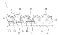
図2は、液晶表示装置1の一部を拡大して示す平面図であり、図1は、図2におけるI−I線断面を示している。
【0046】
液晶表示装置1は、スイッチング素子であるTFT3がマトリクス状に設けられた第1基板2と、該第1基板2上に積層された液晶層(図示省略)と、該液晶層上に積層された第2基板(図示省略)とを備えている。つまり、上記液晶層は、対向する一対の基板間に介装されている。また、上記第2基板は、カラー表示用のRGBのカラーフィルタ(図示省略)や、ITO等により形成された透明電極(図示省略)等を有している。
【0047】
上記第1基板2は、図1に示すように、透明な絶縁性の基板であるガラス基板21と、該ガラス基板21上に上記TFT3を覆って積層された層間絶縁膜12と、該層間絶縁膜12上に積層された反射画素電極11とを備えている。図2に示すように、第1基板2には、平行に延びる複数のソース配線14と、該ソース配線14に垂直に延びる複数のゲート配線10とが設けられている。これらのソース配線14とゲート配線10とにより区画された領域には、複数の画素5が形成されている。上記TFT3及び反射画素電極11は、各画素5毎にそれぞれ設けられている。
【0048】
上記TFT3は、各画素5の隅部に設けられ、信号電圧が供給されるソース電極16と、反射画素電極11に信号電圧を供給するためのドレイン電極15と、上記ソース電極16からドレイン電極15への通電状態を切り換えるためのゲート電極20とを備えている。
【0049】
上記ゲート電極20は、各画素毎にガラス基板21上にパターン形成されている。また、ガラス基板21上には、ゲート電極20を覆うゲート絶縁膜19が積層されている。さらに、ゲート絶縁膜19上には、半導体層18が、ゲート電極20に対応して重なるように設けられている。半導体層18は、例えばアモルファスシリコン(a−Si)等により構成されている。この半導体層18上の略中央部には、チャネル保護層17が設けられている。
【0050】
上記ソース電極16は、チャネル保護層17の一端部と、半導体層18の一部を覆うn+Si層に形成されている。一方、上記ゲート電極19は、チャネル保護層17の他端部と、半導体層18の一部を覆うn+Si層に形成されている。
【0051】
図1及び図2に示すように、ソース電極16には、上記ソース配線14が接続される一方、ドレイン電極15には、ドレイン配線13が接続されている。ドレイン配線13の先端は、ドレイン電極15から反射画素電極11の略中央へ延びている。また、ゲート電極20には、上記ゲート配線10が接続されている。
【0052】
上記層間絶縁膜12は、感光性を有しており、その表面が露光して形成されたなだらかな凹凸面に形成されている。層間絶縁膜12には、画素5の略中方部において積層方向に延びるコンタクトホール30が形成されている。コンタクトホール30は、層間絶縁膜12を貫通しており、該コンタクトホール30下端位置には、上記ドレイン配線13の先端部が配置されている。
【0053】
上記反射画素電極11は、層間絶縁膜12の凹凸面を被覆して設けられ、該層間絶縁膜の凹凸面に沿って形成された凹凸状の反射面を有している。つまり、反射画素電極11の反射面の凹凸は、層間絶縁膜12の凹凸に対応して形成されている。さらに、反射画素電極11は、コンタクトホール30の内周面と、該コンタクトホール30の下側のドレイン配線13とを被覆している。すなわち、反射画素電極11は、コンタクトホール30の底部において、ドレイン配線13を介してTFT3に導通している。
【0054】
そして、本発明の特徴として、上記層間絶縁膜12は、透明性の高い例えばアクリル系感光樹脂などの有機薄膜により構成されると共に、所定の条件で透明状態から発色状態に不可逆的に変化する発色材料を含有している。発色材料は、ワンダイブラック等の示温顔料により構成され、層間絶縁膜12中に均一に分散されている。そして、発色材料は、層間絶縁膜12の凹凸面を形成するための露光後に、発色するように構成されている。本実施形態では、発色材料は、所定温度(例えば、約120〜180℃)以上に加熱されることにより発色し、その発色時に黒色を呈するようになっている。
【0055】
−液晶表示装置の製造方法−
次に、液晶表示装置1の製造方法について、図3を参照して説明する。尚、説明のため、TFT3等の図示は省略し、ドレイン配線13の近傍領域における製造工程を示す。
【0056】
本実施形態に係る液晶表示装置1の製造方法は、第1基板2の製造方法に特徴があり、第1積層工程と、露光工程と、現像工程と、加熱工程と、発色工程と、第2積層工程とを備えている。そして、上記発色工程は、露光工程よりも後に行う。
【0057】
まず、第1積層工程では、図3(a)に示すように、TFT(図示省略)やドレイン配線13が予め設けられたガラス基板21上に、層間絶縁膜12を構成するポジ型の感光性樹脂12を塗布して積層する。
【0058】
次に、露光工程では、図3(b)に示すように、上記第1積層工程で形成された層間絶縁膜12に対し、第1のフォトマスク25を用いて比較的低照度で部分的に露光を行う。第1のフォトマスク25は、図5に示すように、光を透過させる透過部24と、光を遮断する多数の円形状の遮光部23とを有している。すなわち、層間絶縁膜12は、透過部24を透過する光によって部分的に比較的弱く露光される。
【0059】
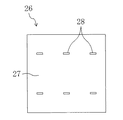
その後、図3(c)に示すように、上記層間絶縁膜112に対し、第2のフォトマスク26を用いて比較的高照度で部分的に露光を行う。第2のフォトマスク26は、図6に示すように、光を透過する透過部28が複数開口され、該透過部28以外の部分が遮光部27に形成されている。そして、透過部28は、上記層間絶縁膜112の露光時に、ドレイン配線113上の所定の位置に対応して配設される。
【0060】
続いて、現像工程では、図3(d)に示すように、上記露光工程で露光された層間絶縁膜12に対し、現像を行うことにより複数の凹部を形成する。すなわち、高照度で露光された部分の感光性樹脂12は、完全に除去されて、コンタクトホール30が形成される。一方、低照度で露光された部分の感光性樹脂12は、所定の深さだけ除去されて、複数の浅い凹部31が形成される。尚、未露光部分の感光性樹脂12も現像により僅かに除去される。
【0061】
次に、加熱工程と発色工程とを行う。加熱工程では、図3(e)に示すように、上記現像工程で形成された各凹部31を約200℃に加熱する。このことにより、層間絶縁膜12の表面を熱だれ現象により変形させ、該層間絶縁膜12上になだらかな凹凸面を形成する。そして、発色工程は、この加熱工程において行う。すなわち、発色工程では、加熱工程における層間絶縁膜12の加熱により、発色材料を黒色に発色させる。
【0062】
その後、第2積層工程では、図3(f)に示すように、上記加熱工程で形成された層間絶縁膜12の凹凸面上に導体膜11を積層することにより、凹凸状の反射面を有する反射画素電極11を形成する。このとき、コンタクトホール30の内周面と、ドレイン配線13とは、反射画素電極11によって覆われる。
【0063】
そして、このように製造された第1基板2に対して、液晶層(図示省略)及び第2基板(図示省略)を積層し、液晶表示装置を製造する。
【0064】
−実施形態1の効果−
以上説明したように、この実施形態1によると、層間絶縁膜12に含まれている発色材料は、層間絶縁膜12の露光前には透明な状態になっている。すなわち、露光工程時に層間絶縁膜12に照射された光を、その強度を維持した状態で、層間絶縁膜12の表面から底部へ向かって入射させることができるため、該層間絶縁膜12を充分に露光することができる。
【0065】
したがって、加熱工程において、層間絶縁膜12に所望の凹凸面を高精度に形成することができ、該層間絶縁膜12の凹凸面上に、反射画素電極11の凹凸状の反射面を精度よく形成することができる。その結果、反射画素電極11の反射面に対して、正反射成分の少ない反射特性を実現し、表示明るさを増大させることができる。
【0066】
そのことに加え、露光工程における層間絶縁膜12の露光後に、発色材料を黒色に発色させるようにしたので、黒色の層間絶縁膜12が露光の障害とならないようにすることができる。そして、この黒色の層間絶縁膜12によって、TFT3への外光を遮蔽することができるため、第2基板(図示省略)にブラックマトリクス等の遮光膜を不要として開口率を大きくすることが可能となる。
【0067】
その結果、反射画素電極11の反射特性を向上させると共に、画素5の開口率を向上させることができるため、液晶表示装置1の表示明るさを一段と増大させることができる。
【0068】
さらに、発色材料を、加熱工程における層間絶縁膜の加熱を利用して発色させるようにしたので、層間絶縁膜を着色するための工程を別途追加する必要がなく、液晶表示装置を容易に製造することができる。
【0069】
また、層間絶縁膜12が黒色に着色されているため、反射画素電極11の膜厚が薄くても、該層間絶縁膜12を介して第1基板2の背面側が透けて見えないようにすることができる。すなわち、表示画質の向上を図ることができる。
【0070】
(実施形態2)
図4は、本発明に係る液晶表示装置の実施形態2を示している。尚、この実施形態において、図1〜図3、図5及び図6と同じ部分については、同じ符号を付してその詳細な説明は省略する。
【0071】
この実施形態2では、層間絶縁膜12に含まれている発色材料は、該層間絶縁膜12を露光する光と同等の所定の波長の光が照射されることにより発色するように構成されている。この発色材料には、例えば、ポリシラン及びロイコ染料等を含有する感光性発色組成物が適用される。
【0072】
すなわち、露光工程で層間絶縁膜12を露光する際に照射される光の波長、及び、発色材料が発色する光の波長は、例えば、300〜450nmの波長を有する紫外光である。
【0073】
−液晶表示装置の製造方法−
次に、液晶表示装置1の製造方法について、図3及び図4を参照して説明する。この実施形態2では、発色工程は、露光工程において行うと共に、加熱工程の後にも行う。
【0074】
第1積層工程については、図3(a)に示すように、上記実施形態1と同様に行われる。その後、図3(b)及び図3(c)に示すように、露光工程では、フォトマスク25,26を介して露光を行う。このとき、発色工程が露光工程中に行われ、層間絶縁膜12の発色材料は、露光時の光により部分的に発色する。
【0075】
続いて、上記実施形態1と同様に、現像工程を行った後に、図4(a)に示す加熱工程が行われる。加熱工程では、現像工程で形成された各凹部31を約200℃に加熱し、層間絶縁膜12の表面になだらかな凹凸面を形成する。
【0076】
その後、さらに発色工程を行い、図4(b)に示すように、上記加熱工程で凹凸面が形成された層間絶縁膜12の全体に対し、上記露光時の光と同等の所定の波長の光を一様に照射することにより、発色材料を黒色に発色させる。
【0077】
続いて、第2積層工程では、図4(c)に示すように、着色された層間絶縁膜12の凹凸面上に、反射画素電極11を積層する。このことにより、層間絶縁膜12の凹凸に対応する凹凸を有する反射面を形成する。
【0078】
−実施形態2の効果−
したがって、この実施形態2によると、露光前に透明な層間絶縁膜12に対し、露光工程中の発色工程から露光工程後の発色工程にかけて、段階的に黒色に着色するようにしたので、上記実施形態1と同様に、反射画素電極11の凹凸状の反射面を精度よく形成して反射特性を向上させると共に、ブラックマトリックスを不要として画素5の開口率を向上させることができるため、液晶表示装置1の表示明るさを増大させることができる。
【0079】
尚、上記実施形態2では、発色工程を、露光工程と、加熱工程の後との双方において行うようにしたが、本発明は、これに限定されるものではない。すなわち、発色工程を露光工程中においてのみ行うようにし、該発色工程における発色材料の発色によって層間絶縁膜12の着色を完了させるようにしてもよい。このことにより、工程数を低減して製造コストを低下させることが可能となる。
【0080】
また、上記各実施形態では、発色材料を、黒色に発色するように構成したが、その他に、例えば灰色等の透明以外の色に発色するように構成してもよい。ただし、遮光の観点から、黒色に発色することが望ましい。
【0081】
【発明の効果】
以上説明したように、本発明によると、層間絶縁膜に予め含有させた透明な発色材料を、層間絶縁膜の露光中又は露光後に発色させることにより、反射画素電極の凹凸面を高精度に形成して反射特性を向上できると共に、ブラックマトリクスを不要として開口率を向上させることができる。その結果、表示明るさをより一段と増大させることができる。
【図面の簡単な説明】
【図1】実施形態1の第1基板を拡大して示す断面図である。
【図2】第1基板を拡大して示す平面図である。
【図3】(a)は、第1積層工程を示す断面図であり、(b)及び(c)は、露光工程を示す断面図であり、(d)は、現像工程を示す断面図であり、(e)は、加熱工程及び発色工程を示す断面図であり、(f)は、第2積層工程を示す断面図である。
【図4】(a)は、加熱工程を示す断面図であり、(b)は、発色工程を示す断面図であり、(c)は、第2積層工程を示す断面図である。
【図5】第1のフォトマスクを示す平面図である。
【図6】第2のフォトマスクを示す平面図である。
【図7】従来の第1基板を示す断面図である。
【図8】(a)は、第1積層工程を示す断面図であり、(b)及び(c)は、露光工程を示す断面図であり、(d)は、現像工程を示す断面図であり、(e)は、加熱工程を示す断面図であり、(f)は、第2積層工程を示す断面図である。
【符号の説明】
1 液晶表示装置
3 TFT(スイッチング素子)
11 反射画素電極
12 層間絶縁膜
21 ガラス基板(基板)[0001]
TECHNICAL FIELD OF THE INVENTION
The present invention relates to a liquid crystal display device for displaying by reflecting incident light and a method for manufacturing the same, and particularly to a measure for increasing display brightness.
[0002]
[Prior art]
2. Description of the Related Art Conventionally, a liquid crystal display device has been suitably used as a display device of a portable device or the like because it can be easily miniaturized. Since mobile devices are usually driven by batteries, it is strongly desired to reduce the power consumption of their display devices. Therefore, a reflection type liquid crystal display device that does not require a light source such as a backlight and consumes less power has attracted attention.
[0003]
The reflection type liquid crystal display device is configured to reflect natural light incident from the outside toward the observer to perform display. Therefore, in order to obtain a bright display, it is necessary to increase the intensity of light scattered in a direction perpendicular to the display screen with respect to incident light from a wide angle. Therefore, it has been conventionally known to form a surface of a reflective pixel electrode that reflects incident light on an uneven surface in a reflective liquid crystal display device (for example, see Patent Document 1).
[0004]
FIG. 7 shows an enlarged part of a conventional reflection type liquid crystal display device. The reflective liquid
[0005]
As shown in FIG. 7, the
[0006]
In the interlayer
[0007]
In this manner, in addition to providing the interlayer
[0008]
Next, a method of manufacturing the
[0009]
First, as shown in FIG. 8A, a positive
[0010]
Next, as shown in FIG. 8B, the
[0011]
Thereafter, as shown in FIG. 8C, the
[0012]
Subsequently, as shown in FIG. 8D, by developing the
[0013]
Next, as shown in FIG. 8E, by performing a heat treatment at about 200 ° C., the surface of the
[0014]
Thereafter, on the surface of the interlayer
[0015]
By the way, the reflection type liquid
[0016]
Therefore, conventionally, instead of providing a black matrix, it is known that a black pigment or the like is dispersed and contained in an interlayer insulating film in advance and colored (for example, see Patent Document 2). That is, by providing a light-shielding property to the interlayer insulating film itself, a black matrix is not required, deterioration of TFT characteristics is prevented, and an aperture ratio is improved as much as possible.
[0017]
[Patent Document 1]
JP 2000-258762 A
[Patent Document 2]
JP-A-10-161144
[0018]
[Problems to be solved by the invention]
Therefore, in contrast to the reflection type liquid crystal display device having a reflective pixel electrode having a gently uneven reflection surface as in Patent Document 1, in order to further increase the display brightness, an interlayer as in
[0019]
However, in actuality, if the interlayer insulating film is black, it is difficult to sufficiently expose the interlayer insulating film, so that the amount of exposure is controlled to form an uneven surface or a contact hole in the interlayer insulating film with high precision. It is difficult to do. As a result, there is a problem that it is difficult to form a reflection surface having a smooth uneven surface with high precision on the reflection pixel electrode and to realize a desired reflection characteristic with a small regular reflection component.
[0020]
The present invention has been made in view of the above points, and an object of the present invention is to provide a liquid crystal display device and a method of manufacturing the same, in which a concave and convex surface of a reflective pixel electrode is formed with high precision to improve reflection characteristics. Another object of the present invention is to increase the display brightness as much as possible by improving the aperture ratio without using a black matrix.
[0021]
[Means for Solving the Problems]
In order to achieve the above object, in the present invention, a transparent coloring material is previously contained in the interlayer insulating film, and the coloring material is colored during or after the exposure of the interlayer insulating film.
[0022]
Specifically, the invention according to claim 1 is directed to a liquid crystal display device that performs display by reflecting light incident through a liquid crystal layer. And an insulating substrate provided with the switching element, an interlayer insulating film having a concave-convex surface formed by exposure, laminated on the substrate to cover the switching element, and laminated on the interlayer insulating film, A reflective pixel electrode having an uneven reflecting surface formed along the uneven surface of the interlayer insulating film, and a reflective pixel electrode electrically connected to the switching element, wherein the interlayer insulating film develops a color from a transparent state under predetermined conditions. Contains a coloring material that changes to a state.
[0023]
According to the above invention, the coloring material contained in the interlayer insulating film is in a transparent state before a predetermined condition is given. That is, the light applied to the interlayer insulating film at the time of exposure is easily incident from the surface of the interlayer insulating film toward the bottom while maintaining the intensity, so that the interlayer insulating film can be sufficiently exposed. It becomes.
[0024]
As a result, a desired uneven surface can be formed on the interlayer insulating film with high accuracy, and thus the uneven reflecting surface of the reflective pixel electrode can be formed accurately on the uneven surface of the interlayer insulating film. That is, since the reflection characteristics with less regular reflection components can be realized on the reflection surface of the reflection pixel electrode, the display brightness increases.
[0025]
Further, by applying a predetermined condition during or after the exposure of the interlayer insulating film to develop the color-forming material, the formation of the uneven surface of the interlayer insulating film and the reflective pixel electrode does not hinder the formation of the interlayer insulating film. Can be colored. The colored interlayer insulating film suppresses external light from entering the switch element. As a result, the display brightness can be further increased by increasing the aperture ratio without using the black matrix.
[0026]
The invention according to
[0027]
According to the present invention, the coloring material is colored by heating the interlayer insulating film to a predetermined temperature or higher, and the interlayer insulating film is colored.
[0028]
According to a third aspect of the present invention, in the first aspect of the present invention, the color-forming material is colored by being irradiated with light having a predetermined wavelength.
[0029]
According to the present invention, by irradiating the interlayer insulating film with the light having the predetermined wavelength, the coloring material is colored, and the interlayer insulating film is colored.
[0030]
According to a fourth aspect of the present invention, in the first aspect of the present invention, the color-forming material exhibits black color at the time of coloring.
[0031]
According to the present invention, external light incident on the interlayer insulating film is effectively blocked by the black interlayer insulating film.
[0032]
The invention according to
[0033]
According to the above invention, the interlayer insulating film laminated on the substrate in the first laminating step is partially exposed in the next exposing step. At the time of this exposure, since the coloring material of the interlayer insulating film is in a transparent state, the light applied to the interlayer insulating film at the time of exposure enters the surface of the interlayer insulating film from the surface to the bottom while maintaining the intensity. That is, the interlayer insulating film is sufficiently exposed.
[0034]
Thereafter, in the interlayer insulating film, after a plurality of concave portions are formed in the developing step, a gentle uneven surface is formed in the heating step. After that, on the uneven surface of the interlayer insulating film, a reflective pixel electrode having an uneven reflective surface is formed in the second laminating step.
[0035]
Then, during or after the exposing step, a coloring step is performed, whereby the coloring material is colored, and the interlayer insulating film is colored. That is, the color forming step may be performed during or after the exposure step, may be performed during or after the developing step, and may be performed during or after the heating step.
[0036]
As a result, the uneven reflection surface of the reflection pixel electrode can be formed with high precision, the reflection characteristics with less regular reflection component can be realized, and the aperture ratio is improved by eliminating the need for the black matrix by the colored interlayer insulating film. Brightness can be further increased.
[0037]
According to a sixth aspect of the present invention, in the fifth aspect of the invention, the coloring material is colored by being heated to a predetermined temperature or higher, and the coloring step is performed in a heating step. The color forming material is colored by heating the interlayer insulating film in the step (1).
[0038]
According to the present invention, the coloring material is colored by utilizing the heating of the interlayer insulating film in the heating step. That is, the interlayer insulating film is colored simultaneously with the formation of the gentle uneven surface in the heating step (coloring step). Therefore, it is not necessary to separately add a step for coloring the interlayer insulating film, so that the interlayer insulating film can be easily manufactured.
[0039]
In the invention according to claim 7, in the invention according to
[0040]
According to the above invention, the interlayer insulating film is colored by irradiating the coloring material with light having the same wavelength as the light at the time of exposure in the coloring step.
[0041]
According to an eighth aspect of the present invention, in the fifth aspect of the invention, the color-forming material develops black in a color-forming step.
[0042]
According to the present invention, external light incident on the interlayer insulating film is effectively blocked by the interlayer insulating film colored black in the coloring step.
[0043]
BEST MODE FOR CARRYING OUT THE INVENTION
Hereinafter, embodiments of the present invention will be described in detail with reference to the drawings.
[0044]
(Embodiment 1)
1 to 3 show a first embodiment of a liquid crystal display device according to the present invention. The liquid crystal display device 1 is a reflection type liquid crystal display device that performs display by reflecting external light incident through a liquid crystal layer (not shown).
[0045]
FIG. 2 is an enlarged plan view showing a part of the liquid crystal display device 1, and FIG. 1 is a cross-sectional view taken along line II in FIG.
[0046]
The liquid crystal display device 1 includes a
[0047]
As shown in FIG. 1, the
[0048]
The
[0049]
The
[0050]
The source electrode 16 covers one end of the
[0051]
As shown in FIGS. 1 and 2, the
[0052]
The
[0053]
The
[0054]
As a feature of the present invention, the
[0055]
-Manufacturing method of liquid crystal display device-
Next, a method for manufacturing the liquid crystal display device 1 will be described with reference to FIG. For the sake of explanation, illustration of the
[0056]
The method for manufacturing the liquid crystal display device 1 according to the present embodiment is characterized by the method for manufacturing the
[0057]
First, in the first laminating step, as shown in FIG. 3A, a positive type photosensitive film forming the
[0058]
Next, in the exposing step, as shown in FIG. 3B, the
[0059]
Thereafter, as shown in FIG. 3C, the
[0060]
Subsequently, in a developing step, as shown in FIG. 3D, a plurality of recesses are formed by performing development on the
[0061]
Next, a heating step and a coloring step are performed. In the heating step, as shown in FIG. 3E, each
[0062]
Then, in the second laminating step, as shown in FIG. 3 (f), the
[0063]
Then, a liquid crystal layer (not shown) and a second substrate (not shown) are laminated on the
[0064]
-Effects of Embodiment 1-
As described above, according to the first embodiment, the coloring material contained in the
[0065]
Therefore, in the heating step, a desired uneven surface can be formed on the
[0066]
In addition, since the coloring material is colored black after the exposure of the
[0067]
As a result, the reflection characteristics of the
[0068]
Further, since the coloring material is colored by utilizing the heating of the interlayer insulating film in the heating step, there is no need to add a separate step for coloring the interlayer insulating film, and the liquid crystal display device can be easily manufactured. be able to.
[0069]
In addition, since the
[0070]
(Embodiment 2)
FIG. 4 shows a second embodiment of the liquid crystal display device according to the present invention. In this embodiment, the same portions as those in FIGS. 1 to 3, 5 and 6 are denoted by the same reference numerals, and detailed description thereof will be omitted.
[0071]
In the second embodiment, the coloring material included in the
[0072]
That is, the wavelength of light emitted when exposing the
[0073]
-Manufacturing method of liquid crystal display device-
Next, a method for manufacturing the liquid crystal display device 1 will be described with reference to FIGS. In the second embodiment, the coloring step is performed in the exposure step and also after the heating step.
[0074]
The first laminating step is performed in the same manner as in the first embodiment, as shown in FIG. Thereafter, as shown in FIGS. 3B and 3C, in the exposure step, exposure is performed via
[0075]
Subsequently, as in the first embodiment, after performing the developing process, the heating process illustrated in FIG. 4A is performed. In the heating step, each
[0076]
Thereafter, a color developing step is further performed, and as shown in FIG. 4B, light of a predetermined wavelength equivalent to the light at the time of the exposure is applied to the entire
[0077]
Subsequently, in the second laminating step, as shown in FIG. 4C, the
[0078]
-Effect of Embodiment 2-
Therefore, according to the second embodiment, the transparent
[0079]
In the second embodiment, the color forming step is performed both in the exposing step and after the heating step. However, the present invention is not limited to this. That is, the coloring step may be performed only during the exposure step, and the coloring of the
[0080]
Further, in each of the above embodiments, the color-forming material is configured to emit black, but may be configured to emit a color other than transparent, such as gray, for example. However, from the viewpoint of light shielding, it is desirable to develop a black color.
[0081]
【The invention's effect】
As described above, according to the present invention, a transparent coloring material previously contained in the interlayer insulating film is colored during or after exposure of the interlayer insulating film, thereby forming the uneven surface of the reflective pixel electrode with high precision. As a result, the reflection characteristics can be improved, and the aperture ratio can be improved by eliminating the need for the black matrix. As a result, the display brightness can be further increased.
[Brief description of the drawings]
FIG. 1 is an enlarged cross-sectional view illustrating a first substrate according to a first embodiment.
FIG. 2 is an enlarged plan view showing a first substrate.
3A is a cross-sectional view illustrating a first laminating step, FIGS. 3B and 3C are cross-sectional views illustrating an exposing step, and FIG. 3D is a cross-sectional view illustrating a developing step. FIG. 4E is a cross-sectional view illustrating a heating step and a color forming step, and FIG. 4F is a cross-sectional view illustrating a second laminating step.
4A is a sectional view showing a heating step, FIG. 4B is a sectional view showing a coloring step, and FIG. 4C is a sectional view showing a second laminating step.
FIG. 5 is a plan view showing a first photomask.
FIG. 6 is a plan view showing a second photomask.
FIG. 7 is a cross-sectional view showing a conventional first substrate.
8A is a cross-sectional view illustrating a first laminating step, FIGS. 8B and 8C are cross-sectional views illustrating an exposing step, and FIG. 8D is a cross-sectional view illustrating a developing step. FIG. 4E is a cross-sectional view illustrating a heating step, and FIG. 4F is a cross-sectional view illustrating a second laminating step.
[Explanation of symbols]
1 Liquid crystal display device
3 TFT (switching element)
11 Reflection pixel electrode
12 interlayer insulating film
21 Glass substrate (substrate)
Claims (8)
スイッチング素子が設けられた絶縁性の基板と、
上記基板上にスイッチング素子を覆って積層され、露光して形成された凹凸面を有する層間絶縁膜と、
上記層間絶縁膜上に積層され、該層間絶縁膜の凹凸面に沿って形成された凹凸状の反射面を有すると共に、上記スイッチング素子に導通された反射画素電極とを備え、
上記層間絶縁膜は、所定の条件で透明状態から発色状態に変化する発色材料を含有している
ことを特徴とする液晶表示装置。A liquid crystal display device that performs display by reflecting light incident through a liquid crystal layer,
An insulating substrate provided with a switching element;
An interlayer insulating film having a concave-convex surface formed by exposing, laminated on the substrate, covering the switching element,
A reflective pixel electrode that is stacked on the interlayer insulating film and has an uneven reflective surface formed along the uneven surface of the interlayer insulating film, and a reflective pixel electrode that is electrically connected to the switching element;
The liquid crystal display device, wherein the interlayer insulating film contains a coloring material that changes from a transparent state to a colored state under a predetermined condition.
上記発色材料は、所定温度以上に加熱されることにより発色する
ことを特徴とする液晶表示装置。In claim 1,
A liquid crystal display device, wherein the coloring material develops a color when heated to a predetermined temperature or higher.
上記発色材料は、所定の波長の光が照射されることにより発色する
ことを特徴とする液晶表示装置。In claim 1,
A liquid crystal display device, wherein the coloring material is colored when irradiated with light of a predetermined wavelength.
上記発色材料は、発色時に黒色を呈する
ことを特徴とする液晶表示装置。In claim 1,
The liquid crystal display device, wherein the coloring material exhibits black color when coloring.
スイッチング素子が設けられた絶縁性の基板上に、感光性を有する層間絶縁膜を積層する第1積層工程と、
上記第1積層工程で形成された層間絶縁膜に対し、部分的に露光を行う露光工程と、
上記露光工程で露光された層間絶縁膜に対し、現像を行うことにより複数の凹部を形成する現像工程と、
上記現像工程で形成された各凹部を加熱することにより、該層間絶縁膜上になだらかな凹凸面を形成する加熱工程と、
上記加熱工程で形成された層間絶縁膜の凹凸面上に導体膜を積層することにより、凹凸状の反射面を有する反射画素電極を形成する第2積層工程とを備え、
上記第1積層工程で基板上に積層される層間絶縁膜には、所定の条件で透明状態から発色状態に変化する発色材料が含有されており、
上記露光工程中又は露光工程後に、上記発色材料を発色させる発色工程を備えている
ことを特徴とする液晶表示装置の製造方法。A method for manufacturing a liquid crystal display device that performs display by reflecting light incident through a liquid crystal layer,
A first laminating step of laminating a photosensitive interlayer insulating film on an insulating substrate provided with a switching element;
An exposure step of partially exposing the interlayer insulating film formed in the first laminating step;
A developing step of forming a plurality of recesses by performing development on the interlayer insulating film exposed in the exposure step;
By heating each concave portion formed in the developing step, a heating step of forming a smooth uneven surface on the interlayer insulating film,
A second laminating step of forming a reflective pixel electrode having a concave-convex reflective surface by laminating a conductive film on the concave-convex surface of the interlayer insulating film formed in the heating step,
The interlayer insulating film laminated on the substrate in the first laminating step contains a coloring material that changes from a transparent state to a colored state under predetermined conditions,
A method for producing a liquid crystal display device, comprising a color forming step of coloring the color forming material during or after the exposure step.
上記発色材料は、所定温度以上に加熱されることにより発色するものであり、
発色工程は、加熱工程において行われ、該加熱工程における層間絶縁膜の加熱により上記発色材料を発色させる
ことを特徴とする液晶表示装置の製造方法。In claim 5,
The coloring material is one that develops color when heated to a predetermined temperature or higher,
The method for producing a liquid crystal display device, wherein the coloring step is performed in a heating step, and the coloring material is colored by heating the interlayer insulating film in the heating step.
上記発色材料は、所定の波長の光が照射されることにより発色するものであり、
発色工程では、露光時の光と同等の波長の光を照射することにより上記発色材料を発色させる
ことを特徴とする液晶表示装置の製造方法。In claim 5,
The coloring material is a material that develops color when irradiated with light of a predetermined wavelength,
In the color forming step, a method for manufacturing a liquid crystal display device, characterized in that the color forming material is colored by irradiating light having the same wavelength as light at the time of exposure.
上記発色材料は、発色工程において黒色に発色する
ことを特徴とする液晶表示装置の製造方法。In claim 5,
The method for manufacturing a liquid crystal display device, wherein the coloring material develops a black color in a coloring step.
Priority Applications (1)
| Application Number | Priority Date | Filing Date | Title |
|---|---|---|---|
| JP2003041368A JP2004252071A (en) | 2003-02-19 | 2003-02-19 | Liquid crystal display and method for manufacturing the same |
Applications Claiming Priority (1)
| Application Number | Priority Date | Filing Date | Title |
|---|---|---|---|
| JP2003041368A JP2004252071A (en) | 2003-02-19 | 2003-02-19 | Liquid crystal display and method for manufacturing the same |
Publications (1)
| Publication Number | Publication Date |
|---|---|
| JP2004252071A true JP2004252071A (en) | 2004-09-09 |
Family
ID=33024967
Family Applications (1)
| Application Number | Title | Priority Date | Filing Date |
|---|---|---|---|
| JP2003041368A Pending JP2004252071A (en) | 2003-02-19 | 2003-02-19 | Liquid crystal display and method for manufacturing the same |
Country Status (1)
| Country | Link |
|---|---|
| JP (1) | JP2004252071A (en) |
Cited By (5)
| Publication number | Priority date | Publication date | Assignee | Title |
|---|---|---|---|---|
| JP2008158522A (en) * | 2006-12-22 | 2008-07-10 | Samsung Corning Co Ltd | External light shielding film and optical filter for display apparatus having the same |
| US7847904B2 (en) | 2006-06-02 | 2010-12-07 | Semiconductor Energy Laboratory Co., Ltd. | Liquid crystal display device and electronic appliance |
| US8338865B2 (en) | 2006-05-16 | 2012-12-25 | Semiconductor Energy Laboratory Co., Ltd. | Liquid crystal display device and semiconductor device |
| US8687157B2 (en) | 2005-10-18 | 2014-04-01 | Semiconductor Energy Laboratory Co., Ltd. | Liquid crystal display device |
| US9207504B2 (en) | 2006-04-06 | 2015-12-08 | Semiconductor Energy Laboratory Co., Ltd. | Liquid crystal display device, semiconductor device, and electronic appliance |
-
2003
- 2003-02-19 JP JP2003041368A patent/JP2004252071A/en active Pending
Cited By (24)
| Publication number | Priority date | Publication date | Assignee | Title |
|---|---|---|---|---|
| US8687157B2 (en) | 2005-10-18 | 2014-04-01 | Semiconductor Energy Laboratory Co., Ltd. | Liquid crystal display device |
| US9958736B2 (en) | 2006-04-06 | 2018-05-01 | Semiconductor Energy Laboratory Co., Ltd. | Liquid crystal display device, semiconductor device, and electronic appliance |
| US11921382B2 (en) | 2006-04-06 | 2024-03-05 | Semiconductor Energy Laboratory Co., Ltd. | Liquid crystal display device, semiconductor device, and electronic appliance |
| US11644720B2 (en) | 2006-04-06 | 2023-05-09 | Semiconductor Energy Laboratory Co., Ltd. | Liquid crystal display device, semiconductor device, and electronic appliance |
| US11442317B2 (en) | 2006-04-06 | 2022-09-13 | Semiconductor Energy Laboratory Co., Ltd. | Liquid crystal display device, semiconductor device, and electronic appliance |
| US11073729B2 (en) | 2006-04-06 | 2021-07-27 | Semiconductor Energy Laboratory Co., Ltd. | Liquid crystal display device, semiconductor device, and electronic appliance |
| US9207504B2 (en) | 2006-04-06 | 2015-12-08 | Semiconductor Energy Laboratory Co., Ltd. | Liquid crystal display device, semiconductor device, and electronic appliance |
| US9213206B2 (en) | 2006-04-06 | 2015-12-15 | Semiconductor Energy Laboratory Co., Ltd. | Liquid crystal display device, semiconductor device, and electronic appliance |
| US10684517B2 (en) | 2006-04-06 | 2020-06-16 | Semiconductor Energy Laboratory Co., Ltd. | Liquid crystal display device, semiconductor device, and electronic appliance |
| US11435626B2 (en) | 2006-05-16 | 2022-09-06 | Semiconductor Energy Laboratory Co., Ltd. | Liquid crystal display device and semiconductor device |
| US8872182B2 (en) | 2006-05-16 | 2014-10-28 | Semiconductor Energy Laboratory Co., Ltd. | Liquid crystal display device and semiconductor device |
| US10001678B2 (en) | 2006-05-16 | 2018-06-19 | Semiconductor Energy Laboratory Co., Ltd. | Liquid crystal display device and semiconductor device |
| US11726371B2 (en) | 2006-05-16 | 2023-08-15 | Semiconductor Energy Laboratory Co., Ltd. | FFS-mode liquid crystal display device comprising a top-gate transistor and an auxiliary wiring connected to a common electrode in a pixel portion |
| US10509271B2 (en) | 2006-05-16 | 2019-12-17 | Semiconductor Energy Laboratory Co., Ltd. | Liquid crystal display device comprising a semiconductor film having a channel formation region overlapping with a conductive film in a floating state |
| US9268188B2 (en) | 2006-05-16 | 2016-02-23 | Semiconductor Energy Laboratory Co., Ltd. | Liquid crystal display device and semiconductor device |
| US11061285B2 (en) | 2006-05-16 | 2021-07-13 | Semiconductor Energy Laboratory Co., Ltd. | Liquid crystal display device comprising a dogleg-like shaped pixel electrode in a plane view having a plurality of dogleg-like shaped openings and semiconductor device |
| US9709861B2 (en) | 2006-05-16 | 2017-07-18 | Semiconductor Energy Laboratory Co., Ltd. | Liquid crystal display device and semiconductor device |
| US11106096B2 (en) | 2006-05-16 | 2021-08-31 | Semiconductor Energy Laboratory Co., Ltd. | Liquid crystal display device and semiconductor device |
| US8338865B2 (en) | 2006-05-16 | 2012-12-25 | Semiconductor Energy Laboratory Co., Ltd. | Liquid crystal display device and semiconductor device |
| US8841671B2 (en) | 2006-05-16 | 2014-09-23 | Semiconductor Energy Laboratory Co., Ltd. | Liquid crystal display device and semiconductor device |
| US10095070B2 (en) | 2006-06-02 | 2018-10-09 | Semiconductor Energy Laboratory Co., Ltd. | Liquid crystal display device and electronic appliance |
| US7847904B2 (en) | 2006-06-02 | 2010-12-07 | Semiconductor Energy Laboratory Co., Ltd. | Liquid crystal display device and electronic appliance |
| US11960174B2 (en) | 2006-06-02 | 2024-04-16 | Semiconductor Energy Laboratory Co., Ltd. | Liquid crystal display device and electronic appliance |
| JP2008158522A (en) * | 2006-12-22 | 2008-07-10 | Samsung Corning Co Ltd | External light shielding film and optical filter for display apparatus having the same |
Similar Documents
| Publication | Publication Date | Title |
|---|---|---|
| US7310126B2 (en) | Reflective LCD comprising reflective surface including convex portions whose elevation varying cycles is greater than pitch of convex portions | |
| US6665030B2 (en) | Liquid crystal display device with projection-recess patterns formed in pixel regions for reflecting incident light | |
| US7875477B2 (en) | Manufacturing method of liquid crystal display | |
| JP4410776B2 (en) | Manufacturing method of liquid crystal display device | |
| JP2006171752A (en) | Transflective liquid crystal display device and manufacturing method thereof | |
| JP2007114770A (en) | Array substrate, method of manufacturing the same and liquid crystal display device having the same | |
| TWI304497B (en) | ||
| US7123327B2 (en) | Substrate for reflective-transmissive electro-optical device having opening in base layer varying in size along a first direction | |
| KR20060018137A (en) | Semi-transmission lcd and method of making the same | |
| JP2004252071A (en) | Liquid crystal display and method for manufacturing the same | |
| JP4107047B2 (en) | Transflective liquid crystal display device | |
| KR101290168B1 (en) | Transflective liquid crystal display device | |
| KR20100059448A (en) | Thin film transistor array panel and manufacturing method thereof | |
| JP4154880B2 (en) | Electro-optical device and manufacturing method thereof | |
| KR20070109289A (en) | Fabrication method of display device | |
| US20070153149A1 (en) | Tft substrate, liquid crystal display panel, and methods for manufacturing the same | |
| KR100736627B1 (en) | A color filter panel for liquid crystal display and manufacturing method thereof | |
| KR20070049719A (en) | Display substrate, method of manufacturing thereof and display apparatus having the same | |
| JP2007128117A (en) | Liquid crystal display device and method for manufacturing the same | |
| KR100995581B1 (en) | Color filter substrate, liquid crystal display apparatus having the same and method for manufacturing the same | |
| KR20080003103A (en) | Transflective liquid crystal display device and fabricating thereof | |
| KR100993831B1 (en) | Upper substrate, liquid crystal display apparatus having the same and method for manufacturing the same | |
| KR101174286B1 (en) | Semi-transparent type liquid crystal display and method for fabricating the same | |
| KR100993819B1 (en) | Liquid crystal display and method of manufacturing the same | |
| JP2003015099A (en) | Optoelectronic device, electronic instrument and method for manufacturing optoelectronic device |