JP4154880B2 - Electro-optical device and manufacturing method thereof - Google Patents
Electro-optical device and manufacturing method thereof Download PDFInfo
- Publication number
- JP4154880B2 JP4154880B2 JP2001294719A JP2001294719A JP4154880B2 JP 4154880 B2 JP4154880 B2 JP 4154880B2 JP 2001294719 A JP2001294719 A JP 2001294719A JP 2001294719 A JP2001294719 A JP 2001294719A JP 4154880 B2 JP4154880 B2 JP 4154880B2
- Authority
- JP
- Japan
- Prior art keywords
- region
- electro
- optical device
- layer
- forming
- Prior art date
- Legal status (The legal status is an assumption and is not a legal conclusion. Google has not performed a legal analysis and makes no representation as to the accuracy of the status listed.)
- Expired - Fee Related
Links
Images


Description
【0001】
【発明の属する技術分野】
本発明は、電気光学装置及びその製造方法に関する。さらに詳しくは、携帯電話機、モバイルコンピュータ等に好適に用いられる、透過窓の部分にも配向処理が十分に施され、画素内の透過モード表示におけるコントラストに優れるとともに、反射特性にも優れた電気光学装置及びその製造方法に関する。
【0002】
【従来の技術】
電気光学装置(例えば、液晶表示装置、EL発光表示装置等)は、携帯電話機、モバイルコンピュータ等の各種機器の直視型の表示装置として広く用いられている。このような電気光学装置のうち、例えば、アクティブマトリクス型で、半透過・半反射型の液晶表示装置においては、対向配置されたTFTアレイ基板と対向基板とがシール材で貼り合わされているとともに、基板間のシール材で区画された領域内に電気光学物質としての液晶が封入、保持されている。
【0003】
また、TFTアレイ基板の表面に、対向基板の側から入射してきた外光を対向基板の方向に反射するための反射電極が形成されており、対向基板側から入射した光をTFTアレイ基板の反射電極で反射し、対向基板側から出射した光によって画像を表示する(反射モード)。また、反射電極には光を透過する透過窓が形成され、この透過窓を覆うように、反射電極の下層側に透明電極が形成され、バックライトからの光のうち透過窓を透過した光によって画像を表示する(透過モード)。
【0004】
このような液晶表示装置に用いられるTFTアレイ基板120としては、例えば、図14(A)に示すように、画素110の一部に、後述する凹凸層(図示せず)と、この凹凸層上に形成された、外光を反射して画像を表示する反射電極108(反射電極108には、凹凸層の表面凹凸形状に対応した形状の反射用の凹凸109が形成されている)と、反射電極108を形成しない部分である透過窓107と、透過窓107に対応した領域を覆うように形成されたITO(Indium Tin Oxide)からなる透明電極(図示せず)とを備えたものとし、バックライト(図示せず)からの光を、透過窓107から透過させて画像を表示するものが用いられている。このようなTFTアレイ基板120は、図14(B)に示すように(図14(B)は図14(A)のC−C’線における断面図である)、基板101上に、シリコン酸化膜(SiO2膜)等の下地保護膜102、ITO等からなる透明電極103及びアルミニウムもしくはアルミニウムの合金あるいはアルミニウムの積層膜からなるソース線(図示せず)、薄膜トランジスタ(図示せず)、シリコン窒化膜(SiN膜)等の保護膜104(この保護膜104は形成しない場合がある)、反射電極108の表面に反射用の凹凸109を形成するためのアクリル樹脂等の有機系の感光性樹脂の2層からなる凹凸形成層105及び凹凸層106、及びアルミニウムや銀、もしくはこれらの合金、又はチタン、窒化チタン、モリブデン、タンタル等との積層膜からなり、透過窓107を有する反射電極108等を積層して形成されている。
【0005】
【発明が解決しようとする課題】
このような構成の反射電極を用いた液晶表示装置は、外光の明るさに影響されず、視認性に優れた液晶表示装置を提供することを可能にしたが、一方、反射電極108の表面に反射用の凹凸109を形成するために用いられるアクリル樹脂等からなる凹凸形成層105及び凹凸層106の膜厚は、2層で最大5μmにも達するほど大きいため、凹凸形成層105及び凹凸層106が存在しない透過窓107の部分においては、画素全体ではかなり薄い構造(段差を有する構造)になる。このためポリイミド等の配向膜の形成(塗布)時、配向膜は、透過窓107の部分には形成(塗布)されず、また、十分な配向処理を施すことが困難になり、表示特性に悪影響を及ぼすことになる。例えば、ノーマリホワイトの場合、電位を加えても、透過窓107の部分だけ黒くならず、白く見えてしまうという問題があった。
【0006】
本発明は、上述の問題に鑑みてなされたものであって、透過窓の部分にも配向処理が十分に施された、画素内の透過モード表示におけるコントラストに優れるとともに、反射特性にも優れた電気光学装置及びその製造方法を提供することを目的とする。
【0007】
【課題を解決するための手段】
上述の目的を達成するために、本発明の電気光学装置は、複数の画素を含んでなる画像表示領域を有し、各複数の画素が入射光を反射する反射領域、及び入射光を透過する透過領域を含んでなる電気光学装置において、反射領域には反射性を備えた金属膜が形成されてなり、透過領域には透明電極が少なくとも形成されており、反射領域及び透過領域の両領域においては金属膜及び透明電極の上層に配向膜が形成されているとともに、金属膜及び透明電極の下層に金属膜の表面を凹凸形状にする凹凸パターンが形成され、凹凸パターンの凸部分は、透過領域と反射領域との境界部分を跨がないように配設され、透明電極の形成領域は、金属膜の形成領域よりも広いことを特徴とする。
また、金属膜は、透明電極の表面に形成されていることが好ましい。
また、凹凸パターンは、凸部分の基礎となる第1形成層と、第1形成層を覆う第2形成層とからなり、第2形成層は、第1形成層におけるエッジが凹凸パターンに現れないように形成されることが好ましい。
また、複数の画素は、それぞれがスイッチング用のTFTと、画素電極に印加される電圧を保持するための蓄積容量とを有し、TFTおよび蓄積容量は反射領域に形成され、反射領域におけるTFTおよび蓄積容量が形成された領域には、第2形成層のみが積層されていることが好ましい。
【0008】
このように構成することによって、反射電極の表面に、反射光を適度に散乱させる表面凹凸形状(反射用の凹凸)を備え、また、透過窓の部分にも配向膜を十分に形成(塗布)して、配向処理を十分に施すことが可能になり、画素内の透過モード表示におけるコントラストに優れるとともに、反射特性にも優れた電気光学装置を提供することができる。
【0009】
また、本発明の電気光学装置は、前記凹凸層の凸部分が、前記透過窓に対応した領域とそれ以外の領域との境界部分を跨ることなく前記境界部分の内側又は外側のいずれかに位置するように配設されるものであることが好ましい。
【0010】
このように構成することによって、反射電極にフォトリソグラフィ技術及びエッチング技術を用いて透過窓の形成を行う場合、エッチング剤等が、反射電極と凹凸層の間に侵入するのを有効に防ぐことができる。
【0011】
また、本発明の電気光学装置は、前記凹凸層が、透光性の感光性樹脂から形成されてなるものであることが好ましい。
【0012】
このように構成することによって、製造工程を効率化することができるとともに、透過特性の低減を防止することができる。
【0013】
また、本発明の電気光学装置は、前記凹凸層の下層側に、凹凸形成層がさらに配設されてなるものであることが好ましい。
【0014】
このように構成することによって、エッジや、平坦部分の少ない滑らかな表面凹凸形状を有する凹凸層を容易に形成することができる。
【0015】
また、本発明の電気光学装置は、前記凹凸形成層が、透光性の感光性樹脂から形成されてなるものであることが好ましい。
【0016】
このように構成することによって、所望の位置に、所望の大きさの、表面凹凸形状を有する凹凸層を効率よく形成することができる。
【0017】
また、本発明の電気光学装置は、前記反射電極が、アルミニウムや銀、もしくはこれらの合金、又はチタン、窒化チタン、モリブデン、タンタル等との積層膜から構成されたものであることが好ましい。
【0018】
このように構成することによって、光反射効率を高めることができる。
【0019】
また、本発明の電気光学装置は、前記透明電極が、ITO膜から構成されたものであることが好ましい。
【0020】
このように構成することによって、透過モード表示におけるコントラストを高めることができる。
【0021】
また、本発明の電気光学装置は、前記透明電極の形成領域が、前記反射電極の形成領域よりも広いものであることが好ましい。
【0022】
このように構成することによって、透過モード表示におけるコントラストを高めることができる。
【0023】
また、本発明の電気光学装置は、前記透明電極と前記反射電極とが、電気的に接続されてなるものであることが好ましい。
【0024】
このように構成することによって、消費電力の低減化を図ることができる。
【0025】
また、本発明の電気光学装置は、前記透明電極が、前記透過窓の外側で電位供給線と電気的に接続されてなるものであることが好ましい。
【0026】
このように構成することによって、消費電力の低減化を図ることができる。
【0027】
また、本発明の電気光学装置の製造方法は、複数の画素を含んでなる画像表示領域を有し、各複数の画素が入射光を反射する反射領域、及び入射光を透過する透過領域を含んでなる電気光学装置の製造方法において、基板の上層に、第1形成層を形成する工程と、第1形成層におけるエッジが表面に現れないように第1形成層を覆う第2形成層を形成する工程と、第1形成層および第1形成層からなる凹凸パターン上に透明電極を形成する工程と、透明電極の表面に金属膜を形成する工程と、金属膜のエッチングを含み、透明電極を露出させた透過領域を有する反射電極を形成する工程と、反射領域及び透過領域の両領域に配向膜を形成する工程と、を具備してなり、凹凸パターンの凸部分は、透過領域と反射領域との境界部分を跨がないように配設されることを特徴とする。
【0028】
このように構成することによって、反射電極の表面に、反射光を適度に散乱させる表面凹凸形状(反射用の凹凸)を備え、画素内の透過モード表示におけるコントラストに優れるとともに、反射特性にも優れた電気光学装置を効率よくかつ低コストで提供することができる。
【0029】
この場合、前記凹凸層の凸部分を、前記透過窓に対応した領域とそれ以外の領域との境界部分を跨ることなく前記境界部分の内側又は外側のいずれかに位置するように配設することが好ましい。
【0030】
このように構成することによって、反射電極にフォトリソグラフィ技術及びエッチング技術を用いて透過窓の形成を行う場合、エッチング剤等が、反射電極と凹凸層の間に侵入するのを有効に防ぐことができる。
【0031】
また、本発明の電気光学装置の製造方法は、前記凹凸層を、透光性の感光性樹脂から形成することが好ましい。
【0032】
このように構成することによって、製造工程を効率化することができるとともに、透過特性の低減を防止することができる。
【0033】
また、本発明の電気光学装置の製造方法は、前記凹凸層の下層側に、凹凸形成層をさらに配設することが好ましい。
【0034】
このように構成することによって、エッジや、平坦部分の少ない滑らかな表面凹凸形状を有する凹凸層を効率よくかつ低コストで形成することができる。
【0035】
また、本発明の電気光学装置の製造方法は、前記凹凸形成層を、透光性の感光性樹脂から形成することが好ましい。
【0036】
このように構成することによって、所望の位置に、所望の大きさの、表面凹凸形状を有する凹凸層を効率よくかつ低コストで形成することができる。
【0037】
また、本発明の電気光学装置の製造方法は、前記反射電極を、アルミニウムや銀、もしくはこれらの合金、又はチタン、窒化チタン、モリブデン、タンタル等との積層膜から構成することが好ましい。
【0038】
このように構成することによって、光反射効率の高い電気光学装置を効率よくかつ低コストで提供することができる。
【0039】
また、本発明の電気光学装置の製造方法は、前記透明電極を、ITO膜から構成することが好ましい。
【0040】
このように構成することによって、透過モード表示におけるコントラストの高い電気光学装置を効率よくかつ低コストで提供することができる。
【0041】
また、本発明の電気光学装置の製造方法は、前記透明電極の形成領域を、前記反射電極の形成領域よりも広く形成することが好ましい。
【0042】
このように構成することによって、透過モード表示におけるコントラストの高い電気光学装置を効率よくかつ低コストで提供することができる。
【0043】
また、本発明の電気光学装置の製造方法は、前記透明電極と前記反射電極とを、電気的に接続することが好ましい。
【0044】
このように構成することによって、消費電力の低減化を図った電気光学装置を効率よくかつ低コストで提供することができる。
【0045】
また、本発明の電気光学装置の製造方法は、前記透明電極を、前記透過窓の外側で電位供給線と電気的に接続することが好ましい。
【0046】
このように構成することによって、消費電力の低減化を図った電気光学装置を効率よくかつ低コストで提供することができる。
【0047】
【発明の実施の形態】
以下、本発明の電気光学装置及びその製造方法の実施の形態を図面を参照しつつ、具体的に説明する。
【0048】
(電気光学装置の基本的な構成)
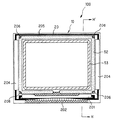
図1は、本発明の電気光学装置の一の実施の形態である液晶表示装置を、各構成要素とともに対向基板の側から見た平面図であり、図2は、図1のH−H’線における断面図である。図3は、電気光学装置(液晶表示装置)の画像表示領域においてマトリクス状に形成された複数の画素における各種素子、配線等の等価回路図である。なお、本形態の説明に用いた各図においては、各層や各部材を図面上で認識可能な程度の大きさとするため、各層や各部材毎に縮尺を異ならしめてある。
【0049】
図1及び図2において、本実施の形態の電気光学装置(液晶表示装置)100は、TFTアレイ基板10(第1の基板)と対向基板20(第2の基板)とがシール材52によって貼り合わされ、このシール材52によって区画された領域(液晶封入領域)内には、電気光学物質としての液晶50が封入、保持されている。シール材52の形成領域の内側の領域には、遮光性材料からなる周辺見切り53が形成されている。シール材52の外側の領域には、データ線駆動回路201、及び実装端子202がTFTアレイ基板10の一辺に沿って形成されており、この一辺に隣接する2辺に沿って走査線駆動回路204が形成されている。TFTアレイ基板10の残る一辺には、画像表示領域の両側に設けられた走査線駆動回路204の間を接続するための複数の配線205が設けられており、さらに、周辺見切り53の下側等を利用して、プリチャージ回路や検査回路が設けられることもある。また、対向基板20のコーナー部の少なくとも1箇所においては、TFTアレイ基板10と対向基板20との間で電気的導通をとるための基板間導通材206が配設されている。
【0050】
なお、データ線駆動回路201及び走査線駆動回路204をTFTアレイ基板10の上に形成する代わりに、例えば、駆動用LSIが実装されたTAB(テープ オートメイテッド ボンディング)基板とTFTアレイ基板10の周辺部に形成された端子群とを異方性導電膜を介して電気的及び機械的に接続するようにしてもよい。なお、電気光学装置100おいては、使用する液晶50の種類、すなわち、TN(ツイステッドネマティック)モード、STN(スーパーTN)モード等々の動作モードや、ノーマリホワイトモード/ノーマリブラックモードの別に応じて、偏光フィルム、位相差フィルム、偏光板等が所定の向きに配置されるが、ここでは図示を省略している。
【0051】
また、電気光学装置100をカラー表示用として構成する場合には、対向基板20において、TFTアレイ基板10の後述する各画素電極に対向する領域に、例えば、赤(R)、緑(G)、青(B)のカラーフィルタをその保護膜とともに形成する。
【0052】
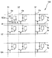
このような構造を有する電気光学装置100の画像表示領域においては、図3に示すように、複数の画素100aがマトリクス状に構成されているとともに、これらの画素100aの各々には、画素スイッチング用のTFT30が形成されており、画素信号S1、S2、・・・Snを供給するデータ線6aがTFT30のソースに電気的に接続されている。データ線6aに書き込む画素信号S1、S2、・・・Snは、この順に線順次で(線番号の順番で)供給してもよく、相隣接する複数のデータ線6a同士に対して、グループ毎に供給するようにしてもよい。また、TFT30のゲートには走査線3aが電気的に接続されており、所定のタイミングで、走査線3aにパルス的に走査信号G1、G2、・・・Gmをこの順に線順次で(線番号の順番で)印加するように構成されている。反射電極9及び透明電極8は、TFT30のドレインに電気的に接続されており、スイッチング素子であるTFT30を一定期間だけオン状態とすることにより、データ線6aから供給される画素信号S1、S2、・・・Snを各画素に所定のタイミングで書き込む。このようにして反射電極9及び透明電極8を介して液晶に書き込まれた所定レベルの画素信号S1、S2、・・・Snは、図2に示す対向基板20の対向電極21との間で一定期間保持される。
【0053】
ここで、液晶50は、印加される電圧レベルによって分子集合の配向や秩序が変化することにより、光を変調し、階調表示を可能にする。ノーマリホワイトモードであれば、印加された電圧に応じて入射光がこの液晶50の部分を通過する光量が低下し、ノーマリブラックモードであれば、印加された電圧に応じて入射光がこの液晶50の部分を通過する光量が増大する。その結果、全体として電気光学装置100からは画素信号S1、S2、・・・Snに応じたコントラストを持つ光が出射される。
【0054】
なお、保持された画素信号S1、S2、・・・Snがリークするのを防ぐために、反射電極9と対向電極との間に形成される液晶容量と並列に蓄積容量60(図3参照)を付加することがある。例えば、反射電極9及び透明電極8の電圧は、ソース電圧が印加された時間よりも3桁も長い時間だけ蓄積容量60により保持される。これにより、電荷の保持特性は改善され、コントラスト比の高い電気光学装置100を実現することができる。なお、蓄積容量60を形成する方法としては、図3に示すように、蓄積容量60を形成するための配線である容量線3bとの間に形成する場合、及び前段の走査線3aとの間に形成する場合のいずれであってもよい。
【0055】
(TFTアレイ基板の構成)
図4は、本実施の形態に用いたTFTアレイ基板の相互に隣接する複数の画素群の平面図である。図5は、図4のA−A’線における画素の断面図である。
【0056】
図4において、TFTアレイ基板上には、アルミニウムや銀、もしくはこれらの合金、又はチタン、窒化チタン、モリブデン、タンタル等との積層膜から構成された反射電極9がマトリクス状に形成されており(図4においては一画素を示す)、これら各反射電極9に対して、画素スイッチング用のTFT30(図3参照)がそれぞれ透明電極8を介して電気的に接続している。また、反射電極9を形成する領域の縦横の境界に沿って、データ線6a、走査線3a及び容量線3bが形成され、TFT30(図3参照)は、データ線6a及び走査線3aに対して接続している。すなわち、データ線6aは、コンタクト孔を介してTFT30(図3参照)の高濃度ソース領域1aに電気的に接続し、透明電極8は、コンタクト孔15及びソース線6bを介してTFT30(図3参照)の高濃度ドレイン領域1dに電気的に接続している。また、TFT30(図3参照)のチャネル形成用領域1a’に対向するように走査線3aが延びている。なお、蓄積容量60(蓄積容量素子)は、画素スイッチング用のTFT30(図3参照)を形成するための半導体膜1の延設部分1fを導電化したものを下電極とし、この下電極1fに、走査線3aと同層の容量線3bが上電極として重なった構造になっている。
【0057】
図4に示すように、このように構成した各画素100aにおいては、透過窓14を有する反射電極9が形成され、それらの表面には、後述する凹凸層(図示せず)が全面に形成されている。透過窓14に対応する領域は、透明電極8によって覆われ、透過モードで画像表示を行う透過領域であり、その他の領域は、後述する凹凸形成層(図示せず)、凹凸層(図示せず)及び反射電極9を備えた反射領域であり、ここでは反射モードで画像表示を行う。
【0058】
図5に示すように、この反射領域のA−A’線で切断したときの断面は、TFTアレイ基板10の基体としての透明なTFTアレイ基板用のガラス基板10’の表面に、厚さが100nm〜500nmのシリコン酸化膜(絶縁膜)からなる下地保護膜11が形成され、この下地保護膜11の表面には、厚さが30nm〜100nmの島状の半導体膜1が形成されている。半導体膜1の表面には、厚さが約50〜150nmのシリコン酸化膜からなるゲート絶縁膜2が形成され、このゲート絶縁膜2の表面に、厚さが300nm〜800nmの走査線3aがゲート電極として通っている。半導体膜1のうち、走査線3aに対してゲート絶縁膜2を介して対向する領域がチャネル形成用領域1a’になっている。このチャネル形成用領域1a’に対して一方側には、低濃度領域1b及び高濃度ソース領域1aを備えるソース領域が形成され、他方側には低濃度領域1b及び高濃度ドレイン領域1dを備えるドレイン領域が形成され、その中間には、ソース、ドレインのどちらの領域にも属さない高濃度領域1cが形成されている。
【0059】
画素スイッチング用のTFT30(図3参照)の表面側には、厚さが300nm〜800nmのシリコン酸化膜からなる第1層間絶縁膜4、及び厚さが100nm〜800nmのシリコン窒化膜からなる第2層間絶縁膜5(表面保護膜)が形成されている(この第2層間絶縁膜5(表面保護膜)は形成しなくてもよい)。第1層間絶縁膜4の表面には、厚さが300nm〜800nmのデータ線6aが形成され、このデータ線6aは、第1層間絶縁膜4に形成されたコンタクト孔を介して高濃度ソース領域1aに電気的に接続している。
【0060】
第2層間絶縁膜(表面保護膜)5の上層には、有機系樹脂等の感光性樹脂からなる凹凸形成層13及び凹凸層7がこの順に形成され、凹凸層7の表面には、ITO膜等からなる透明電極8が形成され、透明電極8の上層には、アルミニウムや銀、もしくはこれらの合金、又はチタン、窒化チタン、モリブデン、タンタル等との積層膜からなる反射電極9が順次形成されている。反射電極9の表面には、凹凸層7の表面凹凸形状に対応した凹凸パターン9gが形成されている。
【0061】
反射電極9及び透明電極8は、コンタクト孔15を介してソース線6bと電気的に接続している。
【0062】
反射電極9の表面には、背面光源からの光を透過するための透過窓14が形成されている。
【0063】
反射電極9の表面側と、透過窓14の形成によって最上層となった透明電極8の表面側にはポリイミド膜からなる配向膜12が形成されている。この配向膜12の表面側には、ラビング処理が施されている。
【0064】
また、高濃度ドレイン領域1dからの延設部分1f(下電極)に対しては、ゲート絶縁膜2と同時形成された絶縁膜(誘電体膜)を介して、走査線3aと同層の容量線3bが上電極として対向することにより、蓄積容量60(図3参照)が構成されている。
【0065】
なお、TFT30(図3参照)は、好ましくは上述のようにLDD構造(ライトリー・ドープト・ドレイン構造)をもつが、低濃度領域1bに相当する領域に不純物イオンの打ち込みを行わないオフセット構造を有していてもよい。また、TFT30(図3参照)は、ゲート電極(走査線3aの一部)をマスクとして高濃度で不純物イオンを打ち込み、自己整合的に高濃度のソース及びドレイン領域を形成したセルフアライン型のTFTであってもよい。
【0066】
また、本実施の形態では、TFT30(図3参照)のゲート電極(走査線3a)をソース−ドレイン領域の間に2個配置したデュアルゲート(ダブルゲート)構造としたが、1個配置したシングルゲート構造であってもよく、また、これらの間に3個以上のゲート電極を配置したトリプルゲート以上の構造であってもよい。複数個配置した場合、各々のゲート電極には同一の信号が印加されるようにする。このようにデュアルゲート(ダブルゲート)、又はトリプルゲート以上でTFT30(図3参照)を構成すれば、チャネルとソース−ドレイン領域の接合部でのリーク電流を防止でき、オフ時の電流を低減することができる。これらのゲート電極の少なくとも1個をLDD構造又はオフセット構造にすれば、さらに、オフ電流を低減でき、安定したスイッチング素子を得ることができる。
【0067】
図4〜図5において、TFTアレイ基板10では、各画素100aの反射領域には、反射電極9の表面のうち、TFT30(図3参照)の形成領域及びコンタクト孔15から外れた領域(凹凸層形成領域)には、前述のように凹凸パターン9gが形成されている。
【0068】
このような凹凸パターン9gを構成するにあたって、本実施の形態のTFTアレイ基板10では、前述の凹凸層形成領域には、アクリル樹脂等の有機系の透光性の感光性樹脂からなる凹凸形成層13が第2層間絶縁膜5の表面に1〜3μmの厚さで例えば、スピンコートによって形成され、この凹凸形成層13の上層には、アクリル樹脂等の有機系の透光性の感光性樹脂等のような流動性材料から形成された絶縁膜からなる凹凸層7が1〜2μmの厚さで例えば、スピンコートによって積層されている。
【0069】
凹凸形成層13には、多数の凹凸が形成されている。このため、図5に示すように、反射電極9の表面には、凹凸層7の表面凹凸形状に対応する凹凸パターン9gが形成され、この凹凸パターン9gでは、凹凸層7によって、凹凸形成層13のエッジ等が現れないようになっている。なお、凹凸層7を形成せずに、凹凸形成層13を形成した後、ベーク工程を行うことにより、凹凸形成層13の凹凸の縁を滑らかにしてもよい。
【0070】
(対向基板の構成)
図5において、対向基板20では、対向基板側のガラス基板20’上の、TFTアレイ基板10に形成されている反射電極9の縦横の境界領域と対向する領域にブラックマトリクス、又はブラックストライプ等と称せられる遮光膜23が形成され、その上層側には、ITO膜からなる対向電極21が形成されている。また、対向電極21の上層側には、ポリイミド膜からなる配向膜22が形成される。なお、TFTアレイ基板10と対向基板20との間には、液晶50が、保持、封入されている。
【0071】
(本形態の電気光学装置の作用)
このように構成した電気光学装置100(図1参照)では、アルミニウムや銀、もしくはこれらの合金、又はチタン、窒化チタン、モリブデン、タンタル等との積層膜からなる反射電極9が形成されているため、対向基板20側から入射した光をTFTアレイ基板10側で反射し、対向基板20側から出射することができるので、この間に液晶50によって各画素100a毎で光変調を行えば、外光を利用して所望の画像を表示することができる(反射モード)。
【0072】
また、電気光学装置100(図1参照)においては、図4〜図5において、反射電極9に設けられた透過窓14を覆うように透明電極8が形成されているため、透過型の液晶表示装置としても機能する。すなわち、TFTアレイ基板10の側に配置されたバックライト装置(図示せず)から出射された光は、TFTアレイ基板10の側に入射した後、各画素100aにおいて反射電極9が形成されている領域のうち、反射電極9が形成されていない透過領域(透明電極8によって覆われた透過窓14)を経由して対向基板20側に透過する。このため、液晶50によって各画素100a毎で光変調を行えば、バックライト装置(図示せず)から出射された光を利用して所望の画像を表示することができる(透過モード)。
【0073】
また、本実施の形態では、反射電極9の下層側のうち、反射電極9と平面的に重なる領域に凹凸形成層13を形成し、この凹凸形成層13の凹凸を利用して、反射電極9の表面に光散乱用の凹凸パターン9gを形成している。また、凹凸パターン9gでは、凹凸層7によって、凹凸形成層13のエッジ等が現れないようになっている。従って、反射モードで画像を表示したとき、散乱反射光で画像を表示するため、視野角依存性が小さい。
【0074】
さらに、透過窓14の部分にも配向膜12を十分に形成(塗布)して、かつ配向処理を十分に施すことが可能になり、画素内の透過モード表示におけるコントラストに優れるとともに、反射特性にも優れた電気光学装置を提供することができる。
【0075】
[TFTの製造方法]
このような構成のTFTアレイ基板10を製造する方法を、図6〜図10を参照しつつ、具体的に説明する。
【0076】
図6〜図10はいずれも、本実施の形態のTFTアレイ基板の製造方法を工程順に示す断面図である。
【0077】
まず、図6(A)に示すように、超音波洗浄等により清浄化したTFTアレイ基板用のガラス基板10’を準備した後、基板温度が150℃〜450℃の温度条件下で、TFTアレイ基板用のガラス基板10’の全面に、シリコン酸化膜からなる下地保護膜11をプラズマCVD法により100nm〜500nmの厚さに形成する。このときの原料ガスとしては、例えば、モノシランと笑気ガス(一酸化二窒素)との混合ガスやTEOS(テトラエトキシシラン:Si(OC2H5)4)と酸素、又はジシランとアンモニアを用いることができる。
【0078】
次に、基板温度が150℃〜450℃の温度条件下で、TFTアレイ基板用のガラス基板10’の全面に、非晶質シリコン膜からなる半導体膜1をプラズマCVD法により30nm〜100nmの厚さに形成する。このときの原料ガスとしては、例えば、ジシランやモノシランを用いることができる。次に、半導体膜1に対してレーザ光を照射してレーザアニールを施す。その結果、アモルファスの半導体膜1は、一度溶融し、冷却固化過程を経て結晶化する。この際には、各領域へのレーザ光の照射時間が非常に短時間であり、かつ、照射領域も基板全体に対して局所的であるため、基板全体が同時に高温に熱せられることがない。それゆえ、TFTアレイ基板用のガラス基板10’としてガラス基板等を用いても熱による変形や割れ等が生じない。
【0079】
次に、半導体膜1の表面にフォトリソグラフィ技術を用いてレジストマスク551を介して半導体膜1をエッチングすることにより、図6(B)に示すように、島状の半導体膜1(能動層)を形成するための半導体膜を各々分離した状態に形成する。
【0080】
次に、350℃以下の温度条件下で、TFTアレイ基板用のガラス基板10’の全面に、CVD法等により半導体膜1の表面に、シリコン酸化膜等からなるゲート絶縁膜2を50nm〜150nmの厚さに形成する。このときの原料ガスは、例えば、TEOSと酸素ガスとの混合ガスを用いることができる。ここで形成するゲート絶縁膜2は、シリコン酸化膜に代えてシリコン窒化膜であってもよい。
【0081】
次に、図示を省略するが、所定のレジストマスクを介して半導体膜1の延設部分1fに不純物イオンを打ち込んで、容量線3bとの間に蓄積容量60を構成するための下電極を形成する(図4及び図5参照)。
【0082】
次に、図6(C)に示すように、スパッタ法等により、TFTアレイ基板用のガラス基板10’の全面に、走査線3a等を形成するためのアルミニウム、タンタル、モリブデン等からなる金属膜、又はこれらの金属のいずれかを主成分とする合金膜からなる導電膜3を300nm〜800nmの厚さに形成した後、フォトリソグラフィ技術を用いてレジストマスク552を形成する。
【0083】
次に、レジストマスクを介して導電膜3をドライエッチングし、図6(D)に示すように、走査線3a(ゲート電極)、容量線3b等を形成する。
【0084】
次に、画素TFT部及び駆動回路のNチャネルTFT部(図示せず)の側には、走査線3aやゲート電極をマスクとして、約0.1×10¹³/cm2〜約10×1013/cm2のドーズ量で低濃度の不純物イオン(リンイオン)を打ち込んで、走査線3aに対して自己整合的に低濃度領域1bを形成する。ここで、走査線3aの真下に位置しているため、不純物イオンが導入されなかった部分は半導体膜1のままのチャネル形成用領域1a’となる。
【0085】
次に、図7(A)に示すように、画素TFT部では、走査線3a(ゲート電極)より幅の広いレジストマスク553を形成して高濃度の不純物イオン(リンイオン)を約0.1×10¹⁵/cm2〜約10×1015/cm2のドーズ量で打ち込み、高濃度ソース領域1a、高濃度領域1c及び高濃度ドレイン領域1dを形成する。
【0086】
これらの不純物導入工程に代えて、低濃度の不純物の打ち込みを行わずにゲート電極より幅の広いレジストマスクを形成した状態で高濃度の不純物(リンイオン)を打ち込み、オフセット構造のソース領域及びドレイン領域を形成してもよい。また、走査線3aをマスクにして高濃度の不純物を打ち込んで、セルフアライン構造のソース領域及びドレイン領域を形成してもよい。
【0087】
なお、図示を省略するが、このような工程によって、周辺駆動回路部のNチャネルTFT部を形成するが、この際には、PチャネルTFT部をマスクで覆っておく。また、周辺駆動回路のPチャネルTFT部を形成する際には、画素部及びNチャネルTFT部をレジストで被覆保護して、ゲート電極をマスクとして、約0.1×10¹⁵/cm2〜約10×1015/cm2のドーズ量でボロンイオンを打ち込むことにより、自己整合的にPチャネルのソース−ドレイン領域を形成する。
【0088】
この際、NチャネルTFT部の形成時と同様、ゲート電極をマスクとして、約0.1×10¹³/cm2〜約10×1013/cm2のドーズ量で低濃度の不純物(ボロンイオン)を導入して、ポリシリコン膜に低濃度領域を形成した後、ゲート電極より幅の広いマスクを形成して高濃度の不純物(ボロンイオン)を約0.1×1015/cm2〜約10×1015/cm2のドーズ量で打ち込んで、LDD構造のソース領域及びドレイン領域を形成してもよい。また、低濃度の不純物の打ち込みを行わずに、ゲート電極より幅の広いマスクを形成した状態で高濃度の不純物(ボロンイオン)を打ち込み、オフセット構造のソース領域及びドレイン領域を形成してもよい。これらのイオン打ち込み工程によって、CMOS化(相補型化:Complimentary MOS化)が可能になり、周辺駆動回路の同一基板内への内蔵が可能になる。
【0089】
次に、図7(B)に示すように、走査線3aの表面側にCVD法等により、シリコン酸化膜等からなる層間絶縁膜4を300nm〜800nmの厚さに形成する。このときの原料ガスは、例えば、TEOSと酸素ガスとの混合ガスを用いることができる。
【0090】
次に、フォトリソグラフィ技術を用いてレジストマスク554を形成する。
【0091】
次に、レジストマスク554を介して層間絶縁膜4にドライエッチングを行い、図7(C)に示すように、層間絶縁膜4においてソース領域及びドレイン領域に対応する部分等にコンタクト孔をそれぞれ形成する。
【0092】
次に、図7(D)に示すように、層間絶縁膜4の表面側に、データ線6a(ソース電極)等を構成するためのアルミニウム膜、チタン膜、窒化チタン膜、タンタル膜、モリブデン膜、又はこれらの金属のいずれかを主成分とする合金膜又は積層膜からなる金属膜6をスパッタ法等で400nm〜800nmの厚さに形成した後、フォトリソグラフィ技術を用いてレジストマスク555を形成する。
【0093】
次に、レジストマスク555を介して金属膜6にドライエッチングを行い、図8(A)に示すように、データ線6a、及びソース線6bを形成する。
【0094】
次に、図8(B)に示すように、シリコン窒化膜からなる第2層間絶縁膜5を、データ線6a、及びソース線6bの表面側にCVD法等により、100nm〜800nmの膜厚に形成する。
【0095】
次に、図9(A)、(B)に示すように、アクリル樹脂等の有機系の透光性の感光性樹脂13aを1〜3μmの厚さにスピンコートで塗布した後、感光性樹脂13aをフォトリソグラフィ技術を用いてパターニングすることによって、厚さが1μm〜3μmの凹凸形成層13を形成する。次いで、角をとるためベーク工程を行ってもよい。
【0096】
このようなフォトリソグラフィ技術を利用して凹凸形成層13を形成する際、透光性の感光性樹脂13aとしてはネガタイプ及びポジタイプのいずれを用いてもよいが、図9(A)には、感光性樹脂13aとしてポジタイプを用いた場合を例示してあり、感光性樹脂13aを除去したい部分に対して、所定の露光マスクの透光部分を介して紫外線を照射する。
【0097】
次に、図9(C)に示すように、透明電極8及び凹凸形成層13の表面側に、アクリル樹脂等の有機系の透光性の感光性樹脂7aをスピンコートで1μm〜2μmの厚さに塗布する。
【0098】
次に、図9(D)に示すように、フォトリソグラフィ技術を利用して、感光性樹脂7a(図9(C)参照)をソース線6bの表面に達するまで貫通、開口させて、後述するコンタクト孔15を形成することができるように開口14bを形成するとともに、この開口14bを備えた厚さが1μm〜2μmの凹凸層7を形成する。
【0099】
ここで、凹凸層7は、流動性を有する材料を塗布したものから形成されるため、凹凸層7の表面には、凹凸形成層13の凹凸を適度に打ち消して、エッジ等のない、滑らかな形状の凹凸パターンが形成される。
【0100】
なお、凹凸層7を形成せずに、滑らかな形状の凹凸パターンを形成する場合には、図9(B)に示す状態でベーク工程を行って、凹凸形成層13の縁を滑らかな形状にしてもよい。
【0101】
次に、図10(A)に示すように、凹凸層7及びコンタクト孔15の表面に、スパッタリング法等によって、約50〜200nmの厚さのITOからなる透明導電膜を成膜し、フォトリソグラフィ技術及びエッチング技術を用いて、所定のパターンの透明電極8を形成する。透明電極8の表面に、アルミニウムや銀、もしくはこれらの合金、又はチタン、窒化チタン、モリブデン、タンタル等との積層膜のような反射性を備えた金属膜9aを形成する。
【0102】
次に、図10(B)に示すように、フォトリソグラフィ技術及びエッチング技術を用いて、透過窓14となる部分及び隣接する画素との間を選択的に除去して、透過窓14を備えた反射電極9を形成する。このようにして形成した反射電極9は、透明電極8を介してドレイン電極6bと電気的に接続している。また、反射電極9の表面には、凹凸形成層13及び凹凸層7からなる凹凸によって500nm以上、さらには800nm以上の凹凸パターン9gが形成され、かつ、この凹凸パターン9gは、凹凸層7によって、エッジ等のない、滑らかな形状になっている。
【0103】
その後、反射電極9と、透過窓14の形成によって最上層となった透明電極8との表面側に配向膜(ポリイミド膜)12を形成する。それには、ブチルセロソルブやn−メチルピロリドン等の溶媒に5〜10重量%のポリイミドやポリアミド酸を溶解させたポリイミド・ワニスをフレキソ印刷した後、加熱・硬化(焼成)する。そして、ポリイミド膜を形成した基板をレーヨン系繊維からなるパフ布で一定方向に擦り、ポリイミド分子を表面近傍で一定方向に配列させる(ラビング処理を施す)。その結果、後で充填した液晶分子とポリイミド分子との相互作用により液晶分子が一定方向に配列する。
【0104】
以上のようにして、TFTアレイ基板10が完成する。
【0105】
上記のいずれの形態も、画素スイッチング素子としてTFTを用いたアクティブマトリクス型の液晶表示装置を例に説明したが、画素スイッチング素子としてTFDを用いたアクティブマトリクス型の液晶表示装置、又はパッシブマトリクス型の液晶表示装置、さらには液晶以外の電気光学物質(例えば、EL発光素子)を用いた電気光学装置に本発明を適用してもよい。
【0106】
[電気光学装置の電子機器への応用]
このように構成した半反射・半透過型の電気光学装置100は、各種の電子機器の表示部として用いることができるが、その一例を、図11〜図13を参照しつつ具体的に説明する。
【0107】
図11は、本発明に係る電気光学装置を表示装置として用いた電子機器の回路構成を示すブロック図である。
【0108】
図11において、電子機器は、表示情報出力源70、表示情報処理回路71、電源回路72、タイミングジェネレータ73及び液晶表示装置74を有する。また、液晶表示装置74は、液晶表示パネル75及び駆動回路76を有する。液晶装置74としては、前述した電気光学装置100を用いることができる。
【0109】
表示情報出力源70は、ROM(Read Only Memory)、RAM(Random Access Memory)等のようなメモリ、各種ディスク等のようなストレージユニット、デジタル画像信号を同調出力する同調回路等を備え、タイミングジェネレータ73によって生成された各種のクロック信号に基づいて、所定フォーマットの画像信号等のような表示情報を表示情報処理回路71に供給する。
【0110】
表示情報処理回路71は、シリアル−パラレル変換回路や、増幅・反転回路、ローテーション回路、ガンマ補正回路、クランプ回路等のような周知の各種回路を備え、入力した表示情報の処理を実行して、その画像信号をクロック信号CLKとともに駆動回路76へ供給する。電源回路72は、各構成要素に所定の電圧を供給する。
【0111】
図12は、本発明に係る電子機器の一実施形態であるモバイル型のパーソナルコンピュータを示している。ここに示すパーソナルコンピュータ80は、キーボード81を備えた本体部82と、液晶表示ユニット83とを有する。液晶表示ユニット83は、前述した電気光学装置100を含んで構成される。
【0112】
図13は、他の電子機器である携帯電話機を示している。ここに示す携帯電話機90は、複数の操作ボタン91と、前述した電気光学装置100からなる表示部とを有している。
【0113】
【発明の効果】
以上、説明したように、本発明によって、携帯電話機、モバイルコンピュータ等に好適に用いられる、透過窓の部分にも配向処理が十分に施された、画素内の透過モード表示におけるコントラストに優れるとともに、反射特性にも優れた電気光学装置及びその製造方法を提供することができる。
【図面の簡単な説明】
【図1】本発明の電気光学装置の一の実施の形態を対向基板の側から見たときの平面図である。
【図2】図1のH−H’線における断面図である。
【図3】本発明の電気光学装置の一の実施の形態において、マトリクス状に配置された複数の画素に形成された各種素子、配線等の等価回路図である。
【図4】本発明の電気光学装置の一の実施の形態において、TFTアレイ基板に形成された各画素の構成を示す平面図である。
【図5】図4のA−A’線における画素の断面図である。
【図6】本発明の電気光学装置の製造方法の一の実施の形態において、TFTアレイ基板の製造方法を工程順に示す断面図である。
【図7】図6に示す工程以降のTFTアレイ基板の製造方法を工程順に示す断面図である。
【図8】図7に示す工程以降のTFTアレイ基板の製造方法を工程順に示す断面図である。
【図9】図8に示す工程以降のTFTアレイ基板の製造方法を工程順に示す断面図である。
【図10】図9に示す工程以降のTFTアレイ基板の製造方法を工程順に示す断面図である。
【図11】本発明に係る電気光学装置を表示装置として用いた電子機器の回路構成を示すブロック図である。
【図12】本発明の電気光学装置を用いた電子機器の一例としてのモバイル型のパーソナルコンピュータを示す説明図である。
【図13】本発明の電気光学装置を用いた電子機器の他の例としての携帯電話機の説明図である。
【図14】従来の電気光学装置における画素の一部を模式的に示す説明図であって、(A)は平面図、(B)は(A)のC−C’における断面図である。
【符号の説明】
1…半導体膜
1a…高濃度ソース領域
1a’…チャネル形成用領域
1b…低濃度領域
1c…高濃度領域
1d…高濃度ドレイン領域
1f…半導体膜の延設部分
2…ゲート絶縁膜
3a…走査線
3b…容量線
4…第1層間絶縁膜
5…第2層間絶縁膜(表面保護膜)
6…金属膜
6a…データ線
6b…ソース線
7…凹凸層
7a…凹凸層を形成するための感光性樹脂
8…透明電極
9…反射電極
9a…金属膜
9g…凹凸パターン(表面凹凸形状)
10…TFTアレイ基板
10’…TFTアレイ基板側のガラス基板
11…下地保護膜
12…配向膜
13…凹凸形成層
13a…凹凸形成層を形成するための感光性樹脂
14…透過窓
14a…スリット形状の透過窓
14b…凹凸層の開口
15…コンタクト孔
20…対向基板
20’…対向基板側のガラス基板
21…対向電極
22…配向膜
30…画素スイッチング用のTFT
50…液晶
52…シール材
53…周辺見切り
60…蓄積容量
70…表示情報出力源
71…表示情報処理回路
72…電源回路
73…タイミングジェネレータ
74…液晶表示装置
75…液晶表示パネル
76…駆動回路
80…パーソナルコンピュータ
81…キーボード
82…本体部
83…液晶表示ユニット
90…携帯電話機
91…操作ボタン
100…電気光学装置
100a…画素
101…基板
102…下地保護膜
103…透明電極
104…保護膜
105…凹凸形成層
106…凹凸層
107…透過窓
108…反射電極
109…反射用の凹凸
110…画素
120…TFTアレイ基板
201…データ線駆動回路
202…実装端子
204…走査線駆動回路
205…配線
206…基板間導通材[0001]
BACKGROUND OF THE INVENTION
The present invention relates to an electro-optical device and a manufacturing method thereof. More specifically, an electro-optic that is suitably used for a mobile phone, a mobile computer, etc., is sufficiently subjected to orientation processing on the transmissive window portion, and has excellent contrast in transmissive mode display in a pixel and excellent in reflection characteristics. The present invention relates to an apparatus and a manufacturing method thereof.
[0002]
[Prior art]
Electro-optical devices (for example, liquid crystal display devices, EL light-emitting display devices, etc.) are widely used as direct-view display devices for various devices such as mobile phones and mobile computers. Among such electro-optical devices, for example, in an active matrix type, semi-transmissive / semi-reflective liquid crystal display device, a TFT array substrate and a counter substrate which are arranged to face each other are bonded together with a sealing material, Liquid crystal as an electro-optical material is sealed and held in a region partitioned by a sealing material between the substrates.
[0003]
In addition, a reflective electrode is formed on the surface of the TFT array substrate to reflect external light incident from the counter substrate side in the direction of the counter substrate, and the light incident from the counter substrate side is reflected by the TFT array substrate. An image is displayed by light reflected from the electrode and emitted from the counter substrate side (reflection mode). In addition, a transparent electrode is formed on the reflective electrode to transmit light, and a transparent electrode is formed on the lower layer side of the reflective electrode so as to cover the transparent window, and light from the backlight is transmitted by the light transmitted through the transparent window. Display an image (transparent mode).
[0004]
As a
[0005]
[Problems to be solved by the invention]
The liquid crystal display device using the reflective electrode having such a configuration is capable of providing a liquid crystal display device having excellent visibility without being affected by the brightness of external light. Since the film thickness of the concavo-convex forming
[0006]
The present invention has been made in view of the above-described problems, and the alignment processing is sufficiently performed on the transmissive window portion, and the contrast in the transmissive mode display in the pixel is excellent, and the reflection characteristics are also excellent. An object of the present invention is to provide an electro-optical device and a manufacturing method thereof.
[0007]
[Means for Solving the Problems]
In order to achieve the above object, the electro-optical device of the present invention includes:In an electro-optical device having an image display area including a plurality of pixels, and each of the plurality of pixels including a reflective area that reflects incident light and a transmissive area that transmits incident light, the reflective area is reflective. A transparent electrode is formed at least in the transmissive region, and an alignment film is formed on the metal film and the transparent electrode in both the reflective region and the transmissive region. The concavo-convex pattern that makes the surface of the metal film concavo-convex shape is formed under the metal film and the transparent electrode, and the convex portion of the concavo-convex pattern is disposed so as not to straddle the boundary portion between the transmission region and the reflection region, The area where the transparent electrode is formed is wider than the area where the metal film is formedIt is characterized by that.
The metal film is preferably formed on the surface of the transparent electrode.
The concave / convex pattern includes a first formation layer that is a base of the convex portion and a second formation layer that covers the first formation layer, and the second formation layer has an edge in the first formation layer that does not appear in the concave / convex pattern. It is preferable to be formed as follows.
Each of the plurality of pixels has a switching TFT and a storage capacitor for holding a voltage applied to the pixel electrode. The TFT and the storage capacitor are formed in the reflection region. It is preferable that only the second formation layer is stacked in the region where the storage capacitor is formed.
[0008]
By configuring in this way, the surface of the reflective electrode is provided with a surface uneven shape (reflection unevenness) that scatters reflected light appropriately, and an alignment film is sufficiently formed (applied) on the transmission window portion. Thus, it is possible to sufficiently perform the alignment treatment, and it is possible to provide an electro-optical device that is excellent in contrast in transmissive mode display in a pixel and excellent in reflection characteristics.
[0009]
In the electro-optical device according to the aspect of the invention, the convex portion of the concavo-convex layer is located either inside or outside the boundary portion without straddling the boundary portion between the region corresponding to the transmission window and the other region. It is preferable to be arranged as described above.
[0010]
With this configuration, when a transmissive window is formed on the reflective electrode using photolithography technology and etching technology, it is possible to effectively prevent an etchant or the like from entering between the reflective electrode and the uneven layer. it can.
[0011]
In the electro-optical device according to the aspect of the invention, it is preferable that the uneven layer is formed of a light-transmitting photosensitive resin.
[0012]
With this configuration, the manufacturing process can be made more efficient, and the reduction in transmission characteristics can be prevented.
[0013]
In the electro-optical device according to the aspect of the invention, it is preferable that a concavo-convex forming layer is further disposed on the lower layer side of the concavo-convex layer.
[0014]
By comprising in this way, the uneven | corrugated layer which has a smooth surface uneven | corrugated shape with few edges and a flat part can be formed easily.
[0015]
In the electro-optical device according to the aspect of the invention, it is preferable that the unevenness forming layer is formed of a light-transmitting photosensitive resin.
[0016]
By comprising in this way, the uneven | corrugated layer which has a surface uneven | corrugated shape of a desired magnitude | size can be efficiently formed in a desired position.
[0017]
In the electro-optical device according to the aspect of the invention, it is preferable that the reflective electrode is composed of aluminum, silver, or an alloy thereof, or a laminated film of titanium, titanium nitride, molybdenum, tantalum, or the like.
[0018]
By configuring in this way, the light reflection efficiency can be increased.
[0019]
In the electro-optical device according to the aspect of the invention, it is preferable that the transparent electrode is composed of an ITO film.
[0020]
With this configuration, the contrast in the transmissive mode display can be increased.
[0021]
In the electro-optical device according to the aspect of the invention, it is preferable that a region where the transparent electrode is formed is wider than a region where the reflective electrode is formed.
[0022]
With this configuration, the contrast in the transmissive mode display can be increased.
[0023]
In the electro-optical device according to the aspect of the invention, it is preferable that the transparent electrode and the reflective electrode are electrically connected.
[0024]
With this configuration, power consumption can be reduced.
[0025]
In the electro-optical device according to the aspect of the invention, it is preferable that the transparent electrode is electrically connected to a potential supply line outside the transmission window.
[0026]
With this configuration, power consumption can be reduced.
[0027]
In addition, the manufacturing method of the electro-optical device of the present invention includes:In a method of manufacturing an electro-optical device having an image display area including a plurality of pixels, each of the pixels including a reflection area that reflects incident light and a transmission area that transmits incident light. A step of forming a first forming layer, a step of forming a second forming layer covering the first forming layer so that an edge of the first forming layer does not appear on the surface, and the first forming layer and the first forming layer. Forming a transparent electrode on the concavo-convex pattern comprising: forming a metal film on the surface of the transparent electrode; forming a reflective electrode having a transparent region that includes the etching of the metal film and exposes the transparent electrode And a step of forming an alignment film in both the reflective region and the transmissive region, and the convex portion of the concavo-convex pattern is disposed so as not to straddle the boundary portion between the transmissive region and the reflective region. RuIt is characterized by that.
[0028]
With this configuration, the surface of the reflective electrode has a surface irregularity shape (reflection irregularity) that scatters reflected light in an appropriate manner, providing excellent contrast in transmissive mode display within the pixel and excellent reflection characteristics. In addition, the electro-optical device can be provided efficiently and at low cost.
[0029]
In this case, the convex portion of the concave-convex layer is disposed so as to be located either inside or outside the boundary portion without straddling the boundary portion between the region corresponding to the transmission window and the other region. Is preferred.
[0030]
With this configuration, when a transmissive window is formed on the reflective electrode using photolithography technology and etching technology, it is possible to effectively prevent an etchant or the like from entering between the reflective electrode and the uneven layer. it can.
[0031]
In the electro-optical device manufacturing method according to the aspect of the invention, it is preferable that the uneven layer is formed of a light-transmitting photosensitive resin.
[0032]
With this configuration, the manufacturing process can be made more efficient, and the reduction in transmission characteristics can be prevented.
[0033]
In the method of manufacturing the electro-optical device according to the aspect of the invention, it is preferable that a concavo-convex forming layer is further disposed on the lower layer side of the concavo-convex layer.
[0034]
By comprising in this way, the uneven | corrugated layer which has a smooth surface uneven | corrugated shape with few edges and a flat part can be formed efficiently and at low cost.
[0035]
In the method for manufacturing the electro-optical device according to the aspect of the invention, it is preferable that the unevenness forming layer is formed from a light-transmitting photosensitive resin.
[0036]
By comprising in this way, the uneven | corrugated layer which has a surface uneven | corrugated shape of a desired magnitude | size can be efficiently formed at a desired position at low cost.
[0037]
In the electro-optical device manufacturing method of the present invention, it is preferable that the reflective electrode is made of aluminum, silver, or an alloy thereof, or a laminated film of titanium, titanium nitride, molybdenum, tantalum, or the like.
[0038]
With this configuration, an electro-optical device with high light reflection efficiency can be provided efficiently and at low cost.
[0039]
In the electro-optical device manufacturing method of the present invention, it is preferable that the transparent electrode is made of an ITO film.
[0040]
With this configuration, an electro-optical device with high contrast in transmissive mode display can be provided efficiently and at low cost.
[0041]
In the method of manufacturing the electro-optical device according to the aspect of the invention, it is preferable that a region where the transparent electrode is formed is wider than a region where the reflective electrode is formed.
[0042]
With this configuration, an electro-optical device with high contrast in transmissive mode display can be provided efficiently and at low cost.
[0043]
In the method for manufacturing the electro-optical device according to the aspect of the invention, it is preferable that the transparent electrode and the reflective electrode are electrically connected.
[0044]
With this configuration, an electro-optical device with reduced power consumption can be provided efficiently and at low cost.
[0045]
In the method of manufacturing the electro-optical device according to the aspect of the invention, it is preferable that the transparent electrode is electrically connected to a potential supply line outside the transmission window.
[0046]
With this configuration, an electro-optical device with reduced power consumption can be provided efficiently and at low cost.
[0047]
DETAILED DESCRIPTION OF THE INVENTION
Embodiments of an electro-optical device and a manufacturing method thereof according to the present invention will be specifically described below with reference to the drawings.
[0048]
(Basic configuration of electro-optical device)
FIG. 1 is a plan view of a liquid crystal display device according to an embodiment of the electro-optical device of the present invention as viewed from the counter substrate side together with each component, and FIG. It is sectional drawing in a line. FIG. 3 is an equivalent circuit diagram of various elements and wirings in a plurality of pixels formed in a matrix in the image display region of the electro-optical device (liquid crystal display device). Note that, in each drawing used in the description of the present embodiment, each layer and each member have different scales so that each layer and each member can be recognized on the drawing.
[0049]
1 and 2, the electro-optical device (liquid crystal display device) 100 according to the present embodiment has a TFT array substrate 10 (first substrate) and a counter substrate 20 (second substrate) attached by a sealing
[0050]
Instead of forming the data line driving
[0051]
In the case where the electro-
[0052]
In the image display area of the electro-
[0053]
Here, the
[0054]
In order to prevent the retained pixel signals S1, S2,... Sn from leaking, a storage capacitor 60 (see FIG. 3) is provided in parallel with the liquid crystal capacitor formed between the
[0055]
(Configuration of TFT array substrate)
FIG. 4 is a plan view of a plurality of pixel groups adjacent to each other on the TFT array substrate used in the present embodiment. FIG. 5 is a cross-sectional view of the pixel taken along line A-A ′ of FIG. 4.
[0056]
In FIG. 4, on the TFT array substrate, reflecting
[0057]
As shown in FIG. 4, in each
[0058]
As shown in FIG. 5, the cross-section of the reflection region taken along the line AA ′ has a thickness on the surface of a
[0059]
On the surface side of the pixel switching TFT 30 (see FIG. 3), a first
[0060]
On the upper surface of the second interlayer insulating film (surface protective film) 5, a concavo-convex forming
[0061]
The
[0062]
A
[0063]
An
[0064]
Further, the
[0065]
The TFT 30 (see FIG. 3) preferably has an LDD structure (lightly doped drain structure) as described above, but has an offset structure in which impurity ions are not implanted into a region corresponding to the
[0066]
In this embodiment, a dual gate (double gate) structure in which two gate electrodes (
[0067]
4 to 5, in the
[0068]
In constructing such a concavo-
[0069]
A large number of irregularities are formed in the
[0070]
(Configuration of counter substrate)
In FIG. 5, in the
[0071]
(Operation of the electro-optical device of this embodiment)
In the electro-optical device 100 (see FIG. 1) configured as described above, the
[0072]
Further, in the electro-optical device 100 (see FIG. 1), since the
[0073]
Further, in the present embodiment, the concavo-convex forming
[0074]
Further, the
[0075]
[TFT manufacturing method]
A method of manufacturing the
[0076]
6 to 10 are all cross-sectional views showing the manufacturing method of the TFT array substrate of this embodiment in the order of steps.
[0077]
First, as shown in FIG. 6 (A), after preparing a
[0078]
Next, the
[0079]
Next, the
[0080]
Next, under a temperature condition of 350 ° C. or less, a
[0081]
Next, although not shown, impurity ions are implanted into the
[0082]
Next, as shown in FIG. 6C, a metal film made of aluminum, tantalum, molybdenum or the like for forming the
[0083]
Next, the conductive film 3 is dry-etched through a resist mask to form a
[0084]
Next, on the side of the pixel TFT portion and the N-channel TFT portion (not shown) of the driving circuit, about 0.1 × 10 6 using the
[0085]
Next, as shown in FIG. 7A, in the pixel TFT portion, a resist
[0086]
Instead of these impurity introduction steps, a high concentration impurity (phosphorus ion) is implanted in a state where a resist mask wider than the gate electrode is formed without implanting the low concentration impurity, and the source region and drain region of the offset structure May be formed. Alternatively, a source region and a drain region having a self-aligned structure may be formed by implanting high concentration impurities using the
[0087]
Although not shown, the N-channel TFT portion of the peripheral drive circuit portion is formed by such a process. In this case, the P-channel TFT portion is covered with a mask. Further, when forming the P-channel TFT portion of the peripheral drive circuit, the pixel portion and the N-channel TFT portion are covered and protected with a resist, and the gate electrode is used as a mask to provide about 0.1 × 10¹⁵/ Cm2~ About 10 × 1015/ Cm2By implanting boron ions with a dose amount of P, a P-channel source-drain region is formed in a self-aligned manner.
[0088]
At this time, similarly to the formation of the N-channel TFT portion, about 0.1 × 10 10 using the gate electrode as a mask.13/ Cm2~ About 10 × 1013/ Cm2After introducing a low concentration impurity (boron ions) at a dose of a low concentration region in the polysilicon film, a mask wider than the gate electrode is formed to reduce the high concentration impurities (boron ions). 0.1 × 10¹⁵/ Cm2~ About 10 × 1015/ Cm2The source region and the drain region of the LDD structure may be formed by implanting with a dose amount of. Alternatively, a source region and a drain region having an offset structure may be formed by implanting high-concentration impurities (boron ions) in a state where a mask wider than the gate electrode is formed without implanting low-concentration impurities. . By these ion implantation processes, CMOS (complementary: Complementary MOS) can be realized, and a peripheral drive circuit can be built in the same substrate.
[0089]
Next, as shown in FIG. 7B, an
[0090]
Next, a resist
[0091]
Next, dry etching is performed on the
[0092]
Next, as shown in FIG. 7D, an aluminum film, a titanium film, a titanium nitride film, a tantalum film, and a molybdenum film for forming the
[0093]
Next, dry etching is performed on the metal film 6 through the resist
[0094]
Next, as shown in FIG. 8B, the second
[0095]
Next, as shown in FIGS. 9A and 9B, an organic translucent photosensitive resin 13a such as an acrylic resin is applied to a thickness of 1 to 3 μm by spin coating, and then the photosensitive resin is applied. The concavo-
[0096]
When the concavo-convex forming
[0097]
Next, as shown in FIG. 9C, an organic translucent photosensitive resin 7a such as an acrylic resin is spin coated on the surface side of the
[0098]
Next, as shown in FIG. 9D, the photosensitive resin 7a (see FIG. 9C) is penetrated and opened until reaching the surface of the
[0099]
Here, since the concavo-
[0100]
In addition, when forming a concavo-convex pattern with a smooth shape without forming the concavo-
[0101]
Next, as shown in FIG. 10A, a transparent conductive film made of ITO having a thickness of about 50 to 200 nm is formed on the surface of the concavo-
[0102]
Next, as illustrated in FIG. 10B, the
[0103]
Thereafter, an alignment film (polyimide film) 12 is formed on the surface side of the
[0104]
As described above, the
[0105]
In any of the above embodiments, an active matrix type liquid crystal display device using TFT as a pixel switching element has been described as an example. However, an active matrix type liquid crystal display device using TFD as a pixel switching element, or a passive matrix type liquid crystal display device. The present invention may be applied to a liquid crystal display device, and an electro-optical device using an electro-optical material other than liquid crystal (for example, an EL light emitting element).
[0106]
[Application of electro-optical device to electronic equipment]
The semi-reflective / semi-transmissive electro-
[0107]
FIG. 11 is a block diagram illustrating a circuit configuration of an electronic apparatus using the electro-optical device according to the invention as a display device.
[0108]
In FIG. 11, the electronic device includes a display
[0109]
The display
[0110]
The display
[0111]
FIG. 12 shows a mobile personal computer which is an embodiment of the electronic apparatus according to the present invention. The
[0112]
FIG. 13 illustrates a mobile phone which is another electronic device. A cellular phone 90 shown here includes a plurality of operation buttons 91 and a display unit including the electro-
[0113]
【The invention's effect】
As described above, according to the present invention, the present invention is suitable for a mobile phone, a mobile computer, etc. An electro-optical device excellent in reflection characteristics and a method for manufacturing the same can be provided.
[Brief description of the drawings]
FIG. 1 is a plan view of an electro-optical device according to an embodiment of the present invention as viewed from a counter substrate side.
FIG. 2 is a cross-sectional view taken along line H-H ′ of FIG.
FIG. 3 is an equivalent circuit diagram of various elements and wirings formed in a plurality of pixels arranged in a matrix in an embodiment of the electro-optical device of the invention.
FIG. 4 is a plan view showing a configuration of each pixel formed on a TFT array substrate in one embodiment of the electro-optical device of the invention.
5 is a cross-sectional view of a pixel taken along line A-A ′ in FIG. 4;
6 is a cross-sectional view showing a method of manufacturing a TFT array substrate in the order of steps in an embodiment of a method of manufacturing an electro-optical device according to the invention. FIG.
7 is a cross-sectional view showing a method of manufacturing a TFT array substrate subsequent to the step shown in FIG. 6 in the order of steps.
8 is a cross-sectional view showing a method of manufacturing the TFT array substrate after the step shown in FIG. 7 in order of steps.
9 is a cross-sectional view showing a method of manufacturing the TFT array substrate subsequent to the step shown in FIG. 8 in order of steps.
10 is a cross-sectional view showing a method of manufacturing the TFT array substrate after the step shown in FIG. 9 in order of steps.
FIG. 11 is a block diagram illustrating a circuit configuration of an electronic apparatus using the electro-optical device according to the invention as a display device.
FIG. 12 is an explanatory diagram illustrating a mobile personal computer as an example of an electronic apparatus using the electro-optical device of the invention.
FIG. 13 is an explanatory diagram of a mobile phone as another example of an electronic apparatus using the electro-optical device of the invention.
14A and 14B are explanatory views schematically showing a part of a pixel in a conventional electro-optical device, in which FIG. 14A is a plan view and FIG. 14B is a sectional view taken along line C-C ′ in FIG.
[Explanation of symbols]
1 ... Semiconductor film
1a: High concentration source region
1a ': Channel forming region
1b ... low concentration region
1c: High concentration region
1d: High concentration drain region
1f: Extension portion of semiconductor film
2 ... Gate insulation film
3a ... scan line
3b ... Capacity line
4. First interlayer insulating film
5. Second interlayer insulating film (surface protective film)
6 ... Metal film
6a ... Data line
6b ... Source line
7 ... Uneven layer
7a: Photosensitive resin for forming an uneven layer
8 ... Transparent electrode
9 ... Reflective electrode
9a ... Metal film
9g ... Uneven pattern (surface uneven shape)
10 ... TFT array substrate
10 '... TFT array substrate side glass substrate
11 ... Underlying protective film
12 ... Alignment film
13: Concavity and convexity formation layer
13a: Photosensitive resin for forming the unevenness forming layer
14 ... Transparent window
14a: slit-shaped transmission window
14b ... Opening of the uneven layer
15 ... Contact hole
20 ... Counter substrate
20 '... glass substrate on the opposite substrate side
21 ... Counter electrode
22 ... Alignment film
30 ... TFT for pixel switching
50 ... Liquid crystal
52 ... Sealing material
53.
60 ... Storage capacity
70: Display information output source
71 ... Display information processing circuit
72. Power supply circuit
73 ... Timing generator
74 ... Liquid crystal display device
75 ... Liquid crystal display panel
76 ... Drive circuit
80 ... Personal computer
81 ... Keyboard
82 ... Body part
83 ... Liquid crystal display unit
90 ... mobile phone
91 ... Operation buttons
100: Electro-optical device
100a ... Pixel
101 ... Board
102: Base protective film
103 ... Transparent electrode
104 ... Protective film
105: Concavity and convexity formation layer
106 ... uneven layer
107 ... Transparent window
108: Reflective electrode
109 ... irregularities for reflection
110 ... pixel
120 ... TFT array substrate
201: Data line driving circuit
202 ... Mounting terminal
204 Scanning line drive circuit
205 ... Wiring
206 ... Inter-substrate conductive material
Claims (5)
前記反射領域には反射性を備えた金属膜が形成されてなり、前記透過領域には透明電極が少なくとも形成されており、
前記反射領域及び前記透過領域の両領域においては前記金属膜及び前記透明電極の上層に配向膜が形成されているとともに、前記金属膜及び前記透明電極の下層に前記金属膜の表面を凹凸形状にする凹凸パターンが形成され、
前記凹凸パターンの凸部分は、前記透過領域と反射領域との境界部分を跨がないように配設され、
前記透明電極の形成領域は、前記金属膜の形成領域よりも広いことを特徴とする電気光学装置。 In an electro-optical device having an image display area including a plurality of pixels, each of the plurality of pixels including a reflection area that reflects incident light, and a transmission area that transmits incident light.
Wherein the reflection region becomes formed metal film having a reflectivity, it said in the transmissive region are formed at least a transparent electrode,
In both the reflective region and the transmissive region, an alignment film is formed on the metal film and the transparent electrode, and the surface of the metal film is formed in an uneven shape below the metal film and the transparent electrode. An uneven pattern is formed,
The convex part of the concavo-convex pattern is arranged so as not to straddle the boundary part between the transmission region and the reflection region,
The electro-optical device is characterized in that a formation region of the transparent electrode is wider than a formation region of the metal film .
前記第2形成層は、第1形成層におけるエッジが前記凹凸パターンに現れないように形成されることを特徴とする請求項1または2に記載の電気光学装置。3. The electro-optical device according to claim 1, wherein the second formation layer is formed such that an edge of the first formation layer does not appear in the uneven pattern.
前記TFTおよび前記蓄積容量は前記反射領域に形成され、The TFT and the storage capacitor are formed in the reflective region,
前記反射領域における前記TFTおよび前記蓄積容量が形成された領域には、前記第2形成層のみが積層されていることを特徴とする請求項1〜3のいずれか一項に記載の電気光学装置。 4. The electro-optical device according to claim 1, wherein only the second formation layer is stacked in a region where the TFT and the storage capacitor are formed in the reflective region. 5. .
基板の上層に、第1形成層を形成する工程と、
前記第1形成層におけるエッジが表面に現れないように前記第1形成層を覆う第2形成層を形成する工程と、
前記第1形成層および第1形成層からなる凹凸パターン上に透明電極を形成する工程と、
前記透明電極の表面に金属膜を形成する工程と、
前記金属膜のエッチングを含み、前記透明電極を露出させた前記透過領域を有する前記反射電極を形成する工程と、
前記反射領域及び前記透過領域の両領域に配向膜を形成する工程と、を具備してなり、
前記凹凸パターンの凸部分は、前記透過領域と反射領域との境界部分を跨がないように配設されることを特徴とする電気光学装置の製造方法。 In the method of manufacturing an electro-optical device having an image display area including a plurality of pixels, each of the plurality of pixels including a reflection area that reflects incident light and a transmission area that transmits incident light.
Forming a first formation layer on the upper layer of the substrate ;
Forming a second forming layer covering the first forming layer so that an edge of the first forming layer does not appear on the surface;
Forming a transparent electrode on the concavo-convex pattern comprising the first forming layer and the first forming layer;
Forming a metal film on the surface of the transparent electrode;
Forming the reflective electrode including the transmissive region exposing the transparent electrode, including etching the metal film;
Forming an alignment film in both the reflective region and the transmissive region, and
The method of manufacturing an electro-optical device, wherein the convex portion of the concave-convex pattern is disposed so as not to straddle a boundary portion between the transmission region and the reflection region.
Priority Applications (1)
| Application Number | Priority Date | Filing Date | Title |
|---|---|---|---|
| JP2001294719A JP4154880B2 (en) | 2001-09-26 | 2001-09-26 | Electro-optical device and manufacturing method thereof |
Applications Claiming Priority (1)
| Application Number | Priority Date | Filing Date | Title |
|---|---|---|---|
| JP2001294719A JP4154880B2 (en) | 2001-09-26 | 2001-09-26 | Electro-optical device and manufacturing method thereof |
Publications (3)
| Publication Number | Publication Date |
|---|---|
| JP2003107453A JP2003107453A (en) | 2003-04-09 |
| JP2003107453A5 JP2003107453A5 (en) | 2005-07-21 |
| JP4154880B2 true JP4154880B2 (en) | 2008-09-24 |
Family
ID=19116277
Family Applications (1)
| Application Number | Title | Priority Date | Filing Date |
|---|---|---|---|
| JP2001294719A Expired - Fee Related JP4154880B2 (en) | 2001-09-26 | 2001-09-26 | Electro-optical device and manufacturing method thereof |
Country Status (1)
| Country | Link |
|---|---|
| JP (1) | JP4154880B2 (en) |
Families Citing this family (7)
| Publication number | Priority date | Publication date | Assignee | Title |
|---|---|---|---|---|
| US7612850B2 (en) | 2004-03-05 | 2009-11-03 | Kazuyoshi Inoue | Semi-transmissive/semi-reflective electrode substrate, method for manufacturing same, and liquid crystal display using such semi-transmissive/semi-reflective electrode substrate |
| EP1610170A1 (en) * | 2004-06-25 | 2005-12-28 | Sony Deutschland GmbH | A method of applying a particle film to create a surface having light-diffusive and/or reduced glare properties |
| US7821613B2 (en) | 2005-12-28 | 2010-10-26 | Semiconductor Energy Laboratory Co., Ltd. | Display device and manufacturing method thereof |
| KR101148200B1 (en) * | 2006-01-27 | 2012-05-24 | 삼성전자주식회사 | Display substrate, method of manufacturing thereof and display apparatus having the same |
| JP4205144B2 (en) * | 2007-10-12 | 2009-01-07 | 三菱電機株式会社 | Active matrix substrate and manufacturing method thereof |
| KR101274715B1 (en) | 2009-12-22 | 2013-06-12 | 엘지디스플레이 주식회사 | Thin film transistor substrate and method of fabricating the same |
| JP7393927B2 (en) * | 2019-11-29 | 2023-12-07 | シャープ株式会社 | lcd display panel |
-
2001
- 2001-09-26 JP JP2001294719A patent/JP4154880B2/en not_active Expired - Fee Related
Also Published As
| Publication number | Publication date |
|---|---|
| JP2003107453A (en) | 2003-04-09 |
Similar Documents
| Publication | Publication Date | Title |
|---|---|---|
| JP3714244B2 (en) | Transflective / reflective electro-optical device manufacturing method, transflective / reflective electro-optical device, and electronic apparatus | |
| JP2002323705A (en) | Electro-optical device and electronic equipment | |
| JP2003057640A (en) | Electro-optical device, electronic apparatus, and method for manufacturing electro-optical device | |
| KR100514507B1 (en) | Electrooptic device and production method therefor | |
| JP3722116B2 (en) | Reflective electro-optical device and electronic apparatus | |
| JP4154880B2 (en) | Electro-optical device and manufacturing method thereof | |
| JP3747828B2 (en) | Electro-optical device and manufacturing method thereof | |
| JP4035992B2 (en) | Electro-optical device, electronic apparatus, and method of manufacturing electro-optical device | |
| JP3951694B2 (en) | Transflective / reflective electro-optical device, electronic apparatus, and method of manufacturing transflective / reflective electro-optical device | |
| JP3979077B2 (en) | Electro-optical device and electronic apparatus | |
| JP2003029275A (en) | Optoelectronic device, electronic equipment and method of manufacturing optoelectronic device | |
| JP2003029298A (en) | Thin film semiconductor device, electro-optical device, electronic instrument and manufacturing method for thin film semiconductor device and electro-optical device | |
| JP4400027B2 (en) | Transflective / reflective electro-optical device and electronic apparatus using the same | |
| JP4023111B2 (en) | Manufacturing method of electro-optical device | |
| JP3932844B2 (en) | Electro-optical device and manufacturing method thereof | |
| JP2003195285A (en) | Reflection type electro-optical device, electronic appliance, and manufacturing method for reflection type electro-optical device | |
| JP2003058073A (en) | Method of manufacturing electro-optic device, electro- optic device and electronic apparatus | |
| JP2003005173A (en) | Electrooptic device and electronic equipment | |
| JP2004045756A (en) | Translucent/reflective electrooptical device and electronic appliance using the same | |
| JP3800029B2 (en) | Electro-optical device and electronic apparatus | |
| JP2003076300A (en) | Optoelectronic device and its manufacturing method | |
| JP2003287773A (en) | Reflective electrooptic device and electronic apparatus | |
| JP2003015099A (en) | Optoelectronic device, electronic instrument and method for manufacturing optoelectronic device | |
| JP2003107454A (en) | Electro-optic device and its manufacturing method | |
| JP2003098976A (en) | Electrooptical device and its manufacturing method |
Legal Events
| Date | Code | Title | Description |
|---|---|---|---|
| A521 | Written amendment |
Free format text: JAPANESE INTERMEDIATE CODE: A523 Effective date: 20041202 |
|
| A621 | Written request for application examination |
Free format text: JAPANESE INTERMEDIATE CODE: A621 Effective date: 20041202 |
|
| A977 | Report on retrieval |
Free format text: JAPANESE INTERMEDIATE CODE: A971007 Effective date: 20070330 |
|
| RD04 | Notification of resignation of power of attorney |
Free format text: JAPANESE INTERMEDIATE CODE: A7424 Effective date: 20070402 |
|
| A131 | Notification of reasons for refusal |
Free format text: JAPANESE INTERMEDIATE CODE: A131 Effective date: 20070605 |
|
| A521 | Written amendment |
Free format text: JAPANESE INTERMEDIATE CODE: A523 Effective date: 20070803 |
|
| TRDD | Decision of grant or rejection written | ||
| A01 | Written decision to grant a patent or to grant a registration (utility model) |
Free format text: JAPANESE INTERMEDIATE CODE: A01 Effective date: 20080617 |
|
| A01 | Written decision to grant a patent or to grant a registration (utility model) |
Free format text: JAPANESE INTERMEDIATE CODE: A01 |
|
| A61 | First payment of annual fees (during grant procedure) |
Free format text: JAPANESE INTERMEDIATE CODE: A61 Effective date: 20080630 |
|
| FPAY | Renewal fee payment (event date is renewal date of database) |
Free format text: PAYMENT UNTIL: 20110718 Year of fee payment: 3 |
|
| R150 | Certificate of patent or registration of utility model |
Free format text: JAPANESE INTERMEDIATE CODE: R150 |
|
| FPAY | Renewal fee payment (event date is renewal date of database) |
Free format text: PAYMENT UNTIL: 20110718 Year of fee payment: 3 |
|
| FPAY | Renewal fee payment (event date is renewal date of database) |
Free format text: PAYMENT UNTIL: 20120718 Year of fee payment: 4 |
|
| FPAY | Renewal fee payment (event date is renewal date of database) |
Free format text: PAYMENT UNTIL: 20120718 Year of fee payment: 4 |
|
| FPAY | Renewal fee payment (event date is renewal date of database) |
Free format text: PAYMENT UNTIL: 20130718 Year of fee payment: 5 |
|
| LAPS | Cancellation because of no payment of annual fees |