JP4381785B2 - Liquid crystal display - Google Patents
Liquid crystal display Download PDFInfo
- Publication number
- JP4381785B2 JP4381785B2 JP2003394936A JP2003394936A JP4381785B2 JP 4381785 B2 JP4381785 B2 JP 4381785B2 JP 2003394936 A JP2003394936 A JP 2003394936A JP 2003394936 A JP2003394936 A JP 2003394936A JP 4381785 B2 JP4381785 B2 JP 4381785B2
- Authority
- JP
- Japan
- Prior art keywords
- electrode
- signal line
- liquid crystal
- pixel
- black matrix
- Prior art date
- Legal status (The legal status is an assumption and is not a legal conclusion. Google has not performed a legal analysis and makes no representation as to the accuracy of the status listed.)
- Expired - Fee Related
Links
Images


Landscapes
- Liquid Crystal (AREA)
- Devices For Indicating Variable Information By Combining Individual Elements (AREA)
Description
本発明は液晶表示装置に係り、特に、液晶を介して対向配置される各基板の一方の液晶側の面の画素領域に、画素電極と対向電極とが形成されている液晶表示装置に関する。 The present invention relates to a liquid crystal display device, and more particularly to a liquid crystal display device in which a pixel electrode and a counter electrode are formed in a pixel region on one liquid crystal side surface of each substrate that is opposed to each other with liquid crystal interposed therebetween.
この種の液晶表示装置は、基板に平行であって互いに近接される各面内にそれぞれ配置される各電極に電界を発生せしめて液晶を駆動させるため、いわゆる広視野角特性が得られる表示を達成することができる。
このため、各基板のうち他方の基板の液晶側の面には、液晶を駆動させるための電極等の導電層を設ける必要のない構成とすることができる。
しかし、該他方の基板には、上述したような導電層が形成されていないため、電荷が蓄積されやすい構成となり、該電荷が液晶を駆動させる電界に悪影響を及ぼすことは免れなかった。
このため、該他方の基板側に形成するブラックマトリクスに導電性をもたせた材料を用いたものが知られている(下記の特許文献参照)。
For this reason, it can be set as the structure which does not need to provide electroconductive layers, such as an electrode for driving a liquid crystal, in the liquid crystal side surface of the other board | substrate among each board | substrate.
However, since the conductive layer as described above is not formed on the other substrate, the charge is likely to be accumulated, and it is inevitable that the charge has an adverse effect on the electric field that drives the liquid crystal.
For this reason, the thing using the material which gave electroconductivity to the black matrix formed in this other board | substrate side is known (refer the following patent document).
しかし、このように構成された液晶表示装置は、該ブラックマトリクスは、それ本来の機能をもたせなければならないことから、その幅の最小値が規定され、この結果、該ブラックマトリクスによって画素内の電界の分布に影響を及ぼすということが指摘された。
特に、一方の基板の側に画素電極と対向電極とを備えた構成の液晶表示装置にあっては、それら各電極の間隔を狭くすることができることから、それらの間に発生する電界の量も少なく、該ブラックマトリクスによって影響を受けやすくなっている。
本発明は、このような事情に基づいてなされたもので、その目的は、画素の液晶に影響を与えることなく、基板に蓄積された電荷を速やかに除去できる液晶表示装置を提供することにある。
However, in the liquid crystal display device configured as described above, since the black matrix must have its original function, the minimum value of the width is defined, and as a result, the electric field in the pixel is determined by the black matrix. It was pointed out that it affects the distribution of
In particular, in a liquid crystal display device having a configuration in which a pixel electrode and a counter electrode are provided on one substrate side, since the distance between these electrodes can be reduced, the amount of electric field generated between them can also be reduced. It is less susceptible to the black matrix.
The present invention has been made based on such circumstances, and an object thereof is to provide a liquid crystal display device capable of quickly removing charges accumulated on a substrate without affecting the liquid crystal of the pixel. .
本願において開示される発明のうち、代表的なものの概要を簡単に説明すれば、以下のとおりである。 Of the inventions disclosed in this application, the outline of typical ones will be briefly described as follows.
(1)本発明による液晶表示装置は、たとえば、液晶を介して対向配置される第1及び第2の基板のうち、前記第1の基板の液晶側の画素領域に画素電極とこの画素電極との間に電界を発生せしめる対向電極を有し、前記第2の基板にブラックマトリクスと、該ブラックマトリクスより前記第2の基板側に形成された導電層を有し、該導電層は、該導電層に対向する領域で前記第1の基板に形成された最上層の電極あるいは配線より幅が狭く形成され、
前記第1の基板にゲート信号線が形成され、該ゲート信号線より上層に絶縁膜を介して該ゲート信号線の幅よりも大きな幅を有する対向電圧信号線が形成され、前記対向電極は該対向電圧信号線と接続されて形成され、前記ブラックマトリクスから前記対向電圧信号線までの距離が、前記ブラックマトリクスから前記導電層までの距離よりも小さくなっていることを特徴とする。
( 1 ) A liquid crystal display device according to the present invention includes, for example, a pixel electrode and a pixel electrode in a pixel region on the liquid crystal side of the first substrate, out of first and second substrates disposed opposite to each other via a liquid crystal. A counter electrode that generates an electric field between the black matrix and a conductive layer formed on the second substrate side of the black matrix on the second substrate. A width that is narrower than the uppermost electrode or wiring formed on the first substrate in a region facing the layer;
A gate signal line is formed on the first substrate, a counter voltage signal line having a width larger than the width of the gate signal line is formed above the gate signal line through an insulating film, and the counter electrode has the The distance from the black matrix to the counter voltage signal line is formed to be connected to the counter voltage signal line, and is smaller than the distance from the black matrix to the conductive layer.
(2)本発明による液晶表示装置は、たとえば、液晶を介して対向配置される第1及び第2の基板のうち、前記第1の基板の液晶側の画素領域に画素電極とこの画素電極との間に電界を発生せしめる対向電極を有し、前記第2の基板にブラックマトリクスと、該ブラックマトリクスより前記第2の基板側に形成された導電層を有し、該導電層は、該導電層に対向する領域で前記第1の基板に形成された最上層の電極あるいは配線より幅が狭く形成され、
前記ブラックマトリクスと前記第1の基板に形成された最上層の電極あるいは配線までの距離が、前記ブラックマトリクスから前記導電層までの距離よりも小さくなっていることを特徴とする。
( 2 ) The liquid crystal display device according to the present invention includes, for example, a pixel electrode and a pixel electrode in a pixel region on the liquid crystal side of the first substrate, out of first and second substrates disposed opposite to each other via liquid crystal. A counter electrode that generates an electric field between the black matrix and a conductive layer formed on the second substrate side of the black matrix on the second substrate. A width that is narrower than the uppermost electrode or wiring formed on the first substrate in a region facing the layer;
The distance from the black matrix to the uppermost electrode or wiring formed on the first substrate is smaller than the distance from the black matrix to the conductive layer.
(3)本発明による液晶表示装置は、たとえば、液晶を介して対向配置される各基板のうち、一方の基板の液晶側の画素領域に複数のゲート信号線と複数のドレイン信号線を有し、隣接するゲート信号線とドレイン信号線で囲まれた領域として定まる画素領域に画素電極と、この画素電極との間に電界を発生せしめる対向電極を有し、他方の基板に導電層を有し、前記導電層が前記ゲート信号線延在方向に形成され、前記ドレイン信号線の延在方向で、前記導電層間の距離が前記ゲート信号線間の距離より大きいことを特徴とする。 ( 3 ) The liquid crystal display device according to the present invention has, for example, a plurality of gate signal lines and a plurality of drain signal lines in the pixel region on the liquid crystal side of one substrate among the substrates arranged to face each other via the liquid crystal. A pixel region defined as a region surrounded by adjacent gate signal lines and drain signal lines, a pixel electrode, a counter electrode that generates an electric field between the pixel electrode, and a conductive layer on the other substrate The conductive layer is formed in the extending direction of the gate signal line, and the distance between the conductive layers is longer than the distance between the gate signal lines in the extending direction of the drain signal line.
なお、本発明は以上の構成に限定されず、本発明の技術思想を逸脱しない範囲で種々の変更が可能である。 In addition, this invention is not limited to the above structure, A various change is possible in the range which does not deviate from the technical idea of this invention.
このように構成した液晶表示装置は、基板に蓄積された電荷を除去する機能を有するシールド電極を設けるようにしており、その幅を任意に設定できることから、画素の電界の分布に影響を及ぼさないように構成することができる。
したがって、画素の液晶に影響を与えることなく、基板に蓄積された電荷を速やかに除去できるようになる。
The liquid crystal display device configured as described above is provided with a shield electrode having a function of removing charges accumulated in the substrate, and the width can be arbitrarily set, so that the distribution of the electric field of the pixel is not affected. It can be constituted as follows.
Therefore, the charge accumulated on the substrate can be quickly removed without affecting the liquid crystal of the pixel.
以下、本発明による液晶表示装置の実施例を図面を用いて説明をする。
実施例1.
図1は、本発明に係る液晶表示装置の画素の構成の一実施例を示す平面図である。同図は液晶を介して対向配置される各基板のうち一方の基板の液晶側から観た図を示している。なお、図1のA−A’線における断面図を図2に、B−B’線における断面図を図3に、C−C’線における断面図を図4に示している。
Hereinafter, embodiments of a liquid crystal display device according to the present invention will be described with reference to the drawings.
Example 1.
FIG. 1 is a plan view showing an embodiment of a pixel configuration of a liquid crystal display device according to the present invention. This figure shows a view from the liquid crystal side of one of the substrates that are arranged to face each other via the liquid crystal. 1 is a sectional view taken along line AA ′ in FIG. 1, FIG. 3 is a sectional view taken along line BB ′, and FIG. 4 is a sectional view taken along line CC ′.
この実施例における液晶表示装置の画素は、ゲート信号線GLからの走査信号によってオンされる薄膜トランジスタTFTを介して、ドレイン信号線DLからの映像信号が画素電極PXに供給されるようになっている。該画素電極PXは、映像信号に対して基準となる対向電圧信号が供給される対向電極CTとの間に電界を発生せしめ、この電界が印加される液晶の光変調率が該電界の量によって制御されるようになっている。また、画素電極PXと対向電極CTとの間には容量素子Cstgが形成され、この容量素子Cstgによって、前記薄膜トランジスタTFTがオフになっても該映像信号を画素電極PXに該映像信号を比較的長い時間蓄積されるようになっている。 In the pixel of the liquid crystal display device in this embodiment, the video signal from the drain signal line DL is supplied to the pixel electrode PX via the thin film transistor TFT which is turned on by the scanning signal from the gate signal line GL. . The pixel electrode PX generates an electric field between the pixel electrode PX and a counter electrode CT to which a counter voltage signal serving as a reference with respect to the video signal is supplied. The light modulation rate of the liquid crystal to which the electric field is applied depends on the amount of the electric field. To be controlled. In addition, a capacitive element Cstg is formed between the pixel electrode PX and the counter electrode CT. The capacitive element Cstg allows the video signal to be relatively transferred to the pixel electrode PX even when the thin film transistor TFT is turned off. Accumulated for a long time.
図1において、透明基板SUB1があり、この液晶側の面に、まず、x方向に延在しy方向に並設されるゲート信号線GLが形成されている。
これらゲート信号線GLは後述のドレイン信号線DLとともに矩形状の領域を囲むようになっており、この領域を画素領域として構成するようになっている。
In FIG. 1, there is a transparent substrate SUB1, and on this liquid crystal side surface, first, gate signal lines GL extending in the x direction and arranged in parallel in the y direction are formed.
These gate signal lines GL surround a rectangular region together with a drain signal line DL described later, and this region is configured as a pixel region.
また、当該画素領域内において、図中上側のゲート信号線GL(図示せず)に近接しかつ平行に対向電圧信号線CLが形成されている。この対向電圧信号線CLは、後述の対向電極CTに対向電圧信号を供給する信号線で、たとえばゲート信号線GLの形成の際に同時に形成されるようになっている。 Further, in the pixel region, a counter voltage signal line CL is formed close to and parallel to the upper gate signal line GL (not shown) in the drawing. The counter voltage signal line CL is a signal line that supplies a counter voltage signal to a counter electrode CT, which will be described later, and is formed simultaneously with the formation of the gate signal line GL, for example.
なお、この対向電圧信号線CLは、当該画素領域内において、後述のドレイン信号線DLに近接し、かつ、該ドレイン信号線DLの走行方向に沿って延在する延在部を有し、この延在端は、当該画素領域と図中x方向に隣接する他の画素領域において、対向電圧信号線CLの対応する延在部の延在端と互いに接続されるように形成されている。 The counter voltage signal line CL has an extending portion that is close to a drain signal line DL, which will be described later, and extends along the traveling direction of the drain signal line DL in the pixel region. The extended end is formed so as to be connected to the extended end of the corresponding extended portion of the counter voltage signal line CL in another pixel region adjacent to the pixel region in the x direction in the drawing.
これにより、該ドレイン信号線DLは各画素領域毎に対向電圧信号線CLに囲まれるように形成され、該ドレイン信号線DLからの電気力線を後述の画素電極PXへ終端させるのを回避できるようになっている。該電気力線が画素電極PXへ終端されるとそれがノイズとなるからである。 Accordingly, the drain signal line DL is formed so as to be surrounded by the counter voltage signal line CL for each pixel region, and it is possible to avoid terminating the electric lines of force from the drain signal line DL to the pixel electrode PX described later. It is like that. This is because when the electric lines of force are terminated to the pixel electrode PX, it becomes noise.
このようにゲート信号線GLおよび対向電圧信号線CLが形成された透明基板SUB1の表面にはたとえばSiNからなる絶縁膜GIが該ゲート信号線GLおよび対向電圧信号線CLをも被って形成されている。 Thus, the insulating film GI made of, for example, SiN is formed on the surface of the transparent substrate SUB1 on which the gate signal line GL and the counter voltage signal line CL are formed so as to cover the gate signal line GL and the counter voltage signal line CL. Yes.
この絶縁膜GIは、後述のドレイン信号線DLの形成領域においては前記ゲート信号線GLに対する層間絶縁膜としての機能を、後述の薄膜トランジスタTFTの形成領域においてはそのゲート絶縁膜としての機能を有するようになっている。また、容量素子Cstgの形成領域においては該容量Cstgの誘電体膜としての機能を有するようになっている。 The insulating film GI functions as an interlayer insulating film for the gate signal line GL in a region where a drain signal line DL described later is formed, and functions as a gate insulating film in a region where a thin film transistor TFT described later is formed. It has become. Further, the formation region of the capacitive element Cstg has a function as a dielectric film of the capacitive Cstg.
そして、この絶縁膜GIの表面であって、前記ゲート信号線GLの一部に重畳するようにしてたとえばアモルファスSiからなる半導体層ASが形成されている。
この半導体層ASは、薄膜トランジスタTFTのそれであって、その上面にドレイン電極SD1およびソース電極SD2を形成することにより、ゲート信号線GLの一部をゲート電極とする逆スタガ構造のMIS型トランジスタを構成することができる。
A semiconductor layer AS made of, for example, amorphous Si is formed on the surface of the insulating film GI so as to overlap a part of the gate signal line GL.
This semiconductor layer AS is that of the thin film transistor TFT, and by forming a drain electrode SD1 and a source electrode SD2 on the upper surface thereof, an MIS type transistor having an inverted stagger structure having a part of the gate signal line GL as a gate electrode is formed. can do.
ここで、前記ドイレン電極SD1およびソース電極SD2はドレイン信号線DLの形成の際に同時に形成されるようになっている。
すなわち、y方向に延在されx方向に並設されるドレイン信号線DLが形成され、その一部が前記半導体層ASの上面にまで延在されてドレイン電極SD1が形成され、また、このドレイン電極SD1と薄膜トランジスタTFTのチャネル長分だけ離間されてソース電極SD2が形成されている。
Here, the drain electrode SD1 and the source electrode SD2 are formed simultaneously with the formation of the drain signal line DL.
That is, a drain signal line DL extending in the y direction and juxtaposed in the x direction is formed, and a part of the drain signal line DL is extended to the upper surface of the semiconductor layer AS to form the drain electrode SD1. A source electrode SD2 is formed by being separated from the electrode SD1 by the channel length of the thin film transistor TFT.
また、このソース電極SD2は画素領域内にまで及び、さらに、たとえば3つに分岐され、それぞれの分岐部は前記対向電圧信号線CLに重畳される部分にまで延在され、その延在端は該対向電圧信号線CLの走行方向に沿って並設されるように形成されている。
このソース電極SD2の各延在端は後述の画素電極PXとのコンタクトをとる部分となる。
Further, the source electrode SD2 extends into the pixel region, and is further divided into, for example, three branches. Each branch portion extends to a portion superimposed on the counter voltage signal line CL. The counter voltage signal lines CL are formed in parallel along the traveling direction.
Each extending end of the source electrode SD2 is a portion that makes contact with a pixel electrode PX described later.
このように、薄膜トランジスタTFT、ドレイン信号線DL(ドレイン電極SD1)、およびソース電極SD2が形成された透明電極SUB1の上面には第1の保護膜PAS1および第2の保護膜PAS2が形成されている。 As described above, the first protective film PAS1 and the second protective film PAS2 are formed on the upper surface of the transparent electrode SUB1 on which the thin film transistor TFT, the drain signal line DL (drain electrode SD1), and the source electrode SD2 are formed. .
これら各保護膜PASは、薄膜トランジスタTFTの液晶との直接の接触を回避して該薄膜トランジスタTFTの特性劣化を防止するもので、第1の保護膜PAS1はたとえば無機材料から構成され、第2の保護膜PAS2は有機材料から構成されている。
無機材料によって保護膜としての信頼性を向上させるとともに、有機材料によって保護膜自体の誘電率を低減させるためである。
Each of these protective films PAS prevents direct contact of the thin film transistor TFT with the liquid crystal to prevent deterioration of the characteristics of the thin film transistor TFT. The first protective film PAS1 is made of, for example, an inorganic material, and the second protective film PAS1. The film PAS2 is made of an organic material.
This is because the inorganic material improves the reliability of the protective film, and the organic material reduces the dielectric constant of the protective film itself.
そして、第2の保護膜の上面には、画素電極PXと対向電極CTとが形成されている。これらは、画素の開口率を向上させるため、たとえば、ITO (Indium Tin Oxide)、ITZO(Indium Tin Zinc Oxide)、IZO (Indium Zinc Oxide)、SnO2(酸化スズ)、In2O3(酸化インジウム)等の透光性の導電膜から形成されている。 A pixel electrode PX and a counter electrode CT are formed on the upper surface of the second protective film. In order to improve the aperture ratio of the pixel, for example, ITO (Indium Tin Oxide), ITZO (Indium Tin Zinc Oxide), IZO (Indium Zinc Oxide), SnO 2 (tin oxide), In 2 O 3 (indium oxide) ) Or the like.
まず、画素電極PXは、y方向に延在しx方向に並設される複数の帯状の電極からなり、たとえば当該画素領域にて6本からなる電極群を構成している。
ここで、各画素電極PXは、たとえば図中左側から2本ずつ前記対向電圧信号線CLの上方で互いに接続されたパターンをなし、その接続部はその下側の層に位置づけられている前記ソース電極SD2の分岐された各延在端に、前記第2の保護膜PAS2、第1の保護膜PAS1、および絶縁膜GIを貫通するスルーホールを通してTH1、TH2、TH3を通して電気的に接続されている。
First, the pixel electrode PX is composed of a plurality of strip-like electrodes extending in the y direction and arranged in parallel in the x direction. For example, the pixel region forms a group of six electrodes in the pixel region.
Here, each pixel electrode PX has, for example, a pattern in which two pixel electrodes from the left side in the drawing are connected to each other above the counter voltage signal line CL, and the connection portion is positioned in the lower layer. Each extended end of the electrode SD2 is electrically connected through TH1, TH2, and TH3 through through holes penetrating the second protective film PAS2, the first protective film PAS1, and the insulating film GI. .
このように構成することによって、3区分された各区分内の画素電極PXのうちたとえば1区分内の画素電極PXの部分に何らかの支障が生じて表示されないようなことが生じても、他の残りの区分において表示ができる効果を奏する。 By configuring in this way, even if some trouble occurs in the pixel electrode PX in one section among the pixel electrodes PX in each of the three sections, for example, the other remaining remains. There is an effect that can be displayed in the category of.
なお、画素電極PXと薄膜トランジスタTFTのソース電極SDの延在端を接続する前記スルーホールTH1、TH2、TH3の周辺は、充分な面積で該画素電極PXと延在端との重畳部分が確保され、この部分において、前記第2の保護膜PAS2、第1の保護膜PAS1、および絶縁膜GIを誘電体膜とする容量素子Cstgが形成されている。 It should be noted that the periphery of the through holes TH1, TH2, TH3 connecting the pixel electrode PX and the extended end of the source electrode SD of the thin film transistor TFT has a sufficient area and an overlapping portion of the pixel electrode PX and the extended end is secured. In this portion, the second protective film PAS2, the first protective film PAS1, and the capacitive element Cstg using the insulating film GI as a dielectric film are formed.
また、対向電極CTも、y方向に延在しx方向に並設される複数の帯状の電極からなり、それぞれの電極は、前記画素電極PXの各電極を間にして位置づけるように該電極の両脇に配置されている。したがって、合計7本の対向電極CTで構成されている。 The counter electrode CT is also composed of a plurality of strip-like electrodes extending in the y direction and arranged in parallel in the x direction, and each electrode is positioned so that each electrode of the pixel electrode PX is located between them. It is arranged on both sides. Therefore, it is composed of a total of seven counter electrodes CT.
ここで、電極群からなる対向電極CTのうち、その両端に位置づけられる2本は、それぞれドレイン信号線DLに近接して配置されるものとなり、これらは当該画素領域に対し図中左右に隣接される他の画素領域において該ドレイン信号線DLに近接して配置される対向電極CTと共通に接続されている。換言すれば、ドレイン信号線DLとその中心軸をほぼ一致させ、該ドレイン信号線DLよりも幅の大きな対向電極CTが該ドレイン信号線DLを充分に被って形成され、ドレイン信号線DLからはみ出した部分のうち図中左側の画素領域においては該画素領域の対向電極CTを構成し、図中右側の画素領域においては該画素領域の対向電極を構成するようになっている。これにより、ドレイン信号線DLからの電気力線を対向電極CTに終端させる効果を大ならしめる。 Here, out of the counter electrode CT composed of the electrode group, two positioned at both ends thereof are respectively disposed close to the drain signal line DL, and these are adjacent to the pixel region on the left and right in the drawing. In other pixel regions, the pixel electrode is connected in common with the counter electrode CT disposed in proximity to the drain signal line DL. In other words, the drain signal line DL and the central axis thereof are substantially coincident, and the counter electrode CT having a width wider than the drain signal line DL is formed so as to sufficiently cover the drain signal line DL and protrude from the drain signal line DL. Among the portions, the counter electrode CT of the pixel region is formed in the pixel region on the left side in the drawing, and the counter electrode of the pixel region is formed in the pixel region on the right side in the drawing. Thereby, the effect of terminating the electric lines of force from the drain signal line DL to the counter electrode CT is increased.
同様に、ゲート信号線GLにおいてもこのような効果をもたらしめるため、該ゲート信号線GLを充分に被った導電層が形成され、この導電層は対向電極CTをパターン化する際に該対向電極CTに接続されたパターンとして形成されている。このため、この部分における導電層は対向電極CTに対向電圧信号を供給するための経路としても機能でき、この明細書では対向電圧信号線CL’と称す。 Similarly, in order to bring about such an effect also in the gate signal line GL, a conductive layer sufficiently covered with the gate signal line GL is formed, and this conductive layer is formed in the counter electrode CT when the counter electrode CT is patterned. It is formed as a pattern connected to the electrode CT. Therefore, the conductive layer in this portion can also function as a path for supplying a counter voltage signal to the counter electrode CT, and is referred to as a counter voltage signal line CL 'in this specification.
そして、このように画素電極PX、および対向電極CTが形成された透明基板SUB1の上面には該画素電極、および対向電極CTをも被って配向膜ALが形成されている。この配向膜ALは液晶LCと直接に当接する膜で該液晶の分子の初期配向方向を決定づけるようになっている。 Then, an alignment film AL is formed on the upper surface of the transparent substrate SUB1 on which the pixel electrode PX and the counter electrode CT are formed in such a manner as to cover the pixel electrode and the counter electrode CT. This alignment film AL is a film that directly contacts the liquid crystal LC and determines the initial alignment direction of the molecules of the liquid crystal.
このように構成される透明基板SUB1は、図2ないし図4に示すように、液晶LCを介して透明基板SUB2と対向するように配置されている。
透明基板SUB2の液晶LC側の面には、まず、導電層としてのシールド電極SEが形成されている。このシールド電極SEは、たとえば金属層等で形成され、透明基板SUB2に蓄積された電荷を散在させ、あるいは取り除くために設けられている。そして、このシールド電極SEは、図1において重ねて示しているように、SUB1上のシールド電極SEと対向する領域での最上層の電極あるいは配線と相関して配置されている。図1では、対向電圧信号線CL’がゲート信号線GL上に配置されシールド電極SEと対向する領域でのSUB1上の最上層の電極となっているため、この対向電圧信号線と相関して配置されている。すなわち、シールド電極SEは対向電圧信号線CL’上になるように配置することが必要である。さらに望ましくは対向電圧信号線CL’より幅の狭いものとして形成することが望ましい。また中心軸を一致させて配置されると、対向電圧信号線CL’の端部とシールド電極SE端部の間の距離を等しくできるため、シールド電極SEの効果を実現し、かつ表示電界への影響を回避する上でより望ましい。
As shown in FIGS. 2 to 4, the transparent substrate SUB <b> 1 configured as described above is disposed so as to face the transparent substrate SUB <b> 2 via the liquid crystal LC.
A shield electrode SE as a conductive layer is first formed on the surface of the transparent substrate SUB2 on the liquid crystal LC side. The shield electrode SE is formed of, for example, a metal layer, and is provided to scatter or remove charges accumulated in the transparent substrate SUB2. The shield electrode SE is disposed in correlation with the uppermost layer electrode or wiring in a region facing the shield electrode SE on the
またシールド電極SEと対向する最上層の電極がゲート信号線GLやドレイン信号線DLのように他の信号線である場合には、シールド電極SEは該ゲート信号線GLやドレイン信号線DLに対し、対向電圧信号線CL’に対して説明した上記関係と同様の関係を満たすことが望ましい。 When the uppermost electrode facing the shield electrode SE is another signal line such as the gate signal line GL or the drain signal line DL, the shield electrode SE is connected to the gate signal line GL or the drain signal line DL. It is desirable to satisfy the same relationship as that described above for the counter voltage signal line CL ′.
そして、このシールド電極SEを充分に被ってブラックマトリクスBMが形成されている。このブラックマトリクスBMは、図1において重ねて示しているように、ゲート信号線GLの走行方向に沿って形成され、該ゲート信号線GLおよび該ゲート信号線GLに近接されて配置される対向電圧信号線CLをも充分に被って形成され、その幅方向は、その方向の画素領域における画素電極PXの一端部をも被うに至るまで及んでいる。 Then, the black matrix BM is formed by sufficiently covering the shield electrode SE. The black matrix BM is formed along the traveling direction of the gate signal line GL as shown in an overlapped manner in FIG. 1, and is opposed to the gate signal line GL and the gate signal line GL. The signal line CL is sufficiently covered, and its width direction extends to cover one end portion of the pixel electrode PX in the pixel region in that direction.
そして、カラーフィルタCFが形成され、このカラーフィルタCFはたとえば赤(R)、緑(G)、青(B)の各色のフィルタからなり、y方向に並設される各画素領域群には同色のフィルタが共通に形成され、該画素領域群にx方向に順次隣接する画素領域群にたとえば赤(R)色、緑(G)色、青(B)色、赤(R)色、……、というような配列で形成されている。 Then, a color filter CF is formed. The color filter CF is composed of, for example, red (R), green (G), and blue (B) filters, and the pixel regions arranged in parallel in the y direction have the same color. Are formed in common, and for example, red (R) color, green (G) color, blue (B) color, red (R) color,... , And the like.
ブラックマトリクスBMおよびカラーフィルタCFが形成された透明基板の表面にはこれらブラックマトリクスBMおよびカラーフィルタCFをも被って平坦化膜OCが形成されている。この平坦化膜OCは塗布によって形成できる樹脂膜からなり、前記ブラックマトリクスBMおよびカラーフィルタCFの形成によって顕在化する段差をなくすために設けられる。
この平坦化膜OCの表面には配向膜ALが形成され、この配向膜ALは液晶と直接に当接する膜で該液晶LCの分子の初期配向方向を決定づけるようになっている。
A planarizing film OC is formed on the surface of the transparent substrate on which the black matrix BM and the color filter CF are formed so as to cover the black matrix BM and the color filter CF. The flattening film OC is made of a resin film that can be formed by coating, and is provided to eliminate a step that becomes obvious due to the formation of the black matrix BM and the color filter CF.
An alignment film AL is formed on the surface of the flattening film OC, and this alignment film AL is a film that is in direct contact with the liquid crystal and determines the initial alignment direction of the molecules of the liquid crystal LC.
上述のように構成した液晶表示装置は、透明基板SUB2の液晶側の面にシールド電極SEが設けられ、これにより、透明基板SUB2に蓄積される電荷を該シールド電極SEを通して放電させるようになっている。 In the liquid crystal display device configured as described above, the shield electrode SE is provided on the surface of the transparent substrate SUB2 on the liquid crystal side, whereby electric charges accumulated in the transparent substrate SUB2 are discharged through the shield electrode SE. Yes.
ここで、図5は透明基板SUB1、SUB2との関係で該シールド電極SEを平面的に示したパターンであり、図中x方向に延在された各シールド電極SEがy方向に複数並設されており、その各両端は互いに接続された構成となっている。 Here, FIG. 5 is a pattern in which the shield electrode SE is shown in a plan view in relation to the transparent substrates SUB1 and SUB2, and a plurality of shield electrodes SE extending in the x direction in the drawing are arranged in parallel in the y direction. Each end thereof is connected to each other.
そして、このシールド電極SEは、表示領域(画素領域の集合体から構成される領域)の一角において、接続部CPを介して透明基板SUB1側の接続配線層JLに電気的に引き出されるようになっている。該シールド電極SEをたとえばグランドの電位とするためである。 The shield electrode SE is electrically drawn out to the connection wiring layer JL on the transparent substrate SUB1 side through the connection portion CP in one corner of the display region (region formed by the aggregate of pixel regions). ing. This is because the shield electrode SE is set to the ground potential, for example.
図6は、該接続部CPの個所を断面にとった該接続部CPとその近傍を示す図で、たとえば透明基板SUB1に対する透明基板SUB2の支持を兼ねるシール剤CLの一部に内蔵されて形成される導電ビーズCBを通して、透明基板SUB2側のシールド電極SEが透明基板SUB1側の接続配線JLに引き出されている。 FIG. 6 is a view showing the connection portion CP and its vicinity in a cross section of the connection portion CP. For example, the connection portion CP is formed by being incorporated in a part of the sealant CL that also supports the transparent substrate SUB2 with respect to the transparent substrate SUB1. Through the conductive beads CB, the shield electrode SE on the transparent substrate SUB2 side is drawn out to the connection wiring JL on the transparent substrate SUB1 side.
しかし、この実施例で示される液晶表示装置は、極めて近接配置された対向電極CTと画素電極PXとの間の僅かな量の電界によって液晶の光変調率を制御しているため、該電界が前記シールド電極SEによって影響(擾乱)されないように配慮することが重要となる。このため、以下に示すように、その配置が工夫されたものとなっている。 However, in the liquid crystal display device shown in this embodiment, the light modulation rate of the liquid crystal is controlled by a slight amount of electric field between the counter electrode CT and the pixel electrode PX that are arranged very close to each other. It is important to consider not to be affected (disturbed) by the shield electrode SE. For this reason, as shown below, the arrangement is devised.
すなわち、図4に示すように、
1)シールド電極SEの幅をW1とし、このシールド電極SEと対向する透明基板SUB1側の最上層の電極としての対向電圧信号線CL’(対向電極CTと一体に形成される信号線)の同方向の幅をW3とした場合、W1<W3が成立するようになっている。これは、該シールド電極SEによる透明基板SUB1側の影響を、透明基板SUB1側に形成されている電極あるいは信号線の影響よりも小さくするためである。なお、シールド電極SEと対向する最上層の電極が別の電極や配線である場合は、該配線や電極をW3として同様の関係を満たすことが望ましい。
That is, as shown in FIG.
1) The width of the shield electrode SE is W1, and the counter voltage signal line CL ′ (signal line formed integrally with the counter electrode CT) as the uppermost layer electrode on the transparent substrate SUB1 side facing the shield electrode SE is the same. When the width in the direction is W3, W1 <W3 is established. This is because the influence of the shield electrode SE on the transparent substrate SUB1 side is made smaller than the influence of the electrodes or signal lines formed on the transparent substrate SUB1 side. When the uppermost electrode facing the shield electrode SE is another electrode or wiring, it is desirable that the wiring or electrode be W3 to satisfy the same relationship.
なお、シールド電極SEと対向する最上層の電極が対向電極CTあるいは対向電圧信号線CL’である場合、その電位は共通電位として安定したものであるため、シールド電極SEの電位安定化効果を奏し、シールド効果の一層の向上を図ることができる。さらに、表示電界はより表示領域に違い位置に配置された対向電極CTあるいは対向電圧信号線CL’に終端されやすいため、シールド電極SEの表示電界の擾乱をより確実に抑制することができる。また、表示領域外での電気的接続等によりシールド電極SEの電位を対向電極CTあるいは対向電圧信号線CL’と同じ電位とした場合、一層の効果の向上が達成される。 When the uppermost electrode facing the shield electrode SE is the counter electrode CT or the counter voltage signal line CL ′, the potential is stable as a common potential, and thus the potential stabilization effect of the shield electrode SE is achieved. Further, the shield effect can be further improved. Furthermore, since the display electric field is more likely to be terminated at the counter electrode CT or the counter voltage signal line CL ′ arranged at a different position in the display area, the disturbance of the display electric field of the shield electrode SE can be more reliably suppressed. Further, when the potential of the shield electrode SE is set to the same potential as that of the counter electrode CT or the counter voltage signal line CL ′ by electrical connection or the like outside the display area, further improvement in effect is achieved.
2)また、シールド電極SEの幅がW1であって、このシールド電極SEを被うブラックマトリクスBMの同方向の幅をW2とした場合、W1<W2が成立するようになっている。これは、ブラックマトリクスBMとシールド電極SEを別体として構成することにより、ブラックマトリクスBMの形成領域の一部分であって、かつ、最適な位置に、電荷放電機能と電界擾乱回避機能をもたせるようにしたものである。このことから、ブラックマトリクスBMの材料の電気的抵抗>シールド電極SEの材料の電気的抵抗の関係にあり、該ブラックマトリクスBMの材料としてはたとえば樹脂層とし、該シールド電極SEの材料としてはたとえば金属層とすることが望ましい。 2) Further, when the width of the shield electrode SE is W1 and the width of the black matrix BM covering the shield electrode SE in the same direction is W2, W1 <W2 is established. This is because the black matrix BM and the shield electrode SE are configured separately, so that the charge discharge function and the electric field disturbance avoidance function are provided at a part of the formation region of the black matrix BM and at an optimal position. It is a thing. Therefore, the electrical resistance of the material of the black matrix BM> the electrical resistance of the material of the shield electrode SE, and the material of the black matrix BM is, for example, a resin layer, and the material of the shield electrode SE is, for example, It is desirable to use a metal layer.
3)上述したシールド電極SEと対向電圧信号線CL’との配置、およびシールド電極SEとブラックマトリクスBMとの配置は、それぞれ独立に上述した関係で規定してもよいが、この場合、W1<W3<W2を満足する関係で規定することにより、上記効果を奏するための最適構成とすることができる。 3) The above-described arrangement of the shield electrode SE and the counter voltage signal line CL ′ and the arrangement of the shield electrode SE and the black matrix BM may be defined independently by the above-described relationship, but in this case, W1 < By defining the relationship satisfying W3 <W2, the optimum configuration for achieving the above-described effect can be obtained.
4)さらに、当該画素領域において、ブラックマトリクスBMの長手方向と平行な辺を基準とし、そこからシールド電極SE(その長手方向の各辺のうち最短の辺)までの距離をL2、対向電圧信号線(その長手方向の各辺のうち最短の辺)までの距離をL1とした場合、L2>L1が成立するようになっている。これにより、該シールド電極SEによる透明基板SUB1側の影響を、透明基板SUB1側に形成されている電極あるいは信号線の影響よりも小さくすることができる。 4) Further, in this pixel region, the distance from the side parallel to the longitudinal direction of the black matrix BM to the shield electrode SE (the shortest side among the longitudinal sides) is set to L2, the counter voltage signal When the distance to the line (the shortest side among the respective sides in the longitudinal direction) is L1, L2> L1 is established. Thereby, the influence on the transparent substrate SUB1 side by the shield electrode SE can be made smaller than the influence of the electrodes or signal lines formed on the transparent substrate SUB1 side.
また、シールド電極SEによる電界の擾乱を充分に回避するには、さらに次の関係を満たすことが望ましい。
1)シールド電極SEの厚さ<ブラックマトリクスBMの厚さの関係で設定されている。2)さらに、ブラックマトリクスBMの少なくとも表示領域側の辺部にカラーフィルタCFが重畳している。
In order to sufficiently avoid the electric field disturbance due to the shield electrode SE, it is desirable to satisfy the following relationship.
1) It is set by the relationship of the thickness of the shield electrode SE <the thickness of the black matrix BM. 2) Further, the color filter CF is superimposed on at least the side of the display area side of the black matrix BM.
これにより、シールド電極SEと液晶層との電気的距離を拡大でき、より電界の擾乱回避を確実にすることができる。
さらに、望ましくは、ブラックマトリクスBMの表示領域側の辺部にはカラーフィルタCFと平坦化膜OCとが重畳させた構成とする。
As a result, the electrical distance between the shield electrode SE and the liquid crystal layer can be increased, and electric field disturbance can be avoided more reliably.
Further, preferably, the color filter CF and the planarization film OC are overlapped on the side of the black matrix BM on the display area side.
上述した実施例では、ブラックマトリクスBMの近傍に位置づけられるカラーフィルタCFは該ブラックマトリクスBMの中央部を除く辺部のみに重畳させた構成としたものである。しかし、これに限定されず、該中央部をも被って形成するようにしてもよいことはいうまでもない。このようにした場合、シールド電極SEの透明基板SUB1までの電気的距離を拡大でき画素電極PXへの影響を低減させることができる。図7は、図4に対応した図であり、ブラックマトリクスBMの近傍に位置づけられるカラーフィルタCFが該ブラックマトリクスBMをその全域にわたって被っている構成を示したものである。 In the above-described embodiment, the color filter CF positioned in the vicinity of the black matrix BM is configured to be superimposed only on the side portion excluding the central portion of the black matrix BM. However, the present invention is not limited to this, and it goes without saying that the central portion may be formed. In this case, the electrical distance of the shield electrode SE to the transparent substrate SUB1 can be increased, and the influence on the pixel electrode PX can be reduced. FIG. 7 is a diagram corresponding to FIG. 4 and shows a configuration in which the color filter CF positioned in the vicinity of the black matrix BM covers the entire black matrix BM.
また、上述した実施例では、シールド電極SEは、ゲート信号線GLと対向するように該ゲート信号線GLに沿って形成されたものである。このため、該シールド電極SEは図中x方向に延在されy方向に並設されて形成されたものとなっている。しかし、ゲート信号線GLのみでなくドレイン信号線DLにも対向するように該ドレイン信号線DLに沿って形成するようにしてもよいことはいうまでもない。 In the above-described embodiment, the shield electrode SE is formed along the gate signal line GL so as to face the gate signal line GL. For this reason, the shield electrode SE is formed extending in the x direction in the drawing and arranged in parallel in the y direction. However, it goes without saying that it may be formed along the drain signal line DL so as to face not only the gate signal line GL but also the drain signal line DL.
図8は、図1に対応する図であり、透明基板SUB1の液晶側の面に、シールド電極SEを重ねて示したものである。該シールド電極SEは、図1の場合と異なり、ドレイン信号線DLにも対向して形成され、透明基板SUB2側に各画素領域に開口が設けられた格子状をなすパターンとして形成されている。 FIG. 8 is a view corresponding to FIG. 1 and shows the shield electrode SE superimposed on the liquid crystal side surface of the transparent substrate SUB1. Unlike the case of FIG. 1, the shield electrode SE is formed so as to be opposed to the drain signal line DL, and is formed as a lattice-like pattern in which openings are provided in each pixel region on the transparent substrate SUB2 side.
実施例2.
図9は、本発明による液晶表示装置の画素の他の実施例を示す他の実施例を示す平面図である。なお、図9のA−A’線における断面図を図10に、B−B’線における断面図を図11に、C−C’線における断面図を図12に示している。
図9に示す画素はその薄膜トランジスタTFTの半導体層がポリシリコン(p−Si)で形成されたものとなっている。
Example 2
FIG. 9 is a plan view showing another embodiment showing another embodiment of the pixel of the liquid crystal display device according to the present invention. FIG. 10 is a cross-sectional view taken along the line AA ′ in FIG. 9, FIG. 11 is a cross-sectional view taken along the line BB ′, and FIG. 12 is a cross-sectional view taken along the line CC ′.
In the pixel shown in FIG. 9, the semiconductor layer of the thin film transistor TFT is formed of polysilicon (p-Si).
まず、透明基板SUB1の液晶側の面の薄膜トランジスタTFTの形成領域に、ポリシリコン層からなる半導体層LTPSが形成されている。この半導体層PSはたとえばプラズマCVD装置によって成膜したアモルファスSi膜をエキシマレーザによって多結晶化したものである。 First, a semiconductor layer LTPS made of a polysilicon layer is formed in the formation region of the thin film transistor TFT on the liquid crystal side surface of the transparent substrate SUB1. This semiconductor layer PS is formed by, for example, polycrystallizing an amorphous Si film formed by a plasma CVD apparatus using an excimer laser.
この半導体層PSは、後述するゲート信号線GLをたとえば2回横切るように蛇行したパターンをなすように形成されている。
そして、このように半導体層PSが形成された透明基板SUB1の表面には、該半導体層PSをも覆ってたとえばSiO2あるいはSiNからなる第1絶縁膜INSが形成されている。
The semiconductor layer PS is formed to have a meandering pattern so as to cross a gate signal line GL described later, for example, twice.
A first insulating film INS made of, for example,
この第1絶縁膜INSは前記薄膜トランジスタTFTのゲート絶縁膜として機能するともに、後述する容量素子Cstgの誘電体膜の一つとして機能するようになっている。
そして、第1絶縁膜INSの上面には、図中x方向に延在しy方向に並設されるゲート信号線GLが形成され、このゲート信号線GLは後述するドレイン信号線DLとともに矩形状の画素領域を画するようになっている。この場合、ゲート信号線GLは前記半導体層LTPSを2回横切るように走行され、その重畳部において薄膜トランジスタTFTのゲート電極として機能するようになっている。
The first insulating film INS functions as a gate insulating film of the thin film transistor TFT and also functions as one of dielectric films of a capacitive element Cstg described later.
On the upper surface of the first insulating film INS, a gate signal line GL extending in the x direction in the drawing and juxtaposed in the y direction is formed. The gate signal line GL has a rectangular shape together with a drain signal line DL to be described later. The pixel area is drawn. In this case, the gate signal line GL travels twice across the semiconductor layer LTPS, and functions as a gate electrode of the thin film transistor TFT in the overlapping portion.
なお、このゲート信号線GLは耐熱性を有する導電膜であればよく、たとえばAl、Cr、Ta、TiW等が選択される。この実施例ではゲート信号線GLとしてたとえばTiWが用いられている。 The gate signal line GL only needs to be a heat-resistant conductive film. For example, Al, Cr, Ta, TiW or the like is selected. In this embodiment, for example, TiW is used as the gate signal line GL.
また、このゲート信号線GLの形成後は、第1絶縁膜INSを介して不純物のイオン打ち込みをし、前記半導体層LTPSにおいて前記ゲート電極GTの直下を除く領域を導電化させることによって、薄膜トランジスタTFTのソース領域およびドレイン領域が形成されるようになっている。 After the formation of the gate signal line GL, impurities are ion-implanted through the first insulating film INS, and the region other than the region immediately below the gate electrode GT in the semiconductor layer LTPS is made conductive, so that the thin film transistor TFT The source region and the drain region are formed.
また、画素領域のたとえば中央を図中x方向に延在する対向電圧信号線CLが形成され、この対向電圧信号線CLと一体となって対向電極CTが形成されている。この対向電極CTは、図中y方向に延在しx方向に並設される2本の電極群から構成され、それぞれは画素領域の両脇に配置される後述のドレイン信号線DLに近接して配置されている。 Further, a counter voltage signal line CL extending in the x direction in the figure, for example, in the center of the pixel region is formed, and a counter electrode CT is formed integrally with the counter voltage signal line CL. The counter electrode CT is composed of two electrode groups extending in the y direction and arranged in parallel in the x direction in the figure, each close to a drain signal line DL described later disposed on both sides of the pixel region. Are arranged.
対向電圧信号線CLおよび対向電極CTをも被って透明基板SUB1の上面には第2の絶縁膜GIが形成され、この第2の絶縁膜GIの表面には前記ドレイン信号線DLが図中y方向に延在しx方向に並設されて形成されている。このドレイン信号線DLは前記ゲート信号線GLとともに画素領域を囲むようになっている。 A second insulating film GI is formed on the upper surface of the transparent substrate SUB1 so as to cover the counter voltage signal line CL and the counter electrode CT, and the drain signal line DL is formed on the surface of the second insulating film GI. It extends in the direction and is formed side by side in the x direction. The drain signal line DL surrounds the pixel region together with the gate signal line GL.
ここで、該ドレイン信号線DLは、その形成時に、予め第2の絶縁膜GIおよび第1の絶縁膜INSを貫通して設けたスルーホールを通して前記半導体層LTPSの一端に接続されるようになっている。これにより、該ドレイン信号線DLは薄膜トランジスタTFTの一方の領域(便宜上、ドレイン領域と称す)に接続され、その接続部は薄膜トランジスタTFTのドレイン電極を構成するようになる。 Here, when the drain signal line DL is formed, the drain signal line DL is connected to one end of the semiconductor layer LTPS through a through hole previously provided through the second insulating film GI and the first insulating film INS. ing. Thus, the drain signal line DL is connected to one region (referred to as a drain region for convenience) of the thin film transistor TFT, and the connection portion constitutes a drain electrode of the thin film transistor TFT.
ドレイン信号線DLをも被って透明基板SUB1の上面には保護膜PASが形成され、この保護膜PASの表面には画素電極PXが形成されている。この画素電極PXは画素領域の中央を図中y方向に延在する1本の電極から構成され、その材料としては、たとえばITO (Indium Tin Oxide)、ITZO(Indium Tin Zinc Oxide)、IZO (Indium Zinc Oxide)、SnO2(酸化スズ)、In2O3(酸化インジウム)等の光透過性の導電膜が用いられている。画素の開口率を向上させるためである。 A protective film PAS is formed on the upper surface of the transparent substrate SUB1 so as to cover the drain signal line DL, and a pixel electrode PX is formed on the surface of the protective film PAS. The pixel electrode PX is composed of one electrode extending in the y direction in the drawing in the center of the pixel region, and examples of the material include ITO (Indium Tin Oxide), ITZO (Indium Tin Zinc Oxide), and IZO (Indium). Zinc Oxide), SnO2 (tin oxide), In2O3 (indium oxide), and other light-transmitting conductive films are used. This is for improving the aperture ratio of the pixel.
ここで、該画素電極PXは、その形成時に、予め保護膜PAS、第2の絶縁膜GIおよび第1の絶縁膜INSを貫通して設けたスルーホールを通して前記半導体層LTPSの他端に接続されるようになっている。これにより、該画素電極PXは薄膜トランジスタTFTの他方の領域(ソース領域)に接続され、その接続部は薄膜トランジスタTFTのソース電極を構成するようになる。 Here, the pixel electrode PX is connected to the other end of the semiconductor layer LTPS through a through hole previously formed through the protective film PAS, the second insulating film GI, and the first insulating film INS when the pixel electrode PX is formed. It has become so. As a result, the pixel electrode PX is connected to the other region (source region) of the thin film transistor TFT, and the connection portion constitutes the source electrode of the thin film transistor TFT.
また、画素電極PXは前記対向電圧信号線CLとの重畳部において、該対向電圧信号線CLの走行方向に若干沿って形成された延在部を有し、比較的面積の広いこの部分にて該対向電圧信号線CLとの間に容量素子Cstgを構成するようになっている。その誘電体膜は保護膜PAS、第2の絶縁膜GIおよび第1の絶縁膜INSである。 Further, the pixel electrode PX has an extended portion formed slightly along the traveling direction of the counter voltage signal line CL in the overlapping portion with the counter voltage signal line CL, and in this portion having a relatively large area. A capacitive element Cstg is formed between the counter voltage signal line CL. The dielectric films are the protective film PAS, the second insulating film GI, and the first insulating film INS.
画素電極PXをも被って透明基板SUB1の上面には配向膜ALが形成されている。この配向膜ALは液晶と直接に接触し、液晶の分子の初期配向方向を規定するようになっている。 An alignment film AL is formed on the upper surface of the transparent substrate SUB1 covering the pixel electrode PX. The alignment film AL is in direct contact with the liquid crystal and defines the initial alignment direction of the liquid crystal molecules.
このように構成される透明基板SUB1は、図10ないし図12に示すように、液晶LCを介して透明基板SUB2と対向するように配置されている。
透明基板SUB2の液晶LC側の面には、まず、シールド電極SEが形成されている。このシールド電極SEは透明基板SUB2に蓄積された電荷を散在させ、あるいは取り除くために設けられるもので、図9において重ねて示しているように、ゲート信号線GLとほぼ中心軸が一致づけられ、該ゲート信号線GLよりも幅が小さく形成されている。
The transparent substrate SUB1 configured as described above is disposed so as to face the transparent substrate SUB2 via the liquid crystal LC as shown in FIGS.
A shield electrode SE is first formed on the surface of the transparent substrate SUB2 on the liquid crystal LC side. The shield electrode SE is provided to scatter or remove the charges accumulated in the transparent substrate SUB2, and as shown in the overlapped manner in FIG. 9, the gate signal line GL and the central axis substantially coincide with each other. The width is smaller than that of the gate signal line GL.
そして、このシールド電極SEを充分に被ってブラックマトリクスBMが形成されている。このブラックマトリクスBMは、図9において重ねて示しているように、ゲート信号線GLおよびドレイン信号線DLを充分に対向するように形成され、換言すれば、画素領域の周辺を除く中央部に開口が設けられたパターンによって形成されている。 Then, the black matrix BM is formed by sufficiently covering the shield electrode SE. The black matrix BM is formed so that the gate signal line GL and the drain signal line DL are sufficiently opposed to each other as shown in FIG. 9, and in other words, the black matrix BM has an opening in the central portion excluding the periphery of the pixel region. Is formed by a pattern provided.
そして、カラーフィルタCFが形成され、このカラーフィルタCFはたとえば赤(R)、緑(G)、青(B)の各色のフィルタからなり、y方向に並設される各画素領域群には同色のフィルタが共通に形成され、該画素領域群にx方向に順次隣接する画素領域群にたとえば赤(R)色、緑(G)色、青(B)色、赤(R)色、……、というような配列で形成されている。 Then, a color filter CF is formed. The color filter CF is composed of, for example, red (R), green (G), and blue (B) filters, and the pixel regions arranged in parallel in the y direction have the same color. Are formed in common, and for example, red (R) color, green (G) color, blue (B) color, red (R) color,... , And the like.
ブラックマトリクスBMおよびカラーフィルタCFが形成された透明基板の表面にはこれらブラックマトリクスBMおよびカラーフィルタCFをも被って平坦化膜OCが形成されている。この平坦化膜OCは塗布によって形成できる樹脂膜からなり、前記ブラックマトリクスBMおよびカラーフィルタCFの形成によって顕在化する段差をなくすために設けられる。 A planarizing film OC is formed on the surface of the transparent substrate on which the black matrix BM and the color filter CF are formed so as to cover the black matrix BM and the color filter CF. The flattening film OC is made of a resin film that can be formed by coating, and is provided to eliminate a step that becomes obvious due to the formation of the black matrix BM and the color filter CF.
この平坦化膜OCの表面には配向膜ALが形成され、この配向膜ALは液晶と直接に当接する膜で、その表面に形成されたラビングによって該液晶LCの分子の初期配向方向を決定づけるようになっている。 An alignment film AL is formed on the surface of the flattening film OC. The alignment film AL is a film that directly contacts the liquid crystal, and the initial alignment direction of the molecules of the liquid crystal LC is determined by rubbing formed on the surface. It has become.
図9で、導電層としてのシールド電極SEは、隣接するシールド電極SE間の距離が、隣接するゲート信号線GL間の距離より大きく構成されている。
また隣接するシールド電極SE間の距離が、隣接するブラックマトリクスBMの辺部間の距離より、大きく構成されている。
In FIG. 9, the shield electrode SE as a conductive layer is configured such that the distance between adjacent shield electrodes SE is larger than the distance between adjacent gate signal lines GL.
Further, the distance between the adjacent shield electrodes SE is configured to be larger than the distance between the sides of the adjacent black matrix BM.
このように構成した場合においても、図1に示す構成の場合と同様に、シールド電極SEによって透明基板SUB1に蓄積された電荷を速やかに取り除くことができ、また、このシールド電極SEによって、画素領域内に発生する電界に影響を与えるようなことはなくなる。
ここで、シールド電極SEとブラックマトリクス等の他の材料層との位置関係は上述した規定をそのまま適用できるものである。
Even in the case of such a configuration, as in the case of the configuration shown in FIG. 1, charges accumulated in the transparent substrate SUB1 can be quickly removed by the shield electrode SE, and the pixel region can be obtained by the shield electrode SE. The electric field generated inside is not affected.
Here, the positional relationship between the shield electrode SE and another material layer such as a black matrix can be applied as it is.
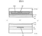
なお、図13は、図12に対応した図であり、ブラックマトリクスBMの近傍に位置づけられるカラーフィルタCFが該ブラックマトリクスBMをその全域にわたって被っている構成を示したものである。上述したと同様、シールド電極SEの透明基板SUB1までの電気的距離を拡大でき画素電極PXへの影響を低減させることができるようになるからである。 FIG. 13 is a diagram corresponding to FIG. 12, and shows a configuration in which the color filter CF positioned in the vicinity of the black matrix BM covers the entire black matrix BM. As described above, the electrical distance of the shield electrode SE to the transparent substrate SUB1 can be increased, and the influence on the pixel electrode PX can be reduced.
実施例3.
図14は、本発明による液晶表示装置の画素の構成の他の実施例を示す平面図で、図9と対応した図となっている。また、図14のD−D’線における断面図を図15に示している。
図9の場合と比較して異なる構成は、透明基板SUB2側に形成されるシールド電極SEをゲート信号線GLではなく、対向電圧信号線CLに対向するようにして形成した点にある。
Example 3
FIG. 14 is a plan view showing another embodiment of the pixel configuration of the liquid crystal display device according to the present invention and corresponds to FIG. Further, FIG. 15 shows a cross-sectional view taken along line DD ′ of FIG.
9 differs from the case of FIG. 9 in that the shield electrode SE formed on the transparent substrate SUB2 side is formed so as to face the counter voltage signal line CL, not the gate signal line GL.
また、この実施例の場合、ブラックマトリクスBMは画素領域の周辺を除く中央部に開口を設けたパターンとしていることは図9の場合と同じである。
このため、シールド電極SEは画素領域においてブラックマトリクスBMによって覆われていない構成となり、該シールド電極SEの画素領域の電界に対する影響(電界の擾乱)は、図9の場合と比較して大きくなることは免れない。
In the case of this embodiment, the black matrix BM has a pattern in which an opening is provided in the central portion excluding the periphery of the pixel region as in the case of FIG.
Therefore, the shield electrode SE is not covered with the black matrix BM in the pixel region, and the influence (electric field disturbance) of the shield electrode SE on the electric field in the pixel region is larger than that in the case of FIG. Is inevitable.
それ故、図15に示すように、シールド電極SEの幅をW1、対向電圧信号線CLの幅をW3、シールド電極SEの走行の方向に平行な各辺のうち一方側の辺から対向電圧信号線CLの同方向側の辺までの距離をL3、透明基板SUB2のブラックマトリクスBMが形成されていない領域における、カラーフィルタCF、平坦化膜OCおよび配向膜ALの積層体からなる厚さをd2とした場合、
[数1] W3>W1、かつL3>d2 …… (1)
の関係を満足するようにそれらの位置関係を規定している。これにより、シールド電極SEを電気的に遠く配置できたことになり、シールド電極SEの画素領域の電界への影響を抑制できる。
Therefore, as shown in FIG. 15, the width of the shield electrode SE is W1, the width of the counter voltage signal line CL is W3, and the counter voltage signal is output from one side of the sides parallel to the traveling direction of the shield electrode SE. The distance to the side in the same direction of the line CL is L3, and the thickness of the transparent substrate SUB2 in the region where the black matrix BM is not formed is the thickness of the laminate of the color filter CF, the planarization film OC, and the alignment film AL. If
[Equation 1] W3> W1 and L3> d2 (1)
The positional relationship is defined so as to satisfy the relationship. As a result, the shield electrode SE can be disposed far away electrically, and the influence of the shield electrode SE on the electric field in the pixel region can be suppressed.
また、他の実施例として、透明基板SUB1側において、対向電圧信号線CLを被う第2の絶縁膜GIから液晶表面の配向膜ALまでの積層体からなる厚さをd1とした場合、[数2] W3>W1、かつL3>(d2+d1) …… (2)
の関係を満足するようにそれらの位置関係を規定するようにしてもよい。このようにした場合、有効領域に対し、シールド電極SEを信号線より電気的に遠い位置に位置付けられるからである。
Also, if the As another example, the transparent substrate SUB1 side, the second insulating film GI thickness a laminate to the orientation film AL of the liquid crystal surface from of which covers the counter voltage signal line CL set to
These positional relationships may be defined so as to satisfy the relationship. This is because, in this case, the shield electrode SE can be positioned far from the signal line with respect to the effective region.
さらに、シールド電極と下層の信号線に関する上記(1)式で示す関係あるいは上記(2)式で示す関係は、ブラックマトリクス等の遮光層を有する領域に適用してもよいことはもちろんである。さらに効果の向上が図れるからである。 Further, it is needless to say that the relationship expressed by the above equation (1) or the relationship expressed by the above equation (2) regarding the shield electrode and the lower signal line may be applied to a region having a light shielding layer such as a black matrix. This is because the effect can be further improved.
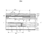
実施例4.
図16は、本発明による液晶表示装置の画素の他の実施例を示す平面図で、図14と対応した図となっている。また、図16のA−A’線における断面図を図17に、B−B’線における断面図を図18に示している。
Example 4
FIG. 16 is a plan view showing another embodiment of the pixel of the liquid crystal display device according to the present invention and corresponds to FIG. Further, a cross-sectional view taken along the line AA ′ in FIG. 16 is shown in FIG. 17, and a cross-sectional view taken along the line BB ′ is shown in FIG.
図16において、シールド電極SEはたとえばゲート信号線GLと対向するように形成したものであり、画素領域の構成において、画素電極PXと対向電極CTの構成が異なるのみで他は同様となっている。 In FIG. 16, the shield electrode SE is formed so as to face the gate signal line GL, for example, and the structure of the pixel region is the same except that the structure of the pixel electrode PX and the counter electrode CT is different. .
また、この場合、画素電極PXおよび対向電極CTは、そのいずれもがたとえばITO等の透光性の導電膜から構成されている。
すなわち、対向電極CTは第1の絶縁膜INSと第2の絶縁膜GIとの間に形成され、画素領域のほぼ全域に、この実施例の場合は図中x方向に隣接する他の画素領域の対向電極CTと互いに接続されて、形成されている。
In this case, each of the pixel electrode PX and the counter electrode CT is formed of a light-transmitting conductive film such as ITO.
In other words, the counter electrode CT is formed between the first insulating film INS and the second insulating film GI, and in the pixel region in the whole area, in this embodiment, another pixel region adjacent in the x direction. The counter electrodes CT are connected to each other.
また、画素電極PXは保護膜PASの上面に形成され、図中x方向に延在する電極がその延在方向と交差する方向に複数並設されてなす電極群によって形成されている。
なお、実施例に示す画素電極PXの各電極は、画素領域の中央をy方向に走行する仮想の線を境にし、その両脇における各電極が若干傾いて形成され、“へ”の字のパターンとなっている。いわゆるマルチドメイン方式を採用しているからである。
Further, the pixel electrode PX is formed on the upper surface of the protective film PAS, and is formed by an electrode group formed by arranging a plurality of electrodes extending in the x direction in the drawing in a direction intersecting the extending direction.
In addition, each electrode of the pixel electrode PX shown in the embodiment is formed by slightly tilting each electrode on both sides of a virtual line running in the y direction in the center of the pixel region. It is a pattern. This is because a so-called multi-domain method is adopted.
画素電極PXの各電極はその電極群の周辺にて枠体を有するパターンとすることにより互いに電気的に接続され、該枠体の一部において、保護膜PAS、第2の絶縁膜GI、第1の絶縁膜INSを貫通して形成したスルーホールを通して薄膜トランジスタTFTのソース電極に接続されている。 The electrodes of the pixel electrode PX are electrically connected to each other by forming a pattern having a frame around the electrode group. In a part of the frame, the protective film PAS, the second insulating film GI, the first It is connected to the source electrode of the thin film transistor TFT through a through hole formed through one insulating film INS.
このような構成からなる画素は、対向電極CTが隣接する画素領域のそれと接続され、それ自体が対向電圧信号線CLの機能をもたせることから、たとえば金属層で形成した対向電圧信号線CLが存在しないことから、シールド電極SEの配置個所としてゲート信号線GLと対向する個所を選択したものである。なお、この場合において、ドレイン信号線DLと対向するようにして形成してもよく、またゲート信号線GLおよびドレイン信号線DLに対向するようにして形成してもよい。 A pixel having such a configuration has a counter voltage signal line CL formed of, for example, a metal layer because the counter electrode CT is connected to that of the adjacent pixel region and has the function of the counter voltage signal line CL itself. For this reason, the portion facing the gate signal line GL is selected as the position where the shield electrode SE is disposed. In this case, it may be formed so as to face the drain signal line DL, or may be formed so as to face the gate signal line GL and the drain signal line DL.
上述した各実施例はそれぞれ単独に、あるいは組み合わせて用いても良い。それぞれの実施例での効果を単独であるいは相乗して奏することができるからである。 Each of the embodiments described above may be used alone or in combination. This is because the effects of the respective embodiments can be achieved independently or synergistically.
SUB…透明電極、GL…ゲート信号線、DL…ドレイン信号線、CL…対向電圧信号線、TFT…薄膜トランジスタ、PX…画素電極、CT…対向電極、GI…絶縁膜、PAS…保護膜、BM…ブラックマトリクス、FIL…カラーフィルタ、OC…平坦化膜、SE…シールド電極
SUB ... Transparent electrode, GL ... Gate signal line, DL ... Drain signal line, CL ... Counter voltage signal line, TFT ... Thin film transistor, PX ... Pixel electrode, CT ... Counter electrode, GI ... Insulating film, PAS ... Protective film, BM ... Black matrix, FIL ... color filter, OC ... flattening film, SE ... shield electrode
Claims (3)
前記第2の基板にブラックマトリクスと、該ブラックマトリクスより前記第2の基板側に形成された導電層を有し、
該導電層は、該導電層に対向する領域で前記第1の基板に形成された最上層の電極あるいは配線より幅が狭く形成され、
前記第1の基板にゲート信号線が形成され、該ゲート信号線より上層に絶縁膜を介して該ゲート信号線の幅よりも大きな幅を有する対向電圧信号線が形成され、前記対向電極は該対向電圧信号線と接続されて形成され、前記ブラックマトリクスから前記対向電圧信号線までの距離が、前記ブラックマトリクスから前記導電層までの距離よりも小さくなっていることを特徴とする液晶表示装置。 Of the first and second substrates disposed opposite to each other through the liquid crystal, the pixel electrode on the liquid crystal side of the first substrate has a counter electrode that generates an electric field between the pixel electrode and the pixel electrode,
A black matrix on the second substrate, and a conductive layer formed on the second substrate side from the black matrix;
The conductive layer is formed to be narrower than the uppermost electrode or wiring formed on the first substrate in a region facing the conductive layer ,
A gate signal line is formed on the first substrate, a counter voltage signal line having a width larger than the width of the gate signal line is formed above the gate signal line through an insulating film, and the counter electrode has the It is formed and is connected to the counter voltage signal line, the distance from the black matrix to the counter voltage signal line, a liquid crystal display you characterized in that is smaller than the distance from the black matrix to said conductive layer apparatus.
前記第2の基板にブラックマトリクスと、該ブラックマトリクスより前記第2の基板側に形成された導電層を有し、
該導電層は、該導電層に対向する領域で前記第1の基板に形成された最上層の電極あるいは配線より幅が狭く形成され、
前記ブラックマトリクスと前記第1の基板に形成された最上層の電極あるいは配線までの距離が、前記ブラックマトリクスから前記導電層までの距離よりも小さくなっていることを特徴とする液晶表示装置。 Of the first and second substrates disposed opposite to each other through the liquid crystal, the pixel electrode on the liquid crystal side of the first substrate has a counter electrode that generates an electric field between the pixel electrode and the pixel electrode,
A black matrix on the second substrate, and a conductive layer formed on the second substrate side from the black matrix;
The conductive layer is formed to be narrower than the uppermost electrode or wiring formed on the first substrate in a region facing the conductive layer ,
The distance to the electrode or wiring of the uppermost layer formed on the said black matrix first substrate, the liquid you characterized in that is smaller than the distance from the black matrix to said conductive layer crystal display device .
他方の基板に導電層を有し、
前記導電層が前記ゲート信号線延在方向に形成され、
前記ドレイン信号線の延在方向で、前記導電層間の距離が前記ゲート信号線間の距離より大きいことを特徴とする液晶表示装置。 Of each substrate arranged opposite to the liquid crystal, the pixel region on the liquid crystal side of one substrate has a plurality of gate signal lines and a plurality of drain signal lines, and is surrounded by adjacent gate signal lines and drain signal lines. A pixel electrode in a pixel region determined as a region, and a counter electrode that generates an electric field between the pixel electrode,
Having a conductive layer on the other substrate;
The conductive layer is formed in the gate signal line extending direction;
The liquid crystal display device, wherein a distance between the conductive layers is larger than a distance between the gate signal lines in the extending direction of the drain signal lines.
Priority Applications (1)
| Application Number | Priority Date | Filing Date | Title |
|---|---|---|---|
| JP2003394936A JP4381785B2 (en) | 2003-11-26 | 2003-11-26 | Liquid crystal display |
Applications Claiming Priority (1)
| Application Number | Priority Date | Filing Date | Title |
|---|---|---|---|
| JP2003394936A JP4381785B2 (en) | 2003-11-26 | 2003-11-26 | Liquid crystal display |
Publications (2)
| Publication Number | Publication Date |
|---|---|
| JP2005156899A JP2005156899A (en) | 2005-06-16 |
| JP4381785B2 true JP4381785B2 (en) | 2009-12-09 |
Family
ID=34720822
Family Applications (1)
| Application Number | Title | Priority Date | Filing Date |
|---|---|---|---|
| JP2003394936A Expired - Fee Related JP4381785B2 (en) | 2003-11-26 | 2003-11-26 | Liquid crystal display |
Country Status (1)
| Country | Link |
|---|---|
| JP (1) | JP4381785B2 (en) |
Families Citing this family (8)
| Publication number | Priority date | Publication date | Assignee | Title |
|---|---|---|---|---|
| JP4572854B2 (en) | 2006-03-29 | 2010-11-04 | ソニー株式会社 | Liquid crystal device and electronic device |
| TWI752316B (en) | 2006-05-16 | 2022-01-11 | 日商半導體能源研究所股份有限公司 | Liquid crystal display device |
| KR101395223B1 (en) | 2006-12-04 | 2014-05-16 | 삼성디스플레이 주식회사 | Liquid crystal display device |
| JP5333969B2 (en) * | 2009-09-15 | 2013-11-06 | 株式会社ジャパンディスプレイ | Liquid crystal devices and electronic equipment |
| JP6028345B2 (en) * | 2012-03-13 | 2016-11-16 | 大日本印刷株式会社 | Color filter forming substrate for horizontal electric field type LCD display panel and horizontal electric field type LCD display panel |
| JP5953120B2 (en) | 2012-05-25 | 2016-07-20 | 株式会社ジャパンディスプレイ | Liquid crystal display |
| JP6369801B2 (en) * | 2014-07-24 | 2018-08-08 | Tianma Japan株式会社 | Liquid crystal display |
| JP7344851B2 (en) * | 2018-11-28 | 2023-09-14 | 株式会社半導体エネルギー研究所 | liquid crystal display device |
-
2003
- 2003-11-26 JP JP2003394936A patent/JP4381785B2/en not_active Expired - Fee Related
Also Published As
| Publication number | Publication date |
|---|---|
| JP2005156899A (en) | 2005-06-16 |
Similar Documents
| Publication | Publication Date | Title |
|---|---|---|
| US7782426B2 (en) | Liquid crystal display device | |
| US9507230B2 (en) | Array substrate, liquid crystal panel and liquid crystal display | |
| JP4059676B2 (en) | Liquid crystal display | |
| JP5486784B2 (en) | Liquid crystal display | |
| US8284366B2 (en) | Liquid crystal display device | |
| US8035108B2 (en) | Thin film transistor substrate, liquid crystal display panel including the same, and method of manufacturing liquid crystal display panel | |
| KR101323412B1 (en) | Liquid crystal display device and manufacturing method of the same | |
| JP2009223245A (en) | Liquid crystal display device | |
| JP2005055897A (en) | Multi-domain liquid crystal display | |
| CN110196659B (en) | Display device with sensor | |
| JP2006091274A (en) | Liquid crystal display device | |
| US20230205020A1 (en) | Display device | |
| JP4381785B2 (en) | Liquid crystal display | |
| JP4731869B2 (en) | Thin film transistor display panel | |
| US9400409B2 (en) | Liquid crystal display | |
| US20090086135A1 (en) | Liquid Crystal Display Device | |
| KR101282402B1 (en) | Liquid crystal display device | |
| KR20120007323A (en) | Liquid crystal display device having high aperture ratio and fabricating method of the same | |
| US20130107184A1 (en) | Liquid crystal display | |
| CN112384849B (en) | Display device | |
| US11169424B2 (en) | Display device | |
| US11003031B2 (en) | Display apparatus | |
| KR20080087507A (en) | Liquid crystal display device and fabricating method thereof | |
| CN112384849A (en) | Display device | |
| JP2004109418A (en) | Liquid crystal display device |
Legal Events
| Date | Code | Title | Description |
|---|---|---|---|
| A621 | Written request for application examination |
Free format text: JAPANESE INTERMEDIATE CODE: A621 Effective date: 20060213 |
|
| A977 | Report on retrieval |
Free format text: JAPANESE INTERMEDIATE CODE: A971007 Effective date: 20090127 |
|
| A131 | Notification of reasons for refusal |
Free format text: JAPANESE INTERMEDIATE CODE: A131 Effective date: 20090303 |
|
| A521 | Request for written amendment filed |
Free format text: JAPANESE INTERMEDIATE CODE: A523 Effective date: 20090430 |
|
| TRDD | Decision of grant or rejection written | ||
| A01 | Written decision to grant a patent or to grant a registration (utility model) |
Free format text: JAPANESE INTERMEDIATE CODE: A01 Effective date: 20090915 |
|
| A01 | Written decision to grant a patent or to grant a registration (utility model) |
Free format text: JAPANESE INTERMEDIATE CODE: A01 |
|
| A61 | First payment of annual fees (during grant procedure) |
Free format text: JAPANESE INTERMEDIATE CODE: A61 Effective date: 20090916 |
|
| FPAY | Renewal fee payment (event date is renewal date of database) |
Free format text: PAYMENT UNTIL: 20121002 Year of fee payment: 3 |
|
| R150 | Certificate of patent or registration of utility model |
Ref document number: 4381785 Country of ref document: JP Free format text: JAPANESE INTERMEDIATE CODE: R150 Free format text: JAPANESE INTERMEDIATE CODE: R150 |
|
| S111 | Request for change of ownership or part of ownership |
Free format text: JAPANESE INTERMEDIATE CODE: R313121 Free format text: JAPANESE INTERMEDIATE CODE: R313115 |
|
| FPAY | Renewal fee payment (event date is renewal date of database) |
Free format text: PAYMENT UNTIL: 20121002 Year of fee payment: 3 |
|
| R350 | Written notification of registration of transfer |
Free format text: JAPANESE INTERMEDIATE CODE: R350 |
|
| FPAY | Renewal fee payment (event date is renewal date of database) |
Free format text: PAYMENT UNTIL: 20121002 Year of fee payment: 3 |
|
| FPAY | Renewal fee payment (event date is renewal date of database) |
Free format text: PAYMENT UNTIL: 20131002 Year of fee payment: 4 |
|
| R250 | Receipt of annual fees |
Free format text: JAPANESE INTERMEDIATE CODE: R250 |
|
| R250 | Receipt of annual fees |
Free format text: JAPANESE INTERMEDIATE CODE: R250 |
|
| R250 | Receipt of annual fees |
Free format text: JAPANESE INTERMEDIATE CODE: R250 |
|
| R250 | Receipt of annual fees |
Free format text: JAPANESE INTERMEDIATE CODE: R250 |
|
| R250 | Receipt of annual fees |
Free format text: JAPANESE INTERMEDIATE CODE: R250 |
|
| R250 | Receipt of annual fees |
Free format text: JAPANESE INTERMEDIATE CODE: R250 |
|
| R250 | Receipt of annual fees |
Free format text: JAPANESE INTERMEDIATE CODE: R250 |
|
| R250 | Receipt of annual fees |
Free format text: JAPANESE INTERMEDIATE CODE: R250 |
|
| R250 | Receipt of annual fees |
Free format text: JAPANESE INTERMEDIATE CODE: R250 |
|
| S531 | Written request for registration of change of domicile |
Free format text: JAPANESE INTERMEDIATE CODE: R313531 |
|
| S533 | Written request for registration of change of name |
Free format text: JAPANESE INTERMEDIATE CODE: R313533 |
|
| R350 | Written notification of registration of transfer |
Free format text: JAPANESE INTERMEDIATE CODE: R350 |
|
| LAPS | Cancellation because of no payment of annual fees |