JP4305811B2 - Liquid crystal display device, image display device and manufacturing method thereof - Google Patents
Liquid crystal display device, image display device and manufacturing method thereof Download PDFInfo
- Publication number
- JP4305811B2 JP4305811B2 JP2002244606A JP2002244606A JP4305811B2 JP 4305811 B2 JP4305811 B2 JP 4305811B2 JP 2002244606 A JP2002244606 A JP 2002244606A JP 2002244606 A JP2002244606 A JP 2002244606A JP 4305811 B2 JP4305811 B2 JP 4305811B2
- Authority
- JP
- Japan
- Prior art keywords
- layer
- pixel
- electrode
- liquid crystal
- insulating layer
- Prior art date
- Legal status (The legal status is an assumption and is not a legal conclusion. Google has not performed a legal analysis and makes no representation as to the accuracy of the status listed.)
- Expired - Lifetime
Links
Images


Classifications
-
- G—PHYSICS
- G02—OPTICS
- G02F—OPTICAL DEVICES OR ARRANGEMENTS FOR THE CONTROL OF LIGHT BY MODIFICATION OF THE OPTICAL PROPERTIES OF THE MEDIA OF THE ELEMENTS INVOLVED THEREIN; NON-LINEAR OPTICS; FREQUENCY-CHANGING OF LIGHT; OPTICAL LOGIC ELEMENTS; OPTICAL ANALOGUE/DIGITAL CONVERTERS
- G02F1/00—Devices or arrangements for the control of the intensity, colour, phase, polarisation or direction of light arriving from an independent light source, e.g. switching, gating or modulating; Non-linear optics
- G02F1/01—Devices or arrangements for the control of the intensity, colour, phase, polarisation or direction of light arriving from an independent light source, e.g. switching, gating or modulating; Non-linear optics for the control of the intensity, phase, polarisation or colour
- G02F1/13—Devices or arrangements for the control of the intensity, colour, phase, polarisation or direction of light arriving from an independent light source, e.g. switching, gating or modulating; Non-linear optics for the control of the intensity, phase, polarisation or colour based on liquid crystals, e.g. single liquid crystal display cells
- G02F1/133—Constructional arrangements; Operation of liquid crystal cells; Circuit arrangements
- G02F1/136—Liquid crystal cells structurally associated with a semi-conducting layer or substrate, e.g. cells forming part of an integrated circuit
-
- G—PHYSICS
- G02—OPTICS
- G02F—OPTICAL DEVICES OR ARRANGEMENTS FOR THE CONTROL OF LIGHT BY MODIFICATION OF THE OPTICAL PROPERTIES OF THE MEDIA OF THE ELEMENTS INVOLVED THEREIN; NON-LINEAR OPTICS; FREQUENCY-CHANGING OF LIGHT; OPTICAL LOGIC ELEMENTS; OPTICAL ANALOGUE/DIGITAL CONVERTERS
- G02F1/00—Devices or arrangements for the control of the intensity, colour, phase, polarisation or direction of light arriving from an independent light source, e.g. switching, gating or modulating; Non-linear optics
- G02F1/01—Devices or arrangements for the control of the intensity, colour, phase, polarisation or direction of light arriving from an independent light source, e.g. switching, gating or modulating; Non-linear optics for the control of the intensity, phase, polarisation or colour
- G02F1/13—Devices or arrangements for the control of the intensity, colour, phase, polarisation or direction of light arriving from an independent light source, e.g. switching, gating or modulating; Non-linear optics for the control of the intensity, phase, polarisation or colour based on liquid crystals, e.g. single liquid crystal display cells
- G02F1/133—Constructional arrangements; Operation of liquid crystal cells; Circuit arrangements
- G02F1/1333—Constructional arrangements; Manufacturing methods
- G02F1/1343—Electrodes
- G02F1/134309—Electrodes characterised by their geometrical arrangement
-
- G—PHYSICS
- G02—OPTICS
- G02F—OPTICAL DEVICES OR ARRANGEMENTS FOR THE CONTROL OF LIGHT BY MODIFICATION OF THE OPTICAL PROPERTIES OF THE MEDIA OF THE ELEMENTS INVOLVED THEREIN; NON-LINEAR OPTICS; FREQUENCY-CHANGING OF LIGHT; OPTICAL LOGIC ELEMENTS; OPTICAL ANALOGUE/DIGITAL CONVERTERS
- G02F1/00—Devices or arrangements for the control of the intensity, colour, phase, polarisation or direction of light arriving from an independent light source, e.g. switching, gating or modulating; Non-linear optics
- G02F1/01—Devices or arrangements for the control of the intensity, colour, phase, polarisation or direction of light arriving from an independent light source, e.g. switching, gating or modulating; Non-linear optics for the control of the intensity, phase, polarisation or colour
- G02F1/13—Devices or arrangements for the control of the intensity, colour, phase, polarisation or direction of light arriving from an independent light source, e.g. switching, gating or modulating; Non-linear optics for the control of the intensity, phase, polarisation or colour based on liquid crystals, e.g. single liquid crystal display cells
- G02F1/133—Constructional arrangements; Operation of liquid crystal cells; Circuit arrangements
- G02F1/1333—Constructional arrangements; Manufacturing methods
- G02F1/133345—Insulating layers
-
- G—PHYSICS
- G02—OPTICS
- G02F—OPTICAL DEVICES OR ARRANGEMENTS FOR THE CONTROL OF LIGHT BY MODIFICATION OF THE OPTICAL PROPERTIES OF THE MEDIA OF THE ELEMENTS INVOLVED THEREIN; NON-LINEAR OPTICS; FREQUENCY-CHANGING OF LIGHT; OPTICAL LOGIC ELEMENTS; OPTICAL ANALOGUE/DIGITAL CONVERTERS
- G02F1/00—Devices or arrangements for the control of the intensity, colour, phase, polarisation or direction of light arriving from an independent light source, e.g. switching, gating or modulating; Non-linear optics
- G02F1/01—Devices or arrangements for the control of the intensity, colour, phase, polarisation or direction of light arriving from an independent light source, e.g. switching, gating or modulating; Non-linear optics for the control of the intensity, phase, polarisation or colour
- G02F1/13—Devices or arrangements for the control of the intensity, colour, phase, polarisation or direction of light arriving from an independent light source, e.g. switching, gating or modulating; Non-linear optics for the control of the intensity, phase, polarisation or colour based on liquid crystals, e.g. single liquid crystal display cells
- G02F1/133—Constructional arrangements; Operation of liquid crystal cells; Circuit arrangements
- G02F1/1333—Constructional arrangements; Manufacturing methods
- G02F1/1343—Electrodes
- G02F1/13439—Electrodes characterised by their electrical, optical, physical properties; materials therefor; method of making
-
- G—PHYSICS
- G02—OPTICS
- G02F—OPTICAL DEVICES OR ARRANGEMENTS FOR THE CONTROL OF LIGHT BY MODIFICATION OF THE OPTICAL PROPERTIES OF THE MEDIA OF THE ELEMENTS INVOLVED THEREIN; NON-LINEAR OPTICS; FREQUENCY-CHANGING OF LIGHT; OPTICAL LOGIC ELEMENTS; OPTICAL ANALOGUE/DIGITAL CONVERTERS
- G02F1/00—Devices or arrangements for the control of the intensity, colour, phase, polarisation or direction of light arriving from an independent light source, e.g. switching, gating or modulating; Non-linear optics
- G02F1/01—Devices or arrangements for the control of the intensity, colour, phase, polarisation or direction of light arriving from an independent light source, e.g. switching, gating or modulating; Non-linear optics for the control of the intensity, phase, polarisation or colour
- G02F1/13—Devices or arrangements for the control of the intensity, colour, phase, polarisation or direction of light arriving from an independent light source, e.g. switching, gating or modulating; Non-linear optics for the control of the intensity, phase, polarisation or colour based on liquid crystals, e.g. single liquid crystal display cells
- G02F1/133—Constructional arrangements; Operation of liquid crystal cells; Circuit arrangements
- G02F1/136—Liquid crystal cells structurally associated with a semi-conducting layer or substrate, e.g. cells forming part of an integrated circuit
- G02F1/1362—Active matrix addressed cells
- G02F1/136213—Storage capacitors associated with the pixel electrode
-
- G—PHYSICS
- G02—OPTICS
- G02F—OPTICAL DEVICES OR ARRANGEMENTS FOR THE CONTROL OF LIGHT BY MODIFICATION OF THE OPTICAL PROPERTIES OF THE MEDIA OF THE ELEMENTS INVOLVED THEREIN; NON-LINEAR OPTICS; FREQUENCY-CHANGING OF LIGHT; OPTICAL LOGIC ELEMENTS; OPTICAL ANALOGUE/DIGITAL CONVERTERS
- G02F1/00—Devices or arrangements for the control of the intensity, colour, phase, polarisation or direction of light arriving from an independent light source, e.g. switching, gating or modulating; Non-linear optics
- G02F1/01—Devices or arrangements for the control of the intensity, colour, phase, polarisation or direction of light arriving from an independent light source, e.g. switching, gating or modulating; Non-linear optics for the control of the intensity, phase, polarisation or colour
- G02F1/13—Devices or arrangements for the control of the intensity, colour, phase, polarisation or direction of light arriving from an independent light source, e.g. switching, gating or modulating; Non-linear optics for the control of the intensity, phase, polarisation or colour based on liquid crystals, e.g. single liquid crystal display cells
- G02F1/133—Constructional arrangements; Operation of liquid crystal cells; Circuit arrangements
- G02F1/136—Liquid crystal cells structurally associated with a semi-conducting layer or substrate, e.g. cells forming part of an integrated circuit
- G02F1/1362—Active matrix addressed cells
- G02F1/136286—Wiring, e.g. gate line, drain line
-
- G—PHYSICS
- G02—OPTICS
- G02F—OPTICAL DEVICES OR ARRANGEMENTS FOR THE CONTROL OF LIGHT BY MODIFICATION OF THE OPTICAL PROPERTIES OF THE MEDIA OF THE ELEMENTS INVOLVED THEREIN; NON-LINEAR OPTICS; FREQUENCY-CHANGING OF LIGHT; OPTICAL LOGIC ELEMENTS; OPTICAL ANALOGUE/DIGITAL CONVERTERS
- G02F1/00—Devices or arrangements for the control of the intensity, colour, phase, polarisation or direction of light arriving from an independent light source, e.g. switching, gating or modulating; Non-linear optics
- G02F1/01—Devices or arrangements for the control of the intensity, colour, phase, polarisation or direction of light arriving from an independent light source, e.g. switching, gating or modulating; Non-linear optics for the control of the intensity, phase, polarisation or colour
- G02F1/13—Devices or arrangements for the control of the intensity, colour, phase, polarisation or direction of light arriving from an independent light source, e.g. switching, gating or modulating; Non-linear optics for the control of the intensity, phase, polarisation or colour based on liquid crystals, e.g. single liquid crystal display cells
- G02F1/133—Constructional arrangements; Operation of liquid crystal cells; Circuit arrangements
- G02F1/136—Liquid crystal cells structurally associated with a semi-conducting layer or substrate, e.g. cells forming part of an integrated circuit
- G02F1/1362—Active matrix addressed cells
- G02F1/1368—Active matrix addressed cells in which the switching element is a three-electrode device
-
- G—PHYSICS
- G02—OPTICS
- G02F—OPTICAL DEVICES OR ARRANGEMENTS FOR THE CONTROL OF LIGHT BY MODIFICATION OF THE OPTICAL PROPERTIES OF THE MEDIA OF THE ELEMENTS INVOLVED THEREIN; NON-LINEAR OPTICS; FREQUENCY-CHANGING OF LIGHT; OPTICAL LOGIC ELEMENTS; OPTICAL ANALOGUE/DIGITAL CONVERTERS
- G02F1/00—Devices or arrangements for the control of the intensity, colour, phase, polarisation or direction of light arriving from an independent light source, e.g. switching, gating or modulating; Non-linear optics
- G02F1/01—Devices or arrangements for the control of the intensity, colour, phase, polarisation or direction of light arriving from an independent light source, e.g. switching, gating or modulating; Non-linear optics for the control of the intensity, phase, polarisation or colour
- G02F1/13—Devices or arrangements for the control of the intensity, colour, phase, polarisation or direction of light arriving from an independent light source, e.g. switching, gating or modulating; Non-linear optics for the control of the intensity, phase, polarisation or colour based on liquid crystals, e.g. single liquid crystal display cells
-
- G—PHYSICS
- G02—OPTICS
- G02F—OPTICAL DEVICES OR ARRANGEMENTS FOR THE CONTROL OF LIGHT BY MODIFICATION OF THE OPTICAL PROPERTIES OF THE MEDIA OF THE ELEMENTS INVOLVED THEREIN; NON-LINEAR OPTICS; FREQUENCY-CHANGING OF LIGHT; OPTICAL LOGIC ELEMENTS; OPTICAL ANALOGUE/DIGITAL CONVERTERS
- G02F2201/00—Constructional arrangements not provided for in groups G02F1/00 - G02F7/00
- G02F2201/12—Constructional arrangements not provided for in groups G02F1/00 - G02F7/00 electrode
- G02F2201/123—Constructional arrangements not provided for in groups G02F1/00 - G02F7/00 electrode pixel
-
- G—PHYSICS
- G02—OPTICS
- G02F—OPTICAL DEVICES OR ARRANGEMENTS FOR THE CONTROL OF LIGHT BY MODIFICATION OF THE OPTICAL PROPERTIES OF THE MEDIA OF THE ELEMENTS INVOLVED THEREIN; NON-LINEAR OPTICS; FREQUENCY-CHANGING OF LIGHT; OPTICAL LOGIC ELEMENTS; OPTICAL ANALOGUE/DIGITAL CONVERTERS
- G02F2201/00—Constructional arrangements not provided for in groups G02F1/00 - G02F7/00
- G02F2201/40—Arrangements for improving the aperture ratio
Description
【0001】
【発明の属する技術分野】
本発明は、液晶表示装置に係り、特に画素の点灯を所定の時間維持するための保持容量とその給電抵抗を低減し、かつ開口率を向上したアクティブマトリクス型の液晶表示装置に関する。
【0002】
【従来の技術】
アクティブマトリクス型の液晶表示装置は、一般に一対の基板の対向間隔に液晶を挟持し、上記一対の基板の一方に形成した薄膜トランジスタ等に代表される多数のスイッチング素子で駆動される画素電極で画素を選択する方式を採用したものである。この種の液晶表示装置の一つの形式は、上記一対の基板の一方(第1の基板)に対向する他方の基板(第2の基板)にカラーフィルタや共通電極を形成し、あるいはカラーフィルタも第1の基板に形成した、所謂縦電界方式である。
【0003】
また、他の形式として、上記共通電極に相当する対向電極を上記第1の基板側に形成する、所謂IPS方式がある。この形式でも、カラーフィルタを第1の基板または第2の基板側に形成したのも既知である。
【0004】
縦電界方式の液晶表示装置は、上記第1の基板の内面に、第1の方向(通常は水平走査方向)に延在して互いに並設された複数のゲート線と、このゲート線と交差する第2の方向(通常、垂直走査方向)に延在し互いに並設された複数のドレイン線とを備える。そして、ゲート線とドレイン線の各交差部付近に薄膜トランジスタ等のスイッチング素子を備え、このスイッチング素子で駆動される画素電極を有している。
【0005】
この縦電界方式では、画素電極に対向して第2の基板には共通電極が形成されており、選択された画素電極との間に基板面と略直交する方向の電界を生成し、画素電極と共通電極との間に挟持された液晶の分子の配列を変更させることにより、画素の点灯を行う。
【0006】
一方、IPS方式の液晶表示装置は、上記第1の基板の内面に、縦電界方式と同様のゲート線とドレイン線、およびスイッチング素子を有し、かつ同一基板上に櫛形の画素電極を形成し、この画素電極と隣接して対向電極が形成されている。そして、選択された画素電極と対向電極との間に基板面と略平行な方向に電界を生成し、画素電極と対向電極との間にある液晶の分子の配向方向を変化させることにより、画素の点灯を行うものである。さらに、この方式を発展させたものとして、対向電極をべた電極として、その上層あるいは下層に櫛形の画素電極を形成したものもある。
【0007】
上記した何れの形式の液晶表示装置においても、選択により点灯した画素の点灯時間を所定値に保持するための電荷の蓄積容量(以下、単に保持容量と言う)は画素電極とゲート線の重畳領域、あるいは画素電極の形成領域を横断するように形成した他の電極線と当該画素電極との重畳領域に形成され、この保持容量に電荷を蓄積するための給電路はゲート線あるいは上記他の電極線としている。
【0008】
【発明が解決しようとする課題】
このように、保持容量を形成する一方の電極は線状電極であり、その給電は一方向(当該電極の延在方向)であるため、給電抵抗が大きく、また給電端から遠ざかるに従って電圧降下が著しくなり、必要とする電荷を給電できなくなる場合がある。また、上記のゲート線は通常はドレイン線と交差しているため、その交差容量が増大する。その結果、液晶表示装置の高速駆動が困難となる一つの要因となっていた。これの対策として上記の他の電極線を用いたものがある。しかし、画素電極の形成領域に保持容量を形成すると、当然のこととして開口率が低下する。
【0009】
また高精細化に伴い1画素当たりの画素のサイズが縮小し、十分な保持容量を形成することが困難となってきているという課題がある。
【0010】
さらに、開口率を向上するには保持容量のサイズを小さくすることが有効であるが、これは保持容量の減少を招く。すなわち開口率向上と保持容量確保はトレードオフの関係にあるという課題がある。
【0011】
本発明の利点は、保持容量を構成する給電電極の抵抗を低減することにある。また画素の開口率の低下を回避して高輝度、かつ高速駆動のアクティブマトリクス型液晶表示装置を提供することにある。さらに、保持容量と開口率の両立を実現することにある。
【0012】
本発明のその他の利点は、以下の説明で明らかとなる。
【0013】
【課題を解決するための手段】
上記目的を達成するために、本発明の典型的な構成は、液晶表示装置のスイッチング素子形成基板の下層の少なくとも画素電極形成領域の大部分あるいは全域を占めるような広い面積の透明導電層(基準電極層)を形成し、その上層に絶縁層を介してスイッチング素子やその他の電極および配線を形成した構成とした。この構成により、保持容量に対する給電抵抗が大幅に低減される。また、開口率向上と保持容量増大のトレードオフを解消できる。以下、本発明の他の定評的な構成を記述する。
【0014】
(1):第1の基板と第2の基板の対向間隙に液晶を挟持し、前記第1の基板の内面に、第1の方向に延在し互いに並設された複数のゲート線および前記ゲート線と交差する第2の方向に延在し互いに並設された複数のドレイン線と、前記ゲート線とドレイン線の交差部に設けられた複数のスイッチング素子と、前記アクティブ素子で駆動される画素電極を少なくとも有し、前記複数の画素電極で画素領域が構成される液晶表示装置であって、
前記第1の基板の前記画素領域を含んで前記ゲート線、ドレイン線、スイッチング素子、画素電極を形成する電極形成層と前記第1の基板側との間に当該電極形成層に対して第1の絶縁層で絶縁した基準電極層を有し、
前記画素電極と前記基準電極層の間に画素の保持容量を形成する。
【0015】
この構成により、蓄積容量に対する給電抵抗が大幅に低減され、画素の開口率と保持容量の両立を実現した液晶表示装置を得ることができる。
【0016】
(2):(1)において、前記電極形成層は、前記第1の絶縁層の上層にゲート線、ゲート絶縁層、半導体層、ドレイン線、パッシベーション層、画素電極をこの順で有し、
前記画素電極と前記基準電極層の間に画素の保持容量を形成する。
【0017】
画素電極と基準電極層の間に形成されるパッシベーション層、ゲート絶縁層、第1の絶縁層で保持容量が形成されるため、液晶層からみた基準電極層までの距離を大幅に離間させることが可能となり、液晶の駆動用電界への基準電極層の電界の影響が軽減される。
【0018】
(3):(1)において、前記基準電極層が前記ゲート線と平行、かつ前記画素電極の形成領域に重畳して前記ゲート線の延在方向に有する。
【0019】
この構成により、ゲート線と基準電極層の間の寄生容量が低減され、また電位の安定化を図ることができる。
【0020】
(4):(1)において、前記基準電極層が前記第1の基板の前記ゲート線と前記ドレイン線および前記画素電極の形成領域を含む領域に有する。
【0021】
この構成により、基準電極層が、所謂べた電極であることで給電抵抗がさらに低減され、かつ給電方向の制限が無くなる。
【0022】
(5):(1)において、前記ゲート絶縁層より上層に前記パッシベーション層を有し、該パッシベーション層より上層に前記画素電極を有し、
前記画素電極の全部または一部が前記パッシベーション層を貫通して前記ゲート絶縁層に接している。
【0023】
この構成により、導電層と画素電極との間に形成される保持容量を画素電極がパッシベーション層を貫通する面積で調整できる。
【0024】
(6):(1)において、前記ゲート絶縁層より上層に前記パッシベーション層を有し、該パッシベーション層より上層に前記画素電極を有し、
前記画素領域における前記画素電極の全部または一部が前記パッシベーション層とゲート絶縁層とを貫通して前記第1の絶縁層に接している。
【0025】
この構成により、基準電極層と画素電極との間に形成される保持容量を画素電極がパッシベーション層とゲート絶縁層とを貫通する面積で調整できる。
【0026】
(7):(1)において、前記ゲート絶縁層より上層に前記パッシベーション層を有し、該パッシベーション層より上層に前記画素電極を有し、前記スイッチング素子は、前記ゲート絶縁層の上に前記パッシベーション層に形成したスルーホールを介して画素電極と接続するソース電極を有し、前記ソース電極の一部に前記ゲート線または前記ドレイン線に沿った延長部を有する。
【0027】
この構成により、ソース電極の延長部の長さ、または幅、すなわちソース電極が画素電極と重畳する面積を変えることで保持容量を調整できる。
【0028】
(8):(1)において、前記第1の絶縁層が有機絶縁層である。
【0029】
この構成により、前記基準電極層と前記電極形成層の間の電気的距離を向き絶縁層の場合より離間できる。そして基準電極層と前記ゲート線およびドレイン線との寄生容量を低減できる。
【0030】
(9):(1)において、前記ドレイン線の延在方向近傍と前記画素電極の間を遮光する遮光層を有する。
【0031】
この構成により、光漏れを防止できる。
【0032】
(10):(1)において、前記第2の基板の内面に、前記画素電極との間で画素を構成する共通電極を有する。
【0033】
(11):第1の基板と第2の基板の対向間隙に液晶を挟持し、前記第1の基板の内面に、第1の方向に延在し互いに並設された複数のゲート線および前記ゲート線と交差する第2の方向に延在し互いに並設された複数のドレイン線と、前記ゲート線とドレイン線の交差部に設けられた複数のスイッチング素子と、前記アクティブ素子で駆動される画素電極を少なくとも有し、前記複数の画素電極で画素領域が構成される液晶表示装置であって、
前記第1の基板の前記画素領域を含んで前記ゲート線、ドレイン線、スイッチング素子、画素電極を形成する電極形成層と前記第1の基板側との間に当該電極形成層に対して第1の絶縁層で絶縁した基準電極層を有し、
前記画素形成層は、前記第1の絶縁層の上層にゲート絶縁層、パッシベーション層、第2の有機絶縁層、画素電極をこの順で有し、
前記画素電極と前記基準電極層で画素の保持容量を形成する。
【0034】
この構成により、画素の開口率が向上し、導電層の面積が大きいために給電抵抗が低減できると共に、画素電極と基準電極層の間に形成されるパッシベーション層、ゲート絶縁層、第1の絶縁層で保持容量が形成されるため、当該保持容量の制御が容易になる。さらに、スイッチング素子の上層にも有機絶縁層を設けたことで、画素電極とドレイン線の重畳が可能となり、さらに開口率が向上する。画素電極とドレイン線を重畳した場合に、ドレイン線の延在方向近傍と画素電極の間の遮光層を省略できるため、またさらに開口率が向上する。
【0035】
(12):(11)において、前記基準電極層が前記ゲート線と平行、かつ前記画素電極の形成領域に重畳して前記ゲート線の延在方向に有する。
【0036】
この構成により、ゲート線と基準電極層の間の容量が低減され、保持容量の増大を抑制することができ、また電位の安定化を図ることができる。
【0037】
(13):(11)において、前記基準電極層が前記第1の基板の前記ゲート線と前記ドレイン線および前記画素電極の形成領域を含む領域に有する。
【0038】
この構成により、基準電極層が、所謂べた電極であることで給電抵抗がさらに低減され、かつ給電方向の制限が無くなる。
【0039】
(14):(11)において、前記第1の有機絶縁層がカラーフィルタである。
【0040】
この構成により、画素の開口率が向上し、導電層の面積が大きいために給電抵抗が低減できると共に、画素電極と基準電極層の間に形成されるパッシベーション層、ゲート絶縁層、有機材料である誘電率の小さいカラーフィルタ層で保持容量が形成されるため配線間寄生容量の増大を抑制できる。また、第1の基板にカラーフィルタ層を形成するため、第2の基板との位置合わせ裕度が大きくなる。
【0041】
(15)、(14)において、前記基準電極層が前記ゲート線と平行、かつ前記画素電極の形成領域に重畳して前記ゲート線の延在方向に有する。
【0042】
この構成により、ゲート線と導電層の間の容量が低減され、また電位の安定化を図ることができる。
【0043】
(16):(14)において、前記基準電極層が前記第1の基板の前記ゲート線と前記ドレイン線および前記画素電極の形成領域を含む領域に有する。
【0044】
この構成により、基準電極層が、所謂べた電極であることで給電抵抗がさらに低減され、かつ給電方向の制限が無くなる。
【0045】
(17):(11)において、前記第1の絶縁層が有機絶縁層である。
【0046】
この構成により、前記基準電極層と前記電極形成層の間の電気的距離を向き絶縁層の場合より離間できる。そして基準電極層と前記ゲート線およびドレイン線との寄生容量を低減できる。
【0047】
(18):(11)において、前記ドレイン線の延在方向近傍と前記画素電極の間を遮光する遮光層を有する。
【0048】
この構成により、光漏れを防止できる。
【0049】
(19):(11)において、前記第2の基板の内面に、前記画素電極との間で画素を構成する共通電極を有する。
【0050】
(20):第1の基板と第2の基板の対向間隙に液晶を挟持し、前記第1の基板の内面に、第1の方向に延在し互いに並設された複数のゲート線および前記ゲート線と交差する第2の方向に延在し互いに並設された複数のドレイン線と、前記ゲート線とドレイン線の交差部に設けられた複数のスイッチング素子と、前記アクティブ素子で駆動される画素電極を少なくとも有し、前記複数の画素電極で画素領域が構成される液晶表示装置であって、
前記第1の基板の前記画素領域を含んで前記ゲート線、ドレイン線、スイッチング素子、画素電極を形成する電極形成層と前記第1の基板側との間に当該電極形成層に対して第1の絶縁層で絶縁した基準電極層を有し、
前記画素形成層は、前記第1の絶縁層の上層にゲート絶縁層、パッシベーション層、画素電極をこの順で有し、かつ前記第1の絶縁層より上層で前記画素電極と接続した容量電極層を有し、
前記画素電極と前記基準電極層および前記容量電極層で画素の保持容量を形成する。
【0051】
この構成により、画素の開口率が向上し、導電層の面積が大きいために給電抵抗が低減できる。さらに容量電極層の面積、形状で保持容量を調整できるため、開口率と保持容量の両立が容易になる。さらに、パッシベーション層と画素電極の間に有機絶縁層を設けた場合には、画素電極とドレイン線の重畳が可能となり、さらに開口率が向上する。画素電極とドレイン線を重畳した場合に、ドレイン線の延在方向近傍と画素電極の間の遮光層を省略できるため、またさらに開口率が向上する。
【0052】
(21):(20)において、前記基準電極層が前記ゲート線と平行、かつ前記画素電極の形成領域に重畳して前記ゲート線の延在方向に有する。
【0053】
この構成により、ゲート線と基準電極層の間の容量が低減され、電位の安定化を図ることができる。
【0054】
(22):(20)において、前記基準電極層が前記第1の基板の前記ゲート線と前記ドレイン線および前記画素電極の形成領域を含む領域に有する。
【0055】
この構成により、基準電極層が、所謂べた電極であることで給電抵抗がさらに低減され、かつ給電方向の制限が無くなる。
【0056】
(23):(20)において、前記スイッチング素子は、前記ゲート絶縁層の上に前記パッシベーション層に形成したスルーホールを介して前記画素電極と接続するソース電極を有し、前記容量電極層は前記ソース電極に接続して前記画素電極の領域に有する。
【0057】
この構成により、前記容量電極層の大きさを変えることで保持容量を調整できる。
【0058】
(24):(20)において、前記第1の絶縁層がカラーフィルタである。
【0059】
この構成により、画素の開口率が向上し、導電層の面積が大きいために給電抵抗が低減できる。また、第1の基板にカラーフィルタ層を形成するため、第2の基板との位置合わせ裕度が大きくなる。
【0060】
(25):(20)において、前記容量電極層をパッシベーション層上に有し、パッシベーション層上に有機絶縁層を有し、前記画素電極は前記有機絶縁層上に形成され、前記画素電極は前記有機絶縁層に形成したスルーホールを介して前記容量電極層に接続した。
【0061】
この構成により、前記容量電極層の大きさを変えることで保持容量を調整できる。
【0062】
(26):(20)において、前記容量電極層をゲート絶縁層上に有し、前記画素電極を前記パッシベーション層に形成したスルーホールを介して前記容量電極層に接続した。
【0063】
この構成により、前記容量電極層の大きさを変えることで保持容量を調整できる。
【0064】
(27):(20)において、前記容量電極層を前記第1の絶縁層上に有し、前記画素電極を前記パッシベーション層を貫通し前記ゲート絶縁層に形成したスルーホールを介して前記容量電極層に接続した。
【0065】
この構成により、導電層と画素電極との間に形成される保持容量を画素電極がパッシベーション層とゲート絶縁層とを貫通する面積で調整できる。
【0066】
(28):(20)において、前記第1の絶縁層が有機絶縁層である。
【0067】
この構成により、前記基準電極層と前記電極形成層の間の電気的距離を向き絶縁層の場合より離間できる。そして基準電極層と前記ゲート線およびドレイン線との寄生容量を低減できる。
【0068】
(29):(20)において、前記ドレイン線の延在方向近傍と前記画素電極の間を遮光する遮光層を有する。
【0069】
この構成により、光漏れを防止できる。
【0070】
(30):(20)において、前記第2の基板の内面に、前記画素電極との間で画素を構成する共通電極を有する。
【0071】
(31):第1の基板と第2の基板の対向間隙に液晶を挟持し、前記第1の基板の内面に、第1の方向に延在し互いに並設された複数のゲート線および前記ゲート線と交差する第2の方向に延在し互いに並設された複数のドレイン線と、前記ゲート線とドレイン線の交差部に設けられた複数のスイッチング素子と、前記アクティブ素子で駆動される画素電極を少なくとも有し、前記複数の画素電極で画素領域が構成される液晶表示装置であって、
前記第1の基板の前記画素領域を含んで前記ゲート線、ドレイン線、スイッチング素子、画素電極を形成する電極形成層と前記第1の基板側との間に当該電極形成層に対して第1の絶縁層で絶縁した基準電極層を有し、
前記電極形成層は、前記第1の絶縁層の上層にゲート絶縁層、パッシベーション層、画素電極をこの順で有し、かつ前記第1の絶縁層と前記パッシベーション層の間に前記画素電極と接続した容量電極層を有し、
前記画素電極と前記基準電極層および前記容量電極層で画素の保持容量を形成する。
【0072】
この構成により、画素の開口率が向上し、基準電極層の面積が大きいために給電抵抗が低減、かつ容量電極層の面積、形状で保持容量を調整できる。
【0073】
(32):(31)において、前記基準電極層が前記ゲート線と平行、かつ前記画素電極の形成領域に重畳して前記ゲート線の延在方向に有する。
【0074】
この構成により、ゲート線と基準電極層の間の容量が低減され、配線間寄生容量の増大を抑制することができ、また電位の安定化を図ることができる。
【0075】
(33):(31)において、前記基準電極層が前記第1の基板の前記ゲート線と前記ドレイン線および前記画素電極の形成領域を含む領域に有する。
【0076】
この構成により、基準電極層が所謂べた電極であることで給電抵抗がさらに低減され、かつ給電方向の制限が無くなる。
【0077】
(34):(31)において、前記有機絶縁層がカラーフィルタである。
【0078】
この構成により、画素の開口率が向上し、基準電極層の面積が大きいために給電抵抗が低減できると共に、カラーフィルタが有機膜であることにより配線間寄生容量が低減できる。また、第1の基板にカラーフィルタ層を形成するため、第2の基板との位置合わせ裕度が大きくなる。
【0079】
(35):(31)において、前記第1の絶縁層が有機絶縁層である。
【0080】
この構成により、前記基準電極層と前記電極形成層の間の電気的距離を向き絶縁層の場合より離間できる。そして基準電極層と前記ゲート線およびドレイン線との寄生容量を低減できる。
【0081】
(36):(31)において、前記ドレイン線の延在方向近傍と前記画素電極の間を遮光する遮光層を有する。
【0082】
この構成により、光漏れを防止できる。
【0083】
(37):(31)において、前記容量電極層を前記第1の絶縁層上に有し、前記容量電極層を前記第1の絶縁層を貫通したスルーホールを介して前記基準電極層に接続した。
【0084】
この構成により、基準電極層と画素電極との間に形成される保持容量を基準電極層に接続した容量電極層の面積で調整できる。
【0085】
(38):(31)において、前記容量電極層をゲート絶縁層上に有し、前記容量電極層を前記ゲート絶縁層を貫通したスルーホールを介して前記基準電極層に接続した。
【0086】
この構成により、基準電極層と画素電極との間に形成される保持容量を基準電極層に接続した容量電極層の面積で調整できる。
【0087】
(39):(31)において、前記容量電極層を前記パッシベーション層上に有し、前記容量電極層を前記パッシベーション層と前記ゲート絶縁層および前記第1の絶縁層を貫通したスルーホールを介して前記容量電極層に接続した。
【0088】
この構成により、基準電極層と画素電極との間に形成される保持容量を基準電極層に接続した容量電極層の面積で調整できる。
【0089】
(40):(31)において、さらに前記容量電極層をゲート絶縁層上に有すると共に、前記第1の絶縁層上に第2の容量電極層を有し、前記画素電極をパッシベーション層に形成したスルーホールを介して前記容量電極層に接続すると共に、前記第2の容量電極層を前記第1の絶縁層に形成したスルーホールを介して前記基準電極層に接続した。
【0090】
この構成により、保持容量は容量電極層と第2の容量電極層との面積で容易に調整できる。また保持容量をさらに増大することが出来る。
【0091】
(41):(31)において、前記第1の絶縁層が有機絶縁層である。
【0092】
この構成により、前記基準電極層と前記電極形成層の間の電気的距離を向き絶縁層の場合より離間できる。そして基準電極層と前記ゲート線およびドレイン線との寄生容量を低減できる。
【0093】
(42):(31)において、前記ドレイン線の延在方向近傍と前記画素電極の間を遮光する遮光層を有する。
【0094】
この構成により、光漏れを防止できる。
【0095】
(43):(31)において、前記第2の基板の内面に、前記画素電極との間で画素を構成する共通電極を有する。
【0096】
(44):第1の基板と第2の基板の対向間隙に液晶を挟持し、前記第1の基板の内面に、第1の方向に延在し互いに並設された複数のゲート線および前記ゲート線と交差する第2の方向に延在し互いに並設された複数のドレイン線と、前記ゲート線とドレイン線の交差部に設けられた複数のスイッチング素子と、前記アクティブ素子で駆動される画素電極と前記画素電極との間で画素駆動用の電界を生成する対向電極とを少なくとも有し、前記複数の画素電極で画素領域が構成される液晶表示装置であって、
前記第1の基板の前記画素領域を含んで前記ゲート線、ドレイン線、スイッチング素子、画素電極を形成する電極形成層と前記第1の基板側との間に当該電極形成層に対して第1の絶縁層で絶縁した基準電極層を有し、
前記画素電極と前記基準電極層の間に画素の保持容量を形成する。
【0097】
この構成により、開口率と保持容量の両立が実現するする。また保持容量を形成するための画素電極や配線の面積を大きくする必要がないため開口率が向上する。また、基準電極層の面積が大きいために給電抵抗が低減できる。
【0098】
(45):(44)において、前記対向電極を前記有機絶縁層上に有し、前記対向電極が前記第1の絶縁層に形成したスルーホールを介して前記基準電極層に接続されている。
【0099】
この構成により、基準電極層の面積が大きいために対向電極への給電抵抗が低減できる。
【0100】
(46):(44)において、前記対向電極を前記ゲート絶縁層上に有し、前記対向電極が前記ゲート絶縁層と前記第1の絶縁層に形成したスルーホールを介して前記基準電極層に接続されている。
【0101】
この構成により、基準電極層の面積が大きいために給電抵抗が低減できる。
【0102】
(47):(44)において、前記対向電極を前記パッシベーション層上に有し、前記対向電極が前記パッシベーション層と前記ゲート絶縁層および前記第1の絶縁層に形成したスルーホールを介して前記基準電極層に接続されている。
【0103】
この構成により、基準電極層の面積が大きいために給電抵抗が低減できる。
【0104】
(48):(44)において、前記基準電極層が前記ゲート線と平行、かつ前記画素電極の形成領域に重畳して前記ゲート線の延在方向に有する。
【0105】
この構成により、ゲート線と基準電極層の間の寄生容量が低減され、また電位の安定化を図ることができる。
【0106】
(49):(44)において、前記基準電極層が前記第1の基板の前記ゲート線と前記ドレイン線および前記画素電極の形成領域を含む領域に有する。
【0107】
この構成により、基準電極層が、所謂べた電極であることで給電抵抗がさらに低減され、かつ給電方向の制限が無くなる。
【0108】
(50):(44)において、前記対向電極は第1の絶縁層上に有すると共に、
ドレイン線と交差して隣接画素領域に延在し、当該隣接画素領域の基準電極層に前記第1の絶縁層に形成したスルーホールを介して接続されている。
【0109】
この構成により、仮にスルーホールの形成が不十分であっても隣接画素側から対向電極を通して給電がなされる。また、各対向電極と各基準電極とを接続するスルーホールを各画素毎に複数形成する場合には、当該電極層間の接続の信頼性を向上できる。
【0110】
(51):(44)において、前記対向電極は有機絶縁層上に有し、前記ゲート絶縁層上でドレイン線と交差して隣接画素領域に延在する導電層を有し、前記対向電極は前記ゲート絶縁層に形成したスルーホールを介して前記導電層に接続し、かつ前記導電層は前記第1の絶縁層に形成したスルーホールを介して前記基準電極層に接続されている。
【0111】
この構成により、仮にスルーホールの形成が不十分であっても隣接画素側から導電層を通して給電がなされる。また、各対向電極と各基準電極とを接続するスルーホールを各画素毎に複数形成することで、当該電極層間の接続の信頼性を向上できる。
【0112】
(52):(44)において、前記対向電極はパッシベーション層上に有し、前記ゲート絶縁層上でドレイン線と交差して隣接画素領域に延在する導電層を有し、前記対向電極は前記パッシベーション層と前記ゲート絶縁層に形成したスルーホールを介して前記導電層に接続し、かつ前記導電層は前記第1の絶縁層に形成したスルーホールを介して前記基準電極層に接続される。
【0113】
(53):(44)において、前記第1の絶縁層の下層に有する前記基準電極と前記第1の基板の間にカラーフィルタ層を有する。
【0114】
この構成により、カラーフィルタ層は前記基準電極で液晶層と隔離されるため、カラーフィルタ層の構成材料による液晶の汚染が阻止される。
【0115】
(54):(44)において、前記対向電極は前記第1の絶縁層上に前記ゲート線の延在方向と平行で、かつ画素領域にわたって形成され、各画素領域における前記基準電極に前記第1の絶縁層に形成したスルーホールを介して接続する。
【0116】
この構成により、保持容量は対向電極と画素電極の重畳部分で形成され、ゲート絶縁層は保持容量の誘電体となり、保持容量を増大させる場合に好適である。
【0117】
(55):(44)において、前記対向電極を各画素領域における前記基準電極に前記第1の絶縁層と前記ゲート絶縁層とを貫通して形成したスルーホールを介して接続し、前記対向電極と前記画素電極の重畳部分で保持容量を形成する。
【0118】
(56):(44)において、前記画素電極は前記ゲート絶縁層上に有し、前記対向電極は前記ゲート絶縁層下に有し、前記対向電極は前記第1の絶縁層に形成したスルーホールを介して前記基準電極に接続し、前記対向電極と前記画素電極とで保持容量を形成する。
【0119】
(57):(44)において、前記画素電極は前記対向電極と同層である。
【0120】
(58):(44)において、前記対向電極は前記画素電極より上層に配置され、ゲート絶縁膜と第1の絶縁膜に形成されたスルーホールを介して前記基準電極に接続している。
【0121】
(59):(44)において、前記第1の絶縁層が有機絶縁層である。
【0122】
(60):第1の基板と第2の基板の対向間隙に液晶を挟持し、前記第1の基板の内面に、第1の方向に延在し互いに並設された複数のゲート線および前記ゲート線と交差する第2の方向に延在し互いに並設された複数のドレイン線と、前記ゲート線とドレイン線の交差部に設けられた複数のスイッチング素子とを少なくとも有し、前記複数の画素電極で画素領域が構成される液晶表示装置であって、
前記第1の基板の前記画素領域を含んで前記ゲート線、ドレイン線、スイッチング素子、画素電極を形成する電極形成層と前記第1の基板側との間に当該電極形成層に対して第1の絶縁層で絶縁して前記画素領域の全域に重畳して基準電極を兼用する対向電極層を有し、
前記画素電極と前記対向電極層の間に画素の保持容量を形成する。
【0123】
この構造により、保持容量に対する給電抵抗が大幅に低減され、画質が向上する。また開口率と保持容量の両立が実現する。
【0124】
(61):(60)において、前記対向電極層が前記ゲート線と平行、かつ前記画素電極の形成領域に重畳して前記ゲート線の延在方向に有する。
【0125】
この構成により、独立した基準電極層を要せず、ゲート線と導電層の間の寄生容量が低減され、また電位の安定化を図ることができる。
【0126】
(62):(60)において、前記対向電極層が前記第1の基板の前記ゲート線と前記ドレイン線および前記画素電極の形成領域を含む領域に有する。
【0127】
この構成により、対向電極層が、所謂べた電極であることで給電抵抗がさらに低減され、かつ給電方向の制限が無くなる。
【0128】
(63):(60)において、前記画素電極の下層の絶縁層の層構成の全部または一部、および領域の全部または一部を除去した。
【0129】
この構成により、画素電極と対向電極との間に生成される電界強度が増大し、駆動電圧を低減することができる。
【0130】
(64):(60)において、前記対向電極層上に前記ゲート線の延在方向と平行に当該対向電極を隣接する対向電極に接続する接続線を有する。
【0131】
(65):(60)において、前記対向電極層下に前記ゲート線の延在方向と平行に当該対向電極を隣接する対向電極に接続する接続線を有する。
【0132】
上記(64)または(65)の構成により、仮にスルーホールの形成が不十分であっても隣接画素側から接続線を通して給電がなされる。また、各対向電極と各基準電極とを接続するスルーホールを各画素毎に複数形成する場合には、当該電極層間の接続の信頼性を向上できる。
【0133】
(66):(60)において、前記第1の絶縁層は前記画素領域内の一部で除去されている。
【0134】
本構成により、画素領域内に駆動電圧の異なる複数の領域を形成でき、マルチドメイン効果を得ることができる。
【0135】
(67):(60)において、前記第1の絶縁層の下層に有する前記基準電極と前記第1の基板の間にカラーフィルタ層を有する。
【0136】
(68):(60)において、前記第1の絶縁層が有機絶縁層である。
【0137】
(69):(68)において、前記有機絶縁層がカラーフィルタである。
【0138】
(70):第1の基板と第2の基板の対向間隙に液晶を挟持し、前記第1の基板の内面に、第1の方向に延在し互いに並設された複数のゲート線および前記ゲート線と交差する第2の方向に延在し互いに並設された複数のドレイン線と、前記ゲート線とドレイン線の交差部に設けられた複数のスイッチング素子と、前記アクティブ素子で駆動される画素電極と前記画素電極との間で画素駆動用の電界を生成する対向電極とを少なくとも有し、前記複数の画素電極で画素領域が構成される液晶表示装置であって、
前記第1の基板の前記画素領域を含んで前記ゲート線、ドレイン線、スイッチング素子、画素電極を形成する電極形成層と前記第1の基板側との間に当該電極形成層に対して第1の絶縁層で絶縁した基準電極層を有し、
前記電極形成層は、前記第1の絶縁層の上層にゲート絶縁層、パッシベーション層、有機絶縁層、対向電極をこの順で積層してなり、
前記対向電極層は、前記画素領域の前記ゲート線の延在方向に隣接する画素領域および前記ドレイン線の延在方向に隣接する画素領域にわたって共有され、
かつ前記対向電極層は、前記有機絶縁層、パッシベーション層、ゲート絶縁層、第1の絶縁層を電気的に貫通するスルーホールを介して前記基準電極層に接続し、
前記画素電極と前記基準電極層の間に画素の保持容量を形成する。
【0139】
この構成により、開口率が向上する。また、基準電極層の面積が極めて大きいために給電抵抗を大幅に低減できる。
【0140】
(71):(70)において、前記画素電極の下層であり、前記第1の絶縁層と前記ゲート絶縁層の間に形成された容量電極層を有し、該容量電極層は前記基準電極層とスルーホールを介して接続されている。
【0141】
この構成により、保持容量を容量電極層で増加させ、調整することができる。
【0142】
(72):(70)において、前記画素電極下の前記第1の絶縁層に除去領域を設けた。
【0143】
この構成により、画素電極と基準電極層の間に形成される保持容量を増大させることができる。
【0144】
(73):(70)において、前記第1の絶縁層が有機絶縁層である。
【0145】
(74):(73)において、前記有機絶縁層がカラーフィルタである。
【0146】
(75):第1の基板の内面に、第1の方向に延在し互いに並設された複数のゲート線および前記ゲート線と交差する第2の方向に延在し互いに並設された複数のドレイン線と、前記ゲート線とドレイン線の交差部に設けられた複数のスイッチング素子と、前記アクティブ素子で駆動される画素電極を少なくとも有する画像表示装置であって、
前記第1の基板の画素領域に前記ゲート線、ドレイン線、スイッチング素子、および画素電極を形成する電極形成層と、前記第1の基板側との間に当該電極形成層に対して第1の絶縁層で絶縁した基準電極層を有し、
前記基準電極層はほぼ画素領域全面に形成され、複数の画素で共有される。
【0147】
(76):(75)において、前記スイッチング素子を構成する半導体層が結晶性を有する。
【0148】
(77):基板と結晶性を有する半導体の間に少なくとも半導体層側に絶縁層を介して形成された基準電極層を有し、前記基準電極層はほぼ画素領域全面に形成され、複数の画素で共有される。
【0149】
(78):(77)において前記基準電極層が透明電極であることを特徴とする。
【0150】
(79):基板の上にほぼ画素領域全面に形成され、複数の画素で共有される基準電極層を形成する第1のプロセスと、絶縁層を形成する第2のプロセスと、半導体層を形成する第3のプロセスを少なくともこの順番で有し、その後前記半導体層にレーザーを照射する第4のプロセスを有すること特徴とする画像表示装置の製造方法を用いる。
【0151】
(80):基板の上にほぼ画素領域全面に形成され、複数の画素で共有される基準電極層を形成する第1のプロセスと、絶縁層を形成する第2のプロセスと、半導体層を形成する第3のプロセスを少なくともこの順番で有し、その後前記半導体層にイオンを注入する第4のプロセスを有すること特徴とする画像表示装置の製造方法を用いる。
【0152】
なお、本発明は、上記の各構成および後述する実施例の構成に限定されるものではなく、本発明の技術思想を逸脱することなく種々の変形が可能であることは言うまでもない。
【0153】
【発明の実施の形態】
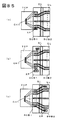
以下、本発明の実施の形態について、実施例の図面を参照して詳細に説明する。図1は本発明の第1実施例の画素構成を模式的に説明する縦電界型の液晶表示装置の一画素近傍の平面図である。図中、参照符号PXは画素電極、DLはドレイン線(映像信号線またはデータ線)、GLはゲート線(走査線)、SMは画素電極とドレイン線の間を遮光する遮光膜(シールドメタル)、STは基準電極層(導電層とも言う)、SD1はソース電極、SD2はドレイン電極、ASは半導体層、THはスルーホールを示す。なお、上記のゲート線、ドレイン線、各電極は、断面で説明する場合は電極層とも称する。
【0154】
図2は図1のI−I線に沿った断面図、図3は図1のII−II線に沿った断面図である。参照符号SUB1は第1の基板、STは基準電極層、O−PASは有機絶縁層、PASはパッシベーション層、ALは配向膜、CTは共通電極、CFはカラーフィルタ、BMはブラックマトリクス、SUB2は第2の基板を示す。
【0155】
図1〜図3において、この液晶表示装置は、第1の基板SUB1と第2の基板SUB2の対向間隙に液晶(以下、液晶層とも言う)LCを挟持している。第1の基板SUB1の内面には、第1の方向に延在し互いに並設された複数のゲート線GLおよびゲート線と交差して第2の方向に延在し互いに並設された複数のドレイン線GLを有する。
【0156】
ゲート線GLとドレイン線DLの交差部にはスイッチング素子として薄膜トランジスタTFTが設けられている。この薄膜トランジスタTFTはゲート線GLをゲート電極とし、ドレイン線DLから延びるドレイン電極SD2と半導体層AS、ソース電極SD1で構成される。なお、以下の実施例では、薄膜トランジスタについての説明は省略する。
【0157】
薄膜トランジスタTFTのソース電極SD1はスルーホールTHを介して画素電極層PXに接続されている。この画素電極層PXは画素領域のほとんどの部分に形成されて、液晶表示装置の表示領域を構成している。第1の基板SUB1の画素領域を含んでゲート線GL、ドレイン線DL、薄膜トランジスタTFT、および画素電極PXを形成する多層部分を電極形成層と言う。この電極形成層と第1の基板側SUB1との間に当該電極形成層に対して有機絶縁層O−PASで絶縁した基準電極層STを有している。
【0158】
なお、後述の各実施例を含めてO−PASとして有機絶縁層の代わりに無機絶縁層を用いてもよい。有機絶縁層とすることで、基準電極層とゲート線GLおよびドレイン線DLとの寄生容量をさらに低減することができる。
【0159】
上記電極形成層は、有機絶縁層O−PASの上層にゲート線層GL、ゲート絶縁層GI、ドレイン線層DL、薄膜トランジスタTFT、パッシベーション層PAS、および画素電極層PXをこの順で有する。そして、画素電極層PXと基準電極層STの間に画素の保持容量(所謂、Cstg)を形成する。すなわち、この保持容量はパッシベーション層PAS、ゲート絶縁層GI、および有機絶縁層O−PASを誘電体として画素電極層PXと基準電極層STの間に形成される。基準電極層STは画素領域のほとんどをカバーした広い面積に形成されている。
【0160】
この有機絶縁層O−PASの材料としては、例えばポリシラザンを用いる。これをSOG(スピンオングラス)法で塗布する。配線間の寄生容量低減には、低誘電率の有機膜材料が有効であり、例えばポリイミド、ポリアミド、ポリイミドアミド、アクリル、ポリアクリル、ベンゾシクロブテン、等、種々の有機材料を用いることができる。また、透過型液晶表示装置では透光性を有せしめることが必要で、透光率は高いことが望ましい。透光率の向上に有効なのは、既存の材料層を利用することである。すなわち、カラーフィルタ層を上記の有機絶縁層として利用すれば、透光性を阻害することが少ない。この有機絶縁層の形成プロセスを低減するためには当該層材料が感光性を有することが望ましい。この点は後述の各実施例でも同様である。
【0161】
ゲート絶縁層下でスルーホールを形成する構成では、フォトリソグラフィープロセス数が低減できるからである。また、ゲート絶縁層に設けたスルーホールと同位置で有機絶縁層にスルーホールを設ける場合には、当該ゲート絶縁層あるいはその上層の絶縁層からのスルーホール加工時に、上層の絶縁層をマスクとしたパターニング、あるいは一括加工等を採用できるため、この場合は感光性である必要はない。しかし、通常、同一のプロセス、材料にて種々の構成の製品を製造するため、多品種を同一製造ラインで製造するためには、感光性を有する材料を用いるのは望ましい。この点も後述の各実施例についても同様である。
【0162】
また、有機絶縁層O−PASの膜厚は、当業者であれば後述する実施例の開示内容に基づいて、各構成毎にシミュレーションにより容易に設定可能である。すなわち、この膜厚は、基板の平面構造、断面構造、有機絶縁層の誘電率などの値からの特性曲線から算出でき、これを利用して、配線抵抗、周辺の駆動回路の性能、使用する液晶材料、目標とする画質等に関する製品毎、あるいは設計思想に対応した範囲を選択することで実際の膜厚を設定することができる。これに関しては後述の各実施例においても同様である。
【0163】
このような構成としたことにより、保持容量に対する給電抵抗が大幅に低減され、画素の開口率と保持容量を両立した液晶表示装置を得ることができる。画素領域に給電線を設ける必要がないため、その場合には画素の開口率が向上する。また、画素電極と基準電極層の間に形成されるパッシベーション層、ゲート絶縁層、誘電率の小さい有機絶縁層で蓄積容量が形成される。液晶層からみた基準電極層までの距離を無機の絶縁層のみの場合に比べて大幅に離間させることが可能となり、液晶の駆動用電界への基準電極層の電界の影響が軽減される。
【0164】
また、本実施例では、基準電極層STはゲート線GLの延在方向と平行、かつ画素電極の形成領域に重畳してゲート線GLの延在方向に有するように構成しても良い。これにより、ゲート線GLと基準電極層の間の容量が低減され、寄生容量の増大を抑制することができ、また電位の安定化を図ることができる。
【0165】
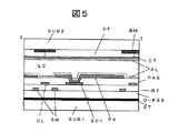
図4は本発明の第2実施例の画素構成を模式的に説明する縦電界型の液晶表示装置の一画素近傍の平面図、図5は図4のI−I線に沿った断面図、図6は図4のII−II線に沿った断面図である。図中の前記実施例の図面と同一参照符号は同一機能部分に相当する。
【0166】
本実施例では、基準電極層STが第1の基板SUB1のゲート線層GLとドレイン線DLおよび画素電極層PXの形成領域を含む領域に有する。保持容量は画素電極層PXと基準電極層STの間に形成される。なお、本実施例では、基準電極層STがゲート線層GLの下層に形成するため、両電極層の寄生容量を考慮して有機絶縁層O−PASの厚みは、例えば1μm以上とすることが望ましい。
【0167】
この構成により、第1実施例と同様の効果に加え、基準電極層STが、所謂べた電極であることで給電抵抗がさらに低減され、かつ給電方向の制限が無くなる。
【0168】
図7は本発明の第3実施例の画素構成を模式的に説明する縦電界型の液晶表示装置の一画素近傍の平面図、図8は図7のI−I線に沿った断面図である。図中の前記実施例の図面と同一参照符号は同一機能部分に相当する。画素形成層は、有機絶縁層0−PASの上層にゲート線層GL、ゲート絶縁層GI、ドレイン線層DL、薄膜トランジスタTFT、パッシベーション層PAS、画素電極PXをこの順で有する。画素領域における画素電極PXの全部または一部がパッシベーション層PASを貫通してゲート絶縁層GIに接している。
【0169】
本実施例の構成により、前記各実施例の効果に加え、基準電極層STと画素電極PXとの間に形成される蓄積容量を画素電極PXがパッシベーション層PASを貫通する面積で調整できる。
【0170】
図9は本発明の第4実施例の画素構成を模式的に説明する縦電界型の液晶表示装置の一画素近傍の図8のI−I線に沿った断面図である。図中の前記実施例の図面と同一参照符号は同一機能部分に相当する。
【0171】
画素形成層は、有機絶縁層O−PASの上層にゲート線層GL、ゲート絶縁層GI、ドレイン線層DL、薄膜トランジスタTFT、パッシベーション層PAS、画素電極PXをこの順で有し、画素領域における画素電極PXの全部または一部がパッシベーション層PASとゲート絶縁層GLとを貫通して有機絶縁層に接している。
【0172】
本実施例の構成により、基準電極層STと画素電極PXとの間に形成される蓄積容量を画素電極PXがパッシベーション層PASとゲート絶縁層GIとを貫通する面積で調整できる。
【0173】
図10は本発明の第5実施例の画素構成を模式的に説明する縦電界型の液晶表示装置の一画素近傍の平面図である。本実施例は上記第4実施例の変形例であり、画素電極PXの領域内の一部でゲート絶縁層GIを除去したものである。本実施例の効果は第4実施例と同様であり、加えてゲート絶縁層GIの欠如により透過率が向上する。
【0174】
図11は本発明の第6実施例の画素構成を模式的に説明する縦電界型の液晶表示装置の一画素近傍の平面図である。本実施例では、薄膜トランジスタTFTはゲート絶縁層GIの上にパッシベーション層PASに形成したスルーホールTHを介して画素電極PXと接続するソース電極SD1を有し、このソース電極SD1の一部を画素電極PXの領域内に拡大した。ソース電極SD1の拡大は、ゲート線GLまたはドレイン線DLに沿った延長部SD1Eとして形成するのが好適である。
【0175】
本実施例の構成により、前記各実施例の効果に加えてソース電極SD1の延長部SD1Eの長さ、または幅を変え、すなわちソース電極SD1が画素電極PXと重畳する面積を変えることで蓄積容量を調整できる。
【0176】
図12は本発明の第7実施例の画素構成を模式的に説明する縦電界型の液晶表示装置の一画素近傍の平面図、図13は図12のI−I線に沿った断面図、図14は図12のII−II線に沿った断面図である。図中の前記実施例の図面と同一参照符号は同一機能部分に相当する。
【0177】
本実施例の液晶表示装置は、第1の基板SUB1の画素領域を含んでゲート線層GL、ドレイン線層DL、薄膜トランジスタTFT、画素電極PXを形成する電極形成層と第1の基板SUB1側との間に当該電極形成層に対して第1の有機絶縁層O−PAS1で絶縁した基準電極層STを有する。画素形成層は、第1の有機絶縁層O−PAS1の上層にゲート線層GL、ゲート絶縁層GI、ドレイン線層DL、薄膜トランジスタTFT、パッシベーション層PAS、第2の有機絶縁層O−PAS2、画素電極PXをこの順で有する。そして、画素電極PXと基準電極層STで画素の保持容量を形成する。
【0178】
本実施例の構成により、画素の開口率が向上し、導電層の面積が大きいために給電抵抗が低減できる。また、スイッチング素子の上層にも有機絶縁層を設けた場合には、画素電極とドレイン線の重畳が可能となり、さらに開口率が向上する。画素電極とドレイン線を重畳した場合に、ドレイン線の延在方向近傍と画素電極の間の遮光層を省略できるため、またさらに開口率が向上する。
【0179】
また、前記基準電極層STがゲート線層GLと平行、かつ画素電極層PXの形成領域に重畳してゲート線層GLの延在方向に形成されている。これにより、ゲート線層と導電層の間の寄生容量が低減され、また電位の安定化を図ることができる。
【0180】
さらに、前記基準電極層が前記第1の基板SUB1のゲート線層GLとドレイン線層DLおよび画素電極層PXの形成領域を含む領域に有する。この構成により、基準電極層STが、所謂べた電極であることで給電抵抗がさらに低減され、かつ給電方向の制限が無くなる。
【0181】
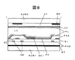
図15は本発明の第8実施例の画素構成を模式的に説明する縦電界型の液晶表示装置の一画素近傍の平面図、図16は図15のI−I線に沿った断面図、図17は図15のII−II線に沿った断面図である。図中の前記実施例の図面と同一参照符号は同一機能部分に相当する。
【0182】
本実施例は、前記第1の有機絶縁層をカラーフィルタCFとすることで、画素電極層PXと基準電極層STの間に形成される誘電率の小さい有機絶縁層O−PAS、パッシベーション層PAS、ゲート絶縁層DI、カラーフィルタ層CFで保持容量が形成されるため、基準電極層とゲート線およびドレイン線との寄生容量の増大を抑制できる。また、第1の基板SUB1にカラーフィルタ層CFを形成するため、第2の基板SUB2との位置合わせ裕度が大きくなり、画素の開口率が向上し、導電層の面積が大きいために給電抵抗が低減できる。
【0183】
図18は本発明の第9実施例の画素構成を模式的に説明する縦電界型の液晶表示装置の図15のI−I線に沿った断面図、図19は同じく図18のII−II線に沿った断面図である。図中の前記実施例の図面と同一参照符号は同一機能部分に相当する。
【0184】
図17に示した実施例では、カラーフィルタCFの境界を遮光するブラックマトリクスBMを第2の基板SUB2側に形成した。本実施例では、このブラックマトリクスBMを第1の基板SUB1側に設けたものである。
【0185】
また、第8及び第9実施例において、前記基準電極層STはゲート線層GLと平行、かつ画素電極層PXの形成領域に重畳してゲート線層GLの延在方向に形成されている。
【0186】
この構成により、ゲート線層GLと基準電極層STの間の寄生容量が低減される。また電位の安定化を図ることができる。
【0187】
また、基準電極層STを第1の基板SUB1のゲート線層GLとドレイン線層DLおよび画素電極層PXの形成領域を含む領域に有する、所謂べた電極として給電抵抗をさらに低減し、かつ給電方向の制限を無くすことができる。
【0188】
さらに、カラーフィルタ層CFとゲート絶縁層GIの間に、カラーフィルタ層CFを平坦化するオーバーコート層を形成してもよい。このとき、カラーフィルタ層CFとゲート絶縁層GIの間に基準電極層STを形成してもよい。
【0189】
図20は本発明の第10実施例の画素構成を模式的に説明する縦電界型の液晶表示装置の一画素近傍の平面図、図21は図20のIII −III に沿った断面図である。図中の前記実施例の図面と同一参照符号は同一機能部分に相当する。
【0190】
本実施例は、第1の基板SUB1の画素領域を含んでゲート線層GL、ドレイン線層DL、薄膜トランジスタTFT、画素電極層PXを形成する電極形成層と第1の基板側SUB1との間に当該電極形成層に対して第1の有機絶縁層O−PAS1で絶縁した第1の基準電極層STを形成してある。そして、第1の有機絶縁層O−PASA1の上層にゲート線層GL、ゲート絶縁層GI、ドレイン線層DL、薄膜トランジスタTFT、パッシベーション層PAS、第2の有機絶縁層O−PAS2、画素電極層PXをこの順で形成し、第2の有機絶縁層O−PAS2とパッシベーション層PASの間に画素電極PXと接続した容量電極層TEDを有してある。
【0191】
図22は本発明の第11実施例の画素構成を模式的に説明する図20のIII −III に沿った断面図である。図中の前記実施例の図面と同一参照符号は同一機能部分に相当する。本実施例は、図21に示した容量電極層TEDをゲート絶縁層GI上で第2の有機絶縁層O−PAS2の下層に形成した。
【0192】
図23は本発明の第12実施例の画素構成を模式的に説明する図20のIII −III に沿った断面図である。図中の前記実施例の図面と同一参照符号は同一機能部分に相当する。本実施例は、図21あるいは図22に示した容量電極層TEDを第1の有機絶縁層O−PASの上層でゲート絶縁層GIの下層に形成した。
【0193】
上記第10、第11、第12の実施例の構成により、画素の開口率が向上し、導電層の面積が大きいために給電抵抗が低減できる。また容量電極層TEDの面積、形状で蓄積容量を調整できる。さらに、薄膜トランジスタの上層にも有機絶縁層を設けた場合には、画素電極とドレイン線の重畳が可能となり、さらに開口率が向上する。画素電極とドレイン線を重畳した場合に、ドレイン線の延在方向近傍と画素電極の間の遮光層を省略できるため、またさらに開口率が向上する。
【0194】
なお、第1の基準電極層STはゲート線層GLと平行、かつ画素電極層PXの形成領域に重畳してゲート線層GLの延在方向に形成することができる。これにより、ゲート線層GLと第1の基準電極層STの間の寄生容量が低減され、蓄積容量の増大を抑制することができ、また電位の安定化を図ることができる。
【0195】
また、第1の基準電極層STを第1の基板SUB1のゲート線層GLとドレイン線層DLおよび画素電極層PXの形成領域を含む領域に形成してもよい。この構成により、第1の基準電極層STが、所謂べた電極であることで給電抵抗がさらに低減され、かつ給電方向の制限が無くなる。
【0196】
図24は本発明の第13実施例の画素構成を模式的に説明する縦電界型の液晶表示装置の一画素近傍の平面図、図25は図24のIII −III に沿った断面図である。図中の前記実施例の図面と同一参照符号は同一機能部分に相当する。本実施例では、例えば図20〜図23で説明した容量電極層TEDを画素領域におけるパッシベーション層PASと第2の有機絶縁層O−PASの間に形成し、スルーホールTH2を介して画素電極層PXに接続した。
【0197】
すなわち、薄膜トランジスタTFTは、ゲート絶縁層GIの上にパッシベーション層PASに形成したスルーホールTH1を介して画素電極PXと接続するソース電極を有し、容量電極層TEDはソース電極SD1に接続して画素電極PXの形成領域に有する。
【0198】
この構成により、前記容量電極層の大きさを変えることで保持容量を調整できる。なお、第1の有機絶縁層O−PASをカラーフィルタとすることもできる。
【0199】
この構成により、画素の開口率が向上し、導電層の面積が大きいために給電抵抗が低減できると共に、画素電極と基準電極層の間に形成される誘電率の小さい有機絶縁層、パッシベーション層、ゲート絶縁層、カラーフィルタ層で保持容量を形成した場合は、寄生容量の増大を抑制できる。また、第1の基板にカラーフィルタ層を形成するため、第2の基板との位置合わせ裕度が大きくなる。
【0200】
図26は本発明の第14実施例の画素構成を模式的に説明する縦電界型の液晶表示装置の一画素近傍の図24のIII −III に沿った断面図である。図中の前記実施例の図面と同一参照符号は同一機能部分に相当する。本実施例では、容量電極層TEDをゲート絶縁層GI上に有する。画素電極を第2の有機絶縁層O−PAS2とパッシベーション層PASに形成したスルーホールを介して容量電極層TEDに接続した。
【0201】
図27は本発明の第15実施例の画素構成を模式的に説明する縦電界型の液晶表示装置の一画素近傍の図24のIII −III に沿った断面図である。図中の前記実施例の図面と同一参照符号は同一機能部分に相当する。本実施例では、容量電極層TEDを第1の有機絶縁層O−PAS上に有し、画素電極PXを第2の有機絶縁層O−PAS2とパッシベーション層PASおよびゲート絶縁層GIを貫通して形成したスルーホールTH2を介して容量電極層TEDに接続した。
【0202】
上記第13〜第15の実施例の構成により、導電層と画素電極との間に形成される保持容量を容量電極TEDの面積で調整できる。
【0203】
また、第13〜第15の実施例における第1の有機絶縁層O−PAS1をカラーフィルタとしてもよい。
【0204】
この構成により、画素の開口率が向上し、導電層の面積が大きいために給電抵抗が低減できる。また、第1の基板にカラーフィルタ層を形成した場合は、第2の基板SUB2との位置合わせ裕度が大きくなる。
【0205】
図28は本発明の第16実施例の画素構成を模式的に説明する縦電界型の液晶表示装置の一画素近傍の平面図、図29は図28のIII −III に沿った断面図である。図中の前記実施例の図面と同一参照符号は同一機能部分に相当する。本実施例では、第1の基板の前記画素領域を含んで前記ゲート線、ドレイン線、スイッチング素子、画素電極を形成する電極形成層と前記第1の基板側との間に当該電極形成層に対して有機絶縁層で絶縁した第1の基準電極層を有する。
【0206】
上記電極形成層は、前記有機絶縁層O−PASの上層にゲート線層GL、ゲート絶縁層GI、ドレイン線層DL、薄膜トランジスタTFT、パッシベーション層PAS、画素電極層PXをこの順で有し、かつ有機絶縁層O−PASとパッシベーション層PASの間に画素電極層PXと接続した容量電極層TEDを形成してある。そして、画素電極層PXと第1の基準電極層STおよび容量電極層TEDで画素の保持容量を形成している。
【0207】
図29に示したように、容量電極層TEDをゲート絶縁層GI上に有し、ソース電極SD1を容量電極層TEDに接続した。スイッチング素子TFTは、ゲート絶縁層GIの上にパッシベーション層PASに形成したスルーホールTHを介して画素電極PXと接続するソース電極SD1を有し、容量電極層TEDはソース電極SD1に接続して画素領域に形成されている。
【0208】
この構成により、前記容量電極層の大きさを変えることで蓄積容量を調整できる。また、有機絶縁層O−PASをカラーフィルタ層とすることもできる。
【0209】
本実施例の構成により、画素の開口率が向上し、導電層の面積が大きいために給電抵抗が低減できる。容量電極層TEDの大きさを変えることで保持容量を調整できる。また、第1の基板にカラーフィルタ層を形成した場合は、第2の基板SUB2との位置合わせ裕度が大きくなる。
【0210】
図30は本発明の第17実施例の画素構成を模式的に説明する縦電界型の液晶表示装置の一画素近傍の図28のIII −III に沿った断面図である。図中の前記実施例の図面と同一参照符号は同一機能部分に相当する。本実施例では、容量電極層TEDを有機絶縁層O−PAS上に有し、ソース電極SD1をゲート絶縁層GIを貫通したスルーホールTHを介して容量電極層TEDに接続した。
【0211】
この構成により、容量電極層TEDと画素電極PXとの間に形成される保持容量を画素電極PXがパッシベーション層PASとゲート絶縁層GIとを貫通する面積で調整できる。また、有機絶縁層をカラーフィルタ層とすることもできる。
【0212】
本実施例の構成により、開口率が向上し、第1の基準電極層の面積が大きいために給電抵抗を低減できる。また、有機絶縁層をカラーフィルタ層とした場合は、第2の基板との位置合わせ裕度が大きくなる。
【0213】
図31は本発明の第18実施例の画素構成を模式的に説明する縦電界型の液晶表示装置の一画素近傍の平面図、図32は図31のIII −III に沿った断面図である。図中の前記実施例の図面と同一参照符号は同一機能部分に相当する。本実施例では、容量電極層TEDをゲート絶縁層GI上に有し、画素電極層PXをパッシベーション層PASを貫通したスルーホールTH2を介して容量電極層TEDに接続した。また、有機絶縁層O−PASをカラーフィルタ層とすることもできる。
【0214】
本実施例の構成により、第1の基準電極層STと画素電極層PXとの間に形成される保持容量を容量電極層TEDの面積で調整できる。また、有機絶縁層O−PASをカラーフィルタ層とすることもできる。
【0215】
図33は本発明の第19実施例の画素構成を模式的に説明する縦電界型の液晶表示装置の一画素近傍の図31のIII −III に沿った断面図である。図中の前記実施例の図面と同一参照符号は同一機能部分に相当する。本実施例では、容量電極層TEDを有機絶縁層O−PAS上に有し、画素電極層PXをパッシベーション層PASとゲート絶縁層GIを貫通したスルーホールTH2を介して容量電極層TEDに接続した。
【0216】
本実施例の構成により、第1の基準電極層STと画素電極層PXとの間に形成される保持容量を容量電極層TEDの面積で調整できる。また、有機絶縁層O−PASをカラーフィルタ層とすることもできる。
【0217】
図34は本発明の第20実施例の画素構成を模式的に説明する縦電界型の液晶表示装置の一画素近傍の平面図、図35は図34のIII −III に沿った断面図である。図中の前記実施例の図面と同一参照符号は同一機能部分に相当する。本実施例では、容量電極層TEDを第1の有機絶縁層O−PAS上に形成し、(34)、(23)において、前記容量電極層を第1の有機絶縁層上に有し、第1の基準電極層O−PAS2を貫通したスルーホールTH2を介して第1の基準電極層STに接続した。
【0218】
この構成により、蓄積容量を第1の基準電極層に接続した容量電極層の面積で調整できる。また、第1の基板にカラーフィルタ層を形成した場合は第2の基板SUB2との位置合わせ裕度が大きくなる。
【0219】
図36は本発明の第21実施例の画素構成を模式的に説明する縦電界型の液晶表示装置の一画素近傍の図34のIII −III に沿った断面図である。図中の前記実施例の図面と同一参照符号は同一機能部分に相当する。本実施例では、容量電極層TEDをゲート絶縁層GI上に有し、ゲート絶縁層GIを貫通したスルーホールTH2を介して第1の基準電極層STに接続した。
【0220】
本実施例の構成により、蓄積容量を第1の基準電極層に接続した容量電極層の面積で調整できる。また第1の基板にカラーフィルタ層を形成した場合は第2の基板SUB2との位置合わせ裕度が大きくなる。
【0221】
図37は本発明の第22実施例の画素構成を模式的に説明する縦電界型の液晶表示装置の一画素近傍の図34のIII −III に沿った断面図である。図中の前記実施例の図面と同一参照符号は同一機能部分に相当する。本実施例では、容量電極層TEDをパッシベーション層PAS上に有し、このパッシベーション層PASとゲート絶縁層GIおよび第1の有機絶縁層STを貫通したスルーホールTHを介して容量電極層TEDに接続した。
【0222】
この構成により、導電層と画素電極との間に形成される蓄積容量を第1の基準電極層に接続した容量電極層の面積で調整できる。また、第1の基板にカラーフィルタ層を形成した場合は第2の基板SUB2との位置合わせ裕度が大きくなる。
【0223】
本実施例の構成により、開口率が向上し、導電層の面積が大きいために給電抵抗が低減できる。また、第1の有機絶縁層O−PASをカラーフィルタとした場合は、第2の基板SUB2との位置合わせ裕度が大きくなる。
【0224】
図38は本発明の第23実施例の画素構成を模式的に説明する縦電界型の液晶表示装置の一画素近傍の平面図、図39は図38のIII −III に沿った断面図である。図中の前記実施例の図面と同一参照符号は同一機能部分に相当する。本実施例では、容量電極層TEDをゲート絶縁層GI上に有し、ゲート絶縁層GIと有機絶縁層O−PASを貫通するスルーホールTH2を介して第1の基準電極層STに接続した。
【0225】
本実施例の構成により、第1の基準電極層STと画素電極層PXとの間に形成される保持容量を第1の基準電極層STに接続した容量電極層TEDの面積で調整できる。また、第1の基板にカラーフィルタ層を形成した場合は第2の基板SUB2との位置合わせ裕度が大きくなる。
【0226】
図40は本発明の第24実施例の画素構成を模式的に説明する縦電界型の液晶表示装置の一画素近傍の図38のIII −III に沿った断面図である。図中の前記実施例の図面と同一参照符号は同一機能部分に相当する。本実施例では、容量電極層TEDを有機絶縁層O−PAS上に有し、有機絶縁層O−PASを貫通するスルーホールTH2を介して第1の基準電極層STに接続した。
【0227】
本実施例の構成により、第1の基準電極層STと画素電極層PXとの間に形成される保持容量を第1の基準電極層STに接続した容量電極層TEDの面積で調整できる。また、第1の基板にカラーフィルタ層を形成した場合は第2の基板SUB2との位置合わせ裕度が大きくなる。
【0228】
図41は本発明の第25実施例の画素構成を模式的に説明する縦電界型の液晶表示装置の一画素近傍の図38のIII −III に沿った断面図である。図中の前記実施例の図面と同一参照符号は同一機能部分に相当する。本実施例では、容量電極層TEDをゲート絶縁層GI上に有すると共に、有機絶縁層O−PAS上に第2の容量電極層TEDDを有する。画素電極PXをパッシベーション層PASに形成したスルーホールTH2を介して容量電極層TEDに接続すると共に、第2の容量電極層TEDDを有機絶縁層O−PASに形成したスルーホールTH3を介して第1の基準電極層STに接続した。
【0229】
この構成により、保持容量は容量電極層TEDと第2の容量電極層TEDDとの面積で調整できる。また、第1の基板にカラーフィルタ層を形成した場合は第2の基板SUB2との位置合わせ裕度が大きくなる。
【0230】
図42は本発明の第26実施例の画素構成を模式的に説明する縦電界型の液晶表示装置の一画素近傍の平面図、図43は図38のIII −III に沿った断面図である。図中の前記実施例の図面と同一参照符号は同一機能部分に相当する。本実施例は第1の基板SUB1に前記した各実施例中の容量電極層TEDを有する場合で、かつ有機絶縁層をカラーフィルタ層CFとした場合である。
【0231】
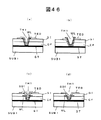
第1の基板SUB1上にカラーフィルタ層を設けた場合、スルーホールTH2の部分はカラーフィルタCFが存在しないため、この部分から光漏れが生じる。この光漏れを防止するため、容量電極TEDを第1の基準電極層STに接続するスルーホールTH2に金属遮光膜MLを設け、この金属遮光膜MLを介して容量電極層TEDを接続する。
【0232】
図44は本発明の第27実施例の画素構成を模式的に説明する縦電界型の液晶表示装置の一画素近傍の図42のIII −III に沿った断面図である。本実施例では、上記第26実施例における金属遮光膜MLを容量電極層TEDの上層に設けた。
【0233】
図45は本発明の第26実施例または第27実施例におけるスルーホールと金属遮光膜の平面図である。金属遮光膜MLの各辺はスルーホールTH2の開口部より大きく、少なくとも1μm以上の大きさに形成する。なお、カラーフィルタ層CF上にオーバーコート層を設けた場合も同様である。
【0234】
図46は本発明の第28実施例を説明する要部断面図であり、スルーホールと金属遮光膜の断面構造を示す図である。本実施例は、有機絶縁層をカラーフィルタとして、容量電極層TEDをソース電極SD1と同層のゲート絶縁層上に形成し、ソース電極SD1を遮光金属膜で形成したものである。スルーホール部での光漏れをスルーホール部に形成した遮光金属膜を用いて対策するものであり、この構成の一例を図42のTH2部を例に説明する。むろん、スルーホール部の遮光に用いる場合は他のスルーホールに用いてもよい。
【0235】
図46の(a)はスルーホールTH2に遮光金属膜MLをソース電極SD1により貫通させて第1の基準電極層STに接続し、このソース電極SD1の上に容量電極TEDを形成した。図46の(b)はスルーホールTH2に容量電極層TEDを形成した後、当該スルーホールTH2に遮光金属膜MLをソース電極SD1により形成した。図46の(c)はスルーホールTH2に遮光金属膜MLを形成した後、SD層を介して基準電極層TEDと接続した。
【0236】
また、図46の(d)は遮光金属膜MLをスルーホールTHに構成し、基準電極STと接続した後、遮光金属膜MLと基準電極層TEDを接続した。
【0237】
上記の各実施例において、基準電極層(あるいは第1の基準電極層)STをゲート線GLと平行、かつ画素電極PXの形成領域に重畳してゲート線GLの延在方向に形成することで、ゲート線層GLと基準電極層(あるいは第1の基準電極層)の間の寄生容量の増大を抑制することができ、また電位の安定化を図ることができる。
【0238】
また、上記の各実施例において、基準電極層(または第1の基準電極層)STを第1の基板SUB1のゲート線GLとドレイン線DLおよび画素電極PXの形成領域を含む領域に形成することで、当該基準電極層が、所謂べた電極であることで給電抵抗がさらに低減され、かつ給電方向の制限が無くなる。
【0239】
さらに、上記の各実施例において、ドレイン線DLの延在方向近傍と画素電極PXの間を遮光する遮光層DLを設けたものでは、ドレイン線DLと画素電極PXの間の光漏れを防止できる。
【0240】
図47は本発明の第29実施例の画素構成を模式的に説明するIPS型の液晶表示装置の一画素近傍の平面図、図48は図47のIII −III に沿った断面図である。図中の前記実施例の図面と同一参照符号は同一機能部分に相当する。本実施例は第1の基板SUB1と第2の基板SUB2の対向間隙に液晶を挟持し、第1の基板SUB1の内面に、第1の方向に延在し互いに並設された複数のゲート線GLおよびこのゲート線GLと交差する第2の方向に延在し互いに並設された複数のドレイン線DLと、ゲート線GLとドレイン線DLの交差部に設けられた複数の薄膜トランジスタTFTと、この薄膜トランジスタTFTで駆動される櫛型の画素電極PXと、画素電極PXとの間で画素駆動用の電界を生成する櫛型の対向電極CTとを少なくとも有している。
【0241】
画素電極PXと対向電極CTは同層に作ることもできる。
【0242】
そして、第1の基板SUB1の画素領域を含んでゲート線GL、ドレイン線DL、薄膜トランジスタTFT、画素電極PXを形成する電極形成層と第1の基板SUB1側との間に当該電極形成層に対して有機絶縁層O−PASで絶縁した基準電極層STを有し、画素電極PXと基準電極層STの間に画素の保持容量を形成している。
【0243】
そして、対向電極CTを有機絶縁層O−PAS上に有し、対向電極DTが有機絶縁層O−PASに形成したスルーホールTHを介して基準電極層STに接続されている。
【0244】
本実施例の構成により、十分な保持容量を形成できるため、画質の安定、向上が実現する。また保持容量を形成するための画素電極PXの面積を大きくする必要がないため開口率が向上する。また、基準電極層STの面積が大きいために給電抵抗を低減できる。
【0245】
図49は本発明の第30実施例の画素構成を模式的に説明するIPS型の液晶表示装置の一画素近傍の図47のIV−IVに沿った断面図である。対向電極CTはゲート絶縁層GI上に有し、対向電極CTがゲート絶縁層GIと有機絶縁層O−PASに形成したスルーホールTHを介して基準電極層STに接続されている。
【0246】
本実施例の構成により、保持容量が画素電極PXと誘電率の小さい有機絶縁層O−PASを介した基準電極層STとの間に形成。保持容量を形成するための画素電極PXの面積を大きくする必要がないため開口率が向上する。また、基準電極層STの面積が大きいために給電抵抗を低減できる。
【0247】
図50は本発明の第31実施例の画素構成を模式的に説明するIPS型の液晶表示装置の一画素近傍の図47のIV−IVに沿った断面図である。本実施例では、対向電極CTをパッシベーション層PAS上に有し、この対向電極をパッシベーション層PASとゲート絶縁層GIおよび有機絶縁層O−PASに形成したスルーホールTHを介して基準電極層STに接続されている。
【0248】
本実施例の構成により、保持容量が画素電極PXと誘電率の小さい有機絶縁層O−PASを介した基準電極層STとの間に形成される。保持容量を形成するための画素電極PXの面積を大きくする必要がないため開口率が向上する。また、基準電極層STの面積が大きいために給電抵抗を低減できる。
【0249】
また、上記第29〜第30実施例において、基準電極層STはゲート線GLと平行、かつ画素電極PXおよび対向電極CTの形成領域に重畳してゲート線GLの延在方向に形成してもよい。
【0250】
この構成により、ゲート線層GLと基準電極層STの間の寄生容量が低減され、保持容量の増大を抑制することができ、また電位の安定化を図ることができる。
【0251】
さらに、上記第29〜第30実施例において、基準電極層STを第1の基板SUB1のゲート線層GLとドレイン線層DL、画素電極PXおよび対向電極CTの形成領域を含む領域に形成することもできる。
【0252】
この構成により、基準電極層STが、所謂べた電極であることで給電抵抗がさらに低減され、かつ給電方向の制限が無くなる。また、有機絶縁層O−PASの層厚を厚くすることで、基準電極層の液晶駆動電界への影響を低減できる。有機絶縁層P−PASに代えてカラーフィルタとすることもでき、またカラーフィルタにオーバーコートを形成した場合はカラーフィルタ層の下層に基準電極層を設けることが望ましい。
【0253】
図51は本発明の第32実施例の画素構成を模式的に説明するIPS型の液晶表示装置の一画素近傍の平面図、図52は図51のV−V線に沿った断面図である。本実施例では、対向電極CTを有機絶縁層O−PAS上に有すると共に、ドレイン線DLと交差して隣接画素領域に延在し、当該隣接画素領域の基準電極層に有機絶縁層O−PASに形成したスルーホールTHを介して接続されている。
【0254】
本実施例の構成により、仮にスルーホールTHの形成が不十分であっても隣接画素側から基準電極層STを通して給電がなされる。
【0255】
図53は本発明の第33実施例の画素構成を模式的に説明するIPS型の液晶表示装置の一画素近傍の図51のV−V線に沿った断面図である。本実施例では、対向電極CTはゲート絶縁層GI上に有し、有機絶縁層O−PAS上に一方のドレイン線DLと交差して隣接画素領域に延在する容量電極層TEDを有する。対向電極層CTはゲート絶縁層GIと有機絶縁層O−PASに形成したスルーホールTHを介して第1の基準電極層STに接続している。
【0256】
この構成により、仮にスルーホールTHの形成が不十分であっても隣接画素側から第2に基準電極層TEDを通して給電がなされる。また、各対向電極と各基準電極とを接続するスルーホールを各画素毎に複数形成することで、当該電極層間の接続の信頼性を向上できる。
【0257】
図54は本発明の第34実施例の画素構成を模式的に説明するIPS型の液晶表示装置の一画素近傍の図51のV−V線に沿った断面図である。本実施例では対向電極CTはパッシベーション層PAS上に有し、有機絶縁層O−PAS上に一方のドレイン線DLと交差して隣接画素領域に延在する容量電極層TEDを有する。対向電極層CTはパッシベーション層PAS、ゲート絶縁層GI、有機絶縁層O−PASに形成したスルーホールTHを介して第1の基準電極層STに接続している。
【0258】
この構成により、仮にスルーホールの形成が不十分であっても隣接画素側から容量電極層TEDを通して給電がなされる。
【0259】
図55は本発明の第35実施例の画素構成を模式的に説明するIPS型の液晶表示装置の一画素近傍の図51のV−V線に沿った断面図である。本実施例では図54に示した第34実施例の第1の基準電極層STの下層で前記第1の基板SUB1の上にカラーフィルタ層を有する。
【0260】
この構成により、前記実施例の効果に加え、カラーフィルタ層CFが第1の基準電極STで液晶層と隔離されるため、カラーフィルタ層CFの構成材料による液晶の汚染が阻止される。
【0261】
図56は図47〜図55の実施例の変形例を説明するIPS型の液晶表示装置の一画素近傍の平面図である。すなわち、各画素の対向電極CTと基準電極STとを接続するスルーホールTHを各画素毎に複数形成することで、当該電極層間の接続の信頼性を向上できる。
【0262】
図57は本発明の第36実施例の画素構成を模式的に説明するIPS型の液晶表示装置の一画素近傍の平面図、図58は図57のVI−VI線に沿った断面図である。本実施例では、対向電極CTは有機絶縁層O−PAS上にゲート線GLの延在方向と平行で、隣接する画素領域にわたって形成され、各画素領域における基準電極STには有機絶縁層O−PASに形成したスルーホールTHを介して接続する。
【0263】
この構成により、保持容量は対向電極CTと画素電極PXの重畳部分で形成され、ゲート絶縁層GIは保持容量の誘電体となる。保持容量を増大させる場合に好適である。
【0264】
図59は本発明の第37実施例の画素構成を模式的に説明するIPS型の液晶表示装置の一画素近傍の図57のVI−VI線に沿った断面図である。本実施例では、対向電極CTは例えばゲート絶縁層上に有し、有機絶縁層O−PAS上にゲート線GLの延在方向と平行で、有機絶縁層O−PASの隣接する画素領域にわたって形成された容量電極層TEDを有している。対向電極CTは各画素領域において基準電極層に有機絶縁層O−PASとゲート絶縁層GIとを貫通して形成したスルーホールTHを介して接続され、容量電極層TEDと画素電極層PXの重畳部分で保持容量が形成される。
【0265】
この構成により、ゲート絶縁層GIが保持容量の誘電体となり、櫛歯状の画素電極となっている。
【0266】
図60は本発明の第38実施例の画素構成を模式的に説明する変形IPS型の液晶表示装置の一画素近傍の平面図、図61は図60のVII −VII 線に沿った断面図、図62は図60のVIII−VIII線に沿った断面図である。本実施例では、画素電極PXはゲート絶縁層GI上に、所謂ヘリングボーン形状に形成されている。ソース電極SD1はゲート絶縁層GI上に形成され、このソース電極SD1に画素電極が重畳している。対向電極CTは有機絶縁層O−PAS上に有し、スルーホールTH2で基準電極層STに接続し、対向電極CTと前記画素電極とで保持容量を形成する。
【0267】
本実施例の構成により、ゲート絶縁層GIが保持容量の誘電体となり、ヘリングボーン形状の画素電極としたことによる保持容量の低下を増大させることができる。
【0268】
図63は本発明の第39実施例の画素構成を模式的に説明する変形IPS型の液晶表示装置の一画素近傍の図63のVII −VII 線に沿った断面図である。本実施例では、ソース電極SD1をゲート絶縁層GI上に形成し、パッシベーション層PAS上に形成した画素電極PXとスルーホールTH1で接続している。他の構成は図61と同様である。
【0269】
本実施例により、ゲート絶縁層GIが保持容量の誘電体となっている。
【0270】
図64は本発明の第40実施例の画素構成の要部を模式的に説明する変形IPS型の液晶表示装置の薄膜トランジスタTFT部分の平面図である。本実施例では、ゲート絶縁層GI上に形成する薄膜トランジスタTFTのソース電極SD1の面積を変えることで保持容量を調整できるようにした。
【0271】
本発明の他の実施例においても、本概念で保持容量を調整することが出来る。
【0272】
図65は本発明の第41実施例の画素構成の要部を模式的に説明する変形IPS型の液晶表示装置の一画素近傍の平面図、図66は図65のIX−IX線に沿った断面図である。本実施例は、画素電極PXはゲート絶縁層GI上に、所謂ヘリングボーン形状に形成されている。ソース電極SD1はゲート絶縁層GI上に形成され、このソース電極SD1に画素電極が重畳している。有機絶縁層O−PASの下層には基準電極が形成され、この基準電極を対向電極と兼用する基準/対向電極層ST/CTとしている。この基準/対向電極層ST/CTと画素電極PXで保持容量を形成する。
【0273】
本実施例により、対向電極層CTの形成を不要とし、保持容量に対する給電抵抗が大幅に低減され、画素の開口率の低下のない液晶表示装置を得ることができる。
【0274】
また、基準/対向電極層ST/CTは例えばゲート線GLと平行、かつ画素電極PXの形成領域に重畳して前記ゲート線GLの延在方向に有する。
【0275】
この構成により、画素毎に独立した基準/対向電極層を要せず、ゲート線層GLと基準/対向電極層ST/CTとの間の容量が低減され、寄生容量の増大を抑制することができ、また電位の安定化を図ることができる。
【0276】
また、基準/対向電極層ST/CTは第1の基板SUB1のゲート線GLとドレイン線DLおよび画素電極PXの形成領域を含む全領域に有する。
【0277】
この構成により、基準/対向電極層ST/CTが、所謂べた電極であることで給電抵抗がさらに低減され、かつ給電方向の制限が無くなる。
【0278】
図67は本発明の第42実施例の画素構成の要部を模式的に説明する変形IPS型の液晶表示装置の一画素近傍の図65のIX−IX線に沿った断面図である。本実施例では、画素電極PXはゲート絶縁層GI上に、所謂ヘリングボーン形状に形成されている。ソース電極SD1はゲート絶縁層GI上に形成され、このソース電極SD1に画素電極が重畳している。本実施例は、図66の構成における画素電極PXの下層の有機絶縁層O−PASの全部または一部を除去したものに相当する。
【0279】
この構成により、画素電極PXと基準/対向電極層ST/CTとの間に生成される電界強度が増大し、駆動電圧を低減することができる。
【0280】
図68は本発明の第43実施例の画素構成の要部を模式的に説明する変形IPS型の液晶表示装置の一画素近傍の平面図、図69は図68のX−X線に沿った断面図である。本実施例は、有機絶縁層O−PASの上に対向電極層CTを有し、かつこの対向電極層CT上にゲート線GLの延在方向と平行に当該対向電極を隣接する画素電極に接続する接続線GLLを有する。
【0281】
図70は本発明の第44実施例の画素構成の要部を模式的に説明する変形IPS型の液晶表示装置の一画素近傍の図68のX−X線に沿った断面図である。本実施例は、対向電極層CTと有機絶縁層O−PASの間にゲート線GLの延在方向と平行に当該対向電極層CTを隣接する画素電極層PXに接続する接続線GLLを有する。
【0282】
上記第43実施例と第44実施例の構成により、仮にスルーホールの形成が不十分であっても隣接画素側から導電層を通して給電がなされる。また、各対向電極層CTと基準電極STとを接続するスルーホールTHを各画素毎に複数形成することで、当該電極層間の接続の信頼性を向上できる。
【0283】
図71は本発明の第45実施例の画素構成の要部を模式的に説明する変形IPS型の液晶表示装置の一画素近傍の平面図、図72は図71のXI−XI線に沿った断面図である。本実施例では、基準電極層と対向電極を兼用する基準/対向電極層ST/CTを有し、有機絶縁層O−PASは画素領域内の一部で除去されている。
【0284】
図73は本発明の第46実施例の画素構成の要部を模式的に説明する変形IPS型の液晶表示装置の一画素近傍の図68のXI−XI線に沿った断面図である。本実施例は、有機絶縁層O−PAS上に対向電極CTを有し、有機絶縁層O−PASの一部を画素領域内で除去した。
【0285】
上記第45実施例および第46実施例の構成により、画素領域内に駆動電圧の異なる複数の領域を形成でき、マルチドメイン効果を得ることができる。
【0286】
図74は本発明の第47実施例の画素構成の要部を模式的に説明する他の変形IPS型の液晶表示装置の一画素近傍の平面図、図75は図74のXII −XII 線に沿った断面図である。
【0287】
本実施例は、第1の基板SUB1と第2の基板SUB2の対向間隙に液晶を挟持し、前記第1の基板の内面に、第1の方向に延在し互いに並設された複数のゲート線および前記ゲート線と交差する第2の方向に延在し互いに並設された複数のドレイン線と、前記ゲート線とドレイン線の交差部に設けられた複数のスイッチング素子と、前記アクティブ素子で駆動される画素電極と前記画素電極との間で画素駆動用の電界を生成する対向電極とを少なくとも有し、前記複数の画素電極で画素領域が構成される液晶表示装置である。
【0288】
また電極形状は、画素電極PXを平面状、対向電極CTをヘリングボーン状として、図60、65、68あるいは71の逆となるよう構成しても良い。この場合、ゲート線GLおよびドレイン線DLからの漏洩電界を対向電極CTでシールドできるようになるため、画質の一層の向上が実現する。
【0289】
第1の基板SUB1の画素領域を含んでゲート線GL、ドレイン線DL、薄膜トランジスタTFT、画素電極PXを形成する電極形成層と第1の基板SUB1側との間に当該電極形成層に対して第1の絶縁層O−PAS1で絶縁した基準電極層STを有する。
【0290】
電極形成層は、有機絶縁層O−PAS1の上層にゲート線GL、ゲート絶縁層GI、パッシベーション層PAS、第2の有機絶縁層O−PAS2、対向電極CTをこの順で積層してある。対向電極層CTは、画素領域のゲート線GLの延在方向に隣接する画素領域およびドレイン線DLの延在方向に隣接する画素領域にわたって共有されている。そして、対向電極層CTは、第2の有機絶縁層O−PAS2、パッシベーション層PAS、ゲート絶縁層GI、第1の有機絶縁層O−PAS1を貫通するスルーホールTHを介して接続され、画素電極PXと基準電極層STの間に画素の保持容量を形成する。
【0291】
本実施例の構成により、ゲート線GLおよびドレイン線DLからの漏洩電界を対向電極CTでシールドできるようになるため、画質の一層の向上が実現する。
【0292】
図76は本発明の第48実施例の画素構成の要部を模式的に説明する他の変形IPS型の液晶表示装置の一画素近傍の図74のXII −XII 線に沿った断面図である。本実施例は、画素電極PXの下層、かつ第1の有機絶縁層O−PAS1とゲート絶縁層GIの間に基準電極層STとスルーホールTHを介して接続した容量電極層TEDを有する。
【0293】
この構成により、保持容量を容量電極層TEDの面積で増加させ、調整することができる。
【0294】
図77は本発明の第49実施例の画素構成の要部を模式的に説明する他の変形IPS型の液晶表示装置の一画素近傍の図74のXII −XII 線に沿った断面図である。本実施例は、画素電極PX下の保持容量を形成する部分の第1の有機絶縁層O−PAS1を除去した。
【0295】
この構成により、誘電率が小さい有機絶縁層の欠如で画素電極と基準電極層の間に形成される保持容量を増大させることができる。
【0296】
図78は本発明の第50実施例の画素構成の要部を模式的に説明する他の変形IPS型の液晶表示装置の一画素近傍の図74のXII −XII 線に沿った断面図である。本実施例は、画素電極PXの上層にある対向電極CTの下層にある第2の有機絶縁層O−PAS2の一部を除去した。
【0297】
この構成によっても、誘電率が小さい有機絶縁層の欠如で画素電極と基準電極層の間に形成される保持容量を増大させることができる。
【0298】
図79は本発明の第51実施例の画素構成の要部を模式的に説明する他の変形IPS型の液晶表示装置の一画素近傍の図74のXII −XII 線に沿った断面図である。本実施例は、画素電極PXの下層にあるゲート絶縁層GIと第1の有機絶縁層O−PAS1の間に容量電極TEDを設けた。この容量電極TEDは図示しない位置で対向電極CTに接続される。また、容量電極TEDをゲート線GLの延在方向に平行に形成して画素間で共有としてもよい。
【0299】
この構成により、保持容量を容量電極TEDの面積で増加させ、あるいは調整できる。
【0300】
次に、本発明の液晶表示装置の他の構成部分の実施例を説明する。
【0301】
図80は本発明の液晶表示装置の基板構成の説明図である。液晶表示装置PNLは第1の基板SUB1と、この第1の基板SUB1よりも小サイズの第2の基板SUB2を液晶を介して貼り合わせて構成される。第1のSUB1の一辺とこの辺に隣接する他の辺には端子領域(ドレイン線側端子領域TMD、ゲート線側端子領域TMG)が形成され、重ね合わせられた第2の基板SUB2の大部分に有効表示領域を有する。
【0302】
図81は端子領域における第1の基板上に駆動回路を搭載したテープキャリアパッケージを実装した状態の説明図である。ドレイン線側端子領域TMDとゲート線側端子領域TMGのそれぞれに複数のテープキャリアパッケージTCP(ドレイン駆動回路チップCH2を搭載したドレイン線駆動用テープキャリアパッケージ、ゲート駆動回路チップCH1を搭載したゲート線駆動用テープキャリアパッケージ)が搭載される。
【0303】
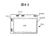
図82は端子領域における第1の基板上に駆動回路チップを直接実装した状態の説明図である。ドレイン線側端子領域TMDに複数のドレイン線駆動回路チップCH2を、ゲート線側端子領域TMGに複数のゲート線駆動回路チップCH1が搭載される。この実装方式をFCA方式(またはCPG方式)と称する。
【0304】
図83は二枚の基板の間に液晶を注入して封止する液晶封入口の配置例の説明図である。この例では、駆動回路チップを搭載しない辺に2つの液晶封入口INJを設けている。この液晶封入口INJの数や設置位置は液晶表示装置PNLのサイズにより設定され、1つでもよく、また3以上とすることもできる。
【0305】
図84は本発明の液晶表示装置の模式断面図である。第1の基板SUB1の内面には基準電極層STとその上層に有機絶縁層O−PASを有している。他の層や電極は図示を省略してある。第1の基板SUB1と第2の基板SUB2の間には液晶LCが封入され、有効表示領域の周囲をシール材SLで封止してある。
【0306】
図85はテープキャリアパッケージ方式で実装したゲート駆動回路の端子領域を模式的に説明する平面図である。図85(a)〜(c)ではテープキャリアパッケージTCPに搭載された駆動回路チップCH1の端子は第1の基板SUB1側に引き出されたゲート線の端子部に接続される。基準電極STへの接続は有機絶縁層O−PASを除去して接続される。この有機絶縁層O−PASの除去部分をXPで示す。図85(a)はこの除去部分XPをシール材SLの外側で、かつテープキャリアパッケージTCPの下側に配置した状態を示す。
【0307】
図85(b)は有機絶縁層O−PASの除去部分XPをシール材SLの外側で、かつテープキャリアパッケージTCPから外れた部分に配置した状態を示す。そして、図85(c)は有機絶縁層O−PASの除去部分XPをシール材SLの内側に配置した状態を示す。
【0308】
図86はFCA方式で駆動回路チップを実装した端子領域を模式的に説明する平面図である。図86(a)はシール材SLの外側で有機絶縁層O−PASを除去し、この除去部分XPで駆動回路チップの基準電極層への給電端子を接続した。図86(b)はシール材SLの中で有機絶縁層O−PASを除去し、この除去部分XPで駆動回路チップの基準電極層への給電端子を接続した。基準電極層への給電線の幅は、給電抵抗を低減するために他の信号線の幅より太いことが望ましい。
【0309】
図87は液晶表示装置の制御回路にある基準電位生成回路からフレキシブルプリント基板等で給電する方式とした場合の端子領域を模式的に説明する平面図である。フレキシブルプリント基板FPCに基準電極給電配線STLを設け、液晶表示装置の制御回路にある基準電位生成回路からフレキシブルプリント基板FPCを経由して第1の基板SUB1に引き出した基準電極の端子に給電する。図87(a)はテープキャリアパッケージ実装方式、同(b)はFCA方式にこの給電方式を適用した場合を示す。このように、基準電極層STへの給電を駆動回路チップCH1を経由せずにフレキシブルプリント基板FPCで行うことでさらに低抵抗の給電を行うことができる。GDLはゲート線への給電配線を示す。
【0310】
図88は基準電極への給電端子の形成の第1例を説明する液晶表示装置の模式平面図である。縦電界方式とIPS(変形IPS方式、他の変形IPS方式も含む)の何れにおいても、その基準電極STの周辺をパターニングして引出し端子STTを形成し、これに前記図84〜図87に示した構成で当該基準電極STに給電を行うようにした。
【0311】
図89は基準電極への給電端子の形成の第2例を説明する液晶表示装置の模式平面図、図90は図89のA部分を拡大した要部断面図である。特に、第2の基板SUB2側の共通電極を有する縦電界方式では、基準電極STのコーナー部にパターニングで接続部分STCを形成し、この接続部分STCで導電ペーストAGを介して共通電極STに基準電極STを接続する。基準電極STへの給電は共通電極で行われる。接続部分STCは全コーナーでなくてもよく、コーナー部の一箇所、2箇所、3箇所であってもよい。
【0312】
図91は基準電極への給電端子の形成の第3例を説明する液晶表示装置の模式断面図、図92は図91の給電端子部分を拡大した要部断面図である。基準電極STへの給電端子STTは基準電極STとは別途に形成してもよい。また、シールSL内でゲート線あるいはドレイン線等の他の配線と接続した配線で引き出してもよい。このとき、両者の接続抵抗に配慮する。給電端子STTが非Al系金属(Cr、Mo、Ti、Ta、W、Zr等の高融点金属、あるいはそれらの合金等の透明電極である基準電極STとの接触抵抗が低い場合に好適な構成である。なお、給電端子STTを透明導電膜(ITO、IZO等)で形成してもよい。
【0313】
図93は基準電極への給電端子の形成の第4例を説明する液晶表示装置の模式断面図である。給電端子STTと基準電極STの接触抵抗が高い場合、補助接続線STT’を介して接続するのが好ましい。例えば、給電端子STTがAlの場合、補助接続線STT’は非Alとする。また、補助接続線STT’にも透明導電膜を用いる場合、およびAl系の給電端子STTと基準電極STを直接接続する場合でも、通常の信号線と異なり、多点給電が可能であるため図93の構成が可能である。
【0314】
図94は第1の基板に形成する有機絶縁層をカラーフィルタとした場合の有効表示領域外周の構成例を説明する液晶表示装置の模式断面図である。有機絶縁層をカラーフィルタCFとした場合には、有効表示領域外周に3原色(R,G,B)のカラーフィルタ材料CF1、またはその少なくとも1つと他の少なくとも1つCF2を積層する。これにより、有効表示領域外周に遮光層を形成できる。また、有効表示領域外周に2つのカラーフィルタ材料を積層する場合、CF1をRとしCF2をGまたはBとする。Rのカラーフィルタ材料はR光以外を吸収するため、Rを吸収するGまたはBのカラーフィルタ材料を組み合わせることでR,G,Bの各色光を吸収できる。
【0315】
図95は第1の基板に形成する有機絶縁層をカラーフィルタとした場合の有効表示領域外周の他の構成例を説明する液晶表示装置の模式断面図である。シールSLとそのの外周部分に図94で説明したようなCF2を積層した場合で、カラーフィルタ層(CF1,CF2)と有効表示領域を含めや全カラーフィルタ層を保護するために、このカラーフィルタ層(CF、CF1,CF2)の上にオーバーコート層OCを形成するのが望ましい。
【0316】
図96はシールとその外周部分および有効表示領域の全てにカラーフィルタを形成した構成例を説明する液晶表示装置の模式断面図である。この場合も、シールとその外周部分および有効表示領域の全てのカラーフィルタ層CFの上にオーバーコート層OCを形成するのが望ましい。
【0317】
図97は第1の基板に形成した各種の引出し端子や給電端子に駆動回路を実装する場合の位置合わせ方式の説明図であり、同図(a)はテープキャリアパッケージを用いた場合、同(b)はFCA方式を採用した場合を示す。同図(a)および同(b)において、カラーフィルタCFをシール外にも設けた場合、駆動回路チップCH1を搭載したテープキャリアパッケージTCPまたはFCAの駆動回路チップCH1と第1の基板に形成した各種の引出し端子や給電端子とのアライメントを取るアライメントマークAM近傍では、カラーフィルタCFに除去部分XPを形成するのが望ましい。これにより、アライメントマークAMの光学認識の際の誤差の発生を防ぎ、実装精度を確保できる。
【0318】
図98は第1の基板に形成した基準電極層の電食を防止する構成とした液晶表示装置の模式断面図である。シールSLの外側にある基準電極層STの電食を防止するため、基準電極層STの端部まで有機絶縁層O−PASを被覆する。
【0319】
図99は第1の基板に形成する有機絶縁層をカラーフィルタとした場合のカラーフィルタの形成例を説明する模式平面図である。同図に示したように、カラーフィルタCFはシールSLの内側のみに形成することもできる。カラーフィルタCFは光の波長を選択する機能を果たすために多量の顔料あるいは染料を含む。このため、無色の有機絶縁層に比べて吸湿性が高くなる傾向を有する。
【0320】
高温高湿となり得るシールSLの外部の領域にカラーフィルタCFがあると、当該部分のカラーフィルタCFは吸湿で膨潤し、しわ状となり、その上層に形成する引出し線や給電線の断線を招く場合がある。これを防止するために、カラーフィルタCFをシールSLの内側にのみ形成する。
【0321】
図100は第1の基板に形成する有機絶縁層をカラーフィルタとした場合の構成例を説明する模式平面図である。図99で説明した構成において、基準電極層STをシールSLの外側まで形成したとき、走査信号線等との短絡を防止するためにカラーフィルタCFの非形成部にはオーバーコート層OCを形成する。これにより、上記の短絡を防止できる。
【0322】
図101は第1の基板に形成する有機絶縁層をカラーフィルタとした場合の他の構成例を説明する模式平面図である。第1の基板SUB1の有効表示領域内にのみカラーフィルタ層CFを形成した場合、基準電極層STも当該有効表示領域内にのみ形成する。なお、基準電極層STは他の配線と交差させないでカラーフィルタCFからはみ出して形成してもよい。
【0323】
図102は第1の基板に形成する有機絶縁層をカラーフィルタとした場合のさらに他の構成例を説明する模式平面図である。図101において、基準電極層STは他の配線と交差させないでカラーフィルタCFからはみ出して形成した場合には、図102のようにカラーフィルタCFおよび基準電極STを被覆してオーバーコート層OCを形成する。
【0324】
図103は本発明の液晶表示装置を透過型表示モジュールとして用いた一配置例を説明する模式断面図である。第1の基板SUB1と第2の基板SUB2の貼り合わせで形成した液晶表示装置の第1の基板SUB1の背面にバックライトBLを設置する。この配置例は透過型表示モジュールの典型的な構成である。バックライトBLからの照明光L1は液晶表示装置を透過するときに当該液晶表示装置で変調され、第2の基板側SUB2から出射する。
【0325】
図104は本発明の液晶表示装置を透過型表示モジュールとして用いた他の配置例を説明する模式断面図である。第1の基板SUB1と第2の基板SUB2の貼り合わせで形成した液晶表示装置の第2の基板SUB2の表面にフロントライトFLを設置する。フロントライトFLからの照明光L1は液晶表示装置を透過するときに当該液晶表示装置で変調され、第1の基板側SUB1から出射する。
【0326】
図105は本発明の液晶表示装置を反射型表示モジュールとして用いた第1の配置例を説明する模式断面図である。第1の基板SUB1と第2の基板SUB2の貼り合わせで形成した液晶表示装置の第1の基板SUB1に有する基準電極STを反射性金属層で構成する。第2の基板SUB2に入射した外光L2は基準電極STで反射し、第2の基板側から出射する光L2は液晶表示装置内を透過するときに当該液晶表示装置に形成された電子潜像で変調される。
【0327】
図106は本発明の液晶表示装置を反射型表示モジュールとして用いた第2の配置例を説明する模式断面図である。第1の基板SUB1と第2の基板SUB2の貼り合わせで形成した液晶表示装置の第2の基板SUB2の表面にフロントライトFLを設置する。フロントライトFLから出射した光L2は第1の基板の内面に有する反射性金属層で構成した基準電極STで反射し、第2の基板側からフロントライトFLを通って出射する。この光L2は液晶表示装置内を透過するときに当該液晶表示装置で変調される。
【0328】
図107は本発明の液晶表示装置を反射型表示モジュールとして用いた第3の配置例を説明する模式断面図である。第1の基板SUB1と第2の基板SUB2の貼り合わせで形成した液晶表示装置の第2の基板SUB2の表面に反射層RTを設けている。第1の基板SUB1から入射した外光L2は反射層RTで反射し、第1の基板側から出射する。この光L2は液晶表示装置内を透過するときに当該液晶表示装置で変調される。
【0329】
図108は本発明の液晶表示装置を反射型表示モジュールとして用いた第4の配置例を説明する模式断面図である。第1の基板SUB1と第2の基板SUB2の貼り合わせで形成した液晶表示装置の第2の基板SUB2の内面に設ける共通電極CTを反射性金属層で構成する。第1の基板SUB1から入射した外光L2は共通電極CTで反射し、第1の基板側から出射する。この光L2は液晶表示装置内を透過するときに当該液晶表示装置で変調される。
【0330】
図109は本発明の液晶表示装置を反射型表示モジュールとして用いた第5の配置例を説明する模式断面図である。第1の基板SUB1と第2の基板SUB2の貼り合わせで形成した液晶表示装置の第1の基板SUB1の背面にフロントライトFLを設置する。また、第2の基板SUB2の内面に設ける共通電極CTを反射性金属層で構成する。フロントライトFLから第1の基板SUB1に入射した外光L2は共通電極CTで反射し、第1の基板側からフロントライトFLを通して出射する。この光L2は液晶表示装置内を透過するときに当該液晶表示装置で変調される。
【0331】
図110は本発明の液晶表示装置を透過/反射型表示モジュールとして用いた一配置例を説明する模式断面図である。第1の基板SUB1と第2の基板SUB2の貼り合わせで形成した液晶表示装置の第1の基板SUB1に有する基準電極STは反射性金属層で構成し、その各画素対応で部分的な開口(スリット孔、あるいはドット孔などでもよい)を有している。
【0332】
反射型モードとして動作する場合は、第2の基板SUB2から入射した外光L2が基準電極STで反射し、第2の基板SUB2から出射する。透過型モードとして動作する場合は、第1の基板SUB1の背面に設置したバックライトBLからの光L1が基準電極STの開口を通って第2の基板SUB2を通して出射する。この光L2あるいはL1は液晶表示装置内を透過するときに当該液晶表示装置で変調される。また、基準電極STを開口を持つ反射性金属層に代えて半透過性反射層とすることもできる。なお、反射型と透過型の両モードで動作することはもちろんである。
【0333】
図111は本発明の液晶表示装置を透過/反射型表示モジュールとして用いた他の配置例を説明する模式断面図である。第1の基板SUB1と第2の基板SUB2の貼り合わせで形成した液晶表示装置の第2の基板SUB2に有する共通電極CTは反射性金属層で構成し、部分的な開口(スリット孔、あるいはドット孔など)を有している。
【0334】
反射型として動作する場合は、第1の基板SUB1から入射した外光L2が共通電極CTで反射し、第1の基板SUB1から出射する。透過型として動作する場合は、第2の基板SUB2の表面に設置したフロントライトFLからの光L1が共通電極CTの開口を通って第1の基板SUB1を通して出射する。この光L2あるいはL1は液晶表示装置内を透過するときに当該液晶表示装置に形成された電子潜像で変調される。また、共通電極CTを開口を持つ反射性金属層に代えて半透過性反射層とすることもできる。
【0335】
本発明は、以上の各実施例、構成例に限定されるものではなく、薄膜トランジスタ等のスイッチング素子を形成した基板側に基準電極を設けた構成を基本として各種の液晶表示装置を構成できる。
【0336】
また上記各実施例の基板は、例えばSUB1としてガラス基板でも良い。
【0337】
またSUB1はプラスチックあるいは樹脂基板でも良い。
【0338】
本発明では、基板生成時あるいは基板納入前にあらかじめ基準電極層STが形成できるため、良品の基板のみを適用でき、歩留まりが向上する。また容量形成部に精度が要求されないため、スループット向上と低コスト化が実現する。またTFT層を形成する前に成膜するため、塗布法のような異物の発生しやすい製法も使用でき、さらに低コスト化が実現する。
【0339】
上述の各実施例では、ゲート線GL、ゲート絶縁膜GI、半導体層の順の構造にて説明しているが、半導体層、ゲート絶縁膜GI、ゲート線GLの順に積層した構造でも良い。この場合、半導体層として結晶性を有する層、例えばポリシリコン、CGS、SLS、SELAX、あるいは単結晶などを用いた場合に好適となる。
【0340】
さらに、半導体層に結晶性を有する層を用いた場合、さらなる利点が実現する。本発明では、半導体層と基板の間に、ほぼ画素領域全てに渡るような広い面積の基準電極層STが形成されている。結晶性を有する半導体層を用いたスイッチング素子の形成工程ではイオンの注入が行われるが、このイオンは半導体層以外の領域にも広く注入される。本発明では、基準電極層STでこのイオンを遮蔽できるため、該イオンが基板SUB1まで至ることを回避でき、基板にダメージが加わることを防止でき、信頼性の向上が実現する。
【0341】
さらに、結晶性を有する半導体層の形成工程では、アモルファスの半導体を形成後レーザーを局所的に照射、スキャンすることによりレーザーの熱で半導体を局所的に融解し、結晶化させることに結晶性を付与する方法がある。例えばSELAX、SLSなどとして知られている。このような方法においては、半導体を融解させるレベルの熱が加わることになり、融解部周辺にも高熱の伝達が生じる。このとき、この高熱で基板SUB1にゆがみや熱ストレスが蓄積することを見出した。さらに、このストレスは偏光状態の乱れになり、コントラスト比を低下させるという新たな問題を発見するに至った。
【0342】
本発明では、半導体層と基板SUB1の間に基準電極層STがある。この基準電極層STは画素領域の大半に渡る広いものであり、複数画素にまたがり、また導電性を有する。このため、レーザーによる局所的高熱を即時に拡散でき、上記基板へのダメージ、ストレス、コントラストの低下が回避でき、高品質化、高信頼性化が実現する。
【0343】
この効果は結晶性の半導体層と基板の間に画素領域の大半に渡る導電層を有することにより実現できる効果であり、本発明はこの構成、すなわち結晶性の半導体層と基板の間に画素領域の大半に渡る導電層を有する画像表示装置も、発明として開示および主張するものである。
【0344】
また上記各実施例は説明のため液晶表示装置を用いている。しかし、上記各実施例の説明から明らかなように、基板SUB1上の構成が本発明で開示の思想を適用すれば、有機EL、無機EL、あるいはその他の画像表示装置に適用できるものである。したがって、本明細書での請求項における「液晶表示装置」とは、画像表示装置を均等の範囲として開示し、主張するものである。また同様に、本明細書での請求項における「第1の基板と第2の基板の対向間隙に液晶を挟持し」とは、液晶表示装置の均等物としての画像表示装置の場合には、「対向配置される第1の基板と第2の基板と」の意味である。
【0345】
【発明の効果】
以上説明したように、本発明によれば、スイッチング素子を形成した基板側に点灯画素の保持容量を構成する給電電極としての基準電極層を設けることにより、当該給電電極の抵抗を低減すると共に、画素の開口率の低下を回避して高輝度、かつ高速駆動のアクティブマトリクス型液晶表示装置を提供することができる。
さらに、保持容量と開口率を両立した画像表示装置を提供できる。
さらに、結晶性半導体を用いた画像表示装置の画質、信頼性を向上することが出来る。
【図面の簡単な説明】
【図1】本発明の一実施例の画素構成を模式的に説明する液晶表示装置の一画素近傍の平面図である。
【図2】図1のI−I線に沿った断面図である。
【図3】図1のII−II線に沿った断面図である。
【図4】本発明の他の実施例の画素構成を模式的に説明する液晶表示装置の一画素近傍の平面図である。
【図5】図4のI−I線に沿った断面図である。
【図6】図4のII−II線に沿った断面図である。
【図7】本発明の他の実施例の画素構成を模式的に説明する液晶表示装置の一画素近傍の平面図である。
【図8】図7のI−I線に沿った断面図である。
【図9】本発明の他の実施例の画素構成を模式的に説明する液晶表示装置の一画素近傍の図8のI−I線に沿った断面図である。
【図10】本発明の他の実施例の画素構成を模式的に説明する液晶表示装置の一画素近傍の平面図である。
【図11】本発明の他の実施例の画素構成を模式的に説明する液晶表示装置の一画素近傍の平面図である。
【図12】本発明の他の実施例の画素構成を模式的に説明する液晶表示装置の一画素近傍の平面図である。
【図13】図12のI−I線に沿った断面図である。
【図14】図12のII−II線に沿った断面図である。
【図15】本発明の他の実施例の画素構成を模式的に説明する液晶表示装置の一画素近傍の平面図である。
【図16】図15のI−I線に沿った断面図である。
【図17】図15のII−II線に沿った断面図である。
【図18】本発明の他の実施例の画素構成を模式的に説明する液晶表示装置の図15のI−I線に沿った断面図である。
【図19】図18のII−II線に沿った断面図である。
【図20】本発明の他の実施例の画素構成を模式的に説明する液晶表示装置の一画素近傍の平面図である。
【図21】図20のIII −III に沿った断面図である。
【図22】本発明の他の実施例の画素構成を模式的に説明する図20のIII −III に沿った断面図である。
【図23】本発明の他の実施例の画素構成を模式的に説明する図20のIII −III に沿った断面図である。
【図24】本発明の他の実施例の画素構成を模式的に説明する液晶表示装置の一画素近傍の平面図である。
【図25】図24のIII −III に沿った断面図である。
【図26】本発明の他の実施例の画素構成を模式的に説明する液晶表示装置の一画素近傍の図24のIII −III に沿った断面図である。
【図27】本発明の他の実施例の画素構成を模式的に説明する液晶表示装置の一画素近傍の図24のIII −III に沿った断面図である。
【図28】本発明の他の実施例の画素構成を模式的に説明する液晶表示装置の一画素近傍の平面図である。
【図29】図28のIII −III に沿った断面図である。
【図30】本発明の他の実施例の画素構成を模式的に説明する液晶表示装置の一画素近傍の図28のIII −III に沿った断面図である。
【図31】本発明の他の実施例の画素構成を模式的に説明する液晶表示装置の一画素近傍の平面図である。
【図32】図31のIII −III に沿った断面図である。
【図33】本発明の他の実施例の画素構成を模式的に説明する液晶表示装置の一画素近傍の図31のIII −III に沿った断面図である。
【図34】本発明の他の実施例の画素構成を模式的に説明する液晶表示装置の一画素近傍の平面図である。
【図35】図34のIII −III に沿った断面図である。
【図36】本発明の他の実施例の画素構成を模式的に説明する液晶表示装置の一画素近傍の図34のIII −III に沿った断面図である。
【図37】本発明の他の実施例の画素構成を模式的に説明する液晶表示装置の一画素近傍の図34のIII −III に沿った断面図である。
【図38】本発明の他の実施例の画素構成を模式的に説明する液晶表示装置の一画素近傍の平面図である。
【図39】図38のIII −III に沿った断面図である。
【図40】本発明の他の実施例の画素構成を模式的に説明する液晶表示装置の一画素近傍の図38のIII −III に沿った断面図である。
【図41】本発明の他の実施例の画素構成を模式的に説明する液晶表示装置の一画素近傍の図38のIII −III に沿った断面図である。
【図42】本発明の他の実施例の画素構成を模式的に説明する液晶表示装置の一画素近傍の平面図である。
【図43】図38のIII −III に沿った断面図である。
【図44】本発明の他の実施例の画素構成を模式的に説明する液晶表示装置の一画素近傍の図42のIII −III に沿った断面図である。
【図45】本発明の他の実施例におけるスルーホールと金属遮光膜の平面図である。
【図46】本発明の他の実施例を説明する要部断面図である。
【図47】本発明の他の実施例の画素構成を模式的に説明する液晶表示装置の一画素近傍の平面図である。
【図48】図47のIII −III に沿った断面図である。
【図49】本発明の他の実施例の画素構成を模式的に説明する液晶表示装置の一画素近傍の図47のIV−IVに沿った断面図である。
【図50】本発明の他の実施例の画素構成を模式的に説明する液晶表示装置の一画素近傍の図47のIV−IVに沿った断面図である。
【図51】本発明の他の実施例の画素構成を模式的に説明する液晶表示装置の一画素近傍の平面図である。
【図52】図51のV−V線に沿った断面図である。
【図53】本発明の他の実施例の画素構成を模式的に説明する液晶表示装置の一画素近傍の図51のV−V線に沿った断面図である。
【図54】本発明の他の実施例の画素構成を模式的に説明する液晶表示装置の一画素近傍の図51のV−V線に沿った断面図である。
【図55】本発明の他の実施例の画素構成を模式的に説明する液晶表示装置の一画素近傍の図51のV−V線に沿った断面図である。
【図56】図47〜図55の実施例の変形例を説明する液晶表示装置の一画素近傍の平面図である。
【図57】本発明の他の実施例の画素構成を模式的に説明する液晶表示装置の一画素近傍の平面図である。
【図58】図57のVI−VI線に沿った断面図である。
【図59】本発明の他の実施例の画素構成を模式的に説明する液晶表示装置の一画素近傍の図57のVI−VI線に沿った断面図である。
【図60】本発明の他の実施例の画素構成を模式的に説明する液晶表示装置の一画素近傍の平面図である。
【図61】図60のVII −VII 線に沿った断面図である。
【図62】図60のVIII−VIII線に沿った断面図である。
【図63】本発明の他の実施例の画素構成を模式的に説明する液晶表示装置の一画素近傍の図63のVII −VII 線に沿った断面図である。
【図64】本発明の他の実施例の画素構成の要部を模式的に説明する液晶表示装置の薄膜トランジスタTFT部分の平面図である。
【図65】本発明の他の実施例の画素構成の要部を模式的に説明する液晶表示装置の一画素近傍の平面図である。
【図66】図65のIX−IX線に沿った断面図である。
【図67】本発明の他の実施例の画素構成の要部を模式的に説明する液晶表示装置の一画素近傍の図65のIX−IX線に沿った断面図である。
【図68】本発明の他の実施例の画素構成の要部を模式的に説明する液晶表示装置の一画素近傍の平面図である。
【図69】図68のX−X線に沿った断面図である。
【図70】本発明の他の実施例の画素構成の要部を模式的に説明する液晶表示装置の一画素近傍の図68のX−X線に沿った断面図である。
【図71】本発明の他の実施例の画素構成の要部を模式的に説明する液晶表示装置の一画素近傍の平面図である。
【図72】図71のXI−XI線に沿った断面図である。
【図73】本発明の他の実施例の画素構成の要部を模式的に説明する液晶表示装置の一画素近傍の図68のXI−XI線に沿った断面図である。
【図74】本発明の他の実施例の画素構成の要部を模式的に説明する液晶表示装置の一画素近傍の平面図である。
【図75】図74のXII −XII 線に沿った断面図である。
【図76】本発明の他の実施例の画素構成の要部を模式的に説明する液晶表示装置の一画素近傍の図74のXII −XII 線に沿った断面図である。
【図77】本発明の他の実施例の画素構成の要部を模式的に説明する液晶表示装置の一画素近傍の図74のXII −XII 線に沿った断面図である。
【図78】本発明の他の実施例の画素構成の要部を模式的に説明する液晶表示装置の一画素近傍の図74のXII −XII 線に沿った断面図である。
【図79】本発明の他の実施例の画素構成の要部を模式的に説明する液晶表示装置の一画素近傍の図74のXII −XII 線に沿った断面図である。
【図80】本発明の液晶表示装置の基板構成の説明図である。
【図81】端子領域における第1の基板上に駆動回路を搭載したテープキャリアパッケージを実装した状態の説明図である。
【図82】端子領域における第1の基板上に駆動回路チップを直接実装した状態の説明図である。
【図83】二枚の基板の間に液晶を注入して封止する液晶封入口の配置例の説明図である。
【図84】本発明の液晶表示装置の模式断面図である。
【図85】テープキャリアパッケージ方式で実装したゲート駆動回路の端子領域を模式的に説明する平面図である。
【図86】FCA方式で駆動回路チップを実装した端子領域を模式的に説明する平面図である。
【図87】液晶表示装置の制御回路にある基準電位生成回路からフレキシブルプリント基板等で給電する方式とした場合の端子領域を模式的に説明する平面図である。
【図88】基準電極への給電端子の形成の第1例を説明する液晶表示装置の模式平面図である。
【図89】基準電極への給電端子の形成の第2例を説明する液晶表示装置の模式平面図である。
【図90】図89のA部分を拡大した要部断面図である。
【図91】基準電極への給電端子の形成の第3例を説明する液晶表示装置の模式断面図である。
【図92】図91の給電端子部分を拡大した要部断面図である。
【図93】基準電極への給電端子の形成の第4例を説明する液晶表示装置の模式断面図である。
【図94】第1の基板に形成する有機絶縁層をカラーフィルタとした場合の有効表示領域外周の構成例を説明する液晶表示装置の模式断面図である。
【図95】第1の基板に形成する有機絶縁層をカラーフィルタとした場合の有効表示領域外周の他の構成例を説明する液晶表示装置の模式断面図である。
【図96】シールとその外周部分および有効表示領域の全てにカラーフィルタを形成した構成例を説明する液晶表示装置の模式断面図である。
【図97】第1の基板に形成した各種の引出し端子や給電端子に駆動回路を実装する場合の位置合わせ方式の説明図である。
【図98】第1の基板に形成した基準電極層の電食を防止する構成とした液晶表示装置の模式断面図である。
【図99】第1の基板に形成する有機絶縁層をカラーフィルタとした場合のカラーフィルタの形成例を説明する模式平面図である。
【図100】第1の基板に形成する有機絶縁層をカラーフィルタとした場合の構成例を説明する模式平面図である。
【図101】第1の基板に形成する有機絶縁層をカラーフィルタとした場合の他の構成例を説明する模式平面図である。
【図102】第1の基板に形成する有機絶縁層をカラーフィルタとした場合のさらに他の構成例を説明する模式平面図である。
【図103】本発明の液晶表示装置を透過型表示モジュールとして用いた一配置例を説明する模式断面図である。
【図104】本発明の液晶表示装置を透過型表示モジュールとして用いた他の配置例を説明する模式断面図である。
【図105】本発明の液晶表示装置を反射型表示モジュールとして用いた一配置例を説明する模式断面図である。
【図106】本発明の液晶表示装置を反射型表示モジュールとして用いた他の配置例を説明する模式断面図である。
【図107】本発明の液晶表示装置を反射型表示モジュールとして用いた他の配置例を説明する模式断面図である。
【図108】本発明の液晶表示装置を反射型表示モジュールとして用いた他の配置例を説明する模式断面図である。
【図109】本発明の液晶表示装置を反射型表示モジュールとして用いた他の配置例を説明する模式断面図である。
【図110】本発明の液晶表示装置を透過/反射型表示モジュールとして用いた一配置例を説明する模式断面図である。
【図111】本発明の液晶表示装置を透過/反射型表示モジュールとして用いた他の配置例を説明する模式断面図である。
【符号の説明】
SUB1・・・第1の基板、SUB2・・・第2の基板、CF・・・カラーフィルタ、BM・・・ブラックマトリクス、CT・・・・共通電極(または対向電極)、LC・・・液晶(または液晶層)、AL・・・配向膜、PAS・・・パッシベーション層、O−PAS(O−PAS1、O−PAS2)・・・有機絶縁層(第1の有機絶縁層、第2の有機絶縁層)、SD1・・・ソース電極、SD2・・・ドレイン電極、DL・・・ドレイン線(またはドレイン線層)、GL・・・ゲート線(またはゲート線層)、GI・・・ゲート絶縁層、SM・・・シールドメタル、ST・・・基準電極(または基準電極層)、PX・・・画素電極(または画素電極層)、TH(TH1、TH2)・・・スルーホール、AS・・・半導体層、Cstg・・・保持容量または蓄積容量、NGI・・・ゲート絶縁層除去領域、OC・・・オーバーコート層、TED・・・第2基準電極、ML・・・金属層、XP・・・有機絶縁層除去領域、CT/ST・・・対向/基準兼用電極層、BL・・・バックライト、FL・・・フロントライト。[0001]
BACKGROUND OF THE INVENTION
The present invention relates to a liquid crystal display device, and more particularly, to an active matrix liquid crystal display device in which a storage capacitor for maintaining lighting of a pixel for a predetermined time and a power supply resistance thereof are reduced and an aperture ratio is improved.
[0002]
[Prior art]
In an active matrix liquid crystal display device, generally, a liquid crystal is sandwiched between a pair of substrates and a pixel electrode is driven by a number of switching elements typified by thin film transistors formed on one of the pair of substrates. The method of selection is adopted. One type of liquid crystal display device of this type is that a color filter or a common electrode is formed on the other substrate (second substrate) opposite to one of the pair of substrates (first substrate), or a color filter is also used. This is a so-called vertical electric field method formed on the first substrate.
[0003]
As another type, there is a so-called IPS method in which a counter electrode corresponding to the common electrode is formed on the first substrate side. In this type, it is also known that the color filter is formed on the first substrate or the second substrate.
[0004]
A vertical electric field type liquid crystal display device includes a plurality of gate lines extending in a first direction (usually a horizontal scanning direction) on the inner surface of the first substrate and arranged in parallel to each other, and intersecting the gate lines. A plurality of drain lines extending in the second direction (usually the vertical scanning direction) and arranged in parallel with each other. A switching element such as a thin film transistor is provided near each intersection of the gate line and the drain line, and a pixel electrode driven by the switching element is provided.
[0005]
In this vertical electric field method, a common electrode is formed on the second substrate facing the pixel electrode, and an electric field in a direction substantially perpendicular to the substrate surface is generated between the selected pixel electrode and the pixel electrode. The pixel is turned on by changing the arrangement of liquid crystal molecules sandwiched between the common electrode and the common electrode.
[0006]
On the other hand, the IPS liquid crystal display device has gate lines and drain lines similar to those in the vertical electric field mode, and switching elements on the inner surface of the first substrate, and a comb-shaped pixel electrode is formed on the same substrate. A counter electrode is formed adjacent to the pixel electrode. Then, an electric field is generated between the selected pixel electrode and the counter electrode in a direction substantially parallel to the substrate surface, and the orientation direction of the liquid crystal molecules between the pixel electrode and the counter electrode is changed, whereby the pixel Is turned on. Further, as a further development of this method, there is a method in which the counter electrode is a solid electrode and a comb-shaped pixel electrode is formed on the upper layer or the lower layer.
[0007]
In any type of liquid crystal display device described above, a charge storage capacitor (hereinafter simply referred to as a storage capacitor) for holding the lighting time of a pixel lit by selection at a predetermined value is an overlapping region of the pixel electrode and the gate line. Alternatively, a power supply path for accumulating electric charges in the storage capacitor is formed in a region where the pixel electrode overlaps with another electrode line formed so as to cross the pixel electrode formation region. A line.
[0008]
[Problems to be solved by the invention]
In this way, one electrode forming the storage capacitor is a linear electrode, and its power supply is in one direction (the extending direction of the electrode), so that the power supply resistance is large and the voltage drop decreases as the distance from the power supply end increases. In some cases, the required charge may not be supplied. Further, since the gate line normally intersects with the drain line, the cross capacitance increases. As a result, it has become one factor that makes it difficult to drive the liquid crystal display device at high speed. As a countermeasure against this, there is one using the other electrode wires described above. However, when a storage capacitor is formed in the pixel electrode formation region, the aperture ratio naturally decreases.
[0009]
Further, with the increase in definition, there is a problem that the size of pixels per pixel is reduced and it is difficult to form a sufficient storage capacitor.
[0010]
Furthermore, it is effective to reduce the size of the storage capacitor in order to improve the aperture ratio, but this causes a decrease in the storage capacitor. In other words, there is a problem that there is a trade-off between improving the aperture ratio and securing the storage capacity.
[0011]
An advantage of the present invention resides in reducing the resistance of the power supply electrode constituting the storage capacitor. It is another object of the present invention to provide an active matrix liquid crystal display device which can avoid a decrease in the aperture ratio of pixels and can be driven with high brightness and high speed. Furthermore, it is to realize both the storage capacity and the aperture ratio.
[0012]
Other advantages of the present invention will become apparent from the following description.
[0013]
[Means for Solving the Problems]
In order to achieve the above object, a typical configuration of the present invention is a transparent conductive layer (reference layer) that occupies at least most or all of the pixel electrode formation region below the switching element formation substrate of the liquid crystal display device. Electrode layer) is formed, and a switching element and other electrodes and wirings are formed thereon via an insulating layer. With this configuration, the feeding resistance with respect to the holding capacitor is greatly reduced. Further, the trade-off between the improvement of the aperture ratio and the increase of the holding capacity can be eliminated. Hereinafter, other established configurations of the present invention will be described.
[0014]
(1): a plurality of gate lines extending in a first direction and arranged in parallel to each other on the inner surface of the first substrate, with a liquid crystal sandwiched in a facing gap between the first substrate and the second substrate; Driven by a plurality of drain lines extending in a second direction intersecting the gate lines and arranged in parallel to each other, a plurality of switching elements provided at intersections of the gate lines and the drain lines, and the active elements A liquid crystal display device having at least a pixel electrode and having a pixel region composed of the plurality of pixel electrodes,
First, with respect to the electrode formation layer between the first substrate side and an electrode formation layer that forms the gate line, drain line, switching element, and pixel electrode including the pixel region of the first substrate. A reference electrode layer insulated with an insulating layer of
A storage capacitor of a pixel is formed between the pixel electrode and the reference electrode layer.
[0015]
With this configuration, it is possible to obtain a liquid crystal display device in which the feeding resistance with respect to the storage capacitor is significantly reduced and both the aperture ratio of the pixel and the storage capacitor are realized.
[0016]
(2): In (1), the electrode forming layer has a gate line, a gate insulating layer, a semiconductor layer, a drain line, a passivation layer, and a pixel electrode in this order on the first insulating layer,
A storage capacitor of a pixel is formed between the pixel electrode and the reference electrode layer.
[0017]
Since the storage capacitor is formed by the passivation layer, the gate insulating layer, and the first insulating layer formed between the pixel electrode and the reference electrode layer, the distance from the liquid crystal layer to the reference electrode layer can be greatly separated. As a result, the influence of the electric field of the reference electrode layer on the electric field for driving the liquid crystal is reduced.
[0018]
(3): In (1), the reference electrode layer is parallel to the gate line and overlaps with a formation region of the pixel electrode in the extending direction of the gate line.
[0019]
With this configuration, the parasitic capacitance between the gate line and the reference electrode layer can be reduced, and the potential can be stabilized.
[0020]
(4): In (1), the reference electrode layer has a region including the gate line, the drain line, and the pixel electrode formation region of the first substrate.
[0021]
With this configuration, since the reference electrode layer is a so-called solid electrode, the feed resistance is further reduced, and the feed direction is not restricted.
[0022]
(5): In (1), the passivation layer is provided above the gate insulating layer, the pixel electrode is provided above the passivation layer,
All or part of the pixel electrode penetrates the passivation layer and is in contact with the gate insulating layer.
[0023]
With this configuration, the storage capacitor formed between the conductive layer and the pixel electrode can be adjusted by the area through which the pixel electrode penetrates the passivation layer.
[0024]
(6): In (1), the passivation layer is provided above the gate insulating layer, the pixel electrode is provided above the passivation layer,
All or part of the pixel electrode in the pixel region penetrates the passivation layer and the gate insulating layer and is in contact with the first insulating layer.
[0025]
With this configuration, the storage capacitor formed between the reference electrode layer and the pixel electrode can be adjusted by the area through which the pixel electrode penetrates the passivation layer and the gate insulating layer.
[0026]
(7): In (1), the passivation layer is provided above the gate insulating layer, the pixel electrode is provided above the passivation layer, and the switching element is provided on the passivation layer. A source electrode connected to the pixel electrode through a through hole formed in the layer is provided, and an extension portion along the gate line or the drain line is provided in a part of the source electrode.
[0027]
With this configuration, the storage capacitor can be adjusted by changing the length or width of the extension portion of the source electrode, that is, the area where the source electrode overlaps with the pixel electrode.
[0028]
(8): In (1), the first insulating layer is an organic insulating layer.
[0029]
With this configuration, the electrical distance between the reference electrode layer and the electrode forming layer can be more oriented than the insulating layer. In addition, parasitic capacitance between the reference electrode layer and the gate line and drain line can be reduced.
[0030]
(9): In (1), a light shielding layer that shields light between the vicinity of the drain line in the extending direction and the pixel electrode is provided.
[0031]
With this configuration, light leakage can be prevented.
[0032]
(10): In (1), a common electrode constituting a pixel is formed between the inner surface of the second substrate and the pixel electrode.
[0033]
(11): a plurality of gate lines extending in the first direction and arranged in parallel to each other on the inner surface of the first substrate, with the liquid crystal sandwiched between the opposing gaps of the first substrate and the second substrate; Driven by a plurality of drain lines extending in a second direction intersecting the gate lines and arranged in parallel to each other, a plurality of switching elements provided at intersections of the gate lines and the drain lines, and the active elements A liquid crystal display device having at least a pixel electrode and having a pixel region composed of the plurality of pixel electrodes,
First, with respect to the electrode formation layer between the first substrate side and an electrode formation layer that forms the gate line, drain line, switching element, and pixel electrode including the pixel region of the first substrate. A reference electrode layer insulated with an insulating layer of
The pixel formation layer has a gate insulating layer, a passivation layer, a second organic insulating layer, and a pixel electrode in this order on the first insulating layer,
A pixel storage capacitor is formed by the pixel electrode and the reference electrode layer.
[0034]
With this configuration, the aperture ratio of the pixel is improved and the area of the conductive layer is large, so that the feeding resistance can be reduced, and the passivation layer, the gate insulating layer, and the first insulating layer formed between the pixel electrode and the reference electrode layer are formed. Since the storage capacitor is formed by the layers, the storage capacitor can be easily controlled. Furthermore, by providing an organic insulating layer also on the switching element, the pixel electrode and the drain line can be superimposed, and the aperture ratio is further improved. In the case where the pixel electrode and the drain line are overlapped, the light shielding layer between the vicinity of the extending direction of the drain line and the pixel electrode can be omitted, and the aperture ratio is further improved.
[0035]
(12): In (11), the reference electrode layer is parallel to the gate line and overlaps with a formation region of the pixel electrode in the extending direction of the gate line.
[0036]
With this structure, the capacitance between the gate line and the reference electrode layer is reduced, an increase in storage capacitance can be suppressed, and the potential can be stabilized.
[0037]
(13): In (11), the reference electrode layer has a region including the gate line, the drain line, and the pixel electrode formation region of the first substrate.
[0038]
With this configuration, since the reference electrode layer is a so-called solid electrode, the feed resistance is further reduced, and the feed direction is not restricted.
[0039]
(14): In (11), the first organic insulating layer is a color filter.
[0040]
With this configuration, the aperture ratio of the pixel is improved and the area of the conductive layer is large, so that the feeding resistance can be reduced, and a passivation layer, a gate insulating layer, and an organic material formed between the pixel electrode and the reference electrode layer. Since a storage capacitor is formed with a color filter layer having a low dielectric constant, an increase in parasitic capacitance between wires can be suppressed. Further, since the color filter layer is formed on the first substrate, the alignment tolerance with the second substrate is increased.
[0041]
(15) In (14), the reference electrode layer is parallel to the gate line and overlaps with the pixel electrode formation region in the extending direction of the gate line.
[0042]
With this structure, the capacitance between the gate line and the conductive layer is reduced, and the potential can be stabilized.
[0043]
(16): In (14), the reference electrode layer is provided in a region including the formation region of the gate line, the drain line, and the pixel electrode of the first substrate.
[0044]
With this configuration, since the reference electrode layer is a so-called solid electrode, the feed resistance is further reduced, and the feed direction is not restricted.
[0045]
(17): In (11), the first insulating layer is an organic insulating layer.
[0046]
With this configuration, the electrical distance between the reference electrode layer and the electrode forming layer can be more oriented than the insulating layer. In addition, parasitic capacitance between the reference electrode layer and the gate line and drain line can be reduced.
[0047]
(18): In (11), there is provided a light shielding layer that shields light between the vicinity of the drain line in the extending direction and the pixel electrode.
[0048]
With this configuration, light leakage can be prevented.
[0049]
(19): In (11), a common electrode constituting a pixel is formed between the inner surface of the second substrate and the pixel electrode.
[0050]
(20): a plurality of gate lines extending in the first direction and arranged in parallel to each other on the inner surface of the first substrate, with the liquid crystal sandwiched between the opposing gaps of the first substrate and the second substrate; Driven by a plurality of drain lines extending in a second direction intersecting the gate lines and arranged in parallel to each other, a plurality of switching elements provided at intersections of the gate lines and the drain lines, and the active elements A liquid crystal display device having at least a pixel electrode and having a pixel region composed of the plurality of pixel electrodes,
First, with respect to the electrode formation layer between the first substrate side and an electrode formation layer that forms the gate line, drain line, switching element, and pixel electrode including the pixel region of the first substrate. A reference electrode layer insulated with an insulating layer of
The pixel formation layer has a gate insulating layer, a passivation layer, and a pixel electrode in this order above the first insulating layer, and a capacitor electrode layer that is connected to the pixel electrode above the first insulating layer. Have
The pixel electrode, the reference electrode layer, and the capacitor electrode layer form a pixel storage capacitor.
[0051]
With this configuration, the aperture ratio of the pixel is improved, and the power supply resistance can be reduced because the area of the conductive layer is large. Furthermore, since the storage capacitor can be adjusted by the area and shape of the capacitor electrode layer, it is easy to achieve both the aperture ratio and the storage capacitor. Further, when an organic insulating layer is provided between the passivation layer and the pixel electrode, the pixel electrode and the drain line can be overlapped, and the aperture ratio is further improved. In the case where the pixel electrode and the drain line are overlapped, the light shielding layer between the vicinity of the extending direction of the drain line and the pixel electrode can be omitted, and the aperture ratio is further improved.
[0052]
(21): In (20), the reference electrode layer is parallel to the gate line and overlaps with a formation region of the pixel electrode in the extending direction of the gate line.
[0053]
With this configuration, the capacitance between the gate line and the reference electrode layer is reduced, and the potential can be stabilized.
[0054]
(22): In (20), the reference electrode layer has in a region including the formation region of the gate line, the drain line, and the pixel electrode of the first substrate.
[0055]
With this configuration, since the reference electrode layer is a so-called solid electrode, the feed resistance is further reduced, and the feed direction is not restricted.
[0056]
(23): In (20), the switching element includes a source electrode connected to the pixel electrode through a through hole formed in the passivation layer on the gate insulating layer, and the capacitor electrode layer includes the source electrode The pixel electrode region is connected to the source electrode.
[0057]
With this configuration, the storage capacitor can be adjusted by changing the size of the capacitor electrode layer.
[0058]
(24): In (20), the first insulating layer is a color filter.
[0059]
With this configuration, the aperture ratio of the pixel is improved, and the power supply resistance can be reduced because the area of the conductive layer is large. Further, since the color filter layer is formed on the first substrate, the alignment tolerance with the second substrate is increased.
[0060]
(25): In (20), the capacitor electrode layer is provided on the passivation layer, the organic insulating layer is provided on the passivation layer, the pixel electrode is formed on the organic insulating layer, and the pixel electrode is The capacitor electrode layer was connected through a through hole formed in the organic insulating layer.
[0061]
With this configuration, the storage capacitor can be adjusted by changing the size of the capacitor electrode layer.
[0062]
(26): In (20), the capacitor electrode layer is provided on the gate insulating layer, and the pixel electrode is connected to the capacitor electrode layer through a through hole formed in the passivation layer.
[0063]
With this configuration, the storage capacitor can be adjusted by changing the size of the capacitor electrode layer.
[0064]
(27): In (20), the capacitor electrode layer is provided on the first insulating layer, and the capacitor electrode is formed through a through hole formed in the gate insulating layer through the passivation layer. Connected to the layer.
[0065]
With this configuration, the storage capacitor formed between the conductive layer and the pixel electrode can be adjusted by the area through which the pixel electrode penetrates the passivation layer and the gate insulating layer.
[0066]
(28): In (20), the first insulating layer is an organic insulating layer.
[0067]
With this configuration, the electrical distance between the reference electrode layer and the electrode forming layer can be more oriented than the insulating layer. In addition, parasitic capacitance between the reference electrode layer and the gate line and drain line can be reduced.
[0068]
(29): In (20), a light shielding layer that shields light between the vicinity of the extending direction of the drain line and the pixel electrode is provided.
[0069]
With this configuration, light leakage can be prevented.
[0070]
(30): In (20), a common electrode constituting a pixel is provided on the inner surface of the second substrate with the pixel electrode.
[0071]
(31): a plurality of gate lines extending in the first direction and arranged in parallel to each other on the inner surface of the first substrate, with the liquid crystal sandwiched between the opposing gaps of the first substrate and the second substrate; Driven by a plurality of drain lines extending in a second direction intersecting the gate lines and arranged in parallel to each other, a plurality of switching elements provided at intersections of the gate lines and the drain lines, and the active elements A liquid crystal display device having at least a pixel electrode and having a pixel region composed of the plurality of pixel electrodes,
First, with respect to the electrode formation layer between the first substrate side and an electrode formation layer that forms the gate line, drain line, switching element, and pixel electrode including the pixel region of the first substrate. A reference electrode layer insulated with an insulating layer of
The electrode formation layer has a gate insulating layer, a passivation layer, and a pixel electrode in this order on the first insulating layer, and is connected to the pixel electrode between the first insulating layer and the passivation layer. A capacitive electrode layer,
The pixel electrode, the reference electrode layer, and the capacitor electrode layer form a pixel storage capacitor.
[0072]
With this configuration, the aperture ratio of the pixel is improved, the area of the reference electrode layer is large, the feeding resistance is reduced, and the storage capacitor can be adjusted by the area and shape of the capacitor electrode layer.
[0073]
(32): In (31), the reference electrode layer is parallel to the gate line and overlaps with a formation region of the pixel electrode in the extending direction of the gate line.
[0074]
With this configuration, the capacitance between the gate line and the reference electrode layer is reduced, an increase in inter-wiring parasitic capacitance can be suppressed, and the potential can be stabilized.
[0075]
(33): In (31), the reference electrode layer has a region including the gate line, the drain line, and the pixel electrode formation region of the first substrate.
[0076]
With this configuration, since the reference electrode layer is a so-called solid electrode, the feed resistance is further reduced, and the feed direction is not restricted.
[0077]
(34): In (31), the organic insulating layer is a color filter.
[0078]
With this configuration, the aperture ratio of the pixel is improved and the area of the reference electrode layer is large, so that the feeding resistance can be reduced, and the parasitic capacitance between wirings can be reduced because the color filter is an organic film. Further, since the color filter layer is formed on the first substrate, the alignment tolerance with the second substrate is increased.
[0079]
(35): In (31), the first insulating layer is an organic insulating layer.
[0080]
With this configuration, the electrical distance between the reference electrode layer and the electrode forming layer can be more oriented than the insulating layer. In addition, parasitic capacitance between the reference electrode layer and the gate line and drain line can be reduced.
[0081]
(36): In (31), there is provided a light shielding layer that shields light between the vicinity of the extending direction of the drain line and the pixel electrode.
[0082]
With this configuration, light leakage can be prevented.
[0083]
(37): In (31), the capacitive electrode layer is provided on the first insulating layer, and the capacitive electrode layer is connected to the reference electrode layer through a through hole penetrating the first insulating layer. did.
[0084]
With this configuration, the storage capacitor formed between the reference electrode layer and the pixel electrode can be adjusted by the area of the capacitor electrode layer connected to the reference electrode layer.
[0085]
(38): In (31), the capacitor electrode layer is provided on the gate insulating layer, and the capacitor electrode layer is connected to the reference electrode layer through a through hole penetrating the gate insulating layer.
[0086]
With this configuration, the storage capacitor formed between the reference electrode layer and the pixel electrode can be adjusted by the area of the capacitor electrode layer connected to the reference electrode layer.
[0087]
(39): In (31), the capacitor electrode layer is provided on the passivation layer, and the capacitor electrode layer is interposed through the through hole penetrating the passivation layer, the gate insulating layer, and the first insulating layer. The capacitor electrode layer was connected.
[0088]
With this configuration, the storage capacitor formed between the reference electrode layer and the pixel electrode can be adjusted by the area of the capacitor electrode layer connected to the reference electrode layer.
[0089]
(40): In (31), the capacitor electrode layer is further provided on the gate insulating layer, the second capacitor electrode layer is provided on the first insulating layer, and the pixel electrode is formed on the passivation layer. The capacitor electrode layer was connected through a through hole, and the second capacitor electrode layer was connected to the reference electrode layer through a through hole formed in the first insulating layer.
[0090]
With this configuration, the storage capacitor can be easily adjusted by the area of the capacitor electrode layer and the second capacitor electrode layer. In addition, the storage capacity can be further increased.
[0091]
(41): In (31), the first insulating layer is an organic insulating layer.
[0092]
With this configuration, the electrical distance between the reference electrode layer and the electrode forming layer can be more oriented than the insulating layer. In addition, parasitic capacitance between the reference electrode layer and the gate line and drain line can be reduced.
[0093]
(42): In (31), there is provided a light shielding layer that shields light between the vicinity of the drain line in the extending direction and the pixel electrode.
[0094]
With this configuration, light leakage can be prevented.
[0095]
(43): In (31), a common electrode which forms a pixel with the pixel electrode is provided on the inner surface of the second substrate.
[0096]
(44): a plurality of gate lines extending in the first direction and arranged in parallel to each other on the inner surface of the first substrate, with the liquid crystal sandwiched between the opposing gaps of the first substrate and the second substrate; Driven by a plurality of drain lines extending in a second direction intersecting the gate lines and arranged in parallel to each other, a plurality of switching elements provided at intersections of the gate lines and the drain lines, and the active elements A liquid crystal display device having at least a counter electrode that generates an electric field for driving a pixel between the pixel electrode and the pixel electrode, wherein a pixel region is configured by the plurality of pixel electrodes;
First, with respect to the electrode formation layer between the first substrate side and an electrode formation layer that forms the gate line, drain line, switching element, and pixel electrode including the pixel region of the first substrate. A reference electrode layer insulated with an insulating layer of
A storage capacitor of a pixel is formed between the pixel electrode and the reference electrode layer.
[0097]
With this configuration, both the aperture ratio and the storage capacity can be realized. In addition, since it is not necessary to increase the area of the pixel electrode and the wiring for forming the storage capacitor, the aperture ratio is improved. Further, since the area of the reference electrode layer is large, the feeding resistance can be reduced.
[0098]
(45): In (44), the counter electrode is provided on the organic insulating layer, and the counter electrode is connected to the reference electrode layer through a through hole formed in the first insulating layer.
[0099]
With this configuration, since the area of the reference electrode layer is large, the feeding resistance to the counter electrode can be reduced.
[0100]
(46): In (44), the counter electrode is provided on the gate insulating layer, and the counter electrode is formed on the reference electrode layer through a through hole formed in the gate insulating layer and the first insulating layer. It is connected.
[0101]
With this configuration, the feeding resistance can be reduced because the area of the reference electrode layer is large.
[0102]
(47): In (44), the counter electrode is provided on the passivation layer, and the counter electrode is connected to the reference through a through hole formed in the passivation layer, the gate insulating layer, and the first insulating layer. Connected to the electrode layer.
[0103]
With this configuration, the feeding resistance can be reduced because the area of the reference electrode layer is large.
[0104]
(48): In (44), the reference electrode layer is parallel to the gate line and overlaps with a formation region of the pixel electrode in the extending direction of the gate line.
[0105]
With this configuration, the parasitic capacitance between the gate line and the reference electrode layer can be reduced, and the potential can be stabilized.
[0106]
(49): In (44), the reference electrode layer has a region including the gate line, the drain line, and the pixel electrode formation region of the first substrate.
[0107]
With this configuration, since the reference electrode layer is a so-called solid electrode, the feed resistance is further reduced, and the feed direction is not restricted.
[0108]
(50): In (44), the counter electrode has on the first insulating layer;
It intersects the drain line and extends to the adjacent pixel region, and is connected to the reference electrode layer of the adjacent pixel region through a through hole formed in the first insulating layer.
[0109]
With this configuration, power is supplied from the adjacent pixel side through the counter electrode even if the formation of the through hole is insufficient. In addition, when a plurality of through-holes connecting each counter electrode and each reference electrode are formed for each pixel, the connection reliability between the electrode layers can be improved.
[0110]
(51): In (44), the counter electrode is provided on an organic insulating layer, and has a conductive layer that intersects a drain line on the gate insulating layer and extends to an adjacent pixel region. The conductive layer is connected to the conductive layer through a through hole formed in the gate insulating layer, and the conductive layer is connected to the reference electrode layer through a through hole formed in the first insulating layer.
[0111]
With this configuration, power is supplied from the adjacent pixel side through the conductive layer even if the formation of the through hole is insufficient. Moreover, the reliability of the connection between the electrode layers can be improved by forming a plurality of through holes for connecting each counter electrode and each reference electrode for each pixel.
[0112]
(52): In (44), the counter electrode is provided on a passivation layer, has a conductive layer that intersects a drain line on the gate insulating layer and extends to an adjacent pixel region, and the counter electrode includes the electrode The conductive layer is connected to the conductive layer through a through hole formed in the passivation layer and the gate insulating layer, and the conductive layer is connected to the reference electrode layer through a through hole formed in the first insulating layer.
[0113]
(53): In (44), a color filter layer is provided between the reference electrode provided in the lower layer of the first insulating layer and the first substrate.
[0114]
With this configuration, since the color filter layer is separated from the liquid crystal layer by the reference electrode, contamination of the liquid crystal due to the constituent material of the color filter layer is prevented.
[0115]
(54): In (44), the counter electrode is formed on the first insulating layer in parallel to the extending direction of the gate line and over the pixel region, and the first electrode is formed on the reference electrode in each pixel region. It connects through the through hole formed in the insulating layer.
[0116]
With this configuration, the storage capacitor is formed by the overlapping portion of the counter electrode and the pixel electrode, and the gate insulating layer serves as a dielectric of the storage capacitor, which is suitable for increasing the storage capacitor.
[0117]
(55): In (44), the counter electrode is connected to the reference electrode in each pixel region through a through hole formed through the first insulating layer and the gate insulating layer, and the counter electrode A storage capacitor is formed by the overlapping portion of the pixel electrode.
[0118]
(56): In (44), the pixel electrode is provided on the gate insulating layer, the counter electrode is provided below the gate insulating layer, and the counter electrode is formed in the first insulating layer. A storage capacitor is formed by the counter electrode and the pixel electrode.
[0119]
(57): In (44), the pixel electrode is in the same layer as the counter electrode.
[0120]
(58): In (44), the counter electrode is disposed above the pixel electrode and is connected to the reference electrode through a through hole formed in the gate insulating film and the first insulating film.
[0121]
(59): In (44), the first insulating layer is an organic insulating layer.
[0122]
(60): a plurality of gate lines extending in the first direction and arranged in parallel to each other on the inner surface of the first substrate, with the liquid crystal sandwiched between the opposing gaps of the first substrate and the second substrate; A plurality of drain lines extending in a second direction intersecting with the gate lines and arranged in parallel to each other; and a plurality of switching elements provided at intersections of the gate lines and the drain lines. A liquid crystal display device in which a pixel region is composed of pixel electrodes,
First, with respect to the electrode formation layer between the first substrate side and an electrode formation layer that forms the gate line, drain line, switching element, and pixel electrode including the pixel region of the first substrate. A counter electrode layer that is also used as a reference electrode by being insulated by an insulating layer and overlapping the entire pixel region,
A storage capacitor of a pixel is formed between the pixel electrode and the counter electrode layer.
[0123]
With this structure, the feeding resistance with respect to the holding capacitor is greatly reduced, and the image quality is improved. In addition, both aperture ratio and holding capacity can be realized.
[0124]
(61): In (60), the counter electrode layer is parallel to the gate line and overlaps with a formation region of the pixel electrode in the extending direction of the gate line.
[0125]
With this configuration, an independent reference electrode layer is not required, parasitic capacitance between the gate line and the conductive layer is reduced, and the potential can be stabilized.
[0126]
(62): In (60), the counter electrode layer is provided in a region including a formation region of the gate line, the drain line, and the pixel electrode of the first substrate.
[0127]
With this configuration, since the counter electrode layer is a so-called solid electrode, the feeding resistance is further reduced, and the feeding direction is not restricted.
[0128]
(63): In (60), all or part of the layer structure of the insulating layer below the pixel electrode and all or part of the region are removed.
[0129]
With this configuration, the intensity of the electric field generated between the pixel electrode and the counter electrode increases, and the driving voltage can be reduced.
[0130]
(64): In (60), a connection line is provided on the counter electrode layer to connect the counter electrode to an adjacent counter electrode in parallel with the extending direction of the gate line.
[0131]
(65): In (60), a connection line for connecting the counter electrode to an adjacent counter electrode in parallel with the extending direction of the gate line is provided under the counter electrode layer.
[0132]
With the configuration (64) or (65), power is supplied from the adjacent pixel side through the connection line even if the formation of the through hole is insufficient. In addition, when a plurality of through-holes connecting each counter electrode and each reference electrode are formed for each pixel, the connection reliability between the electrode layers can be improved.
[0133]
(66): In (60), the first insulating layer is partially removed in the pixel region.
[0134]
With this configuration, a plurality of regions having different driving voltages can be formed in the pixel region, and a multi-domain effect can be obtained.
[0135]
(67): In (60), a color filter layer is provided between the reference electrode provided in the lower layer of the first insulating layer and the first substrate.
[0136]
(68): In (60), the first insulating layer is an organic insulating layer.
[0137]
(69): In (68), the organic insulating layer is a color filter.
[0138]
(70): a plurality of gate lines extending in the first direction and arranged in parallel to each other on the inner surface of the first substrate, with the liquid crystal sandwiched between the opposing gaps of the first substrate and the second substrate; Driven by a plurality of drain lines extending in a second direction intersecting the gate lines and arranged in parallel to each other, a plurality of switching elements provided at intersections of the gate lines and the drain lines, and the active elements A liquid crystal display device having at least a counter electrode that generates an electric field for driving a pixel between the pixel electrode and the pixel electrode, wherein a pixel region is configured by the plurality of pixel electrodes;
First, with respect to the electrode formation layer between the first substrate side and an electrode formation layer that forms the gate line, drain line, switching element, and pixel electrode including the pixel region of the first substrate. A reference electrode layer insulated with an insulating layer of
The electrode forming layer is formed by laminating a gate insulating layer, a passivation layer, an organic insulating layer, and a counter electrode in this order on the first insulating layer,
The counter electrode layer is shared across a pixel region adjacent to the extending direction of the gate line and a pixel region adjacent to the extending direction of the drain line of the pixel region;
And the counter electrode layer is connected to the reference electrode layer through a through hole that electrically penetrates the organic insulating layer, the passivation layer, the gate insulating layer, and the first insulating layer,
A storage capacitor of a pixel is formed between the pixel electrode and the reference electrode layer.
[0139]
With this configuration, the aperture ratio is improved. Further, since the area of the reference electrode layer is extremely large, the feeding resistance can be greatly reduced.
[0140]
(71): In (70), the pixel electrode includes a capacitor electrode layer which is a lower layer of the pixel electrode and is formed between the first insulating layer and the gate insulating layer, and the capacitor electrode layer is the reference electrode layer. And connected through a through hole.
[0141]
With this configuration, the storage capacitor can be increased and adjusted by the capacitor electrode layer.
[0142]
(72): In (70), a removal region is provided in the first insulating layer under the pixel electrode.
[0143]
With this configuration, the storage capacitor formed between the pixel electrode and the reference electrode layer can be increased.
[0144]
(73): In (70), the first insulating layer is an organic insulating layer.
[0145]
(74): In (73), the organic insulating layer is a color filter.
[0146]
(75): On the inner surface of the first substrate, a plurality of gate lines extending in the first direction and arranged in parallel with each other, and a plurality of gate lines extending in the second direction intersecting with the gate lines and arranged in parallel with each other An image display device having at least a drain line, a plurality of switching elements provided at intersections of the gate line and the drain line, and a pixel electrode driven by the active element,
A first electrode is formed between the electrode formation layer that forms the gate line, the drain line, the switching element, and the pixel electrode in the pixel region of the first substrate, and the first substrate side. Having a reference electrode layer insulated by an insulating layer;
The reference electrode layer is formed almost over the entire pixel region and is shared by a plurality of pixels.
[0147]
(76): In (75), the semiconductor layer constituting the switching element has crystallinity.
[0148]
(77): a reference electrode layer formed between the substrate and the crystalline semiconductor via an insulating layer at least on the semiconductor layer side, the reference electrode layer being formed substantially over the entire pixel region, and a plurality of pixels Shared on.
[0149]
(78): In (77), the reference electrode layer is a transparent electrode.
[0150]
(79): A first process for forming a reference electrode layer formed over substantially the entire pixel region on a substrate and shared by a plurality of pixels, a second process for forming an insulating layer, and a semiconductor layer A method for manufacturing an image display device is used, which includes a fourth process in which at least a third process is performed in this order, and then the semiconductor layer is irradiated with a laser.
[0151]
(80): A first process for forming a reference electrode layer formed on substantially the entire pixel region on the substrate and shared by a plurality of pixels, a second process for forming an insulating layer, and a semiconductor layer A method for manufacturing an image display device, comprising: a third process that includes at least a third process in this order, and then a fourth process that implants ions into the semiconductor layer.
[0152]
The present invention is not limited to the above-described configurations and the configurations of the embodiments described later, and it goes without saying that various modifications can be made without departing from the technical idea of the present invention.
[0153]
DETAILED DESCRIPTION OF THE INVENTION
Embodiments of the present invention will be described below in detail with reference to the drawings of the embodiments. FIG. 1 is a plan view of the vicinity of one pixel of a vertical electric field type liquid crystal display device for schematically explaining the pixel configuration of the first embodiment of the present invention. In the figure, reference numeral PX is a pixel electrode, DL is a drain line (video signal line or data line), GL is a gate line (scanning line), and SM is a light shielding film (shield metal) that shields light between the pixel electrode and the drain line. , ST is a reference electrode layer (also referred to as a conductive layer), SD1 is a source electrode, SD2 is a drain electrode, AS is a semiconductor layer, and TH is a through hole. Note that the gate line, the drain line, and each electrode are also referred to as electrode layers when described in cross section.
[0154]
2 is a cross-sectional view taken along the line II of FIG. 1, and FIG. 3 is a cross-sectional view taken along the line II-II of FIG. Reference numeral SUB1 is a first substrate, ST is a reference electrode layer, O-PAS is an organic insulating layer, PAS is a passivation layer, AL is an alignment film, CT is a common electrode, CF is a color filter, BM is a black matrix, and SUB2 is 2 shows a second substrate.
[0155]
1 to 3, the liquid crystal display device includes a liquid crystal (hereinafter, also referred to as a liquid crystal layer) LC sandwiched in a gap between the first substrate SUB1 and the second substrate SUB2. On the inner surface of the first substrate SUB1, there are a plurality of gate lines GL extending in the first direction and arranged in parallel to each other, and a plurality of gate lines extending in the second direction across the gate lines and arranged in parallel to each other. It has a drain line GL.
[0156]
A thin film transistor TFT is provided as a switching element at the intersection of the gate line GL and the drain line DL. The thin film transistor TFT includes a gate electrode GL as a gate electrode, a drain electrode SD2 extending from the drain line DL, a semiconductor layer AS, and a source electrode SD1. In the following embodiments, description of the thin film transistor is omitted.
[0157]
The source electrode SD1 of the thin film transistor TFT is connected to the pixel electrode layer PX through the through hole TH. The pixel electrode layer PX is formed in most part of the pixel area and constitutes the display area of the liquid crystal display device. A multilayer portion including the pixel region of the first substrate SUB1 and forming the gate line GL, the drain line DL, the thin film transistor TFT, and the pixel electrode PX is referred to as an electrode formation layer. Between the electrode forming layer and the first substrate side SUB1, a reference electrode layer ST insulated from the electrode forming layer by an organic insulating layer O-PAS is provided.
[0158]
In addition, you may use an inorganic insulating layer instead of an organic insulating layer as O-PAS including each below-mentioned Example. By using the organic insulating layer, the parasitic capacitance between the reference electrode layer, the gate line GL, and the drain line DL can be further reduced.
[0159]
The electrode forming layer has a gate line layer GL, a gate insulating layer GI, a drain line layer DL, a thin film transistor TFT, a passivation layer PAS, and a pixel electrode layer PX in this order on the organic insulating layer O-PAS. A pixel storage capacitor (so-called Cstg) is formed between the pixel electrode layer PX and the reference electrode layer ST. That is, the storage capacitor is formed between the pixel electrode layer PX and the reference electrode layer ST using the passivation layer PAS, the gate insulating layer GI, and the organic insulating layer O-PAS as dielectrics. The reference electrode layer ST is formed in a wide area that covers most of the pixel region.
[0160]
For example, polysilazane is used as the material of the organic insulating layer O-PAS. This is applied by SOG (spin on glass) method. An organic film material having a low dielectric constant is effective for reducing the parasitic capacitance between the wirings. For example, various organic materials such as polyimide, polyamide, polyimide amide, acrylic, polyacryl, and benzocyclobutene can be used. In addition, the transmissive liquid crystal display device needs to have translucency, and it is desirable that the translucency is high. Use of an existing material layer is effective in improving the light transmittance. That is, if the color filter layer is used as the organic insulating layer, the light transmissivity is hardly hindered. In order to reduce the formation process of the organic insulating layer, it is desirable that the layer material has photosensitivity. This is the same in each embodiment described later.
[0161]
This is because the number of photolithography processes can be reduced in the configuration in which the through hole is formed under the gate insulating layer. In addition, when a through hole is provided in the organic insulating layer at the same position as the through hole provided in the gate insulating layer, the upper insulating layer is used as a mask during through hole processing from the gate insulating layer or the upper insulating layer. In this case, it is not necessary to be photosensitive. However, in general, products having various configurations are manufactured using the same process and materials. Therefore, in order to manufacture a variety of products on the same manufacturing line, it is desirable to use photosensitive materials. This also applies to each embodiment described later.
[0162]
Moreover, the film thickness of the organic insulating layer O-PAS can be easily set by simulation for each configuration based on the disclosure of the examples described later. That is, this film thickness can be calculated from a characteristic curve from values such as the planar structure of the substrate, the cross-sectional structure, and the dielectric constant of the organic insulating layer, and can be used for the wiring resistance, the performance of the peripheral drive circuit, and the use The actual film thickness can be set by selecting the range corresponding to the liquid crystal material, the target image quality, etc. for each product or the design concept. This also applies to each embodiment described later.
[0163]
By adopting such a configuration, the power supply resistance with respect to the storage capacitor is greatly reduced, and a liquid crystal display device having both the aperture ratio of the pixel and the storage capacitor can be obtained. Since it is not necessary to provide a power supply line in the pixel region, the aperture ratio of the pixel is improved in that case. In addition, a storage capacitor is formed by a passivation layer, a gate insulating layer, and an organic insulating layer having a low dielectric constant formed between the pixel electrode and the reference electrode layer. The distance from the liquid crystal layer to the reference electrode layer can be greatly separated compared to the case of only the inorganic insulating layer, and the influence of the electric field of the reference electrode layer on the liquid crystal driving electric field is reduced.
[0164]
In the present embodiment, the reference electrode layer ST may be configured to be parallel to the extending direction of the gate line GL and overlapped with the pixel electrode formation region in the extending direction of the gate line GL. Accordingly, the capacitance between the gate line GL and the reference electrode layer is reduced, an increase in parasitic capacitance can be suppressed, and the potential can be stabilized.
[0165]
FIG. 4 is a plan view of the vicinity of one pixel of a vertical electric field type liquid crystal display device schematically illustrating the pixel configuration of the second embodiment of the present invention, and FIG. 5 is a cross-sectional view taken along the line II of FIG. 6 is a cross-sectional view taken along line II-II in FIG. In the figure, the same reference numerals as those in the drawing of the embodiment correspond to the same functional parts.
[0166]
In this embodiment, the reference electrode layer ST is provided in a region including the formation region of the gate line layer GL, the drain line DL, and the pixel electrode layer PX of the first substrate SUB1. The storage capacitor is formed between the pixel electrode layer PX and the reference electrode layer ST. In this embodiment, since the reference electrode layer ST is formed below the gate line layer GL, the thickness of the organic insulating layer O-PAS is set to, for example, 1 μm or more in consideration of the parasitic capacitance of both electrode layers. desirable.
[0167]
With this configuration, in addition to the same effects as in the first embodiment, the reference electrode layer ST is a so-called solid electrode, so that the feed resistance is further reduced and the feed direction is not restricted.
[0168]
FIG. 7 is a plan view of the vicinity of one pixel of a vertical electric field type liquid crystal display device schematically illustrating the pixel configuration of the third embodiment of the present invention, and FIG. 8 is a cross-sectional view taken along the line II of FIG. is there. In the figure, the same reference numerals as those in the drawing of the embodiment correspond to the same functional parts. The pixel formation layer has a gate line layer GL, a gate insulating layer GI, a drain line layer DL, a thin film transistor TFT, a passivation layer PAS, and a pixel electrode PX in this order on the organic insulating layer 0-PAS. All or part of the pixel electrode PX in the pixel region penetrates the passivation layer PAS and is in contact with the gate insulating layer GI.
[0169]
According to the configuration of the present embodiment, in addition to the effects of the respective embodiments, the storage capacitance formed between the reference electrode layer ST and the pixel electrode PX can be adjusted by the area through which the pixel electrode PX penetrates the passivation layer PAS.
[0170]
FIG. 9 is a cross-sectional view taken along the line II of FIG. 8 in the vicinity of one pixel of the vertical electric field type liquid crystal display device for schematically explaining the pixel configuration of the fourth embodiment of the present invention. In the figure, the same reference numerals as those in the drawing of the embodiment correspond to the same functional parts.
[0171]
The pixel formation layer has a gate line layer GL, a gate insulation layer GI, a drain line layer DL, a thin film transistor TFT, a passivation layer PAS, and a pixel electrode PX in this order on the organic insulating layer O-PAS. All or part of the electrode PX passes through the passivation layer PAS and the gate insulating layer GL and is in contact with the organic insulating layer.
[0172]
According to the configuration of the present embodiment, the storage capacitance formed between the reference electrode layer ST and the pixel electrode PX can be adjusted by the area through which the pixel electrode PX penetrates the passivation layer PAS and the gate insulating layer GI.
[0173]
FIG. 10 is a plan view of the vicinity of one pixel of a vertical electric field type liquid crystal display device for schematically explaining the pixel configuration of the fifth embodiment of the present invention. This embodiment is a modification of the fourth embodiment, in which the gate insulating layer GI is removed in a part of the region of the pixel electrode PX. The effect of this embodiment is the same as that of the fourth embodiment. In addition, the transmittance is improved by the absence of the gate insulating layer GI.
[0174]
FIG. 11 is a plan view of the vicinity of one pixel of a vertical electric field type liquid crystal display device for schematically explaining the pixel configuration of the sixth embodiment of the present invention. In this embodiment, the thin film transistor TFT has a source electrode SD1 connected to the pixel electrode PX via a through hole TH formed in the passivation layer PAS on the gate insulating layer GI, and a part of the source electrode SD1 is connected to the pixel electrode. Enlarged in the area of PX. The enlargement of the source electrode SD1 is preferably formed as an extension SD1E along the gate line GL or the drain line DL.
[0175]
With the configuration of this embodiment, in addition to the effects of the above embodiments, the length or width of the extension SD1E of the source electrode SD1 is changed, that is, the storage capacitor is changed by changing the area where the source electrode SD1 overlaps the pixel electrode PX. Can be adjusted.
[0176]
FIG. 12 is a plan view of the vicinity of one pixel of a vertical electric field type liquid crystal display device schematically illustrating a pixel configuration of a seventh embodiment of the present invention, FIG. 13 is a cross-sectional view taken along the line II of FIG. 14 is a cross-sectional view taken along the line II-II in FIG. In the figure, the same reference numerals as those in the drawing of the embodiment correspond to the same functional parts.
[0177]
The liquid crystal display device of this embodiment includes an electrode formation layer that includes the pixel region of the first substrate SUB1, forms a gate line layer GL, a drain line layer DL, a thin film transistor TFT, and a pixel electrode PX, and the first substrate SUB1 side. The reference electrode layer ST insulated from the electrode forming layer by the first organic insulating layer O-PAS1 is provided. The pixel formation layer includes a gate line layer GL, a gate insulation layer GI, a drain line layer DL, a thin film transistor TFT, a passivation layer PAS, a second organic insulation layer O-PAS2, and a pixel above the first organic insulation layer O-PAS1. The electrodes PX are provided in this order. Then, a pixel storage capacitor is formed by the pixel electrode PX and the reference electrode layer ST.
[0178]
With the configuration of this embodiment, the aperture ratio of the pixel is improved, and the area of the conductive layer is large, so that the feeding resistance can be reduced. In addition, when an organic insulating layer is provided also on the switching element, the pixel electrode and the drain line can be overlapped, and the aperture ratio is further improved. In the case where the pixel electrode and the drain line are overlapped, the light shielding layer between the vicinity of the extending direction of the drain line and the pixel electrode can be omitted, and the aperture ratio is further improved.
[0179]
Further, the reference electrode layer ST is formed in the extending direction of the gate line layer GL so as to be parallel to the gate line layer GL and overlap with the formation region of the pixel electrode layer PX. As a result, the parasitic capacitance between the gate line layer and the conductive layer is reduced, and the potential can be stabilized.
[0180]
Further, the reference electrode layer has a region including a formation region of the gate line layer GL, the drain line layer DL, and the pixel electrode layer PX of the first substrate SUB1. With this configuration, since the reference electrode layer ST is a so-called solid electrode, the feed resistance is further reduced, and the feed direction is not restricted.
[0181]
FIG. 15 is a plan view of the vicinity of one pixel of a vertical electric field type liquid crystal display device schematically illustrating the pixel configuration of the eighth embodiment of the present invention, and FIG. 16 is a cross-sectional view taken along the line II of FIG. FIG. 17 is a sectional view taken along line II-II in FIG. In the figure, the same reference numerals as those in the drawing of the embodiment correspond to the same functional parts.
[0182]
In this embodiment, the first organic insulating layer is a color filter CF, so that the organic insulating layer O-PAS and the passivation layer PAS having a low dielectric constant formed between the pixel electrode layer PX and the reference electrode layer ST are formed. Since the storage capacitor is formed by the gate insulating layer DI and the color filter layer CF, an increase in parasitic capacitance between the reference electrode layer, the gate line, and the drain line can be suppressed. Further, since the color filter layer CF is formed on the first substrate SUB1, the alignment tolerance with the second substrate SUB2 is increased, the aperture ratio of the pixel is improved, and the area of the conductive layer is increased. Can be reduced.
[0183]
18 is a cross-sectional view taken along the line II of FIG. 15 of the vertical electric field type liquid crystal display device schematically illustrating the pixel configuration of the ninth embodiment of the present invention. FIG. 19 is a sectional view taken along the line II-II of FIG. It is sectional drawing along a line. In the figure, the same reference numerals as those in the drawing of the embodiment correspond to the same functional parts.
[0184]
In the embodiment shown in FIG. 17, the black matrix BM that shields the boundary of the color filter CF is formed on the second substrate SUB2 side. In this embodiment, the black matrix BM is provided on the first substrate SUB1 side.
[0185]
In the eighth and ninth embodiments, the reference electrode layer ST is formed in parallel with the gate line layer GL and in the extending direction of the gate line layer GL so as to overlap the formation region of the pixel electrode layer PX.
[0186]
With this configuration, the parasitic capacitance between the gate line layer GL and the reference electrode layer ST is reduced. In addition, the potential can be stabilized.
[0187]
Further, the power supply resistance is further reduced as a so-called solid electrode having the reference electrode layer ST in a region including the formation region of the gate line layer GL, the drain line layer DL, and the pixel electrode layer PX of the first substrate SUB1, and the power supply direction Can be removed.
[0188]
Further, an overcoat layer for flattening the color filter layer CF may be formed between the color filter layer CF and the gate insulating layer GI. At this time, the reference electrode layer ST may be formed between the color filter layer CF and the gate insulating layer GI.
[0189]
FIG. 20 is a plan view of the vicinity of one pixel of the vertical electric field type liquid crystal display device for schematically explaining the pixel configuration of the tenth embodiment of the present invention, and FIG. 21 is a sectional view taken along line III-III in FIG. . In the figure, the same reference numerals as those in the drawing of the embodiment correspond to the same functional parts.
[0190]
In this embodiment, the pixel region of the first substrate SUB1 is included between the electrode formation layer for forming the gate line layer GL, the drain line layer DL, the thin film transistor TFT, and the pixel electrode layer PX, and the first substrate side SUB1. A first reference electrode layer ST insulated from the electrode forming layer by a first organic insulating layer O-PAS1 is formed. The gate line layer GL, the gate insulating layer GI, the drain line layer DL, the thin film transistor TFT, the passivation layer PAS, the second organic insulating layer O-PAS2, and the pixel electrode layer PX are formed on the first organic insulating layer O-PASA1. Are formed in this order, and the capacitor electrode layer TED connected to the pixel electrode PX is provided between the second organic insulating layer O-PAS2 and the passivation layer PAS.
[0191]
FIG. 22 is a sectional view taken along line III-III in FIG. 20 for schematically explaining the pixel configuration of the eleventh embodiment of the present invention. In the figure, the same reference numerals as those in the drawing of the embodiment correspond to the same functional parts. In this example, the capacitor electrode layer TED shown in FIG. 21 was formed on the gate insulating layer GI and below the second organic insulating layer O-PAS2.
[0192]
FIG. 23 is a sectional view taken along line III-III in FIG. 20 for schematically explaining the pixel configuration of the twelfth embodiment of the present invention. In the figure, the same reference numerals as those in the drawing of the embodiment correspond to the same functional parts. In this example, the capacitor electrode layer TED shown in FIG. 21 or FIG. 22 was formed above the first organic insulating layer O-PAS and below the gate insulating layer GI.
[0193]
With the configurations of the tenth, eleventh and twelfth embodiments, the aperture ratio of the pixel is improved, and the area of the conductive layer is large, so that the feeding resistance can be reduced. Further, the storage capacity can be adjusted by the area and shape of the capacity electrode layer TED. Further, in the case where an organic insulating layer is also provided above the thin film transistor, the pixel electrode and the drain line can be overlapped, and the aperture ratio is further improved. In the case where the pixel electrode and the drain line are overlapped, the light shielding layer between the vicinity of the extending direction of the drain line and the pixel electrode can be omitted, and the aperture ratio is further improved.
[0194]
Note that the first reference electrode layer ST can be formed in the extending direction of the gate line layer GL in parallel with the gate line layer GL and overlapping the formation region of the pixel electrode layer PX. Thereby, the parasitic capacitance between the gate line layer GL and the first reference electrode layer ST is reduced, an increase in the storage capacitance can be suppressed, and the potential can be stabilized.
[0195]
In addition, the first reference electrode layer ST may be formed in a region including the formation region of the gate line layer GL, the drain line layer DL, and the pixel electrode layer PX of the first substrate SUB1. With this configuration, since the first reference electrode layer ST is a so-called solid electrode, the feed resistance is further reduced and the feed direction is not restricted.
[0196]
FIG. 24 is a plan view of the vicinity of one pixel of the vertical electric field type liquid crystal display device for schematically explaining the pixel configuration of the thirteenth embodiment of the present invention, and FIG. 25 is a sectional view taken along line III-III in FIG. . In the figure, the same reference numerals as those in the drawing of the embodiment correspond to the same functional parts. In the present embodiment, for example, the capacitive electrode layer TED described in FIGS. 20 to 23 is formed between the passivation layer PAS and the second organic insulating layer O-PAS in the pixel region, and the pixel electrode layer is formed through the through hole TH2. Connected to PX.
[0197]
That is, the thin film transistor TFT has a source electrode connected to the pixel electrode PX through a through hole TH1 formed in the passivation layer PAS on the gate insulating layer GI, and the capacitor electrode layer TED is connected to the source electrode SD1 to form a pixel. It has in the formation area of electrode PX.
[0198]
With this configuration, the storage capacitor can be adjusted by changing the size of the capacitor electrode layer. Note that the first organic insulating layer O-PAS may be a color filter.
[0199]
With this configuration, the aperture ratio of the pixel is improved, and since the area of the conductive layer is large, the feeding resistance can be reduced, and an organic insulating layer having a low dielectric constant formed between the pixel electrode and the reference electrode layer, a passivation layer, When the storage capacitor is formed by the gate insulating layer and the color filter layer, an increase in parasitic capacitance can be suppressed. Further, since the color filter layer is formed on the first substrate, the alignment tolerance with the second substrate is increased.
[0200]
FIG. 26 is a cross-sectional view taken along line III-III in FIG. 24 in the vicinity of one pixel of the vertical electric field type liquid crystal display device for schematically explaining the pixel configuration of the fourteenth embodiment of the present invention. In the figure, the same reference numerals as those in the drawing of the embodiment correspond to the same functional parts. In this embodiment, the capacitor electrode layer TED is provided on the gate insulating layer GI. The pixel electrode was connected to the capacitor electrode layer TED through a through hole formed in the second organic insulating layer O-PAS2 and the passivation layer PAS.
[0201]
FIG. 27 is a cross-sectional view taken along the line III-III of FIG. 24 in the vicinity of one pixel of the vertical electric field type liquid crystal display device for schematically explaining the pixel configuration of the fifteenth embodiment of the present invention. In the figure, the same reference numerals as those in the drawing of the embodiment correspond to the same functional parts. In the present embodiment, the capacitor electrode layer TED is provided on the first organic insulating layer O-PAS, and the pixel electrode PX passes through the second organic insulating layer O-PAS2, the passivation layer PAS, and the gate insulating layer GI. The capacitor electrode layer TED was connected through the formed through hole TH2.
[0202]
With the configurations of the thirteenth to fifteenth embodiments, the storage capacitor formed between the conductive layer and the pixel electrode can be adjusted by the area of the capacitor electrode TED.
[0203]
Further, the first organic insulating layer O-PAS1 in the thirteenth to fifteenth embodiments may be a color filter.
[0204]
With this configuration, the aperture ratio of the pixel is improved, and the power supply resistance can be reduced because the area of the conductive layer is large. Further, when the color filter layer is formed on the first substrate, the tolerance for alignment with the second substrate SUB2 is increased.
[0205]
FIG. 28 is a plan view of the vicinity of one pixel of a vertical electric field type liquid crystal display device schematically illustrating the pixel configuration of the sixteenth embodiment of the present invention, and FIG. 29 is a sectional view taken along line III-III in FIG. . In the figure, the same reference numerals as those in the drawing of the embodiment correspond to the same functional parts. In this embodiment, the electrode formation layer is formed between the electrode formation layer including the pixel region of the first substrate and forming the gate line, the drain line, the switching element, and the pixel electrode and the first substrate side. On the other hand, it has the 1st reference electrode layer insulated with the organic insulating layer.
[0206]
The electrode forming layer has a gate line layer GL, a gate insulating layer GI, a drain line layer DL, a thin film transistor TFT, a passivation layer PAS, and a pixel electrode layer PX in this order on the organic insulating layer O-PAS. A capacitive electrode layer TED connected to the pixel electrode layer PX is formed between the organic insulating layer O-PAS and the passivation layer PAS. The pixel electrode layer PX, the first reference electrode layer ST, and the capacitor electrode layer TED form a storage capacitor of the pixel.
[0207]
As shown in FIG. 29, the capacitor electrode layer TED is provided on the gate insulating layer GI, and the source electrode SD1 is connected to the capacitor electrode layer TED. The switching element TFT has a source electrode SD1 connected to the pixel electrode PX via a through hole TH formed in the passivation layer PAS on the gate insulating layer GI, and the capacitor electrode layer TED is connected to the source electrode SD1 to form a pixel. Formed in the region.
[0208]
With this configuration, the storage capacitor can be adjusted by changing the size of the capacitor electrode layer. Further, the organic insulating layer O-PAS can be used as a color filter layer.
[0209]
With the configuration of this embodiment, the aperture ratio of the pixel is improved, and the area of the conductive layer is large, so that the feeding resistance can be reduced. The storage capacitor can be adjusted by changing the size of the capacitor electrode layer TED. Further, when the color filter layer is formed on the first substrate, the tolerance for alignment with the second substrate SUB2 is increased.
[0210]
FIG. 30 is a sectional view taken along line III-III in FIG. 28 in the vicinity of one pixel of the vertical electric field type liquid crystal display device for schematically explaining the pixel configuration of the seventeenth embodiment of the present invention. In the figure, the same reference numerals as those in the drawing of the embodiment correspond to the same functional parts. In this example, the capacitor electrode layer TED was provided on the organic insulating layer O-PAS, and the source electrode SD1 was connected to the capacitor electrode layer TED through the through hole TH penetrating the gate insulating layer GI.
[0211]
With this configuration, the storage capacitor formed between the capacitor electrode layer TED and the pixel electrode PX can be adjusted by the area through which the pixel electrode PX penetrates the passivation layer PAS and the gate insulating layer GI. The organic insulating layer can be a color filter layer.
[0212]
With the configuration of this embodiment, the aperture ratio is improved, and the area of the first reference electrode layer is large, so that the feeding resistance can be reduced. Further, when the organic insulating layer is a color filter layer, the tolerance for alignment with the second substrate is increased.
[0213]
FIG. 31 is a plan view of the vicinity of one pixel of a vertical electric field type liquid crystal display device for schematically explaining the pixel configuration of the eighteenth embodiment of the present invention, and FIG. 32 is a sectional view taken along line III-III in FIG. . In the figure, the same reference numerals as those in the drawing of the embodiment correspond to the same functional parts. In this embodiment, the capacitor electrode layer TED is provided on the gate insulating layer GI, and the pixel electrode layer PX is connected to the capacitor electrode layer TED through the through hole TH2 penetrating the passivation layer PAS. Further, the organic insulating layer O-PAS can be used as a color filter layer.
[0214]
With the configuration of this embodiment, the storage capacitor formed between the first reference electrode layer ST and the pixel electrode layer PX can be adjusted by the area of the capacitor electrode layer TED. Further, the organic insulating layer O-PAS can be used as a color filter layer.
[0215]
FIG. 33 is a cross-sectional view taken along line III-III in FIG. 31 in the vicinity of one pixel of the vertical electric field type liquid crystal display device for schematically explaining the pixel configuration of the nineteenth embodiment of the present invention. In the figure, the same reference numerals as those in the drawing of the embodiment correspond to the same functional parts. In this embodiment, the capacitor electrode layer TED is provided on the organic insulating layer O-PAS, and the pixel electrode layer PX is connected to the capacitor electrode layer TED through the through hole TH2 penetrating the passivation layer PAS and the gate insulating layer GI. .
[0216]
With the configuration of this embodiment, the storage capacitor formed between the first reference electrode layer ST and the pixel electrode layer PX can be adjusted by the area of the capacitor electrode layer TED. Further, the organic insulating layer O-PAS can be used as a color filter layer.
[0217]
FIG. 34 is a plan view of the vicinity of one pixel of the vertical electric field type liquid crystal display device for schematically explaining the pixel configuration of the twentieth embodiment of the present invention, and FIG. 35 is a sectional view taken along line III-III in FIG. . In the figure, the same reference numerals as those in the drawing of the embodiment correspond to the same functional parts. In this example, the capacitive electrode layer TED is formed on the first organic insulating layer O-PAS, and in (34) and (23), the capacitive electrode layer is provided on the first organic insulating layer, The first reference electrode layer ST was connected to the first reference electrode layer ST through a through hole TH2 penetrating the one reference electrode layer O-PAS2.
[0218]
With this configuration, the storage capacitor can be adjusted by the area of the capacitor electrode layer connected to the first reference electrode layer. Further, when the color filter layer is formed on the first substrate, the alignment tolerance with the second substrate SUB2 is increased.
[0219]
FIG. 36 is a cross-sectional view taken along line III-III in FIG. 34 in the vicinity of one pixel of the vertical electric field type liquid crystal display device for schematically explaining the pixel configuration of the twenty-first embodiment of the present invention. In the figure, the same reference numerals as those in the drawing of the embodiment correspond to the same functional parts. In this embodiment, the capacitor electrode layer TED is provided on the gate insulating layer GI, and is connected to the first reference electrode layer ST through the through hole TH2 penetrating the gate insulating layer GI.
[0220]
With the configuration of this embodiment, the storage capacitor can be adjusted by the area of the capacitor electrode layer connected to the first reference electrode layer. Further, when the color filter layer is formed on the first substrate, the alignment tolerance with the second substrate SUB2 is increased.
[0221]
FIG. 37 is a cross-sectional view taken along line III-III in FIG. 34 in the vicinity of one pixel of the vertical electric field type liquid crystal display device for schematically explaining the pixel configuration of the twenty-second embodiment of the present invention. In the figure, the same reference numerals as those in the drawing of the embodiment correspond to the same functional parts. In the present embodiment, the capacitive electrode layer TED is provided on the passivation layer PAS, and is connected to the capacitive electrode layer TED through a through hole TH penetrating the passivation layer PAS, the gate insulating layer GI, and the first organic insulating layer ST. did.
[0222]
With this configuration, the storage capacitor formed between the conductive layer and the pixel electrode can be adjusted by the area of the capacitor electrode layer connected to the first reference electrode layer. Further, when the color filter layer is formed on the first substrate, the alignment tolerance with the second substrate SUB2 is increased.
[0223]
With the configuration of this embodiment, the aperture ratio is improved, and the power supply resistance can be reduced because the area of the conductive layer is large. Further, when the first organic insulating layer O-PAS is a color filter, the alignment tolerance with the second substrate SUB2 is increased.
[0224]
FIG. 38 is a plan view of the vicinity of one pixel of a vertical electric field type liquid crystal display device schematically illustrating the pixel configuration of the twenty-third embodiment of the present invention, and FIG. 39 is a sectional view taken along line III-III in FIG. . In the figure, the same reference numerals as those in the drawing of the embodiment correspond to the same functional parts. In the present example, the capacitive electrode layer TED is provided on the gate insulating layer GI, and is connected to the first reference electrode layer ST through a through hole TH2 penetrating the gate insulating layer GI and the organic insulating layer O-PAS.
[0225]
With the configuration of this embodiment, the storage capacitor formed between the first reference electrode layer ST and the pixel electrode layer PX can be adjusted by the area of the capacitor electrode layer TED connected to the first reference electrode layer ST. Further, when the color filter layer is formed on the first substrate, the alignment tolerance with the second substrate SUB2 is increased.
[0226]
FIG. 40 is a cross-sectional view taken along line III-III in FIG. 38 in the vicinity of one pixel of the vertical electric field type liquid crystal display device for schematically explaining the pixel configuration of the twenty-fourth embodiment of the present invention. In the figure, the same reference numerals as those in the drawing of the embodiment correspond to the same functional parts. In this example, the capacitive electrode layer TED was provided on the organic insulating layer O-PAS, and connected to the first reference electrode layer ST via a through hole TH2 penetrating the organic insulating layer O-PAS.
[0227]
With the configuration of this embodiment, the storage capacitor formed between the first reference electrode layer ST and the pixel electrode layer PX can be adjusted by the area of the capacitor electrode layer TED connected to the first reference electrode layer ST. Further, when the color filter layer is formed on the first substrate, the alignment tolerance with the second substrate SUB2 is increased.
[0228]
FIG. 41 is a cross-sectional view taken along line III-III in FIG. 38 in the vicinity of one pixel of the vertical electric field type liquid crystal display device for schematically explaining the pixel configuration of the twenty-fifth embodiment of the present invention. In the figure, the same reference numerals as those in the drawing of the embodiment correspond to the same functional parts. In this embodiment, the capacitor electrode layer TED is provided on the gate insulating layer GI, and the second capacitor electrode layer TEDD is provided on the organic insulating layer O-PAS. The pixel electrode PX is connected to the capacitor electrode layer TED through the through hole TH2 formed in the passivation layer PAS, and the first capacitor electrode PX is connected to the first electrode through the through hole TH3 formed in the organic insulating layer O-PAS. To the reference electrode layer ST.
[0229]
With this configuration, the storage capacitor can be adjusted by the area of the capacitor electrode layer TED and the second capacitor electrode layer TEDD. Further, when the color filter layer is formed on the first substrate, the alignment tolerance with the second substrate SUB2 is increased.
[0230]
FIG. 42 is a plan view of the vicinity of one pixel of a vertical electric field type liquid crystal display device for schematically explaining the pixel configuration of the twenty-sixth embodiment of the present invention, and FIG. 43 is a sectional view taken along line III-III in FIG. . In the figure, the same reference numerals as those in the drawing of the embodiment correspond to the same functional parts. This embodiment is a case where the first substrate SUB1 has the capacitor electrode layer TED in each of the embodiments described above, and the organic insulating layer is a color filter layer CF.
[0231]
When the color filter layer is provided on the first substrate SUB1, the color filter CF does not exist in the through hole TH2, so that light leaks from this portion. In order to prevent this light leakage, a metal light shielding film ML is provided in the through hole TH2 that connects the capacitor electrode TED to the first reference electrode layer ST, and the capacitor electrode layer TED is connected via the metal light shielding film ML.
[0232]
FIG. 44 is a cross-sectional view taken along line III-III in FIG. 42 in the vicinity of one pixel of the vertical electric field type liquid crystal display device for schematically explaining the pixel configuration of the twenty-seventh embodiment of the present invention. In the present example, the metal light-shielding film ML in the twenty-sixth example is provided above the capacitive electrode layer TED.
[0233]
FIG. 45 is a plan view of the through hole and the metal light shielding film in the twenty-sixth or twenty-seventh embodiment of the present invention. Each side of the metal light-shielding film ML is larger than the opening of the through hole TH2 and is formed to have a size of at least 1 μm. The same applies when an overcoat layer is provided on the color filter layer CF.
[0234]
FIG. 46 is a sectional view showing the principal part for explaining a twenty-eighth embodiment of the present invention, and showing a sectional structure of a through hole and a metal light shielding film. In this embodiment, the organic insulating layer is used as a color filter, the capacitor electrode layer TED is formed on the same gate insulating layer as the source electrode SD1, and the source electrode SD1 is formed of a light shielding metal film. An example of this configuration will be described with reference to the TH2 portion of FIG. 42 as an example of measures against light leakage at the through hole portion using a light shielding metal film formed in the through hole portion. Of course, when used for shading the through-hole portion, it may be used for other through-holes.
[0235]
In FIG. 46A, the light shielding metal film ML is passed through the through hole TH2 by the source electrode SD1 and connected to the first reference electrode layer ST, and the capacitor electrode TED is formed on the source electrode SD1. In FIG. 46B, after forming the capacitive electrode layer TED in the through hole TH2, the light shielding metal film ML is formed in the through hole TH2 by the source electrode SD1. In FIG. 46C, after the light shielding metal film ML is formed in the through hole TH2, it is connected to the reference electrode layer TED through the SD layer.
[0236]
In FIG. 46D, the light shielding metal film ML is formed in the through hole TH and connected to the reference electrode ST, and then the light shielding metal film ML and the reference electrode layer TED are connected.
[0237]
In each of the above embodiments, the reference electrode layer (or the first reference electrode layer) ST is formed in the extending direction of the gate line GL in parallel with the gate line GL and overlapping the formation region of the pixel electrode PX. In addition, an increase in parasitic capacitance between the gate line layer GL and the reference electrode layer (or the first reference electrode layer) can be suppressed, and the potential can be stabilized.
[0238]
In each of the above embodiments, the reference electrode layer (or the first reference electrode layer) ST is formed in a region including the formation region of the gate line GL, the drain line DL, and the pixel electrode PX of the first substrate SUB1. Thus, since the reference electrode layer is a so-called solid electrode, the feed resistance is further reduced, and the feed direction is not restricted.
[0239]
Further, in each of the above embodiments, the light leakage layer between the drain line DL and the pixel electrode PX can be prevented by providing the light shielding layer DL that shields between the vicinity of the extending direction of the drain line DL and the pixel electrode PX. .
[0240]
FIG. 47 is a plan view of the vicinity of one pixel of an IPS type liquid crystal display device schematically illustrating the pixel configuration of the 29th embodiment of the present invention, and FIG. 48 is a sectional view taken along line III-III in FIG. In the figure, the same reference numerals as those in the drawing of the embodiment correspond to the same functional parts. In this embodiment, a liquid crystal is sandwiched between opposing gaps of the first substrate SUB1 and the second substrate SUB2, and a plurality of gate lines extending in the first direction and arranged in parallel to each other on the inner surface of the first substrate SUB1. GL and a plurality of drain lines DL extending in a second direction intersecting with the gate line GL and arranged in parallel to each other, a plurality of thin film transistors TFT provided at an intersection of the gate line GL and the drain line DL, It includes at least a comb-shaped pixel electrode PX driven by the thin film transistor TFT and a comb-shaped counter electrode CT that generates an electric field for pixel driving between the pixel electrode PX.
[0241]
The pixel electrode PX and the counter electrode CT can be formed in the same layer.
[0242]
Then, the electrode formation layer is formed between the electrode formation layer including the pixel region of the first substrate SUB1 and forming the gate line GL, the drain line DL, the thin film transistor TFT, and the pixel electrode PX, and the first substrate SUB1 side. A reference electrode layer ST insulated by an organic insulating layer O-PAS is formed, and a pixel storage capacitor is formed between the pixel electrode PX and the reference electrode layer ST.
[0243]
The counter electrode CT is provided on the organic insulating layer O-PAS, and the counter electrode DT is connected to the reference electrode layer ST through a through hole TH formed in the organic insulating layer O-PAS.
[0244]
With the configuration of this embodiment, a sufficient storage capacity can be formed, so that image quality can be stabilized and improved. Further, since it is not necessary to increase the area of the pixel electrode PX for forming the storage capacitor, the aperture ratio is improved. Further, since the area of the reference electrode layer ST is large, the feeding resistance can be reduced.
[0245]
FIG. 49 is a sectional view taken along line IV-IV in FIG. 47 in the vicinity of one pixel of an IPS type liquid crystal display device for schematically explaining the pixel configuration of the thirtieth embodiment of the present invention. The counter electrode CT is provided on the gate insulating layer GI, and the counter electrode CT is connected to the reference electrode layer ST through a through hole TH formed in the gate insulating layer GI and the organic insulating layer O-PAS.
[0246]
With the configuration of this embodiment, a storage capacitor is formed between the pixel electrode PX and the reference electrode layer ST via the organic insulating layer O-PAS having a low dielectric constant. Since it is not necessary to increase the area of the pixel electrode PX for forming the storage capacitor, the aperture ratio is improved. Further, since the area of the reference electrode layer ST is large, the feeding resistance can be reduced.
[0247]
FIG. 50 is a sectional view taken along line IV-IV in FIG. 47 in the vicinity of one pixel of an IPS type liquid crystal display device for schematically explaining the pixel configuration of the thirty-first embodiment of the present invention. In this embodiment, the counter electrode CT is provided on the passivation layer PAS, and the counter electrode is formed on the reference electrode layer ST through the through hole TH formed in the passivation layer PAS, the gate insulating layer GI, and the organic insulating layer O-PAS. It is connected.
[0248]
With the configuration of this embodiment, a storage capacitor is formed between the pixel electrode PX and the reference electrode layer ST via the organic insulating layer O-PAS having a low dielectric constant. Since it is not necessary to increase the area of the pixel electrode PX for forming the storage capacitor, the aperture ratio is improved. Further, since the area of the reference electrode layer ST is large, the feeding resistance can be reduced.
[0249]
In the 29th to 30th embodiments, the reference electrode layer ST may be formed in the extending direction of the gate line GL so as to be parallel to the gate line GL and overlap with the formation region of the pixel electrode PX and the counter electrode CT. Good.
[0250]
With this configuration, the parasitic capacitance between the gate line layer GL and the reference electrode layer ST is reduced, an increase in the storage capacitance can be suppressed, and the potential can be stabilized.
[0251]
Furthermore, in the 29th to 30th embodiments, the reference electrode layer ST is formed in a region including the formation region of the gate line layer GL and the drain line layer DL, the pixel electrode PX, and the counter electrode CT of the first substrate SUB1. You can also.
[0252]
With this configuration, since the reference electrode layer ST is a so-called solid electrode, the feed resistance is further reduced, and the feed direction is not restricted. Further, by increasing the layer thickness of the organic insulating layer O-PAS, the influence of the reference electrode layer on the liquid crystal driving electric field can be reduced. A color filter may be used instead of the organic insulating layer P-PAS. When an overcoat is formed on the color filter, it is desirable to provide a reference electrode layer below the color filter layer.
[0253]
FIG. 51 is a plan view of the vicinity of one pixel of an IPS type liquid crystal display device for schematically explaining the pixel configuration of the thirty-second embodiment of the present invention, and FIG. 52 is a cross-sectional view taken along line VV of FIG. . In the present embodiment, the counter electrode CT is provided on the organic insulating layer O-PAS, extends to the adjacent pixel region crossing the drain line DL, and the organic insulating layer O-PAS is formed on the reference electrode layer of the adjacent pixel region. Are connected through a through-hole TH.
[0254]
With the configuration of this embodiment, power is supplied from the adjacent pixel side through the reference electrode layer ST even if the formation of the through hole TH is insufficient.
[0255]
FIG. 53 is a sectional view taken along line VV in FIG. 51 in the vicinity of one pixel of an IPS type liquid crystal display device for schematically explaining the pixel configuration of the thirty-third embodiment of the present invention. In this embodiment, the counter electrode CT is provided on the gate insulating layer GI, and has the capacitor electrode layer TED that extends to the adjacent pixel region across the one drain line DL on the organic insulating layer O-PAS. The counter electrode layer CT is connected to the first reference electrode layer ST through a through hole TH formed in the gate insulating layer GI and the organic insulating layer O-PAS.
[0256]
With this configuration, even if the formation of the through hole TH is insufficient, power is supplied from the adjacent pixel side second through the reference electrode layer TED. Moreover, the reliability of the connection between the electrode layers can be improved by forming a plurality of through holes for connecting each counter electrode and each reference electrode for each pixel.
[0257]
FIG. 54 is a sectional view taken along line VV in FIG. 51 in the vicinity of one pixel of an IPS type liquid crystal display device for schematically explaining the pixel configuration of the thirty-fourth embodiment of the present invention. In this embodiment, the counter electrode CT is provided on the passivation layer PAS, and the capacitor electrode layer TED that extends to the adjacent pixel region intersects with one drain line DL on the organic insulating layer O-PAS. The counter electrode layer CT is connected to the first reference electrode layer ST through a through hole TH formed in the passivation layer PAS, the gate insulating layer GI, and the organic insulating layer O-PAS.
[0258]
With this configuration, power is supplied from the adjacent pixel side through the capacitive electrode layer TED even if the formation of the through hole is insufficient.
[0259]
FIG. 55 is a cross-sectional view taken along line VV in FIG. 51 in the vicinity of one pixel of the IPS type liquid crystal display device, schematically illustrating the pixel configuration of the 35th embodiment of the present invention. In this embodiment, a color filter layer is provided on the first substrate SUB1 below the first reference electrode layer ST of the 34th embodiment shown in FIG.
[0260]
With this configuration, in addition to the effects of the above-described embodiment, the color filter layer CF is isolated from the liquid crystal layer by the first reference electrode ST, so that contamination of the liquid crystal due to the constituent material of the color filter layer CF is prevented.
[0261]
FIG. 56 is a plan view of the vicinity of one pixel of an IPS type liquid crystal display device for explaining a modification of the embodiment of FIGS. That is, by forming a plurality of through holes TH for connecting the counter electrode CT and the reference electrode ST of each pixel for each pixel, the reliability of connection between the electrode layers can be improved.
[0262]
57 is a plan view of the vicinity of one pixel of an IPS type liquid crystal display device for schematically explaining the pixel configuration of the thirty-sixth embodiment of the present invention, and FIG. 58 is a sectional view taken along line VI-VI in FIG. . In this embodiment, the counter electrode CT is formed on the organic insulating layer O-PAS over the adjacent pixel region in parallel with the extending direction of the gate line GL. The reference electrode ST in each pixel region has the organic insulating layer O- The connection is made through the through hole TH formed in the PAS.
[0263]
With this configuration, the storage capacitor is formed by the overlapping portion of the counter electrode CT and the pixel electrode PX, and the gate insulating layer GI becomes a dielectric of the storage capacitor. This is suitable for increasing the storage capacity.
[0264]
FIG. 59 is a cross-sectional view taken along line VI-VI in FIG. 57 in the vicinity of one pixel of the IPS type liquid crystal display device for schematically explaining the pixel configuration of the thirty-seventh embodiment of the present invention. In this embodiment, the counter electrode CT is provided on, for example, the gate insulating layer, and is formed on the organic insulating layer O-PAS so as to be parallel to the extending direction of the gate line GL and over the adjacent pixel region of the organic insulating layer O-PAS. The capacitive electrode layer TED is provided. The counter electrode CT is connected to the reference electrode layer in each pixel region via a through hole TH formed through the organic insulating layer O-PAS and the gate insulating layer GI, and the capacitor electrode layer TED and the pixel electrode layer PX are overlapped. A storage capacitor is formed at the portion.
[0265]
With this configuration, the gate insulating layer GI serves as a dielectric of the storage capacitor and serves as a comb-like pixel electrode.
[0266]
60 is a plan view of the vicinity of one pixel of a modified IPS type liquid crystal display device schematically illustrating the pixel configuration of the thirty-eighth embodiment of the present invention. FIG. 61 is a sectional view taken along line VII-VII in FIG. 62 is a cross-sectional view taken along line VIII-VIII in FIG. In this embodiment, the pixel electrode PX is formed in a so-called herringbone shape on the gate insulating layer GI. The source electrode SD1 is formed on the gate insulating layer GI, and the pixel electrode is superimposed on the source electrode SD1. The counter electrode CT is provided on the organic insulating layer O-PAS, is connected to the reference electrode layer ST through the through hole TH2, and a storage capacitor is formed by the counter electrode CT and the pixel electrode.
[0267]
With the configuration of this embodiment, the gate insulating layer GI becomes a dielectric of the storage capacitor, and the decrease in storage capacitance due to the herringbone pixel electrode can be increased.
[0268]
FIG. 63 is a cross-sectional view taken along line VII-VII in FIG. 63 in the vicinity of one pixel of the modified IPS type liquid crystal display device for schematically explaining the pixel configuration of the thirty-ninth embodiment of the present invention. In this embodiment, the source electrode SD1 is formed on the gate insulating layer GI, and is connected to the pixel electrode PX formed on the passivation layer PAS by the through hole TH1. Other configurations are the same as those in FIG.
[0269]
According to this embodiment, the gate insulating layer GI is a dielectric of the storage capacitor.
[0270]
FIG. 64 is a plan view of a thin film transistor TFT portion of a modified IPS type liquid crystal display device for schematically explaining the main part of the pixel configuration of the 40th embodiment of the present invention. In this embodiment, the storage capacitor can be adjusted by changing the area of the source electrode SD1 of the thin film transistor TFT formed on the gate insulating layer GI.
[0271]
In other embodiments of the present invention, the holding capacity can be adjusted by this concept.
[0272]
FIG. 65 is a plan view of the vicinity of one pixel of a modified IPS type liquid crystal display device for schematically explaining the main part of the pixel configuration of the forty-first embodiment of the present invention, and FIG. 66 is taken along the line IX-IX in FIG. It is sectional drawing. In this embodiment, the pixel electrode PX is formed in a so-called herringbone shape on the gate insulating layer GI. The source electrode SD1 is formed on the gate insulating layer GI, and the pixel electrode is superimposed on the source electrode SD1. A reference electrode is formed below the organic insulating layer O-PAS, and this reference electrode is used as a reference / counter electrode layer ST / CT that also serves as a counter electrode. The reference / counter electrode layer ST / CT and the pixel electrode PX form a storage capacitor.
[0273]
According to the present embodiment, it is possible to obtain a liquid crystal display device that does not require the formation of the counter electrode layer CT, the feeding resistance with respect to the storage capacitor is significantly reduced, and the aperture ratio of the pixel is not lowered.
[0274]
Further, the reference / counter electrode layer ST / CT is, for example, parallel to the gate line GL and overlapped with the formation region of the pixel electrode PX in the extending direction of the gate line GL.
[0275]
With this configuration, an independent reference / counter electrode layer is not required for each pixel, the capacitance between the gate line layer GL and the reference / counter electrode layer ST / CT is reduced, and an increase in parasitic capacitance is suppressed. In addition, the potential can be stabilized.
[0276]
Further, the reference / counter electrode layer ST / CT is provided in the entire region including the formation region of the gate line GL, the drain line DL, and the pixel electrode PX of the first substrate SUB1.
[0277]
With this configuration, since the reference / counter electrode layer ST / CT is a so-called solid electrode, the feed resistance is further reduced and the feed direction is not restricted.
[0278]
FIG. 67 is a sectional view taken along the line IX-IX in FIG. 65 in the vicinity of one pixel of the modified IPS type liquid crystal display device for schematically explaining the main part of the pixel configuration of the forty-second embodiment of the present invention. In this embodiment, the pixel electrode PX is formed in a so-called herringbone shape on the gate insulating layer GI. The source electrode SD1 is formed on the gate insulating layer GI, and the pixel electrode is superimposed on the source electrode SD1. This embodiment corresponds to a structure in which all or part of the organic insulating layer O-PAS under the pixel electrode PX in the configuration of FIG. 66 is removed.
[0279]
With this configuration, the intensity of the electric field generated between the pixel electrode PX and the reference / counter electrode layer ST / CT increases, and the driving voltage can be reduced.
[0280]
FIG. 68 is a plan view of the vicinity of one pixel of a modified IPS type liquid crystal display device for schematically explaining the main part of the pixel configuration of the forty-third embodiment of the present invention, and FIG. 69 is taken along line XX in FIG. It is sectional drawing. In this embodiment, the counter electrode layer CT is provided on the organic insulating layer O-PAS, and the counter electrode is connected to the adjacent pixel electrode in parallel with the extending direction of the gate line GL on the counter electrode layer CT. Connection line GLL.
[0281]
FIG. 70 is a cross-sectional view taken along line XX of FIG. 68 in the vicinity of one pixel of the modified IPS type liquid crystal display device for schematically explaining the main part of the pixel configuration of the 44th embodiment of the present invention. In this embodiment, a connection line GLL that connects the counter electrode layer CT to the adjacent pixel electrode layer PX is provided between the counter electrode layer CT and the organic insulating layer O-PAS in parallel with the extending direction of the gate line GL.
[0282]
With the configurations of the forty-third and forty-fourth embodiments, power is supplied from the adjacent pixel side through the conductive layer even if through-hole formation is insufficient. Further, by forming a plurality of through holes TH for connecting each counter electrode layer CT and the reference electrode ST for each pixel, the reliability of connection between the electrode layers can be improved.
[0283]
71 is a plan view of the vicinity of one pixel of a modified IPS type liquid crystal display device for schematically explaining the main part of the pixel configuration of the 45th embodiment of the present invention, and FIG. 72 is taken along line XI-XI in FIG. It is sectional drawing. In this embodiment, a reference / counter electrode layer ST / CT that serves as both a reference electrode layer and a counter electrode is provided, and the organic insulating layer O-PAS is removed in a part of the pixel region.
[0284]
FIG. 73 is a sectional view taken along line XI-XI in FIG. 68 in the vicinity of one pixel of the modified IPS type liquid crystal display device for schematically explaining the main part of the pixel configuration of the 46th embodiment of the present invention. In this example, the counter electrode CT was provided on the organic insulating layer O-PAS, and a part of the organic insulating layer O-PAS was removed in the pixel region.
[0285]
With the configurations of the forty-fifth and forty-sixth embodiments, a plurality of regions having different drive voltages can be formed in the pixel region, and a multi-domain effect can be obtained.
[0286]
FIG. 74 is a plan view of the vicinity of one pixel of another modified IPS type liquid crystal display device for schematically explaining the main part of the pixel configuration of the 47th embodiment of the present invention, and FIG. 75 is taken along line XII-XII in FIG. FIG.
[0287]
In the present embodiment, a plurality of gates extending in the first direction and juxtaposed to each other on the inner surface of the first substrate, with the liquid crystal sandwiched between the opposing gaps of the first substrate SUB1 and the second substrate SUB2. A plurality of drain lines extending in a second direction intersecting the line and the gate line and arranged in parallel to each other, a plurality of switching elements provided at intersections of the gate line and the drain line, and the active element The liquid crystal display device includes at least a pixel electrode to be driven and a counter electrode that generates an electric field for driving a pixel between the pixel electrodes, and a pixel region is configured by the plurality of pixel electrodes.
[0288]
The electrode shape may be the reverse of that shown in FIGS. 60, 65, 68 or 71, with the pixel electrode PX being a plane and the counter electrode CT being a herringbone. In this case, since the leakage electric field from the gate line GL and the drain line DL can be shielded by the counter electrode CT, the image quality can be further improved.
[0289]
Between the electrode formation layer including the pixel region of the first substrate SUB1 and forming the gate line GL, the drain line DL, the thin film transistor TFT, and the pixel electrode PX, and the first substrate SUB1 side, The reference electrode layer ST is insulated by one insulating layer O-PAS1.
[0290]
In the electrode forming layer, the gate line GL, the gate insulating layer GI, the passivation layer PAS, the second organic insulating layer O-PAS2, and the counter electrode CT are stacked in this order on the organic insulating layer O-PAS1. The counter electrode layer CT is shared across the pixel region adjacent to the extending direction of the gate line GL and the pixel region adjacent to the extending direction of the drain line DL in the pixel region. The counter electrode layer CT is connected to the pixel electrode through the second organic insulating layer O-PAS2, the passivation layer PAS, the gate insulating layer GI, and the through hole TH that penetrates the first organic insulating layer O-PAS1. A storage capacitor of the pixel is formed between PX and the reference electrode layer ST.
[0291]
With the configuration of this embodiment, the leakage electric field from the gate line GL and the drain line DL can be shielded by the counter electrode CT, so that the image quality can be further improved.
[0292]
FIG. 76 is a cross-sectional view taken along line XII-XII in FIG. 74 in the vicinity of one pixel of another modified IPS type liquid crystal display device for schematically explaining the main part of the pixel configuration of the 48th embodiment of the present invention. . The present embodiment includes a capacitor electrode layer TED that is connected to the lower layer of the pixel electrode PX and between the first organic insulating layer O-PAS1 and the gate insulating layer GI through the reference electrode layer ST and the through hole TH.
[0293]
With this configuration, the storage capacitor can be adjusted by increasing the area of the capacitor electrode layer TED.
[0294]
FIG. 77 is a sectional view taken along line XII-XII in FIG. 74 in the vicinity of one pixel of another modified IPS type liquid crystal display device for schematically explaining the main part of the pixel configuration of the 49th embodiment of the present invention. . In the present embodiment, the first organic insulating layer O-PAS1 in the portion forming the storage capacitor under the pixel electrode PX is removed.
[0295]
With this configuration, the storage capacitance formed between the pixel electrode and the reference electrode layer can be increased due to the absence of the organic insulating layer having a low dielectric constant.
[0296]
FIG. 78 is a sectional view taken along line XII-XII in FIG. 74 in the vicinity of one pixel of another modified IPS type liquid crystal display device for schematically explaining the main part of the pixel configuration of the 50th embodiment of the present invention. . In this example, a part of the second organic insulating layer O-PAS2 in the lower layer of the counter electrode CT in the upper layer of the pixel electrode PX was removed.
[0297]
This configuration can also increase the storage capacitance formed between the pixel electrode and the reference electrode layer due to the lack of an organic insulating layer having a low dielectric constant.
[0298]
FIG. 79 is a cross-sectional view taken along line XII-XII in FIG. 74 in the vicinity of one pixel of another modified IPS type liquid crystal display device for schematically explaining the main part of the pixel configuration of the 51st embodiment of the present invention. . In this embodiment, the capacitor electrode TED is provided between the gate insulating layer GI and the first organic insulating layer O-PAS1 under the pixel electrode PX. The capacitive electrode TED is connected to the counter electrode CT at a position not shown. Further, the capacitor electrode TED may be formed in parallel between the pixels by forming the capacitor electrode TED in parallel with the extending direction of the gate line GL.
[0299]
With this configuration, the storage capacitor can be increased or adjusted by the area of the capacitor electrode TED.
[0300]
Next, examples of other components of the liquid crystal display device of the present invention will be described.
[0301]
FIG. 80 is an explanatory diagram of the substrate configuration of the liquid crystal display device of the present invention. The liquid crystal display device PNL is configured by bonding a first substrate SUB1 and a second substrate SUB2 smaller in size than the first substrate SUB1 via liquid crystal. A terminal region (drain line side terminal region TMD, gate line side terminal region TMG) is formed on one side of the first SUB1 and the other side adjacent to this side, and most of the superimposed second substrate SUB2 It has an effective display area.
[0302]
FIG. 81 is an explanatory diagram showing a state where a tape carrier package having a drive circuit mounted thereon is mounted on the first substrate in the terminal region. Each of the drain line side terminal region TMD and the gate line side terminal region TMG has a plurality of tape carrier packages TCP (a drain line driving tape carrier package having the drain driving circuit chip CH2 mounted thereon, and a gate line driving having the gate driving circuit chip CH1 mounted thereon) Tape carrier package).
[0303]
FIG. 82 is an explanatory diagram showing a state where the drive circuit chip is directly mounted on the first substrate in the terminal region. A plurality of drain line drive circuit chips CH2 are mounted on the drain line side terminal region TMD, and a plurality of gate line drive circuit chips CH1 are mounted on the gate line side terminal region TMG. This mounting method is referred to as the FCA method (or CPG method).
[0304]
FIG. 83 is an explanatory view of an arrangement example of a liquid crystal sealing port for sealing by injecting liquid crystal between two substrates. In this example, two liquid crystal sealing ports INJ are provided on the side where the drive circuit chip is not mounted. The number and installation positions of the liquid crystal sealing inlets INJ are set according to the size of the liquid crystal display device PNL, and may be one or may be three or more.
[0305]
FIG. 84 is a schematic cross-sectional view of the liquid crystal display device of the present invention. The inner surface of the first substrate SUB1 has a reference electrode layer ST and an organic insulating layer O-PAS as an upper layer. The other layers and electrodes are not shown. Liquid crystal LC is sealed between the first substrate SUB1 and the second substrate SUB2, and the periphery of the effective display area is sealed with a sealing material SL.
[0306]
FIG. 85 is a plan view schematically illustrating a terminal region of a gate driving circuit mounted by a tape carrier package method. 85A to 85C, the terminal of the drive circuit chip CH1 mounted on the tape carrier package TCP is connected to the terminal portion of the gate line drawn to the first substrate SUB1 side. Connection to the reference electrode ST is made by removing the organic insulating layer O-PAS. The removed portion of the organic insulating layer O-PAS is denoted by XP. FIG. 85A shows a state in which the removed portion XP is disposed outside the sealing material SL and below the tape carrier package TCP.
[0307]
FIG. 85B shows a state in which the removed portion XP of the organic insulating layer O-PAS is disposed outside the seal material SL and in a portion that is removed from the tape carrier package TCP. FIG. 85 (c) shows a state where the removed portion XP of the organic insulating layer O-PAS is arranged inside the sealing material SL.
[0308]
FIG. 86 is a plan view schematically illustrating a terminal area where a drive circuit chip is mounted by the FCA method. In FIG. 86A, the organic insulating layer O-PAS is removed outside the sealing material SL, and the power supply terminal to the reference electrode layer of the drive circuit chip is connected at the removed portion XP. In FIG. 86 (b), the organic insulating layer O-PAS was removed from the sealing material SL, and the power supply terminal to the reference electrode layer of the drive circuit chip was connected at the removed portion XP. The width of the power supply line to the reference electrode layer is desirably thicker than the width of other signal lines in order to reduce the power supply resistance.
[0309]
FIG. 87 is a plan view schematically illustrating a terminal region in a case where power is supplied from a reference potential generation circuit in a control circuit of a liquid crystal display device using a flexible printed circuit board or the like. A reference electrode power supply wiring STL is provided on the flexible printed circuit board FPC to supply power to the terminal of the reference electrode drawn out from the reference potential generation circuit in the control circuit of the liquid crystal display device to the first substrate SUB1 via the flexible printed circuit board FPC. FIG. 87 (a) shows a tape carrier package mounting method, and FIG. 87 (b) shows a case where this power feeding method is applied to the FCA method. In this way, by supplying power to the reference electrode layer ST by the flexible printed circuit board FPC without passing through the drive circuit chip CH1, it is possible to perform power supply with even lower resistance. GDL indicates a power supply wiring to the gate line.
[0310]
FIG. 88 is a schematic plan view of a liquid crystal display device for explaining a first example of formation of a power supply terminal to a reference electrode. In both the vertical electric field method and the IPS (including the modified IPS method and other modified IPS methods), the lead terminal STT is formed by patterning the periphery of the reference electrode ST, which is shown in FIGS. In this configuration, power is supplied to the reference electrode ST.
[0311]
FIG. 89 is a schematic plan view of a liquid crystal display device for explaining a second example of the formation of the power supply terminal to the reference electrode, and FIG. 90 is an enlarged cross-sectional view of the main part of FIG. In particular, in the vertical electric field system having the common electrode on the second substrate SUB2 side, a connection portion STC is formed by patterning at the corner portion of the reference electrode ST, and the reference portion STC is connected to the common electrode ST via the conductive paste AG. The electrode ST is connected. Power supply to the reference electrode ST is performed by the common electrode. The connection portion STC may not be all corners, and may be one, two, or three corner portions.
[0312]
FIG. 91 is a schematic cross-sectional view of a liquid crystal display device for explaining a third example of the formation of the power supply terminal to the reference electrode, and FIG. The power supply terminal STT to the reference electrode ST may be formed separately from the reference electrode ST. Further, it may be drawn out by wiring connected to other wiring such as a gate line or a drain line in the seal SL. At this time, consideration is given to the connection resistance between the two. A configuration suitable when the power supply terminal STT has a low contact resistance with a reference electrode ST which is a transparent electrode such as a non-Al metal (a high melting point metal such as Cr, Mo, Ti, Ta, W, Zr, or an alloy thereof) Note that the power supply terminal STT may be formed of a transparent conductive film (ITO, IZO, etc.).
[0313]
FIG. 93 is a schematic cross-sectional view of a liquid crystal display device for explaining a fourth example of the formation of the power supply terminal to the reference electrode. When the contact resistance between the power supply terminal STT and the reference electrode ST is high, it is preferable to connect via the auxiliary connection line STT ′. For example, when the power supply terminal STT is Al, the auxiliary connection line STT ′ is non-Al. In addition, even when a transparent conductive film is used for the auxiliary connection line STT ′ and when an Al-based power supply terminal STT and the reference electrode ST are directly connected, unlike a normal signal line, multipoint power supply is possible. 93 configurations are possible.
[0314]
FIG. 94 is a schematic cross-sectional view of a liquid crystal display device for explaining a configuration example of the outer periphery of the effective display area when the organic insulating layer formed on the first substrate is a color filter. When the organic insulating layer is a color filter CF, the color filter material CF1 of three primary colors (R, G, B), or at least one thereof and at least one other CF2 are laminated on the outer periphery of the effective display area. Thereby, the light shielding layer can be formed on the outer periphery of the effective display area. When two color filter materials are stacked on the outer periphery of the effective display area, CF1 is R and CF2 is G or B. Since the R color filter material absorbs light other than R light, R, G, and B color light can be absorbed by combining G or B color filter materials that absorb R.
[0315]
FIG. 95 is a schematic cross-sectional view of a liquid crystal display device for explaining another configuration example of the outer periphery of the effective display area when the organic insulating layer formed on the first substrate is a color filter. In order to protect the entire color filter layer including the color filter layer (CF1, CF2) and the effective display area when CF2 as described in FIG. 94 is laminated on the seal SL and the outer peripheral portion thereof, this color filter It is desirable to form an overcoat layer OC on the layers (CF, CF1, CF2).
[0316]
FIG. 96 is a schematic cross-sectional view of a liquid crystal display device for explaining a configuration example in which color filters are formed in all of the seal, its outer peripheral portion, and the effective display area. Also in this case, it is desirable to form the overcoat layer OC on the seal, the outer peripheral portion thereof, and all the color filter layers CF in the effective display area.
[0317]
FIG. 97 is an explanatory diagram of an alignment method in the case where a drive circuit is mounted on various lead terminals and power supply terminals formed on the first substrate. FIG. 97 (a) shows the same when a tape carrier package is used. b) shows the case where the FCA method is adopted. In FIGS. 6A and 6B, when the color filter CF is provided outside the seal, the tape carrier package TCP or FCA drive circuit chip CH1 on which the drive circuit chip CH1 is mounted and the first substrate are formed. In the vicinity of the alignment mark AM that aligns with various lead terminals and power supply terminals, it is desirable to form the removal portion XP in the color filter CF. As a result, it is possible to prevent the occurrence of errors during optical recognition of the alignment mark AM and to ensure mounting accuracy.
[0318]
FIG. 98 is a schematic cross-sectional view of a liquid crystal display device configured to prevent electrolytic corrosion of the reference electrode layer formed on the first substrate. In order to prevent electrolytic corrosion of the reference electrode layer ST outside the seal SL, the organic insulating layer O-PAS is covered up to the end of the reference electrode layer ST.
[0319]
FIG. 99 is a schematic plan view for explaining an example of forming a color filter when the organic insulating layer formed on the first substrate is a color filter. As shown in the figure, the color filter CF can be formed only inside the seal SL. The color filter CF includes a large amount of pigment or dye in order to perform the function of selecting the wavelength of light. For this reason, it has the tendency for hygroscopicity to become high compared with a colorless organic insulating layer.
[0320]
If there is a color filter CF in the area outside the seal SL that can be hot and humid, the color filter CF in the part swells due to moisture absorption and becomes wrinkled, leading to disconnection of the lead wire or power supply line formed in the upper layer There is. In order to prevent this, the color filter CF is formed only inside the seal SL.
[0321]
FIG. 100 is a schematic plan view illustrating a configuration example in the case where the organic insulating layer formed on the first substrate is a color filter. In the configuration described with reference to FIG. 99, when the reference electrode layer ST is formed to the outside of the seal SL, an overcoat layer OC is formed in a non-formation portion of the color filter CF in order to prevent a short circuit with the scanning signal line or the like. . Thereby, said short circuit can be prevented.
[0322]
FIG. 101 is a schematic plan view illustrating another configuration example in the case where the organic insulating layer formed on the first substrate is a color filter. When the color filter layer CF is formed only in the effective display area of the first substrate SUB1, the reference electrode layer ST is also formed only in the effective display area. The reference electrode layer ST may be formed so as to protrude from the color filter CF without intersecting with other wirings.
[0323]
FIG. 102 is a schematic plan view illustrating still another configuration example in the case where the organic insulating layer formed on the first substrate is a color filter. In FIG. 101, when the reference electrode layer ST is formed so as to protrude from the color filter CF without intersecting with other wiring, the overcoat layer OC is formed by covering the color filter CF and the reference electrode ST as shown in FIG. To do.
[0324]
FIG. 103 is a schematic cross-sectional view for explaining an arrangement example in which the liquid crystal display device of the present invention is used as a transmissive display module. A backlight BL is provided on the back surface of the first substrate SUB1 of the liquid crystal display device formed by bonding the first substrate SUB1 and the second substrate SUB2. This arrangement example is a typical configuration of a transmissive display module. The illumination light L1 from the backlight BL is modulated by the liquid crystal display device when passing through the liquid crystal display device, and is emitted from the second substrate side SUB2.
[0325]
FIG. 104 is a schematic cross-sectional view for explaining another arrangement example in which the liquid crystal display device of the present invention is used as a transmissive display module. A front light FL is installed on the surface of the second substrate SUB2 of the liquid crystal display device formed by bonding the first substrate SUB1 and the second substrate SUB2. The illumination light L1 from the front light FL is modulated by the liquid crystal display device when passing through the liquid crystal display device, and is emitted from the first substrate side SUB1.
[0326]
FIG. 105 is a schematic cross-sectional view illustrating a first arrangement example in which the liquid crystal display device of the present invention is used as a reflective display module. The reference electrode ST included in the first substrate SUB1 of the liquid crystal display device formed by bonding the first substrate SUB1 and the second substrate SUB2 is formed of a reflective metal layer. The external light L2 incident on the second substrate SUB2 is reflected by the reference electrode ST, and the light L2 emitted from the second substrate side is transmitted through the liquid crystal display device, thereby forming an electronic latent image on the liquid crystal display device. Modulated with.
[0327]
FIG. 106 is a schematic cross-sectional view illustrating a second arrangement example in which the liquid crystal display device of the present invention is used as a reflective display module. A front light FL is installed on the surface of the second substrate SUB2 of the liquid crystal display device formed by bonding the first substrate SUB1 and the second substrate SUB2. The light L2 emitted from the front light FL is reflected by the reference electrode ST formed of a reflective metal layer on the inner surface of the first substrate, and emitted from the second substrate side through the front light FL. The light L2 is modulated by the liquid crystal display device when transmitted through the liquid crystal display device.
[0328]
FIG. 107 is a schematic cross-sectional view illustrating a third arrangement example in which the liquid crystal display device of the present invention is used as a reflective display module. A reflective layer RT is provided on the surface of the second substrate SUB2 of the liquid crystal display device formed by bonding the first substrate SUB1 and the second substrate SUB2. The external light L2 incident from the first substrate SUB1 is reflected by the reflective layer RT and is emitted from the first substrate side. The light L2 is modulated by the liquid crystal display device when transmitted through the liquid crystal display device.
[0329]
FIG. 108 is a schematic cross-sectional view illustrating a fourth arrangement example in which the liquid crystal display device of the present invention is used as a reflective display module. The common electrode CT provided on the inner surface of the second substrate SUB2 of the liquid crystal display device formed by bonding the first substrate SUB1 and the second substrate SUB2 is formed of a reflective metal layer. The external light L2 incident from the first substrate SUB1 is reflected by the common electrode CT and emitted from the first substrate side. The light L2 is modulated by the liquid crystal display device when transmitted through the liquid crystal display device.
[0330]
FIG. 109 is a schematic cross-sectional view illustrating a fifth arrangement example in which the liquid crystal display device of the present invention is used as a reflective display module. A front light FL is installed on the back surface of the first substrate SUB1 of the liquid crystal display device formed by bonding the first substrate SUB1 and the second substrate SUB2. Further, the common electrode CT provided on the inner surface of the second substrate SUB2 is formed of a reflective metal layer. The external light L2 incident on the first substrate SUB1 from the front light FL is reflected by the common electrode CT, and is emitted from the first substrate side through the front light FL. The light L2 is modulated by the liquid crystal display device when transmitted through the liquid crystal display device.
[0331]
FIG. 110 is a schematic cross-sectional view for explaining an arrangement example in which the liquid crystal display device of the present invention is used as a transmissive / reflective display module. The reference electrode ST provided on the first substrate SUB1 of the liquid crystal display device formed by bonding the first substrate SUB1 and the second substrate SUB2 is formed of a reflective metal layer, and a partial opening corresponding to each pixel ( A slit hole or a dot hole).
[0332]
When operating in the reflective mode, the external light L2 incident from the second substrate SUB2 is reflected by the reference electrode ST and emitted from the second substrate SUB2. When operating in the transmissive mode, light L1 from the backlight BL installed on the back surface of the first substrate SUB1 is emitted through the second substrate SUB2 through the opening of the reference electrode ST. The light L2 or L1 is modulated by the liquid crystal display device when transmitted through the liquid crystal display device. Further, the reference electrode ST may be a semi-transmissive reflective layer instead of the reflective metal layer having an opening. It goes without saying that it operates in both the reflective and transmissive modes.
[0333]
FIG. 111 is a schematic cross-sectional view for explaining another arrangement example in which the liquid crystal display device of the present invention is used as a transmissive / reflective display module. The common electrode CT included in the second substrate SUB2 of the liquid crystal display device formed by bonding the first substrate SUB1 and the second substrate SUB2 is formed of a reflective metal layer and has a partial opening (slit hole or dot). Hole).
[0334]
When operating as a reflective type, the external light L2 incident from the first substrate SUB1 is reflected by the common electrode CT and emitted from the first substrate SUB1. When operating as a transmission type, the light L1 from the front light FL installed on the surface of the second substrate SUB2 is emitted through the first substrate SUB1 through the opening of the common electrode CT. When the light L2 or L1 is transmitted through the liquid crystal display device, it is modulated by an electronic latent image formed on the liquid crystal display device. Further, the common electrode CT may be a semi-transmissive reflective layer instead of the reflective metal layer having an opening.
[0335]
The present invention is not limited to the above embodiments and configuration examples, and various liquid crystal display devices can be configured based on a configuration in which a reference electrode is provided on a substrate side on which switching elements such as thin film transistors are formed.
[0336]
Further, the substrate of each of the above embodiments may be a glass substrate as SUB1, for example.
[0337]
SUB1 may be a plastic or resin substrate.
[0338]
In the present invention, since the reference electrode layer ST can be formed in advance at the time of substrate generation or before substrate delivery, only good substrates can be applied, and the yield is improved. In addition, since accuracy is not required for the capacity forming portion, throughput improvement and cost reduction are realized. In addition, since the film is formed before the TFT layer is formed, a manufacturing method that easily generates foreign matter such as a coating method can be used, and further cost reduction is realized.
[0339]
In each of the above-described embodiments, the structure in the order of the gate line GL, the gate insulating film GI, and the semiconductor layer is described. However, a structure in which the semiconductor layer, the gate insulating film GI, and the gate line GL are sequentially stacked may be used. In this case, a layer having crystallinity as the semiconductor layer, for example, polysilicon, CGS, SLS, SELAX, or a single crystal is suitable.
[0340]
Furthermore, when a layer having crystallinity is used for the semiconductor layer, further advantages are realized. In the present invention, the reference electrode layer ST having a large area extending over almost the entire pixel region is formed between the semiconductor layer and the substrate. In the step of forming the switching element using the crystalline semiconductor layer, ions are implanted, and the ions are widely implanted into regions other than the semiconductor layer. In the present invention, since the ions can be shielded by the reference electrode layer ST, the ions can be prevented from reaching the substrate SUB1, the substrate can be prevented from being damaged, and reliability can be improved.
[0341]
Furthermore, in the process of forming a semiconductor layer having crystallinity, after forming an amorphous semiconductor, the laser is locally irradiated and scanned to locally melt and crystallize the semiconductor with the heat of the laser. There is a way to grant. For example, it is known as SELAX or SLS. In such a method, heat at a level that melts the semiconductor is applied, and high heat is also transmitted around the melting portion. At this time, it has been found that distortion and thermal stress accumulate on the substrate SUB1 due to this high heat. Furthermore, this stress becomes a disorder of the polarization state, leading to the discovery of a new problem of reducing the contrast ratio.
[0342]
In the present invention, there is a reference electrode layer ST between the semiconductor layer and the substrate SUB1. The reference electrode layer ST is wide over most of the pixel region, spans a plurality of pixels, and has conductivity. For this reason, local high heat by the laser can be immediately diffused, damage to the substrate, stress, and reduction in contrast can be avoided, and high quality and high reliability can be realized.
[0343]
This effect can be realized by having a conductive layer covering most of the pixel region between the crystalline semiconductor layer and the substrate, and the present invention has this configuration, that is, the pixel region between the crystalline semiconductor layer and the substrate. An image display device having a conductive layer over most of the above is also disclosed and claimed as an invention.
[0344]
Each of the above embodiments uses a liquid crystal display device for explanation. However, as is clear from the description of each of the above embodiments, the configuration on the substrate SUB1 can be applied to an organic EL, an inorganic EL, or other image display devices if the concept disclosed in the present invention is applied. Accordingly, the “liquid crystal display device” in the claims of the present specification discloses and claims an image display device as an equivalent range. Similarly, in the claims of the present specification, “holding liquid crystal in the facing gap between the first substrate and the second substrate” means that in the case of an image display device as an equivalent of a liquid crystal display device, It means “a first substrate and a second substrate that are arranged to face each other”.
[0345]
【The invention's effect】
As described above, according to the present invention, by providing the reference electrode layer as the power supply electrode constituting the storage capacitor of the lighting pixel on the substrate side on which the switching element is formed, the resistance of the power supply electrode is reduced, It is possible to provide an active matrix liquid crystal display device which can avoid a decrease in the aperture ratio of the pixel and can be driven with high brightness and high speed.
Furthermore, it is possible to provide an image display device having both a storage capacity and an aperture ratio.
Furthermore, the image quality and reliability of an image display device using a crystalline semiconductor can be improved.
[Brief description of the drawings]
FIG. 1 is a plan view of the vicinity of one pixel of a liquid crystal display device schematically illustrating a pixel configuration according to an embodiment of the present invention.
FIG. 2 is a cross-sectional view taken along the line II of FIG.
3 is a cross-sectional view taken along line II-II in FIG.
FIG. 4 is a plan view of the vicinity of one pixel of a liquid crystal display device schematically illustrating a pixel configuration of another embodiment of the present invention.
5 is a cross-sectional view taken along the line II of FIG.
6 is a cross-sectional view taken along line II-II in FIG.
FIG. 7 is a plan view of the vicinity of one pixel of a liquid crystal display device schematically illustrating a pixel configuration of another embodiment of the present invention.
8 is a cross-sectional view taken along the line II of FIG.
FIG. 9 is a cross-sectional view taken along the line II of FIG. 8 in the vicinity of one pixel of a liquid crystal display device schematically illustrating a pixel configuration of another embodiment of the present invention.
FIG. 10 is a plan view of the vicinity of one pixel of a liquid crystal display device schematically illustrating a pixel configuration of another embodiment of the present invention.
FIG. 11 is a plan view of the vicinity of one pixel of a liquid crystal display device schematically illustrating a pixel configuration of another embodiment of the present invention.
FIG. 12 is a plan view of the vicinity of one pixel of a liquid crystal display device for schematically explaining a pixel configuration of another embodiment of the present invention.
13 is a cross-sectional view taken along the line II of FIG.
14 is a cross-sectional view taken along line II-II in FIG.
FIG. 15 is a plan view of the vicinity of one pixel of a liquid crystal display device schematically illustrating a pixel configuration of another embodiment of the present invention.
16 is a cross-sectional view taken along the line II of FIG.
17 is a cross-sectional view taken along line II-II in FIG.
18 is a cross-sectional view taken along the line II of FIG. 15 of a liquid crystal display device schematically illustrating a pixel configuration of another embodiment of the present invention.
19 is a cross-sectional view taken along line II-II in FIG.
FIG. 20 is a plan view of the vicinity of one pixel of a liquid crystal display device, schematically illustrating a pixel configuration according to another embodiment of the present invention.
21 is a cross-sectional view taken along line III-III in FIG.
22 is a cross-sectional view taken along the line III-III of FIG. 20 for schematically explaining the pixel configuration of another embodiment of the present invention.
23 is a cross-sectional view taken along the line III-III of FIG. 20 for schematically explaining the pixel configuration of another embodiment of the present invention.
FIG. 24 is a plan view of the vicinity of one pixel of a liquid crystal display device, schematically illustrating a pixel configuration according to another embodiment of the present invention.
25 is a cross-sectional view taken along line III-III in FIG. 24. FIG.
26 is a cross-sectional view taken along line III-III in FIG. 24 in the vicinity of one pixel of a liquid crystal display device, schematically illustrating a pixel configuration of another embodiment of the present invention.
FIG. 27 is a cross-sectional view taken along line III-III in FIG. 24 in the vicinity of one pixel of a liquid crystal display device, schematically illustrating a pixel configuration of another embodiment of the present invention.
FIG. 28 is a plan view of the vicinity of one pixel of a liquid crystal display device, schematically illustrating a pixel configuration according to another embodiment of the present invention.
29 is a cross-sectional view taken along line III-III in FIG. 28. FIG.
30 is a cross-sectional view taken along line III-III in FIG. 28 in the vicinity of one pixel of the liquid crystal display device for schematically explaining the pixel configuration of another embodiment of the present invention.
FIG. 31 is a plan view of the vicinity of one pixel of a liquid crystal display device, schematically illustrating a pixel configuration according to another embodiment of the present invention.
32 is a cross-sectional view taken along line III-III in FIG. 31. FIG.
FIG. 33 is a cross-sectional view taken along the line III-III of FIG. 31 in the vicinity of one pixel of the liquid crystal display device for schematically explaining the pixel configuration of another embodiment of the present invention.
FIG. 34 is a plan view of the vicinity of one pixel of a liquid crystal display device, schematically illustrating a pixel configuration according to another embodiment of the present invention.
35 is a sectional view taken along line III-III in FIG. 34. FIG.
36 is a cross-sectional view taken along the line III-III of FIG. 34 in the vicinity of one pixel of the liquid crystal display device for schematically explaining the pixel configuration of another embodiment of the present invention.
FIG. 37 is a cross-sectional view taken along the line III-III of FIG. 34 in the vicinity of one pixel of the liquid crystal display device for schematically explaining the pixel configuration of another embodiment of the present invention.
FIG. 38 is a plan view of the vicinity of one pixel of a liquid crystal display device schematically illustrating a pixel configuration of another embodiment of the present invention.
FIG. 39 is a cross-sectional view taken along the line III-III in FIG.
40 is a cross-sectional view taken along line III-III in FIG. 38 in the vicinity of one pixel of a liquid crystal display device, schematically illustrating a pixel configuration according to another embodiment of the present invention.
41 is a cross-sectional view taken along line III-III in FIG. 38 in the vicinity of one pixel of a liquid crystal display device for schematically explaining the pixel configuration of another embodiment of the present invention.
FIG. 42 is a plan view of the vicinity of one pixel of a liquid crystal display device, schematically illustrating a pixel configuration according to another embodiment of the present invention.
43 is a sectional view taken along line III-III in FIG. 38. FIG.
44 is a cross-sectional view taken along the line III-III of FIG. 42 in the vicinity of one pixel of the liquid crystal display device for schematically explaining the pixel configuration of another embodiment of the present invention.
FIG. 45 is a plan view of a through hole and a metal light shielding film in another embodiment of the present invention.
FIG. 46 is a cross-sectional view of an essential part for explaining another embodiment of the present invention.
FIG. 47 is a plan view of the vicinity of one pixel of a liquid crystal display device, schematically illustrating a pixel configuration according to another embodiment of the present invention.
48 is a sectional view taken along line III-III in FIG. 47. FIG.
49 is a cross-sectional view taken along a line IV-IV in FIG. 47 in the vicinity of one pixel of a liquid crystal display device, schematically illustrating a pixel configuration according to another embodiment of the present invention.
FIG. 50 is a cross-sectional view taken along the line IV-IV in FIG. 47 in the vicinity of one pixel of the liquid crystal display device, schematically illustrating the pixel configuration of another embodiment of the present invention.
FIG. 51 is a plan view of the vicinity of one pixel of a liquid crystal display device, schematically illustrating a pixel configuration according to another embodiment of the present invention.
52 is a sectional view taken along line VV in FIG. 51. FIG.
FIG. 53 is a cross-sectional view taken along line VV in FIG. 51 in the vicinity of one pixel of the liquid crystal display device for schematically explaining the pixel configuration of another embodiment of the present invention.
54 is a cross-sectional view taken along line VV in FIG. 51 in the vicinity of one pixel of a liquid crystal display device, schematically illustrating a pixel configuration according to another embodiment of the present invention.
FIG. 55 is a cross-sectional view taken along line VV in FIG. 51 in the vicinity of one pixel of the liquid crystal display device, schematically illustrating a pixel configuration according to another embodiment of the present invention.
FIG. 56 is a plan view of the vicinity of one pixel of a liquid crystal display device for explaining a modification of the embodiment of FIGS. 47 to 55;
FIG. 57 is a plan view of the vicinity of one pixel of a liquid crystal display device, schematically illustrating a pixel configuration according to another embodiment of the present invention.
58 is a cross-sectional view taken along the line VI-VI of FIG.
59 is a cross-sectional view taken along line VI-VI in FIG. 57 in the vicinity of one pixel of the liquid crystal display device for schematically explaining the pixel configuration of another embodiment of the present invention.
FIG. 60 is a plan view of the vicinity of one pixel of a liquid crystal display device, schematically illustrating a pixel configuration according to another embodiment of the present invention.
61 is a sectional view taken along line VII-VII in FIG. 60. FIG.
62 is a cross-sectional view taken along line VIII-VIII in FIG.
63 is a cross-sectional view taken along the line VII-VII in FIG. 63 in the vicinity of one pixel of the liquid crystal display device, schematically illustrating a pixel configuration according to another embodiment of the present invention.
FIG. 64 is a plan view of a thin film transistor TFT portion of a liquid crystal display device for schematically explaining a main part of a pixel configuration of another embodiment of the present invention.
FIG. 65 is a plan view of the vicinity of one pixel of a liquid crystal display device for schematically explaining a main part of a pixel configuration according to another embodiment of the present invention.
66 is a sectional view taken along line IX-IX in FIG. 65. FIG.
67 is a cross-sectional view taken along the line IX-IX in FIG. 65 in the vicinity of one pixel of the liquid crystal display device for schematically explaining the main part of the pixel configuration of another embodiment of the present invention.
FIG. 68 is a plan view of the vicinity of one pixel of a liquid crystal display device for schematically explaining the main part of the pixel configuration of another embodiment of the present invention.
69 is a cross-sectional view taken along line XX of FIG. 68. FIG.
FIG. 70 is a cross-sectional view taken along line XX of FIG. 68 in the vicinity of one pixel of a liquid crystal display device for schematically explaining the main part of the pixel configuration of another embodiment of the present invention.
FIG. 71 is a plan view of the vicinity of one pixel of a liquid crystal display device for schematically explaining the main part of the pixel configuration of another embodiment of the present invention.
72 is a cross-sectional view taken along line XI-XI in FIG. 71. FIG.
FIG. 73 is a cross-sectional view taken along line XI-XI in FIG. 68 in the vicinity of one pixel of the liquid crystal display device for schematically explaining the main part of the pixel configuration of another embodiment of the present invention.
FIG. 74 is a plan view of the vicinity of one pixel of a liquid crystal display device for schematically explaining the main part of the pixel configuration of another embodiment of the present invention.
75 is a cross-sectional view taken along line XII-XII in FIG.
FIG. 76 is a cross-sectional view taken along line XII-XII in FIG. 74 in the vicinity of one pixel of a liquid crystal display device for schematically explaining the main part of the pixel configuration of another embodiment of the present invention.
77 is a cross-sectional view taken along line XII-XII in FIG. 74 in the vicinity of one pixel of a liquid crystal display device for schematically explaining the main part of the pixel configuration of another embodiment of the present invention.
78 is a cross-sectional view taken along line XII-XII of FIG. 74 in the vicinity of one pixel of a liquid crystal display device for schematically explaining the main part of the pixel configuration of another embodiment of the present invention.
FIG. 79 is a cross-sectional view taken along line XII-XII of FIG. 74 in the vicinity of one pixel of a liquid crystal display device for schematically explaining the main part of the pixel configuration of another embodiment of the present invention.
FIG. 80 is an explanatory diagram of a substrate structure of a liquid crystal display device of the present invention.
FIG. 81 is an explanatory diagram showing a state where a tape carrier package having a drive circuit mounted thereon is mounted on the first substrate in the terminal region.
FIG. 82 is an explanatory diagram showing a state in which the drive circuit chip is directly mounted on the first substrate in the terminal region.
FIG. 83 is an explanatory diagram of an arrangement example of a liquid crystal sealing port for sealing by injecting liquid crystal between two substrates.
FIG. 84 is a schematic cross-sectional view of a liquid crystal display device of the present invention.
FIG. 85 is a plan view schematically illustrating a terminal region of a gate drive circuit mounted by a tape carrier package method.
FIG. 86 is a plan view schematically illustrating a terminal region where a drive circuit chip is mounted by the FCA method.
FIG. 87 is a plan view schematically illustrating a terminal region in a case where power is supplied from a reference potential generation circuit in a control circuit of a liquid crystal display device using a flexible printed circuit board or the like.
FIG. 88 is a schematic plan view of a liquid crystal display device for explaining a first example of formation of a power supply terminal on a reference electrode.
FIG. 89 is a schematic plan view of a liquid crystal display device for explaining a second example of forming a power supply terminal on a reference electrode.
90 is an essential part cross-sectional view enlarging part A of FIG. 89;
FIG. 91 is a schematic cross-sectional view of a liquid crystal display device for explaining a third example of formation of a power feeding terminal on a reference electrode.
92 is an essential part cross-sectional view enlarging the power supply terminal portion of FIG. 91;
FIG. 93 is a schematic cross-sectional view of a liquid crystal display device for explaining a fourth example of formation of a power feeding terminal on a reference electrode.
FIG. 94 is a schematic cross-sectional view of a liquid crystal display device for explaining a configuration example of an outer periphery of an effective display region when an organic insulating layer formed on a first substrate is a color filter.
FIG. 95 is a schematic cross-sectional view of a liquid crystal display device for explaining another configuration example of the outer periphery of the effective display region in the case where the organic insulating layer formed on the first substrate is a color filter.
FIG. 96 is a schematic cross-sectional view of a liquid crystal display device for explaining a configuration example in which color filters are formed in all of the seal, its outer peripheral portion, and effective display area.
FIG. 97 is an explanatory diagram of an alignment method when a drive circuit is mounted on various lead terminals and power supply terminals formed on the first substrate.
FIG. 98 is a schematic cross-sectional view of a liquid crystal display device configured to prevent electrolytic corrosion of a reference electrode layer formed on a first substrate.
FIG. 99 is a schematic plan view illustrating an example of forming a color filter when the organic insulating layer formed on the first substrate is a color filter.
FIG. 100 is a schematic plan view illustrating a configuration example in the case where an organic insulating layer formed on a first substrate is a color filter.
FIG. 101 is a schematic plan view illustrating another configuration example in the case where the organic insulating layer formed on the first substrate is a color filter.
FIG. 102 is a schematic plan view illustrating still another configuration example in the case where the organic insulating layer formed on the first substrate is a color filter.
FIG. 103 is a schematic cross-sectional view illustrating an arrangement example in which the liquid crystal display device of the present invention is used as a transmissive display module.
FIG. 104 is a schematic cross-sectional view illustrating another arrangement example in which the liquid crystal display device of the present invention is used as a transmissive display module.
FIG. 105 is a schematic cross-sectional view illustrating an arrangement example in which the liquid crystal display device of the present invention is used as a reflective display module.
FIG. 106 is a schematic cross-sectional view illustrating another arrangement example in which the liquid crystal display device of the present invention is used as a reflective display module.
FIG. 107 is a schematic cross-sectional view illustrating another arrangement example in which the liquid crystal display device of the present invention is used as a reflective display module.
FIG. 108 is a schematic cross-sectional view illustrating another arrangement example in which the liquid crystal display device of the present invention is used as a reflective display module.
FIG. 109 is a schematic cross-sectional view illustrating another arrangement example in which the liquid crystal display device of the present invention is used as a reflective display module.
FIG. 110 is a schematic cross-sectional view illustrating an arrangement example in which the liquid crystal display device of the present invention is used as a transmissive / reflective display module.
FIG. 111 is a schematic cross-sectional view illustrating another arrangement example in which the liquid crystal display device of the present invention is used as a transmissive / reflective display module.
[Explanation of symbols]
SUB1 ... first substrate, SUB2 ... second substrate, CF ... color filter, BM ... black matrix, CT ... common electrode (or counter electrode), LC ... liquid crystal (Or liquid crystal layer), AL ... alignment film, PAS ... passivation layer, O-PAS (O-PAS1, O-PAS2) ... organic insulation layer (first organic insulation layer, second organic layer) Insulating layer), SD1 ... Source electrode, SD2 ... Drain electrode, DL ... Drain line (or drain line layer), GL ... Gate line (or gate line layer), GI ... Gate insulation Layer, SM ... shield metal, ST ... reference electrode (or reference electrode layer), PX ... pixel electrode (or pixel electrode layer), TH (TH1, TH2) ... through hole, AS ...・ Semiconductor layer, Cstg ... Holding capacity or storage capacity, NGI: gate insulation layer removal region, OC ... overcoat layer, TED ... second reference electrode, ML ... metal layer, XP ... organic insulation layer removal region, CT / ST ... counter / reference electrode layer, BL ... backlight, FL ... front light.
Claims (6)
前記第1の基板の前記画素領域を含んで前記ゲート線、ドレイン線、スイッチング素子、画素電極を形成する電極形成層と、当該電極形成層と前記第1の基板側との間に前記電極形成層に対して第1の絶縁層で絶縁した基準電極層を有し、
前記電極形成層は、前記第1の絶縁層の上層にゲート絶縁層、パッシベーション層、画素電極をこの順で有し、かつ前記ゲート絶縁層上に第1の容量電極層を有すると共に、前記第1の絶縁層上であって前記第1の容量電極層に重畳する位置に第2の容量電極層を有し、
前記画素電極を前記パッシベーション層に形成した第1のスルーホールを介して前記第1の容量電極層に接続すると共に、前記第2の容量電極層を前記第1の絶縁層に形成した第2のスルーホールを介して前記基準電極層に接続したことを特徴とする液晶表示装置。A liquid crystal is sandwiched between opposing gaps of the first substrate and the second substrate, and a plurality of gate lines extending in the first direction and arranged in parallel with each other on the inner surface of the first substrate and intersecting the gate lines A plurality of drain lines extending in a second direction and arranged in parallel to each other, a plurality of switching elements provided at intersections of the gate lines and the drain lines, and at least a pixel electrode driven by the active element A liquid crystal display device in which a pixel region is configured by the plurality of pixel electrodes
An electrode formation layer that forms the gate line, drain line, switching element, and pixel electrode including the pixel region of the first substrate, and the electrode formation between the electrode formation layer and the first substrate side A reference electrode layer insulated with a first insulating layer with respect to the layer;
The electrode forming layer has a gate insulating layer, a passivation layer, and a pixel electrode in this order on the first insulating layer, and has a first capacitor electrode layer on the gate insulating layer. A second capacitive electrode layer on the first insulating layer and overlapping the first capacitive electrode layer;
The pixel electrode is connected to the first capacitor electrode layer through a first through hole formed in the passivation layer, and the second capacitor electrode layer is formed in the first insulating layer. A liquid crystal display device, wherein the liquid crystal display device is connected to the reference electrode layer through a through hole.
Priority Applications (1)
| Application Number | Priority Date | Filing Date | Title |
|---|---|---|---|
| JP2002244606A JP4305811B2 (en) | 2001-10-15 | 2002-08-26 | Liquid crystal display device, image display device and manufacturing method thereof |
Applications Claiming Priority (3)
| Application Number | Priority Date | Filing Date | Title |
|---|---|---|---|
| JP2001-317147 | 2001-10-15 | ||
| JP2001317147 | 2001-10-15 | ||
| JP2002244606A JP4305811B2 (en) | 2001-10-15 | 2002-08-26 | Liquid crystal display device, image display device and manufacturing method thereof |
Related Child Applications (1)
| Application Number | Title | Priority Date | Filing Date |
|---|---|---|---|
| JP2008149055A Division JP4740287B2 (en) | 2001-10-15 | 2008-06-06 | Liquid crystal display |
Publications (3)
| Publication Number | Publication Date |
|---|---|
| JP2003195352A JP2003195352A (en) | 2003-07-09 |
| JP2003195352A5 JP2003195352A5 (en) | 2005-11-04 |
| JP4305811B2 true JP4305811B2 (en) | 2009-07-29 |
Family
ID=19135065
Family Applications (2)
| Application Number | Title | Priority Date | Filing Date |
|---|---|---|---|
| JP2002244606A Expired - Lifetime JP4305811B2 (en) | 2001-10-15 | 2002-08-26 | Liquid crystal display device, image display device and manufacturing method thereof |
| JP2008149055A Expired - Lifetime JP4740287B2 (en) | 2001-10-15 | 2008-06-06 | Liquid crystal display |
Family Applications After (1)
| Application Number | Title | Priority Date | Filing Date |
|---|---|---|---|
| JP2008149055A Expired - Lifetime JP4740287B2 (en) | 2001-10-15 | 2008-06-06 | Liquid crystal display |
Country Status (5)
| Country | Link |
|---|---|
| US (17) | US6970222B2 (en) |
| JP (2) | JP4305811B2 (en) |
| KR (1) | KR100583705B1 (en) |
| CN (2) | CN100507693C (en) |
| TW (1) | TW589480B (en) |
Families Citing this family (81)
| Publication number | Priority date | Publication date | Assignee | Title |
|---|---|---|---|---|
| JP3608614B2 (en) | 2001-03-28 | 2005-01-12 | 株式会社日立製作所 | Display device |
| TW594201B (en) * | 2003-03-28 | 2004-06-21 | Toppoly Optoelectronics Corp | Reflective LCD having two driving matrixes |
| JP4779288B2 (en) * | 2003-05-28 | 2011-09-28 | 富士ゼロックス株式会社 | Image display device |
| JP4424925B2 (en) * | 2003-06-05 | 2010-03-03 | 株式会社 日立ディスプレイズ | Display device |
| KR20050000653A (en) | 2003-06-24 | 2005-01-06 | 엘지.필립스 엘시디 주식회사 | Liquid crystal display panel |
| JP2005107489A (en) * | 2003-09-12 | 2005-04-21 | Seiko Epson Corp | Electrooptic device and its manufacturing method |
| TWI300863B (en) * | 2004-03-19 | 2008-09-11 | Toppoly Optoelectronics Corp | Transmissive liquid crystal display |
| JP4646539B2 (en) * | 2004-03-29 | 2011-03-09 | エーユー オプトロニクス コーポレイション | Liquid crystal display device and manufacturing method thereof |
| TWI382264B (en) * | 2004-07-27 | 2013-01-11 | Samsung Display Co Ltd | Thin film transistor array panel and display device including the same |
| US7563490B2 (en) | 2004-12-06 | 2009-07-21 | Semiconductor Energy Laboratory Co., Ltd. | Liquid crystal display device |
| KR101119196B1 (en) * | 2005-02-16 | 2012-03-22 | 삼성전자주식회사 | Display apparatus and method of fabricating the same |
| KR20060105188A (en) * | 2005-04-01 | 2006-10-11 | 삼성전자주식회사 | Display panel and display device having the same |
| US8279388B2 (en) * | 2005-08-26 | 2012-10-02 | Samsung Electronics Co., Ltd. | Thin film transistor array panel and a method for manufacturing the same |
| KR101189275B1 (en) | 2005-08-26 | 2012-10-09 | 삼성디스플레이 주식회사 | Thin film transistor array panel and method for manufacturing the same |
| JP4702003B2 (en) * | 2005-11-16 | 2011-06-15 | セイコーエプソン株式会社 | Liquid crystal device and projector |
| JP4801569B2 (en) * | 2005-12-05 | 2011-10-26 | 株式会社半導体エネルギー研究所 | Liquid crystal display |
| EP3229066A1 (en) * | 2005-12-05 | 2017-10-11 | Semiconductor Energy Laboratory Co., Ltd. | Transflective liquid crystal display with a horizontal electric field configuration |
| KR101291860B1 (en) * | 2005-12-28 | 2013-07-31 | 엘지디스플레이 주식회사 | 2-dimension image and 3-dimension image display device and manufacturing for display device thereof |
| TW200730978A (en) * | 2006-02-08 | 2007-08-16 | Wintek Corp | Active matrix liquid crystal display and pixel structure thereof |
| JP4884829B2 (en) * | 2006-05-10 | 2012-02-29 | 株式会社 日立ディスプレイズ | Liquid crystal display |
| TWI444731B (en) | 2006-05-16 | 2014-07-11 | Semiconductor Energy Lab | Liquid crystal display device and semiconductor device |
| US7995172B2 (en) * | 2006-05-31 | 2011-08-09 | Nec Lcd Technologies, Ltd. | Semitransparent liquid crystal display |
| JP5048970B2 (en) * | 2006-05-31 | 2012-10-17 | 株式会社ジャパンディスプレイイースト | Display device |
| JP4869789B2 (en) * | 2006-05-31 | 2012-02-08 | 株式会社 日立ディスプレイズ | Display device |
| TWI338183B (en) * | 2006-07-06 | 2011-03-01 | Au Optronics Corp | Thin film transistor substrate and liquid crystal display device using the same |
| JP4449953B2 (en) * | 2006-07-27 | 2010-04-14 | エプソンイメージングデバイス株式会社 | Liquid crystal display |
| JP4201051B2 (en) | 2006-09-15 | 2008-12-24 | エプソンイメージングデバイス株式会社 | LCD panel |
| KR101279927B1 (en) * | 2006-10-16 | 2013-07-04 | 엘지디스플레이 주식회사 | Array substrate for liquid crystal display device and method of fabricating the same |
| JP5216204B2 (en) | 2006-10-31 | 2013-06-19 | 株式会社半導体エネルギー研究所 | Liquid crystal display device and manufacturing method thereof |
| JP2008164787A (en) | 2006-12-27 | 2008-07-17 | Epson Imaging Devices Corp | Liquid crystal display device |
| JP4356750B2 (en) * | 2007-01-25 | 2009-11-04 | エプソンイメージングデバイス株式会社 | Liquid crystal display device and manufacturing method thereof |
| US20080204636A1 (en) * | 2007-02-26 | 2008-08-28 | Chi Mei Optoelectronics Corporation | Transflective liquid crystal display |
| JP2008281710A (en) * | 2007-05-09 | 2008-11-20 | Fuji Xerox Co Ltd | Display medium, display device, and display method |
| JP2009075503A (en) * | 2007-09-25 | 2009-04-09 | Seiko Epson Corp | Electro-optical device and electronic equipment equipped therewith |
| JP2009080376A (en) * | 2007-09-27 | 2009-04-16 | Hitachi Displays Ltd | Liquid crystal display |
| KR101254828B1 (en) * | 2007-10-05 | 2013-04-15 | 엘지디스플레이 주식회사 | Liquid crystal display device |
| JP5224237B2 (en) * | 2007-10-23 | 2013-07-03 | Nltテクノロジー株式会社 | Horizontal electric field type active matrix liquid crystal display device |
| TWI328136B (en) * | 2008-01-09 | 2010-08-01 | Au Optronics Corp | Pixel structure and method of making the same |
| JP5246782B2 (en) | 2008-03-06 | 2013-07-24 | 株式会社ジャパンディスプレイウェスト | Liquid crystal device and electronic device |
| JP2008209941A (en) * | 2008-04-03 | 2008-09-11 | Epson Imaging Devices Corp | Liquid crystal device and electronic equipment |
| JP5197193B2 (en) * | 2008-07-02 | 2013-05-15 | 株式会社ジャパンディスプレイウェスト | LCD panel |
| JP4889711B2 (en) * | 2008-11-25 | 2012-03-07 | 株式会社 日立ディスプレイズ | Liquid crystal display |
| KR101592386B1 (en) * | 2009-01-16 | 2016-02-11 | 삼성디스플레이 주식회사 | A liquid crystal display |
| JP5299768B2 (en) * | 2009-01-26 | 2013-09-25 | Nltテクノロジー株式会社 | Thin film transistor array substrate, manufacturing method thereof, and liquid crystal display device |
| CN202710885U (en) | 2009-06-26 | 2013-01-30 | 夏普株式会社 | Liquid-crystal display device |
| KR20110037332A (en) * | 2009-10-06 | 2011-04-13 | 삼성전기주식회사 | A printed circuit board and a method of manufacturing the same |
| CN103984176B (en) * | 2009-10-09 | 2016-01-20 | 株式会社半导体能源研究所 | Liquid crystal indicator and comprise the electronic equipment of this liquid crystal indicator |
| KR101073200B1 (en) * | 2010-01-28 | 2011-10-12 | 삼성모바일디스플레이주식회사 | Liquid Crystal Display and Fabricating Method Thereof |
| WO2011108020A1 (en) * | 2010-03-01 | 2011-09-09 | パナソニック株式会社 | Organic el device and method for manufacturing same |
| WO2012017931A1 (en) * | 2010-08-05 | 2012-02-09 | シャープ株式会社 | Liquid crystal panel and liquid crystal display unit |
| JP2012113216A (en) * | 2010-11-26 | 2012-06-14 | Mitsubishi Electric Corp | Display device, manufacturing method thereof, and display |
| JP2012181445A (en) | 2011-03-02 | 2012-09-20 | Seiko Epson Corp | Electrical apparatus |
| CN102237370A (en) * | 2011-04-18 | 2011-11-09 | 上海丽恒光微电子科技有限公司 | TFT (thin-film transistor) substrate and forming method therefore as well as display device |
| JP2012238753A (en) * | 2011-05-12 | 2012-12-06 | Sony Corp | Thin film element assembly |
| JP5604411B2 (en) * | 2011-12-05 | 2014-10-08 | 株式会社半導体エネルギー研究所 | Liquid crystal display |
| CN103543565A (en) * | 2012-07-13 | 2014-01-29 | 群康科技(深圳)有限公司 | Displayer |
| CN107492357B (en) * | 2012-10-30 | 2020-11-03 | 夏普株式会社 | Active matrix substrate, display panel, and display device provided with same |
| US9674510B2 (en) * | 2012-11-21 | 2017-06-06 | Elwha Llc | Pulsed projection system for 3D video |
| CN103064224A (en) | 2013-01-28 | 2013-04-24 | 京东方科技集团股份有限公司 | Arrayed substrate and display device |
| JP5521082B2 (en) * | 2013-04-16 | 2014-06-11 | 株式会社半導体エネルギー研究所 | Liquid crystal display |
| JP2013218337A (en) * | 2013-04-25 | 2013-10-24 | Semiconductor Energy Lab Co Ltd | Display device, display module, and electronic apparatus |
| KR102092844B1 (en) * | 2013-10-25 | 2020-04-14 | 엘지디스플레이 주식회사 | Liquid crystal display device and method of manufacturing the same |
| JP6369801B2 (en) * | 2014-07-24 | 2018-08-08 | Tianma Japan株式会社 | Liquid crystal display |
| CN104345511B (en) * | 2014-09-30 | 2017-09-15 | 南京中电熊猫液晶显示科技有限公司 | Dot structure and its manufacture method, display panel |
| JP6394325B2 (en) * | 2014-11-26 | 2018-09-26 | 富士通株式会社 | Network control method, communication apparatus, and communication system |
| TWI548921B (en) * | 2015-02-12 | 2016-09-11 | 群創光電股份有限公司 | Display panel |
| US9964799B2 (en) * | 2015-03-17 | 2018-05-08 | Semiconductor Energy Laboratory Co., Ltd. | Display device, display module, and electronic device |
| CN104749843B (en) * | 2015-03-26 | 2018-09-21 | 京东方科技集团股份有限公司 | Array substrate and preparation method thereof, driving method and display device |
| JP2016006551A (en) * | 2015-10-12 | 2016-01-14 | 株式会社半導体エネルギー研究所 | Liquid crystal display device |
| CN107134264B (en) | 2016-02-26 | 2020-08-14 | 瀚宇彩晶股份有限公司 | Drive circuit and display device |
| TWI588811B (en) * | 2016-02-26 | 2017-06-21 | 瀚宇彩晶股份有限公司 | Driving circuit and display device |
| JP6126718B2 (en) * | 2016-03-22 | 2017-05-10 | 株式会社半導体エネルギー研究所 | Liquid crystal display |
| WO2017213173A1 (en) * | 2016-06-09 | 2017-12-14 | シャープ株式会社 | Active matrix substrate, and touch panel display device and liquid crystal display device comprising same |
| US20180239208A1 (en) * | 2017-02-23 | 2018-08-23 | Shenzhen China Star Optoelectronics Technology Co., Ltd. | Pixel structures, array substrates and liquid crystal display panels |
| WO2018181522A1 (en) * | 2017-03-31 | 2018-10-04 | 株式会社ジャパンディスプレイ | Electronic device and method for producing same |
| CN117434775A (en) * | 2017-04-26 | 2024-01-23 | 群创光电股份有限公司 | Display device |
| US10656481B2 (en) | 2018-03-30 | 2020-05-19 | Panasonic Liquid Crystal Display Co., Ltd. | Liquid crystal display device |
| TWI669556B (en) * | 2018-06-29 | 2019-08-21 | 友達光電股份有限公司 | Display panel |
| CN109285962B (en) * | 2018-09-25 | 2020-12-01 | 合肥鑫晟光电科技有限公司 | Display substrate, manufacturing method and display device |
| CN111103734A (en) * | 2018-10-25 | 2020-05-05 | 京东方科技集团股份有限公司 | Array substrate, display panel and display device |
| JP2019144589A (en) * | 2019-04-29 | 2019-08-29 | 株式会社半導体エネルギー研究所 | Liquid crystal display device |
Family Cites Families (68)
| Publication number | Priority date | Publication date | Assignee | Title |
|---|---|---|---|---|
| JPS591513A (en) | 1982-06-26 | 1984-01-06 | Japan Synthetic Rubber Co Ltd | Production of branched conjugated diene polymer |
| JPH0644625B2 (en) * | 1988-12-31 | 1994-06-08 | 三星電子株式会社 | Thin film transistor for active matrix liquid crystal display device |
| JP2538086B2 (en) * | 1990-01-11 | 1996-09-25 | 松下電器産業株式会社 | Liquid crystal display device and manufacturing method thereof |
| US5771082A (en) * | 1991-10-11 | 1998-06-23 | Thomson-Lcd | Active matrix display utilizing an embedded ground plane |
| JPH06258669A (en) * | 1993-03-04 | 1994-09-16 | Canon Inc | Liquid crystal display device |
| TW321731B (en) * | 1994-07-27 | 1997-12-01 | Hitachi Ltd | |
| JPH08152612A (en) * | 1994-11-30 | 1996-06-11 | Sanyo Electric Co Ltd | Liquid crystal display device |
| JPH08101400A (en) * | 1994-09-30 | 1996-04-16 | Sanyo Electric Co Ltd | Liquid crystal display device |
| JPH08271880A (en) * | 1995-04-03 | 1996-10-18 | Toshiba Corp | Light shielding film, liquid crystal display device and material for forming light shielding film |
| TW454101B (en) | 1995-10-04 | 2001-09-11 | Hitachi Ltd | In-plane field type liquid crystal display device comprising liquid crystal molecules with more than two different kinds of reorientation directions and its manufacturing method |
| US5745207A (en) | 1995-11-30 | 1998-04-28 | Matsushita Electric Industrial Co., Ltd. | Active matrix liquid crystal display having electric fields parallel to substrates |
| JP3963974B2 (en) * | 1995-12-20 | 2007-08-22 | 株式会社半導体エネルギー研究所 | Liquid crystal electro-optical device |
| KR100223899B1 (en) * | 1996-01-15 | 1999-10-15 | 구자홍 | Structure and manufacturing method of liquid crystal display device |
| JP3597305B2 (en) | 1996-03-05 | 2004-12-08 | 株式会社半導体エネルギー研究所 | Liquid crystal display device and manufacturing method thereof |
| US6001539A (en) * | 1996-04-08 | 1999-12-14 | Lg Electronics, Inc. | Method for manufacturing liquid crystal display |
| KR100192447B1 (en) * | 1996-05-15 | 1999-06-15 | 구자홍 | Fabrication method of liquid crystal display device |
| KR100205373B1 (en) * | 1996-06-11 | 1999-07-01 | 구자홍 | Manufacturing method of liquid crystal display element |
| KR100209620B1 (en) * | 1996-08-31 | 1999-07-15 | 구자홍 | Liquid crystal display device and its manufacturing method |
| TW396289B (en) | 1996-10-29 | 2000-07-01 | Nippon Electric Co | Liquid crystal display device |
| SE507737C2 (en) * | 1996-11-08 | 1998-07-06 | Golvabia Ab | Device for joining of flooring material |
| KR100250795B1 (en) | 1996-11-29 | 2000-04-01 | 김영환 | Liquid crystal display element and its manufacturing method |
| KR100262405B1 (en) | 1997-06-27 | 2000-08-01 | 김영환 | Lcd device |
| KR100251512B1 (en) * | 1997-07-12 | 2000-04-15 | 구본준 | In-plane switching mode lcd |
| EP0940797B1 (en) | 1997-08-21 | 2005-03-23 | Seiko Epson Corporation | Active matrix display |
| JP3580092B2 (en) * | 1997-08-21 | 2004-10-20 | セイコーエプソン株式会社 | Active matrix display |
| TW387997B (en) | 1997-12-29 | 2000-04-21 | Hyundai Electronics Ind | Liquid crystal display and fabrication method |
| JP3022463B2 (en) * | 1998-01-19 | 2000-03-21 | 日本電気株式会社 | Liquid crystal display device and method of manufacturing the same |
| TW569058B (en) | 1998-02-24 | 2004-01-01 | Toshiba Corp | Array substrate for liquid crystal display element, array substrate for liquid crystal display element and method of manufacturing the same |
| TW482918B (en) * | 1998-03-19 | 2002-04-11 | Seiko Epson Corp | Liquid crystal device and projection-type display apparatus |
| KR100293811B1 (en) | 1998-05-29 | 2001-10-26 | 박종섭 | Ips mode liquid crystal display device |
| KR100306798B1 (en) | 1998-05-29 | 2001-11-30 | 박종섭 | Lcd having high opening rate and high transmissivity and preventing color shift |
| JP2000008408A (en) | 1998-06-25 | 2000-01-11 | Kotobuki Giken Kogyo Kk | Muck loader |
| JP3125872B2 (en) | 1998-09-14 | 2001-01-22 | 日本電気株式会社 | Active matrix type liquid crystal display |
| JP3767204B2 (en) | 1998-09-24 | 2006-04-19 | セイコーエプソン株式会社 | Electro-optic device |
| JP3661443B2 (en) * | 1998-10-27 | 2005-06-15 | 株式会社日立製作所 | Active matrix liquid crystal display device |
| TW413844B (en) * | 1998-11-26 | 2000-12-01 | Samsung Electronics Co Ltd | Manufacturing methods of thin film transistor array panels for liquid crystal displays and photolithography method of thin films |
| JP2000180891A (en) * | 1998-12-11 | 2000-06-30 | Hitachi Ltd | Liquid crystal display device |
| KR20000039794A (en) * | 1998-12-16 | 2000-07-05 | 김영환 | Method for manufacturing liquid crystal display device with high aperture rate and high transparency |
| KR100336900B1 (en) * | 1998-12-30 | 2003-06-12 | 주식회사 현대 디스플레이 테크놀로지 | High Opening and High Transmittance Liquid Crystal Display |
| JP4094759B2 (en) | 1999-02-05 | 2008-06-04 | 株式会社日立製作所 | Liquid crystal display |
| JP4242963B2 (en) * | 1999-02-10 | 2009-03-25 | 三洋電機株式会社 | Color liquid crystal display device |
| KR100590752B1 (en) * | 1999-02-24 | 2006-06-15 | 삼성전자주식회사 | Liquid Crystal Display |
| JP4454713B2 (en) * | 1999-03-17 | 2010-04-21 | 株式会社半導体エネルギー研究所 | Semiconductor device and manufacturing method thereof |
| JP3481509B2 (en) * | 1999-06-16 | 2003-12-22 | Nec液晶テクノロジー株式会社 | Liquid crystal display |
| US6449026B1 (en) * | 1999-06-25 | 2002-09-10 | Hyundai Display Technology Inc. | Fringe field switching liquid crystal display and method for manufacturing the same |
| KR100311214B1 (en) * | 1999-06-29 | 2001-11-02 | 박종섭 | LCD having high aperture ratio and high transmittance |
| KR100494682B1 (en) | 1999-06-30 | 2005-06-13 | 비오이 하이디스 테크놀로지 주식회사 | Liquid crystal display and manufacturing method thereof |
| JP3464944B2 (en) * | 1999-07-02 | 2003-11-10 | シャープ株式会社 | Thin film transistor substrate, manufacturing method thereof and liquid crystal display device |
| JP4403329B2 (en) * | 1999-08-30 | 2010-01-27 | ソニー株式会社 | Manufacturing method of liquid crystal display device |
| US6671019B1 (en) * | 1999-11-12 | 2003-12-30 | Case Western Reserve University | Electrode patterns for liquid crystal cells |
| KR20010058152A (en) * | 1999-12-24 | 2001-07-05 | 박종섭 | Method of manufacture in twisted nematic thin film transistor lcd |
| KR100500684B1 (en) | 1999-12-29 | 2005-07-12 | 비오이 하이디스 테크놀로지 주식회사 | Method for fabricating liquid crystal display using 4-mask process |
| JP2001194676A (en) * | 2000-01-07 | 2001-07-19 | Hitachi Ltd | Liquid crystal display device |
| JP3753613B2 (en) * | 2000-03-17 | 2006-03-08 | セイコーエプソン株式会社 | Electro-optical device and projector using the same |
| TWI299099B (en) | 2000-03-30 | 2008-07-21 | Sharp Kk | Active matrix type liquid crystal display apparatus |
| JP3591513B2 (en) | 2000-04-21 | 2004-11-24 | セイコーエプソン株式会社 | Electro-optical device and projector |
| JP2001343669A (en) * | 2000-06-02 | 2001-12-14 | Hitachi Ltd | Liquid crystal display device |
| JP2002091342A (en) * | 2000-07-10 | 2002-03-27 | Toshiba Corp | Matrix array board |
| KR100482468B1 (en) * | 2000-10-10 | 2005-04-14 | 비오이 하이디스 테크놀로지 주식회사 | Fringe field switching mode lcd |
| DE10052578A1 (en) * | 2000-10-23 | 2002-04-25 | Hilti Ag | Connecting element has receiving component for bolt and with guiding section adjoining locating section of bore in receiving component and with core diameter which at most corresponds to outside diameter of bolt |
| JP2002131767A (en) * | 2000-10-27 | 2002-05-09 | Hitachi Ltd | Liquid crystal display device |
| JP5165169B2 (en) * | 2001-03-07 | 2013-03-21 | 株式会社ジャパンディスプレイイースト | Liquid crystal display |
| TW588171B (en) * | 2001-10-12 | 2004-05-21 | Fujitsu Display Tech | Liquid crystal display device |
| JP2003140188A (en) * | 2001-11-07 | 2003-05-14 | Hitachi Ltd | Liquid crystal display device |
| KR100494702B1 (en) * | 2001-12-26 | 2005-06-13 | 비오이 하이디스 테크놀로지 주식회사 | Fringe field switching liquid crystal display |
| JP4162890B2 (en) * | 2001-12-27 | 2008-10-08 | 株式会社日立製作所 | Liquid crystal display |
| JP4326307B2 (en) * | 2003-11-19 | 2009-09-02 | 株式会社 日立ディスプレイズ | Liquid crystal display |
| KR101249774B1 (en) * | 2005-12-29 | 2013-04-09 | 엘지디스플레이 주식회사 | An array substrate for In-Plane switching mode LCD and method of fabricating of the same |
-
2002
- 2002-08-26 JP JP2002244606A patent/JP4305811B2/en not_active Expired - Lifetime
- 2002-09-10 US US10/237,911 patent/US6970222B2/en not_active Expired - Lifetime
- 2002-09-13 TW TW091120994A patent/TW589480B/en not_active IP Right Cessation
- 2002-10-14 KR KR1020020062464A patent/KR100583705B1/en active IP Right Grant
- 2002-10-15 CN CNB2007100057283A patent/CN100507693C/en not_active Expired - Lifetime
- 2002-10-15 CN CNB021475628A patent/CN1310065C/en not_active Expired - Lifetime
-
2005
- 2005-08-26 US US11/211,574 patent/US7423701B2/en not_active Expired - Lifetime
-
2006
- 2006-04-24 US US11/408,972 patent/US20060187371A1/en not_active Abandoned
- 2006-04-24 US US11/409,076 patent/US7307673B2/en not_active Expired - Lifetime
-
2007
- 2007-10-29 US US11/976,884 patent/US7605876B2/en not_active Expired - Lifetime
-
2008
- 2008-06-06 JP JP2008149055A patent/JP4740287B2/en not_active Expired - Lifetime
- 2008-11-25 US US12/292,728 patent/US7872696B2/en not_active Expired - Fee Related
-
2010
- 2010-12-07 US US12/926,735 patent/US8248549B2/en not_active Expired - Lifetime
-
2012
- 2012-01-31 US US13/363,033 patent/US8203661B2/en not_active Expired - Lifetime
- 2012-02-01 US US13/363,842 patent/US8248548B2/en not_active Expired - Lifetime
- 2012-02-01 US US13/364,092 patent/US8310641B2/en not_active Expired - Lifetime
- 2012-10-12 US US13/650,203 patent/US8493522B2/en not_active Expired - Lifetime
-
2013
- 2013-06-26 US US13/927,539 patent/US8760609B2/en not_active Expired - Lifetime
-
2014
- 2014-05-22 US US14/285,006 patent/US9086600B2/en not_active Expired - Fee Related
-
2015
- 2015-05-11 US US14/708,348 patent/US9213204B2/en not_active Expired - Fee Related
- 2015-11-16 US US14/942,120 patent/US9488880B2/en not_active Expired - Lifetime
-
2016
- 2016-09-21 US US15/271,422 patent/US10330989B2/en not_active Expired - Lifetime
-
2019
- 2019-05-08 US US16/406,652 patent/US10725350B2/en not_active Expired - Lifetime
Also Published As
Similar Documents
| Publication | Publication Date | Title |
|---|---|---|
| JP4305811B2 (en) | Liquid crystal display device, image display device and manufacturing method thereof | |
| US7671957B2 (en) | Display device | |
| JPH06347827A (en) | Liquid crystal display device and its production | |
| JPH1010493A (en) | Liquid crystal display device and liquid crystal display substrate | |
| US5477357A (en) | Liquid crystal display device having a management symbol pattern formed on a substrate | |
| US6862066B2 (en) | Display device with capacitor formed in a region of the substrate where the drive circuit is mounted | |
| US6346976B1 (en) | Liquid crystal display device | |
| JPH07248493A (en) | Liquid crystal display device | |
| JPH07199171A (en) | Liquid crystal display device |
Legal Events
| Date | Code | Title | Description |
|---|---|---|---|
| A521 | Request for written amendment filed |
Free format text: JAPANESE INTERMEDIATE CODE: A523 Effective date: 20050805 |
|
| A621 | Written request for application examination |
Free format text: JAPANESE INTERMEDIATE CODE: A621 Effective date: 20050805 |
|
| A977 | Report on retrieval |
Free format text: JAPANESE INTERMEDIATE CODE: A971007 Effective date: 20080122 |
|
| A131 | Notification of reasons for refusal |
Free format text: JAPANESE INTERMEDIATE CODE: A131 Effective date: 20080408 |
|
| A521 | Request for written amendment filed |
Free format text: JAPANESE INTERMEDIATE CODE: A523 Effective date: 20080606 |
|
| A131 | Notification of reasons for refusal |
Free format text: JAPANESE INTERMEDIATE CODE: A131 Effective date: 20080902 |
|
| A521 | Request for written amendment filed |
Free format text: JAPANESE INTERMEDIATE CODE: A523 Effective date: 20081017 |
|
| TRDD | Decision of grant or rejection written | ||
| A01 | Written decision to grant a patent or to grant a registration (utility model) |
Free format text: JAPANESE INTERMEDIATE CODE: A01 Effective date: 20090421 |
|
| A01 | Written decision to grant a patent or to grant a registration (utility model) |
Free format text: JAPANESE INTERMEDIATE CODE: A01 |
|
| A61 | First payment of annual fees (during grant procedure) |
Free format text: JAPANESE INTERMEDIATE CODE: A61 Effective date: 20090423 |
|
| R150 | Certificate of patent or registration of utility model |
Free format text: JAPANESE INTERMEDIATE CODE: R150 Ref document number: 4305811 Country of ref document: JP Free format text: JAPANESE INTERMEDIATE CODE: R150 |
|
| FPAY | Renewal fee payment (event date is renewal date of database) |
Free format text: PAYMENT UNTIL: 20120515 Year of fee payment: 3 |
|
| FPAY | Renewal fee payment (event date is renewal date of database) |
Free format text: PAYMENT UNTIL: 20120515 Year of fee payment: 3 |
|
| S531 | Written request for registration of change of domicile |
Free format text: JAPANESE INTERMEDIATE CODE: R313531 |
|
| FPAY | Renewal fee payment (event date is renewal date of database) |
Free format text: PAYMENT UNTIL: 20120515 Year of fee payment: 3 |
|
| R371 | Transfer withdrawn |
Free format text: JAPANESE INTERMEDIATE CODE: R371 |
|
| FPAY | Renewal fee payment (event date is renewal date of database) |
Free format text: PAYMENT UNTIL: 20120515 Year of fee payment: 3 |
|
| S111 | Request for change of ownership or part of ownership |
Free format text: JAPANESE INTERMEDIATE CODE: R313111 |
|
| S631 | Written request for registration of reclamation of domicile |
Free format text: JAPANESE INTERMEDIATE CODE: R313631 |
|
| FPAY | Renewal fee payment (event date is renewal date of database) |
Free format text: PAYMENT UNTIL: 20120515 Year of fee payment: 3 |
|
| R350 | Written notification of registration of transfer |
Free format text: JAPANESE INTERMEDIATE CODE: R350 |
|
| FPAY | Renewal fee payment (event date is renewal date of database) |
Free format text: PAYMENT UNTIL: 20120515 Year of fee payment: 3 |
|
| S111 | Request for change of ownership or part of ownership |
Free format text: JAPANESE INTERMEDIATE CODE: R313115 Free format text: JAPANESE INTERMEDIATE CODE: R313121 |
|
| FPAY | Renewal fee payment (event date is renewal date of database) |
Free format text: PAYMENT UNTIL: 20120515 Year of fee payment: 3 |
|
| R350 | Written notification of registration of transfer |
Free format text: JAPANESE INTERMEDIATE CODE: R350 |
|
| FPAY | Renewal fee payment (event date is renewal date of database) |
Free format text: PAYMENT UNTIL: 20130515 Year of fee payment: 4 |
|
| R250 | Receipt of annual fees |
Free format text: JAPANESE INTERMEDIATE CODE: R250 |
|
| FPAY | Renewal fee payment (event date is renewal date of database) |
Free format text: PAYMENT UNTIL: 20140515 Year of fee payment: 5 |
|
| R250 | Receipt of annual fees |
Free format text: JAPANESE INTERMEDIATE CODE: R250 |
|
| R250 | Receipt of annual fees |
Free format text: JAPANESE INTERMEDIATE CODE: R250 |
|
| R250 | Receipt of annual fees |
Free format text: JAPANESE INTERMEDIATE CODE: R250 |
|
| R250 | Receipt of annual fees |
Free format text: JAPANESE INTERMEDIATE CODE: R250 |
|
| R250 | Receipt of annual fees |
Free format text: JAPANESE INTERMEDIATE CODE: R250 |
|
| R250 | Receipt of annual fees |
Free format text: JAPANESE INTERMEDIATE CODE: R250 |
|
| R250 | Receipt of annual fees |
Free format text: JAPANESE INTERMEDIATE CODE: R250 |
|
| R250 | Receipt of annual fees |
Free format text: JAPANESE INTERMEDIATE CODE: R250 |
|
| R250 | Receipt of annual fees |
Free format text: JAPANESE INTERMEDIATE CODE: R250 |
|
| S531 | Written request for registration of change of domicile |
Free format text: JAPANESE INTERMEDIATE CODE: R313531 |
|
| S533 | Written request for registration of change of name |
Free format text: JAPANESE INTERMEDIATE CODE: R313533 |
|
| R350 | Written notification of registration of transfer |
Free format text: JAPANESE INTERMEDIATE CODE: R350 |
|
| R250 | Receipt of annual fees |
Free format text: JAPANESE INTERMEDIATE CODE: R250 |
|
| EXPY | Cancellation because of completion of term |