JP3881248B2 - Liquid crystal display device and image display device - Google Patents
Liquid crystal display device and image display device Download PDFInfo
- Publication number
- JP3881248B2 JP3881248B2 JP2002008283A JP2002008283A JP3881248B2 JP 3881248 B2 JP3881248 B2 JP 3881248B2 JP 2002008283 A JP2002008283 A JP 2002008283A JP 2002008283 A JP2002008283 A JP 2002008283A JP 3881248 B2 JP3881248 B2 JP 3881248B2
- Authority
- JP
- Japan
- Prior art keywords
- wiring
- common electrode
- liquid crystal
- electrode
- drain
- Prior art date
- Legal status (The legal status is an assumption and is not a legal conclusion. Google has not performed a legal analysis and makes no representation as to the accuracy of the status listed.)
- Expired - Fee Related
Links
Images


Classifications
-
- G—PHYSICS
- G02—OPTICS
- G02F—OPTICAL DEVICES OR ARRANGEMENTS FOR THE CONTROL OF LIGHT BY MODIFICATION OF THE OPTICAL PROPERTIES OF THE MEDIA OF THE ELEMENTS INVOLVED THEREIN; NON-LINEAR OPTICS; FREQUENCY-CHANGING OF LIGHT; OPTICAL LOGIC ELEMENTS; OPTICAL ANALOGUE/DIGITAL CONVERTERS
- G02F1/00—Devices or arrangements for the control of the intensity, colour, phase, polarisation or direction of light arriving from an independent light source, e.g. switching, gating or modulating; Non-linear optics
- G02F1/01—Devices or arrangements for the control of the intensity, colour, phase, polarisation or direction of light arriving from an independent light source, e.g. switching, gating or modulating; Non-linear optics for the control of the intensity, phase, polarisation or colour
- G02F1/13—Devices or arrangements for the control of the intensity, colour, phase, polarisation or direction of light arriving from an independent light source, e.g. switching, gating or modulating; Non-linear optics for the control of the intensity, phase, polarisation or colour based on liquid crystals, e.g. single liquid crystal display cells
- G02F1/133—Constructional arrangements; Operation of liquid crystal cells; Circuit arrangements
- G02F1/1333—Constructional arrangements; Manufacturing methods
- G02F1/1343—Electrodes
- G02F1/134309—Electrodes characterised by their geometrical arrangement
- G02F1/134363—Electrodes characterised by their geometrical arrangement for applying an electric field parallel to the substrate, i.e. in-plane switching [IPS]
-
- G—PHYSICS
- G02—OPTICS
- G02F—OPTICAL DEVICES OR ARRANGEMENTS FOR THE CONTROL OF LIGHT BY MODIFICATION OF THE OPTICAL PROPERTIES OF THE MEDIA OF THE ELEMENTS INVOLVED THEREIN; NON-LINEAR OPTICS; FREQUENCY-CHANGING OF LIGHT; OPTICAL LOGIC ELEMENTS; OPTICAL ANALOGUE/DIGITAL CONVERTERS
- G02F1/00—Devices or arrangements for the control of the intensity, colour, phase, polarisation or direction of light arriving from an independent light source, e.g. switching, gating or modulating; Non-linear optics
- G02F1/01—Devices or arrangements for the control of the intensity, colour, phase, polarisation or direction of light arriving from an independent light source, e.g. switching, gating or modulating; Non-linear optics for the control of the intensity, phase, polarisation or colour
- G02F1/13—Devices or arrangements for the control of the intensity, colour, phase, polarisation or direction of light arriving from an independent light source, e.g. switching, gating or modulating; Non-linear optics for the control of the intensity, phase, polarisation or colour based on liquid crystals, e.g. single liquid crystal display cells
- G02F1/133—Constructional arrangements; Operation of liquid crystal cells; Circuit arrangements
- G02F1/136—Liquid crystal cells structurally associated with a semi-conducting layer or substrate, e.g. cells forming part of an integrated circuit
- G02F1/1362—Active matrix addressed cells
- G02F1/136286—Wiring, e.g. gate line, drain line
Description
【0001】
【発明の属する技術分野】
本発明は液晶表示装置に係り、特に薄膜トランジスタ(TFT)方式等のアクティブマトリクス型液晶表示装置及びその製造方法に関するものである。
【0002】
【従来の技術】
IPSモードの液晶表示装置では、広視野角を実現できる方式として特開平7−36058号等に公知である。また特開平9−230378号では、有機系の樹脂上に画素電極及び共通電極を前記樹脂に開口したスルーホールを介して配置させる方式が提案されている。さらに、スイッチングさせるためのアクティブ素子として、アモルファスシリコンを用いたTFT以外に、ポリシリコンを用いたTFTが知られている。
【0003】
【発明が解決しようとする課題】
IPS型液晶表示装置ではTN方式より開口率が低いという課題があり、開口率の向上という課題がある。また大型サイズでの液晶テレビを含む映像デジタルメディア対応のためには高輝度化の実現、さらに大画面サイズで配線遅延の影響を低減して均一な表示を実現するという課題がある。
【0004】
さらにIPS表示の液晶表示装置の画面サイズが大型化し、その解像度が高精細化された場合は、輝度むら、スメアなどが悪化し、画質が劣化するという課題がある。アクティブマトリクス型の駆動を用いるIPS表示装置では、各画素の画素電極と共通電極間に印加された横電界で液晶を駆動する。画素電極は各画素毎に独立駆動であるため、各々の画素内での遅延時間は画素TFTの液晶容量と保持容量の総和に対する駆動能力で決まる。IPS表示装置では、TN表示装置に比べて液晶容量は小さく保持容量の値が大きい。一方、共通電極は画面内の結線された配線であり、その電極材料の比抵抗や他の配線との容量値の負荷に対する配線遅延が画質を悪化させる遅延時間となる。各画素毎に見れば保持容量が配線遅延の最大要因になる。従って、画質向上には共通電極の配線遅延時間を小さくする必要があることが特に有効であることを見出した。
【0005】
さらに、ドレイン配線を駆動する回路をガラスなどのTFT基板上に内蔵し外部の駆動IC数を削減するためには、ドレイン配線の配線遅延を小さくすることが必要であることが判明した。このためには、ドレイン配線容量を低減するという課題がある。
【0006】
以上の課題の1つあるいは複数を解決することが本願の目的であり、その第1の目的は開口率を向上したIPS型液晶表示装置を提供することである。第2の目的は高輝度化を実現したIPS型液晶表示装置を提供することである。第3の目的は大画面でも配線遅延の影響を低減し、画質を改善できる液晶表示装置を提供することにある。
【0007】
本願の解決の目的とする他の課題は本願明細書において明らかとなるであろう。
【0008】
【課題を解決するための手段】
本発明による課題を解決するための手段の主な例を挙げると、以下のようになる。
【0009】
(手段1)
透明な第1の基板と第2の基板に挟まれた液晶層とカラーフィルタ層とを有し、
前記第1の基板上には複数のゲート配線と、前記複数のゲート配線とマトリクス状に交差する複数のドレイン配線と、前記ゲート配線とドレイン配線のそれぞれの交点に対応して形成された薄膜トランジスタを有し、隣接するゲート配線とドレイン配線とで囲まれる領域で画素領域が構成されそれぞれの画素は少なくとも共通電極配線と共通電極と画素電極とを有する液晶表示装置において、
前記共通電極配線は、前記画素領域で前記ゲート配線延在方向に延在された第1の共通電極配線と前記ドレイン配線延在方向に延在された第2の共通電極配線を含み、該第1の共通電極配線と該第2の共通電極配線は第1の絶縁膜で離間され、該第1の共通電極配線と該第2の共通電極配線は第1の絶縁膜に設けられた開口部で接続され、該開口部上には第2の絶縁膜を形成する。
【0010】
(手段2)
手段1において、前記第1の共通電極配線と第2の共通電極配線は前記画素領域で前記共通電極との間に少なくとも前記第2の絶縁膜を有し、かつ前記共通電極は前記ドレイン配線上に少なくとも前記第2の絶縁膜を介して前記ドレイン配線より幅広く配置されている部分を含むよう構成する。
【0011】
(手段3)
透明な第1の基板と第2の基板に挟まれた液晶層とカラーフィルタ層とを有し、
前記第1の基板上には複数のゲート配線と、前記複数のゲート配線とマトリクス状に交差する複数のドレイン配線と、前記ゲート配線とドレイン配線のそれぞれの交点に対応して形成された薄膜トランジスタを有し、隣接するゲート配線とドレイン配線とで囲まれる領域で画素領域が構成され、それぞれの画素は少なくとも共通電極配線と画素電極とを有する液晶表示装置において、
前記画素領域に第1の島状の電極を有し、第1の島状の電極を被覆する第1の絶縁膜に開口部を有し、前記ドレイン配線延在方向に延在された共通電極配線を有し、該第1の島状の電極と該共通電極配線が前記開口部で接続され、該第1の島状の電極が下部電極を構成し、前記薄膜トランジスタのソースに接続され前記第1絶縁膜上に形成された第2の島状の電極が上部電極を構成し保持容量を構成する。
【0012】
(手段4)
手段3において、前記第1の基板上に、前記ドレイン配線上に被覆された絶縁膜上に構成された共通電極を有し、該共通電極は隣接する画素間でマトリクス状に接続して構成され、かつ該共通電極は前記ドレイン配線上に被覆された絶縁膜上で前記ドレイン配線より幅広く配置されている部分を含むよう構成する。
【0013】
(手段5)
手段3において、前記保持容量の絶縁膜は前記薄膜トランジスタのゲート配線を被覆する無機絶縁膜とする。
【0014】
(手段6)
手段3において、前記第1の島状の電極は前記薄膜トランジスタの半導体層で構成され、前記保持容量の絶縁膜は少なくとも前記薄膜トランジスタのゲート絶縁膜を含むよう構成する。
【0015】
(手段7)
第1の基板と第2の基板に挟まれた液晶層とカラーフィルタ層とを有し、
前記第1の基板上には複数のゲート配線と、前記複数のゲート配線とマトリクス状に交差する複数のドレイン配線と、前記ゲート配線とドレイン配線のそれぞれの交点に対応して形成された薄膜トランジスタを有し、隣接するゲート配線とドレイン配線とで囲まれる領域で画素領域が構成され、それぞれの画素は少なくとも共通電極配線と共通電極と画素電極とを有する液晶表示装置において、
前記共通電極配線として前記ドレイン配線延在方向に延在された共通電極配線を有し、前記薄膜トランジスタのソースに接続された島状金属画素電極を有し、前記画素領域は隣接するドレイン配線間で6分割以上にされた開口部を有し、前記島状金属画素電極と前記隣接するドレイン配線のうちの一方との間は少なくとも1つの開口部を有し、前記共通電極配線と前記隣接するドレイン配線のうちの他方のドレイン配線との間は少なくとも2つの開口部を有し、前記島状の金属画素電極と前記共通電極配線との間は少なくとも3つの開口部を有する。
【0016】
(手段8)
第1の基板と第2の基板に挟まれた液晶層とカラーフィルタ層とを有し、
前記第1の基板上には複数のゲート配線と、前記複数のゲート配線とマトリクス状に交差する複数のドレイン配線と、前記ゲート配線とドレイン配線のそれぞれの交点に対応して形成された薄膜トランジスタを有し、隣接するゲート配線とドレイン配線とで囲まれる領域で画素領域が構成され、それぞれの画素は少なくとも共通電極配線と共通電極と画素電極とを有する液晶表示装置において、
前記共通電極配線として前記ドレイン配線延在方向に延在された共通電極配線を有し、前記薄膜トランジスタのソースに接続された島状金属画素電極を有し、前記画素領域は隣接するドレイン配線間で8分割以上にされた開口部を有し、前記島状金属画素電極と前記隣接するドレイン配線のうちの一方との間は少なくとも3つの開口部を有し、前記共通電極配線と前記隣接するドレイン配線のうちの他方のドレイン配線との間は少なくとも2つの開口部を有し、前記島状の金属画素電極と前記共通電極配線との間は少なくとも3つの開口部を有する。
【0017】
(手段9)
第1の基板と第2の基板に挟まれた液晶層とカラーフィルタ層とを有し、
前記第1の基板上には複数のゲート配線と、前記複数のゲート配線とマトリクス状に交差する複数のドレイン配線と、前記ゲート配線とドレイン配線のそれぞれの交点に対応して形成された薄膜トランジスタを有し、隣接するゲート配線とドレイン配線とで囲まれる領域で画素領域が構成され、それぞれの画素は少なくとも共通電極配線と透明共通電極と透明画素電極とを有する液晶表示装置において、
前記透明共通電極と前記透明画素電極は前記ドレイン配線より上層に同層で形成され、前記共通電極配線として前記ドレイン配線延在方向に延在された共通電極配線を有し、前記薄膜トランジスタのソースに接続された金属画素電極を有し、前記画素領域は前記画素領域は隣接するドレイン配線間で6分割以上にされた開口部を有し、前記金属画素電極は前記隣接するドレイン配線のうちの一方のドレイン配線に最隣接する透明画素電極の下部に配置され、前記共通電極配線は前記隣接配置するドレイン配線のうちの他方のドレイン配線に隣接しかつ他方のドレイン配線上ではない透明共通電極の下部に配置され、前記金属画素電極と前記共通電極配線の間に少なくとも1個以上の透明共通電極あるいは透明画素電極を有する。
【0018】
(手段10)
第1の基板と第2の基板に挟まれた液晶層とカラーフィルタ層とを有し、
前記第1の基板上には複数のゲート配線と、前記複数のゲート配線とマトリクス状に交差する複数のドレイン配線と、前記ゲート配線とドレイン配線のそれぞれの交点に対応して形成された薄膜トランジスタを有し、隣接するゲート配線とドレイン配線とで囲まれる領域で画素領域が構成され、それぞれの画素は少なくとも共通電極配線と共通電極と画素電極とを有する液晶表示装置において、
隣接するドレイン配線に挟まれた領域に配置された金属画素電極を有し、前記共通電極として前記ドレイン配線延在方向に延在した共通電極を有し、前記隣接するドレイン配線のうちの一方と該金属画素電極の間、該金属画素電極と該共通電極の間、該共通電極と前記隣接するドレイン配線のうちの他方のドレイン配線との間を画素領域の分割数に対しほぼ均等の間隔で配置する。
【0019】
(手段11)
手段7ないし10において、共通電極配線として前記ゲート配線延在方向に延在された第1の共通電極配線と、前記ドレイン配線延在方向に延在された第2の共通電極配線を有し、前記第1の共通電極配線と第2の共通電極配線は画素領域で互いに絶縁膜の開口部で接続する。
【0020】
(手段12)
手段10において、前記画素領域の分割数に対しほぼ均等な間隔が、隣接する映像信号線の間の領域の分割数が8分割の構成の液晶表示装置においては3+3+2、隣接する映像信号線の間の領域の分割数が10分割の構成の液晶表示装置においては3+3+4、隣接する映像信号線の間の領域の分割数が12分割の構成の液晶表示装置においては5+4+3であるよう構成する。
【0021】
(手段13)
透明な第1の基板と第2の基板に挟まれた液晶層とカラーフィルタ層とを有し、
前記第1の基板上には複数のゲート配線と、前記複数のゲート配線とマトリクス状に交差する複数のドレイン配線と、前記ゲート配線とドレイン配線のそれぞれの交点に対応して形成された薄膜トランジスタを有し、隣接するゲート配線とドレイン配線とで囲まれる領域で画素領域が構成され、それぞれの画素は少なくとも保持電極配線と画素電極とを有する液晶表示装置において、
前記画素領域に第1の島状の電極を有し、第1の島状の電極を被覆する第1の絶縁膜に開口部を有し、前記ドレイン配線延在方向に延在された保持電極配線を有し、該第1の島状の電極と該保持電極配線が前記開口部で接続され、該第1の島状の電極が下部電極を構成し、前記薄膜トランジスタのソースに接続され前記第1絶縁膜上に形成された第2の島状の電極が上部電極を構成し保持容量を構成する。
【0022】
(手段14)
手段13において、前記ゲート配線延在方向に延在された第2の保持容量配線を有し、該第2の保持容量配線と前記ドレイン配線延在方向に延在された保持容量配線を前記第1絶縁膜に形成されたスルーホールにより電気的に接続する。
【0023】
(手段15)
手段13において、前記ゲート配線延在方向に延在された第2の保持容量配線を有し、該第2の保持容量配線が前記第1の島状の電極を兼ねる。
【0024】
(手段16)
透明な第1の基板と第2の基板に挟まれた液晶層とカラーフィルタ層とを有し、
前記第1の基板上には複数のゲート配線と、前記複数のゲート配線とマトリクス状に交差する複数のドレイン配線と、前記ゲート配線とドレイン配線のそれぞれの交点に対応して形成された薄膜トランジスタを有し、隣接するゲート配線とドレイン配線とで囲まれる領域で画素領域が構成され、それぞれの画素は共通電極配線と透明共通電極と画素電極とを有する液晶表示装置において、
前記ゲート配線はその上部に絶縁膜を有し、さらにその上部に前記透明共通電極が前記ゲート配線の幅より広く被覆してある領域を有し、該ゲート配線より幅の広い透明電極配線は液晶表示装置のブラックマトリクスの役割を果す。
【0025】
(手段17)
手段16において、前記ゲート配線より幅の広い透明電極配線は薄膜トランジスタの半導体層も被覆する。
【0026】
(手段18)
手段16において、前記絶縁膜がアクリルなどの有機絶縁膜である。
【0027】
(手段19)
手段1、2、4、7ないし10、12のいずれかにおいて、前記共通電極と画素電極は透明電極で構成し、双方が前記第1の基板の配向膜下の最上層に形成する。
【0028】
(手段20)
手段1ないし10、12ないし18の液晶表示装置が横電界方式の液晶表示装置である。
【0029】
(手段21)
手段1ないし10、12ないし18のいずれかにおいて、前記薄膜トランジスタの半導体層をポリシリコンで構成する。
【0030】
(手段22)
手段1ないし10、12ないし18のいずれかを適用したアクティブマトリクス型液晶表示装置を用いて液晶テレビとして用いられる画像表示装置を構成する。
【0031】
(手段23)
手段1ないし10、12ないし18のいずれかを適用したアクティブマトリクス型液晶表示装置を用いて液晶モニタとして用いられる画像表示装置を構成する。
【0032】
(手段24)
手段1ないし10、12ないし18のいずれかを適用したアクティブマトリクス型液晶表示装置を用いて一体型パソコンとして用いられる画像表示装置を構成する。
【0033】
本発明の更なる手段は請求項を含む本願明細書において明らかとなるであろう。
【0034】
【発明の実施の形態】
本発明の特徴を示す代表的な構造を、以下実施例により説明する。
【0035】
(実施例1)
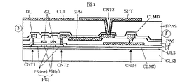
図1〜図5は本発明の一実施例の液晶表示装置に係る画素の平面および断面図である。図2、図3、図4はそれぞれ図1における2−2’、3−3’、4−4’として一点鎖線で示した切断線での断面を示す。図面では切断部を分かりやすくするため、数字を○で囲い切断部を示している。なお図は説明用に要部を記載した物であり、配向膜は図からは省略している図もある。また対向基板側の構成も省略している図もある。以下、順を追って示す。
【0036】
図1は画素の模式平面パターンを示す。隣接するゲート配線GL、隣接するドレイン配線DLに囲まれて1画素を構成する。ゲート配線GLはポリシリコンPSIで構成されたTFTのゲート電極としても作用し、TFTをオンさせる電圧を供給する。ドレイン線はポリシリコンPSIへの電流を供給する、すなわち前記ゲート電圧GLがオン電圧を供給したタイミングで印加された映像電圧(ドレイン電圧)を1画素の液晶容量、保持容量に給電し、結果的に金属画素電極SPM及びこれに連結された透明画素電極SPTの電位が映像電位となる。
【0037】
前記電流の流れはドレイン配線DLから第1のコンタクトホールCNT1を通じてポリシリコンPSIに繋がり、このポリシリコン中の電流は第2のコンタクトホールCNT2を通じて、金属画素電極SPMに流れる。さらに金属画素電極SPMから第3のコンタクトホールCNT3を介して、絶縁膜上の透明画素電極SPTに至る。
【0038】
図1では、DLとPSIのコンタクトホールCNT1の周囲でDLを局部的に太く構成した。これにより、CNT1の接続抵抗の低減と安定したコンタクトが実現する。むろん、コンタクトが正常に出来ればDLの太さは同じでも良い。
【0039】
画素電極と共に液晶容量あるいは保持容量を構成するもう一方の電極の共通電極電位は以下の経路を持ち印加される。隣接するゲート配線間のほぼ中央に配置された横共通電極配線CLMGと、隣接するドレイン配線間のほぼ中央に配置された縦共通電極配線CLMDにまず共通電位が印加される。これらの共通電極配線は画面外部の電源から供給されている。さらに、この横共通電極配線CLMGはゲート配線GLと同一材料で同一工程で形成されている。一方、縦共通電極配線CLMDはドレイン配線DLと同一材料で同一工程で形成されている。
【0040】
本平面構造の1つは、この横共通電極配線CLMGと縦共通電極配線CLMDは第4のコンタクトホールCNT4で互いに結線されている点である。従って、液晶表示装置画面領域から見ると、低抵抗のメッシュ状の共通電極配線が結線された状態で極めて配線遅延が小さくなる。これらの金属で構成された共通電極配線は金属画素電極SPMと横共通電極配線が平面的に重なった面積領域で規定される保持容量に主に電位を給電する役割を果す。保持容量を構成する絶縁膜はゲート配線GLとドレイン配線を絶縁分離する層間絶縁膜である。このように縦共通電極配線CLMDをドレイン配線と同層で形成し、横共通電極配線CLMGをゲート配線と同層で形成し、両者の共通電極配線を各画素で接続することによりゲート配線、ドレイン配線と共通電極配線間の寄生容量を低減でき、マトリクス状の給電の効果も含め、供給する共通電極電位が安定化するため、輝度むら、スメアを大幅に低減した安定した表示が実現する。さらに、該共通電極配線の配置では縦共通電極配線CLMDは同層のドレイン配線と平行方向に、横共通電極配線CLMGはゲート配線と平行方向となる為、同層の電極間での短絡の確率も低減でき、歩留りも高いものとすることが出来る。さらに、ドレイン配線による映像信号は、ドレイン配線が多数のゲート配線を横切って給電される為、容量結合によるゲート配線の影響を含んだものとなる。本実施例では縦共通電極配線CLMDをドレイン配線と同層に形成したことにより、縦方向から供給される共通電位が映像信号に類似した影響をゲート配線から受けたものとなる。この結果、保持容量部に書き込まれる電圧は両者の差電圧となる為、ゲート配線の影響がキャンセルされる方向に働く効果を奏する。このため、さらに表示むらの低減、スメアの低減を図ることが出来る。また図3に明らかなように、横共通電極配線CLMGと縦共通電極配線CLMDを接続するスルーホールCNT4はその上部をPASで保護される為、接続部の信頼性も高いものとすることが出来る。さらにFPASで平坦化できるため、ラビングへの影響も生じない。また横共通電極配線CLMGをゲート配線層で、縦共通電極配線CLMDをドレイン配線層で形成することにより、両者の間のコンタクトホールは無機絶縁膜に形成することが可能となる。このため、コンタクトホールの大きさを低減でき、開口率の一層の向上が実現する。
【0041】
一方、各画素領域には上記メッシュ状に電気的に接続された金属による共通電極配線とは別に、ゲート配線GL及びドレイン配線DL上を低誘電率の絶縁膜を介してその上部に上記配線をシールドするように配置された透明共通電極CLTがあり、隣接する画素間でメッシュ状に構成されている。透明共通電極CLTは画素内へは分岐し、液晶を画素電極SPTと共に駆動する共通電極の役割を果す。透明共通電極CLTは画素内では金属で形成された横共通電極配線CLMGや縦共通電極配線CLMDとは接続されておらず、画面周辺領域で接続結線されている。また、この透明共通電極CLTは、横共通電極配線CLMGや縦共通電極配線CLMDが保持容量を主に充電する配線であるのに対して、液晶容量を充電する役割を果す。IPS液晶表示装置では液晶容量は例えば図1の透明共通電極CLTと透明画素電極SPT間で規定される値となるため、その値は対向する基板面の大部分の領域に形成された電極間で液晶容量を形成するTN液晶表示装置に比べて半分以下という小さい値となる。この結果、透明共通電極CLTの配線抵抗仕様はかなり高い値でも液晶容量に充電することが可能となり、各種透明導電体、すなわちITO(Indium−Tin−Oxide),IZO(Indium−Zinc−Oxide),ITZO(Indium−Tin−Zinc−Oxide),SnO2、In2O3などが使用でき、かつ輝度むらはスメアを抑制した良質の画質が得られる。
【0042】
上記共通電極及び共通電極配線の電位は、フレーム毎に交流化される画素電位のほぼ中点電位が設定される(図14で再度詳細を説明する)。TFTを用いた液晶表示装置の場合、飛び込み電圧による変動を考慮して設定することが望ましい。この画素電極電位と共通電極電位により液晶容量および保持容量が構成されると共に、この電位間の電位差により電界を液晶層内に生じせしめ、前記ドレイン配線DLから供給された映像電圧と前記共通電圧で映像を表示する。図1における主な透過部は2−2’線に沿って設けられた4つの開口部である。
【0043】
以下、各部の構成を断面図を用いて詳細に説明する。図2は図1の2−2’線に沿った断面図であり、隣接するドレイン線DL間の1画素領域を横切る部分である。歪点約670℃の無アルカリTFTガラス基板GLS1上に膜厚50nmのSi3N4膜と膜厚120nmのSiO2膜からなる下地絶縁膜ULSが形成されている。下地絶縁膜ULSはTFTガラス基板GLS1からのNa等の不純物の拡散を防止する役割を持つ。下地絶縁膜ULS上には、SiO2からなるゲート絶縁膜GIが成膜されている。
【0044】
上記を覆うようにSiO2からなる層間絶縁膜ILIが形成され。層間絶縁膜ILI上にはTi/Al/Tiのように3層金属膜よりなるドレイン配線DLが形成されている。上記ドレイン配線DLと同一材料、同一工程で形成された金属画素電極SPMは、図1においてTFTの第2のコンタクトホールCNT2から画素電位を給電する電極である。また、同層上には平行して、前記ドレイン配線DLと同一材料、同一工程で形成された縦共通電極配線CLMD配置されてあり、これは保持容量に対して共通電位を給電する役割を果す。
【0045】
その上層には膜厚200nmのSi3N4からなる保護絶縁膜PASと膜厚2μmのアクリル系樹脂を主成分とする有機保護膜FPASにより被覆されている。有機保護膜FPAS上では、まずドレイン配線DLの幅より広く、インジウム−スズ酸化物(ITO)よりなる透明共通電極CLTが形成されている。同一工程、同一材料で作製されたITOからなる透明画素電極SPTも前記有機絶縁膜FPAS上に形成されている。
【0046】
上記説明中、配線材料は特に限定する物ではない。
【0047】
主な透過領域は(1)ドレイン線DL上の透明共通電極CLTと透明画素電極SPT間、(2)前記透明画素電極SPTと図1の平面図において縦共通電極配線CLMDを被覆するように配置され、ゲート配線GL上側から上下に延びた透明共通電極配線CLTの間、(3)前記透明共通電極CLTと透明画素電極SPTとの間、(4)前記透明画素電極SPTとドレイン配線DL上の透明共通電極CPTの間の4つの領域である。上記透明画素電極SPT、透明共通電極CPTが液晶を駆動する電極である。
【0048】
一方、液晶LCを封止する対向の基板はカラーフィルタ(CF)基板GLS2である。CFガラス基板GLS2は、液晶側に色表示を行う顔料を分散した有機膜材料から構成された色フィルタ(FIL)がその画素毎に割り当てられた色に応じて、青(B)、赤(R)、緑(G)の透過光を表現する色フィルタ(赤ではFIL(R))となっている。その内側には有機材料からなるオーバコート膜OC膜が形成されている。OC膜は無くても良いが、平坦性を向上する目的ではあるほうが望ましい。CF基板GLS2及びTFT基板GLS1の液晶LCに対して接している面には配向膜OLIが印刷されて所定のラビングが施され、初期配向方向を制御している。また上記、CFガラス基板GLS2及びTFTガラス基板GLS1の外側の面にはそれぞれ偏光板POLが貼られる。この偏光板は互いのガラス基板間で偏向軸が直交するいわゆるクロスニコル状態が形成されている。
【0049】
ラビング方向と偏光板の角度の関係を図16に示す。偏光軸の一方PD2はGLと同方向に、他方PD1はGLと直交方向としている。またラビング方向RDは上下基板ともGLと直交する方向とした。これによりノーマリーブラックモードの配置となり、さらに図1のような屈曲形状の画素パターンによりマルチドメイン化を行っている。むろん、非マルチドメインの場合も本願の範疇に含むものであり、その場合でも偏光板配置がクロスニコルになるようにすることが必要である。
【0050】
本断面のCF基板GLS2には、いはゆる、ブラックマトリクスBMが形成されていない。カラーフィルタFILの色のつなぎあわせは、ドレイン配線DLを被覆するように配置された透明共通電極配線CLT上で行う。
【0051】
本断面構造の特徴の1つは、有機絶縁膜FPAS上の透明画素電極SPT及び透明共通電極CPTにより液晶LCに対して、1画素が少なくとも4分割の開口(主な透過領域)を持つことである。
【0052】
また別の特徴は、有機保護膜FPAS上に、液晶表示電圧を印加するように間隔を開けて配置された所定の幅を有する透明画素電極SPTと透明共通電極CLTの下部に、有機絶縁膜FAPS及び保護膜PASの積層絶縁膜を挟んで金属画素電極SPM、縦共通電極配線CLMD及びドレイン配線DLが配置されていることである。それぞれの透明電極幅は以下のように設定される。
【0053】
ドレイン配線DLを被覆する透明共通電極配線CLT幅はドレイン配線幅の少なくとも2倍以上必要である、これは、IPS液晶表示装置が基本的に液晶に共通電極電位と画素電位以外の電界が加わるとスメアやドメインが生じるため、そのシールドが必要なためである。一方、金属画素電極SPMと縦共通電極配線CLMD上の透明電極SPT及びCLTの幅は、これらが下部の金属電極と同電位であるため、金属電極であるSPM、CLMDの幅に制約されない。但し、ポジ型の液晶材料を用いたIPS液晶表示装置では透明電極上であっても光が透過しない。これは幅の広い電極上では横電界がかからず液晶分子が回転しないためである。これに対し、透明電極の端部からその幅の内部に向かって1.5μmまでの領域はフリンジの横電界がかかり透過する。以上の点で、金属画素電極SPM及び縦共通電極配線の幅は基本的に、それぞれその上部の透明画素電極SPT及び透明共通電極配線CLTと同じ幅かそれより狭く設定される。また、縦共通電極配線CLMDはその配線材料がドレイン配線DLと同じで基本的に低抵抗のTi/Al/Ti配線であり、その幅はプロセスルールで決まる最小値を設定しても配線遅延が小さくでき、開口率を低下させることはない特徴がある。特に、本実施例では、液晶駆動に不可欠な透明電極配線CLT下部に配置されており、新たに開口率を低下させないことも特徴の1つになっている。
【0054】
図3は図1の3−3’の線に沿った断面図である。本断面図は図1の平面図においてドレイン配線DL〜第1のコンタクトホールCNT1〜TFTのポリシリコン層PSI〜第2のコンタクトホールCNT2〜横共通電極配線CLMG上に層間絶縁膜ILIを介して乗り越え配置された金属画素電極SPM〜第3のコンタクトホールCNT3〜横共通電極配線CLMGと縦共通電極配線CLMDを接続する第4のコンタクトホールCNT4の断面を示す。図3の断面図の左側はTFTの断面である。ドレイン配線DL、金属画素電極SPMをいわゆるドレイン電極、ソース電極とし、ゲート配線GLをゲート電極として、ゲート絶縁膜GIを有するいわゆるMOS型TFTである。ULS上にp−Si層があり、ドレイン配線DL及び金属画素電極SPMはゲート絶縁膜GI及び層間絶縁膜ILIに開けられた第1のコンタクトホールCNT1及び第2のコンタクトホールCNT2を各々通じて、低温ポリシリコンPSIのリンを不純物としてドープされた高濃度n型層PSI(n+)に接続されている。該高濃度n型層PSI(n+)は導電性が高く、擬似的に配線部として働く。一方GL下のPSIはボロンを不純物としてドープされたp型層PSI(p)となっており、いわゆる半導体層として働き、GLにON電位で導通状態、OFF電位で非導通状態となるスイッチング動作を示す。ゲート配線GLにオン電圧が印加された場合、ゲート配線GL下部でゲート絶縁膜GI下部であり、ボロンを不純物としてドープされたp型層PSI(p)のゲート絶縁膜GI界面のポテンシャルが反転してチャネル層が形成され、n型化されTFTにオン電流が流れ、結果的に金属画素電極SPMへ電流が流れ液晶容量及び保持容量が充電される。保持容量Cstgは同図ように横共通電極配線CLMGを一方の電極、絶縁膜として層間絶縁膜ILI、他方の電極を金属画素電極SPMとして形成されている。保持容量Cstgは、同図のTFTのポリシリコンPSIに対してTFTガラス基板GLS1側からの表示のバックライトによる光照射で発生する電子、正孔のペヤで増加するリーク電流に対して液晶容量で決まる画像表示期間(保持期間)中の電位を保つために設定されている。この値を大きく設定できれば、表示画面上の均一性を極めて良好に保つことができる。
【0055】
図4は図1の4−4’の線に沿った断面図である。本断面図は主に、ゲート配線GLとTFTの低温ポリシリコンPSI及びこれらを有機保護膜を介して被覆している透明共通電極配線CLTから透過領域に至る断面構造を表す。
【0056】
図4の断面構造は左手側にゲート配線GL、右手側が透過領域である。ゲート配線GL及び低温ポリシリコンPSIは保護膜PAS及び有機保護膜FPAS上に配置された透明共通電極CLTで被覆されている。これはゲート配線GLの電位が透明共通電極CLTおよび透明画素電極SPTで挟まれた透過領域に、ゲート配線GLの電気力線が漏れ、表示の誤動作を起こさないようにするためである。
【0057】
本構造の特徴は上記ゲート配線及び低温ポリシリコン層を被覆するように配置された透明共通電極配線CLTが透明電極ながら極めて良質なブラックマトリクスBMの効果を示す点にある。図2に示すように、液晶を駆動させる電界Eは透明共通電極配線CLTと透明画素電極SPTの横電界である。IPS型液晶表示装置では、この横電界で液晶分子LCを回転させ直交する偏光板POLに対して透過率を変える。無電界あるいは横方向電界が小さい状態では偏光板がクロスニコル配置されているため、黒表示となる。電界が印加されると楕円偏光の透過が発生し、電界に応じて透過する。従って、無電界や横方向電界が小さい領域では、透明共通電極CLTがITOのような透明電極で形成された場合においてもTFTガラス基板GLS1側からのバックライト光は透過せず、観察者側であるCF基板GLS2から見ても良好な黒状態となる。一方、電圧印加状態では、透明電極の端部から電極内部へ約1.5μmの領域(例えばGL上のCLTの場合での領域の例を図4にWTとして示す)では、フリンジ状態の横電界成分があり、透過に寄与する。
【0058】
従って、TFTガラス基板GLS1側からのバックライト光の画像に対しては、図1の平面構造において、少なくとも低温ポリシリコンPSIを含むTFTとゲート配線GLを覆うように幅広く設定された透明共通電極CLTは、人間の目視時に、各画素の輪郭を明瞭にし、画像をくっきりとさせるBM同様の働きをする。図4において、その透明共通電極CLT上のWN領域、すなわち透明電極単体が存在し、かつ透明電極端部から1.5μm以上内側の領域は横方向電界成分がほとんどなく、液晶層透過中に光の偏向状態は影響を受けないため、最終的にCF基板上の偏光板POLで遮光される。例えば、低温ポリシリコンPSIが赤色着色してみえるはずが、完全な黒表示状態のBMに見える。ゲート配線GLの領域WRで,はこの金属で完全に遮光されるので、電界に係わらず黒状態になる。
【0059】
図4の断面図で示す通り、本実施例構造ではCF基板GLS2には従来のBMが形成されていない。このため本実施例構造を用いたIPS型の液晶表示装置はBM層形成工程が不要となるため、コスト低減が実現できる。外光に対しては、前記透明共通電極CLTは、極めて良好な反射の少ないBMの役割を果す。これは透明電極を遮光層として用いるからこその効果であり、かつその遮光層が観察側基板と対向する基板にあることで、一層反射が低減する。透明共通電極CLTのWNの領域では外光はCLT自身の吸収、保護膜PAS、有機保護膜FPAS、などで吸収されるが、反射率の高い金属層がないため観察者側への反射は少ない。一方、ゲート配線GL上はその材料はMoWであり、例えば、Alに比べては小さいが若干の反射は存在するが、上層の保護膜がPASなどを2回通過することとクロスニコル状態の偏光板POLの効果もあり小さい反射に止まる。このように、透明共通電極CLTをブラックマトリクスBMとして使用した場合、極めて反射の少ないBMが形成できる。さらに、CF基板にBMを形成する必要がなくなるため、上下基板の合わせ裕度が拡大し、生産性の向上が実現する。また合わせずれを見越した設計が不要となるため、従来BMとして遮光が必要な領域より合わせ裕度を見越して余分にBMで遮光されていた領域が透過領域となるため、開口率の向上が実現する。さらに、透明電極端部での遮光領域が黒表示時は電極上全領域、白表示時は電極端から1.5μmまでは透過領域となるため、くっきりと画像を表示する必要がある黒表示状態と、明るい表示が必要な白表示状態とで、動的かつ自動的に遮光領域が変化し、黒表示では遮光領域が広く、白表示では遮光領域が狭くなるまさに理想的なBMとして透明電極による遮光層は働く。これにより、画像のくっきりさの向上、コントラストの向上、及び輝度の向上という一見相反する事象を両立することが可能となった。
【0060】
次に、図3に示すようなNMOS型TFTの製造工程を図5〜図9及び図3を用いて説明する。
【0061】
厚さ0.7mm、サイズ730mm×920mmの歪点約670℃の無アルカリTFTガラス基板GLS1を洗浄後、SiH4とNH3とN2の混合ガスを用いたプラズマCVD法により膜厚50nmのSi3N4膜、続いて、テトラエトキシシランとO2の混合ガスを用いたプラズマCVD法により、膜厚120nmのSiO2膜の積層の下地絶縁膜ULSを形成する。本絶縁膜ULSは多結晶シリコン膜へのTFTガラス基板GLS1からのNa拡散を防止するためである。Si3N4、SiO2ともに形成温度は400℃である。なお、本願では半導体層として多結晶シリコンで代表するが、巨大結晶シリコン、連続粒界シリコン、アモルファスシリコンでもよい。
【0062】
次に、上にSiH4、Arの混合ガスを用いたプラズマCVD法によりほぼ真性(イントリンシック)の水素化非晶質シリコン膜を50nm形成する。成膜温度は400℃で、成膜直後水素量は約5at%である。次に基板を450℃で約30分アニールすることにより、水素化非晶質シリコン膜中の水素を放出させる。アニ−ル後の水素量は約1at%である。
【0063】
次に、波長308nmのエキシマレーザ光LASERを前記非晶質シリコン膜にフルエンス400mJ/cm2、で照射し、非晶質シリコン膜を溶融再結晶化させて、ほぼ真性の多結晶シリコン膜を得る。この時レーザビームは幅0.3mm、長さ200mmの細線状の形状であり、ビームの長手方向とほぼ垂直な方向に基板を10μmピッチで移動しながら照射した。照射時は窒素雰囲気とした。
【0064】
通常のホトリソグラフィ法により所定のレジストパターンを多結晶シリコン膜上に形成しCF4とO2の混合ガスを用いたリアクティブイオンエッチング法により多結晶シリコン膜PSIを所定の形状に加工する(図5)。
【0065】
次に、テトラエトキシシランと酸素の混合ガスを用いたプラズマCVD法により膜厚100nmのSiO2を形成しゲート絶縁膜GIを得る。この時のテトラエトキシシランとO2の混合比は1:50、形成温度は400℃である。引き続きイオン注入法によりよりBイオンを加速電圧33KeV、ドーズ量1E12(cm−2)で打ちこみ、n型TFTのチャネル領域のポリシリコン膜PSI(p)を形成する。
【0066】
次にスパッタリング法により、金属配線、例えばMoあるいはMoW膜を200nm形成後、通常のホトリソグラフィ法により所定のレジストパターンをMo膜上に形成し、混酸を用いたウェットエッチング法によりMo膜を所定の形状に加工し走査配線GLおよび第2の横共通電極配線CLMGを得る。
【0067】
エッチングに用いたレジストパターンを残したまま、イオン注入法によりよりPイオンを加速電圧60KeV、ドーズ量1E15(cm−2)で打ちこみ、n型TFTのソース、ドレイン領域PSI(n+)を形成する(図6)。上記でn型TFTのソース、ドレインがn+型の低温ポリシリコン膜PSI(n+)及びp型のチャネル領域のポリシリコン膜PSI(p)ができあがるが、以下のようにp型とn+型の間にPイオン濃度がn+型より少ないn型のLDD領域を作り、TFTのリーク電流を低減することができる(図示していない)。すなわち、エッチングに用いたレジストパターンを除去後、再度イオン注入法によりPイオンを加速電圧65KeV、ドーズ量2E13(cm−2)で打ちこみ、n型TFTのLDD領域を形成する。LDD領域の長さはMoをウェットエッチングしたときのサイドエッチング量で定められる。本実施例の場合約0.8μmである。この長さはMoのオーバーエッチング時間を変化させることで制御できる。
【0068】
次に、基板にエキシマランプまたはメタルハライドランプの光を照射するラピッドサーマルアニール(RAT)法により打ち込んだ不純物を活性化する。エキシマランプまたはメタルハライドランプ等の紫外光を多く含む光を用いてアニールすることにより、多結晶シリコン層PSIのみを選択的に加熱でき、ガラス基板が加熱されることによるダメージを回避できる。不純物の活性化は、基板収縮や曲がり変形等が問題にならない範囲で、450℃程度以上の温度での熱処理によっても可能である(図6)。
【0069】
次に、テトラエトキシシランと酸素の混合ガスを用いたプラズマCVD法により膜厚500nmのSiO2を形成し層間絶縁膜ILIを得る。この時のテトラエトキシシランとO2の混合比は1:5、形成温度は350℃である。
【0070】
次に、所定のレジストパターンを形成後、混酸を用いたウェットエッチング法により、前記層間絶縁膜に第1のコンタクトスルーホールCNT1、第2のコンタクトホールCNT2及び図1の平面図の第4のコンタクトホールCNT4を開孔する(図7)。
【0071】
続いて、スパッタリング法により、Tiを50nm、Al−Si合金を500nm、Tiを50nmを順次積層形成した後に所定のレジストパターンを形成し、その後BCl3とCl2の混合ガスを用いたリアクティブイオンエッチング法により一括エッチングし、ドレイン配線DL、金属画素電極SPM、縦共通電極配線CLMDを得る(図8)。
【0072】
SiH4とNH3とN2の混合ガスを用いたプラズマCVD法により膜厚300nmのSi3N4膜である保護膜PASを形成し、さらに、スピン塗布法によりアクリル系感光性樹脂を約3.5μmの膜厚で塗布し、所定のマスクを用いて露光、現像して前記アクリル系樹脂にスルーホールを形成する。次に230℃で20分ベークすることで、アクリル樹脂を焼成し、膜厚2.0μmの平坦化有機保護膜FPASを得る。続いて、前記有機保護膜FPASに設けたスルーホールパターンをマスクとして下層のSi3N4膜をCF4を用いたリアクティブイオンエッチング法により加工し、Si3N4膜に第3のコンタクトホールCNT3を形成する(図9)。
【0073】
このように有機保護膜FPASをマスクとして用いて下層の絶縁膜を加工することにより、一回のホトリソグラフィ工程で2層の膜をパターニングでき、工程を簡略化できる。
【0074】
最後にスパッタリング法によりITO膜等の透明導電膜を70nm形成し、混酸を用いたウェットエッチングにより所定の形状に加工して透明共通電極配線CLTおよび透明画素電極SPTを形成しアクティブマトリクス基板が完成する(図3)。以上6回のホトリソグラフィ工程で多結晶シリコンTFTが形成される。
【0075】
次に液晶パネルの概観の平面構造について説明する。図10は上下のガラス基板GLS1、GLS2を含む表示パネルのマトリクス(AR)周辺の要部平面を示す図である。このパネルの製造では、小さいサイズであればスループット向上のため1枚のガラス基板で複数個分のデバイスを同時に加工してから分割し、大きいサイズであれば製造設備の共用のためどの品種でも標準化された大きさのガラス基板を加工してから各品種に合ったサイズに小さくし、いずれの場合も一通りの工程を経てからガラスを切断する。
【0076】
図10は後者の例を示すもので、上下基板GLS1、GLS2の切断後を表している。いずれの場合も、完成状態では外部接続端子群Tg、Tdが存在する部分(図で上辺)はそれらを露出するように上側基板GLS2の大きさが下側基板GLS1よりも内側に制限されている。端子群Tg、Tdはそれぞれ後述するTFTガラス基板GLS1上で表示部ARの左右に配置された低温ポリシリコンTFTの走査回路GSCLへ供給する電源及びタイミングデータに関する接続端子、表示領域ARの上部でTFTガラス基板GLS1上に低温ポリシリコンTFTの映像信号回路DDCへの映像データあるいは電源データを供給するため端子Tdである。引出配線部を集積回路チップCHIが搭載されたテープキャリアパッケージTCP(図11)の単位に複数本まとめて名付けたものである。各群のマトリクス部から映像信号回路DDCを経て外部接続端子部に至るまでの引出配線は、両端に近づくにつれ傾斜している。これは、パッケージTCPの配列ピッチ及び各パッケージTCPにおける接続端子ピッチに表示パネルの映像信号端子Tdを合わせるためである。
【0077】
透明ガラス基板GLS1、GLS2の間にはその縁に沿って、液晶封入口INJを除き、液晶LCを封止するようにシールパターンSLが形成される。シール材は例えばエポキシ樹脂から成る。
【0078】
図2の断面構造で示した配向膜ORI層は、一例としてシールパターンSLの内側に形成される。液晶LCは液晶分子の向きを設定する下部配向膜ORIと上部配向膜ORIとの間でシールパターンSLで仕切られた領域に封入されている。
【0079】
この液晶表示装置は、下部透明TFTガラス基板GLS1側、上部透明CFガラス基板GLS2側で別個に種々の層を積み重ね、シールパターンSLを基板GLS2側に形成し、下部透明ガラス基板SUB1と上部透明ガラス基板GLS2とを重ね合わせ、シール材SLの開口部INJから液晶LCを注入し、注入口INJをエポキシ樹脂などで封止し、上下基板を切断することによって組み立てられる。
【0080】
図11は、図10に示した表示パネルに映像信号駆動ICを搭載したTCPとTFT基板GLS1上に低温ポリシリコンTFTで形成した信号回路DDCとの接続及びTFT基板GLS1に低温ポリシリコンTFTで形成した走査回路GSCLと外部とを接続した状態を示す上面図である。
【0081】
TCPはテープキャリアパッケージであり、駆動用ICチップがテープ・オートメイティド・ボンディング法により実装されたものである。PCB1は上記TCPやコントロールICであるTCON、その他電源用のアンプ、抵抗、コンデンサ等が実装された駆動回路基板である。CJはパソコンなどからの信号や電源を導入するコネクタ接続部分である。
【0082】
図12はテープキャリアパッケージTCPを液晶表示パネルの、信号回路用端子Tdに接続した状態を示す要部断面図である。テープキャリアパッケージTCPは異方性導電膜ACFによって液晶表示パネル接続される。TCPは電気的にはその出力端子がパネル側の接続端子Tdと接続され、TFTの保護膜PASおよび有機保護膜FPASの開口部を覆うように形成され、かつ透明共通電極CLTと同一工程で形成された透明電極ITOと接続されている。シールパターンSLの外側の上下ガラス基板の隙間は洗浄後エポキシ樹脂EPX等により保護され、TCPと上側CF基板GLS2の間には更にシリコン樹脂が充填され保護が多重化されている(図示していない)。また上下のガラス基板GLS2、GLS1の液晶LCに対するギャップは有機膜で形成された支柱SPCあるいはファイバでその高さが決定されている。
【0083】
表示マトリクス部の等価回路とその周辺回路の結線図を図13に示す。図中、DLはドレイン線を意味しDL1、DL2、DL3とその数字が画面左からの画面内のドレイン配線(映像信号線)を意味する、添字R、GおよびBがそれぞれ赤、緑および青画素に対応して付加されている。GLはゲート配線GLを意味し、GL1、GL2、とその数字が画面上部からの画面内のゲート線を意味する。添字1、2、は走査タイミングの順序に従って付加されている。CLXは横共通電極配線CLMGを意味し、CLX1、CLX2とその数字が画面上部からの画面内の共通電極配線を意味する。一方、CLYは縦共通電極配線CLMDを意味し、CLY1、CLY2とその数字が画面上部からの画面内の共通電極配線を意味する。
【0084】
ゲート配線GL(添字省略)はガラス基板上の走査回路GSCLに繋がれ、その走査回路への電源あるいはタイミング信号はガラス基板外部のPCB上に形成された電源及びタイミング回路SCCから供給される。 上記において低温ポリシリコンTFTで構成されたガラス基板上の走査回路は、冗長性を高めるために1本のゲート線(走査線)に対して左右の両側から給電されているが、画面サイズなどに応じて片側から給電しても良い。
【0085】
一方、ドレイン配線DLへの給電はガラス基板上の低温ポリシリコンTFTで構成された信号回路DDCから給電される。信号回路DDCはガラス基板の映像信号回路ICで構成された回路よりの映像データをR、G、Bの色データに応じて分配する機能を持つ。従って、ガラス基板上の信号回路からの接続端子数は画面内のドレイン配線数の三分の一である。
また、共通電極配線は、本実施例では、金属で構成された横共通電極配線CLX、縦共通電極配線CLY、と透明共通電極がある。横共通電極配線と縦共通配線は、図1で示したように、画素内で結線されマトリクス状の金属配線となっている。横共通電極配線CLXは、画面の左右に引き出され、まとめてインピーダンスの低い共通電極母線CLBに結線され、電源及びタイミング回路ICのSCCに結線される。縦共通電極配線CLYは下部に引き出され、インピーダンスの低い共通電極母線CLBに結線され、同じく電源回路SCCに至る。透明共通電極は、図1に示したように、画面内では前記横共通電極配線、縦共通電極配線と結線されず、画面外周で、左右方向では横共通電極配線、下部では縦共通電極配線と結線され、共通電極母線CLBに結線され同様に外部電源SCCにつながれる。図13では図示していないが、マトリクス状に構成されている。この共通電極は、画面内の画素のコモン電位を与える。
【0086】
画面内の低温ポリシリコンTFTは、n型のTFTであり、ゲート配線GLにゲート電圧を印加し、そのタイミングでドレイン線DLに給電されたドレイン電圧(データ)を共通電極配線との間の液晶容量Clcに給電することにより表示を行う。液晶容量Clcの電位を表示期間中に維持する能力を向上するために、横共通電極配線CLMGと図3に示すように金属画素電極SPMとの間に保持容量Cstgを形成する。CCはドレイン配線DLの断線を検査する低温ポリシリコンTFTで形成した検査回路であり、CPADは検査端子である。
【0087】
図14に本発明の液晶表示装置の駆動波形を示す。共通電極電圧Vcomを直流電圧とした場合の例を示す。ゲート電圧Vgは1ゲート線毎に順次走査し、ドレイン電位Vdに対して、画素の低温ポリシリコンTFTのしきい電圧を更に加算した電圧が印加された際に画素TFTがオン状態になり、図13に示した液晶容量Clcに充電される。 上記共通電極電圧Vcom、ゲート電圧Vg、ドレイン電圧Vdはそれぞれ図13の横共通電極配線CLX,縦共通電極配線CLY、図1に示した透明共通電極CLT、ゲート配線GL、ドレイン配線DLに印加される。本実施例では、ドレイン電圧Vdは、例えば、ノーマルブラックモードでの液晶表示で白表示を行う場合を示しており、ゲート線は1ライン毎に選択され、そのライン毎に共通電極電圧Vcomに対してプラス、マイナスの極性反転される。画素電位VpはTFTを通じて液晶容量Clcに充電されるが、奇数、偶数フレームで共通電極電位Vcomに対して反転される。特定のアドレスのTFTのゲート配線GLに対して、ゲート配線が選択されVgがVdより大きくなると液晶容量Clcに画像に対応する電位が充電されるが、上記のように次ぎのフレームになり、共通電極電位Vcomに対して反転されたVdが印加されるまで液晶容量Clcの電位は保持されなければならない。この保持率はTFTのオフ(リーク)電流が大きくなると低下する。これを防止するには、図13の等価回路の保持容量Cstgを大きく設定する必要がある。この保持容量Cstg大きくした場合、共通電極配線の寄生容量が大きい場合、配線遅延が増大し、輝度むら、スメア、さらには残像やフリッカの画面内均一性が保てなくなるが、図1、図3の平面及び断面構造に示すように、金属材料の横共通電極配線CLMGと縦共通電極配線CLMDを画面内で結線し、マトリクス状にして抵抗を小さくする構成としている。一方、透明共通電極CLTは画面内では有機絶縁膜状に画素間を繋ぐように結線され、画面内ではCLTと金属共通電極配線CLMG、CLMDは直接は結線されていない。しかしCLTの役割は影響容量の充電のみであり、前述のように抵抗の比較的高い材料でも適用可能である。さらに画面外部で低インピーダンスの図13の共通電極母線CLBに接続され、低抵抗化されている。これらの効果により、本願では保持容量Cstgを増加させた場合でも画面の画質均一性を高めることができる。
【0088】
図15は、液晶表示モジュールMDLの各構成部品を示す分解斜視図である。SHDは金属板から成る枠状のシールドケース(メタルフレーム)、LCWはその表示窓、PNLは液晶表示パネル、SPBは光拡散板、LCBは導光体、RMは反射板、BLはバックライト蛍光管、LCAはバックライトケースであり、図に示すような上下の配置関係で各部材が積み重ねられてモジュールMDLが組み立てられる。
【0089】
モジュールMDLは、シールドケースSHDに設けられた爪とフックによって全体が固定されるようになっている。バックライトケースLCAはバックライト蛍光管BL、光拡散板SPB光拡散板、導光体LCB、反射板RMを収納する形状になっており、導光体LCBの側面に配置されたバックライト蛍光管BLの光を、導光体LCB、反射板RM、光拡散板SPBにより表示面で一様なバックライトにし、液晶表示パネルPNL側に出射する。バックライト蛍光管BLにはインバータ回路基板PCB2が接続されており、バックライト蛍光管BLの電源となっている。
【0090】
(実施例2)
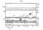
図17は本発明の第2の実施例を示す画素の平面図であり、図18はその図17における18−18’として一点鎖線で示した切断線での断面を示す。図面では切断部を分かりやすくするため、数字を○で囲い切断部を示している。
【0091】
図17は実施例1と同様にドレイン配線DLを横切る方向に主な透過部を4つもつIPS方式の画素パターンである。構成は実施例1に近いが大きな特徴は金属で構成された共通電極配線は、縦共通電極配線CLMDのみが配線されている点であり、図1で配置されていた横方向共通電極配線が除去されている。従って、保持容量形成に新たな構成を用いている。さらに、該構造により、開口率が実施例1に比べて向上することが出来た。
【0092】
保持容量Cstgは以下のような構成となっている。まず、ゲート配線GLと同一工程、材料で構成された保持容量電極STMを島状に加工する。これを第4のコンタクトホールCNT4を介して縦共通電極配線CLMDと結線する。一方、低温ポリシリコンPSIで構成されたTFTの第2のコンタクトホールCNT2から延びた金属画素電極SPMは、保持容量電極STM上に延びる。この金属画素電極SPMと保持容量電極STMは層間絶縁膜を介してその重なる面積部分が保持容量を構成する。透明画素電極SPTは第3のコンタクトホールCNT3を介して金属画素電極SPMと結線され、画素電位が液晶に給電させる。一方、透明共通電極配線CLTは、画面内では縦共通電極配線CLMDとは結線されないが、画面領域外で結線され共通電位を液晶に給電する。
【0093】
上記の構成により、新たに、2つの効果が得られる。第1は、図17の画素の平面図の4つの透過領域の内、ドレイン配線DLを被覆する透明電極配線CLTとその画素内の内側の透明画素電極SPTで規定される新たな開口部が、実施例1の図1の横共通電極配線が除去されることにより、形成されることである(図17のLL、LRで規定される領域)。これにより、明るいIPS型の液晶表示装置が提供できる。第2は、ドレイン配線DLと交差する横共通電極配線CLMGが除去されることで、ドレイン配線DLの寄生容量が低減される。これにより、図13のドレイン分割回路DDCの内蔵回路の分割数を増やすことができ、図11に示したTCPで構成された部材数を少なくできコストが低減できる。
【0094】
図17の18−18’切断線における断面図が図18である。映像信号となるドレイン電圧は、ドレイン配線DLから第1のコンタクトホールCNT1を介して低温ポリシリコンPSIで伝えられる。ゲート電圧GLにオン電圧が印加させるとMOS型TFTが動作し、映像電圧が、第2のコンタクトホールCNT2を介して接続された金属画素電極SPMへ伝えられ、最終的に第3のコンタクトホールを介して接続された透明画素電極SPTに伝えられ、液晶容量の一方の電位の画素電位となる。液晶を駆動する他方の電位である共通電圧は、透明共通電極配線CLTに印加される。図17のLRで示した新たな開口部は、この透明画素電極SPTと透明共通電極配線CLTに印加される横電界で新たな透過領域となり、明るい液晶表示装置が提供できる。
【0095】
さらに、本図でも明らかなように、CF基板にはブラックマトリクスは形成されておらず、低温ポリシリコンで形成されたTFTおよびゲート配線GLは有機保護膜FPAS上に配置された透明共通電極配線で覆われ、透明電極であるが、横電界がかからない領域を形成し、良好なブラックマトリクスの役目を果している。
【0096】
さらに本実施例では除去する共通電極配線を横共通電極配線CLMGとしたため、実施例1で説明した縦共通電極配線CLMDがドレイン配線DLと同層で、かつゲート配線GLを横切るために得られる保持容量に対してのゲート電位のキャンセル効果はそのまま奏することが出来る。
【0097】
(実施例3)
図19は本発明の第3の実施例を示す画素の平面図であり、図20は図19における20−20’として一点鎖線で示した切断線での断面を示す。図面では切断部を分かりやすくするため、数字を○で囲い切断部を示している。
【0098】
図19は実施例2と同様にドレイン配線DLを横切る方向に主な透過部を4つもつIPS方式の画素パターンである。構成は実施例2に近いが大きな特徴は、保持容量の下部電極がポリシリコンPSIで構成されて、このポリシリコンPSIは第5のコンタクトホールを介して縦共通電極配線CLMDと接続されて点である。これに伴い、保持容量を構成する絶縁膜のショート欠陥率が低減し、歩留りを一層向上した液晶表示装置となっている。
【0099】
保持容量Cstgは以下のような構成となっている。まず、薄膜トランジスタの低温ポリシリコンPSIを島状に加工する。これを第5のコンタクトホールCNT5を介して縦共通電極配線CLMDと結線する。一方、低温ポリシリコンPSIで構成されたTFTの第2のコンタクトホールCNT2から延びた金属画素電極SPMは、保持容量の下部電極を構成する低温ポリシリコンPSI上に延びる。この金属画素電極SPMと保持容量の下部電極を構成する低温ポリシリコンPSIはゲート絶縁膜と層間絶縁膜を介してその重なる面積部分が保持容量を構成する。透明画素電極SPTは第3のコンタクトホールCNT3を介して金属画素電極SPMと結線され、画素電位が液晶に給電させる。一方、透明共通電極CLTは、画面内では縦共通電極配線CLMDとは結線されないが、画面領域外で結線され共通電位を液晶に給電する。
【0100】
図19の20−20’切断線における断面図が図20である。映像信号となるドレイン電圧は、ドレイン配線DLから第1のコンタクトホールCNT1を介して低温ポリシリコンPSIで伝えられる。ゲート電圧GLにオン電圧が印加させるとMOS型TFTが動作し、映像電圧が、第2のコンタクトホールCNT2を介して接続された金属画素電極SPMへ伝えられ、最終的に第3のコンタクトホールを介して接続された透明画素電極SPTに伝えられ、液晶容量の一方の電位の画素電位となる。液晶を駆動する他方の電位である共通電圧は、透明共通電極配線CLTに印加される。図19のLRで示した新たな開口部は、この透明画素電極SPTと透明共通電極配線CLTに印加される横電界で新たな透過領域となり、明るい液晶表示装置が提供できる。
【0101】
保持容量Cstgの下部電極は低温ポリシリコンPSI(n+)で構成されているため、その絶縁膜はゲート絶縁膜GIと層間絶縁膜ILIの積層膜となるため、その絶縁耐圧は実施例3の保持容量の層間絶縁膜ILIの単層膜に比べて高い。これにより、ショート不良による点欠陥の少ないIPS型の液晶表示装置が提供できる。
【0102】
(実施例4)
図21は本発明の第4の実施例における画素の平面図、図22および図23は図21の平面図における21−21’線、22−22’線における断面構造である。
【0103】
図21の画素の平面パターンは、1画素のサイズの大きく、しかも画面サイズの大きい液晶テレビにて開口率を向上する構成を提供する。図21は横方向に10個の透過領域を有し、その10分割された櫛歯電極間の寸法はL1、L2、L3、L4、L5、L6、L7、L8、L9、L10と表記されている。各櫛歯電極間の間隔Lは、実施例1の図1とおおよそ同じである。本実施例は、大画面の高輝度タイプの液晶テレビに対して好適なIPS液晶表示装置での画素パターンである。低温ポリシリコンPSIを用いたTFTでは、図3に示すようにバックライトはTFTガラス基板側に配置されており、その光は直接低温ポリシリコンPSIに照射される。そのため、光照射リーク電流が増加して、画素電位が低下する問題がある。これに対処するには、1画素の保持容量を大きくして、さらにそれに伴い増加する共通電極配線の配線遅延を低減することが必要である。
【0104】
図21の画素では隣り合うドレイン配線DLとゲート配線GLに囲まれた1画素領域で、ドレイン配線DLと同一工程、材料で構成された縦共通電極配線CLMDはドレイン配線とほぼ平行して、透明共通電極配線CLTの下部に配置されている。縦共通電極配線CLMDは共通電位が印加されているので、その断面構造に対しては、図22に示すように、透明共通電極配線CLT下部に配置されなければならない。透明画素電極SPT下部に配置されると、画素電極SPTと透明共通電極配線CLTで規定される映像データを乱してしまうためである。従って、縦共通電極配線CLMDは、ドレイン配線DLから、1つの目の透明画素電極SPTより少なくとも1つの櫛歯間隔(図21におけるL9)を経て、その内側に平面的に配置させる必要がある。また、縦共通電極配線CLMDとドレイン配線は製造プロセス上は、同一工程、材料で構成させるので、製造工程中のゴミによりショートしやすく、ショートした場合は線上の欠陥となる。その点で、ドレイン配線DLより、画素内側に少なくとも2つの開口部(図21のL9、L10)を経て配置されるのは歩留り上も有利である。
【0105】
前記縦共通電極配線CLMDは第4のコンタクトホールを介して、横共通電極配線CLMGと接続され、画面上において金属のマトリクス配線となり、大きな保持容量を形成した場合でも配線遅延が少なく均一の画面表示が実現できている。保持容量は、図21の平面図においては、低温ポリシコンPSIのTFT部の第2のコンタクトホールCNT2に接続された金属画素電極SPMを上部電極とし、横共通電極配線CLMGを下部電極とする容量である。金属画素電極SPMと縦共通電極配線CLMDは同一工程、材料で構成されているため、互いに交差できない。従って、より大きい値の保持容量を得るには、図21の平面図および図22の断面図において、金属画素電極SPMは左側のドレイン配線DLに近い櫛歯状の透明画素電極SPTの下部に、縦共通電極配線CLMDは右側のドレイン配線DLに近い櫛歯状の透明共通電極配線CLT下部に配置される必要がある。そして、前記金属画素電極SPTと縦共通電極配線CLMDの間に少なくとも1個以上の透明共通電極CLTあるいは透明画素電極SPTを配置する構成とすることにより、保持容量をさらに大きい値とすることができ、液晶TV用途のような高輝度を要求される用途、これはすなわちバックライトの輝度が高く、保持容量としてより大きな値が要求される用途にて輝度むら、スメア、残像、フリッカの少ないIPS型液晶表示装置を提供することが出来る。
【0106】
上述の配置は(1)1画素の透過領域を6分割以上とし、(2)金属画素電極SPMを一方のドレイン配線DLに最隣接する櫛歯状の透明画素電極SPTの下部に配置し、(3)縦共通電極配線CLMDを他方のドレイン配線DL側で、かつ該ドレイン配線上とは異なる透明共通電極CLT下部に配置し、(4)金属画素電極SPTと縦共通電極配線CLMDの間に少なくとも1個以上の透明共通電極CLTあるいは透明画素電極SPTを配置する、ことにより実現できる。本実施例では図21、図22で示すように、10個の透過領域を有し、金属画素電極SPMと縦共通電極CLMDの間に6個の櫛歯状透明電極を有している。
【0107】
図23は横共通電極配線CLMGに沿った断面であり、保持容量の断面構成を示す。低温ポリシリコンPSIで構成したTFTに接続された金属画素電極SPMを上部電極とし、下部電極を横共通電極配線CLMGとし、絶縁膜は層間絶縁膜ILIとして構成している。横共通電極配線CLMGは保護膜PAS下部の縦共通電極配線CLMDと第4のコンタクトホールCNT4を介して接続され、その配線遅延時間を小さくしている。また、第3のコンタクトホールCNT3を介して金属画素電極SPMの電位は有機保護膜FPAS上の透明画素電極SPTに伝えられ液晶を駆動している。前述のように、縦共通電極配線CLMDは、金属画素電極SPMと同一層上配置のため、右手側のドレイン配線DLに近い位置に配置され、横共通電極配線CLMG上の金属画素電極SPMの面積を大きく、すなわち保持容量を大きくできている。
【0108】
(実施例5)
図24は本発明の第5の実施例における1画素の平面図、図25は図24の25−25’線に沿った断面構造である。
【0109】
図24の画素の平面パターンは、1画素のサイズの大きく、しかも画面サイズの大きい液晶テレビ対応に対応する。図24は10個の透過領域を有し、その10分割された櫛歯電極間の寸法はL1、L2、L3、L4、L5、L6、L7、L8、L9、L10と表記されている。各櫛歯間隔Lは、図21とおおよそ同じである。本実施例は、実施例4同様に、大画面の高輝度タイプの液晶テレビに対して好適なIPS液晶表示装置での画素パターンであるが、さらに低温ポリシリコンPSIを用いた回路をTFTガラス基板上に配置した場合にその駆動能力を最大限に活かした画素方式である。
【0110】
実施例1の図13に示すように、画素領域のドレイン配線DLはTFTガラス基板上の信号側内蔵回路DDCを経て、外部回路IDCに接続されている。実施例1では3本のドレイン線DLを一本のドレイン端子Tdを経て外部に接続される。従って、ガラス基板上に信号側内蔵回路DDCを内蔵しないアモルファスシリコンTFTを用いた液晶表示装置に比べて、外部回路IDCに使用するドライバICを1/3に減らせるのでコスト低減できる。一方、この場合、ドレイン配線DLはアモルファスシリコンTFTの液晶表示装置に比べて3倍の時間で映像電圧を書きこむ必要がある。このためドレイン配線DLの配線抵抗や容量を低減する必要がある。
【0111】
実施例4の図21に示すように、横共通電極配線CLMGはドレイン配線DLと絶縁膜を介して交差しており、該交差領域はドレイン配線の寄生容量となる。したがって、該交差領域を排除できればドレイン配線の寄生容量が低減でき、ドレイン配線の遅延時間を低減できる。
【0112】
図24は上記の目的に対応した1画素の平面図である。縦方向に延びる2本のドレイン配線DLの間には、10個の透過領域(その間隔をL1,L2…L10と表記)を有する。実施例4と同様、金属画素電極SPMは低温ポリシリコンPSIのTFTが配置された左手側のドレイン配線DLに近く配置され、L1とL2の透過領域に挟まれた透明画素電極SPT下部に配置されている。一方、縦共通電極配線CLMDは右手側のドレイン配線DL上でなく、かつ最も近い透明共通電極CLTであるL8とL9に挟まれた透明共通電極CLT下部に配置されている。このような配置は、透過領域が6分割以上の画素を有するIPS型の液晶表示装置で保持容量を最大化できる。
【0113】
保持容量は、平面パターン的には、以下の構成となる。すなわち、ゲート配線GLと同一工程、材料で構成した保持容量電極STMを形成する。この電極は、ドレイン配線DLとは交差配置せず、このためドレイン配線の遅延時間を低減することが出来る。前記保持容量電極STMが保持容量の一方の電極となり、第4のコンタクトホールCNT4を通じて縦共通電極配線CLMDと接続され共通電位が与えられる。保持容量の他方の電極は、実施例4と同様に低温ポリシリコンPSIの第2のコンタクトホールCNT2から延びる金属画素電極SPMである。これにより、前記保持容量電極STMと金属画素電極SPMの交差面積部分が保持容量を構成する。
【0114】
上記の構成の画素では、ゲート配線GLを除き、ドレイン配線DLと交差する保持容量配線が除かれておりドレイン配線容量が低減され、ドレイン配線を駆動するTFTガラス基板上の信号側回路が良好な動作を行う。
【0115】
さらに、上記のように、実施例4に比べて、横共通電極配線CLMGが除去された部分(図24の平面図のLL,LRの間隔で決まる透過領域)が新たな透過領域を形成し、より明るいIPS型液晶表示装置を提供できる。
【0116】
図25にその断面構造を示す。隣接するドレイン配線DLと保持容量電極STMを横切る断面図である。ドレイン配線DL間のゲート絶縁膜GI上にゲート配線GLと同一工程、材料で構成した保持容量電極STMを配置する。この電極はドレイン配線DL下部には延在されず容量を形成しない。一方、層間絶縁膜ILIに配置されたドレイン配線DLと同一工程、材料で構成した縦共通電極配線CLMDは、層間絶縁膜ILIに開口した第4のコンタクトホールCNT4を通じて、前記保持容量電極STMに共通電位を給電する。一方、金属画素電極SPMはTFTより画素電位を供給され、さらに有機保護膜FPASに開口された第3のコンタクトホールCNT3を通じて、透明画素電極SPTに画素電位を与える。保持容量Cstgは前記金属画素電極SPMを上部電極、絶縁膜を層間絶縁膜ILI、保持容量電極STMを下部電極として構成する。
【0117】
図25には、図24の画素平面図の新たな透過領域の断面構造が示されている。液晶の駆動電圧は、前記の透明画素電極SPTと透明共通電極CLTにより供給される。透明共通電極CLTは、画素内では、図24に示すように縦共通電極配線CLMDとは結線されていない。これは有機保護膜FPAS上にゲート配線GLのブラックマトリクスを兼用するように配置、さらにドレイン配線をも覆うように配置されており、画素領域全域としては網の目状に配置されている。透明共通電極CLTへの給電は、実施例1の図13に示したものと同様に、画面領域外の共通電極母船CLBにTFT基板GLS1上では最終的に接続され、外部電源回路SCCから共通電位が与えられる。上記2つの透明電極により、ドレイン配線DLと保持容量電極STMの間隙LL及びLRの新たな透過領域に液晶の駆動電圧が印加され、明るいIPS型の液晶表示装置が提供できる。
【0118】
(実施例6)
図26は本発明の第6の実施例における1画素の平面図、図27、図28は図26の27−27’線、28−28’線に沿った断面構造である。
【0119】
図26の画素の平面パターンは、1画素のサイズが大きく、しかも画面サイズの大きい液晶テレビ対応に対応する。図26は10個の透過領域を有し、その10分割された櫛歯電極間の寸法はL1、L2、L3、L4、L5、L6、L7、L8、L9、L10と表記されている。各櫛歯間隔Lは、実施例4の図21とおおよそ同じである。本実施例は、実施例4同様に、大画面の高輝度タイプの液晶テレビに対して好適なIPS液晶表示装置での画素パターンであるが、画面上の線欠陥や点欠陥の発生を低減した液晶表示装置を実現するものである。
【0120】
図26は、ドレイン配線DLと同一工程、材料で構成された金属の櫛歯電極あるいは電極配線間のショートで発生する線欠陥、点欠陥を低減する画素平面パターンである。隣合うゲート配線GL、ドレイン配線DL間に挟まれた1画素領域でドレイン配線DLと同一工程、材料で構成されているのは、低温ポリシリコンPSIのTFTの第2のコンタククトホールCNT2から横共通電極配線CLMG上へ延び、さらに透明画素電極SPTに第3のコンタクトホールCNT3を通じて画素電位を供給する金属画素電極SPMと、ドレイン配線DLとほぼ平行して縦方向へ伸び、第4のコンタクトホールCLMDを通じて横共通電極配線CLMGと接続されて共通電位を供給する縦共通電極配線CLMDである。
【0121】
上記、金属画素電極SPMは左手のドレイン配線DLとショートすると点欠陥であり、縦共通電極配線CLMDはドレイン配線DLとショートすると線欠陥である。また、金属画素電極SPMと縦共通電極配線CLMDが互いにショートすると点欠陥になる。
【0122】
製造工程中の微細な塵等の異物により確率的に発生するショート不良を低減するには、同一平面上で対向する金属電極あるいは配線の長さを短くするか、対向する電極間の距離を長くする必要がある。対向する電極間の距離が短い場合は、対向する長さが短くすれば良い。
【0123】
図26の画素平面構造では、縦共通電極配線CLMDと右手側のドレイン配線DLは4つの透過領域であるL7、L8、L9、L10と3つの透明電極でその間隔が構成されてショート確率が低減されている。一方、左手側のドレイン配線DLと金属画素電極SPMは3つの透過領域であるL1、L2、L3と2つの透明電極でその間隔が構成されている。また、前記金属画素電極SPMと縦共通電極配線CLMDは3つの透過領域L4、L5、L6と2つの透明電極でその間隔が形成されている。上記のように、隣り合うドレイン配線DL間に挟まれた金属画素電極SPM、縦方向共通電極配線CLMD及びドレイン配線DL間を画素の分割数に対しほぼ均等の間隔で配置されている。透過領域の数は4,3,3となり、完全には一致してはいないが、透過領域合計が10である場合には、分割数に対しほぼ均等な間隔ということが出来る。何故なら、上記4,3,3の分割に次いで近い分割数は4,4,2、あるいは5,3,2となり、いずれの場合でも分割数間に2以上の差が出てしまい、差が1である4,3,3の場合よりも分割数の差が拡大してしまうためである。
【0124】
さらに、上記のような、隣り合うドレイン配線DL間に挟まれた金属画素電極SPM、縦方向共通電極CLMD及びドレイン配線DL間を画素の分割数に対しほぼ均等の間隔で配置するには、少なくとも、2つの透過電極と3つの透過領域が金属画素電極SPMと隣接するドレイン配線DL間、及び金属画素電極SPMと縦共通電極配線CLMD間に配置される必要がある。これは画素分割数を8以上とすることが必要である。これにより、例えば8分割の場合では3,3,2として分割でき、差を1としてほぼ均等に配置することが出来る。また12分割の場合は、3,5,4として分割することにより、12分割の配置の中ではほぼ均等とすることが出来る。何故なら、4,4,4として分割するとSPMの下にSPTを配置することが出来ず、また5,5,2、として分割すると差が拡大するため、3,5,4の分割が均等な値となる。このように、可能な配置の中で実質的な均等配置を実現することにより、歩留りを最大とすることができる。なお、上記配置による歩留り向上の効果は、上記ドレイン配線、金属画素電極、縦共通電極の場合に限られるものではなく、同層で形成された電極間の構成であれば適用することにより同様の効果を奏することが出来る。
【0125】
例えば隣り合うドレイン配線DL間に金属の縦共通配線CLMDを有し、さらにTFTから画素電位を電圧する金属画素電極SPMを有する8分割以上の透過領域を有する画素構成の場合、それぞれの金属電極間に2つの透明電極の櫛歯と3つの透過領域を有する画素パターンが、金属電極間のショート不良の発生を最小にできるIPS型の液晶表示装置を提供できる。横共通電極配線CLMGパターン上の金属画素電極SPMと縦共通電極配線CLMD及び金属画素電極SPMと左手側のドレイン配線DLの間隔は狭いが、対向する長さは画素領域に及んでいない短い値であるため、ここでのショート確率は低い。
【0126】
図27は隣り合うドレイン配線間の断面図である。TFTガラス基板GLS1上の層間絶縁膜ILI上には、ドレイン配線DLの間に金属画素電極SPM及び縦共通電極配線CLMDが配置されている。ドレイン配線DL、金属画素電極SPM、縦共通電極配線CLMDはほぼ均等の間隔に配置され、前述のようにショート不良が発生しにくい配置となっている。各電極あるいは配線間には少なくとも2つ以上の透過領域が形成されている。また、金属画素電極SPM上には有機保護膜FPASを介して透明画素電極SPTが被覆され、SPTにはSPMと同一の電圧が印加される。縦共通電極配線CLMD上には有機保護膜FPASを介して透明共通電極CLTが被覆され、CLTにはCLMDと同一の電圧が印加されている。これにより有機保護膜FPAS上のそれぞれの櫛歯透明電極からの印加電圧が誤差なく液晶に電界Eを印加できることになる。
【0127】
図28は横共通電極配線CLMGに沿った断面図である。TFT基板GLS1上にはゲート配線GLと同一工程で形成された横共通電極配線CLMGが形成され、これを被覆する層間絶縁膜ILIに開口された縦共通電極配線と第4のコンンタクトホールCNT4で接続され低抵抗化されている。一方、金属画素電極SPMはその上部の有機保護膜FPASに開口された第3のコンタクトホールCNT3を通じて透明画素電極SPTと接続されている。ドレイン配線DLを被覆する有機保護膜FPAS上には透明共通電極CLTが被覆され、ドレイン配線DLの不要な電界を液晶に印加して誤動作しないような配置となっている。保持容量Cstgは下部電極を横共通電極配線CLMG、上部電極を金属画素電極SPM、絶縁膜を層間絶縁膜ILIとして構成されている。
【0128】
(実施例7)
図29は実施例1から実施例6のうちのいずれかを適用した液晶表示装置を搭載して液晶TVを構成した例である。液晶表示装置LCMがスピーカSPと共に配置され、画像、音声双方の出力を実現する。これにより、広視野角、高輝度、高コントラストで画面がくっきりとした表示を実現できた。さらに画面の輝度均一性も高いものとすることができた。また生産性が高く、歩留りが高いため、より低価格での液晶TVを提供することを可能とした。
【0129】
(実施例8)
図30は実施例1から実施例6のうちのいずれかを適用した液晶表示装置を搭載して液晶モニタを構成した例である。液晶表示装置LCMがパソコンなどからの情報を表示し、低消費電力、高輝度のモニタを実現する。これにより、広視野角、高輝度、高コントラストで画面がくっきりとした表示を実現できた。さらに画面の輝度均一性も高いものとすることができた。また生産性が高く、歩留りが高いため、より低価格での液晶モニタを提供することを可能とした。
【0130】
(実施例9)
図31は実施例1から実施例6のうちのいずれかを適用した液晶表示装置を搭載して一体型パソコンを構成した例である。図はノートPCの例であり、キーボードKBまで一体に構成されている。むろんこれに限らず、いわゆる液晶パソコンのような、液晶部と演算装置部が同一の筐体中に構成されていれば良い。液晶表示装置LCMがパソコンなどからの情報を表示し、低消費電力、高輝度の表示を実現する。これにより、広視野角、高輝度、高コントラストで画面がくっきりとした表示を実現できた。さらに画面の輝度均一性も高いものとすることができた。また生産性が高く、歩留りが高いため、より低価格での一体型パソコンを提供することを可能とした。
【0131】
(実施例10)
本実施例では実施例1から9のうちのいずれかに開示の思想を用いて縦電界方式、すなわちTN方式、VA方式、PVA方式、MVA方式、OCB方式、ASV方式などで保持容量の増加により安定した表示と歩留りの向上を実現した。なお、該TN方式、VA方式、PVA方式、MVA方式、OCB方式、ASV方式の方式自体はいずれも公知のものであり、そこに本願の実施例開示の思想を適用した点に違いがある。
【0132】
上述の実施例の効果は、かならずしも横電界型に限定されるものとは限らず、上記各縦電界方式でもその効果の一部もしくは全部を奏することが出来る。この場合、共通電極配線は保持容量配線として機能することとなり、TFT基板上の画素電極の代わりに対向するCF基板上に共通電極を形成することとなる。
【0133】
本願の各実施例で開示の技術思想は、その思想の範囲内であれば本願明細書の開示範囲である。
【0134】
【発明の効果】
以上詳述したように、本発明の主に低温ポリシリコンTFTで構成されたIPS表示方式の液晶表示装置により、明るく、環境に対する安定性が高く、生産性が高く、歩留りが高く、輝度均一性に優れ、コントラスト比が高く、さらに画像間の区切りが明確になる高画質で信頼性の高い液晶表示装置を提供することができる。
【図面の簡単な説明】
【図1】本発明の一実施例によるTFT液晶表示装置の画素の要部平面図である。
【図2】図1の2−2’線に沿った画素の要部断面図である。
【図3】図1の3−3’線に沿った画素の要部断面図である。
【図4】図1の4−4’線に沿った画素の要部断面図である。
【図5】本発明の一実施例によるTFT液晶表示装置のTFT基板の第1ホト工程後までの製造方法を説明するための断面図である。
【図6】本発明の一実施例によるTFT液晶表示装置のTFT基板の第2ホト工程後までの製造方法を説明するための断面図である。
【図7】本発明の一実施例によるTFT液晶表示装置のTFT基板の第3ホト工程後までの製造方法を説明するための断面図である。
【図8】本発明の一実施例によるTFT液晶表示装置のTFT基板の第4ホト工程後までの製造方法を説明するための断面図である。
【図9】本発明の一実施例によるTFT液晶表示装置のTFT基板の第5ホト工程後までの製造方法を説明するための断面図である。
【図10】LCDセルの全体平面図である。
【図11】LCDセルにPCB基板とTABを接続した全体平面図である。
【図12】LCDセルのTABとドレイン側引き出し端子部付近の断面図である。
【図13】本発明の一実施例のTFT―LCDの概略の等価回路を表す平面図である。
【図14】本発明の一実施例のTFT―LCDの画素の駆動波形を表すタイミングチャートである。
【図15】本発明のモジュール構成の一例を示す説明図である。
【図16】本発明の一実施例による偏光板と初期配向方向の関係を説明する図である。
【図17】本発明の他の実施例によるTFT液晶表示装置の画素の平面図である。
【図18】図17の18−18’に沿った要部断面図である。
【図19】本発明の他の実施例によるTFT液晶表示装置の画素の平面図である。
【図20】図19の20−20’に沿った要部断面図である。
【図21】本発明の他の実施例を表すTFT液晶表示装置の画素の平面図である。
【図22】図21の22−22’の線に沿った要部断面図である。
【図23】図21の23−23’線に沿った要部断面図である。
【図24】本発明の他の実施例によるTFT液晶表示装置の画素の平面図である。
【図25】図24の25−25’線に沿った要部断面図である。
【図26】本発明の他の実施例によるTFT液晶表示装置の画素の平面図である。
【図27】図26の27−27’線に沿った要部断面図である。
【図28】図26の28−28’線に沿った要部断面図である。
【図29】本発明を適用した液晶TVの模式図である。
【図30】本発明を適用した液晶モニタの模式図である。
【図31】本発明を適用した一体型パソコンの模式図である。
【符号の説明】
CJ…コネクタ部、CLMD…縦共通電極配線、CLMG…横共通電極配線、CLT…透明共通電極、CPAD…検査パッド、CNT1…ドレイン配線とSiアイランドをつなぐコンタクトホール、CNT2…金属画素電極とSiアイランドをつなぐコンタクトホール、CNT3…金属画素電極と透明画素電極をつなぐコンタクトホール、CNT4…縦共通電極配線と横共通電極配線をつなぐコンタクトホール、Cstg…保持容量、DDC…ガラス基板上のドレイン分割回路、DL…ドレイン配線、EPX…エポキシ樹脂、CF…カラーフィルタ層、FIL…カラーフィルタ層、FPAS…有機保護膜、GFPC…ゲートFPC、GI…ゲート絶縁膜、GL…ゲート配線、GLS1…TFTガラス基板、GLS2…CFガラス基板、IDC…外付けのドレイン回路、INJ…封入口、ILI…層間絶縁膜、LC…液晶(分子)、LCB…導光板、MDL…モジュール、OC…カラーフィルタのオーバコート膜、OLI…配向膜、PAS…保護絶縁膜、POL…偏光板、PSI…p−Siアイランド、PSI(p)…p型p−Si半導体層、PSI(n+)…n+型p−Si半導体層、RM…反射板、SPB…拡散フィルム、SPC…支柱、SHD…シャーシ、SPM…金属画素電極、SPT…透明画素電極、STM…保持容量電極、SSC…電源、コントロール回路、TCP…テープキャリアパッケージ、ULS…下地絶縁膜、SP…スピーカ、LCM…液晶表示装置、SW…スイッチ、KB…キーボード。[0001]
BACKGROUND OF THE INVENTION
The present invention relates to a liquid crystal display device, and more particularly to a thin film transistor (TFT) type active matrix liquid crystal display device and a manufacturing method thereof.
[0002]
[Prior art]
An IPS mode liquid crystal display device is known in Japanese Patent Application Laid-Open No. 7-36058 as a method capable of realizing a wide viewing angle. Japanese Patent Laid-Open No. 9-230378 proposes a method in which a pixel electrode and a common electrode are arranged on an organic resin through a through hole opened in the resin. Furthermore, TFTs using polysilicon are known as active elements for switching in addition to TFTs using amorphous silicon.
[0003]
[Problems to be solved by the invention]
The IPS liquid crystal display device has a problem that the aperture ratio is lower than that of the TN method, and there is a problem that the aperture ratio is improved. In addition, in order to support video digital media including liquid crystal televisions of large size, there are problems of realizing high brightness and further realizing uniform display by reducing the influence of wiring delay with a large screen size.
[0004]
Further, when the screen size of the liquid crystal display device for IPS display is increased and the resolution is increased, there is a problem that luminance unevenness, smear and the like are deteriorated and image quality is deteriorated. In an IPS display device using active matrix driving, a liquid crystal is driven by a lateral electric field applied between a pixel electrode and a common electrode of each pixel. Since the pixel electrode is independently driven for each pixel, the delay time in each pixel is determined by the driving capability with respect to the sum of the liquid crystal capacitance and the storage capacitance of the pixel TFT. The IPS display device has a smaller liquid crystal capacity and a larger storage capacity value than the TN display device. On the other hand, the common electrode is a connected wiring in the screen, and the wiring delay with respect to the load of the specific resistance of the electrode material and the capacitance value with other wiring becomes a delay time that deteriorates the image quality. From the viewpoint of each pixel, the storage capacitor is the largest cause of wiring delay. Therefore, it has been found that it is particularly effective to reduce the wiring delay time of the common electrode in order to improve the image quality.
[0005]
Further, it has been found that in order to reduce the number of external driving ICs by incorporating a circuit for driving the drain wiring on a TFT substrate such as glass, it is necessary to reduce the wiring delay of the drain wiring. For this purpose, there is a problem of reducing the drain wiring capacitance.
[0006]
It is an object of the present application to solve one or more of the above problems, and a first object thereof is to provide an IPS liquid crystal display device with an improved aperture ratio. A second object is to provide an IPS liquid crystal display device that achieves high brightness. A third object is to provide a liquid crystal display device capable of reducing the influence of wiring delay even on a large screen and improving the image quality.
[0007]
Other problems that are the object of the present application will become apparent in the present specification.
[0008]
[Means for Solving the Problems]
The main examples of means for solving the problems according to the present invention are as follows.
[0009]
(Means 1)
A liquid crystal layer and a color filter layer sandwiched between a transparent first substrate and a second substrate;
A plurality of gate wirings, a plurality of drain wirings intersecting with the plurality of gate wirings in a matrix, and a thin film transistor formed corresponding to each intersection of the gate wiring and the drain wiring are formed on the first substrate. In a liquid crystal display device in which a pixel region is configured by a region surrounded by adjacent gate wiring and drain wiring, and each pixel has at least a common electrode wiring, a common electrode, and a pixel electrode.
The common electrode wiring includes a first common electrode wiring extending in the gate wiring extending direction and a second common electrode wiring extending in the drain wiring extending direction in the pixel region, One common electrode wiring and the second common electrode wiring are separated by a first insulating film, and the first common electrode wiring and the second common electrode wiring are openings provided in the first insulating film. A second insulating film is formed over the opening.
[0010]
(Means 2)
In the
[0011]
(Means 3)
A liquid crystal layer and a color filter layer sandwiched between a transparent first substrate and a second substrate;
A plurality of gate wirings, a plurality of drain wirings intersecting with the plurality of gate wirings in a matrix, and a thin film transistor formed corresponding to each intersection of the gate wiring and the drain wiring are formed on the first substrate. In a liquid crystal display device in which a pixel region is configured by a region surrounded by adjacent gate wirings and drain wirings, and each pixel has at least a common electrode wiring and a pixel electrode.
A common electrode having a first island-shaped electrode in the pixel region, an opening in the first insulating film covering the first island-shaped electrode, and extending in the drain wiring extending direction The first island-shaped electrode and the common electrode wiring are connected by the opening, the first island-shaped electrode forms a lower electrode, and is connected to the source of the thin film transistor. A second island-shaped electrode formed on one insulating film constitutes an upper electrode and constitutes a storage capacitor.
[0012]
(Means 4)
The
[0013]
(Means 5)
In the
[0014]
(Means 6)
In the
[0015]
(Means 7)
A liquid crystal layer and a color filter layer sandwiched between the first substrate and the second substrate;
A plurality of gate wirings, a plurality of drain wirings intersecting with the plurality of gate wirings in a matrix, and a thin film transistor formed corresponding to each intersection of the gate wiring and the drain wiring are formed on the first substrate. In a liquid crystal display device in which a pixel region is configured by a region surrounded by adjacent gate wirings and drain wirings, and each pixel has at least a common electrode wiring, a common electrode, and a pixel electrode.
The common electrode wiring has a common electrode wiring extending in the drain wiring extending direction, has an island-shaped metal pixel electrode connected to the source of the thin film transistor, and the pixel region is between adjacent drain wirings. And having at least one opening between the island-like metal pixel electrode and one of the adjacent drain wirings, and having the common electrode wiring and the adjacent drain. The wiring has at least two openings between the other drain wiring and at least three openings between the island-shaped metal pixel electrode and the common electrode wiring.
[0016]
(Means 8)
A liquid crystal layer and a color filter layer sandwiched between the first substrate and the second substrate;
A plurality of gate wirings, a plurality of drain wirings intersecting with the plurality of gate wirings in a matrix, and a thin film transistor formed corresponding to each intersection of the gate wiring and the drain wiring are formed on the first substrate. In a liquid crystal display device in which a pixel region is configured by a region surrounded by adjacent gate wirings and drain wirings, and each pixel has at least a common electrode wiring, a common electrode, and a pixel electrode.
The common electrode wiring has a common electrode wiring extending in the drain wiring extending direction, has an island-shaped metal pixel electrode connected to the source of the thin film transistor, and the pixel region is between adjacent drain wirings. And having at least three openings between the island-shaped metal pixel electrode and one of the adjacent drain wirings, and having the common electrode wiring and the adjacent drain. The wiring has at least two openings between the other drain wiring and at least three openings between the island-shaped metal pixel electrode and the common electrode wiring.
[0017]
(Means 9)
A liquid crystal layer and a color filter layer sandwiched between the first substrate and the second substrate;
A plurality of gate wirings, a plurality of drain wirings intersecting with the plurality of gate wirings in a matrix, and a thin film transistor formed corresponding to each intersection of the gate wiring and the drain wiring are formed on the first substrate. In a liquid crystal display device in which each pixel has at least a common electrode wiring, a transparent common electrode, and a transparent pixel electrode.
The transparent common electrode and the transparent pixel electrode are formed in the same layer above the drain wiring, and have a common electrode wiring extending in the drain wiring extending direction as the common electrode wiring. A metal pixel electrode connected to the pixel region, the pixel region having an opening that is divided into six or more portions between adjacent drain wirings, and the metal pixel electrode is one of the adjacent drain wirings; The transparent electrode is disposed under the transparent pixel electrode closest to the drain wiring, and the common electrode wiring is adjacent to the other drain wiring among the adjacent drain wirings and is not on the other drain wiring. And having at least one transparent common electrode or transparent pixel electrode between the metal pixel electrode and the common electrode wiring.
[0018]
(Means 10)
A liquid crystal layer and a color filter layer sandwiched between the first substrate and the second substrate;
A plurality of gate wirings, a plurality of drain wirings intersecting with the plurality of gate wirings in a matrix, and a thin film transistor formed corresponding to each intersection of the gate wiring and the drain wiring are formed on the first substrate. In a liquid crystal display device in which a pixel region is configured by a region surrounded by adjacent gate wirings and drain wirings, and each pixel has at least a common electrode wiring, a common electrode, and a pixel electrode.
A metal pixel electrode disposed in a region sandwiched between adjacent drain wirings, a common electrode extending in the drain wiring extending direction as the common electrode, and one of the adjacent drain wirings; Between the metal pixel electrodes, between the metal pixel electrode and the common electrode, and between the common electrode and the other drain wiring among the adjacent drain wirings at substantially equal intervals with respect to the division number of the pixel region. Deploy.
[0019]
(Means 11)
Means 7 to 10 include a first common electrode wiring extending in the gate wiring extending direction and a second common electrode wiring extending in the drain wiring extending direction as a common electrode wiring, The first common electrode wiring and the second common electrode wiring are connected to each other through an opening of an insulating film in the pixel region.
[0020]
(Means 12)
In the means 10, the liquid crystal display device having a configuration in which the number of divisions of the pixel area is substantially equal to the number of divisions of the pixel area and the number of divisions of the area between the adjacent video signal lines is 8 is 3 + 3 + 2. In the liquid crystal display device having a configuration in which the number of areas is 10 divisions, 3 + 3 + 4, and in the liquid crystal display device having a configuration in which the area between adjacent video signal lines is 12 divisions, 5 + 4 + 3.
[0021]
(Means 13)
A liquid crystal layer and a color filter layer sandwiched between a transparent first substrate and a second substrate;
A plurality of gate wirings, a plurality of drain wirings intersecting with the plurality of gate wirings in a matrix, and a thin film transistor formed corresponding to each intersection of the gate wiring and the drain wiring are formed on the first substrate. In a liquid crystal display device in which a pixel region is configured by a region surrounded by adjacent gate wiring and drain wiring, and each pixel has at least a storage electrode wiring and a pixel electrode.
A holding electrode having a first island-shaped electrode in the pixel region, an opening in a first insulating film covering the first island-shaped electrode, and extending in the drain wiring extending direction The first island-shaped electrode and the holding electrode wiring are connected at the opening, the first island-shaped electrode forms a lower electrode, and is connected to the source of the thin film transistor. A second island-shaped electrode formed on one insulating film constitutes an upper electrode and constitutes a storage capacitor.
[0022]
(Means 14)
The means 13 includes a second storage capacitor line extending in the gate line extending direction, and the second storage capacitor line and the storage capacitor line extending in the drain line extension direction are connected to the first storage capacitor line. Electrical connection is made through a through-hole formed in one insulating film.
[0023]
(Means 15)
The means 13 includes a second storage capacitor line extending in the gate line extension direction, and the second storage capacitor line also serves as the first island-shaped electrode.
[0024]
(Means 16)
A liquid crystal layer and a color filter layer sandwiched between a transparent first substrate and a second substrate;
A plurality of gate wirings, a plurality of drain wirings intersecting with the plurality of gate wirings in a matrix, and a thin film transistor formed corresponding to each intersection of the gate wiring and the drain wiring are formed on the first substrate. In a liquid crystal display device in which a pixel region is configured by a region surrounded by adjacent gate wiring and drain wiring, each pixel having a common electrode wiring, a transparent common electrode, and a pixel electrode.
The gate wiring has an insulating film on the upper portion thereof, and further has an area on which the transparent common electrode is coated wider than the width of the gate wiring, and the transparent electrode wiring wider than the gate wiring is a liquid crystal It plays the role of the black matrix of the display device.
[0025]
(Means 17)
In the
[0026]
(Means 18)
In means 16, the insulating film is an organic insulating film such as acrylic.
[0027]
(Means 19)
In any one of the
[0028]
(Means 20)
The liquid crystal display devices of
[0029]
(Means 21)
In any one of the
[0030]
(Means 22)
An image display device used as a liquid crystal television is configured by using an active matrix liquid crystal display device to which any one of
[0031]
(Means 23)
An image display device used as a liquid crystal monitor is configured using an active matrix liquid crystal display device to which any one of
[0032]
(Means 24)
An image display device used as an integrated personal computer is configured using an active matrix liquid crystal display device to which any one of
[0033]
Further means of the invention will be apparent in the present specification, including the claims.
[0034]
DETAILED DESCRIPTION OF THE INVENTION
A typical structure showing the features of the present invention will be described below with reference to examples.
[0035]
Example 1
1 to 5 are a plan view and a sectional view of a pixel according to a liquid crystal display device of an embodiment of the present invention. 2, 3, and 4 show cross sections taken along a dashed line as 2-2 ′, 3-3 ′, and 4-4 ′ in FIG. 1, respectively. In the drawing, in order to make the cut part easy to understand, the figure is surrounded by a circle and the cut part is shown. Note that the figure shows the main part for explanation, and the alignment film may be omitted from the figure. In addition, there is a diagram in which the configuration on the counter substrate side is also omitted. The following is shown in order.
[0036]
FIG. 1 shows a schematic planar pattern of pixels. One pixel is formed by being surrounded by the adjacent gate line GL and the adjacent drain line DL. The gate wiring GL also functions as a gate electrode of a TFT composed of polysilicon PSI, and supplies a voltage for turning on the TFT. The drain line supplies current to the polysilicon PSI, that is, supplies the video voltage (drain voltage) applied at the timing when the gate voltage GL supplies the ON voltage to the liquid crystal capacitor and the storage capacitor of one pixel, and as a result In addition, the potential of the metal pixel electrode SPM and the transparent pixel electrode SPT connected thereto becomes a video potential.
[0037]
The current flow is connected to the polysilicon PSI from the drain wiring DL through the first contact hole CNT1, and the current in the polysilicon flows to the metal pixel electrode SPM through the second contact hole CNT2. Further, the metal pixel electrode SPM reaches the transparent pixel electrode SPT on the insulating film through the third contact hole CNT3.
[0038]
In FIG. 1, the DL is locally thickened around the DL and PSI contact holes CNT1. As a result, the connection resistance of the
[0039]
The common electrode potential of the other electrode constituting the liquid crystal capacitor or the storage capacitor together with the pixel electrode is applied through the following path. First, a common potential is applied to the horizontal common electrode line CLMG disposed substantially at the center between the adjacent gate lines and the vertical common electrode line CLMD disposed approximately at the center between the adjacent drain lines. These common electrode wirings are supplied from a power source outside the screen. Further, the horizontal common electrode line CLMG is formed of the same material and in the same process as the gate line GL. On the other hand, the vertical common electrode wiring CLMD is formed of the same material and in the same process as the drain wiring DL.
[0040]
One of the planar structures is that the horizontal common electrode wiring CLMG and the vertical common electrode wiring CLMD are connected to each other through the fourth contact hole CNT4. Accordingly, when viewed from the screen area of the liquid crystal display device, the wiring delay is extremely reduced in a state where the low resistance mesh common electrode wiring is connected. The common electrode wiring composed of these metals mainly plays a role of supplying a potential to a storage capacitor defined by an area region where the metal pixel electrode SPM and the horizontal common electrode wiring overlap in a plane. The insulating film constituting the storage capacitor is an interlayer insulating film that insulates and separates the gate wiring GL and the drain wiring. In this way, the vertical common electrode wiring CLMD is formed in the same layer as the drain wiring, the horizontal common electrode wiring CLMG is formed in the same layer as the gate wiring, and the two common electrode wirings are connected in each pixel to thereby form the gate wiring and drain. Since the parasitic capacitance between the wiring and the common electrode wiring can be reduced and the common electrode potential to be supplied is stabilized including the effect of power supply in the form of a matrix, stable display with significantly reduced luminance unevenness and smear is realized. Further, in the arrangement of the common electrode wiring, the vertical common electrode wiring CLMD is parallel to the drain wiring in the same layer, and the horizontal common electrode wiring CLMG is parallel to the gate wiring. Therefore, the probability of short circuit between the electrodes in the same layer. And the yield can be increased. Furthermore, the video signal by the drain wiring includes the influence of the gate wiring due to capacitive coupling because the drain wiring is fed across a number of gate wirings. In this embodiment, since the vertical common electrode wiring CLMD is formed in the same layer as the drain wiring, the common potential supplied from the vertical direction is affected from the gate wiring by a similar effect to the video signal. As a result, the voltage written in the storage capacitor portion is the difference voltage between the two, so that there is an effect that the influence of the gate wiring is canceled. For this reason, it is possible to further reduce display unevenness and smear. Further, as clearly shown in FIG. 3, since the upper part of the through hole CNT4 connecting the horizontal common electrode line CLMG and the vertical common electrode line CLMD is protected by PAS, the reliability of the connection part can be made high. . Furthermore, since it can be flattened by FPAS, it does not affect rubbing. Further, by forming the horizontal common electrode wiring CLMG as a gate wiring layer and the vertical common electrode wiring CLMD as a drain wiring layer, a contact hole between them can be formed in the inorganic insulating film. For this reason, the size of the contact hole can be reduced, and the aperture ratio can be further improved.
[0041]
On the other hand, in addition to the common electrode wiring made of metal electrically connected in a mesh shape in each pixel region, the wiring is formed on the gate wiring GL and the drain wiring DL via an insulating film having a low dielectric constant. There is a transparent common electrode CLT arranged so as to shield, and it is configured in a mesh shape between adjacent pixels. The transparent common electrode CLT branches into the pixel and serves as a common electrode that drives the liquid crystal together with the pixel electrode SPT. The transparent common electrode CLT is not connected to the horizontal common electrode wiring CLMG and the vertical common electrode wiring CLMD made of metal in the pixel, but is connected in the peripheral area of the screen. Further, the transparent common electrode CLT plays a role of charging a liquid crystal capacitor, whereas the horizontal common electrode line CLMG and the vertical common electrode line CLMD are lines that mainly charge the storage capacitor. In the IPS liquid crystal display device, the liquid crystal capacitance has a value defined between, for example, the transparent common electrode CLT and the transparent pixel electrode SPT in FIG. 1, and the value is between the electrodes formed in most regions of the opposing substrate surface. The value is as small as half or less than that of a TN liquid crystal display device forming a liquid crystal capacitor. As a result, the wiring resistance specification of the transparent common electrode CLT can be charged to the liquid crystal capacitance even with a considerably high value, and various transparent conductors, that is, ITO (Indium-Tin-Oxide), IZO (Indium-Zinc-Oxide), ITZO (Indium-Tin-Zinc-Oxide), SnO 2 , In 2 O 3 Can be used, and brightness unevenness can be obtained with high quality image with reduced smear.
[0042]
As the potential of the common electrode and the common electrode wiring, a substantially midpoint potential of the pixel potential that is converted into an alternating current for each frame is set (details will be described again with reference to FIG. 14). In the case of a liquid crystal display device using TFTs, it is desirable to set in consideration of fluctuations due to jump voltage. The pixel electrode potential and the common electrode potential constitute a liquid crystal capacitor and a storage capacitor, and an electric field is generated in the liquid crystal layer due to the potential difference between the potentials, and the video voltage supplied from the drain wiring DL and the common voltage Display video. The main transmission parts in FIG. 1 are four openings provided along the line 2-2 ′.
[0043]
Hereafter, the structure of each part is demonstrated in detail using sectional drawing. FIG. 2 is a cross-sectional view taken along line 2-2 ′ of FIG. 1, and is a portion that crosses one pixel region between adjacent drain lines DL. A Si film having a film thickness of 50 nm is formed on an alkali-free TFT glass substrate GLS1 having a strain point of about 670 ° C. 3 N 4 Film and SiO with 120nm thickness 2 A base insulating film ULS made of a film is formed. The base insulating film ULS has a role of preventing diffusion of impurities such as Na from the TFT glass substrate GLS1. On the underlying insulating film ULS, SiO 2 A gate insulating film GI made of is formed.
[0044]
SiO to cover the above 2 An interlayer insulating film ILI made of is formed. On the interlayer insulating film ILI, a drain wiring DL made of a three-layer metal film such as Ti / Al / Ti is formed. The metal pixel electrode SPM formed of the same material and in the same process as the drain wiring DL is an electrode for supplying a pixel potential from the second contact hole CNT2 of the TFT in FIG. In addition, a vertical common electrode line CLMD formed of the same material and in the same process as the drain line DL is arranged in parallel on the same layer, and this serves to supply a common potential to the storage capacitor. .
[0045]
The upper layer is 200 nm thick Si 3 N 4 And an organic protective film FPAS mainly composed of acrylic resin having a film thickness of 2 μm. On the organic protective film FPAS, first, a transparent common electrode CLT which is wider than the drain wiring DL and made of indium-tin oxide (ITO) is formed. A transparent pixel electrode SPT made of ITO made of the same material in the same process is also formed on the organic insulating film FPAS.
[0046]
In the above description, the wiring material is not particularly limited.
[0047]
The main transmission regions are arranged so as to cover (1) the transparent common electrode CLT and the transparent pixel electrode SPT on the drain line DL, and (2) the vertical common electrode wiring CLMD in the plan view of FIG. Between the transparent common electrode line CLT extending upward and downward from the upper side of the gate line GL, (3) between the transparent common electrode CLT and the transparent pixel electrode SPT, and (4) above the transparent pixel electrode SPT and the drain line DL. These are the four regions between the transparent common electrodes CPT. The transparent pixel electrode SPT and the transparent common electrode CPT are electrodes for driving the liquid crystal.
[0048]
On the other hand, the opposite substrate for sealing the liquid crystal LC is a color filter (CF) substrate GLS2. The CF glass substrate GLS2 has a color filter (FIL) composed of an organic film material in which a pigment that displays a color on the liquid crystal side is dispersed, depending on the color assigned to each pixel, blue (B), red (R ), A color filter (FIL (R) in red) that expresses green (G) transmitted light. An overcoat film OC film made of an organic material is formed inside thereof. The OC film may be omitted, but it is desirable to improve the flatness. An alignment film OLI is printed on the surfaces of the CF substrate GLS2 and the TFT substrate GLS1 that are in contact with the liquid crystal LC, and is subjected to predetermined rubbing to control the initial alignment direction. In addition, polarizing plates POL are attached to the outer surfaces of the CF glass substrate GLS2 and the TFT glass substrate GLS1, respectively. This polarizing plate is formed in a so-called crossed Nicols state in which the deflection axes are orthogonal between the glass substrates.
[0049]
FIG. 16 shows the relationship between the rubbing direction and the angle of the polarizing plate. One PD2 of the polarization axis is in the same direction as GL, and the other PD1 is in the direction orthogonal to GL. Also, the rubbing direction RD was set to a direction perpendicular to the GL on both the upper and lower substrates. As a result, a normally black mode arrangement is obtained, and multi-domaining is performed using a bent pixel pattern as shown in FIG. Of course, the case of non-multidomain is also included in the scope of the present application, and even in that case, it is necessary that the polarizing plate arrangement be crossed Nicol.
[0050]
The black matrix BM is not formed on the CF substrate GLS2 of this cross section. The color filters FIL are joined on the transparent common electrode wiring CLT arranged so as to cover the drain wiring DL.
[0051]
One of the features of this cross-sectional structure is that one pixel has an opening (main transmission region) divided into at least four with respect to the liquid crystal LC by the transparent pixel electrode SPT and the transparent common electrode CPT on the organic insulating film FPAS. is there.
[0052]
Another feature is that the organic insulating film FAPS is formed below the transparent pixel electrode SPT and the transparent common electrode CLT having a predetermined width, which are arranged on the organic protective film FPAS at intervals so as to apply a liquid crystal display voltage. In addition, the metal pixel electrode SPM, the vertical common electrode wiring CLMD, and the drain wiring DL are arranged with the laminated insulating film of the protective film PAS interposed therebetween. Each transparent electrode width is set as follows.
[0053]
The width of the transparent common electrode line CLT covering the drain line DL must be at least twice the width of the drain line. This is because the IPS liquid crystal display device basically applies an electric field other than the common electrode potential and the pixel potential to the liquid crystal. This is because smears and domains are generated, and the shield is necessary. On the other hand, the widths of the transparent electrodes SPT and CLT on the metal pixel electrode SPM and the vertical common electrode wiring CLMD are not restricted by the widths of the metal electrodes SPM and CLMD because they have the same potential as the lower metal electrode. However, in an IPS liquid crystal display device using a positive liquid crystal material, light does not transmit even on a transparent electrode. This is because a horizontal electric field is not applied on the wide electrode and the liquid crystal molecules do not rotate. On the other hand, the region extending from the end of the transparent electrode to the inside of the width of 1.5 μm is subjected to a fringe transverse electric field and is transmitted. In view of the above, the widths of the metal pixel electrode SPM and the vertical common electrode wiring are basically set to be the same width or narrower than the transparent pixel electrode SPT and the transparent common electrode wiring CLT above them. Further, the vertical common electrode wiring CLMD is basically the same as the drain wiring DL and is a low resistance Ti / Al / Ti wiring. Even if the width is set to the minimum value determined by the process rule, the wiring delay does not occur. There is a feature that it can be made small and does not lower the aperture ratio. In particular, in this embodiment, it is disposed below the transparent electrode wiring CLT that is indispensable for driving the liquid crystal, and it is one of the features that the aperture ratio is not newly reduced.
[0054]
FIG. 3 is a cross-sectional view taken along line 3-3 ′ of FIG. This cross-sectional view is over the drain wiring DL to the first contact hole CNT1 to the polysilicon layer PSI of the TFT to the second contact hole CNT2 to the horizontal common electrode wiring CLMG via the interlayer insulating film ILI in the plan view of FIG. A cross section of the metal contact electrode SPM to the third contact hole CNT3 to the fourth common contact hole CNT4 connecting the horizontal common electrode line CLMG and the vertical common electrode line CLMD is shown. The left side of the cross-sectional view of FIG. 3 is a cross section of the TFT. The drain wiring DL and the metal pixel electrode SPM are so-called drain electrodes and source electrodes, the gate wiring GL is a gate electrode, and a so-called MOS type TFT having a gate insulating film GI. There is a p-Si layer on the ULS, and the drain wiring DL and the metal pixel electrode SPM pass through the first contact hole CNT1 and the second contact hole CNT2 opened in the gate insulating film GI and the interlayer insulating film ILI, respectively. High-concentration n-type layer PSI (n + )It is connected to the. The high-concentration n-type layer PSI (n + ) Has high conductivity and works as a wiring part in a pseudo manner. On the other hand, the PSI under the GL is a p-type layer PSI (p) doped with boron as an impurity, which functions as a so-called semiconductor layer, and performs a switching operation in which the GL is turned on at an ON potential and turned off at an OFF potential. Show. When an ON voltage is applied to the gate wiring GL, the potential at the interface of the gate insulating film GI of the p-type layer PSI (p) doped with boron as an impurity is inverted below the gate wiring GL and below the gate insulating film GI. As a result, a channel layer is formed and n-type is formed, and an on-current flows through the TFT. As a result, a current flows through the metal pixel electrode SPM and the liquid crystal capacitor and the storage capacitor are charged. The storage capacitor Cstg is formed with the horizontal common electrode line CLMG as one electrode, an interlayer insulating film ILI as an insulating film, and the other electrode as a metal pixel electrode SPM as shown in FIG. The holding capacity Cstg is a liquid crystal capacity with respect to a leakage current which increases due to electron and hole barriers generated by light irradiation by the backlight of the display from the TFT glass substrate GLS1 side with respect to the polysilicon PSI of the TFT of FIG. It is set to maintain the potential during the determined image display period (holding period). If this value can be set large, the uniformity on the display screen can be kept extremely good.
[0055]
4 is a cross-sectional view taken along line 4-4 ′ of FIG. This sectional view mainly shows a sectional structure from the transparent common electrode wiring CLT covering the gate wiring GL and the low-temperature polysilicon PSI of the TFT and the organic protective film to the transmission region.
[0056]
In the cross-sectional structure of FIG. 4, the gate wiring GL is on the left hand side, and the transmission region is on the right hand side. The gate wiring GL and the low-temperature polysilicon PSI are covered with a transparent common electrode CLT disposed on the protective film PAS and the organic protective film FPAS. This is to prevent the electric lines of force of the gate line GL from leaking into a transmission region where the potential of the gate line GL is sandwiched between the transparent common electrode CLT and the transparent pixel electrode SPT, thereby causing a display malfunction.
[0057]
The feature of this structure is that the transparent common electrode wiring CLT arranged so as to cover the gate wiring and the low-temperature polysilicon layer exhibits the effect of a very good black matrix BM while being a transparent electrode. As shown in FIG. 2, the electric field E for driving the liquid crystal is a lateral electric field between the transparent common electrode wiring CLT and the transparent pixel electrode SPT. In the IPS liquid crystal display device, the liquid crystal molecules LC are rotated by this lateral electric field to change the transmittance with respect to the orthogonal polarizing plate POL. In a state where no electric field or lateral electric field is small, the polarizing plates are arranged in a crossed Nicols state, so that black display is obtained. When an electric field is applied, elliptically polarized light is transmitted and transmitted according to the electric field. Therefore, in a region where there is no electric field or a small lateral electric field, even when the transparent common electrode CLT is formed of a transparent electrode such as ITO, the backlight light from the TFT glass substrate GLS1 side is not transmitted, and the observer side Even when viewed from a certain CF substrate GLS2, a good black state is obtained. On the other hand, in the voltage application state, in the region of about 1.5 μm from the end of the transparent electrode to the inside of the electrode (for example, an example of the region in the case of CLT on GL is shown as WT in FIG. 4), the fringe state transverse electric field There are components that contribute to transmission.
[0058]
Therefore, for the backlight light image from the TFT glass substrate GLS1 side, in the planar structure of FIG. 1, the transparent common electrode CLT which is widely set so as to cover at least the TFT including the low-temperature polysilicon PSI and the gate wiring GL. Works the same as BM to clarify the outline of each pixel and make the image clearer when viewed by humans. In FIG. 4, the WN region on the transparent common electrode CLT, that is, the transparent electrode alone exists, and the region inside 1.5 μm or more from the end of the transparent electrode has almost no lateral electric field component, and light is transmitted through the liquid crystal layer. This deflection state is not affected, and is finally shielded by the polarizing plate POL on the CF substrate. For example, the low-temperature polysilicon PSI should appear red, but it looks like a completely black BM. In the region WR of the gate wiring GL, this metal is completely shielded from light, so that it becomes a black state regardless of the electric field.
[0059]
As shown in the cross-sectional view of FIG. 4, in the structure of this embodiment, the conventional BM is not formed on the CF substrate GLS2. For this reason, the IPS type liquid crystal display device using the structure of this embodiment does not require a BM layer forming step, so that cost reduction can be realized. For external light, the transparent common electrode CLT serves as a BM with very good reflection and little reflection. This is because the transparent electrode is used as the light shielding layer, and since the light shielding layer is on the substrate facing the observation side substrate, reflection is further reduced. In the WN region of the transparent common electrode CLT, external light is absorbed by the absorption of CLT itself, the protective film PAS, the organic protective film FPAS, etc., but there is no reflection on the observer side because there is no highly reflective metal layer. . On the other hand, the material on the gate wiring GL is MoW. For example, although it is smaller than Al, there is a slight reflection, but the upper protective film passes through the PAS etc. twice and the polarized light in the crossed Nicols state. Due to the effect of the plate POL, the reflection is small. Thus, when the transparent common electrode CLT is used as the black matrix BM, a BM with very little reflection can be formed. Furthermore, since it is not necessary to form a BM on the CF substrate, the tolerance of alignment between the upper and lower substrates is increased, and productivity is improved. In addition, since the design that allows for misalignment is not required, the area that was shielded by BM in excess of the conventional BM, which needs to be shielded from light, becomes the transmissive area, thus improving the aperture ratio. To do. Furthermore, since the light shielding area at the edge of the transparent electrode is the entire area on the electrode when displaying black, and the transmitting area is 1.5 μm from the end of the electrode when displaying white, the black display state where it is necessary to display an image clearly In a white display state that requires bright display, the light-shielding region changes dynamically and automatically, the light-shielding region is wide in black display, and the light-shielding region is narrow in white display. The light shielding layer works. This makes it possible to achieve both seemingly contradictory events such as improvement in image sharpness, improvement in contrast, and improvement in luminance.
[0060]
Next, the manufacturing process of the NMOS type TFT as shown in FIG. 3 will be described with reference to FIGS.
[0061]
After cleaning an alkali-free TFT glass substrate GLS1 having a thickness of 0.7 mm and a strain point of about 670 ° C. having a size of 730 mm × 920 mm, SiH 4 And NH 3 And N 2 Si film with a film thickness of 50 nm by plasma CVD using a mixed gas of 3 N 4 Membrane, followed by tetraethoxysilane and
[0062]
Next, on top of SiH 4 A substantially intrinsic hydrogenated amorphous silicon film having a thickness of 50 nm is formed by plasma CVD using a mixed gas of Ar. The film formation temperature is 400 ° C., and the hydrogen amount immediately after film formation is about 5 at%. Next, the substrate is annealed at 450 ° C. for about 30 minutes to release hydrogen in the hydrogenated amorphous silicon film. The amount of hydrogen after annealing is about 1 at%.
[0063]
Next, an excimer laser beam LASER with a wavelength of 308 nm is applied to the amorphous silicon film at a fluence of 400 mJ / cm. 2 The amorphous silicon film is melted and recrystallized to obtain a substantially intrinsic polycrystalline silicon film. At this time, the laser beam had a thin line shape with a width of 0.3 mm and a length of 200 mm, and was irradiated while moving the substrate at a pitch of 10 μm in a direction substantially perpendicular to the longitudinal direction of the beam. A nitrogen atmosphere was used during irradiation.
[0064]
A predetermined resist pattern is formed on the polycrystalline silicon film by a normal photolithography method, and CF 4 And O 2 The polycrystalline silicon film PSI is processed into a predetermined shape by reactive ion etching using the mixed gas (FIG. 5).
[0065]
Next, a 100 nm thick SiO 2 film is formed by plasma CVD using a mixed gas of tetraethoxysilane and oxygen. 2 To obtain the gate insulating film GI. Tetraethoxysilane and O 2 The mixing ratio is 1:50, and the forming temperature is 400 ° C. Subsequently, B ions are further accelerated by an ion implantation method with an acceleration voltage of 33 KeV and a dose of 1E12 (cm -2 ) To form a polysilicon film PSI (p) in the channel region of the n-type TFT.
[0066]
Next, after forming a metal wiring, for example, a Mo or MoW film having a thickness of 200 nm by a sputtering method, a predetermined resist pattern is formed on the Mo film by an ordinary photolithography method, and the Mo film is formed by a wet etching method using a mixed acid. The scanning wiring GL and the second horizontal common electrode wiring CLMG are obtained by processing into a shape.
[0067]
While leaving the resist pattern used for the etching, P ions are further accelerated by an ion implantation method with an acceleration voltage of 60 KeV and a dose of 1E15 (cm -2 ), And n-type TFT source and drain regions PSI (n + ) Is formed (FIG. 6). The n-type TFT source and drain are n + Type low temperature polysilicon film PSI (n + ) And p-type channel region polysilicon film PSI (p) is completed. + P ion concentration between molds is n + An n-type LDD region smaller than the type can be formed, and the leakage current of the TFT can be reduced (not shown). That is, after removing the resist pattern used for etching, P ions are accelerated again by an ion implantation method with an acceleration voltage of 65 KeV and a dose of 2E13 (cm -2 ) To form an LDD region of the n-type TFT. The length of the LDD region is determined by the amount of side etching when Mo is wet etched. In this embodiment, it is about 0.8 μm. This length can be controlled by changing the Mo over-etching time.
[0068]
Next, the implanted impurity is activated by a rapid thermal annealing (RAT) method in which the substrate is irradiated with light from an excimer lamp or a metal halide lamp. By annealing using light containing much ultraviolet light such as an excimer lamp or a metal halide lamp, only the polycrystalline silicon layer PSI can be selectively heated, and damage caused by heating the glass substrate can be avoided. The activation of the impurities can be performed by heat treatment at a temperature of about 450 ° C. or higher as long as substrate shrinkage and bending deformation do not become a problem (FIG. 6).
[0069]
Next, a 500 nm thick SiO 2 film is formed by plasma CVD using a mixed gas of tetraethoxysilane and oxygen. 2 To obtain an interlayer insulating film ILI. Tetraethoxysilane and O 2 The mixing ratio is 1: 5, and the formation temperature is 350 ° C.
[0070]
Next, after forming a predetermined resist pattern, a first contact through hole CNT1, a second contact hole CNT2, and a fourth contact in the plan view of FIG. 1 are formed in the interlayer insulating film by a wet etching method using a mixed acid. Hole CNT4 is opened (FIG. 7).
[0071]
Subsequently, a predetermined resist pattern is formed by sequentially depositing Ti, 50 nm, Al—Si alloy, 500 nm, and Ti, 50 nm by sputtering, and then forming BCl. 3 And Cl 2 The collective etching is performed by the reactive ion etching method using the mixed gas, thereby obtaining the drain wiring DL, the metal pixel electrode SPM, and the vertical common electrode wiring CLMD (FIG. 8).
[0072]
SiH 4 And NH 3 And N 2 300 nm thick Si by plasma CVD using a mixed gas of 3 N 4 A protective film PAS, which is a film, is formed, and further, an acrylic photosensitive resin is applied to a thickness of about 3.5 μm by spin coating, and is exposed and developed using a predetermined mask to pass through the acrylic resin. A hole is formed. Next, the acrylic resin is baked by baking at 230 ° C. for 20 minutes to obtain a planarized organic protective film FPAS having a thickness of 2.0 μm. Subsequently, the lower Si layer is formed using the through-hole pattern provided in the organic protective film FPAS as a mask. 3 N 4 CF film 4 Processed by reactive ion etching using Si, 3 N 4 A third contact hole CNT3 is formed in the film (FIG. 9).
[0073]
In this manner, by processing the lower insulating film using the organic protective film FPAS as a mask, the two-layer film can be patterned in one photolithography process, and the process can be simplified.
[0074]
Finally, a 70 nm thick transparent conductive film such as an ITO film is formed by sputtering and processed into a predetermined shape by wet etching using a mixed acid to form the transparent common electrode wiring CLT and the transparent pixel electrode SPT, thereby completing the active matrix substrate. (Figure 3). A polycrystalline silicon TFT is formed by the above six photolithography processes.
[0075]
Next, an outline planar structure of the liquid crystal panel will be described. FIG. 10 is a view showing a principal plane around the matrix (AR) of the display panel including the upper and lower glass substrates GLS1 and GLS2. In the manufacture of this panel, if small size divided from simultaneously processing a plurality fraction of the device in one glass substrate for improving throughput, standardized any breed for shared manufacturing facilities if large size After processing the glass substrate of the size, the glass substrate is reduced to a size suitable for each type, and in any case, the glass is cut after going through a single process.
[0076]
FIG. 10 shows the latter example, and shows the upper and lower substrates GLS1 and GLS2 after cutting. In any case, in the completed state, the size of the upper substrate GLS2 is limited to the inside of the lower substrate GLS1 so that the portions (upper sides in the figure) where the external connection terminal groups Tg and Td exist are exposed. . The terminal groups Tg and Td are connection terminals for power supply and timing data supplied to the scanning circuit GSCL of the low-temperature polysilicon TFTs arranged on the left and right of the display part AR on the TFT glass substrate GLS1, which will be described later, and TFTs above the display area AR. A terminal Td for supplying video data or power supply data to the video signal circuit DDC of the low-temperature polysilicon TFT on the glass substrate GLS1. A plurality of lead wiring portions are collectively named in units of the tape carrier package TCP (FIG. 11) on which the integrated circuit chip CHI is mounted. The lead-out wiring from the matrix portion of each group to the external connection terminal portion through the video signal circuit DDC is inclined as it approaches both ends. This is because the video signal terminal Td of the display panel is matched with the arrangement pitch of the package TCP and the connection terminal pitch in each package TCP.
[0077]
A seal pattern SL is formed between the transparent glass substrates GLS1 and GLS2 along the edge so as to seal the liquid crystal LC except for the liquid crystal sealing inlet INJ. The sealing material is made of, for example, an epoxy resin.
[0078]
The alignment film ORI layer shown in the sectional structure of FIG. 2 is formed inside the seal pattern SL as an example. The liquid crystal LC is enclosed in a region partitioned by a seal pattern SL between the lower alignment film ORI and the upper alignment film ORI that set the direction of liquid crystal molecules.
[0079]
In this liquid crystal display device, various layers are separately stacked on the lower transparent TFT glass substrate GLS1 side and the upper transparent CF glass substrate GLS2 side, and a seal pattern SL is formed on the substrate GLS2 side, and the lower transparent glass substrate SUB1 and the upper transparent glass are formed. The substrate GLS2 is overlaid, the liquid crystal LC is injected from the opening INJ of the sealing material SL, the injection port INJ is sealed with an epoxy resin or the like, and the upper and lower substrates are cut.
[0080]
FIG. 11 shows the connection between the TCP in which the video signal driving IC is mounted on the display panel shown in FIG. 10 and the signal circuit DDC formed by the low-temperature polysilicon TFT on the TFT substrate GLS1, and the low-temperature polysilicon TFT formed on the TFT substrate GLS1. It is a top view which shows the state which connected the scanning circuit GSCL and the exterior which were made.
[0081]
TCP is a tape carrier package in which a driving IC chip is mounted by a tape automated bonding method. The
[0082]
FIG. 12 is a cross-sectional view of the main part showing a state in which the tape carrier package TCP is connected to the signal circuit terminal Td of the liquid crystal display panel. The tape carrier package TCP is connected to the liquid crystal display panel by an anisotropic conductive film ACF. TCP is electrically formed so that its output terminal is connected to the connection terminal Td on the panel side, covers the opening of the protective film PAS of the TFT and the organic protective film FPAS, and is formed in the same process as the transparent common electrode CLT. The transparent electrode ITO is connected. The gap between the upper and lower glass substrates outside the seal pattern SL is protected by an epoxy resin EPX after washing, and a silicone resin is further filled between the TCP and the upper CF substrate GLS2 to multiplex the protection (not shown) ). The height of the gap between the upper and lower glass substrates GLS2 and GLS1 with respect to the liquid crystal LC is determined by a support SPC formed of an organic film or a fiber.
[0083]
FIG. 13 shows a connection diagram of an equivalent circuit of the display matrix portion and its peripheral circuits. In the figure, DL means a drain line, DL1, DL2, DL3 and their numbers mean the drain wiring (video signal line) in the screen from the left of the screen. The subscripts R, G, and B are red, green, and blue, respectively. It is added corresponding to the pixel. GL means the gate wiring GL, and GL1, GL2, and their numbers mean the gate lines in the screen from the top of the screen.
[0084]
The gate wiring GL (not shown) is connected to the scanning circuit GSCL on the glass substrate, and power or timing signals for the scanning circuit are supplied from the power and timing circuit SCC formed on the PCB outside the glass substrate. In the above, the scanning circuit on the glass substrate composed of the low-temperature polysilicon TFT is supplied with power from both the left and right sides of one gate line (scanning line) in order to increase redundancy. Accordingly, power may be supplied from one side.
[0085]
On the other hand, power is supplied to the drain wiring DL from a signal circuit DDC composed of low-temperature polysilicon TFTs on a glass substrate. The signal circuit DDC has a function of distributing video data from a circuit constituted by a video signal circuit IC on a glass substrate in accordance with R, G, and B color data. Therefore, the number of connection terminals from the signal circuit on the glass substrate is one third of the number of drain wirings in the screen.
In this embodiment, the common electrode wiring includes a horizontal common electrode wiring CLX, a vertical common electrode wiring CLY, and a transparent common electrode made of metal. As shown in FIG. 1, the horizontal common electrode wiring and the vertical common wiring are connected in a pixel to form a matrix-shaped metal wiring. The horizontal common electrode wiring CLX is drawn to the left and right of the screen, and is connected to the common electrode bus CLB having a low impedance, and is connected to the SCC of the power supply and timing circuit IC. The vertical common electrode wiring CLY is drawn to the lower part, connected to the common electrode bus CLB having a low impedance, and similarly reaches the power supply circuit SCC. As shown in FIG. 1, the transparent common electrode is not connected to the horizontal common electrode wiring and the vertical common electrode wiring in the screen, and is connected to the horizontal common electrode wiring in the left and right direction on the outer periphery of the screen and the vertical common electrode wiring in the lower part. Connected to the common electrode bus CLB and similarly connected to the external power supply SCC. Although not shown in FIG. 13, it is configured in a matrix. This common electrode provides a common potential of the pixels in the screen.
[0086]
The low-temperature polysilicon TFT in the screen is an n-type TFT. A gate voltage is applied to the gate line GL, and the drain voltage (data) supplied to the drain line DL at that timing is used as a liquid crystal between the common electrode line. Display is performed by supplying power to the capacitor Clc. In order to improve the ability to maintain the potential of the liquid crystal capacitor Clc during the display period, a storage capacitor Cstg is formed between the horizontal common electrode line CLMG and the metal pixel electrode SPM as shown in FIG. CC is an inspection circuit formed of a low-temperature polysilicon TFT for inspecting disconnection of the drain wiring DL, and CPAD is an inspection terminal.
[0087]
FIG. 14 shows a driving waveform of the liquid crystal display device of the present invention. An example in which the common electrode voltage Vcom is a DC voltage is shown. The gate voltage Vg is sequentially scanned for each gate line, and the pixel TFT is turned on when a voltage obtained by further adding the threshold voltage of the low-temperature polysilicon TFT of the pixel to the drain potential Vd is applied. The liquid crystal capacitor Clc shown in FIG. The common electrode voltage Vcom, the gate voltage Vg, and the drain voltage Vd are respectively applied to the horizontal common electrode line CLX, the vertical common electrode line CLY, and the transparent common electrode CLT, the gate line GL, and the drain line DL shown in FIG. The In the present embodiment, the drain voltage Vd shows a case where white display is performed by liquid crystal display in the normal black mode, for example, and the gate line is selected for each line, and the common electrode voltage Vcom for each line is selected. The polarity is reversed between plus and minus. The pixel potential Vp is charged to the liquid crystal capacitor Clc through the TFT, but is inverted with respect to the common electrode potential Vcom in odd and even frames. When a gate line is selected and Vg becomes larger than Vd with respect to a gate line GL of a TFT having a specific address, the liquid crystal capacitor Clc is charged with a potential corresponding to an image. The potential of the liquid crystal capacitance Clc must be maintained until Vd inverted with respect to the electrode potential Vcom is applied. This retention ratio decreases as the TFT off (leakage) current increases. In order to prevent this, it is necessary to set a large storage capacitor Cstg of the equivalent circuit of FIG. When the holding capacitance Cstg is increased, if the parasitic capacitance of the common electrode wiring is large, the wiring delay increases, and unevenness in brightness, smear, and afterimage and flicker uniformity in the screen cannot be maintained. As shown in the plane and cross-sectional structure, the horizontal common electrode wiring CLMG and the vertical common electrode wiring CLMD made of a metal material are connected within the screen to form a matrix to reduce the resistance. On the other hand, the transparent common electrode CLT is connected so as to connect the pixels in the form of an organic insulating film in the screen, and the CLT and the metal common electrode wirings CLMG and CLMD are not directly connected in the screen. However, the role of CLT is only charging of the influence capacity, and it can be applied even to a material having a relatively high resistance as described above. Further, the resistance is reduced by connecting to the common electrode bus CLB of FIG. 13 having a low impedance outside the screen. Due to these effects, the image quality uniformity of the screen can be improved even when the storage capacitor Cstg is increased in the present application.
[0088]
FIG. 15 is an exploded perspective view showing each component of the liquid crystal display module MDL. SHD is a frame-shaped shield case (metal frame) made of a metal plate, LCW is a display window thereof, PNL is a liquid crystal display panel, SPB is a light diffusion plate, LCB is a light guide, RM is a reflector, and BL is backlight fluorescence. Tubes and LCAs are backlight cases, and the modules MDL are assembled by stacking the members in a vertical arrangement as shown in the figure.
[0089]
The module MDL is fixed in its entirety by claws and hooks provided in the shield case SHD. The backlight case LCA has a shape that accommodates the backlight fluorescent tube BL, the light diffusion plate SPB light diffusion plate, the light guide LCB, and the reflection plate RM, and is disposed on the side surface of the light guide LCB. The BL light is converted into a uniform backlight on the display surface by the light guide LCB, the reflection plate RM, and the light diffusion plate SPB, and emitted to the liquid crystal display panel PNL side. An inverter circuit board PCB2 is connected to the backlight fluorescent tube BL and serves as a power source for the backlight fluorescent tube BL.
[0090]
(Example 2)
FIG. 17 is a plan view of a pixel showing a second embodiment of the present invention, and FIG. 18 shows a cross section taken along a dashed line 18-18 'in FIG. In the drawing, in order to make the cut part easy to understand, the figure is surrounded by a circle and the cut part is shown.
[0091]
FIG. 17 shows an IPS pixel pattern having four main transmission portions in the direction crossing the drain wiring DL, as in the first embodiment. Although the configuration is similar to the first embodiment, the major feature is that the common electrode wiring made of metal is only the vertical common electrode wiring CLMD, and the horizontal common electrode wiring arranged in FIG. 1 is removed. Has been. Therefore, a new configuration is used for forming the storage capacitor. Furthermore, with this structure, the aperture ratio could be improved as compared with Example 1.
[0092]
The storage capacitor Cstg has the following configuration. First, the storage capacitor electrode STM made of the same process and material as the gate wiring GL is processed into an island shape. This is connected to the vertical common electrode wiring CLMD through the fourth contact hole CNT4. On the other hand, the metal pixel electrode SPM extending from the second contact hole CNT2 of the TFT formed of the low temperature polysilicon PSI extends on the storage capacitor electrode STM. The metal pixel electrode SPM and the storage capacitor electrode STM form a storage capacitor in the overlapping area through an interlayer insulating film. The transparent pixel electrode SPT is connected to the metal pixel electrode SPM through the third contact hole CNT3, and the pixel potential supplies power to the liquid crystal. On the other hand, the transparent common electrode wiring CLT is not connected to the vertical common electrode wiring CLMD in the screen, but is connected outside the screen area and supplies the common potential to the liquid crystal.
[0093]
With the above configuration, two new effects can be obtained. First, a new opening defined by the transparent electrode wiring CLT covering the drain wiring DL and the inner transparent pixel electrode SPT in the pixel among the four transmission regions in the plan view of the pixel of FIG. 1 is formed by removing the horizontal common electrode wiring in FIG. 1 of the first embodiment (region defined by LL and LR in FIG. 17). Thereby, a bright IPS liquid crystal display device can be provided. Second, the parasitic capacitance of the drain wiring DL is reduced by removing the horizontal common electrode wiring CLMG intersecting with the drain wiring DL. Thereby, the number of divisions of the built-in circuit of the drain division circuit DDC in FIG. 13 can be increased, the number of members constituted by the TCP shown in FIG. 11 can be reduced, and the cost can be reduced.
[0094]
FIG. 18 is a cross-sectional view taken along the line 18-18 ′ of FIG. The drain voltage to be a video signal is transmitted from the drain wiring DL through the first contact hole CNT1 by the low temperature polysilicon PSI. When an ON voltage is applied to the gate voltage GL, the MOS TFT operates, and the video voltage is transmitted to the metal pixel electrode SPM connected via the second contact hole CNT2, and finally the third contact hole is passed through the third contact hole. Is transmitted to the transparent pixel electrode SPT connected thereto, and becomes a pixel potential of one potential of the liquid crystal capacitance. A common voltage which is the other potential for driving the liquid crystal is applied to the transparent common electrode wiring CLT. The new opening indicated by LR in FIG. 17 becomes a new transmission region by a lateral electric field applied to the transparent pixel electrode SPT and the transparent common electrode wiring CLT, and a bright liquid crystal display device can be provided.
[0095]
Further, as is apparent from this figure, no black matrix is formed on the CF substrate, and the TFT and gate wiring GL formed of low-temperature polysilicon are transparent common electrode wirings disposed on the organic protective film FPAS. Although it is covered and is a transparent electrode, it forms a region where no lateral electric field is applied, and serves as a good black matrix.
[0096]
Furthermore, since the common electrode wiring to be removed is the horizontal common electrode wiring CLMG in this embodiment, the vertical common electrode wiring CLMD described in the first embodiment is in the same layer as the drain wiring DL and is obtained because it crosses the gate wiring GL. The effect of canceling the gate potential with respect to the capacitance can be exhibited as it is.
[0097]
(Example 3)
FIG. 19 is a plan view of a pixel showing a third embodiment of the present invention, and FIG. 20 shows a cross-section taken along a dashed line as indicated by 20-20 ′ in FIG. In the drawing, in order to make the cut part easy to understand, the figure is surrounded by a circle and the cut part is shown.
[0098]
FIG. 19 shows an IPS pixel pattern having four main transmission parts in the direction crossing the drain wiring DL, as in the second embodiment. Although the configuration is similar to that of the second embodiment, the main feature is that the lower electrode of the storage capacitor is made of polysilicon PSI, and this polysilicon PSI is connected to the vertical common electrode wiring CLMD through the fifth contact hole. is there. Accordingly, the short defect rate of the insulating film constituting the storage capacitor is reduced, and the liquid crystal display device is further improved in yield.
[0099]
The storage capacitor Cstg has the following configuration. First, the low-temperature polysilicon PSI of the thin film transistor is processed into an island shape. This is connected to the vertical common electrode wiring CLMD through the fifth contact hole CNT5. On the other hand, the metal pixel electrode SPM extending from the second contact hole CNT2 of the TFT made of the low-temperature polysilicon PSI extends on the low-temperature polysilicon PSI constituting the lower electrode of the storage capacitor. In the low-temperature polysilicon PSI that forms the metal pixel electrode SPM and the lower electrode of the storage capacitor, the overlapping area portion forms the storage capacitor through the gate insulating film and the interlayer insulating film. The transparent pixel electrode SPT is connected to the metal pixel electrode SPM through the third contact hole CNT3, and the pixel potential supplies power to the liquid crystal. On the other hand, the transparent common electrode CLT is not connected to the vertical common electrode wiring CLMD in the screen, but is connected outside the screen region and supplies the common potential to the liquid crystal.
[0100]
FIG. 20 is a cross-sectional view taken along the line 20-20 ′ of FIG. The drain voltage to be a video signal is transmitted from the drain wiring DL through the first contact hole CNT1 by the low temperature polysilicon PSI. When an ON voltage is applied to the gate voltage GL, the MOS TFT operates, and the video voltage is transmitted to the metal pixel electrode SPM connected via the second contact hole CNT2, and finally the third contact hole is passed through the third contact hole. Is transmitted to the transparent pixel electrode SPT connected thereto, and becomes a pixel potential of one potential of the liquid crystal capacitance. A common voltage which is the other potential for driving the liquid crystal is applied to the transparent common electrode wiring CLT. A new opening indicated by LR in FIG. 19 becomes a new transmission region by a lateral electric field applied to the transparent pixel electrode SPT and the transparent common electrode wiring CLT, and a bright liquid crystal display device can be provided.
[0101]
The lower electrode of the storage capacitor Cstg is a low-temperature polysilicon PSI (n + ), The insulating film is a laminated film of the gate insulating film GI and the interlayer insulating film ILI, so that the withstand voltage is higher than that of the single-layer film of the interlayer insulating film ILI of the storage capacitor of the third embodiment. high. As a result, an IPS liquid crystal display device with few point defects due to short-circuit defects can be provided.
[0102]
Example 4
FIG. 21 is a plan view of a pixel according to the fourth embodiment of the present invention, and FIGS. 22 and 23 are cross-sectional structures taken along lines 21-21 ′ and 22-22 ′ in the plan view of FIG.
[0103]
The planar pattern of the pixels in FIG. 21 provides a configuration in which the aperture ratio is improved in a liquid crystal television having a large size of one pixel and a large screen size. FIG. 21 has 10 transmission regions in the horizontal direction, and the dimensions between the 10 comb electrodes are denoted as L1, L2, L3, L4, L5, L6, L7, L8, L9, and L10. Yes. The interval L between the comb electrodes is approximately the same as that in FIG. This embodiment is a pixel pattern in an IPS liquid crystal display suitable for a large-screen high-brightness type liquid crystal television. In the TFT using the low-temperature polysilicon PSI, as shown in FIG. 3, the backlight is disposed on the TFT glass substrate side, and the light is directly applied to the low-temperature polysilicon PSI. Therefore, there is a problem that the light irradiation leakage current increases and the pixel potential decreases. In order to cope with this, it is necessary to increase the storage capacity of one pixel and further reduce the wiring delay of the common electrode wiring that increases accordingly.
[0104]
In the pixel of FIG. 21, in one pixel region surrounded by adjacent drain wiring DL and gate wiring GL, the vertical common electrode wiring CLMD composed of the same process and material as the drain wiring DL is substantially parallel to the drain wiring and transparent. Arranged below the common electrode wiring CLT. Since a common potential is applied to the vertical common electrode wiring CLMD, its cross-sectional structure must be disposed below the transparent common electrode wiring CLT as shown in FIG. This is because the video data defined by the pixel electrode SPT and the transparent common electrode wiring CLT is disturbed if the transparent pixel electrode SPT is disposed below the transparent pixel electrode SPT. Therefore, the vertical common electrode line CLMD needs to be arranged in a plane from the drain line DL through at least one comb tooth interval (L9 in FIG. 21) from the first transparent pixel electrode SPT. Further, since the vertical common electrode wiring CLMD and the drain wiring are formed of the same process and material in the manufacturing process, they are easily short-circuited by dust during the manufacturing process, and a short circuit becomes a defect on the line. In this respect, it is advantageous in terms of yield that the drain wiring DL is disposed through the at least two openings (L9 and L10 in FIG. 21) inside the pixel.
[0105]
The vertical common electrode wiring CLMD is connected to the horizontal common electrode wiring CLMG through the fourth contact hole, and becomes a metal matrix wiring on the screen. Even when a large storage capacitor is formed, there is little wiring delay and uniform screen display. Has been realized. In the plan view of FIG. 21, the storage capacitor is a capacitor having the metal pixel electrode SPM connected to the second contact hole CNT2 of the TFT portion of the low-temperature polysilicon PSI as the upper electrode and the horizontal common electrode wiring CLMG as the lower electrode. is there. Since the metal pixel electrode SPM and the vertical common electrode wiring CLMD are made of the same process and material, they cannot cross each other. Therefore, in order to obtain a larger storage capacitor, in the plan view of FIG. 21 and the cross-sectional view of FIG. 22, the metal pixel electrode SPM is disposed below the comb-like transparent pixel electrode SPT close to the left drain wiring DL. The vertical common electrode wiring CLMD needs to be disposed under the comb-like transparent common electrode wiring CLT near the right drain wiring DL. Further, the storage capacitance can be further increased by arranging at least one transparent common electrode CLT or transparent pixel electrode SPT between the metal pixel electrode SPT and the vertical common electrode wiring CLMD. IPS type that requires high brightness such as LCD TV applications, that is, low brightness unevenness, smear, afterimage, and flicker in applications where the backlight brightness is high and a larger value is required as the holding capacity A liquid crystal display device can be provided.
[0106]
In the above arrangement, (1) the transmission region of one pixel is divided into six or more, and (2) the metal pixel electrode SPM is arranged below the comb-like transparent pixel electrode SPT closest to one drain wiring DL. 3) The vertical common electrode wiring CLMD is disposed on the other drain wiring DL side and below the transparent common electrode CLT different from the drain wiring, and (4) at least between the metal pixel electrode SPT and the vertical common electrode wiring CLMD. This can be realized by arranging one or more transparent common electrodes CLT or transparent pixel electrodes SPT. In this embodiment, as shown in FIG. 21 and FIG. 22, it has 10 transmission regions, and 6 comb-like transparent electrodes between the metal pixel electrode SPM and the vertical common electrode CLMD.
[0107]
FIG. 23 is a cross section taken along the horizontal common electrode line CLMG, and shows a cross-sectional configuration of the storage capacitor. The metal pixel electrode SPM connected to the TFT made of low-temperature polysilicon PSI is used as the upper electrode, the lower electrode is used as the horizontal common electrode wiring CLMG, and the insulating film is configured as the interlayer insulating film ILI. The horizontal common electrode line CLMG is connected to the vertical common electrode line CLMD below the protective film PAS via the fourth contact hole CNT4 to reduce the wiring delay time. Further, the potential of the metal pixel electrode SPM is transmitted to the transparent pixel electrode SPT on the organic protective film FPAS through the third contact hole CNT3 to drive the liquid crystal. As described above, since the vertical common electrode line CLMD is arranged on the same layer as the metal pixel electrode SPM, the vertical common electrode line CLMD is arranged near the drain line DL on the right hand side, and the area of the metal pixel electrode SPM on the horizontal common electrode line CLMG. The holding capacity can be increased.
[0108]
(Example 5)
FIG. 24 is a plan view of one pixel in the fifth embodiment of the present invention, and FIG. 25 is a sectional structure taken along the line 25-25 ′ of FIG.
[0109]
The planar pattern of the pixel in FIG. 24 corresponds to a liquid crystal television having a large size of one pixel and a large screen size. FIG. 24 has ten transmissive regions, and the dimension between the ten comb-teeth electrodes is denoted as L1, L2, L3, L4, L5, L6, L7, L8, L9, and L10. Each comb tooth interval L is substantially the same as FIG. This example is a pixel pattern in an IPS liquid crystal display device suitable for a large-screen high-brightness type liquid crystal television, as in Example 4. Further, a circuit using low-temperature polysilicon PSI is applied to a TFT glass substrate. This is a pixel method that makes the best use of its driving ability when placed on top.
[0110]
As shown in FIG. 13 of the first embodiment, the drain wiring DL in the pixel region is connected to the external circuit IDC through the signal side built-in circuit DDC on the TFT glass substrate. In the first embodiment, three drain lines DL are connected to the outside through one drain terminal Td. Therefore, the driver IC used for the external circuit IDC can be reduced to 1/3 as compared with a liquid crystal display device using an amorphous silicon TFT that does not include the signal side built-in circuit DDC on the glass substrate, so that the cost can be reduced. On the other hand, in this case, it is necessary for the drain wiring DL to write the video voltage in three times as long as the amorphous silicon TFT liquid crystal display device. For this reason, it is necessary to reduce the wiring resistance and capacitance of the drain wiring DL.
[0111]
As shown in FIG. 21 of the fourth embodiment, the horizontal common electrode wiring CLMG intersects with the drain wiring DL via an insulating film, and the intersecting region becomes a parasitic capacitance of the drain wiring. Therefore, if the intersection region can be eliminated, the parasitic capacitance of the drain wiring can be reduced, and the delay time of the drain wiring can be reduced.
[0112]
FIG. 24 is a plan view of one pixel corresponding to the above purpose. Between the two drain wirings DL extending in the vertical direction, there are ten transmission regions (intervals thereof are expressed as L1, L2,... L10). Similar to the fourth embodiment, the metal pixel electrode SPM is disposed near the drain wiring DL on the left hand side where the TFT of the low-temperature polysilicon PSI is disposed, and is disposed below the transparent pixel electrode SPT sandwiched between the transmission regions of L1 and L2. ing. On the other hand, the vertical common electrode wiring CLMD is not disposed on the drain wiring DL on the right-hand side, and is disposed below the transparent common electrode CLT sandwiched between the closest transparent common electrodes CLT L8 and L9. Such an arrangement can maximize the storage capacity of an IPS type liquid crystal display device having a transmissive region having pixels of six or more divisions.
[0113]
The storage capacitor has the following configuration in a plane pattern. That is, the storage capacitor electrode STM composed of the same process and material as the gate wiring GL is formed. This electrode does not intersect with the drain wiring DL, so that the delay time of the drain wiring can be reduced. The storage capacitor electrode STM becomes one electrode of the storage capacitor, and is connected to the vertical common electrode wiring CLMD through the fourth contact hole CNT4 and given a common potential. The other electrode of the storage capacitor is a metal pixel electrode SPM extending from the second contact hole CNT2 of the low-temperature polysilicon PSI as in the fourth embodiment. Thereby, the intersection area portion of the storage capacitor electrode STM and the metal pixel electrode SPM forms a storage capacitor.
[0114]
In the pixel having the above configuration, except for the gate wiring GL, the storage capacitor wiring crossing the drain wiring DL is removed, the drain wiring capacitance is reduced, and the signal side circuit on the TFT glass substrate for driving the drain wiring is good. Perform the action.
[0115]
Furthermore, as described above, the portion from which the horizontal common electrode wiring CLMG is removed (the transmission region determined by the interval between LL and LR in the plan view of FIG. 24) forms a new transmission region as compared with the fourth embodiment. A brighter IPS liquid crystal display device can be provided.
[0116]
FIG. 25 shows the cross-sectional structure. FIG. 6 is a cross-sectional view crossing adjacent drain wiring DL and storage capacitor electrode STM. A storage capacitor electrode STM made of the same process and material as the gate wiring GL is disposed on the gate insulating film GI between the drain wirings DL. This electrode does not extend under the drain wiring DL and does not form a capacitor. On the other hand, the vertical common electrode wiring CLMD made of the same process and material as the drain wiring DL arranged in the interlayer insulating film ILI is common to the storage capacitor electrode STM through the fourth contact hole CNT4 opened in the interlayer insulating film ILI. Supply electric potential. On the other hand, the metal pixel electrode SPM is supplied with a pixel potential from the TFT, and further applies a pixel potential to the transparent pixel electrode SPT through the third contact hole CNT3 opened in the organic protective film FPAS. The storage capacitor Cstg includes the metal pixel electrode SPM as an upper electrode, the insulating film as an interlayer insulating film ILI, and the storage capacitor electrode STM as a lower electrode.
[0117]
FIG. 25 shows a sectional structure of a new transmission region in the pixel plan view of FIG. The driving voltage for the liquid crystal is supplied by the transparent pixel electrode SPT and the transparent common electrode CLT. The transparent common electrode CLT is not connected to the vertical common electrode wiring CLMD in the pixel as shown in FIG. This is arranged on the organic protective film FPAS so as to also serve as a black matrix of the gate wiring GL, and further covers the drain wiring, and the entire pixel region is arranged in a mesh pattern. The power supply to the transparent common electrode CLT is finally connected to the common electrode mother vessel CLB outside the screen area on the TFT substrate GLS1 and the common potential from the external power supply circuit SCC is the same as that shown in FIG. Is given. By the two transparent electrodes, a driving voltage of liquid crystal is applied to a new transmission region of the gaps LL and LR between the drain wiring DL and the storage capacitor electrode STM, and a bright IPS liquid crystal display device can be provided.
[0118]
(Example 6)
FIG. 26 is a plan view of one pixel in the sixth embodiment of the present invention, and FIGS. 27 and 28 are sectional structures taken along lines 27-27 ′ and 28-28 ′ of FIG.
[0119]
The planar pattern of the pixels in FIG. 26 corresponds to a liquid crystal television having a large pixel size and a large screen size. FIG. 26 has ten transmissive regions, and the dimension between the ten comb-teeth electrodes is denoted as L1, L2, L3, L4, L5, L6, L7, L8, L9, and L10. Each comb tooth interval L is substantially the same as FIG. 21 of the fourth embodiment. This embodiment is a pixel pattern in an IPS liquid crystal display device suitable for a large-screen high-brightness type liquid crystal television as in the fourth embodiment, but the occurrence of line defects and point defects on the screen is reduced. A liquid crystal display device is realized.
[0120]
FIG. 26 is a pixel plane pattern for reducing line defects and point defects generated by a short circuit between metal comb-shaped electrodes or electrode wirings made of the same process and material as the drain wiring DL. The one pixel region sandwiched between the adjacent gate line GL and drain line DL is composed of the same process and material as the drain line DL from the second contact hole CNT2 of the low-temperature polysilicon PSI TFT. A metal pixel electrode SPM that extends over the common electrode line CLMG and further supplies a pixel potential to the transparent pixel electrode SPT through the third contact hole CNT3, and extends in a vertical direction substantially parallel to the drain line DL. The vertical common electrode line CLMD is connected to the horizontal common electrode line CLMG through the CLMD and supplies a common potential.
[0121]
The metal pixel electrode SPM has a point defect when shorted with the drain wiring DL on the left hand, and the vertical common electrode wiring CLMD has a line defect when shorted with the drain wiring DL. Further, when the metal pixel electrode SPM and the vertical common electrode wiring CLMD are short-circuited with each other, a point defect is caused.
[0122]
To reduce short-circuit defects that occur probabilistically due to foreign matters such as fine dust during the manufacturing process, shorten the length of the metal electrodes or wires facing each other on the same plane, or increase the distance between the facing electrodes. There is a need to. When the distance between the facing electrodes is short, the facing length may be shortened.
[0123]
In the pixel plane structure of FIG. 26, the vertical common electrode line CLMD and the right-hand side drain line DL are configured by four transparent regions L7, L8, L9, and L10 and three transparent electrodes to reduce the short-circuit probability. Has been. On the other hand, the drain line DL and the metal pixel electrode SPM on the left hand side are configured by three transparent regions L1, L2, and L3 and two transparent electrodes. The metal pixel electrode SPM and the vertical common electrode line CLMD are spaced by three transparent regions L4, L5, and L6 and two transparent electrodes. As described above, the metal pixel electrode SPM, the vertical common electrode wiring CLMD, and the drain wiring DL sandwiched between the adjacent drain wirings DL are arranged at substantially equal intervals with respect to the number of divided pixels. The number of transmissive areas is 4, 3, and 3, which do not completely coincide with each other, but when the total transmissive area is 10, it can be said that the intervals are almost equal to the number of divisions. This is because the number of divisions closest to the division of 4, 3, 3 is 4, 4, 2, or 5, 3, 2, and in any case, a difference of 2 or more is generated between the division numbers, and the difference is This is because the difference in the number of divisions is larger than in the case of 4, 3, and 3.
[0124]
Further, in order to arrange the metal pixel electrode SPM, the vertical common electrode CLMD, and the drain wiring DL sandwiched between the adjacent drain wirings DL as described above at substantially equal intervals with respect to the number of divided pixels, at least Two transmissive electrodes and three transmissive regions need to be disposed between the drain wiring DL adjacent to the metal pixel electrode SPM and between the metal pixel electrode SPM and the vertical common electrode wiring CLMD. This requires that the number of pixel divisions be 8 or more. Thereby, for example, in the case of 8 divisions, it can be divided into 3, 3 and 2, and the difference can be set to 1 and can be arranged almost evenly. Further, in the case of 12 divisions, by dividing into 3, 5, and 4, it can be made almost uniform in the arrangement of 12 divisions. This is because when dividing as 4, 4 and 4, the SPT cannot be placed under the SPM, and when dividing as 5, 5, 2, the difference increases, so the dividing of 3, 5, 4 is even. Value. Thus, the yield can be maximized by realizing a substantially uniform arrangement among the possible arrangements. The effect of improving the yield by the above arrangement is not limited to the case of the drain wiring, the metal pixel electrode, and the vertical common electrode, but the same effect can be obtained by applying the configuration between the electrodes formed in the same layer. There is an effect.
[0125]
For example, in the case of a pixel configuration having a metal vertical common wiring CLMD between adjacent drain wirings DL and further having a transmission region of eight or more divisions having a metal pixel electrode SPM for applying a pixel potential from the TFT, between each metal electrode In addition, it is possible to provide an IPS type liquid crystal display device in which a pixel pattern having two transparent electrode comb teeth and three transmission regions can minimize the occurrence of short-circuit defects between metal electrodes. The intervals between the metal pixel electrode SPM and the vertical common electrode wiring CLMD and the metal pixel electrode SPM and the drain wiring DL on the left-hand side on the horizontal common electrode wiring CLMG pattern are narrow, but the opposing length is a short value that does not reach the pixel region. Because there is, the probability of shorting here is low.
[0126]
FIG. 27 is a cross-sectional view between adjacent drain wirings. On the interlayer insulating film ILI on the TFT glass substrate GLS1, the metal pixel electrode SPM and the vertical common electrode wiring CLMD are disposed between the drain wirings DL. The drain wiring DL, the metal pixel electrode SPM, and the vertical common electrode wiring CLMD are arranged at almost equal intervals, and are arranged so as not to cause a short circuit defect as described above. At least two transmission regions are formed between each electrode or wiring. Further, the transparent pixel electrode SPT is covered on the metal pixel electrode SPM via the organic protective film FPAS, and the same voltage as the SPM is applied to the SPT. A transparent common electrode CLT is covered on the vertical common electrode wiring CLMD via an organic protective film FPAS, and the same voltage as CLMD is applied to the CLT. As a result, the electric field E can be applied to the liquid crystal without error in the applied voltage from each comb-tooth transparent electrode on the organic protective film FPAS.
[0127]
FIG. 28 is a cross-sectional view taken along the horizontal common electrode line CLMG. A horizontal common electrode line CLMG formed in the same process as the gate line GL is formed on the TFT substrate GLS1, and the vertical common electrode line opened in the interlayer insulating film ILI covering this and the fourth contact hole CNT4. Connected and low resistance. On the other hand, the metal pixel electrode SPM is connected to the transparent pixel electrode SPT through the third contact hole CNT3 opened in the organic protective film FPAS on the metal pixel electrode SPM. On the organic protective film FPAS covering the drain wiring DL, the transparent common electrode CLT is coated, and an arrangement is made so that an unnecessary electric field of the drain wiring DL is not applied to the liquid crystal and malfunctions. The storage capacitor Cstg is configured such that the lower electrode is a horizontal common electrode wiring CLMG, the upper electrode is a metal pixel electrode SPM, and the insulating film is an interlayer insulating film ILI.
[0128]
(Example 7)
FIG. 29 shows an example in which a liquid crystal display device to which any one of the first to sixth embodiments is applied and a liquid crystal TV is configured. The liquid crystal display device LCM is arranged together with the speaker SP, and realizes both image and sound output. As a result, a clear display with a wide viewing angle, high brightness, and high contrast was realized. Furthermore, the brightness uniformity of the screen could be improved. In addition, because of high productivity and high yield, it has become possible to provide a liquid crystal TV at a lower price.
[0129]
(Example 8)
FIG. 30 shows an example in which a liquid crystal display is applied by mounting a liquid crystal display device to which any one of the first to sixth embodiments is applied. The liquid crystal display device LCM displays information from a personal computer or the like to realize a monitor with low power consumption and high brightness. As a result, a clear display with a wide viewing angle, high brightness, and high contrast was realized. Furthermore, the brightness uniformity of the screen could be improved. In addition, because of its high productivity and high yield, it has become possible to provide a liquid crystal monitor at a lower price.
[0130]
Example 9
FIG. 31 shows an example in which a liquid crystal display device to which any one of
[0131]
(Example 10)
In this embodiment, the vertical electric field method, that is, the TN method, the VA method, the PVA method, the MVA method, the OCB method, the ASV method, etc. is used by using the idea disclosed in any one of the first to ninth examples. Stable display and improved yield. Note that the TN system, VA system, PVA system, MVA system, OCB system, and ASV system are all known, and there is a difference in that the concept disclosed in the embodiments of the present application is applied thereto.
[0132]
The effects of the above-described embodiments are not necessarily limited to the horizontal electric field type, and some or all of the effects can be achieved by the above-described vertical electric field systems. In this case, the common electrode wiring functions as a storage capacitor wiring, and the common electrode is formed on the opposing CF substrate instead of the pixel electrode on the TFT substrate.
[0133]
The technical idea disclosed in each embodiment of the present application is within the disclosure of the present specification within the scope of the idea.
[0134]
【The invention's effect】
As described above in detail, the IPS display type liquid crystal display device mainly composed of low-temperature polysilicon TFTs of the present invention is bright, high in environmental stability, high in productivity, high in yield, and uniform in luminance. It is possible to provide a liquid crystal display device that is excellent in image quality, has a high contrast ratio, and has high image quality and high reliability, in which the separation between images is clear.
[Brief description of the drawings]
FIG. 1 is a plan view of a main part of a pixel of a TFT liquid crystal display device according to an embodiment of the present invention.
2 is a fragmentary cross-sectional view of a pixel taken along line 2-2 ′ of FIG. 1; FIG.
3 is a main-portion cross-sectional view of the pixel along the line 3-3 ′ of FIG. 1; FIG.
4 is a fragmentary cross-sectional view of a pixel along line 4-4 ′ of FIG. 1; FIG.
FIG. 5 is a cross-sectional view for explaining a manufacturing method of the TFT liquid crystal display device according to an embodiment of the present invention until after the first photo process.
FIG. 6 is a cross-sectional view for explaining a manufacturing method of the TFT liquid crystal display device according to an embodiment of the present invention up to a second photo process.
FIG. 7 is a cross-sectional view for explaining a manufacturing method until after a third photo process of a TFT substrate of a TFT liquid crystal display device according to an embodiment of the present invention;
8 is a cross-sectional view for explaining a manufacturing method until after a fourth photo process of a TFT substrate of a TFT liquid crystal display device according to an embodiment of the present invention; FIG.
FIG. 9 is a cross-sectional view for explaining a manufacturing method until after a fifth photo process of a TFT substrate of a TFT liquid crystal display device according to an embodiment of the present invention;
FIG. 10 is an overall plan view of an LCD cell.
FIG. 11 is an overall plan view in which a PCB substrate and a TAB are connected to an LCD cell.
12 is a cross-sectional view of the vicinity of the TAB and drain side lead terminal portion of the LCD cell. FIG.
FIG. 13 is a plan view showing a schematic equivalent circuit of a TFT-LCD according to an embodiment of the present invention.
FIG. 14 is a timing chart showing a driving waveform of a pixel of a TFT-LCD according to an embodiment of the present invention.
FIG. 15 is an explanatory diagram showing an example of a module configuration of the present invention.
FIG. 16 is a diagram illustrating a relationship between a polarizing plate and an initial alignment direction according to an embodiment of the present invention.
FIG. 17 is a plan view of a pixel of a TFT liquid crystal display device according to another embodiment of the present invention.
18 is a main-portion cross-sectional view along 18-18 ′ of FIG. 17;
FIG. 19 is a plan view of a pixel of a TFT liquid crystal display device according to another embodiment of the present invention.
20 is a main-portion cross-sectional view taken along 20-20 ′ of FIG. 19;
FIG. 21 is a plan view of a pixel of a TFT liquid crystal display device showing another embodiment of the present invention.
22 is a fragmentary cross-sectional view taken along the line 22-22 ′ of FIG. 21;
23 is a main-portion cross-sectional view along the line 23-23 ′ of FIG. 21;
FIG. 24 is a plan view of a pixel of a TFT liquid crystal display device according to another embodiment of the present invention.
25 is a fragmentary cross-sectional view taken along line 25-25 ′ of FIG. 24. FIG.
FIG. 26 is a plan view of a pixel of a TFT liquid crystal display device according to another embodiment of the present invention.
27 is a fragmentary cross-sectional view taken along line 27-27 ′ of FIG. 26;
28 is a cross-sectional view of the principal part along the line 28-28 ′ in FIG. 26;
FIG. 29 is a schematic diagram of a liquid crystal TV to which the present invention is applied.
FIG. 30 is a schematic diagram of a liquid crystal monitor to which the present invention is applied.
FIG. 31 is a schematic diagram of an integrated personal computer to which the present invention is applied.
[Explanation of symbols]
CJ: Connector portion, CLMD: Vertical common electrode wiring, CLMG: Horizontal common electrode wiring, CLT ... Transparent common electrode, CPAD ... Inspection pad, CNT1 ... Contact hole connecting drain wiring and Si island, CNT2 ... Metal pixel electrode and Si island CNT3: contact hole connecting the metal pixel electrode and the transparent pixel electrode, CNT4: contact hole connecting the vertical common electrode wiring and the horizontal common electrode wiring, Cstg: holding capacitor, DDC: drain dividing circuit on the glass substrate, DL ... drain wiring, EPX ... epoxy resin, CF ... color filter layer, FIL ... color filter layer, FPAS ... organic protective film, GFPC ... gate FPC, GI ... gate insulating film, GL ... gate wiring, GLS1 ... TFT glass substrate, GLS2… CF glass substrate, IDC External drain circuit, INJ ... filling port, ILI ... interlayer insulating film, LC ... liquid crystal (molecule), LCB ... light guide plate, MDL ... module, OC ... overcoat film of color filter, OLI ... alignment film, PAS ... protection Insulating film, POL ... Polarizing plate, PSI ... p-Si island, PSI (p) ... p-type p-Si semiconductor layer, PSI (n + ) ... n + Type p-Si semiconductor layer, RM ... reflector, SPB ... diffusion film, SPC ... strut, SHD ... chassis, SPM ... metal pixel electrode, SPT ... transparent pixel electrode, STM ... storage capacitor electrode, SSC ... power supply, control circuit, TCP ... tape carrier package, ULS ... underlying insulating film, SP ... speaker, LCM ... liquid crystal display, SW ... switch, KB ... keyboard.
Claims (6)
前記第1の基板上には複数のゲート配線と、前記複数のゲート配線とマトリクス状に交差する複数のドレイン配線と、前記ゲート配線とドレイン配線のそれぞれの交点に対応して形成された薄膜トランジスタを有し、隣接するゲート配線とドレイン配線とで囲まれる領域で画素領域が構成されそれぞれの画素は少なくとも共通電極配線と共通電極と画素電極とを有する液晶表示装置において、
前記共通電極配線は、前記画素領域で前記ゲート配線延在方向に延在された第1の共通電極配線と前記ドレイン配線延在方向に延在された第2の共通電極配線を含み、該第1の共通電極配線と該第2の共通電極配線は第1の絶縁膜で離間され、該第1の共通電極配線と該第2の共通電極配線は第1の絶縁膜に設けられた開口部で接続され、該開口部上には第2の絶縁膜が形成されていることを特徴とする液晶表示装置。A liquid crystal layer and a color filter layer sandwiched between a transparent first substrate and a second substrate;
A plurality of gate wirings, a plurality of drain wirings intersecting with the plurality of gate wirings in a matrix, and a thin film transistor formed corresponding to each intersection of the gate wiring and the drain wiring are formed on the first substrate. In a liquid crystal display device in which a pixel region is configured by a region surrounded by adjacent gate wiring and drain wiring, and each pixel has at least a common electrode wiring, a common electrode, and a pixel electrode.
The common electrode line includes a first common electrode line extending in the gate line extending direction and a second common electrode line extending in the drain line extending direction in the pixel region, The first common electrode wiring and the second common electrode wiring are separated by a first insulating film, and the first common electrode wiring and the second common electrode wiring are openings provided in the first insulating film. And a second insulating film is formed over the opening.
前記第1の基板上には複数のゲート配線と、前記複数のゲート配線とマトリクス状に交差する複数のドレイン配線と、前記ゲート配線とドレイン配線のそれぞれの交点に対応して形成された薄膜トランジスタを有し、隣接するゲート配線とドレイン配線とで囲まれる領域で画素領域が構成され、それぞれの画素は少なくとも共通電極配線と画素電極とを有する液晶表示装置において、
前記画素領域に第1の島状の電極を有し、第1の島状の電極を被覆する第1の絶縁膜に開口部を有し、前記ドレイン配線延在方向に延在された共通電極配線を有し、該第1の島状の電極と該共通電極配線が前記開口部で接続され、該第1の島状の電極が下部電極を構成し、前記薄膜トランジスタのソースに接続され前記第1絶縁膜上に形成された第2の島状の電極が上部電極を構成し保持容量を構成することを特徴とする液晶表示装置。A liquid crystal layer and a color filter layer sandwiched between a transparent first substrate and a second substrate;
A plurality of gate wirings, a plurality of drain wirings intersecting with the plurality of gate wirings in a matrix, and a thin film transistor formed corresponding to each intersection of the gate wiring and the drain wiring are formed on the first substrate. In a liquid crystal display device in which a pixel region is configured by a region surrounded by adjacent gate wirings and drain wirings, and each pixel has at least a common electrode wiring and a pixel electrode.
A common electrode having a first island-shaped electrode in the pixel region, an opening in a first insulating film covering the first island-shaped electrode, and extending in the drain wiring extending direction The first island-shaped electrode and the common electrode wiring are connected at the opening, the first island-shaped electrode forms a lower electrode, and is connected to the source of the thin film transistor. 2. A liquid crystal display device, wherein a second island-shaped electrode formed on one insulating film constitutes an upper electrode and constitutes a storage capacitor.
Priority Applications (8)
| Application Number | Priority Date | Filing Date | Title |
|---|---|---|---|
| JP2002008283A JP3881248B2 (en) | 2002-01-17 | 2002-01-17 | Liquid crystal display device and image display device |
| TW091135042A TW591282B (en) | 2002-01-17 | 2002-12-03 | Liquid crystal display device and image display device |
| US10/310,915 US20030133066A1 (en) | 2002-01-17 | 2002-12-06 | Liquid crystal display device and image display device |
| KR10-2003-0001644A KR20030063131A (en) | 2002-01-17 | 2003-01-10 | Liquid crystal display device and image display device |
| CNB031015182A CN1220909C (en) | 2002-01-17 | 2003-01-16 | Liquid crystal display device and image display unit |
| CNB2005100916042A CN100390624C (en) | 2002-01-17 | 2003-01-16 | Liquid crystal display device and image display unit |
| CNB200610100017XA CN100428029C (en) | 2002-01-17 | 2003-01-16 | Liquid crystal display device and image display device |
| US11/503,977 US7304708B2 (en) | 2002-01-17 | 2006-08-15 | Liquid crystal display device and image display device |
Applications Claiming Priority (1)
| Application Number | Priority Date | Filing Date | Title |
|---|---|---|---|
| JP2002008283A JP3881248B2 (en) | 2002-01-17 | 2002-01-17 | Liquid crystal display device and image display device |
Publications (3)
| Publication Number | Publication Date |
|---|---|
| JP2003207797A JP2003207797A (en) | 2003-07-25 |
| JP2003207797A5 JP2003207797A5 (en) | 2005-06-16 |
| JP3881248B2 true JP3881248B2 (en) | 2007-02-14 |
Family
ID=19191407
Family Applications (1)
| Application Number | Title | Priority Date | Filing Date |
|---|---|---|---|
| JP2002008283A Expired - Fee Related JP3881248B2 (en) | 2002-01-17 | 2002-01-17 | Liquid crystal display device and image display device |
Country Status (5)
| Country | Link |
|---|---|
| US (2) | US20030133066A1 (en) |
| JP (1) | JP3881248B2 (en) |
| KR (1) | KR20030063131A (en) |
| CN (3) | CN100390624C (en) |
| TW (1) | TW591282B (en) |
Families Citing this family (73)
| Publication number | Priority date | Publication date | Assignee | Title |
|---|---|---|---|---|
| KR20050014414A (en) * | 2003-07-31 | 2005-02-07 | 삼성전자주식회사 | Multi-domain liquid crystal display including the same |
| JP4604145B2 (en) * | 2003-08-20 | 2010-12-22 | 奇美電子股▲ふん▼有限公司 | IPS liquid crystal display and bright spot darkening method |
| KR101080356B1 (en) * | 2003-10-13 | 2011-11-04 | 삼성전자주식회사 | Thin film transistor, thin film transistor array panel, and display device |
| KR100959367B1 (en) * | 2003-10-13 | 2010-05-25 | 엘지디스플레이 주식회사 | In-Plane Switching mode Liquid Crystal Display Device |
| KR100958246B1 (en) * | 2003-11-26 | 2010-05-17 | 엘지디스플레이 주식회사 | In-Plane Switching mode Liquid Crystal Display Device and method thereof |
| JP3914913B2 (en) | 2003-11-28 | 2007-05-16 | 鹿児島日本電気株式会社 | Liquid crystal display |
| CN100356252C (en) * | 2003-12-27 | 2007-12-19 | 鸿富锦精密工业(深圳)有限公司 | Active matrix type liquid crystal display device |
| KR101071711B1 (en) * | 2003-12-29 | 2011-10-12 | 엘지디스플레이 주식회사 | In-Plane Switching mode Liquid crystal display device |
| JP4627148B2 (en) * | 2004-04-09 | 2011-02-09 | 株式会社 日立ディスプレイズ | Display device |
| JP4516348B2 (en) * | 2004-04-21 | 2010-08-04 | 株式会社 日立ディスプレイズ | Liquid crystal display |
| KR101055202B1 (en) * | 2004-08-05 | 2011-08-08 | 엘지디스플레이 주식회사 | Transverse electric field liquid crystal display device |
| KR100672216B1 (en) * | 2004-11-03 | 2007-01-22 | 엘지.필립스 엘시디 주식회사 | Liquid crystal display device |
| KR20070004229A (en) * | 2005-07-04 | 2007-01-09 | 삼성전자주식회사 | A thin film transistor substrate and a fabricating method the same |
| JP2007171938A (en) * | 2005-11-24 | 2007-07-05 | Seiko Epson Corp | Liquid crystal device and electronic apparatus |
| EP1793266B1 (en) | 2005-12-05 | 2017-03-08 | Semiconductor Energy Laboratory Co., Ltd. | Transflective Liquid Crystal Display with a Horizontal Electric Field Configuration |
| JP2007226175A (en) * | 2006-01-26 | 2007-09-06 | Epson Imaging Devices Corp | Liquid crystal device and electronic equipment |
| EP2924498A1 (en) * | 2006-04-06 | 2015-09-30 | Semiconductor Energy Laboratory Co, Ltd. | Liquid crystal desplay device, semiconductor device, and electronic appliance |
| TWI633365B (en) | 2006-05-16 | 2018-08-21 | 日商半導體能源研究所股份有限公司 | Liquid crystal display device |
| US7847904B2 (en) | 2006-06-02 | 2010-12-07 | Semiconductor Energy Laboratory Co., Ltd. | Liquid crystal display device and electronic appliance |
| KR20080003078A (en) * | 2006-06-30 | 2008-01-07 | 엘지.필립스 엘시디 주식회사 | Liquid crystal display device and and method for fabricating the same |
| JP2008065300A (en) * | 2006-08-11 | 2008-03-21 | Nec Lcd Technologies Ltd | Liquid crystal display device |
| JP4952425B2 (en) * | 2006-08-21 | 2012-06-13 | ソニー株式会社 | Liquid crystal device and electronic device |
| ATE530945T1 (en) * | 2006-09-27 | 2011-11-15 | Sharp Kk | ACTIVE MATRIX SUBSTRATE AND LIQUID CRYSTAL DISPLAY ARRANGEMENT EQUIPPED THEREFROM |
| KR20080046039A (en) * | 2006-11-21 | 2008-05-26 | 삼성전자주식회사 | Liquid crystal composition and liquid crystlal display device having the same |
| US7872720B2 (en) * | 2007-03-01 | 2011-01-18 | Seiko Epson Corporation | Liquid crystal device and projector |
| JP5151212B2 (en) * | 2007-03-30 | 2013-02-27 | Nltテクノロジー株式会社 | LCD panel |
| KR101391884B1 (en) | 2007-04-23 | 2014-05-07 | 삼성디스플레이 주식회사 | Display apparatus and method of fabricating the same |
| KR101396720B1 (en) * | 2007-04-23 | 2014-05-20 | 엘지디스플레이 주식회사 | liquid crystal display device and method for fabricating the same |
| KR101341008B1 (en) * | 2007-08-09 | 2013-12-13 | 엘지디스플레이 주식회사 | In Plane Switching Liquid Crystal Display Device |
| CN101339341B (en) * | 2007-07-06 | 2011-08-24 | 奇美电子股份有限公司 | Liquid crystal display panel and its manufacture method and liquid crystal device using same |
| JP2009020374A (en) * | 2007-07-13 | 2009-01-29 | Hitachi Displays Ltd | Liquid crystal display device |
| KR101308462B1 (en) * | 2007-08-09 | 2013-09-16 | 엘지디스플레이 주식회사 | Liquid Crystral Display Device |
| EP2023195B1 (en) * | 2007-08-09 | 2017-04-05 | LG Display Co., Ltd. | Liquid crystal display device |
| KR101473839B1 (en) | 2007-10-17 | 2014-12-18 | 엘지디스플레이 주식회사 | In plane switching mode liquid crystal display device and method of fabricating the same |
| US8047442B2 (en) * | 2007-12-03 | 2011-11-01 | Semiconductor Energy Laboratory Co., Ltd. | Semiconductor device |
| US7659627B2 (en) * | 2007-12-05 | 2010-02-09 | Fujifilm Corporation | Photodiode |
| KR20090080009A (en) * | 2008-01-19 | 2009-07-23 | 삼성전자주식회사 | Panel type display device |
| JP5132341B2 (en) * | 2008-02-01 | 2013-01-30 | 株式会社ジャパンディスプレイウェスト | LCD panel |
| KR101570532B1 (en) * | 2008-10-30 | 2015-11-20 | 엘지디스플레이 주식회사 | liquid crystal display |
| US8681305B2 (en) * | 2008-12-24 | 2014-03-25 | Lg Display Co., Ltd. | Liquid crystal display device comprising a common line pattern formed correspond to the conductive seal pattern, a transparent electrode pattern overlapping the common line pattern with an insulating layer interposed there between, the transparent electrode pattern having a width equal to or less than that of the common line pattern |
| KR101609597B1 (en) * | 2009-02-16 | 2016-04-07 | 삼성디스플레이 주식회사 | Circuit board and display panel assembly having the same |
| US20110085121A1 (en) * | 2009-10-08 | 2011-04-14 | Hydis Technologies Co., Ltd. | Fringe Field Switching Mode Liquid Crystal Display Device and Method of Fabricating the Same |
| JP5642978B2 (en) * | 2010-02-12 | 2014-12-17 | 株式会社ジャパンディスプレイ | Liquid crystal display device and electronic device |
| JP2012053372A (en) * | 2010-09-03 | 2012-03-15 | Hitachi Displays Ltd | Liquid crystal display device |
| JP2012078692A (en) * | 2010-10-05 | 2012-04-19 | Hitachi Displays Ltd | Display device |
| JP5530971B2 (en) * | 2011-04-19 | 2014-06-25 | 株式会社ジャパンディスプレイ | Liquid crystal display |
| JP5555663B2 (en) * | 2011-05-19 | 2014-07-23 | 株式会社ジャパンディスプレイ | Liquid crystal display |
| TWI451179B (en) * | 2011-11-17 | 2014-09-01 | Au Optronics Corp | Pixel structure and manufacturing method thereof |
| CN103176315A (en) * | 2011-12-20 | 2013-06-26 | 群康科技(深圳)有限公司 | Display device and electronic device |
| JP2013190662A (en) * | 2012-03-14 | 2013-09-26 | Japan Display Inc | Liquid crystal display device |
| KR101888034B1 (en) * | 2012-05-31 | 2018-09-11 | 엘지디스플레이 주식회사 | Array substrate for In-Plane switching mode liquid crystal display device and 3 dimensional stereography image displayable device including the same |
| KR20140088810A (en) * | 2013-01-03 | 2014-07-11 | 삼성디스플레이 주식회사 | Thin film transistor panel and method for manufacturing the same |
| JP2014178490A (en) * | 2013-03-14 | 2014-09-25 | Japan Display Inc | Liquid crystal display device |
| JP2014209212A (en) * | 2013-03-29 | 2014-11-06 | 株式会社ジャパンディスプレイ | Liquid crystal display device and electronic equipment |
| KR102081827B1 (en) * | 2013-07-02 | 2020-04-16 | 삼성디스플레이 주식회사 | Liquid crystal display |
| US20150035741A1 (en) * | 2013-07-30 | 2015-02-05 | Samsung Display Co., Ltd. | Display apparatus |
| TWI509337B (en) * | 2013-09-16 | 2015-11-21 | Au Optronics Corp | Pixel structure and manufacturing method thereof and display panel |
| JP2015090434A (en) * | 2013-11-06 | 2015-05-11 | 株式会社ジャパンディスプレイ | Liquid crystal display device and manufacturing method of the same |
| KR102140815B1 (en) * | 2013-12-09 | 2020-08-04 | 삼성디스플레이 주식회사 | Liquid crystal display |
| KR102046848B1 (en) * | 2013-12-20 | 2019-11-20 | 엘지디스플레이 주식회사 | Liquid Display Device |
| KR20150078308A (en) * | 2013-12-30 | 2015-07-08 | 삼성디스플레이 주식회사 | Display device and repairing method thereof |
| JP2015203775A (en) * | 2014-04-14 | 2015-11-16 | 株式会社ジャパンディスプレイ | Display device and electronic apparatus |
| CN103969859B (en) * | 2014-04-22 | 2016-08-24 | 京东方科技集团股份有限公司 | A kind of substrate for display and display device |
| KR20150136685A (en) * | 2014-05-27 | 2015-12-08 | 삼성디스플레이 주식회사 | Display device and manufacturing method thereof |
| CN104880873B (en) | 2015-06-29 | 2019-04-02 | 合肥鑫晟光电科技有限公司 | The production method of dot structure, display panel and dot structure |
| KR102477984B1 (en) * | 2015-12-11 | 2022-12-15 | 삼성디스플레이 주식회사 | Liquid crystal display and manufacturing method of that |
| CN105652547A (en) * | 2016-04-15 | 2016-06-08 | 京东方科技集团股份有限公司 | Array substrate and manufacturing method thereof as well as display panel and display device |
| TWI637624B (en) * | 2017-05-09 | 2018-10-01 | 友達光電股份有限公司 | Pixel array |
| CN107132711A (en) * | 2017-06-20 | 2017-09-05 | 深圳市华星光电技术有限公司 | Array base palte and liquid crystal display panel |
| JP7062490B2 (en) * | 2018-03-29 | 2022-05-06 | 株式会社ジャパンディスプレイ | Display device |
| JP2019184864A (en) * | 2018-04-12 | 2019-10-24 | シャープ株式会社 | Display |
| CN110596976A (en) * | 2019-08-22 | 2019-12-20 | 武汉华星光电技术有限公司 | Display panel and display device thereof |
| US11829041B2 (en) * | 2020-09-07 | 2023-11-28 | Hefei Xinsheng Optoelectronics Technology Co., Ltd. | Array substrate and display panel |
Family Cites Families (17)
| Publication number | Priority date | Publication date | Assignee | Title |
|---|---|---|---|---|
| JP2701698B2 (en) * | 1993-07-20 | 1998-01-21 | 株式会社日立製作所 | Liquid crystal display |
| CN1154490A (en) * | 1995-12-08 | 1997-07-16 | Lg半导体株式会社 | Liquid crystal display device of thin film transistor and fabrication method thereof |
| JP3199221B2 (en) * | 1996-02-27 | 2001-08-13 | シャープ株式会社 | Liquid crystal display device and manufacturing method thereof |
| US5852485A (en) * | 1996-02-27 | 1998-12-22 | Sharp Kabushiki Kaisha | Liquid crystal display device and method for producing the same |
| WO1997034191A1 (en) * | 1996-03-14 | 1997-09-18 | Citizen Watch Co., Ltd. | Liquid crystal display device |
| JP3481074B2 (en) | 1997-04-25 | 2003-12-22 | 松下電器産業株式会社 | Liquid crystal display device |
| KR100268104B1 (en) * | 1997-08-13 | 2000-10-16 | 윤종용 | Ips mode lcd with common electrode lines and methods of manufacturing the same |
| KR100477130B1 (en) * | 1997-09-25 | 2005-08-29 | 삼성전자주식회사 | Thin Film Transistor Board and Manufacturing Method of Flat Drive Liquid Crystal Display |
| JPH11125840A (en) | 1997-10-24 | 1999-05-11 | Sharp Corp | Liquid crystal display device and its manufacture |
| WO1999047972A1 (en) * | 1998-03-19 | 1999-09-23 | Seiko Epson Corporation | Liquid crystal display device and projection display device |
| CN1244890C (en) * | 1998-11-26 | 2006-03-08 | 精工爱普生株式会社 | Electrooptical device, its mfg. method and electronic device |
| KR20060064020A (en) * | 1999-06-11 | 2006-06-12 | 마쯔시다덴기산교 가부시키가이샤 | Liquid crystal display |
| KR100736114B1 (en) * | 2000-05-23 | 2007-07-06 | 엘지.필립스 엘시디 주식회사 | IPS mode Liquid crystal display device and method for fabricating the same |
| JP2002131767A (en) * | 2000-10-27 | 2002-05-09 | Hitachi Ltd | Liquid crystal display device |
| TW469496B (en) * | 2001-01-19 | 2001-12-21 | Hannstar Display Corp | Electrode arrangement structure of In-Plane switching mode LCD |
| US6917406B2 (en) * | 2001-03-16 | 2005-07-12 | Hannstar Display Corp. | Electrode array structure of IPS-LCD |
| JP4019697B2 (en) * | 2001-11-15 | 2007-12-12 | 株式会社日立製作所 | Liquid crystal display |
-
2002
- 2002-01-17 JP JP2002008283A patent/JP3881248B2/en not_active Expired - Fee Related
- 2002-12-03 TW TW091135042A patent/TW591282B/en not_active IP Right Cessation
- 2002-12-06 US US10/310,915 patent/US20030133066A1/en not_active Abandoned
-
2003
- 2003-01-10 KR KR10-2003-0001644A patent/KR20030063131A/en not_active Application Discontinuation
- 2003-01-16 CN CNB2005100916042A patent/CN100390624C/en not_active Expired - Lifetime
- 2003-01-16 CN CNB031015182A patent/CN1220909C/en not_active Expired - Lifetime
- 2003-01-16 CN CNB200610100017XA patent/CN100428029C/en not_active Expired - Lifetime
-
2006
- 2006-08-15 US US11/503,977 patent/US7304708B2/en not_active Expired - Lifetime
Also Published As
| Publication number | Publication date |
|---|---|
| CN1432855A (en) | 2003-07-30 |
| TW200304009A (en) | 2003-09-16 |
| CN1220909C (en) | 2005-09-28 |
| US20030133066A1 (en) | 2003-07-17 |
| US7304708B2 (en) | 2007-12-04 |
| CN1877429A (en) | 2006-12-13 |
| TW591282B (en) | 2004-06-11 |
| CN1721934A (en) | 2006-01-18 |
| CN100390624C (en) | 2008-05-28 |
| US20060274250A1 (en) | 2006-12-07 |
| KR20030063131A (en) | 2003-07-28 |
| CN100428029C (en) | 2008-10-22 |
| JP2003207797A (en) | 2003-07-25 |
Similar Documents
| Publication | Publication Date | Title |
|---|---|---|
| JP3881248B2 (en) | Liquid crystal display device and image display device | |
| KR100511817B1 (en) | Liquid crystal display device | |
| JP4085170B2 (en) | Liquid crystal display | |
| JP4019697B2 (en) | Liquid crystal display | |
| US7630046B2 (en) | Liquid crystal display device | |
| JPH10186410A (en) | Liquid crystal display device | |
| JP2804261B2 (en) | Liquid crystal display | |
| JP2801591B2 (en) | Liquid crystal display | |
| JPH1124104A (en) | Liquid crystal display device | |
| JPH1055000A (en) | Liquid crystal display device | |
| JPH10206897A (en) | Liquid crystal display device |
Legal Events
| Date | Code | Title | Description |
|---|---|---|---|
| A521 | Request for written amendment filed |
Free format text: JAPANESE INTERMEDIATE CODE: A523 Effective date: 20040915 |
|
| A621 | Written request for application examination |
Free format text: JAPANESE INTERMEDIATE CODE: A621 Effective date: 20040915 |
|
| A977 | Report on retrieval |
Free format text: JAPANESE INTERMEDIATE CODE: A971007 Effective date: 20061023 |
|
| TRDD | Decision of grant or rejection written | ||
| A01 | Written decision to grant a patent or to grant a registration (utility model) |
Free format text: JAPANESE INTERMEDIATE CODE: A01 Effective date: 20061107 |
|
| A61 | First payment of annual fees (during grant procedure) |
Free format text: JAPANESE INTERMEDIATE CODE: A61 Effective date: 20061109 |
|
| R150 | Certificate of patent or registration of utility model |
Ref document number: 3881248 Country of ref document: JP Free format text: JAPANESE INTERMEDIATE CODE: R150 Free format text: JAPANESE INTERMEDIATE CODE: R150 |
|
| FPAY | Renewal fee payment (event date is renewal date of database) |
Free format text: PAYMENT UNTIL: 20101117 Year of fee payment: 4 |
|
| FPAY | Renewal fee payment (event date is renewal date of database) |
Free format text: PAYMENT UNTIL: 20111117 Year of fee payment: 5 |
|
| R250 | Receipt of annual fees |
Free format text: JAPANESE INTERMEDIATE CODE: R250 |
|
| FPAY | Renewal fee payment (event date is renewal date of database) |
Free format text: PAYMENT UNTIL: 20111117 Year of fee payment: 5 |
|
| S531 | Written request for registration of change of domicile |
Free format text: JAPANESE INTERMEDIATE CODE: R313531 |
|
| FPAY | Renewal fee payment (event date is renewal date of database) |
Free format text: PAYMENT UNTIL: 20111117 Year of fee payment: 5 |
|
| R371 | Transfer withdrawn |
Free format text: JAPANESE INTERMEDIATE CODE: R371 |
|
| FPAY | Renewal fee payment (event date is renewal date of database) |
Free format text: PAYMENT UNTIL: 20111117 Year of fee payment: 5 |
|
| S111 | Request for change of ownership or part of ownership |
Free format text: JAPANESE INTERMEDIATE CODE: R313111 |
|
| S631 | Written request for registration of reclamation of domicile |
Free format text: JAPANESE INTERMEDIATE CODE: R313631 |
|
| FPAY | Renewal fee payment (event date is renewal date of database) |
Free format text: PAYMENT UNTIL: 20111117 Year of fee payment: 5 |
|
| R350 | Written notification of registration of transfer |
Free format text: JAPANESE INTERMEDIATE CODE: R350 |
|
| FPAY | Renewal fee payment (event date is renewal date of database) |
Free format text: PAYMENT UNTIL: 20111117 Year of fee payment: 5 |
|
| S111 | Request for change of ownership or part of ownership |
Free format text: JAPANESE INTERMEDIATE CODE: R313121 Free format text: JAPANESE INTERMEDIATE CODE: R313115 |
|
| FPAY | Renewal fee payment (event date is renewal date of database) |
Free format text: PAYMENT UNTIL: 20111117 Year of fee payment: 5 |
|
| R350 | Written notification of registration of transfer |
Free format text: JAPANESE INTERMEDIATE CODE: R350 |
|
| FPAY | Renewal fee payment (event date is renewal date of database) |
Free format text: PAYMENT UNTIL: 20121117 Year of fee payment: 6 |
|
| R250 | Receipt of annual fees |
Free format text: JAPANESE INTERMEDIATE CODE: R250 |
|
| FPAY | Renewal fee payment (event date is renewal date of database) |
Free format text: PAYMENT UNTIL: 20121117 Year of fee payment: 6 |
|
| FPAY | Renewal fee payment (event date is renewal date of database) |
Free format text: PAYMENT UNTIL: 20131117 Year of fee payment: 7 |
|
| R250 | Receipt of annual fees |
Free format text: JAPANESE INTERMEDIATE CODE: R250 |
|
| R250 | Receipt of annual fees |
Free format text: JAPANESE INTERMEDIATE CODE: R250 |
|
| R250 | Receipt of annual fees |
Free format text: JAPANESE INTERMEDIATE CODE: R250 |
|
| R250 | Receipt of annual fees |
Free format text: JAPANESE INTERMEDIATE CODE: R250 |
|
| R250 | Receipt of annual fees |
Free format text: JAPANESE INTERMEDIATE CODE: R250 |
|
| R250 | Receipt of annual fees |
Free format text: JAPANESE INTERMEDIATE CODE: R250 |
|
| R250 | Receipt of annual fees |
Free format text: JAPANESE INTERMEDIATE CODE: R250 |
|
| R250 | Receipt of annual fees |
Free format text: JAPANESE INTERMEDIATE CODE: R250 |
|
| R250 | Receipt of annual fees |
Free format text: JAPANESE INTERMEDIATE CODE: R250 |
|
| S531 | Written request for registration of change of domicile |
Free format text: JAPANESE INTERMEDIATE CODE: R313531 |
|
| S533 | Written request for registration of change of name |
Free format text: JAPANESE INTERMEDIATE CODE: R313533 |
|
| R350 | Written notification of registration of transfer |
Free format text: JAPANESE INTERMEDIATE CODE: R350 |
|
| LAPS | Cancellation because of no payment of annual fees |