KR20080046039A - Liquid crystal composition and liquid crystlal display device having the same - Google Patents
Liquid crystal composition and liquid crystlal display device having the same Download PDFInfo
- Publication number
- KR20080046039A KR20080046039A KR1020060115468A KR20060115468A KR20080046039A KR 20080046039 A KR20080046039 A KR 20080046039A KR 1020060115468 A KR1020060115468 A KR 1020060115468A KR 20060115468 A KR20060115468 A KR 20060115468A KR 20080046039 A KR20080046039 A KR 20080046039A
- Authority
- KR
- South Korea
- Prior art keywords
- formula
- liquid crystal
- crystal composition
- compound
- substrate
- Prior art date
Links
Images


Classifications
-
- C—CHEMISTRY; METALLURGY
- C09—DYES; PAINTS; POLISHES; NATURAL RESINS; ADHESIVES; COMPOSITIONS NOT OTHERWISE PROVIDED FOR; APPLICATIONS OF MATERIALS NOT OTHERWISE PROVIDED FOR
- C09K—MATERIALS FOR MISCELLANEOUS APPLICATIONS, NOT PROVIDED FOR ELSEWHERE
- C09K19/00—Liquid crystal materials
- C09K19/04—Liquid crystal materials characterised by the chemical structure of the liquid crystal components, e.g. by a specific unit
- C09K19/06—Non-steroidal liquid crystal compounds
- C09K19/08—Non-steroidal liquid crystal compounds containing at least two non-condensed rings
- C09K19/10—Non-steroidal liquid crystal compounds containing at least two non-condensed rings containing at least two benzene rings
- C09K19/12—Non-steroidal liquid crystal compounds containing at least two non-condensed rings containing at least two benzene rings at least two benzene rings directly linked, e.g. biphenyls
-
- C—CHEMISTRY; METALLURGY
- C09—DYES; PAINTS; POLISHES; NATURAL RESINS; ADHESIVES; COMPOSITIONS NOT OTHERWISE PROVIDED FOR; APPLICATIONS OF MATERIALS NOT OTHERWISE PROVIDED FOR
- C09K—MATERIALS FOR MISCELLANEOUS APPLICATIONS, NOT PROVIDED FOR ELSEWHERE
- C09K19/00—Liquid crystal materials
- C09K19/04—Liquid crystal materials characterised by the chemical structure of the liquid crystal components, e.g. by a specific unit
- C09K19/42—Mixtures of liquid crystal compounds covered by two or more of the preceding groups C09K19/06 - C09K19/40
- C09K19/44—Mixtures of liquid crystal compounds covered by two or more of the preceding groups C09K19/06 - C09K19/40 containing compounds with benzene rings directly linked
-
- G—PHYSICS
- G02—OPTICS
- G02F—OPTICAL DEVICES OR ARRANGEMENTS FOR THE CONTROL OF LIGHT BY MODIFICATION OF THE OPTICAL PROPERTIES OF THE MEDIA OF THE ELEMENTS INVOLVED THEREIN; NON-LINEAR OPTICS; FREQUENCY-CHANGING OF LIGHT; OPTICAL LOGIC ELEMENTS; OPTICAL ANALOGUE/DIGITAL CONVERTERS
- G02F1/00—Devices or arrangements for the control of the intensity, colour, phase, polarisation or direction of light arriving from an independent light source, e.g. switching, gating or modulating; Non-linear optics
- G02F1/01—Devices or arrangements for the control of the intensity, colour, phase, polarisation or direction of light arriving from an independent light source, e.g. switching, gating or modulating; Non-linear optics for the control of the intensity, phase, polarisation or colour
- G02F1/13—Devices or arrangements for the control of the intensity, colour, phase, polarisation or direction of light arriving from an independent light source, e.g. switching, gating or modulating; Non-linear optics for the control of the intensity, phase, polarisation or colour based on liquid crystals, e.g. single liquid crystal display cells
- G02F1/133—Constructional arrangements; Operation of liquid crystal cells; Circuit arrangements
- G02F1/1333—Constructional arrangements; Manufacturing methods
- G02F1/1337—Surface-induced orientation of the liquid crystal molecules, e.g. by alignment layers
- G02F1/133707—Structures for producing distorted electric fields, e.g. bumps, protrusions, recesses, slits in pixel electrodes
-
- G—PHYSICS
- G02—OPTICS
- G02F—OPTICAL DEVICES OR ARRANGEMENTS FOR THE CONTROL OF LIGHT BY MODIFICATION OF THE OPTICAL PROPERTIES OF THE MEDIA OF THE ELEMENTS INVOLVED THEREIN; NON-LINEAR OPTICS; FREQUENCY-CHANGING OF LIGHT; OPTICAL LOGIC ELEMENTS; OPTICAL ANALOGUE/DIGITAL CONVERTERS
- G02F1/00—Devices or arrangements for the control of the intensity, colour, phase, polarisation or direction of light arriving from an independent light source, e.g. switching, gating or modulating; Non-linear optics
- G02F1/01—Devices or arrangements for the control of the intensity, colour, phase, polarisation or direction of light arriving from an independent light source, e.g. switching, gating or modulating; Non-linear optics for the control of the intensity, phase, polarisation or colour
- G02F1/13—Devices or arrangements for the control of the intensity, colour, phase, polarisation or direction of light arriving from an independent light source, e.g. switching, gating or modulating; Non-linear optics for the control of the intensity, phase, polarisation or colour based on liquid crystals, e.g. single liquid crystal display cells
- G02F1/137—Devices or arrangements for the control of the intensity, colour, phase, polarisation or direction of light arriving from an independent light source, e.g. switching, gating or modulating; Non-linear optics for the control of the intensity, phase, polarisation or colour based on liquid crystals, e.g. single liquid crystal display cells characterised by the electro-optical or magneto-optical effect, e.g. field-induced phase transition, orientation effect, guest-host interaction or dynamic scattering
- G02F1/139—Devices or arrangements for the control of the intensity, colour, phase, polarisation or direction of light arriving from an independent light source, e.g. switching, gating or modulating; Non-linear optics for the control of the intensity, phase, polarisation or colour based on liquid crystals, e.g. single liquid crystal display cells characterised by the electro-optical or magneto-optical effect, e.g. field-induced phase transition, orientation effect, guest-host interaction or dynamic scattering based on orientation effects in which the liquid crystal remains transparent
- G02F1/1393—Devices or arrangements for the control of the intensity, colour, phase, polarisation or direction of light arriving from an independent light source, e.g. switching, gating or modulating; Non-linear optics for the control of the intensity, phase, polarisation or colour based on liquid crystals, e.g. single liquid crystal display cells characterised by the electro-optical or magneto-optical effect, e.g. field-induced phase transition, orientation effect, guest-host interaction or dynamic scattering based on orientation effects in which the liquid crystal remains transparent the birefringence of the liquid crystal being electrically controlled, e.g. ECB-, DAP-, HAN-, PI-LC cells
-
- C—CHEMISTRY; METALLURGY
- C09—DYES; PAINTS; POLISHES; NATURAL RESINS; ADHESIVES; COMPOSITIONS NOT OTHERWISE PROVIDED FOR; APPLICATIONS OF MATERIALS NOT OTHERWISE PROVIDED FOR
- C09K—MATERIALS FOR MISCELLANEOUS APPLICATIONS, NOT PROVIDED FOR ELSEWHERE
- C09K19/00—Liquid crystal materials
- C09K19/04—Liquid crystal materials characterised by the chemical structure of the liquid crystal components, e.g. by a specific unit
- C09K19/0403—Liquid crystal materials characterised by the chemical structure of the liquid crystal components, e.g. by a specific unit the structure containing one or more specific, optionally substituted ring or ring systems
- C09K2019/0407—Liquid crystal materials characterised by the chemical structure of the liquid crystal components, e.g. by a specific unit the structure containing one or more specific, optionally substituted ring or ring systems containing a carbocyclic ring, e.g. dicyano-benzene, chlorofluoro-benzene or cyclohexanone
-
- C—CHEMISTRY; METALLURGY
- C09—DYES; PAINTS; POLISHES; NATURAL RESINS; ADHESIVES; COMPOSITIONS NOT OTHERWISE PROVIDED FOR; APPLICATIONS OF MATERIALS NOT OTHERWISE PROVIDED FOR
- C09K—MATERIALS FOR MISCELLANEOUS APPLICATIONS, NOT PROVIDED FOR ELSEWHERE
- C09K19/00—Liquid crystal materials
- C09K19/04—Liquid crystal materials characterised by the chemical structure of the liquid crystal components, e.g. by a specific unit
- C09K19/06—Non-steroidal liquid crystal compounds
- C09K19/08—Non-steroidal liquid crystal compounds containing at least two non-condensed rings
- C09K19/10—Non-steroidal liquid crystal compounds containing at least two non-condensed rings containing at least two benzene rings
- C09K19/12—Non-steroidal liquid crystal compounds containing at least two non-condensed rings containing at least two benzene rings at least two benzene rings directly linked, e.g. biphenyls
- C09K2019/121—Compounds containing phenylene-1,4-diyl (-Ph-)
- C09K2019/123—Ph-Ph-Ph
-
- C—CHEMISTRY; METALLURGY
- C09—DYES; PAINTS; POLISHES; NATURAL RESINS; ADHESIVES; COMPOSITIONS NOT OTHERWISE PROVIDED FOR; APPLICATIONS OF MATERIALS NOT OTHERWISE PROVIDED FOR
- C09K—MATERIALS FOR MISCELLANEOUS APPLICATIONS, NOT PROVIDED FOR ELSEWHERE
- C09K19/00—Liquid crystal materials
- C09K19/04—Liquid crystal materials characterised by the chemical structure of the liquid crystal components, e.g. by a specific unit
- C09K19/06—Non-steroidal liquid crystal compounds
- C09K19/08—Non-steroidal liquid crystal compounds containing at least two non-condensed rings
- C09K19/30—Non-steroidal liquid crystal compounds containing at least two non-condensed rings containing saturated or unsaturated non-aromatic rings, e.g. cyclohexane rings
- C09K19/3001—Cyclohexane rings
- C09K19/3003—Compounds containing at least two rings in which the different rings are directly linked (covalent bond)
- C09K2019/3004—Cy-Cy
-
- C—CHEMISTRY; METALLURGY
- C09—DYES; PAINTS; POLISHES; NATURAL RESINS; ADHESIVES; COMPOSITIONS NOT OTHERWISE PROVIDED FOR; APPLICATIONS OF MATERIALS NOT OTHERWISE PROVIDED FOR
- C09K—MATERIALS FOR MISCELLANEOUS APPLICATIONS, NOT PROVIDED FOR ELSEWHERE
- C09K19/00—Liquid crystal materials
- C09K19/04—Liquid crystal materials characterised by the chemical structure of the liquid crystal components, e.g. by a specific unit
- C09K19/06—Non-steroidal liquid crystal compounds
- C09K19/08—Non-steroidal liquid crystal compounds containing at least two non-condensed rings
- C09K19/30—Non-steroidal liquid crystal compounds containing at least two non-condensed rings containing saturated or unsaturated non-aromatic rings, e.g. cyclohexane rings
- C09K19/3001—Cyclohexane rings
- C09K19/3003—Compounds containing at least two rings in which the different rings are directly linked (covalent bond)
- C09K2019/3009—Cy-Ph
-
- C—CHEMISTRY; METALLURGY
- C09—DYES; PAINTS; POLISHES; NATURAL RESINS; ADHESIVES; COMPOSITIONS NOT OTHERWISE PROVIDED FOR; APPLICATIONS OF MATERIALS NOT OTHERWISE PROVIDED FOR
- C09K—MATERIALS FOR MISCELLANEOUS APPLICATIONS, NOT PROVIDED FOR ELSEWHERE
- C09K19/00—Liquid crystal materials
- C09K19/04—Liquid crystal materials characterised by the chemical structure of the liquid crystal components, e.g. by a specific unit
- C09K19/06—Non-steroidal liquid crystal compounds
- C09K19/08—Non-steroidal liquid crystal compounds containing at least two non-condensed rings
- C09K19/30—Non-steroidal liquid crystal compounds containing at least two non-condensed rings containing saturated or unsaturated non-aromatic rings, e.g. cyclohexane rings
- C09K19/3001—Cyclohexane rings
- C09K19/3003—Compounds containing at least two rings in which the different rings are directly linked (covalent bond)
- C09K2019/301—Cy-Cy-Ph
-
- C—CHEMISTRY; METALLURGY
- C09—DYES; PAINTS; POLISHES; NATURAL RESINS; ADHESIVES; COMPOSITIONS NOT OTHERWISE PROVIDED FOR; APPLICATIONS OF MATERIALS NOT OTHERWISE PROVIDED FOR
- C09K—MATERIALS FOR MISCELLANEOUS APPLICATIONS, NOT PROVIDED FOR ELSEWHERE
- C09K19/00—Liquid crystal materials
- C09K19/04—Liquid crystal materials characterised by the chemical structure of the liquid crystal components, e.g. by a specific unit
- C09K19/06—Non-steroidal liquid crystal compounds
- C09K19/08—Non-steroidal liquid crystal compounds containing at least two non-condensed rings
- C09K19/30—Non-steroidal liquid crystal compounds containing at least two non-condensed rings containing saturated or unsaturated non-aromatic rings, e.g. cyclohexane rings
- C09K19/3001—Cyclohexane rings
- C09K19/3003—Compounds containing at least two rings in which the different rings are directly linked (covalent bond)
- C09K2019/3016—Cy-Ph-Ph
-
- C—CHEMISTRY; METALLURGY
- C09—DYES; PAINTS; POLISHES; NATURAL RESINS; ADHESIVES; COMPOSITIONS NOT OTHERWISE PROVIDED FOR; APPLICATIONS OF MATERIALS NOT OTHERWISE PROVIDED FOR
- C09K—MATERIALS FOR MISCELLANEOUS APPLICATIONS, NOT PROVIDED FOR ELSEWHERE
- C09K2323/00—Functional layers of liquid crystal optical display excluding electroactive liquid crystal layer characterised by chemical composition
-
- G—PHYSICS
- G02—OPTICS
- G02F—OPTICAL DEVICES OR ARRANGEMENTS FOR THE CONTROL OF LIGHT BY MODIFICATION OF THE OPTICAL PROPERTIES OF THE MEDIA OF THE ELEMENTS INVOLVED THEREIN; NON-LINEAR OPTICS; FREQUENCY-CHANGING OF LIGHT; OPTICAL LOGIC ELEMENTS; OPTICAL ANALOGUE/DIGITAL CONVERTERS
- G02F1/00—Devices or arrangements for the control of the intensity, colour, phase, polarisation or direction of light arriving from an independent light source, e.g. switching, gating or modulating; Non-linear optics
- G02F1/01—Devices or arrangements for the control of the intensity, colour, phase, polarisation or direction of light arriving from an independent light source, e.g. switching, gating or modulating; Non-linear optics for the control of the intensity, phase, polarisation or colour
- G02F1/13—Devices or arrangements for the control of the intensity, colour, phase, polarisation or direction of light arriving from an independent light source, e.g. switching, gating or modulating; Non-linear optics for the control of the intensity, phase, polarisation or colour based on liquid crystals, e.g. single liquid crystal display cells
- G02F1/133—Constructional arrangements; Operation of liquid crystal cells; Circuit arrangements
- G02F1/1333—Constructional arrangements; Manufacturing methods
- G02F1/1343—Electrodes
- G02F1/134309—Electrodes characterised by their geometrical arrangement
- G02F1/134345—Subdivided pixels, e.g. for grey scale or redundancy
Landscapes
- Chemical & Material Sciences (AREA)
- Physics & Mathematics (AREA)
- Crystallography & Structural Chemistry (AREA)
- Nonlinear Science (AREA)
- Engineering & Computer Science (AREA)
- Materials Engineering (AREA)
- Organic Chemistry (AREA)
- General Physics & Mathematics (AREA)
- Optics & Photonics (AREA)
- Spectroscopy & Molecular Physics (AREA)
- Mathematical Physics (AREA)
- Liquid Crystal Substances (AREA)
Abstract
Description
도 1은 본 발명의 일 실시예에 따른 액정표시장치에서 제1기판의 배치도이고,1 is a layout view of a first substrate in a liquid crystal display according to an exemplary embodiment of the present invention.
도 2는 도 1의 Ⅱ-Ⅱ를 따른 단면도이고,2 is a cross-sectional view taken along II-II of FIG. 1,
도 3은 본 발명에 따른 액정조성물의 응답속도를 측정한 결과를 나타내는 그래프이다.3 is a graph showing the results of measuring the response speed of the liquid crystal composition according to the present invention.
* 도면의 주요부분의 부호에 대한 설명 *Explanation of Signs of Major Parts of Drawings
100 : 제1기판 161 : 화소전극100: first substrate 161: pixel electrode
162 : 화소전극 절개패턴 200 : 제2기판162: pixel electrode incision pattern 200: second substrate
251 : 공통전극 252 : 공통전극 절개패턴251: common electrode 252: common electrode incision pattern
300 : 액정층300: liquid crystal layer
본 발명은 액정조성물과 이를 포함하는 액정표시장치에 관한 것이다. The present invention relates to a liquid crystal composition and a liquid crystal display device including the same.
최근 텔레비전과 같은 대형의 디스플레이 장치에 액정표시장치가 적용되고 있다. 이는 액정표시장치의 시야각, 색재현성, 휘도 등의 특성이 크게 향상된 것을 나타내지만, 액정표시장치의 응답속도는 여전히 개선이 요구되고 있다. Recently, liquid crystal displays have been applied to large display devices such as televisions. This indicates that the characteristics of the viewing angle, color reproducibility, luminance, and the like of the liquid crystal display are greatly improved, but the response speed of the liquid crystal display is still required to be improved.
PVA(patterned vertically aligned) 모드는 시야각을 개선하기 위한 모드로서, VA(vertically aligned) 모드 중 화소전극과 공통전극에 각각 절개패턴을 형성한 것을 가리킨다. 이들 절개패턴으로 인하여 형성되는 프린지 필드(fringe field)를 이용하여 액정 분자들이 눕는 방향을 조절함으로써 시야각이 향상된다.The patterned vertically aligned (PVA) mode is a mode for improving the viewing angle, and refers to the formation of cutout patterns on the pixel electrode and the common electrode in the VA (vertically aligned) mode. The viewing angle is improved by controlling the direction in which the liquid crystal molecules lie down by using a fringe field formed by these incision patterns.
PVA모드에서는 절개패턴 사이의 중앙 부분에서는 프린지 필드가 약화된다. 프린지 필드가 약화된 부분에서는 액정의 거동이 지연되어 응답속도가 느려지는 문제가 있다. In the PVA mode, the fringe field is weakened at the center between the incision patterns. In the weakened portion of the fringe field, there is a problem in that the response speed of the liquid crystal is delayed.
한편 액정 거동의 지연으로 인해 화소전극의 크기가 제한되어 개구율을 증가시키기 어렵다. On the other hand, the size of the pixel electrode is limited due to the delay in liquid crystal behavior, making it difficult to increase the aperture ratio.
따라서 본 발명의 목적은 응답속도가 개선된 액정조성물과 이를 포함하는 액정표시장치를 제공하는 것이다.Accordingly, an object of the present invention is to provide a liquid crystal composition having an improved response speed and a liquid crystal display including the same.
상기 본 발명의 목적은,The object of the present invention,
하나 이상의 하기 화학식 1의 화합물 5 내지 15%,At least 5 to 15% of at least one compound of
하나 이상의 하기 화학식 2의 화합물 25 내지 40%, At least 25 to 40% of a compound of Formula 2,
하나 이상의 하기 화학식 3의 화합물 10 내지 25%, 10-25% of one or more compounds of Formula 3,
하나 이상의 하기 화학식 4의 화합물 20 내지 30%, 20-30% of at least one compound of formula 4,
하나 이상의 하기 화학식 5의 화합물 15 내지 25%, 15-25% of one or more compounds of Formula 5,
하나 이상의 하기 화학식 6의 화합물 0 내지 10%, 0-10% of one or more compounds of Formula 6,
하나 이상의 하기 화학식 7의 화합물 0 내지 10%, 0-10% of one or more compounds of Formula 7,
하나 이상의 하기 화학식 8의 화합물 0 내지 10% 를 포함하는 액정조성물에 의하여 달성된다.It is achieved by a liquid crystal composition comprising 0 to 10% of at least one compound of formula (8).
화학식 1

화학식 2Formula 2

화학식 3Formula 3

화학식 4Formula 4

화학식 5Formula 5

화학식 6Formula 6

화학식 7Formula 7
화학식 8Formula 8

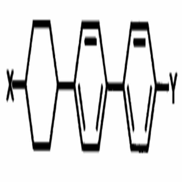
상기 식에서,Where
X와 Y는 서로 독립적으로, R1 또는 OR2이며, R1과 R2는 서로 독립적으로 탄소수가 1 내지 5개인 알킬 그룹 또는 알케닐 그룹이다.X and Y are independently of each other, R1 or OR2, and R1 and R2 are independently of each other an alkyl group or alkenyl group having 1 to 5 carbon atoms.
액정조성물은 상기 X와 Y 중 적어도 어느 하나가 알케닐 그룹을 포함하는 화합물은 5%이하인 것이 바람직하다.In the liquid crystal composition, at least one of the compounds containing at least one of an alkenyl group is preferably 5% or less.
상기 액정조성물의 유전율 이방성은 -2.7내지 -5.8인 것이 바람직하다.The dielectric anisotropy of the liquid crystal composition is preferably -2.7 to -5.8.
상기 액정조성물의 굴절율 이방성은 0.075 내지 0.109인 것이 바람직하다.It is preferable that the refractive index anisotropy of the liquid crystal composition is 0.075 to 0.109.
상기 액정조성물의 회전점도는 87mPa·s 내지 165mPa·s인 것이 바람직하다.It is preferable that the rotational viscosity of the said liquid-crystal composition is 87 mPa * s-165 mPa * s.
상기 본 발명의 목적은 박막트랜지스터와, 상기 박막트랜지스터에 전기적으로 연결된 화소전극을 포함하는 제1기판과; 상기 제1기판과 마주하며 공통전극을 포함하는 제2기판과; 상기 제1기판과 상기 제2기판 사이에 위치하며 상기 액정조성물을 포함하는 액정표시장치에 의하여 달성된다.An object of the present invention is a first substrate comprising a thin film transistor and a pixel electrode electrically connected to the thin film transistor; A second substrate facing the first substrate and including a common electrode; It is achieved by a liquid crystal display device positioned between the first substrate and the second substrate and including the liquid crystal composition.
상기 화소전극에는 화소전극 절개패턴이 형성되어 있으며, 상기 공통전극에는 공통전극 절개패턴이 형성되어 있는 것이 바람직하다.The pixel electrode cutting pattern is formed on the pixel electrode, and the common electrode cutting pattern is formed on the common electrode.
이하 첨부된 도면을 참조로 하여 본 발명을 더욱 상세히 설명하겠다. 이하에서 어떤 막(층)이 다른 막(층)의 '상부에 형성되어(위치하고) 있다는 것은, 두 막(층)이 접해 있는 경우 뿐 아니라 두 막(층) 사이에 다른 막(층)이 존재하는 경우도 포함한다.Hereinafter, the present invention will be described in more detail with reference to the accompanying drawings. In the following description, a film is formed (located) on top of another film, not only when two films are in contact with each other but also between the two films. It also includes the case.
도 1 내지 도 2를 참조하여 본 발명에 따른 액정표시장치를 설명한다.A liquid crystal display according to the present invention will be described with reference to FIGS. 1 and 2.
액정표시장치(1)는 박막트랜지스터(T)가 형성되어 있는 제1기판(100), 제1기판(100)과 대향하는 제2기판(200), 양 기판(100, 200) 사이에 위치하는 액정층(300)을 포함한다. The liquid
먼저 제1 기판(100)에 대하여 설명한다.First, the
제1절연기판(111) 상에 게이트 배선(121, 122)이 형성되어 있다. 게이트 배선(121, 122)은 금속 단일층 또는 다중층일 수 있다. 게이트 배선(121, 122)은 표시영역 내에 위치하며 가로 방향으로 뻗어 있는 게이트선(121), 게이트선(121)에서 연결되어 있는 게이트 전극(122)을 포함한다.
제1절연기판(111)위에는 실리콘 질화물(SiNx) 등으로 이루어진 게이트 절연막(131)이 게이트 배선(121, 122)을 덮고 있다.On the first
게이트 전극(122)의 게이트 절연막(131) 상부에는 비정질 실리콘 등의 반도체로 이루어진 반도체층(132)이 형성되어 있으며, 반도체층(132)의 상부에는 실리사이드 또는 n형 불순물이 고농도로 도핑되어 있는 n+ 수소화 비정질 실리콘 등의 물질로 만들어진 저항 접촉층(133)이 형성되어 있다. 소스 전극(142)과 드레인 전극(143) 사이의 채널부에서는 저항 접촉층(133)이 제거되어 있다.A
저항 접촉층(133) 및 게이트 절연막(131) 위에는 데이터 배선(141, 142, 143)이 형성되어 있다. 데이터 배선(141, 142, 143) 역시 금속층으로 이루어진 단일층 또는 다중층일 수 있다. 데이터 배선(141, 142, 143)은 세로방향으로 형성되어 게이트선(121)과 교차하여 화소를 형성하는 데이터선(141), 데이터선(141)의 분지이며 저항 접촉층(133)의 상부까지 연장되어 있는 소스 전극(142), 소스전극(142)과 분리되어 있으며 소스전극(142)의 반대쪽 저항 접촉층(133) 상부에 형성되어 있는 드레인 전극(143)을 포함한다.
데이터 패드(145)는 데이터 구동부(도시하지 않음)에 연결되어, 데이터 구동 신호를 인가받는다. 데이터 패드(145)는 데이터 본선(141)에 비해 폭이 크게 마련되어 있다.The data pad 145 is connected to a data driver (not shown) and receives a data driving signal. The data pad 145 is larger in width than the data
데이터 배선(141, 142, 143) 및 이들이 가리지 않는 반도체층(132)의 상부에는 보호막(151)이 형성되어 있다. 보호막(151)에는 드레인 전극(143)을 드러내는 접촉구(152)가 형성되어 있다. The
보호막(151)의 상부에는 화소전극(161)이 형성되어 있다. 화소전극(161)은 통상 ITO(indium tin oxide) 또는 IZO(indium zinc oxide)등의 투명한 도전물질로 이루어진다. 화소전극(161)은 접촉구(152)를 통해 드레인 전극(143)과 연결되어 있다. 화소전극(161)에는 화소전극 절개패턴(162)가 형성되어 있다. The
화소전극(161)의 화소전극 절개패턴(162)은 후술하는 공통전극 절개패턴(252)과 함께 액정층(300)을 다수의 영역으로 분할한다.The pixel electrode cutting pattern 162 of the
이어 제2 기판(200)에 대하여 설명하겠다.Next, the
제2절연기판(211) 위에 블랙매트릭스(221)가 형성되어 있다. 블랙매트릭스(221)는 일반적으로 적색, 녹색 및 청색 필터 사이를 구분하며, 제1기판(100)에 위치하는 박막트랜지스터로의 직접적인 광조사를 차단하는 역할을 한다. 블랙매트릭스(221)는 통상 검은색 안료가 첨가된 감광성 유기물질로 이루어져 있다. 상기 검은색 안료로는 카본블랙이나 티타늄 옥사이드 등을 사용한다.The
컬러필터(231)는 블랙매트릭스(221)를 경계로 하여 적색, 녹색 및 청색 필터가 반복되어 형성된다. 컬러필터(231)는 백라이트 유닛(도시하지 않음)으로부터 조사되어 액정층(300)을 통과한 빛에 색상을 부여하는 역할을 한다. 컬러필터(231)는 통상 감광성 유기물질로 이루어져 있다.The
컬러필터(231)와 컬러필터(231)가 덮고 있지 않은 블랙매트릭스(221)의 상부에는 오버코트층(241)이 형성되어 있다. 오버코트층(241)은 컬러필터(231)를 평탄화하면서, 컬러필터(231)를 보호하는 역할을 한다. 오버코트층(241)은 감광성 아 크릴계 수지일 수 있다.An
오버코트층(241)의 상부에는 공통전극(251)이 형성되어 있다. 공통전극(251)은 ITO(indium tin oxide) 또는 IZO(indium zinc oxide)등의 투명한 도전물질로 이루어진다. 공통전극(251)은 박막트랜지스터 기판의 화소전극(161)과 함께 액정층(300)에 직접 전압을 인가한다. The
공통전극(251)에는 공통전극 절개패턴(252)이 형성되어 있다. 공통전극 절개패턴(252)은 화소전극(161)의 화소전극 절개패턴(162)과 함께 액정층(300)을 다수의 영역으로 나누는 역할을 한다.The common
화소전극 절개패턴(162)과 공통전극 절개패턴(252)은 실시예에 한정되지 않고 다양한 형상으로 형성될 수 있다. 또한 화소전극(161)의 서로 분리된 복수개의 영역으로 나누어지고, 각 영역에 서로 다른 크기의 전기신호가 입력되는 것도 가능하다.The pixel electrode cut pattern 162 and the common
제1기판(100)과 제2기판(200)의 사이에는 액정층(300)이 위치한다. 액정층(300)은 VA(vertically aligned)모드로서, 액정분자는 전압이 가해지지 않은 상태에서는 길이방향이 수직을 이루고 있다. 전압이 가해지면 액정분자는 유전율 이방성이 음이기 때문에 전기장에 대하여 수직방향으로 눕는다. The
절개패턴(162, 252)이 형성되어 있지 않으면, 액정분자는 눕는 방위각이 결정되지 않아서 여러 방향으로 무질서하게 배열하게 되고, 배향 방향이 다른 경계면에서 전경선(disclination line)이 생긴다. 절개 패턴(162, 252)은 액정층(300)에 전압이 걸릴 때 프린지 필드를 만들어 액정 배향의 방위각을 결정해 준다. 또한 액정층(300)은 절개 패턴(162, 252)의 배치에 따라 복수의 도메인으로 나누어진다.If the
도메인 중 어느 하나의 폭(도 2의 d1)은 절개패턴(162, 252)의 간격에 의해 결정된다. 각 도메인의 중앙부분(A)은 프린지 필드가 약하게 작용하거나 혹은 작용하지 않는다. 따라서 각 도메인의 중간부분에 위치하는 액정층(300)은 주변의 액정층(300)의 움직임에 연동하여 움직이게 되므로 응답속도가 느리게 된다. 응답속도를 개선하기 위해서는 절개패턴(162, 252)의 간격을 줄이면 휘도가 감소하는 문제가 있다.The width of one of the domains (d1 in FIG. 2) is determined by the spacing of the
본 발명에 따른 액정층(300)은 응답속도가 개선되어 도메인의 폭을 유지하면서도 응답속도를 증가시킬 수 있다. 또한 액정층(300)의 빠른 응답속도를 이용해 도메인의 폭을 증가시켜 개구율을 증가시킬 수 있음은 물론이다.In the
본 발명의 액정층(300)은 다음에 설명하는 액정조성물을 포함하며, 필요에 따라 공지의 부가제를 함유할 수 있다. 부가제로는 염료, UV안정제 그리고/또는 항산화제를 사용할 수 있다.The
액정조성물은 다음과 같이 이루어져 있다. 이하에서 언급하는 %는 중량%를 의미한다.The liquid crystal composition is composed as follows. % Mentioned below means weight%.
하나 이상의 화학식 1의 화합물 1 : 5 내지 15%,At least one compound of formula 1: 5-15%,
하나 이상의 화학식 2의 화합물 2 : 25 내지 40%, At least one compound of formula 2: 2: 25-40%,
하나 이상의 화학식 3의 화합물 3 : 10 내지 25%, At least one compound of the formula 3: 10-25%,
하나 이상의 화학식 4의 화합물 4 : 20 내지 30%, At least one compound of the formula 4: 20 to 30%,
하나 이상의 화학식 5의 화합물 5 : 15 내지 25%, At least one compound of the formula 5: 15-25%,
하나 이상의 화학식 6의 화합물 6 : 0 내지 10%, At least one compound of the formula 6: 0-10%,
하나 이상의 화학식 7의 화합물 7 : 0 내지 10%, At least one compound of formula 7: 0 to 10%,
하나 이상의 화학식 8의 화합물 8 : 0 내지 10%At least one compound of formula 8: 0-10%
화학식에서 X와 Y는 서로 독립적으로, R1 또는 OR2이며, R1과 R2는 서로 독립적으로 탄소수가 1 내지 5개인 알킬 그룹 또는 알케닐 그룹이다. X and Y in the formula are independently of each other, R1 or OR2, R1 and R2 independently of each other is an alkyl group or alkenyl group having 1 to 5 carbon atoms.
예를 들어, X와 Y는 CH3, C2H5, C3H7, C4H9, C5H11, OCH3, 0C2H5, OC3H7, OC4H9, OC5H11과 같이 탄소이중결합을 포함하지 않는 물질이거나, C2H4, C2H4, C3H6, C4H8, C5H11, 0C2H4, OC3H6, OC4H8, OC5H10과 같이 탄소이중결합을 포함하는 물질일 수 있다. X와 Y는 탄소이중결합을 2개 이상 포함할 수도 있다.For example, X and Y are CH 3 , C 2 H 5 , C 3 H 7 , C 4 H 9 , C 5 H 11 , OCH 3 , 0C 2 H 5 , OC 3 H 7 , OC 4 H 9 , OC Or a substance that does not contain a carbon double bond, such as 5 H 11 , C 2 H 4 , C 2 H 4 , C 3 H 6 , C 4 H 8 , C 5 H 11 , 0C 2 H 4 , OC 3 H 6 , It may be a material containing a carbon double bond, such as OC 4 H 8 , OC 5 H 10 . X and Y may contain two or more carbon double bonds.
액정조성물 중 X 또는 Y가 탄소이중결합을 포함하는 화합물은 5%이하인 것이 바람직한데, 이들 화합물이 5%이상 포함되면 선잔상 등을 야기하여 신뢰성이 저하된다.In the liquid crystal composition, the compound in which X or Y contains a carbon double bond is preferably 5% or less, but when 5% or more of these compounds are included, the afterimage causes an afterimage, and thus the reliability is lowered.
위 화합물 중 디-플로로 벤젠(di-fluoro benzene)을 포함하는 화합물 3, 화합물 4, 화합물 5, 화합물 8은 액정조성물에 음의 유전율을 부여한다.Compound 3, compound 4, compound 5 and compound 8 containing di-fluoro benzene of the above compound imparts a negative dielectric constant to the liquid crystal composition.
액정조성물의 유전율 이방성(Δε)은 -2.7내지 -5.8, 굴절율 이방성(Δn)은 0.075 내지 0.109, 상기 액정조성물의 회전점도(γ1)는 87mPa·s 내지 165mPa·s이 다.The dielectric anisotropy (Δε) of the liquid crystal composition is -2.7 to -5.8, the refractive index anisotropy (Δn) is 0.075 to 0.109, and the rotational viscosity (γ1) of the liquid crystal composition is 87 mPa · s to 165 mPa · s.
실험을 통해 다양한 조성의 액정조성물에 대하여 물성과 응답속도를 측정하였다.Through experiments, physical properties and response speeds of liquid crystal compositions of various compositions were measured.
실험에 사용된 액정조성물은 실시예 1 내지 실시예 4와 상용으로 사용되고 있는 비교예 등 5가지이다. 실시예 1 내지 실시예 4의 조성은 다음과 표 1과 같다.The liquid crystal composition used for the experiment is five kinds, such as the comparative example used in commercial use with Examples 1 to 4. The composition of Examples 1 to 4 is shown in Table 1 below.
<표 1>TABLE 1
단위 : %unit : %
비교예는 다음과 같은 화합물을 포함한다.Comparative Examples include the following compounds.

실시예 및 비교예에 따른 액정조성물의 물성은 다음 표 2와 같다.Physical properties of the liquid crystal composition according to the Examples and Comparative Examples are shown in Table 2 below.
<표 2>TABLE 2
응답시간은 셀갭(도 2의 d)을 약 3.5㎛ 내지 약 4㎛ 사이에서 변경하면서 측정하였으며, Δnd(여기서 Δn은 굴절율 이방성, d는 셀갭)는 동일하게 유지하였다.The response time was measured while varying the cell gap (d in FIG. 2) between about 3.5 μm and about 4 μm, and Δnd (where Δn is refractive index anisotropy and d is the cell gap) was kept the same.
액정의 응답속도는 라이징 타임만을 측정하였다.The response speed of the liquid crystal measured only the rising time.
액정의 응답속도(Tr)는 라이징 타임(rising time. Ton)과 폴링 타임(falling time, Toff)을 합하여 정한다. 노말리 블랙 모드(normally black mode)에서 라이징 타임은 10% 투과율에서 90% 투과율이 되는 시간으로 정의되고, 폴링 타임은 반대로 90% 투과율에서 10% 투과율이 되는 시간으로 정의된다. 폴링 타임은 액정에 관계없이 약 6ms인 반면 라이징 타임은 액정에 크게 영향받는다. 액정의 응답속도가 느리면 동영상 번짐(motion blur) 현상이 발생하여 디스플레이 품질이 저하된다. The response speed Tr of the liquid crystal is determined by adding a rising time (Ton) and a falling time (Toff). In normally black mode, the rising time is defined as the time from 10% transmittance to 90% transmittance, while the polling time is defined as the time from 90% transmittance to 10% transmittance. The polling time is about 6 ms regardless of the liquid crystal, while the rising time is greatly affected by the liquid crystal. If the response speed of the liquid crystal is slow, motion blur occurs and the display quality is degraded.
실험결과를 나타낸 도 3을 보면 실시예 1 내지 실시예4는 셀갭에 상관없이 비교예보다 짧은 라이징 타임을 나타내었다.Referring to FIG. 3 showing the experimental results, Examples 1 to 4 showed shorter rising times than the comparative examples regardless of the cell gap.
따라서 실시예의 액정조성물을 사용하면 응답속도 그리고/또는 개구율을 향상시킬 수 있다.Therefore, using the liquid crystal composition of the embodiment can improve the response speed and / or aperture ratio.
비록 본발명의 실시예가 도시되고 설명되었지만, 본발명이 속하는 기술분야의 통상의 지식을 가진 당업자라면 본발명의 원칙이나 정신에서 벗어나지 않으면서 본 실시예를 변형할 수 있음을 알 수 있을 것이다. 본발명의 범위는 첨부된 청구항과 그 균등물에 의해 정해질 것이다.Although embodiments of the present invention have been shown and described, it will be apparent to those skilled in the art that the present embodiments may be modified without departing from the spirit or principles of the present invention. It is intended that the scope of the invention be defined by the claims appended hereto and their equivalents.
이상 설명한 바와 같이, 본 발명에 따르면, 응답속도가 개선된 액정조성물과 이를 포함하는 액정표시장치가 제공된다.As described above, according to the present invention, a liquid crystal composition having an improved response speed and a liquid crystal display device including the same are provided.
Claims (7)


Priority Applications (2)
| Application Number | Priority Date | Filing Date | Title |
|---|---|---|---|
| KR1020060115468A KR20080046039A (en) | 2006-11-21 | 2006-11-21 | Liquid crystal composition and liquid crystlal display device having the same |
| US11/932,387 US7666481B2 (en) | 2006-11-21 | 2007-10-31 | Liquid crystal composition and liquid crystal display device having the same |
Applications Claiming Priority (1)
| Application Number | Priority Date | Filing Date | Title |
|---|---|---|---|
| KR1020060115468A KR20080046039A (en) | 2006-11-21 | 2006-11-21 | Liquid crystal composition and liquid crystlal display device having the same |
Publications (1)
| Publication Number | Publication Date |
|---|---|
| KR20080046039A true KR20080046039A (en) | 2008-05-26 |
Family
ID=39416584
Family Applications (1)
| Application Number | Title | Priority Date | Filing Date |
|---|---|---|---|
| KR1020060115468A KR20080046039A (en) | 2006-11-21 | 2006-11-21 | Liquid crystal composition and liquid crystlal display device having the same |
Country Status (2)
| Country | Link |
|---|---|
| US (1) | US7666481B2 (en) |
| KR (1) | KR20080046039A (en) |
Families Citing this family (8)
| Publication number | Priority date | Publication date | Assignee | Title |
|---|---|---|---|---|
| DE102008064171A1 (en) * | 2008-12-22 | 2010-07-01 | Merck Patent Gmbh | Liquid crystalline medium |
| EP2463355B1 (en) * | 2010-12-07 | 2014-08-13 | Merck Patent GmbH | Liquid crystal medium and liquid crystal display |
| CN103249808B (en) * | 2010-12-07 | 2016-05-25 | 默克专利股份有限公司 | Liquid crystal media and liquid crystal display |
| RU2570031C1 (en) * | 2012-10-12 | 2015-12-10 | Дик Корпорейшн | Liquid crystal composition and liquid crystal display element made using same |
| KR20150109543A (en) * | 2014-03-19 | 2015-10-02 | 삼성디스플레이 주식회사 | Liquid crystal composition and liquid crystal display device comprising the same |
| KR102186565B1 (en) * | 2014-05-09 | 2020-12-04 | 삼성디스플레이 주식회사 | Liquid crystal display device |
| KR20190033679A (en) | 2017-09-21 | 2019-04-01 | 삼성디스플레이 주식회사 | Liquid crystal composition and display device comprising the same |
| KR20210063515A (en) * | 2019-11-22 | 2021-06-02 | 삼성디스플레이 주식회사 | Liquid crystal composition and display device comprising the same |
Family Cites Families (7)
| Publication number | Priority date | Publication date | Assignee | Title |
|---|---|---|---|---|
| US5599480A (en) | 1994-07-28 | 1997-02-04 | Merck Patent Gesellschaft Mit Beschrankter Haftung | Liquid-crystalline medium |
| DE19959033A1 (en) * | 1999-12-08 | 2001-06-13 | Merck Patent Gmbh | Liquid crystalline medium |
| DE10112955B4 (en) * | 2000-04-14 | 2010-09-09 | Merck Patent Gmbh | Liquid-crystalline medium and its use |
| JP4019697B2 (en) * | 2001-11-15 | 2007-12-12 | 株式会社日立製作所 | Liquid crystal display |
| JP3881248B2 (en) * | 2002-01-17 | 2007-02-14 | 株式会社日立製作所 | Liquid crystal display device and image display device |
| ATE483780T1 (en) * | 2002-11-22 | 2010-10-15 | Merck Patent Gmbh | LIQUID CRYSTALLINE MEDIUM |
| KR20060059192A (en) * | 2004-11-26 | 2006-06-01 | 메르크 파텐트 게엠베하 | Liquid crystal medium |
-
2006
- 2006-11-21 KR KR1020060115468A patent/KR20080046039A/en not_active Application Discontinuation
-
2007
- 2007-10-31 US US11/932,387 patent/US7666481B2/en active Active
Also Published As
| Publication number | Publication date |
|---|---|
| US7666481B2 (en) | 2010-02-23 |
| US20080117379A1 (en) | 2008-05-22 |
Similar Documents
| Publication | Publication Date | Title |
|---|---|---|
| US8685502B2 (en) | Liquid crystal display | |
| KR20080046039A (en) | Liquid crystal composition and liquid crystlal display device having the same | |
| KR102068961B1 (en) | liquid crystal material and liquid crystal display device including the same | |
| KR101365111B1 (en) | Liquid crystal composition and liquid crystal display apparatus using the same | |
| JP2008144135A (en) | Liquid crystal composition and liquid crystal display device comprising the same | |
| JP2008202049A (en) | Liquid crystal and liquid crystal display using the same | |
| KR20110021587A (en) | Liquid crystal device and manufacturing method of the same | |
| KR20090068709A (en) | Liquid crystal composition and liquid crystlal display device having the same | |
| KR20090024031A (en) | Display device | |
| KR20120117952A (en) | Liquid crystal composition and liquid crystal display comprising the same | |
| KR101427588B1 (en) | Liquid crystal composition and liquid crystlal display device having the same | |
| KR20150086123A (en) | Liquid crystal display | |
| KR20100047575A (en) | Liquid crystal display | |
| US9891491B2 (en) | Liquid crystal display device | |
| KR20160132230A (en) | Liquid crystal composition and liquid crystal display including the same | |
| KR102312261B1 (en) | Liquid crystal composition and liquid crystal display including the same | |
| JP4378282B2 (en) | High-speed and high-temperature nematic liquid crystal composition and liquid crystal display device containing the same | |
| KR102350511B1 (en) | Liquid crystal composition and liquid crystal display including the same | |
| US11959006B2 (en) | Liquid crystal display device | |
| KR20190047160A (en) | Liquid crystal composition and display device comprising the same | |
| JP2005521902A (en) | Vertical alignment type liquid crystal display device | |
| CN112835234B (en) | Display device | |
| KR20060062908A (en) | Liquid crystal display panel | |
| KR20090070042A (en) | Liquid crystal composition and liquid crystlal display device having the same | |
| KR20190033679A (en) | Liquid crystal composition and display device comprising the same |
Legal Events
| Date | Code | Title | Description |
|---|---|---|---|
| A201 | Request for examination | ||
| N231 | Notification of change of applicant | ||
| E902 | Notification of reason for refusal | ||
| E601 | Decision to refuse application |