JP2009038353A - Liquid crystal display device - Google Patents
Liquid crystal display device Download PDFInfo
- Publication number
- JP2009038353A JP2009038353A JP2008168468A JP2008168468A JP2009038353A JP 2009038353 A JP2009038353 A JP 2009038353A JP 2008168468 A JP2008168468 A JP 2008168468A JP 2008168468 A JP2008168468 A JP 2008168468A JP 2009038353 A JP2009038353 A JP 2009038353A
- Authority
- JP
- Japan
- Prior art keywords
- electrode
- source
- film
- semiconductor film
- liquid crystal
- Prior art date
- Legal status (The legal status is an assumption and is not a legal conclusion. Google has not performed a legal analysis and makes no representation as to the accuracy of the status listed.)
- Withdrawn
Links
- 239000004973 liquid crystal related substance Substances 0.000 title claims abstract description 165
- 239000010408 film Substances 0.000 claims abstract description 590
- 239000004065 semiconductor Substances 0.000 claims abstract description 256
- 239000010409 thin film Substances 0.000 claims abstract description 200
- IJGRMHOSHXDMSA-UHFFFAOYSA-N Atomic nitrogen Chemical compound N#N IJGRMHOSHXDMSA-UHFFFAOYSA-N 0.000 claims description 38
- UFHFLCQGNIYNRP-UHFFFAOYSA-N Hydrogen Chemical compound [H][H] UFHFLCQGNIYNRP-UHFFFAOYSA-N 0.000 claims description 33
- 239000001257 hydrogen Substances 0.000 claims description 31
- 229910052739 hydrogen Inorganic materials 0.000 claims description 31
- 229910052757 nitrogen Inorganic materials 0.000 claims description 19
- 239000011737 fluorine Substances 0.000 claims description 13
- 229910052731 fluorine Inorganic materials 0.000 claims description 13
- 239000000460 chlorine Substances 0.000 claims description 9
- ZCYVEMRRCGMTRW-UHFFFAOYSA-N 7553-56-2 Chemical compound [I] ZCYVEMRRCGMTRW-UHFFFAOYSA-N 0.000 claims description 5
- WKBOTKDWSSQWDR-UHFFFAOYSA-N Bromine atom Chemical compound [Br] WKBOTKDWSSQWDR-UHFFFAOYSA-N 0.000 claims description 5
- ZAMOUSCENKQFHK-UHFFFAOYSA-N Chlorine atom Chemical compound [Cl] ZAMOUSCENKQFHK-UHFFFAOYSA-N 0.000 claims description 5
- GDTBXPJZTBHREO-UHFFFAOYSA-N bromine Substances BrBr GDTBXPJZTBHREO-UHFFFAOYSA-N 0.000 claims description 5
- 229910052794 bromium Inorganic materials 0.000 claims description 5
- 229910052801 chlorine Inorganic materials 0.000 claims description 5
- 239000011630 iodine Substances 0.000 claims description 5
- 229910052740 iodine Inorganic materials 0.000 claims description 5
- PXGOKWXKJXAPGV-UHFFFAOYSA-N Fluorine Chemical compound FF PXGOKWXKJXAPGV-UHFFFAOYSA-N 0.000 claims 1
- 230000015572 biosynthetic process Effects 0.000 abstract description 63
- 238000004519 manufacturing process Methods 0.000 abstract description 23
- 230000006870 function Effects 0.000 abstract description 12
- 239000000758 substrate Substances 0.000 description 110
- 239000010410 layer Substances 0.000 description 91
- 239000007789 gas Substances 0.000 description 56
- 238000000034 method Methods 0.000 description 53
- 239000012535 impurity Substances 0.000 description 52
- 238000006243 chemical reaction Methods 0.000 description 42
- 229910021417 amorphous silicon Inorganic materials 0.000 description 34
- BLRPTPMANUNPDV-UHFFFAOYSA-N Silane Chemical compound [SiH4] BLRPTPMANUNPDV-UHFFFAOYSA-N 0.000 description 33
- 229910021424 microcrystalline silicon Inorganic materials 0.000 description 29
- 238000012545 processing Methods 0.000 description 29
- 229910052990 silicon hydride Inorganic materials 0.000 description 28
- XUIMIQQOPSSXEZ-UHFFFAOYSA-N Silicon Chemical compound [Si] XUIMIQQOPSSXEZ-UHFFFAOYSA-N 0.000 description 25
- 239000013078 crystal Substances 0.000 description 25
- 229910052710 silicon Inorganic materials 0.000 description 25
- 239000010703 silicon Substances 0.000 description 25
- 238000005268 plasma chemical vapour deposition Methods 0.000 description 23
- XKRFYHLGVUSROY-UHFFFAOYSA-N Argon Chemical compound [Ar] XKRFYHLGVUSROY-UHFFFAOYSA-N 0.000 description 22
- 229910052581 Si3N4 Inorganic materials 0.000 description 22
- 239000003990 capacitor Substances 0.000 description 22
- HQVNEWCFYHHQES-UHFFFAOYSA-N silicon nitride Chemical compound N12[Si]34N5[Si]62N3[Si]51N64 HQVNEWCFYHHQES-UHFFFAOYSA-N 0.000 description 22
- 230000005684 electric field Effects 0.000 description 19
- 230000008569 process Effects 0.000 description 19
- 230000001681 protective effect Effects 0.000 description 17
- 229910052734 helium Inorganic materials 0.000 description 14
- 239000001307 helium Substances 0.000 description 14
- SWQJXJOGLNCZEY-UHFFFAOYSA-N helium atom Chemical compound [He] SWQJXJOGLNCZEY-UHFFFAOYSA-N 0.000 description 14
- 229910052786 argon Inorganic materials 0.000 description 11
- QVGXLLKOCUKJST-UHFFFAOYSA-N atomic oxygen Chemical compound [O] QVGXLLKOCUKJST-UHFFFAOYSA-N 0.000 description 11
- 238000005530 etching Methods 0.000 description 11
- 229910052743 krypton Inorganic materials 0.000 description 11
- DNNSSWSSYDEUBZ-UHFFFAOYSA-N krypton atom Chemical compound [Kr] DNNSSWSSYDEUBZ-UHFFFAOYSA-N 0.000 description 11
- 239000001301 oxygen Substances 0.000 description 11
- VYPSYNLAJGMNEJ-UHFFFAOYSA-N Silicium dioxide Chemical compound O=[Si]=O VYPSYNLAJGMNEJ-UHFFFAOYSA-N 0.000 description 10
- 229910052760 oxygen Inorganic materials 0.000 description 10
- 239000000463 material Substances 0.000 description 9
- 229910052814 silicon oxide Inorganic materials 0.000 description 9
- 125000006850 spacer group Chemical group 0.000 description 9
- 238000002834 transmittance Methods 0.000 description 9
- QGZKDVFQNNGYKY-UHFFFAOYSA-N Ammonia Chemical compound N QGZKDVFQNNGYKY-UHFFFAOYSA-N 0.000 description 8
- YCKRFDGAMUMZLT-UHFFFAOYSA-N Fluorine atom Chemical compound [F] YCKRFDGAMUMZLT-UHFFFAOYSA-N 0.000 description 8
- ZOKXTWBITQBERF-UHFFFAOYSA-N Molybdenum Chemical compound [Mo] ZOKXTWBITQBERF-UHFFFAOYSA-N 0.000 description 8
- GQPLMRYTRLFLPF-UHFFFAOYSA-N Nitrous Oxide Chemical compound [O-][N+]#N GQPLMRYTRLFLPF-UHFFFAOYSA-N 0.000 description 8
- 238000000151 deposition Methods 0.000 description 8
- 230000008021 deposition Effects 0.000 description 8
- 229910052750 molybdenum Inorganic materials 0.000 description 8
- 239000011733 molybdenum Substances 0.000 description 8
- 238000003860 storage Methods 0.000 description 8
- 229910052782 aluminium Inorganic materials 0.000 description 7
- XAGFODPZIPBFFR-UHFFFAOYSA-N aluminium Chemical compound [Al] XAGFODPZIPBFFR-UHFFFAOYSA-N 0.000 description 7
- 239000012298 atmosphere Substances 0.000 description 7
- 229910052736 halogen Inorganic materials 0.000 description 7
- 150000002367 halogens Chemical class 0.000 description 7
- 229910052754 neon Inorganic materials 0.000 description 7
- GKAOGPIIYCISHV-UHFFFAOYSA-N neon atom Chemical compound [Ne] GKAOGPIIYCISHV-UHFFFAOYSA-N 0.000 description 7
- ZOXJGFHDIHLPTG-UHFFFAOYSA-N Boron Chemical compound [B] ZOXJGFHDIHLPTG-UHFFFAOYSA-N 0.000 description 6
- 229910052796 boron Inorganic materials 0.000 description 6
- 238000004040 coloring Methods 0.000 description 6
- 230000005669 field effect Effects 0.000 description 6
- 230000003647 oxidation Effects 0.000 description 6
- 238000007254 oxidation reaction Methods 0.000 description 6
- 238000004088 simulation Methods 0.000 description 6
- 238000004544 sputter deposition Methods 0.000 description 6
- RTAQQCXQSZGOHL-UHFFFAOYSA-N Titanium Chemical compound [Ti] RTAQQCXQSZGOHL-UHFFFAOYSA-N 0.000 description 5
- 239000000969 carrier Substances 0.000 description 5
- 230000006866 deterioration Effects 0.000 description 5
- 238000010586 diagram Methods 0.000 description 5
- 238000009826 distribution Methods 0.000 description 5
- 239000011521 glass Substances 0.000 description 5
- 150000002431 hydrogen Chemical class 0.000 description 5
- 230000033001 locomotion Effects 0.000 description 5
- 239000000203 mixture Substances 0.000 description 5
- 229910000077 silane Inorganic materials 0.000 description 5
- 229910052719 titanium Inorganic materials 0.000 description 5
- 239000010936 titanium Substances 0.000 description 5
- OAICVXFJPJFONN-UHFFFAOYSA-N Phosphorus Chemical compound [P] OAICVXFJPJFONN-UHFFFAOYSA-N 0.000 description 4
- 238000001069 Raman spectroscopy Methods 0.000 description 4
- 229910021529 ammonia Inorganic materials 0.000 description 4
- 125000004429 atom Chemical group 0.000 description 4
- 229920001940 conductive polymer Polymers 0.000 description 4
- 238000005520 cutting process Methods 0.000 description 4
- 238000001312 dry etching Methods 0.000 description 4
- 229910052751 metal Inorganic materials 0.000 description 4
- 239000002184 metal Substances 0.000 description 4
- 229960001730 nitrous oxide Drugs 0.000 description 4
- 235000013842 nitrous oxide Nutrition 0.000 description 4
- 239000011574 phosphorus Substances 0.000 description 4
- 229910052698 phosphorus Inorganic materials 0.000 description 4
- 238000009832 plasma treatment Methods 0.000 description 4
- 239000002994 raw material Substances 0.000 description 4
- 239000000565 sealant Substances 0.000 description 4
- 238000009751 slip forming Methods 0.000 description 4
- 230000005236 sound signal Effects 0.000 description 4
- 229910052724 xenon Inorganic materials 0.000 description 4
- FHNFHKCVQCLJFQ-UHFFFAOYSA-N xenon atom Chemical compound [Xe] FHNFHKCVQCLJFQ-UHFFFAOYSA-N 0.000 description 4
- 229910000838 Al alloy Inorganic materials 0.000 description 3
- VYZAMTAEIAYCRO-UHFFFAOYSA-N Chromium Chemical compound [Cr] VYZAMTAEIAYCRO-UHFFFAOYSA-N 0.000 description 3
- 239000002585 base Substances 0.000 description 3
- 229910052804 chromium Inorganic materials 0.000 description 3
- 239000011651 chromium Substances 0.000 description 3
- 238000004140 cleaning Methods 0.000 description 3
- 238000007865 diluting Methods 0.000 description 3
- 238000001678 elastic recoil detection analysis Methods 0.000 description 3
- AMGQUBHHOARCQH-UHFFFAOYSA-N indium;oxotin Chemical compound [In].[Sn]=O AMGQUBHHOARCQH-UHFFFAOYSA-N 0.000 description 3
- 238000003780 insertion Methods 0.000 description 3
- 230000037431 insertion Effects 0.000 description 3
- 229910021421 monocrystalline silicon Inorganic materials 0.000 description 3
- 150000004767 nitrides Chemical class 0.000 description 3
- 229920003023 plastic Polymers 0.000 description 3
- 239000004033 plastic Substances 0.000 description 3
- 229920006267 polyester film Polymers 0.000 description 3
- 229920002620 polyvinyl fluoride Polymers 0.000 description 3
- 238000005001 rutherford backscattering spectroscopy Methods 0.000 description 3
- 239000002356 single layer Substances 0.000 description 3
- 229910052715 tantalum Inorganic materials 0.000 description 3
- GUVRBAGPIYLISA-UHFFFAOYSA-N tantalum atom Chemical compound [Ta] GUVRBAGPIYLISA-UHFFFAOYSA-N 0.000 description 3
- WFKWXMTUELFFGS-UHFFFAOYSA-N tungsten Chemical compound [W] WFKWXMTUELFFGS-UHFFFAOYSA-N 0.000 description 3
- 229910052721 tungsten Inorganic materials 0.000 description 3
- 239000010937 tungsten Substances 0.000 description 3
- 238000001039 wet etching Methods 0.000 description 3
- OKTJSMMVPCPJKN-UHFFFAOYSA-N Carbon Chemical compound [C] OKTJSMMVPCPJKN-UHFFFAOYSA-N 0.000 description 2
- MYMOFIZGZYHOMD-UHFFFAOYSA-N Dioxygen Chemical compound O=O MYMOFIZGZYHOMD-UHFFFAOYSA-N 0.000 description 2
- 238000001237 Raman spectrum Methods 0.000 description 2
- 229910003902 SiCl 4 Inorganic materials 0.000 description 2
- GWEVSGVZZGPLCZ-UHFFFAOYSA-N Titan oxide Chemical compound O=[Ti]=O GWEVSGVZZGPLCZ-UHFFFAOYSA-N 0.000 description 2
- WGLPBDUCMAPZCE-UHFFFAOYSA-N Trioxochromium Chemical compound O=[Cr](=O)=O WGLPBDUCMAPZCE-UHFFFAOYSA-N 0.000 description 2
- 206010047571 Visual impairment Diseases 0.000 description 2
- 239000000956 alloy Substances 0.000 description 2
- 230000003321 amplification Effects 0.000 description 2
- 238000004380 ashing Methods 0.000 description 2
- 229910052799 carbon Inorganic materials 0.000 description 2
- 230000015556 catabolic process Effects 0.000 description 2
- 239000000919 ceramic Substances 0.000 description 2
- SLLGVCUQYRMELA-UHFFFAOYSA-N chlorosilicon Chemical compound Cl[Si] SLLGVCUQYRMELA-UHFFFAOYSA-N 0.000 description 2
- 229910000423 chromium oxide Inorganic materials 0.000 description 2
- 238000004891 communication Methods 0.000 description 2
- 239000000356 contaminant Substances 0.000 description 2
- 238000002425 crystallisation Methods 0.000 description 2
- 230000008025 crystallization Effects 0.000 description 2
- 230000006378 damage Effects 0.000 description 2
- 238000013461 design Methods 0.000 description 2
- 238000011161 development Methods 0.000 description 2
- 238000009792 diffusion process Methods 0.000 description 2
- 238000010790 dilution Methods 0.000 description 2
- 239000012895 dilution Substances 0.000 description 2
- 229910001882 dioxygen Inorganic materials 0.000 description 2
- 208000037265 diseases, disorders, signs and symptoms Diseases 0.000 description 2
- 230000002349 favourable effect Effects 0.000 description 2
- 239000011152 fibreglass Substances 0.000 description 2
- 229910003437 indium oxide Inorganic materials 0.000 description 2
- PJXISJQVUVHSOJ-UHFFFAOYSA-N indium(iii) oxide Chemical compound [O-2].[O-2].[O-2].[In+3].[In+3] PJXISJQVUVHSOJ-UHFFFAOYSA-N 0.000 description 2
- 230000001678 irradiating effect Effects 0.000 description 2
- 239000011159 matrix material Substances 0.000 description 2
- 238000005259 measurement Methods 0.000 description 2
- 239000007769 metal material Substances 0.000 description 2
- 239000013081 microcrystal Substances 0.000 description 2
- QGLKJKCYBOYXKC-UHFFFAOYSA-N nonaoxidotritungsten Chemical compound O=[W]1(=O)O[W](=O)(=O)O[W](=O)(=O)O1 QGLKJKCYBOYXKC-UHFFFAOYSA-N 0.000 description 2
- 238000003199 nucleic acid amplification method Methods 0.000 description 2
- 239000002245 particle Substances 0.000 description 2
- 239000000126 substance Substances 0.000 description 2
- OGIDPMRJRNCKJF-UHFFFAOYSA-N titanium oxide Inorganic materials [Ti]=O OGIDPMRJRNCKJF-UHFFFAOYSA-N 0.000 description 2
- 229910001930 tungsten oxide Inorganic materials 0.000 description 2
- 238000001771 vacuum deposition Methods 0.000 description 2
- YVTHLONGBIQYBO-UHFFFAOYSA-N zinc indium(3+) oxygen(2-) Chemical compound [O--].[Zn++].[In+3] YVTHLONGBIQYBO-UHFFFAOYSA-N 0.000 description 2
- 239000004925 Acrylic resin Substances 0.000 description 1
- 229920000178 Acrylic resin Polymers 0.000 description 1
- RYGMFSIKBFXOCR-UHFFFAOYSA-N Copper Chemical compound [Cu] RYGMFSIKBFXOCR-UHFFFAOYSA-N 0.000 description 1
- 229910019974 CrSi Inorganic materials 0.000 description 1
- 244000126211 Hericium coralloides Species 0.000 description 1
- 229910016006 MoSi Inorganic materials 0.000 description 1
- 229910052779 Neodymium Inorganic materials 0.000 description 1
- 238000006124 Pilkington process Methods 0.000 description 1
- 229910052774 Proactinium Inorganic materials 0.000 description 1
- 239000003513 alkali Substances 0.000 description 1
- 229910045601 alloy Inorganic materials 0.000 description 1
- 239000005407 aluminoborosilicate glass Substances 0.000 description 1
- 239000005354 aluminosilicate glass Substances 0.000 description 1
- 229910052788 barium Inorganic materials 0.000 description 1
- DSAJWYNOEDNPEQ-UHFFFAOYSA-N barium atom Chemical compound [Ba] DSAJWYNOEDNPEQ-UHFFFAOYSA-N 0.000 description 1
- 230000004888 barrier function Effects 0.000 description 1
- 239000011324 bead Substances 0.000 description 1
- 230000008901 benefit Effects 0.000 description 1
- 239000005388 borosilicate glass Substances 0.000 description 1
- 230000001413 cellular effect Effects 0.000 description 1
- 239000007795 chemical reaction product Substances 0.000 description 1
- 238000005229 chemical vapour deposition Methods 0.000 description 1
- 239000004020 conductor Substances 0.000 description 1
- 229920001577 copolymer Polymers 0.000 description 1
- 229910052802 copper Inorganic materials 0.000 description 1
- 239000010949 copper Substances 0.000 description 1
- 230000007423 decrease Effects 0.000 description 1
- 238000010494 dissociation reaction Methods 0.000 description 1
- 230000005593 dissociations Effects 0.000 description 1
- 230000005611 electricity Effects 0.000 description 1
- 239000011888 foil Substances 0.000 description 1
- 238000010438 heat treatment Methods 0.000 description 1
- 239000003779 heat-resistant material Substances 0.000 description 1
- 238000010849 ion bombardment Methods 0.000 description 1
- 238000005499 laser crystallization Methods 0.000 description 1
- 239000007788 liquid Substances 0.000 description 1
- 238000012423 maintenance Methods 0.000 description 1
- 238000002156 mixing Methods 0.000 description 1
- QEFYFXOXNSNQGX-UHFFFAOYSA-N neodymium atom Chemical compound [Nd] QEFYFXOXNSNQGX-UHFFFAOYSA-N 0.000 description 1
- GVGCUCJTUSOZKP-UHFFFAOYSA-N nitrogen trifluoride Chemical compound FN(F)F GVGCUCJTUSOZKP-UHFFFAOYSA-N 0.000 description 1
- 229910052756 noble gas Inorganic materials 0.000 description 1
- 150000002835 noble gases Chemical class 0.000 description 1
- 230000003287 optical effect Effects 0.000 description 1
- 238000007500 overflow downdraw method Methods 0.000 description 1
- 230000001590 oxidative effect Effects 0.000 description 1
- 229910000034 oxygen hydride Inorganic materials 0.000 description 1
- 230000003071 parasitic effect Effects 0.000 description 1
- 230000000737 periodic effect Effects 0.000 description 1
- 238000000206 photolithography Methods 0.000 description 1
- 229920002120 photoresistant polymer Polymers 0.000 description 1
- 229920000767 polyaniline Polymers 0.000 description 1
- 229920000128 polypyrrole Polymers 0.000 description 1
- 229920000123 polythiophene Polymers 0.000 description 1
- 230000002265 prevention Effects 0.000 description 1
- 239000010453 quartz Substances 0.000 description 1
- 230000009467 reduction Effects 0.000 description 1
- 230000004043 responsiveness Effects 0.000 description 1
- 230000002441 reversible effect Effects 0.000 description 1
- 230000000630 rising effect Effects 0.000 description 1
- 229910052706 scandium Inorganic materials 0.000 description 1
- SIXSYDAISGFNSX-UHFFFAOYSA-N scandium atom Chemical compound [Sc] SIXSYDAISGFNSX-UHFFFAOYSA-N 0.000 description 1
- 238000001228 spectrum Methods 0.000 description 1
- 239000010935 stainless steel Substances 0.000 description 1
- 229910001220 stainless steel Inorganic materials 0.000 description 1
- 230000003068 static effect Effects 0.000 description 1
- 238000006557 surface reaction Methods 0.000 description 1
- TXEYQDLBPFQVAA-UHFFFAOYSA-N tetrafluoromethane Chemical compound FC(F)(F)F TXEYQDLBPFQVAA-UHFFFAOYSA-N 0.000 description 1
- 238000012546 transfer Methods 0.000 description 1
- XLYOFNOQVPJJNP-UHFFFAOYSA-N water Chemical compound O XLYOFNOQVPJJNP-UHFFFAOYSA-N 0.000 description 1
Images


Classifications
-
- G—PHYSICS
- G02—OPTICS
- G02F—OPTICAL DEVICES OR ARRANGEMENTS FOR THE CONTROL OF LIGHT BY MODIFICATION OF THE OPTICAL PROPERTIES OF THE MEDIA OF THE ELEMENTS INVOLVED THEREIN; NON-LINEAR OPTICS; FREQUENCY-CHANGING OF LIGHT; OPTICAL LOGIC ELEMENTS; OPTICAL ANALOGUE/DIGITAL CONVERTERS
- G02F1/00—Devices or arrangements for the control of the intensity, colour, phase, polarisation or direction of light arriving from an independent light source, e.g. switching, gating or modulating; Non-linear optics
- G02F1/01—Devices or arrangements for the control of the intensity, colour, phase, polarisation or direction of light arriving from an independent light source, e.g. switching, gating or modulating; Non-linear optics for the control of the intensity, phase, polarisation or colour
- G02F1/13—Devices or arrangements for the control of the intensity, colour, phase, polarisation or direction of light arriving from an independent light source, e.g. switching, gating or modulating; Non-linear optics for the control of the intensity, phase, polarisation or colour based on liquid crystals, e.g. single liquid crystal display cells
- G02F1/133—Constructional arrangements; Operation of liquid crystal cells; Circuit arrangements
- G02F1/136—Liquid crystal cells structurally associated with a semi-conducting layer or substrate, e.g. cells forming part of an integrated circuit
- G02F1/1362—Active matrix addressed cells
- G02F1/136286—Wiring, e.g. gate line, drain line
-
- G—PHYSICS
- G02—OPTICS
- G02F—OPTICAL DEVICES OR ARRANGEMENTS FOR THE CONTROL OF LIGHT BY MODIFICATION OF THE OPTICAL PROPERTIES OF THE MEDIA OF THE ELEMENTS INVOLVED THEREIN; NON-LINEAR OPTICS; FREQUENCY-CHANGING OF LIGHT; OPTICAL LOGIC ELEMENTS; OPTICAL ANALOGUE/DIGITAL CONVERTERS
- G02F1/00—Devices or arrangements for the control of the intensity, colour, phase, polarisation or direction of light arriving from an independent light source, e.g. switching, gating or modulating; Non-linear optics
- G02F1/01—Devices or arrangements for the control of the intensity, colour, phase, polarisation or direction of light arriving from an independent light source, e.g. switching, gating or modulating; Non-linear optics for the control of the intensity, phase, polarisation or colour
- G02F1/13—Devices or arrangements for the control of the intensity, colour, phase, polarisation or direction of light arriving from an independent light source, e.g. switching, gating or modulating; Non-linear optics for the control of the intensity, phase, polarisation or colour based on liquid crystals, e.g. single liquid crystal display cells
- G02F1/133—Constructional arrangements; Operation of liquid crystal cells; Circuit arrangements
- G02F1/136—Liquid crystal cells structurally associated with a semi-conducting layer or substrate, e.g. cells forming part of an integrated circuit
- G02F1/1362—Active matrix addressed cells
- G02F1/1368—Active matrix addressed cells in which the switching element is a three-electrode device
-
- G—PHYSICS
- G02—OPTICS
- G02F—OPTICAL DEVICES OR ARRANGEMENTS FOR THE CONTROL OF LIGHT BY MODIFICATION OF THE OPTICAL PROPERTIES OF THE MEDIA OF THE ELEMENTS INVOLVED THEREIN; NON-LINEAR OPTICS; FREQUENCY-CHANGING OF LIGHT; OPTICAL LOGIC ELEMENTS; OPTICAL ANALOGUE/DIGITAL CONVERTERS
- G02F1/00—Devices or arrangements for the control of the intensity, colour, phase, polarisation or direction of light arriving from an independent light source, e.g. switching, gating or modulating; Non-linear optics
- G02F1/01—Devices or arrangements for the control of the intensity, colour, phase, polarisation or direction of light arriving from an independent light source, e.g. switching, gating or modulating; Non-linear optics for the control of the intensity, phase, polarisation or colour
- G02F1/13—Devices or arrangements for the control of the intensity, colour, phase, polarisation or direction of light arriving from an independent light source, e.g. switching, gating or modulating; Non-linear optics for the control of the intensity, phase, polarisation or colour based on liquid crystals, e.g. single liquid crystal display cells
- G02F1/133—Constructional arrangements; Operation of liquid crystal cells; Circuit arrangements
- G02F1/1333—Constructional arrangements; Manufacturing methods
- G02F1/133345—Insulating layers
-
- G—PHYSICS
- G02—OPTICS
- G02F—OPTICAL DEVICES OR ARRANGEMENTS FOR THE CONTROL OF LIGHT BY MODIFICATION OF THE OPTICAL PROPERTIES OF THE MEDIA OF THE ELEMENTS INVOLVED THEREIN; NON-LINEAR OPTICS; FREQUENCY-CHANGING OF LIGHT; OPTICAL LOGIC ELEMENTS; OPTICAL ANALOGUE/DIGITAL CONVERTERS
- G02F1/00—Devices or arrangements for the control of the intensity, colour, phase, polarisation or direction of light arriving from an independent light source, e.g. switching, gating or modulating; Non-linear optics
- G02F1/01—Devices or arrangements for the control of the intensity, colour, phase, polarisation or direction of light arriving from an independent light source, e.g. switching, gating or modulating; Non-linear optics for the control of the intensity, phase, polarisation or colour
- G02F1/13—Devices or arrangements for the control of the intensity, colour, phase, polarisation or direction of light arriving from an independent light source, e.g. switching, gating or modulating; Non-linear optics for the control of the intensity, phase, polarisation or colour based on liquid crystals, e.g. single liquid crystal display cells
- G02F1/133—Constructional arrangements; Operation of liquid crystal cells; Circuit arrangements
- G02F1/1333—Constructional arrangements; Manufacturing methods
- G02F1/1339—Gaskets; Spacers; Sealing of cells
-
- G—PHYSICS
- G02—OPTICS
- G02F—OPTICAL DEVICES OR ARRANGEMENTS FOR THE CONTROL OF LIGHT BY MODIFICATION OF THE OPTICAL PROPERTIES OF THE MEDIA OF THE ELEMENTS INVOLVED THEREIN; NON-LINEAR OPTICS; FREQUENCY-CHANGING OF LIGHT; OPTICAL LOGIC ELEMENTS; OPTICAL ANALOGUE/DIGITAL CONVERTERS
- G02F1/00—Devices or arrangements for the control of the intensity, colour, phase, polarisation or direction of light arriving from an independent light source, e.g. switching, gating or modulating; Non-linear optics
- G02F1/01—Devices or arrangements for the control of the intensity, colour, phase, polarisation or direction of light arriving from an independent light source, e.g. switching, gating or modulating; Non-linear optics for the control of the intensity, phase, polarisation or colour
- G02F1/13—Devices or arrangements for the control of the intensity, colour, phase, polarisation or direction of light arriving from an independent light source, e.g. switching, gating or modulating; Non-linear optics for the control of the intensity, phase, polarisation or colour based on liquid crystals, e.g. single liquid crystal display cells
- G02F1/133—Constructional arrangements; Operation of liquid crystal cells; Circuit arrangements
- G02F1/1333—Constructional arrangements; Manufacturing methods
- G02F1/1343—Electrodes
- G02F1/134309—Electrodes characterised by their geometrical arrangement
-
- G—PHYSICS
- G02—OPTICS
- G02F—OPTICAL DEVICES OR ARRANGEMENTS FOR THE CONTROL OF LIGHT BY MODIFICATION OF THE OPTICAL PROPERTIES OF THE MEDIA OF THE ELEMENTS INVOLVED THEREIN; NON-LINEAR OPTICS; FREQUENCY-CHANGING OF LIGHT; OPTICAL LOGIC ELEMENTS; OPTICAL ANALOGUE/DIGITAL CONVERTERS
- G02F1/00—Devices or arrangements for the control of the intensity, colour, phase, polarisation or direction of light arriving from an independent light source, e.g. switching, gating or modulating; Non-linear optics
- G02F1/01—Devices or arrangements for the control of the intensity, colour, phase, polarisation or direction of light arriving from an independent light source, e.g. switching, gating or modulating; Non-linear optics for the control of the intensity, phase, polarisation or colour
- G02F1/13—Devices or arrangements for the control of the intensity, colour, phase, polarisation or direction of light arriving from an independent light source, e.g. switching, gating or modulating; Non-linear optics for the control of the intensity, phase, polarisation or colour based on liquid crystals, e.g. single liquid crystal display cells
- G02F1/133—Constructional arrangements; Operation of liquid crystal cells; Circuit arrangements
- G02F1/136—Liquid crystal cells structurally associated with a semi-conducting layer or substrate, e.g. cells forming part of an integrated circuit
- G02F1/1362—Active matrix addressed cells
- G02F1/136209—Light shielding layers, e.g. black matrix, incorporated in the active matrix substrate, e.g. structurally associated with the switching element
-
- H—ELECTRICITY
- H01—ELECTRIC ELEMENTS
- H01L—SEMICONDUCTOR DEVICES NOT COVERED BY CLASS H10
- H01L27/00—Devices consisting of a plurality of semiconductor or other solid-state components formed in or on a common substrate
- H01L27/02—Devices consisting of a plurality of semiconductor or other solid-state components formed in or on a common substrate including semiconductor components specially adapted for rectifying, oscillating, amplifying or switching and having potential barriers; including integrated passive circuit elements having potential barriers
- H01L27/12—Devices consisting of a plurality of semiconductor or other solid-state components formed in or on a common substrate including semiconductor components specially adapted for rectifying, oscillating, amplifying or switching and having potential barriers; including integrated passive circuit elements having potential barriers the substrate being other than a semiconductor body, e.g. an insulating body
- H01L27/1214—Devices consisting of a plurality of semiconductor or other solid-state components formed in or on a common substrate including semiconductor components specially adapted for rectifying, oscillating, amplifying or switching and having potential barriers; including integrated passive circuit elements having potential barriers the substrate being other than a semiconductor body, e.g. an insulating body comprising a plurality of TFTs formed on a non-semiconducting substrate, e.g. driving circuits for AMLCDs
- H01L27/1222—Devices consisting of a plurality of semiconductor or other solid-state components formed in or on a common substrate including semiconductor components specially adapted for rectifying, oscillating, amplifying or switching and having potential barriers; including integrated passive circuit elements having potential barriers the substrate being other than a semiconductor body, e.g. an insulating body comprising a plurality of TFTs formed on a non-semiconducting substrate, e.g. driving circuits for AMLCDs with a particular composition, shape or crystalline structure of the active layer
-
- H—ELECTRICITY
- H01—ELECTRIC ELEMENTS
- H01L—SEMICONDUCTOR DEVICES NOT COVERED BY CLASS H10
- H01L27/00—Devices consisting of a plurality of semiconductor or other solid-state components formed in or on a common substrate
- H01L27/02—Devices consisting of a plurality of semiconductor or other solid-state components formed in or on a common substrate including semiconductor components specially adapted for rectifying, oscillating, amplifying or switching and having potential barriers; including integrated passive circuit elements having potential barriers
- H01L27/12—Devices consisting of a plurality of semiconductor or other solid-state components formed in or on a common substrate including semiconductor components specially adapted for rectifying, oscillating, amplifying or switching and having potential barriers; including integrated passive circuit elements having potential barriers the substrate being other than a semiconductor body, e.g. an insulating body
- H01L27/1214—Devices consisting of a plurality of semiconductor or other solid-state components formed in or on a common substrate including semiconductor components specially adapted for rectifying, oscillating, amplifying or switching and having potential barriers; including integrated passive circuit elements having potential barriers the substrate being other than a semiconductor body, e.g. an insulating body comprising a plurality of TFTs formed on a non-semiconducting substrate, e.g. driving circuits for AMLCDs
- H01L27/1259—Multistep manufacturing methods
- H01L27/1288—Multistep manufacturing methods employing particular masking sequences or specially adapted masks, e.g. half-tone mask
-
- H—ELECTRICITY
- H01—ELECTRIC ELEMENTS
- H01L—SEMICONDUCTOR DEVICES NOT COVERED BY CLASS H10
- H01L29/00—Semiconductor devices specially adapted for rectifying, amplifying, oscillating or switching and having potential barriers; Capacitors or resistors having potential barriers, e.g. a PN-junction depletion layer or carrier concentration layer; Details of semiconductor bodies or of electrodes thereof ; Multistep manufacturing processes therefor
- H01L29/02—Semiconductor bodies ; Multistep manufacturing processes therefor
- H01L29/04—Semiconductor bodies ; Multistep manufacturing processes therefor characterised by their crystalline structure, e.g. polycrystalline, cubic or particular orientation of crystalline planes
-
- H—ELECTRICITY
- H01—ELECTRIC ELEMENTS
- H01L—SEMICONDUCTOR DEVICES NOT COVERED BY CLASS H10
- H01L29/00—Semiconductor devices specially adapted for rectifying, amplifying, oscillating or switching and having potential barriers; Capacitors or resistors having potential barriers, e.g. a PN-junction depletion layer or carrier concentration layer; Details of semiconductor bodies or of electrodes thereof ; Multistep manufacturing processes therefor
- H01L29/40—Electrodes ; Multistep manufacturing processes therefor
- H01L29/41—Electrodes ; Multistep manufacturing processes therefor characterised by their shape, relative sizes or dispositions
- H01L29/417—Electrodes ; Multistep manufacturing processes therefor characterised by their shape, relative sizes or dispositions carrying the current to be rectified, amplified or switched
- H01L29/41725—Source or drain electrodes for field effect devices
- H01L29/41733—Source or drain electrodes for field effect devices for thin film transistors with insulated gate
-
- H—ELECTRICITY
- H01—ELECTRIC ELEMENTS
- H01L—SEMICONDUCTOR DEVICES NOT COVERED BY CLASS H10
- H01L29/00—Semiconductor devices specially adapted for rectifying, amplifying, oscillating or switching and having potential barriers; Capacitors or resistors having potential barriers, e.g. a PN-junction depletion layer or carrier concentration layer; Details of semiconductor bodies or of electrodes thereof ; Multistep manufacturing processes therefor
- H01L29/40—Electrodes ; Multistep manufacturing processes therefor
- H01L29/43—Electrodes ; Multistep manufacturing processes therefor characterised by the materials of which they are formed
- H01L29/45—Ohmic electrodes
- H01L29/456—Ohmic electrodes on silicon
- H01L29/458—Ohmic electrodes on silicon for thin film silicon, e.g. source or drain electrode
-
- H—ELECTRICITY
- H01—ELECTRIC ELEMENTS
- H01L—SEMICONDUCTOR DEVICES NOT COVERED BY CLASS H10
- H01L29/00—Semiconductor devices specially adapted for rectifying, amplifying, oscillating or switching and having potential barriers; Capacitors or resistors having potential barriers, e.g. a PN-junction depletion layer or carrier concentration layer; Details of semiconductor bodies or of electrodes thereof ; Multistep manufacturing processes therefor
- H01L29/66—Types of semiconductor device ; Multistep manufacturing processes therefor
- H01L29/66007—Multistep manufacturing processes
- H01L29/66075—Multistep manufacturing processes of devices having semiconductor bodies comprising group 14 or group 13/15 materials
- H01L29/66227—Multistep manufacturing processes of devices having semiconductor bodies comprising group 14 or group 13/15 materials the devices being controllable only by the electric current supplied or the electric potential applied, to an electrode which does not carry the current to be rectified, amplified or switched, e.g. three-terminal devices
- H01L29/66409—Unipolar field-effect transistors
- H01L29/66477—Unipolar field-effect transistors with an insulated gate, i.e. MISFET
- H01L29/66742—Thin film unipolar transistors
- H01L29/6675—Amorphous silicon or polysilicon transistors
- H01L29/66765—Lateral single gate single channel transistors with inverted structure, i.e. the channel layer is formed after the gate
-
- H—ELECTRICITY
- H01—ELECTRIC ELEMENTS
- H01L—SEMICONDUCTOR DEVICES NOT COVERED BY CLASS H10
- H01L29/00—Semiconductor devices specially adapted for rectifying, amplifying, oscillating or switching and having potential barriers; Capacitors or resistors having potential barriers, e.g. a PN-junction depletion layer or carrier concentration layer; Details of semiconductor bodies or of electrodes thereof ; Multistep manufacturing processes therefor
- H01L29/66—Types of semiconductor device ; Multistep manufacturing processes therefor
- H01L29/68—Types of semiconductor device ; Multistep manufacturing processes therefor controllable by only the electric current supplied, or only the electric potential applied, to an electrode which does not carry the current to be rectified, amplified or switched
- H01L29/76—Unipolar devices, e.g. field effect transistors
- H01L29/772—Field effect transistors
- H01L29/78—Field effect transistors with field effect produced by an insulated gate
- H01L29/786—Thin film transistors, i.e. transistors with a channel being at least partly a thin film
- H01L29/78606—Thin film transistors, i.e. transistors with a channel being at least partly a thin film with supplementary region or layer in the thin film or in the insulated bulk substrate supporting it for controlling or increasing the safety of the device
- H01L29/78618—Thin film transistors, i.e. transistors with a channel being at least partly a thin film with supplementary region or layer in the thin film or in the insulated bulk substrate supporting it for controlling or increasing the safety of the device characterised by the drain or the source properties, e.g. the doping structure, the composition, the sectional shape or the contact structure
-
- H—ELECTRICITY
- H01—ELECTRIC ELEMENTS
- H01L—SEMICONDUCTOR DEVICES NOT COVERED BY CLASS H10
- H01L29/00—Semiconductor devices specially adapted for rectifying, amplifying, oscillating or switching and having potential barriers; Capacitors or resistors having potential barriers, e.g. a PN-junction depletion layer or carrier concentration layer; Details of semiconductor bodies or of electrodes thereof ; Multistep manufacturing processes therefor
- H01L29/66—Types of semiconductor device ; Multistep manufacturing processes therefor
- H01L29/68—Types of semiconductor device ; Multistep manufacturing processes therefor controllable by only the electric current supplied, or only the electric potential applied, to an electrode which does not carry the current to be rectified, amplified or switched
- H01L29/76—Unipolar devices, e.g. field effect transistors
- H01L29/772—Field effect transistors
- H01L29/78—Field effect transistors with field effect produced by an insulated gate
- H01L29/786—Thin film transistors, i.e. transistors with a channel being at least partly a thin film
- H01L29/78651—Silicon transistors
- H01L29/7866—Non-monocrystalline silicon transistors
- H01L29/78672—Polycrystalline or microcrystalline silicon transistor
- H01L29/78678—Polycrystalline or microcrystalline silicon transistor with inverted-type structure, e.g. with bottom gate
-
- H—ELECTRICITY
- H01—ELECTRIC ELEMENTS
- H01L—SEMICONDUCTOR DEVICES NOT COVERED BY CLASS H10
- H01L29/00—Semiconductor devices specially adapted for rectifying, amplifying, oscillating or switching and having potential barriers; Capacitors or resistors having potential barriers, e.g. a PN-junction depletion layer or carrier concentration layer; Details of semiconductor bodies or of electrodes thereof ; Multistep manufacturing processes therefor
- H01L29/66—Types of semiconductor device ; Multistep manufacturing processes therefor
- H01L29/68—Types of semiconductor device ; Multistep manufacturing processes therefor controllable by only the electric current supplied, or only the electric potential applied, to an electrode which does not carry the current to be rectified, amplified or switched
- H01L29/76—Unipolar devices, e.g. field effect transistors
- H01L29/772—Field effect transistors
- H01L29/78—Field effect transistors with field effect produced by an insulated gate
- H01L29/786—Thin film transistors, i.e. transistors with a channel being at least partly a thin film
- H01L29/78696—Thin film transistors, i.e. transistors with a channel being at least partly a thin film characterised by the structure of the channel, e.g. multichannel, transverse or longitudinal shape, length or width, doping structure, or the overlap or alignment between the channel and the gate, the source or the drain, or the contacting structure of the channel
-
- H—ELECTRICITY
- H01—ELECTRIC ELEMENTS
- H01L—SEMICONDUCTOR DEVICES NOT COVERED BY CLASS H10
- H01L29/00—Semiconductor devices specially adapted for rectifying, amplifying, oscillating or switching and having potential barriers; Capacitors or resistors having potential barriers, e.g. a PN-junction depletion layer or carrier concentration layer; Details of semiconductor bodies or of electrodes thereof ; Multistep manufacturing processes therefor
- H01L29/40—Electrodes ; Multistep manufacturing processes therefor
- H01L29/43—Electrodes ; Multistep manufacturing processes therefor characterised by the materials of which they are formed
- H01L29/49—Metal-insulator-semiconductor electrodes, e.g. gates of MOSFET
- H01L29/4908—Metal-insulator-semiconductor electrodes, e.g. gates of MOSFET for thin film semiconductor, e.g. gate of TFT
Landscapes
- Physics & Mathematics (AREA)
- Engineering & Computer Science (AREA)
- Microelectronics & Electronic Packaging (AREA)
- Power Engineering (AREA)
- General Physics & Mathematics (AREA)
- Nonlinear Science (AREA)
- Condensed Matter Physics & Semiconductors (AREA)
- Computer Hardware Design (AREA)
- Chemical & Material Sciences (AREA)
- Crystallography & Structural Chemistry (AREA)
- Ceramic Engineering (AREA)
- Mathematical Physics (AREA)
- Optics & Photonics (AREA)
- Manufacturing & Machinery (AREA)
- Geometry (AREA)
- Thin Film Transistor (AREA)
- Liquid Crystal (AREA)
- Metal-Oxide And Bipolar Metal-Oxide Semiconductor Integrated Circuits (AREA)
- Devices For Indicating Variable Information By Combining Individual Elements (AREA)
Abstract
Description
本発明は、少なくとも画素部に薄膜トランジスタを用いた液晶表示装置に関する。 The present invention relates to a liquid crystal display device using a thin film transistor at least in a pixel portion.
近年、絶縁表面を有する基板上に形成された半導体薄膜(厚さ数十〜数百nm程度)をチャネル形成領域に用いて薄膜トランジスタを構成する技術が注目されている。薄膜トランジスタはICや電気光学装置のような電子デバイスに広く応用され、特に画像表示装置のスイッチング素子として開発が急がれている。 In recent years, a technique for forming a thin film transistor by using a semiconductor thin film (having a thickness of about several tens to several hundreds of nanometers) formed over a substrate having an insulating surface as a channel formation region has attracted attention. Thin film transistors are widely applied to electronic devices such as ICs and electro-optical devices, and development of switching devices for image display devices is urgently required.
画像表示装置のスイッチング素子として、非晶質半導体膜をチャネル形成領域に用いた薄膜トランジスタ、または多結晶半導体膜をチャネル形成領域に用いた薄膜トランジスタ等が用いられている。多結晶半導体膜の形成方法としては、パルス発振のエキシマレーザビームを光学系により線状に加工して、非晶質珪素膜に対し線状ビームを走査させながら照射して結晶化する技術が知られている。 As a switching element of an image display device, a thin film transistor using an amorphous semiconductor film for a channel formation region, a thin film transistor using a polycrystalline semiconductor film for a channel formation region, or the like is used. As a method for forming a polycrystalline semiconductor film, a technique is known in which a pulsed excimer laser beam is processed into a linear shape by an optical system, and is crystallized by irradiating the amorphous silicon film while scanning the linear beam. It has been.
また、画像表示装置のスイッチング素子として、微結晶半導体膜をチャネル形成領域に用いた薄膜トランジスタが用いられている(特許文献1及び2)。
多結晶半導体膜をチャネル形成領域に用いた薄膜トランジスタは、非晶質半導体膜をチャネル形成領域に用いた薄膜トランジスタに比べて電界効果移動度が2桁以上高く、半導体表示装置の画素部とその周辺の駆動回路を同一基板上に一体形成できるという利点を有している。しかしながら、非晶質半導体膜をチャネル形成領域に用いた場合に比べて、半導体膜の結晶化のために工程が複雑化するため、その分歩留まりが低減し、コストが高まるという問題がある。 A thin film transistor using a polycrystalline semiconductor film as a channel formation region has a field effect mobility that is two orders of magnitude higher than a thin film transistor using an amorphous semiconductor film as a channel formation region. This has the advantage that the drive circuit can be integrally formed on the same substrate. However, compared with the case where an amorphous semiconductor film is used for the channel formation region, the process is complicated for crystallization of the semiconductor film, so that there is a problem that the yield is reduced and the cost is increased accordingly.
また、微結晶半導体膜の結晶粒の表面は、酸化されやすいという問題がある。このため、チャネル形成領域の結晶粒が酸化されると、結晶粒の表面に酸化膜が形成されてしまい、当該酸化膜がキャリアの移動の障害となり、薄膜トランジスタの電気特性が低下するという問題がある。 Further, there is a problem that the surface of the crystal grain of the microcrystalline semiconductor film is easily oxidized. For this reason, when the crystal grains in the channel formation region are oxidized, an oxide film is formed on the surface of the crystal grains, and the oxide film becomes an obstacle to the movement of carriers, and there is a problem that the electrical characteristics of the thin film transistor are deteriorated. .
上述した問題に鑑み、本発明は、電気特性が良好であり、信頼性の高い薄膜トランジスタを有する液晶表示装置及びその液晶表示装置を量産高く作製する方法を提案することを課題とする。 In view of the above problems, an object of the present invention is to propose a liquid crystal display device having a thin film transistor with favorable electrical characteristics and high reliability and a method for manufacturing the liquid crystal display device with high mass production.
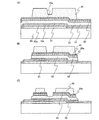
逆スタガ型の薄膜トランジスタを有する液晶表示装置において、逆スタガの薄膜トランジスタは、ゲート電極上にゲート絶縁膜が形成され、ゲート絶縁膜上にチャネル形成領域として機能する微結晶半導体膜(セミアモルファス半導体膜ともいう。)が形成され、微結晶半導体膜上にバッファ層が形成され、バッファ層上に一対のソース領域及びドレイン領域が形成され、ソース領域及びドレイン領域の一部を露出するようにソース領域及びドレイン領域に接する一対のソース電極及びドレイン電極が形成される。このため、ソース領域及びドレイン領域は、ソース電極及びドレイン電極に接する領域と、ソース電極及びドレイン電極に接しない領域とを有する。また、ソース電極及びドレイン電極の外側において、ソース領域及びドレイン領域の一部、並びにバッファ層の一部が露出しており、ソース電極及びドレイン電極は、微結晶半導体膜及びソース領域及びドレイン領域の端部に重ならない。また、ソース電極及びドレイン電極の端部の外側にソース領域及びドレイン領域の端部、並びにバッファ層の端部が形成される。 In a liquid crystal display device including an inverted staggered thin film transistor, a reverse staggered thin film transistor includes a microcrystalline semiconductor film (also referred to as a semi-amorphous semiconductor film) in which a gate insulating film is formed over a gate electrode and functions as a channel formation region over the gate insulating film. A buffer layer is formed over the microcrystalline semiconductor film, a pair of source and drain regions are formed over the buffer layer, and the source region and the drain region are exposed so that part of the source and drain regions are exposed. A pair of source and drain electrodes in contact with the drain region is formed. For this reason, the source region and the drain region have a region in contact with the source electrode and the drain electrode and a region not in contact with the source electrode and the drain electrode. In addition, a part of the source region and the drain region and a part of the buffer layer are exposed outside the source electrode and the drain electrode. The source electrode and the drain electrode are formed of the microcrystalline semiconductor film, the source region, and the drain region. Does not overlap the edge. Further, the end portions of the source and drain regions and the end portions of the buffer layer are formed outside the end portions of the source and drain electrodes.
ソース電極及びドレイン電極の端部と、ソース領域及びドレイン領域の端部が一致せず、ソース電極及びドレイン電極の端部の外側にソース領域及びドレイン領域の端部が形成されることにより、ソース電極及びドレイン電極の端部の距離が離れるため、ソース電極及びドレイン電極間のリーク電流やショートを防止することができる。また、ソース電極及びドレイン電極並びにソース領域及びドレイン領域の端部に電界が集中せず、ゲート電極と、ソース電極及びドレイン電極との間でのリーク電流を防止することができる。 The ends of the source and drain electrodes do not coincide with the ends of the source and drain regions, and the ends of the source and drain regions are formed outside the ends of the source and drain electrodes. Since the distance between the end portions of the electrode and the drain electrode is increased, leakage current or a short circuit between the source electrode and the drain electrode can be prevented. In addition, the electric field is not concentrated on the source and drain electrodes and the end portions of the source and drain regions, and leakage current between the gate electrode and the source and drain electrodes can be prevented.
また、バッファ層は一部に凹部を有し、当該凹部の側面とソース領域及びドレイン領域の端部とが一致している。バッファ層は一部に凹部を有し、ソース領域及びドレイン領域の間の距離が離れているため、ソース領域及びドレイン領域の間のキャリアが移動する距離が長いため、ソース領域及びドレイン領域の間でのリーク電流を低減することができる。 The buffer layer has a recess in part, and the side surface of the recess coincides with the end of the source region and the drain region. Since the buffer layer has a recess in part and the distance between the source region and the drain region is large, the distance that the carriers move between the source region and the drain region is long, so that the distance between the source region and the drain region is long. Leakage current can be reduced.
また、微結晶半導体膜とソース領域及びドレイン領域との間に、バッファ層が形成されている。微結晶半導体膜はチャネル形成領域として機能する。また、バッファ層は、微結晶半導体膜の酸化を防止すると共に、高抵抗領域として機能する。微結晶半導体膜とソース領域及びドレイン領域との間に、高抵抗率の非晶質半導体膜を用いてバッファ層が形成されている。これらのため、本発明の薄膜トランジスタは、電界効果移動度が高く、且つオフの場合(即ち、ゲート電圧を負の電圧とした場合)リーク電流が少なく、ドレイン耐圧が高い。 In addition, a buffer layer is formed between the microcrystalline semiconductor film and the source and drain regions. The microcrystalline semiconductor film functions as a channel formation region. Further, the buffer layer functions as a high resistance region while preventing oxidation of the microcrystalline semiconductor film. A buffer layer is formed using a high resistivity amorphous semiconductor film between the microcrystalline semiconductor film and the source and drain regions. For these reasons, the thin film transistor of the present invention has high field effect mobility, low leakage current when it is off (that is, when the gate voltage is negative), and high drain withstand voltage.
バッファ層としては、非晶質半導体膜があり、更には、窒素、水素、またはハロゲンのいずれか一つ以上を含む非晶質半導体膜であることが好ましい。非晶質半導体膜に、窒素、水素、またはハロゲンのいずれか一つを含むことで、微結晶半導体膜に含まれる結晶粒が酸化されることを低減することが可能である。 As the buffer layer, there is an amorphous semiconductor film, and an amorphous semiconductor film containing any one or more of nitrogen, hydrogen, and halogen is preferable. By including any one of nitrogen, hydrogen, and halogen in the amorphous semiconductor film, oxidation of crystal grains included in the microcrystalline semiconductor film can be reduced.
バッファ層は、プラズマCVD法、スパッタリング法等で形成することができる。また、非晶質半導体膜を形成した後、非晶質半導体膜を窒素プラズマ、水素プラズマ、またはハロゲンプラズマで処理して非晶質半導体膜を窒素化、水素化またはハロゲン化することができる。 The buffer layer can be formed by a plasma CVD method, a sputtering method, or the like. Further, after the amorphous semiconductor film is formed, the amorphous semiconductor film can be treated with nitrogen plasma, hydrogen plasma, or halogen plasma to be nitrided, hydrogenated, or halogenated.
バッファ層を微結晶半導体膜の表面に設けることで、微結晶半導体膜に含まれる結晶粒の酸化を低減することが可能であるため、薄膜トランジスタの電気特性の劣化を低減することができる。 By providing the buffer layer over the surface of the microcrystalline semiconductor film, oxidation of crystal grains included in the microcrystalline semiconductor film can be reduced; thus, deterioration in electrical characteristics of the thin film transistor can be reduced.
微結晶半導体膜は、多結晶半導体膜と異なり、微結晶半導体膜として直接基板上に成膜することができる。具体的には、水素化珪素を原料ガスとし、プラズマCVD装置を用いて成膜することができる。上記方法を用いて作製された微結晶半導体膜は、0.5nm〜20nmの結晶粒を非晶質半導体中に含む微結晶半導体膜も含んでいる。よって、多結晶半導体膜を用いる場合と異なり、半導体膜の成膜後に結晶化の工程を設ける必要がない。薄膜トランジスタの作製における工程数を削減することができ、液晶表示装置の歩留まりを高め、コストを抑えることができる。また、周波数が1GHz以上のマイクロ波を用いたプラズマは電子密度が高く、原料ガスである水素化珪素の解離が容易となる。このため、周波数が1GHz以上のマイクロ波を用いたプラズマCVD法を用いることで、周波数が数十MHz〜数百MHzのマイクロ波プラズマCVD法と比較して、微結晶半導体膜を容易に作製することが可能であり、成膜速度を高めることが可能である。このため、液晶表示装置の量産性を高めることが可能である。 Unlike a polycrystalline semiconductor film, a microcrystalline semiconductor film can be directly formed over a substrate as a microcrystalline semiconductor film. Specifically, silicon hydride can be used as a source gas and a film can be formed using a plasma CVD apparatus. The microcrystalline semiconductor film manufactured using the above method also includes a microcrystalline semiconductor film including crystal grains of 0.5 nm to 20 nm in an amorphous semiconductor. Therefore, unlike the case of using a polycrystalline semiconductor film, it is not necessary to provide a crystallization step after the semiconductor film is formed. The number of steps in manufacturing the thin film transistor can be reduced, the yield of the liquid crystal display device can be increased, and the cost can be reduced. In addition, plasma using a microwave with a frequency of 1 GHz or more has high electron density, and dissociation of silicon hydride that is a source gas is easy. Therefore, by using a plasma CVD method using a microwave with a frequency of 1 GHz or more, a microcrystalline semiconductor film can be easily manufactured as compared with a microwave plasma CVD method with a frequency of several tens to several hundreds of MHz. It is possible to increase the deposition rate. For this reason, it is possible to increase the mass productivity of the liquid crystal display device.
また、微結晶半導体膜を用い、薄膜トランジスタ(TFT)を作製し、該薄膜トランジスタを画素部、さらには駆動回路に用いて液晶表示装置を作製する。微結晶半導体膜を用いた薄膜トランジスタは、その電界効果移動度が1〜20cm2/V・secと、非晶質半導体膜をチャネル形成領域に用いた薄膜トランジスタの2〜20倍の電界効果移動を有しているので、駆動回路の一部または全体を、画素部と同じ基板上に一体形成し、システムオンパネルを形成することができる。 In addition, a thin film transistor (TFT) is manufactured using a microcrystalline semiconductor film, and a liquid crystal display device is manufactured using the thin film transistor in a pixel portion and further in a driver circuit. A thin film transistor using a microcrystalline semiconductor film has a field effect mobility of 1 to 20 cm 2 / V · sec, which is 2 to 20 times as much as that of a thin film transistor using an amorphous semiconductor film for a channel formation region. Therefore, part or all of the driver circuit can be formed over the same substrate as the pixel portion to form a system-on-panel.
また、液晶表示装置は液晶素子を含む。また、液晶表示装置は、液晶素子が封止された状態にあるパネルと、該パネルにコントローラを含むIC等を実装した状態にあるモジュールとを含む。さらに本発明は、該液晶表示装置を作製する過程における、液晶素子が完成する前の一形態に相当する素子基板に関し、該素子基板は、電圧を液晶素子に供給するための手段を複数の各画素に備える。素子基板は、具体的には、液晶素子の画素電極のみが形成された状態であっても良いし、画素電極となる導電膜を成膜した後であって、エッチングして画素電極を形成する前の状態であっても良いし、あらゆる形態があてはまる。 The liquid crystal display device includes a liquid crystal element. The liquid crystal display device includes a panel in which the liquid crystal element is sealed, and a module in which an IC including a controller is mounted on the panel. Furthermore, the present invention relates to an element substrate corresponding to an embodiment before the liquid crystal element is completed in the process of manufacturing the liquid crystal display device, and the element substrate includes a plurality of means for supplying a voltage to the liquid crystal element. Prepare for pixels. Specifically, the element substrate may be in a state where only the pixel electrode of the liquid crystal element is formed, or after the conductive film to be the pixel electrode is formed, the pixel electrode is formed by etching. The previous state may be used, and all forms are applicable.
なお、本明細書中における液晶表示装置とは、画像表示デバイス、液晶表示デバイス、もしくは光源(照明装置含む)を指す。また、コネクター、例えばFPC(Flexible printed circuit)もしくはTAB(Tape Automated Bonding)テープもしくはTCP(Tape Carrier Package)が取り付けられたモジュール、TABテープやTCPの先にプリント配線板が設けられたモジュール、または液晶素子にCOG(Chip On Glass)方式によりIC(集積回路)が直接実装されたモジュールも全て液晶表示装置に含むものとする。 Note that a liquid crystal display device in this specification refers to an image display device, a liquid crystal display device, or a light source (including a lighting device). In addition, a connector, for example, a module with an FPC (Flexible printed circuit) or TAB (Tape Automated Bonding) tape or TCP (Tape Carrier Package), a module with a printed wiring board at the end of a TAB tape or TCP, or a liquid crystal All modules in which an IC (integrated circuit) is directly mounted on the element by a COG (Chip On Glass) method are also included in the liquid crystal display device.
本発明により、電気特性が良好であり、信頼性の高い薄膜トランジスタを有する液晶表示装置を量産高く作製することができる。 According to the present invention, a liquid crystal display device including a thin film transistor with favorable electrical characteristics and high reliability can be manufactured with high mass production.
以下、本発明の実施の形態について図面を参照しながら説明する。但し、本発明は多くの異なる態様で実施することが可能であり、本発明の趣旨及びその範囲から逸脱することなくその形態及び詳細を様々に変更し得ることは当業者であれば容易に理解される。従って、本実施の形態の記載内容に限定して解釈されるものではない。 Hereinafter, embodiments of the present invention will be described with reference to the drawings. However, the present invention can be implemented in many different modes, and those skilled in the art can easily understand that the modes and details can be variously changed without departing from the spirit and scope of the present invention. Is done. Therefore, the present invention is not construed as being limited to the description of this embodiment mode.
(実施の形態1)
本実施の形態では、液晶表示装置に用いられる薄膜トランジスタの作製工程について、図1乃至図12を用いて説明する。図1乃至図4、図6乃至図8は、薄膜トランジスタの作製工程を示す断面図であり、図5、及び図9は、一画素における薄膜トランジスタ及び画素電極の接続領域の上面図である。
(Embodiment 1)
In this embodiment, a manufacturing process of a thin film transistor used for a liquid crystal display device will be described with reference to FIGS. 1 to 4 and FIGS. 6 to 8 are cross-sectional views illustrating a manufacturing process of a thin film transistor, and FIGS. 5 and 9 are top views of a connection region of a thin film transistor and a pixel electrode in one pixel.
微結晶半導体膜を有する薄膜トランジスタは、p型よりもn型の方が、電界効果移動が高いので駆動回路に用いるのにより適している。同一の基板上に形成する薄膜トランジスタを全て同じ極性にそろえておくことが、工程数を抑えるためにも望ましい。ここでは、nチャネル型の薄膜トランジスタを用いて説明する。 A thin film transistor including a microcrystalline semiconductor film is more suitable for use in a driver circuit because an n-type film than a p-type film has higher field effect movement. In order to reduce the number of steps, it is desirable that all thin film transistors formed over the same substrate have the same polarity. Here, description is made using an n-channel thin film transistor.
図1(A)に示すように、基板50上にゲート電極51を形成する。基板50は、バリウムホウケイ酸ガラス、アルミノホウケイ酸ガラス、若しくはアルミノシリケートガラスなど、フュージョン法やフロート法で作製される無アルカリガラス基板、セラミック基板の他、本作製工程の処理温度に耐えうる耐熱性を有するプラスチック基板等を用いることができる。また、ステンレス合金などの金属基板の表面に絶縁膜を設けた基板を適用しても良い。基板50がマザーガラスの場合、基板の大きさは、第1世代(320mm×400mm)、第2世代(400mm×500mm)、第3世代(550mm×650mm)、第4世代(680mm×880mm、または730mm×920mm)、第5世代(1000mm×1200mmまたは1100mm×1250mm)、第6世代1500mm×1800mm)、第7世代(1900mm×2200mm)、第8世代(2160mm×2460mm)、第9世代(2400mm×2800mm、2450mm×3050mm)、第10世代(2950mm×3400mm)等を用いることができる。
As shown in FIG. 1A, a
ゲート電極51は、チタン、モリブデン、クロム、タンタル、タングステン、アルミニウムなどの金属材料またはその合金材料を用いて形成する。ゲート電極51は、スパッタリング法や真空蒸着法で基板50上に導電膜を形成し、当該導電膜上にフォトリソグラフィ技術またはインクジェット法によりマスクを形成し、当該マスクを用いて導電膜をエッチングすることで、形成することができる。なお、ゲート電極51の密着性向上と下地への拡散を防ぐバリアメタルとして、上記金属材料の窒化物膜を、基板50及びゲート電極51の間に設けてもよい。ここでは、第1のフォトマスクを用いて形成したレジストマスクを用いて基板50上に形成された導電膜をエッチングしてゲート電極51を形成する。
The
なお、ゲート電極51上には、絶縁膜、半導体膜、配線等を形成するので、段切れ防止のため端部がテーパー状になるように加工することが望ましい。また、図示しないがこの工程でゲート電極に接続する配線も同時に形成することができる。
Note that since an insulating film, a semiconductor film, a wiring, or the like is formed over the
次に、ゲート電極51上に、ゲート絶縁膜52a、52b、微結晶半導体膜53、バッファ層54、一導電型を付与する不純物元素が添加された半導体膜55、導電膜65a〜65cを順に形成する。次に、導電膜65c上にレジスト80を塗布する。なお、少なくとも、ゲート絶縁膜52a、52b、微結晶半導体膜53、及びバッファ層54を連続的に形成することが好ましい。さらには、ゲート絶縁膜52a、52b、微結晶半導体膜53、バッファ層54、及び一導電型を付与する不純物元素が添加された半導体膜55を連続的に形成することが好ましい。少なくとも、ゲート絶縁膜52a、52b、微結晶半導体膜53、及びバッファ層54を大気に触れさせることなく連続成膜することで、大気成分や大気中に浮遊する汚染不純物元素に汚染されることなく各積層界面を形成することができるので、薄膜トランジスタ特性のばらつきを低減することができる。
Next,
ゲート絶縁膜52a、52bはそれぞれ、CVD法やスパッタリング法等を用いて、酸化珪素膜、窒化珪素膜、酸化窒化珪素膜、または窒化酸化珪素膜で形成することができる。ここでは、ゲート絶縁膜52a、52bとして、酸化珪素膜または酸化窒化珪素膜と、窒化珪素膜または窒化酸化珪素膜との順に積層して形成する形態を示す。なお、ゲート絶縁膜を2層とせず、基板側から窒化珪素膜または窒化酸化珪素膜と、酸化珪素膜または酸化窒化珪素膜と、窒化珪素膜または窒化酸化珪素膜との順に3層積層して形成することができる。また、ゲート絶縁膜を、酸化珪素膜、窒化珪素膜、酸化窒化珪素膜、または窒化酸化珪素膜の単層で形成することができる。
Each of the
ここでは、酸化窒化珪素膜とは、その組成として、窒素よりも酸素の含有量が多いものであって、ラザフォード後方散乱法(RBS:Rutherford Backscattering Spectrometry)及び水素前方散乱法(HFS:Hydrogen Forward Scattering)を用いて測定した場合に、濃度範囲として酸素が50〜70原子%、窒素が0.5〜15原子%、珪素が25〜35原子%、水素が0.1〜10原子%の範囲で含まれるものをいう。また、窒化酸化珪素膜とは、その組成として、酸素よりも窒素の含有量が多いものであって、RBS及びHFSを用いて測定した場合に、濃度範囲として酸素が5〜30原子%、窒素が20〜55原子%、珪素が25〜35原子%、水素が10〜30原子%の範囲で含まれるものをいう。但し、酸化窒化珪素または窒化酸化珪素を構成する原子の合計を100原子%としたとき、窒素、酸素、珪素及び水素の含有比率が上記の範囲内に含まれるものとする。 Here, the silicon oxynitride film has a composition that contains more oxygen than nitrogen, and includes Rutherford Backscattering (RBS) and Hydrogen Forward Scattering (HFS). ), The concentration ranges from 50 to 70 atomic%, nitrogen from 0.5 to 15 atomic%, silicon from 25 to 35 atomic%, and hydrogen from 0.1 to 10 atomic%. It means what is included. In addition, the silicon nitride oxide film has a nitrogen content higher than that of oxygen as a composition. When measured using RBS and HFS, the concentration range of oxygen is 5 to 30 atomic%, nitrogen. Is contained in the range of 20 to 55 atomic%, silicon of 25 to 35 atomic%, and hydrogen of 10 to 30 atomic%. However, when the total number of atoms constituting silicon oxynitride or silicon nitride oxide is 100 atomic%, the content ratio of nitrogen, oxygen, silicon, and hydrogen is included in the above range.
微結晶半導体膜53は、非晶質と結晶構造(単結晶、多結晶を含む)の中間的な構造の半導体を含む膜である。この半導体は、自由エネルギー的に安定な第3の状態を有する半導体であって、短距離秩序を持ち格子歪みを有する結晶質なものであり、粒径が0.5〜20nmの柱状または針状結晶が基板表面に対して法線方向に成長している。また、微結晶半導体と非晶質半導体とが混在している。微結晶半導体の代表例である微結晶シリコンは、そのラマンスペクトルが単結晶シリコンを示す521cm−1よりも低波数側に、シフトしている。即ち、単結晶シリコンを示す521cm−1とアモルファスシリコンを示す480cm−1の間に微結晶シリコンのラマンスペクトルのピークがある。また、未結合手(ダングリングボンド)を終端するため水素またはハロゲンを少なくとも1原子%またはそれ以上含ませている。さらに、ヘリウム、アルゴン、クリプトン、ネオンなどの希ガス元素を含ませて格子歪みをさらに助長させることで、安定性が増し良好な微結晶半導体膜が得られる。このような微結晶半導体膜に関する記述は、例えば、米国特許4,409,134号で開示されている。
The
この微結晶半導体膜は、周波数が数十MHz〜数百MHzの高周波プラズマCVD法、または周波数が1GHz以上のマイクロ波プラズマCVD装置により形成することができる。代表的には、SiH4、Si2H6などの水素化珪素を水素で希釈して形成することができる。また、水素化珪素及び水素に加え、ヘリウム、アルゴン、クリプトン、ネオンから選ばれた一種または複数種の希ガス元素で希釈して微結晶半導体膜を形成することができる。これらのときの水素化珪素に対して水素の流量比を50倍以上1000倍以下、好ましくは50倍以上200倍以下、更に好ましくは100倍とする。なお、水素化珪素の代わりに、SiH2Cl2、SiHCl3、SiCl4、SiF4等を用いることができる。 This microcrystalline semiconductor film can be formed by a high-frequency plasma CVD method with a frequency of several tens to several hundreds of MHz or a microwave plasma CVD apparatus with a frequency of 1 GHz or more. Typically, silicon hydride such as SiH 4 or Si 2 H 6 can be formed by diluting with hydrogen. In addition to silicon hydride and hydrogen, the microcrystalline semiconductor film can be formed by dilution with one or more kinds of rare gas elements selected from helium, argon, krypton, and neon. The flow rate ratio of hydrogen to silicon hydride at these times is 50 to 1000 times, preferably 50 to 200 times, and more preferably 100 times. Note that SiH 2 Cl 2 , SiHCl 3 , SiCl 4 , SiF 4, or the like can be used instead of silicon hydride.
また、微結晶半導体膜は、価電子制御を目的とした不純物元素を意図的に添加しないときに弱いn型の電気伝導性を示すので、薄膜トランジスタのチャネル形成領域として機能する微結晶半導体膜に対しては、p型を付与する不純物元素を、成膜と同時に、或いは成膜後に添加することで、しきい値制御をすることが可能となる。p型を付与する不純物元素としては、代表的には硼素であり、B2H6、BF3などの不純物気体を1ppm〜1000ppm、好ましくは1〜100ppmの割合で水素化珪素に混入させると良い。そしてボロンの濃度を、例えば1×10¹⁴〜6×10¹⁶atoms/cm3とすると良い。 In addition, since the microcrystalline semiconductor film exhibits weak n-type conductivity when an impurity element for the purpose of controlling valence electrons is not intentionally added, the microcrystalline semiconductor film functions as a channel formation region of a thin film transistor. Thus, the threshold value can be controlled by adding an impurity element imparting p-type at the same time as film formation or after film formation. The impurity element imparting p-type is typically boron, and an impurity gas such as B 2 H 6 or BF 3 may be mixed into silicon hydride at a rate of 1 ppm to 1000 ppm, preferably 1 to 100 ppm. . The boron concentration is preferably 1 × 10 14 to 6 × 10 16 atoms / cm 3 , for example.
また、微結晶半導体膜の酸素濃度を、5×1019cm−3以下、1×1019cm−3以下、窒素及び炭素の濃度それぞれを3×1018cm−3以下とすることが好ましい。酸素、窒素、及び炭素が微結晶半導体膜に混入する濃度を低減することで、微結晶半導体膜がn型化になることを防止することができる。 The oxygen concentration of the microcrystalline semiconductor film is preferably 5 × 10 19 cm −3 or less, 1 × 10 19 cm −3 or less, and the nitrogen and carbon concentrations are each 3 × 10 18 cm −3 or less. By reducing the concentration of oxygen, nitrogen, and carbon in the microcrystalline semiconductor film, the microcrystalline semiconductor film can be prevented from becoming n-type.
微結晶半導体膜53は、0nmより厚く200nm以下、好ましくは1nm以上100nm以下、好ましくは5nm以上50nmで形成する。微結晶半導体膜53は後に形成される薄膜トランジスタのチャネル形成領域として機能する。微結晶半導体膜53の厚さを5nm以上50nm以下とすることで、後に形成される薄膜トランジスタは、完全空乏型となる。また、微結晶半導体膜53は成膜速度が非晶質半導体膜の成膜速度の1/10〜1/100と遅いため、膜厚を薄くすることでスループットを向上させることができる。微結晶半導体膜は微結晶で構成されているため、非晶質半導体膜と比較して抵抗が低い。このため、微結晶半導体膜をチャネル形成領域に用いた薄膜トランジスタは、電流電圧特性を示す曲線の立ち上がり部分の傾きが急峻となり、スイッチング素子としての応答性が優れ、高速動作が可能となる。また、薄膜トランジスタのチャネル形成領域に微結晶半導体膜を用いることで、薄膜トランジスタの閾値の変動を抑制することが可能である。このため、電気特性のばらつきの少ない液晶表示装置を作製することができる。
The
また、微結晶半導体膜は非晶質半導体膜と比較して移動度が高い。このため、液晶素子のスイッチングとして、チャネル形成領域が微結晶半導体膜で形成される薄膜トランジスタを用いることで、チャネル形成領域の面積、即ち薄膜トランジスタの面積を縮小することが可能である。このため、一画素あたりに占める薄膜トランジスタの面積が小さくなり、画素の開口率を高めることが可能である。この結果、解像度の高い装置を作製することができる。 In addition, the microcrystalline semiconductor film has higher mobility than the amorphous semiconductor film. Therefore, by using a thin film transistor in which a channel formation region is formed using a microcrystalline semiconductor film for switching of a liquid crystal element, the area of the channel formation region, that is, the area of the thin film transistor can be reduced. Therefore, the area of the thin film transistor occupying one pixel is reduced, and the aperture ratio of the pixel can be increased. As a result, a device with high resolution can be manufactured.
バッファ層54は、SiH4、Si2H6などの水素化珪素を用いて、プラズマCVD法により形成することができる。また、上記水素化珪素に、ヘリウム、アルゴン、クリプトン、ネオンから選ばれた一種または複数種の希ガス元素で希釈して非晶質半導体膜を形成することができる。水素化珪素の流量の1倍以上20倍以下、好ましくは1倍以上10倍以下、更に好ましくは1倍以上5倍以下の流量の水素を用いて、水素を含む非晶質半導体膜を形成することができる。また、上記水素化珪素と窒素またはアンモニアとを用いることで、窒素を含む非晶質半導体膜を形成することができる。また、上記水素化珪素と、フッ素、塩素、臭素、またはヨウ素を含む気体(F2、Cl2、Br2、I2、HF、HCl、HBr、HI等)を用いることで、フッ素、塩素、臭素、またはヨウ素を含む非晶質半導体膜を形成することができる。なお、水素化珪素の代わりに、SiH2Cl2、SiHCl3、SiCl4、SiF4等を用いることができる。
The
また、バッファ層54は、ターゲットに非晶質半導体を用いて水素、または希ガスでスパッタリングして非晶質半導体膜を形成することができる。このとき、アンモニア、窒素、またはN2Oを雰囲気中に含ませることにより、窒素を含む非晶質半導体膜を形成することができる。また、雰囲気中にフッ素、塩素、臭素、またはヨウ素を含む気体(F2、Cl2、Br2、I2、HF、HCl、HBr、HI等)を含ませることにより、フッ素、塩素、臭素、またはヨウ素を含む非晶質半導体膜を形成することができる。
The
また、バッファ層54として、微結晶半導体膜53の表面にプラズマCVD法またはスパッタリング法により非晶質半導体膜を形成した後、非晶質半導体膜の表面を水素プラズマ、窒素プラズマ、またはハロゲンプラズマで処理して、非晶質半導体膜の表面を水素化、窒素化、またはハロゲン化してもよい。または、非晶質半導体膜の表面を、ヘリウムプラズマ、ネオンプラズマ、アルゴンプラズマ、クリプトンプラズマ等で処理してもよい。
As the
バッファ層54は、結晶粒を含まない非晶質半導体膜で形成することが好ましい。このため、周波数が数十MHz〜数百MHzの高周波プラズマCVD法、またはマイクロ波プラズマCVD法で形成する場合は、結晶粒を含まない非晶質半導体膜となるように、成膜条件を制御することが好ましい。
The
バッファ層54は、後のソース領域及びドレイン領域の形成プロセスにおいて、一部エッチングされる場合があるが、そのときに、バッファ層54の一部がエッチング後に残存する厚さで形成することが好ましい。代表的には、150nm以上400nm以下の厚さで形成することが好ましい。薄膜トランジスタの印加電圧の高い(例えば15V程度)液晶表示装置において、バッファ層54の膜厚を上記範囲に示すように厚く形成すると、耐圧が高くなり、薄膜トランジスタに高い電圧が印加されても、薄膜トランジスタが劣化することを回避することができる。
The
なお、バッファ層54には、リンやボロン等の一導電型を付与する不純物元素が添加されていないことが好ましい。特に、閾値を制御するために微結晶半導体膜に含まれるボロン、または一導電型を付与する不純物元素が添加された半導体膜に含まれるリンがバッファ層54に混入されないことが好ましい。この結果、PN接合によるリーク電流の発生領域をなくすことで、リーク電流の低減を図ることができる。また、一導電型を付与する不純物元素が添加された半導体膜と微結晶半導体膜との間に、リンやボロン等の一導電型を付与する不純物元素が添加されない非晶質半導体膜を形成することで、微結晶半導体膜とソース領域及びドレイン領域それぞれに含まれる不純物が拡散するのを妨げることが可能である。
Note that an impurity element imparting one conductivity type, such as phosphorus or boron, is preferably not added to the
微結晶半導体膜53の表面に、非晶質半導体膜、更には水素、窒素、またはハロゲンを含む非晶質半導体膜を形成することで、微結晶半導体膜53に含まれる結晶粒の表面の自然酸化を防止することが可能である。特に、非晶質半導体と微結晶粒が接する領域では、局部応力により亀裂が入りやすい。この亀裂が酸素に触れると結晶粒は酸化され、酸化珪素が形成される。しかしながら、微結晶半導体膜53の表面にバッファ層を形成することで、微結晶粒の酸化を防ぐことができる。また、バッファ層を形成することで、後にソース領域及びドレイン領域を形成する際に発生するエッチング残渣が微結晶半導体膜に混入することを防ぐことができる。
By forming an amorphous semiconductor film and further an amorphous semiconductor film containing hydrogen, nitrogen, or halogen over the surface of the
また、バッファ層54は、非晶質半導体膜を用いて、または、水素、窒素、若しくはハロゲンを含む非晶質半導体膜で形成する。非晶質半導体膜のエネルギーギャップが微結晶半導体膜に比べて大きく(非晶質半導体膜のエネルギーギャップは1.6eV以上1.8eV以下、微結晶半導体膜のエネルギーギャップは1.1eV以上1.5eV以下)、また抵抗が高く、移動度が低く、微結晶半導体膜の1/5〜1/10である。このため、後に形成される薄膜トランジスタにおいて、ソース領域及びドレイン領域と、微結晶半導体膜との間に形成されるバッファ層は高抵抗領域として機能し、微結晶半導体膜がチャネル形成領域として機能する。このため、薄膜トランジスタのオフ電流を低減することができる。当該薄膜トランジスタを液晶表示装置のスイッチング素子として用いた場合、液晶表示装置のコントラストを向上させることができる。
The
一導電型を付与する不純物元素が添加された半導体膜55は、nチャネル型の薄膜トランジスタを形成する場合には、代表的な不純物元素としてリンを添加すれば良く、水素化珪素にPH3などの不純物気体を加えれば良い。また、pチャネル型の薄膜トランジスタを形成する場合には、代表的な不純物元素としてボロンを添加すれば良く、水素化珪素にB2H6などの不純物気体を加えれば良い。一導電型を付与する不純物元素が添加された半導体膜55は、微結晶半導体膜、または非晶質半導体で形成することができる。さらには一導電型を付与する不純物元素が添加された半導体膜55を、一導電型を付与する不純物元素が添加された非晶質半導体膜と、一導電型を付与する不純物元素が添加された微結晶半導体膜との積層で形成してもよい。バッファ層54側に一導電型を付与する不純物元素が添加された非晶質半導体膜を形成し、その上に一導電型を付与する不純物元素が添加された微結晶半導体膜を形成することで、抵抗が段階的に変化するため、キャリアが流れやすくなり、移動度を高めることができる。一導電型を付与する不純物元素が添加された半導体膜55は2nm以上50nm以下の厚さで形成する。一導電型を付与する不純物元素が添加された半導体膜の膜厚を、薄くすることでスループットを向上させることができる。
The
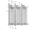
ここで、ゲート絶縁膜52a、52bから一導電型を付与する不純物元素が添加された半導体膜55を連続成膜ことが可能なプラズマCVD装置について、図10を用いて示す。図10はプラズマCVD装置の上断面を示す模式図であり、共通室1120の周りに、ロード室1110、アンロード室1115、反応室(1)〜反応室(4)1111〜1114を備えた構成となっている。共通室1120と各室の間にはゲートバルブ1122〜1127が備えられ、各室で行われる処理が、相互に干渉しないように構成されている。基板はロード室1110、アンロード室1115のカセット1128、1129に装填され、共通室1120の搬送手段1121により反応室(1)〜反応室(4)1111〜1114へ運ばれる。この装置では、堆積膜種ごとに反応室をあてがうことが可能であり、複数の異なる被膜を大気に触れさせることなく連続して形成することができる。
Here, a plasma CVD apparatus capable of continuously forming a
反応室(1)〜反応室(4)それぞれにおいて、ゲート絶縁膜52a、52b、微結晶半導体膜53、バッファ層54、及び一導電型を付与する不純物元素が添加された半導体膜55を積層形成する。この場合は、原料ガスの切り替えにより異なる種類の膜を連続的に複数積層することができる。この場合、ゲート絶縁膜を形成した後、反応室内にシラン等の水素化珪素を導入し、残留酸素及び水素化珪素を反応させて、反応物を反応室外に排出することで、反応室内の残留酸素濃度を低減させることができる。この結果、微結晶半導体膜に含まれる酸素の濃度を低減することができる。また、微結晶半導体膜に含まれる結晶粒の酸化を防止することができる。
In each of the reaction chamber (1) to the reaction chamber (4),
または、反応室(1)及び反応室(3)でゲート絶縁膜52a、52b、微結晶半導体膜53、及びバッファ層54を形成し、反応室(2)及び反応室(4)で一導電型を付与する不純物元素が添加された半導体膜55を形成する。一導電型を付与する不純物のみ単独で成膜することにより、チャンバに残存する一導電型を付与する不純物元素が他の膜に混入することを防ぐことができる。
Alternatively, the
このように、複数のチャンバが接続されたマイクロ波プラズマCVD装置で、同時にゲート絶縁膜52a、52b、微結晶半導体膜53、バッファ層54、及び一導電型を付与する不純物元素が添加された半導体膜55を成膜することができるため、量産性を高めることができる。また、ある反応室がメンテナンスやクリーニングを行っていても、残りの反応室において成膜処理が可能となり、成膜のタクトを向上させることができる。また、大気成分や大気中に浮遊する汚染不純物元素に汚染されることなく各積層界面を形成することができるので、薄膜トランジスタ特性のばらつきを低減することができる。
In this manner, in the microwave plasma CVD apparatus in which a plurality of chambers are connected, the
また、反応室(1)でゲート絶縁膜52a、52bを形成し、反応室(2)で微結晶半導体膜53及びバッファ層54を形成し、反応室(3)で一導電型を付与する不純物元素が添加された半導体膜55を形成することができる。また、ゲート絶縁膜52aを酸化珪素膜または酸化窒化珪素膜で形成し、ゲート絶縁膜52bを窒化珪素膜または窒化酸化珪素膜で形成する場合、反応室を5つ設け、反応室(1)で、ゲート絶縁膜52aの酸化珪素膜または酸化窒化珪素膜を形成し、反応室(2)で、ゲート絶縁膜52bの窒化珪素膜または窒化酸化珪素膜を形成し、反応室(3)で、微結晶半導体膜を形成し、反応室(4)でバッファ層を形成し、反応室(5)で、一導電型を付与する不純物元素が添加された半導体膜を形成してもよい。また、微結晶半導体膜は成膜速度が遅いため、複数の反応室で微結晶半導体膜を成膜してもよい。例えば、反応室(1)でゲート絶縁膜52a、52bを形成し、反応室(2)及び(3)で微結晶半導体膜53を形成し、反応室(4)でバッファ層54を形成し、反応室(5)で一導電型を付与する不純物元素が添加された半導体膜55を形成してもよい。このように、複数の反応室で同時に微結晶半導体膜53を成膜することでスループットを向上させることができる。なお、このとき、各反応室の内壁を成膜する種類の膜でコーティングすることが好ましい。
Further,
このような構成のプラズマCVD装置を用いれば、各反応室で種類の類似する膜または一種類の膜を成膜することが可能であり、且つ大気に曝すことなく連続して形成することができるため、前に成膜した膜の残留物や大気に浮遊する不純物元素に汚染されることなく、各積層界面を形成することができる。 By using the plasma CVD apparatus having such a configuration, it is possible to form a similar type film or one type of film in each reaction chamber, and to continuously form the film without exposing to the atmosphere. Therefore, each stacked interface can be formed without being contaminated by a residue of a film formed previously or an impurity element floating in the atmosphere.
なお、図10に示すプラズマCVD装置には、ロード室及びアンロード室が別々に設けられているが、一つとしロード/アンロード室とでもよい。また、プラズマCVD装置に予備室を設けてもよい。予備室で基板を予備加熱することで、各反応室において成膜までの加熱時間を短縮することが可能であるため、スループットを向上させることができる。 In the plasma CVD apparatus shown in FIG. 10, a load chamber and an unload chamber are provided separately, but a single load / unload chamber may be used. Further, a preliminary chamber may be provided in the plasma CVD apparatus. By preheating the substrate in the preliminary chamber, the heating time until film formation in each reaction chamber can be shortened, so that the throughput can be improved.
以下に、成膜処理について説明する。これらの成膜処理は、その目的に応じて、ガス供給部から供給するガスを選択すれば良い。 The film forming process will be described below. In these film forming processes, a gas supplied from a gas supply unit may be selected according to the purpose.
ここでは、ゲート絶縁膜52aに、酸化窒化珪素膜を形成し、ゲート絶縁膜52bに窒化酸化珪素膜を形成する方法を一例としてあげる。
Here, a method for forming a silicon oxynitride film on the
はじめに、マイクロ波プラズマCVD装置の反応室の処理容器の内部を、フッ素ラジカルでクリーニングする。なお、フッ素ラジカルは、反応室の外側に設けられたプラズマ発生器に、フッ化炭素、フッ化窒素、またはフッ素を導入し、解離し、フッ素ラジカルを反応室に導入することで、反応室内をクリーニングすることができる。 First, the inside of the processing chamber in the reaction chamber of the microwave plasma CVD apparatus is cleaned with fluorine radicals. Fluorine radicals are introduced into a plasma generator provided outside the reaction chamber by introducing carbon fluoride, nitrogen fluoride, or fluorine, dissociated, and introducing fluorine radicals into the reaction chamber. Can be cleaned.
フッ素ラジカルでクリーニングした後、反応室内部に水素を大量に導入することで、反応室内の残留フッ素と水素を反応させて、残留フッ素の濃度を低減することができる。このため、後に反応室の内壁に成膜する保護膜へのフッ素の混入量を減らすことが可能であり、保護膜の厚さを薄くすることが可能である。 After cleaning with fluorine radicals, a large amount of hydrogen is introduced into the reaction chamber, whereby the residual fluorine and hydrogen in the reaction chamber can be reacted to reduce the concentration of residual fluorine. For this reason, it is possible to reduce the amount of fluorine mixed into the protective film to be formed on the inner wall of the reaction chamber later, and to reduce the thickness of the protective film.
次に、反応室の処理容器内壁表面に保護膜として酸化窒化膜を堆積する。ここでは、処理容器内の圧力を1〜200Pa、好ましくは1〜100Paとし、プラズマ着火用ガスとして、ヘリウム、アルゴン、キセノン、クリプトン等の希ガスのいずれか一種以上のガスを導入する。さらには、希ガスのいずれか一種及び水素を導入する。特に、プラズマ着火用ガスとしてヘリウム、更にはヘリウムと水素を用いることが好ましい。 Next, an oxynitride film is deposited as a protective film on the inner wall surface of the processing chamber in the reaction chamber. Here, the pressure in the processing container is set to 1 to 200 Pa, preferably 1 to 100 Pa, and one or more kinds of rare gases such as helium, argon, xenon, and krypton are introduced as the plasma ignition gas. Furthermore, any one kind of rare gas and hydrogen are introduced. In particular, it is preferable to use helium, and further helium and hydrogen as the plasma ignition gas.
ヘリウムのイオン化エネルギーは24.5eVと高いエネルギーを持つが、約20eVに準安定状態があるので、放電中においては約4eVでイオン化が可能である。このため、放電開始電圧が低く、また放電を維持しやすい。よって、プラズマを均一に維持することが可能であると共に、省電力化が可能である。 Although the ionization energy of helium has a high energy of 24.5 eV, since there is a metastable state at about 20 eV, ionization is possible at about 4 eV during discharge. For this reason, the discharge start voltage is low and the discharge is easily maintained. Therefore, it is possible to maintain plasma uniformly and to save power.
また、プラズマ着火用ガスとして、ヘリウム、アルゴン、キセノン、クリプトン等の希ガスのいずれか一種以上及び酸素ガスを導入してもよい。希ガスと共に、酸素ガスを処理容器内に導入することで、プラズマの着火を容易とすることができる。 Further, as the plasma ignition gas, one or more of rare gases such as helium, argon, xenon, krypton, and oxygen gas may be introduced. By introducing oxygen gas together with the rare gas into the processing container, plasma ignition can be facilitated.
次に、電源装置の電源をオンにし、電源装置の出力は500〜6000W、好ましくは4000〜6000Wとしてプラズマを発生させる。次に、ガス供給部から原料ガスを処理容器内に導入する。具体的には、原料ガスとして、一酸化二窒素、希ガス、及びシランを導入することで、処理容器の内壁表面に保護膜として酸化窒化珪素膜を形成する。このときの水素化珪素の流量を50〜300sccm、一酸化二窒素の流量を500〜6000sccmとし、保護膜の膜厚を500〜2000nmとする。 Next, the power supply is turned on, and the output of the power supply is 500 to 6000 W, preferably 4000 to 6000 W to generate plasma. Next, the raw material gas is introduced into the processing container from the gas supply unit. Specifically, by introducing dinitrogen monoxide, a rare gas, and silane as source gases, a silicon oxynitride film is formed as a protective film on the inner wall surface of the processing container. At this time, the flow rate of silicon hydride is 50 to 300 sccm, the flow rate of dinitrogen monoxide is 500 to 6000 sccm, and the thickness of the protective film is 500 to 2000 nm.
次に、原料ガスの供給を停止し、処理容器内の圧力を低下し、電源装置の電源をオフにした後、処理容器内の支持台上に基板を導入する。 Next, the supply of the source gas is stopped, the pressure in the processing container is reduced, the power supply device is turned off, and then the substrate is introduced onto the support base in the processing container.
次に、上記保護膜と同様の工程により、基板上にゲート絶縁膜52aとして酸化窒化珪素膜を堆積させる。
Next, a silicon oxynitride film is deposited as a
所定の厚さの酸化窒化珪素膜が堆積されたら、原料ガスの供給を停止し、処理容器内の圧力を低下し、電源装置の電源をオフにする。 When the silicon oxynitride film having a predetermined thickness is deposited, the supply of the source gas is stopped, the pressure in the processing container is lowered, and the power supply device is turned off.
次に、処理容器内の圧力を1〜200Pa、好ましくは1〜100Paとし、プラズマ着火用ガスとして、ヘリウム、アルゴン、キセノン、クリプトン等の希ガスのいずれか一種以上と、原料ガスであるシラン、一酸化二窒素、及びアンモニアを導入する。なお、原料ガスとして、アンモニアの代わりに窒素を導入しても良い。次に、電源装置の電源をオンにし、電源装置の出力は500〜6000W、好ましくは4000〜6000Wとしてプラズマを発生させる。次に、ガス供給部から原料ガスを処理容器内に導入し、基板1130の酸化窒化珪素膜上にゲート絶縁膜として窒化酸化珪素膜を形成する。次に、原料ガスの供給を停止し、処理容器内の圧力を低下し、電源装置の電源をオフにして、成膜プロセスを終了する。 Next, the pressure in the processing vessel is 1 to 200 Pa, preferably 1 to 100 Pa, and as a plasma ignition gas, any one or more of noble gases such as helium, argon, xenon, krypton, and silane that is a source gas, Dinitrogen monoxide and ammonia are introduced. Note that nitrogen may be introduced instead of ammonia as the source gas. Next, the power supply is turned on, and the output of the power supply is 500 to 6000 W, preferably 4000 to 6000 W to generate plasma. Next, a source gas is introduced from the gas supply portion into the processing container, and a silicon nitride oxide film is formed as a gate insulating film over the silicon oxynitride film of the substrate 1130. Next, the supply of the source gas is stopped, the pressure in the processing container is reduced, the power supply device is turned off, and the film forming process is completed.
以上の工程により、反応室内壁の保護膜を酸化窒化珪素膜とし、基板上に酸化窒化珪素膜及び窒化酸化珪素膜を連続的に成膜することで、上層側の窒化酸化珪素膜中に酸化珪素等の不純物の混入を低減することができる。電源装置としてマイクロ波を発生させることが可能な電源装置を用いたマイクロ波プラズマCVD法により上記膜を形成することで、プラズマ密度が高くなり耐圧の高い膜を形成することができ、当該膜をゲート絶縁膜として用いると、トランジスタの閾値のばらつきを低減することができる。また、BT特性を向上させることができる。また、静電気に対する耐性が高まり、高い電圧が印加されても破壊にくいトランジスタを作製することができる。また、経時破壊の少ないトランジスタを作製することができる。また、ホットキャリアダメージの少ないトランジスタを作製することができる。 Through the above steps, the protective film on the reaction chamber wall is made of a silicon oxynitride film, and a silicon oxynitride film and a silicon nitride oxide film are continuously formed on the substrate, thereby oxidizing the silicon nitride oxide film on the upper layer side. Mixing of impurities such as silicon can be reduced. By forming the film by a microwave plasma CVD method using a power supply device capable of generating microwaves as a power supply device, a film having a high plasma density and a high withstand voltage can be formed. When used as a gate insulating film, variation in threshold values of transistors can be reduced. Moreover, BT characteristics can be improved. Further, resistance to static electricity is increased, and a transistor which is not easily broken even when a high voltage is applied can be manufactured. In addition, a transistor with little destruction with time can be manufactured. In addition, a transistor with less hot carrier damage can be manufactured.
また、ゲート絶縁膜として、マイクロ波プラズマCVD装置により形成した酸化窒化珪素膜単層の場合、上記保護膜の形成方法及び酸化窒化珪素膜の形成方法を用いる。特に、シランに対する一酸化二窒素の流量比を50倍以上300倍以下、好ましくは50倍以上250倍以下とすると、耐圧の高い酸化窒化珪素膜を形成することができる。 Further, in the case of a silicon oxynitride film single layer formed by a microwave plasma CVD apparatus as the gate insulating film, the above-described protective film formation method and silicon oxynitride film formation method are used. In particular, when the flow rate ratio of dinitrogen monoxide to silane is 50 to 300 times, preferably 50 to 250 times, a silicon oxynitride film with high withstand voltage can be formed.
次に、プラズマCVD法による微結晶半導体膜及びバッファ層として非晶質半導体膜を連続的に成膜する成膜処理方法について示す。まず、上記ゲート絶縁膜と同様により、反応室内をクリーニングする。次に、処理容器内に保護膜として珪素膜を堆積する。ここでは、処理容器内の圧力を1〜200Pa、好ましくは1〜100Paとし、プラズマ着火用ガスとして、ヘリウム、アルゴン、キセノン、クリプトン等の希ガスのいずれか一種以上を導入する。なお、希ガスと共に水素を導入してもよい。 Next, a deposition treatment method in which an amorphous semiconductor film is continuously formed as a microcrystalline semiconductor film and a buffer layer by a plasma CVD method will be described. First, the reaction chamber is cleaned in the same manner as the gate insulating film. Next, a silicon film is deposited as a protective film in the processing container. Here, the pressure in the processing container is 1 to 200 Pa, preferably 1 to 100 Pa, and any one or more of rare gases such as helium, argon, xenon, and krypton are introduced as the plasma ignition gas. Note that hydrogen may be introduced together with the rare gas.
次に、電源装置の電源をオンにし、電源装置の出力は500〜6000W、好ましくは4000〜6000Wとしてプラズマを発生させる。次に、ガス供給部から原料ガスを処理容器内に導入する。具体的には、原料ガスとして、具体的には、水素化珪素ガス、及び水素ガスを導入することで、処理容器の内壁表面に保護膜として微結晶珪素膜を形成する。また、水素化珪素ガス及び水素ガスに加え、ヘリウム、アルゴン、クリプトン、ネオンから選ばれた一種または複数種の希ガス元素で希釈して微結晶半導体膜を形成することができる。これらのときの水素化珪素に対して水素の流量比を5倍以上1000倍以下、好ましくは50倍以上200倍以下、更に好ましくは100倍以上150倍とする。また、このときの保護膜の膜厚を500〜2000nmとする。なお、電源装置の電源をオンにする前に、処理容器内に上記希ガスの他、水素化珪素ガス及び水素ガスを導入してもよい。 Next, the power supply is turned on, and the output of the power supply is 500 to 6000 W, preferably 4000 to 6000 W to generate plasma. Next, the raw material gas is introduced into the processing container from the gas supply unit. Specifically, a microcrystalline silicon film is formed as a protective film on the inner wall surface of the processing vessel by introducing silicon hydride gas and hydrogen gas as the source gas. In addition to the silicon hydride gas and the hydrogen gas, the microcrystalline semiconductor film can be formed by dilution with one or more kinds of rare gas elements selected from helium, argon, krypton, and neon. The flow rate ratio of hydrogen to silicon hydride at these times is 5 to 1000 times, preferably 50 to 200 times, more preferably 100 to 150 times. Further, the thickness of the protective film at this time is set to 500 to 2000 nm. Note that, before turning on the power supply device, a silicon hydride gas and a hydrogen gas may be introduced into the processing container in addition to the rare gas.
また、水素化珪素ガス、及び水素ガスに加え、ヘリウム、アルゴン、クリプトン、ネオンから選ばれた一種または複数種の希ガス元素で希釈して、保護膜として非晶質半導体膜を形成することができる。 In addition to silicon hydride gas and hydrogen gas, an amorphous semiconductor film may be formed as a protective film by diluting with one or more kinds of rare gas elements selected from helium, argon, krypton, and neon. it can.
次に、原料ガスの供給を停止し、処理容器内の圧力を低下し、電源装置の電源をオフにした後、処理容器内の支持台上に基板を導入する。 Next, the supply of the source gas is stopped, the pressure in the processing container is reduced, the power supply device is turned off, and then the substrate is introduced onto the support base in the processing container.
次に、基板上に形成されるゲート絶縁膜52bの表面を水素プラズマ処理してもよい。微結晶半導体膜を形成する前に水素プラズマ処理することにより、ゲート絶縁膜及び微結晶半導体膜の界面における格子歪を低減することが可能であり、ゲート絶縁膜及び微結晶半導体膜の界面特性を向上させることができる。このため、後に形成される薄膜トランジスタの電気特性を向上させることができる。
Next, the surface of the
また、上記水素プラズマ処理において、処理容器内に形成された保護膜である非晶質半導体膜または微結晶半導体膜をも水素プラズマ処理することにより、保護膜がエッチングされてゲート絶縁膜52bの表面に少量の半導体が堆積する。当該半導体が結晶成長の核となり、当該核によって、微結晶半導体膜が堆積する。この結果、ゲート絶縁膜及び微結晶半導体膜の界面における格子歪を低減することが可能であり、ゲート絶縁膜及び微結晶半導体膜の界面特性を向上させることができる。このため、後に形成される薄膜トランジスタの電気特性を向上させることができる。
In the hydrogen plasma treatment, the protective film is etched by performing hydrogen plasma treatment on the amorphous semiconductor film or the microcrystalline semiconductor film, which is a protective film formed in the processing vessel, so that the surface of the
次に、上記保護膜と同様の工程により、基板上に微結晶珪素膜を堆積させる。微結晶珪素膜の膜厚を0nmより厚く50nm以下、好ましくは0nmより厚く20nm以下とする。 Next, a microcrystalline silicon film is deposited on the substrate by the same process as the protective film. The thickness of the microcrystalline silicon film is greater than 0 nm and less than or equal to 50 nm, preferably greater than 0 nm and less than or equal to 20 nm.
所定の厚さの微結晶珪素膜が堆積されたら、次に、原料ガスの供給を停止し、処理容器内の圧力を低下し、電源装置の電源をオフにして、微結晶半導体膜成膜プロセスを終了する。 After the microcrystalline silicon film having a predetermined thickness is deposited, the supply of the raw material gas is stopped, the pressure in the processing container is lowered, the power supply device is turned off, and the microcrystalline semiconductor film forming process is performed. Exit.
次に、処理容器内の圧力を下げ、原料ガスの流量を調整する。具体的には、水素ガスの流量を微結晶半導体膜の成膜条件より大幅に低減する。代表的には、水素化珪素の流量の1倍以上20倍以下、好ましくは1倍以上10倍以下、更に好ましくは1倍以上5倍以下の流量の水素ガスを導入する。または、水素ガスを処理容器内に導入せず、水素化珪素ガスを導入する。このように水素化珪素に対する水素の流量を低減することにより、バッファ層として非晶質半導体膜の成膜速度を向上させることができる。または、水素化珪素ガスに加え、ヘリウム、アルゴン、クリプトン、ネオンから選ばれた一種または複数種の希ガス元素で希釈する。次に、電源装置の電源をオンにし、電源装置の出力は500〜6000W、好ましくは4000〜6000Wとしてプラズマ200を発生させて、非晶質半導体膜を形成することができる。非晶質半導体膜の成膜速度は微結晶半導体膜に比べて高いため、処理容器内の圧力を低く設定することができる。このときの非晶質半導体膜の膜厚を200〜400nmとする。
Next, the pressure in the processing container is lowered to adjust the flow rate of the raw material gas. Specifically, the flow rate of hydrogen gas is significantly reduced from the deposition conditions for the microcrystalline semiconductor film. Typically, hydrogen gas having a flow rate of 1 to 20 times, preferably 1 to 10 times, more preferably 1 to 5 times the flow rate of silicon hydride is introduced. Alternatively, silicon hydride gas is introduced without introducing hydrogen gas into the processing vessel. Thus, by reducing the flow rate of hydrogen with respect to silicon hydride, the deposition rate of the amorphous semiconductor film as the buffer layer can be improved. Alternatively, the silicon hydride gas is diluted with one or plural kinds of rare gas elements selected from helium, argon, krypton, and neon. Next, the power supply of the power supply device is turned on, the output of the power supply device is 500 to 6000 W, preferably 4000 to 6000 W, the
所定の厚さの非晶質半導体膜が堆積されたら、次に、原料ガスの供給を停止し、処理容器内の圧力を低下し、電源装置の電源をオフにして、非晶質半導体膜の成膜プロセスを終了する。 After the amorphous semiconductor film having a predetermined thickness is deposited, the supply of the source gas is then stopped, the pressure in the processing container is lowered, the power supply device is turned off, and the amorphous semiconductor film The film formation process is terminated.
なお、微結晶半導体膜53及びバッファ層54である非晶質半導体膜をプラズマの着火したまま形成してもよい。具体的には微結晶半導体膜53を形成する原料ガスである水素化珪素に対する水素の流量比を徐々に低減させて微結晶半導体膜53及びバッファ層54である非晶質半導体膜を積層する。このような手法により微結晶半導体膜53及びバッファ層54の界面に不純物が堆積せず、歪の少ない界面を形成することが可能であり、後に形成される薄膜トランジスタの電気特性を向上させることができる。
Note that an amorphous semiconductor film which is the
微結晶半導体膜53を形成する場合、周波数が1GHz以上のマイクロ波プラズマCVD装置を用いることが好ましい。マイクロ波プラズマは、電子密度が高く、原料ガスから多くのラジカルが形成され、基板1130へ供給されるため、基板でのラジカルの表面反応が促進され、微結晶シリコンの成膜速度を高めることができる。また、1MHzから20MHz、代表的には13.56MHzの高周波、または20MHzより大きく120MHz程度までのVHF帯の高周波、代表的には27.12MHz、60MHzを用いたプラズマCVD法により、微結晶半導体膜を形成することができる。
In the case of forming the
なお、ゲート絶縁膜及び半導体膜それぞれの作製工程において、反応室の内壁に500〜2000nmの保護膜が形成されている場合は、上記クリーニング処理及び保護膜形成処理を省くことができる。 Note that in the manufacturing process of the gate insulating film and the semiconductor film, when a protective film having a thickness of 500 to 2000 nm is formed on the inner wall of the reaction chamber, the cleaning process and the protective film forming process can be omitted.
次に、一導電型を付与する不純物元素が添加された半導体膜55上に、導電膜65a〜65cを形成する。導電膜65a〜65cは、アルミニウム、銅、若しくはシリコン、チタン、ネオジム、スカンジウム、モリブデンなどの耐熱性向上元素若しくはヒロック防止元素が添加されたアルミニウム合金の単層または積層で形成することが好ましい。また、一導電型を付与する不純物元素が添加された半導体膜と接する側の膜を、チタン、タンタル、モリブデン、タングステン、またはこれらの元素の窒化物で形成し、その上にアルミニウムまたはアルミニウム合金を形成した積層構造としても良い。更には、アルミニウムまたはアルミニウム合金の上面及び下面を、チタン、タンタル、モリブデン、タングステン、またはこれらの元素の窒化物で挟んだ積層構造としてもよい。ここでは、導電膜としては、導電膜65a〜65c3層が積層した構造の導電膜を示し、導電膜65a、65cにモリブデン膜、導電膜65bにアルミニウム膜を用いた積層導電膜や、導電膜65a、65cにチタン膜、導電膜65bにアルミニウム膜を用いた積層導電膜を示す。導電膜65a〜65cは、スパッタリング法や真空蒸着法で形成する。
Next,
レジスト80は、ポジ型レジストまたはネガ型レジストを用いることができる。ここでは、ポジ型レジストを用いて示す。 As the resist 80, a positive resist or a negative resist can be used. Here, a positive resist is used.
次に、第2のフォトマスクとして多階調マスク59を用いて、レジスト80に光を照射して、レジスト80を露光する。
Next, the resist 80 is exposed to light by irradiating the resist 80 with light using the
ここで、多階調マスク59を用いた露光について、図11を用いて説明する。
Here, exposure using the
多階調マスクとは、露光部分、中間露光部分、及び未露光部分に3つの露光レベルを行うことが可能なマスクであり、一度の露光及び現像工程により、複数(代表的には二種類)の厚さの領域を有するレジストマスクを形成することが可能である。このため、多階調マスクを用いることで、フォトマスクの枚数を削減することが可能である。 A multi-tone mask is a mask capable of performing three exposure levels on an exposed portion, an intermediate exposed portion, and an unexposed portion, and a plurality of (typically two types) can be obtained by one exposure and development process. It is possible to form a resist mask having a region with a thickness of. Therefore, the number of photomasks can be reduced by using a multi-tone mask.
多階調マスクの代表例としては、図11(A)に示すようなグレートーンマスク59a、図11(C)に示すようなハーフトーンマスク59bがある。
Typical examples of the multi-tone mask include a gray-
図11(A)に示すように、グレートーンマスク59aは、透光性を有する基板163及びその上に形成される遮光部164並びに回折格子165で構成される。遮光部164においては、光の透過率が0%である。一方、回折格子165はスリット、ドット、メッシュ等の光透過部の間隔を、露光に用いる光の解像度限界以下の間隔とすることにより、光の透過率を制御することができる。なお、回折格子165は、周期的なスリット、ドット、メッシュ、または非周期的なスリット、ドット、メッシュどちらも用いることができる。
As shown in FIG. 11A, the
透光性を有する基板163は、石英等の透光性を有する基板を用いることができる。遮光部164及び回折格子165は、クロムや酸化クロム等の光を吸収する遮光材料を用いて形成することができる。
As the
グレートーンマスク59aに露光光を照射した場合、図11(B)に示すように、遮光部164においては、光透過率166は0%であり、遮光部164及び回折格子165が設けられていない領域では光透過率166は100%である。また、回折格子165においては、10〜70%の範囲で調整可能である。回折格子165における光の透過率の調整は、回折格子のスリット、ドット、またはメッシュの間隔あるいはピッチの調整により可能である。
When the gray-
図11(C)に示すように、ハーフトーンマスク59bは、透光性を有する基板163及びその上に形成される半透過部167並びに遮光部168で構成される。半透過部167は、MoSiN、MoSi、MoSiO、MoSiON、CrSiなどを用いることができる。遮光部168は、クロムや酸化クロム等の光を吸収する遮光材料を用いて形成することができる。
As shown in FIG. 11C, the
ハーフトーンマスク59bに露光光を照射した場合、図11(D)に示すように、遮光部168においては、光透過率169は0%であり、遮光部168及び半透過部167が設けられていない領域では光透過率169は100%である。また、半透過部167においては、10〜70%の範囲で調整可能である。半透過部167に於ける光の透過率の調整は、半透過部167の材料により調整により可能である。
When the
多階調マスクを用いて露光した後、現像することで、図1(B)に示すように、膜厚の異なる領域を有するレジストマスク81を形成することができる。
By developing after exposure using a multi-tone mask, a resist
次に、レジストマスク81により、微結晶半導体膜53、バッファ層54、一導電型を付与する不純物元素が添加された半導体膜55、及び導電膜65a〜65cをエッチングし分離する。この結果、図2(A)に示すような、微結晶半導体膜61、バッファ層62、一導電型を付与する不純物元素が添加された半導体膜63、及び導電膜85a〜85cを形成することができる。なお、図2(A)は図5(A)のA−Bにおける断面図に相当する(但しレジストマスク86を除く)。
Next, the
微結晶半導体膜61、バッファ層62の端部側面が傾斜していることにより、バッファ層62上に形成されるソース領域及びドレイン領域と微結晶半導体膜61との間にリーク電流が生じること防止することが可能である。また、ソース電極及びドレイン電極と、微結晶半導体膜61との間にリーク電流が生じるのを防止することが可能である。微結晶半導体膜61及びバッファ層62の端部側面の傾斜角度は、30°〜90°、好ましくは45°〜80°である。このような角度とすることで、段差形状によるソース電極またはドレイン電極の段切れを防ぐことができる。
Since the side surfaces of the end portions of the
次に、レジストマスク81をアッシングする。この結果、レジストの面積が縮小し、厚さが薄くなる。このとき、膜厚の薄い領域のレジスト(ゲート電極51の一部と重畳する領域)は除去され、図6(B)に示すように、分離されたレジストマスク86を形成することができる。
Next, the resist
次に、レジストマスク86を用いて一導電型を付与する不純物元素が添加された半導体膜63、及び導電膜85a〜85cをエッチングし分離する。ここでは、ドライエッチングにより、導電膜85a〜85cを分離する。この結果、図2(B)に示すような、一対の導電膜89a〜89c、及び一対のソース領域及びドレイン領域89を形成することができる。なお、当該エッチング工程において、バッファ層62の一部もエッチングする。一部エッチングされたバッファ層をバッファ層88と示す。ソース領域及びドレイン領域の形成工程と、バッファ層の凹部とを同一工程で形成することができる。ここでは、バッファ層88の一部が、面積が縮小したレジストマスク86で一部エッチングされたため、導電膜85a〜85cの外側にバッファ層88が突出した形状となる。
Next, the
次に、図2(C)に示すように、導電膜89a〜89cの一部をエッチングしソース電極及びドレイン電極92a〜92cを形成する。ここでは、レジストマスク86を用いて導電膜89a〜89cをウエットエッチングすると、導電膜89a〜89cの端部が選択的にエッチングされる。この結果、レジストマスク86及び導電膜89a〜89cより面積の小さいソース電極及びドレイン電極92a〜92cを形成することができる。ソース電極及びドレイン電極92a〜92cの端部と、ソース領域及びドレイン領域89の端部は一致せずずれており、ソース電極及びドレイン電極92a〜92cの端部の外側に、ソース領域及びドレイン領域89の端部が形成される。この後、レジストマスク86を除去する。
Next, as illustrated in FIG. 2C, part of the
なお、図2(C)は、図5(B)のA−Bの断面図に相当する。図5(B)に示すように、ソース領域及びドレイン領域89の端部は、ソース電極及びドレイン電極92cの端部の外側に位置することが分かる。また、バッファ層88の端部はソース電極及びドレイン電極92c及びソース領域及びドレイン領域89の端部の外側に位置する。また、ソース電極及びドレイン電極の一方はソース領域及びドレイン領域の他方を部分的に囲む形状(具体的には、U字型、C字型)である。このため、キャリアが移動する領域の面積を増加させることが可能であるため、電流量を増やすことが可能であり、薄膜トランジスタの面積を縮小することができる。また、ゲート電極の内側において、微結晶半導体膜87、ソース電極及びドレイン電極92cが重畳されているため、ゲート電極の端部における凹凸の影響が少なく、被覆率の低減及びリーク電流の発生を抑制することができる。なお、ソース電極またはドレイン電極の一方は、ソース配線またはドレイン配線としても機能する。
Note that FIG. 2C corresponds to a cross-sectional view taken along a line AB in FIG. As shown in FIG. 5B, it can be seen that the ends of the source and drain
図2(C)に示すように、ソース電極及びドレイン電極92a〜92cの端部と、ソース領域及びドレイン領域89の端部は一致せずずれた形状となることで、ソース電極及びドレイン電極92a〜92cの端部の距離が離れるため、ソース電極及びドレイン電極間のリーク電流やショートを防止することができる。このため、信頼性が高く、且つ耐圧の高い薄膜トランジスタを作製することができる。
As shown in FIG. 2C, the end portions of the source and
以上の工程により、チャネルエッチ型の薄膜トランジスタ83を形成することができる。また、2枚のフォトマスクを用いて薄膜トランジスタを形成することができる。
Through the above process, a channel-etched
本実施の形態で示す薄膜トランジスタは、ゲート電極上にゲート絶縁膜、微結晶半導体膜、バッファ層、ソース領域及びドレイン領域、ソース電極及びドレイン電極が積層され、チャネル形成領域として機能する微結晶半導体膜の表面をバッファ層が覆う。また、バッファ層の一部には凹部(溝)が形成されており、当該凹部以外の領域がソース領域及びドレイン領域で覆われる。即ち、バッファ層に形成される凹部により、ソース領域及びドレイン領域の間のキャリアが移動する距離が長いため、ソース領域及びドレイン領域の間でのリーク電流を低減することができる。また、バッファ層の一部をエッチングすることにより凹部を形成するため、ソース領域及びドレイン領域の形成工程において発生するエッチング残渣を除去することができるため、残渣を介してソース領域及びドレイン領域にリーク電流(寄生チャネル)が発生することを回避することができる。 In the thin film transistor described in this embodiment, a gate insulating film, a microcrystalline semiconductor film, a buffer layer, a source region and a drain region, a source electrode and a drain electrode are stacked over a gate electrode, and the microcrystalline semiconductor film functions as a channel formation region A buffer layer covers the surface. In addition, a recess (groove) is formed in a part of the buffer layer, and regions other than the recess are covered with the source region and the drain region. That is, the distance that carriers move between the source region and the drain region due to the recess formed in the buffer layer is long, so that leakage current between the source region and the drain region can be reduced. In addition, since the recess is formed by etching a part of the buffer layer, etching residues generated in the process of forming the source region and the drain region can be removed, so that leakage occurs in the source region and the drain region through the residue. Generation of a current (parasitic channel) can be avoided.
また、チャネル形成領域として機能する微結晶半導体膜とソース領域及びドレイン領域との間に、バッファ層が形成されている。また、微結晶半導体膜の表面がバッファ層で覆われている。高抵抗率の非晶質半導体膜で形成されたバッファ層は、微結晶半導体膜と、ソース領域及びドレイン領域との間にまで延在しているため、薄膜トランジスタがオフの場合(即ち、ゲート電圧を負の電圧とした場合)の、リーク電流を低減することができると共に、高い電圧の印加による劣化を低減することができる。また、微結晶半導体膜の表面に水素で表面が終端された非晶質半導体膜がバッファ層として形成されているため、微結晶半導体膜の酸化を防止することが可能であると共に、ソース領域及びドレイン領域の形成工程に発生するエッチング残渣が微結晶半導体膜に混入することを防ぐことができる。このため、電気特性が高く、且つドレイン耐圧に優れた薄膜トランジスタである。 In addition, a buffer layer is formed between the microcrystalline semiconductor film functioning as a channel formation region and the source and drain regions. In addition, the surface of the microcrystalline semiconductor film is covered with a buffer layer. Since the buffer layer formed of a high resistivity amorphous semiconductor film extends between the microcrystalline semiconductor film and the source and drain regions, the thin film transistor is turned off (that is, the gate voltage). Leakage current when the voltage is negative), and deterioration due to application of a high voltage can be reduced. Further, since the amorphous semiconductor film whose surface is terminated with hydrogen is formed as a buffer layer on the surface of the microcrystalline semiconductor film, the microcrystalline semiconductor film can be prevented from being oxidized, and the source region and Etching residues generated in the drain region formation step can be prevented from entering the microcrystalline semiconductor film. Therefore, the thin film transistor has high electrical characteristics and excellent drain breakdown voltage.
また、ソース電極及びドレイン電極の端部と、ソース領域及びドレイン領域の端部は一致せずずれた形状となることで、ソース電極及びドレイン電極の端部の距離が離れるため、ソース電極及びドレイン電極間のリーク電流やショートを防止することができる。 In addition, since the end portions of the source electrode and the drain electrode and the end portions of the source region and the drain region are not aligned and shifted, the distance between the end portions of the source electrode and the drain electrode is increased. Leakage current between electrodes and short circuit can be prevented.
次に、図3(A)に示すように、ソース電極及びドレイン電極92a〜92c、ソース領域及びドレイン領域89、バッファ層88、微結晶半導体膜87、及びゲート絶縁膜52b上に絶縁膜76を形成する。絶縁膜76は、ゲート絶縁膜52a、52bと同様に形成することができる。なお、絶縁膜76は、大気中に浮遊する有機物や金属物、水蒸気などの汚染不純物の侵入を防ぐためのものであり、緻密な膜が好ましい。また、絶縁膜76に窒化珪素膜を用いることで、バッファ層88中の酸素濃度を5×10¹⁹atoms/cm3以下、好ましくは1×1019atoms/cm3以下とすることができる。
Next, as illustrated in FIG. 3A, an insulating
次に、絶縁膜76にコンタクトホールを形成し、当該コンタクトホールにおいてソース電極またはドレイン電極92cに接する画素電極77を形成する。なお、図3(B)は、図5(C)のA−Bの断面図に相当する。
Next, a contact hole is formed in the insulating
画素電極77は、酸化タングステンを含むインジウム酸化物、酸化タングステンを含むインジウム亜鉛酸化物、酸化チタンを含むインジウム酸化物、酸化チタンを含むインジウム錫酸化物、インジウム錫酸化物(以下、ITOと示す。)、インジウム亜鉛酸化物、酸化ケイ素を添加したインジウム錫酸化物などの透光性を有する導電性材料を用いることができる。
The
また、画素電極77として、導電性高分子(導電性ポリマーともいう)を含む導電性組成物を用いて形成することができる。導電性組成物を用いて形成した画素電極は、シート抵抗が10000Ω/□以下、波長550nmにおける透光率が70%以上であることが好ましい。また、導電性組成物に含まれる導電性高分子の抵抗率が0.1Ω・cm以下であることが好ましい。
The
導電性高分子としては、いわゆるπ電子共役系導電性高分子が用いることができる。例えば、ポリアニリンまたはその誘導体、ポリピロールまたはその誘導体、ポリチオフェンまたはその誘導体、若しくはこれらの2種以上の共重合体などがあげられる。 As the conductive polymer, a so-called π-electron conjugated conductive polymer can be used. For example, polyaniline or a derivative thereof, polypyrrole or a derivative thereof, polythiophene or a derivative thereof, or a copolymer of two or more kinds thereof can be given.
以上により液晶表示装置に用いることが可能な素子基板を形成することができる。 Thus, an element substrate that can be used for a liquid crystal display device can be formed.
なお、図2(A)に示すように、微結晶半導体膜61、バッファ層62、一導電型を付与する不純物元素が添加された半導体膜63、及び導電膜85a〜85cを形成した後、図4(A)に示すように、レジストマスク86を用いて導電膜85a〜85cをエッチングする。ここでは、レジストマスク86を用いて導電膜85a〜85cをウエットエッチングにより等方的にエッチングすると、導電膜85a〜85cが選択的にエッチングされる。この結果、レジストマスク86より面積の小さいソース電極及びドレイン電極92a〜92cを形成することができる。
2A, after the
次に、図4(B)に示すように、レジストマスク86を用いて一導電型を付与する不純物元素が添加された半導体膜63をエッチングする。ここでは、ドライエッチングにより一導電型を付与する不純物元素が添加された半導体膜63を異方的にエッチングすると、レジストマスク86と同程度の面積のソース領域及びドレイン領域89を形成することができる。
Next, as illustrated in FIG. 4B, the
ソース電極及びドレイン電極92a〜92cの端部と、ソース領域及びドレイン領域89の端部は一致せずずれた形状となることで、ソース電極及びドレイン電極92a〜92cの端部の距離が離れるため、ソース電極及びドレイン電極間のリーク電流やショートを防止することができる。このため、信頼性が高く、且つ耐圧の高い薄膜トランジスタを作製することができる。
Since the end portions of the source and
図1乃至図4に示すように、ウエットエッチングで導電膜をエッチングし、ドライエッチングで一導電型を付与する不純物元素が添加された半導体膜をエッチングすることで、少ないフォトマスク数でソース電極及びドレイン電極の端部と、ソース領域及びドレイン領域の端部が一致せず、異なる構造にすることができる。 As shown in FIGS. 1 to 4, the conductive film is etched by wet etching, and the semiconductor film to which the impurity element imparting one conductivity type is added is etched by dry etching. The ends of the drain electrode and the ends of the source region and the drain region do not coincide with each other, so that different structures can be obtained.
次に、上記形態とは異なる薄膜トランジスタの作製方法について、図6乃至図9を用いて説明する。ここでは、ソース電極またはドレイン電極と、ソース配線またはドレイン配線とが異なる形態について以下に示す。 Next, a method for manufacturing a thin film transistor, which is different from the above mode, is described with reference to FIGS. Here, modes in which a source electrode or a drain electrode is different from a source wiring or a drain wiring are described below.
図6(A)に示すように、基板50上にゲート電極51を形成する。次に、ゲート電極51上に、ゲート絶縁膜52a、52b、微結晶半導体膜53、バッファ層54、一導電型を付与する不純物元素が添加された半導体膜55、及び導電膜65aを順に形成する。次に、導電膜65a上にレジストを塗布し、図1(A)に示す多階調マスクを用いて厚さの異なる領域を有するレジストマスク81を形成する。
As shown in FIG. 6A, a
次に、レジストマスク81により、微結晶半導体膜53、バッファ層54、一導電型を付与する不純物元素が添加された半導体膜55、及び導電膜65aをエッチングし分離する。この結果、図6(B)に示すような、微結晶半導体膜61、バッファ層62、一導電型を付与する不純物元素が添加された半導体膜63、及び導電膜85aを形成する。なお、図6(B)は図9(A)のA−Bにおける断面図に相当する(但しレジストマスク86を除く)。
Next, with the resist
次に、レジストマスク81をアッシングして分離されたレジストマスク86を形成する。次に、レジストマスク86を用いて一導電型を付与する不純物元素が添加された半導体膜63、及び導電膜85aをエッチングし分離する。この結果、図6(C)に示すような、一対の導電膜89a、及び一対のソース領域及びドレイン領域89を形成することができる。なお、当該エッチング工程において、バッファ層62の一部もエッチングする。一部エッチングされたバッファ層をバッファ層88と示す。ここでは、バッファ層88の一部が、面積が縮小したレジストマスク86で一部エッチングされたため、導電膜85aの外側にバッファ層88が突出した形状となる。本実施の形態に示すように、バッファ層の側面において、階段状になっているため、後に形成される絶縁膜の被覆率が高まる。このため、絶縁膜上に形成される画素電極と、薄膜トランジスタとの間におけるリーク電流を低減することができる。
Next, the resist
次に、レジストマスク86をアッシングする。この結果、図7(A)に示すように、レジストマスクの面積が縮小し、厚さが薄くなる。次にアッシングされたレジストマスク91を用いて導電膜89aの一部をエッチングすることで、図7(B)に示すように、ソース電極及びドレイン電極92aを形成する。ソース電極及びドレイン電極92aの端部と、ソース領域及びドレイン領域89の端部は一致せずずれる。ここでは、レジストマスク91を用いてドライエッチングにより導電膜89aの露出部を異方的にエッチングする。この後、レジストマスク91を除去する。
Next, the resist
この結果、導電膜89aより面積の小さいソース電極及びドレイン電極92aを形成する。この後、レジストマスク91を除去する。なお、図7(B)は、図9(B)のA−Bの断面図に相当する。図9(B)に示すように、ソース領域及びドレイン領域89の端部は、ソース電極及びドレイン電極92aの端部の外側に位置することが分かる。また、バッファ層88の端部は、ソース電極及びドレイン電極92a、並びにソース領域及びドレイン領域89の外側に位置する。また、ソース電極及びドレイン電極92aはそれぞれ分離されていて、隣接する画素に形成される電極と接続していない。なお、ここでは、レジストマスク86をアッシングして形成したレジストマスク91を用いてソース電極及びドレイン電極92aを形成したが、図1乃至図4に示す工程に示すように、レジストマスク86を用いてウエットエッチングしてソース電極及びドレイン電極92a〜92cを形成してもよい。
As a result, the source and
図7(B)に示すように、ソース電極及びドレイン電極92aの端部と、ソース領域及びドレイン領域89の端部は一致せずずれた形状となることで、ソース電極及びドレイン電極92aの端部の距離が離れるため、ソース電極及びドレイン電極間のリーク電流やショートを防止することができる。このため、信頼性が高く、且つ耐圧の高い薄膜トランジスタを作製することができる。
As shown in FIG. 7B, the ends of the source and
次に、図7(C)に示すように、ソース電極及びドレイン電極92a、ソース領域及びドレイン領域89、バッファ層88、及びゲート絶縁膜52b上に絶縁膜76を形成する。絶縁膜76は、ゲート絶縁膜52a、52bと同様に形成することができる。
Next, as illustrated in FIG. 7C, the insulating
次に、図8(A)に示すように、絶縁膜76にコンタクトホールを形成し、当該コンタクトホールにおいてソース電極またはドレイン電極92aの一方に接し、且つ積層された配線93b、93cを形成する。なお、図8(A)は、図9(C)のA−Bの断面図に相当する。また、配線93b、93cは、隣接する画素に形成されるソース電極またはドレイン電極を接続する配線である。
Next, as illustrated in FIG. 8A, a contact hole is formed in the insulating
次に、図8(B)に示すように、次に、コンタクトホールにおいてソース電極またはドレイン電極92aの他方に接する画素電極77を形成する。なお、図8(B)は、図9(D)のA−Bの断面図に相当する。
Next, as shown in FIG. 8B, next, a
以上の工程により、チャネルエッチ型の薄膜トランジスタ84を形成することができる。チャネルエッチ型の薄膜トランジスタは、作製工程数が少なく、コスト削減が可能である。また、微結晶半導体膜でチャネル形成領域を構成することにより1〜20cm2/V・secの電界効果移動度を得ることができる。従って、この薄膜トランジスタを画素部の画素のスイッチング用素子として、さらに走査線(ゲート線)側の駆動回路を形成する素子として利用することができる。
Through the above process, a channel-etched
本実施の形態により、電気特性の信頼性の高い薄膜トランジスタを作製することができる。 According to this embodiment mode, a thin film transistor with high reliability in electrical characteristics can be manufactured.
(実施の形態2)
本実施の形態では、実施の形態1で示す薄膜トランジスタを有する液晶表示装置について、以下に示す。
(Embodiment 2)
In this embodiment, a liquid crystal display device including the thin film transistor described in
はじめにVA(Vertical Alignment)型の液晶表示装置について示す。VA型の液晶表示装置とは、液晶パネルの液晶分子の配列を制御する方式の一種である。VA型の液晶表示装置は、電圧が印加されていないときにパネル面に対して液晶分子が垂直方向を向く方式である。本実施の形態では、特に画素(ピクセル)をいくつかの領域(サブピクセル)に分け、それぞれ別の方向に分子を倒すよう工夫されている。これをマルチドメイン化あるいはマルチドメイン設計という。以下の説明では、マルチドメイン設計が考慮された液晶表示装置について説明する。 First, a VA (vertical alignment) liquid crystal display device is described. The VA liquid crystal display device is a type of a method for controlling the alignment of liquid crystal molecules in a liquid crystal panel. The VA liquid crystal display device is a method in which liquid crystal molecules face a vertical direction with respect to a panel surface when no voltage is applied. In the present embodiment, the pixel (pixel) is divided into several regions (sub-pixels), and each molecule is devised to tilt the molecules in different directions. This is called multi-domain or multi-domain design. In the following description, a liquid crystal display device considering multi-domain design will be described.
図16及び図17は、それぞれ画素電極及び対向電極を示している。なお、図16は画素電極が形成される基板側の平面図であり、図中に示す切断線A−Bに対応する断面構造を図15に表している。また、図17は対向電極が形成される基板側の平面図である。以下の説明ではこれらの図を参照して説明する。 16 and 17 show a pixel electrode and a counter electrode, respectively. 16 is a plan view of the substrate side on which the pixel electrode is formed, and FIG. 15 shows a cross-sectional structure corresponding to the cutting line AB shown in the drawing. FIG. 17 is a plan view of the substrate side on which the counter electrode is formed. The following description will be given with reference to these drawings.
図15は、TFT628とそれに接続する画素電極624、及び保持容量部630が形成された基板600と、対向電極640等が形成される対向基板601とが重ね合わせられ、液晶が注入された状態を示している。
FIG. 15 illustrates a state in which a liquid crystal is injected by superimposing a
対向基板601においてスペーサ642が形成される位置には、遮光膜632、第1の着色膜634、第2の着色膜636、第3着色膜638、対向電極640が形成されている。この構造により、液晶の配向を制御するための突起644とスペーサ642の高さを異ならせている。画素電極624上には配向膜648が形成され、同様に対向電極640上にも配向膜646が形成されている。この間に液晶層650が形成されている。
A
スペーサ642はここでは柱状スペーサを用いて示したがビーズスペーサを散布してもよい。さらには、スペーサ642を基板600上に形成される画素電極624上に形成してもよい。
The
基板600上には、TFT628とそれに接続する画素電極624、及び保持容量部630が形成される。画素電極624は、TFT628、配線、及び保持容量部630を覆う絶縁膜620、絶縁膜620を覆う絶縁膜622をそれぞれ貫通するコンタクトホール623で、配線618と接続する。TFT628は実施の形態1で示す薄膜トランジスタを適宜用いることができる。また、保持容量部630は、TFT628のゲート配線602と同様に形成した第1の容量配線604と、ゲート絶縁膜606と、配線616、618と同様に形成した第2の容量配線617で構成される。
A
画素電極624と液晶層650と対向電極640が重なり合うことで、液晶素子が形成されている。
The
図16に基板600上の構造を示す。画素電極624は実施の形態1で示した材料を用いて形成する。画素電極624にはスリット625を設ける。スリット625は液晶の配向を制御するためのものである。
FIG. 16 shows a structure on the
図16に示すTFT629とそれに接続する画素電極626及び保持容量部631は、それぞれTFT628、画素電極624及び保持容量部630と同様に形成することができる。TFT628とTFT629は共に配線616と接続している。この液晶パネルの画素(ピクセル)は、画素電極624と画素電極626により構成されている。画素電極624と画素電極626はサブピクセルである。
The
図17に対向基板側の構造を示す。遮光膜632上に対向電極640が形成されている。対向電極640は、画素電極624と同様の材料を用いて形成することが好ましい。対向電極640上には液晶の配向を制御する突起644が形成されている。また、遮光膜632の位置に合わせてスペーサ642が形成されている。
FIG. 17 shows a structure on the counter substrate side. A
この画素構造の等価回路を図18に示す。TFT628とTFT629は、共にゲート配線602、配線616と接続している。この場合、容量配線604と容量配線605の電位を異ならせることで、液層素子651と液晶素子652の動作を異ならせることができる。すなわち、容量配線604と容量配線605の電位を個別に制御することにより液晶の配向を精密に制御して視野角を広げている。
An equivalent circuit of this pixel structure is shown in FIG. The
スリット625を設けた画素電極624に電圧を印加すると、スリット625の近傍には電界の歪み(斜め電界)が発生する。このスリット625と、対向基板601側の突起644とを交互に咬み合うように配置することで、斜め電界が効果的に発生させて液晶の配向を制御することで、液晶が配向する方向を場所によって異ならせている。すなわち、マルチドメイン化して液晶パネルの視野角を広げている。
When a voltage is applied to the
次に、上記とは異なるVA型の液晶表示装置について、図19乃至図22を用いて説明する。 Next, a VA liquid crystal display device different from the above is described with reference to FIGS.
図19と図20は、VA型液晶パネルの画素構造を示している。図20は基板600の平面図であり、図中に示す切断線Y−Zに対応する断面構造を図19に表している。以下の説明ではこの両図を参照して説明する。
19 and 20 show a pixel structure of a VA liquid crystal panel. FIG. 20 is a plan view of the
この画素構造は、一つの画素に複数の画素電極が有り、それぞれの画素電極にTFTが接続されている。各TFTは、異なるゲート信号で駆動されるように構成されている。すなわち、マルチドメイン設計された画素において、個々の画素電極に印加する信号を、独立して制御する構成を有している。 In this pixel structure, a single pixel has a plurality of pixel electrodes, and a TFT is connected to each pixel electrode. Each TFT is configured to be driven by a different gate signal. In other words, a multi-domain designed pixel has a configuration in which signals applied to individual pixel electrodes are controlled independently.
画素電極624はコンタクトホール623において、配線618を用いてTFT628と接続している。また、画素電極626はコンタクトホール627において、配線619を用いてTFT629と接続している。TFT628のゲート配線602と、TFT629のゲート配線603には、異なるゲート信号を与えることができるように分離されている。一方、データ線として機能する配線616は、TFT628とTFT629で共通に用いられている。また、容量配線690、ゲート絶縁膜606、及び配線618で第1の容量素子を形成し、容量配線690、ゲート絶縁膜606、及び配線619で第2の容量素子を形成する。TFT628とTFT629は実施の形態1で示す薄膜トランジスタを適宜用いることができる。
The
画素電極624と画素電極626の形状は異なっており、スリット625によって分離されている。V字型に広がる画素電極624の外側を囲むように画素電極626が形成されている。画素電極624と画素電極626に印加する電圧のタイミングを、TFT628及びTFT629により異ならせることで、液晶の配向を制御している。この画素構造の等価回路を図22に示す。TFT628はゲート配線602と接続し、TFT629はゲート配線603と接続している。ゲート配線602とゲート配線603は異なるゲート信号を与えることで、TFT628とTFT629の動作タイミングを異ならせることができる。
The
対向基板601には、遮光膜632、第2の着色膜636、対向電極640が形成されている。また、第2の着色膜636と対向電極640の間には平坦化膜637が形成され、液晶の配向乱れを防いでいる。図21に対向基板側の構造を示す。対向電極640は異なる画素間で共通化されている電極であるが、スリット641が形成されている。このスリット641と、画素電極624及び画素電極626側のスリット625とを交互に咬み合うように配置することで、斜め電界が効果的に発生させて液晶の配向を制御することができる。これにより、液晶が配向する方向を場所によって異ならせることができ、視野角を広げている。
A
画素電極624と液晶層650と対向電極640が重なり合うことで、第1の液晶素子が形成されている。また、画素電極626と液晶層650と対向電極640が重なり合うことで、第2の液晶素子が形成されている。また、一画素に第1の液晶素子と第2の液晶素子が設けられたマルチドメイン構造である。
The
次に、横電界方式の液晶表示装置について示す。横電界方式は、セル内の液晶分子に対して水平方向に電界を加えることで液晶を駆動して階調表現する方式である。この方式によれば、視野角を約180度にまで広げることができる。以下の説明では、横電界方式を採用する液晶表示装置について説明する。 Next, a horizontal electric field liquid crystal display device is described. The horizontal electric field method is a method of expressing gradation by driving a liquid crystal by applying an electric field in a horizontal direction to liquid crystal molecules in a cell. According to this method, the viewing angle can be expanded to about 180 degrees. In the following description, a liquid crystal display device adopting a horizontal electric field method will be described.
図23は、TFT628とそれに接続する画素電極624が形成された基板600と、対向基板601を重ね合わせ、液晶を注入した状態を示している。対向基板601には遮光膜632、第2の着色膜636、平坦化膜637などが形成されている。画素電極は基板600側に有るので、対向基板601側には設けられていない。基板600と対向基板601の間に液晶層650が形成されている。
FIG. 23 shows a state in which the
基板600上には、第1の画素電極607及び第1の画素電極607に接続する容量配線604、及び実施の形態1で示すTFT628が形成される。第1の画素電極607は、実施の形態1で示す画素電極77と同様の材料を用いることができる。また、第1の画素電極607は略画素の形状に区画化した形状で形成する。なお、第1の画素電極607及び容量配線604上にはゲート絶縁膜606が形成される。
Over the
TFT628の配線616、配線618がゲート絶縁膜606上に形成される。配線616は液晶パネルにおいてビデオ信号をのせるデータ線であり一方向に伸びる配線であると同時に、ソース領域610と接続し、ソース及びドレインの一方の電極となる。配線618はソース及びドレインの他方の電極となり、第2の画素電極624と接続する配線である。
A
配線616、配線618上に絶縁膜620が形成される。また、絶縁膜620上には、絶縁膜620に形成されるコンタクトホール623において、配線618に接続する第2の画素電極624が形成される。画素電極624は実施の形態1で示した画素電極77と同様の材料を用いて形成する。
An insulating
このようにして、基板600上にTFT628とそれに接続する第2の画素電極624が形成される。なお、保持容量は第1の画素電極607と第2の画素電極624の間で形成している。
In this manner, the
図24は、画素電極の構成を示す平面図である。画素電極624にはスリット625が設けられる。スリット625は液晶の配向を制御するためのものである。この場合、電界は第1の画素電極607と第2の画素電極624の間で発生する。第1の画素電極607と第2の画素電極624の間にはゲート絶縁膜606が形成されているが、ゲート絶縁膜606の厚さは50〜200nmであり、2〜10μmである液晶層の厚さと比較して十分薄いので、実質的に基板600と平行な方向(水平方向)に電界が発生する。この電界により液晶の配向が制御される。この基板と略平行な方向の電界を利用して液晶分子を水平に回転させる。この場合、液晶分子はどの状態でも水平であるため、見る角度によるコントラストなどの影響は少なく、視野角が広がることとなる。また、第1の画素電極607と第2の画素電極624は共に透光性の電極であるので、開口率を向上させることができる。
FIG. 24 is a plan view showing the configuration of the pixel electrode. The
次に、横電界方式の液晶表示装置の他の一例について示す。 Next, another example of a horizontal electric field liquid crystal display device is described.
図25と図26は、IPS型の液晶表示装置の画素構造を示している。図26は平面図であり、図中に示す切断線A−Bに対応する断面構造を図25に表している。以下の説明ではこの両図を参照して説明する。 25 and 26 show a pixel structure of an IPS liquid crystal display device. FIG. 26 is a plan view, and FIG. 25 shows a cross-sectional structure corresponding to the cutting line AB shown in the figure. The following description will be given with reference to both the drawings.
図25は、TFT628とそれに接続する画素電極624が形成された基板600と、対向基板601を重ね合わせ、液晶を注入した状態を示している。対向基板601には遮光膜632、第2の着色膜636、平坦化膜637などが形成されている。画素電極は基板600側にあるので、対向基板601側には設けられていない。基板600と対向基板601の間に液晶層650が形成されている。
FIG. 25 shows a state in which the
基板600上には、共通電位線609、及び実施の形態1で示すTFT628が形成される。共通電位線609は薄膜トランジスタ628のゲート配線602と同時に形成することができる。
Over the
TFT628の配線616、配線618がゲート絶縁膜606上に形成される。配線616は液晶パネルにおいてビデオ信号をのせるデータ線であり一方向に伸びる配線であると同時に、ソース領域610と接続し、ソース及びドレインの一方の電極となる。配線618はソース及びドレインの他方の電極となり、第2の画素電極624と接続する配線である。
A
配線616、配線618上に第2の絶縁膜620が形成される。また、絶縁膜620上には、絶縁膜620に形成されるコンタクトホール623において、配線618に接続する画素電極624が形成される。画素電極624は実施の形態1で示した画素電極77と同様の材料を用いて形成する。なお、図26に示すように、画素電極624は、共通電位線609と同時に形成した櫛形の電極と横電界が発生するように形成される。また、画素電極624の櫛歯の部分が共通電位線609と同時に形成した櫛形の電極と交互に咬み合うように形成される。
A second
画素電極624に印加される電位と共通電位線609の電位との間に電界が生じると、この電界により液晶の配向が制御される。この基板と略平行な方向の電界を利用して液晶分子を水平に回転させる。この場合、液晶分子はどの状態でも水平であるため、見る角度によるコントラストなどの影響は少なく、視野角が広がることとなる。
When an electric field is generated between the potential applied to the
このようにして、基板600上にTFT628とそれに接続する画素電極624が形成される。保持容量は共通電位線609と容量電極615の間にゲート絶縁膜606を設け、それにより形成している。容量電極615と画素電極624はコンタクトホール633を介して接続されている。
In this manner, the
次に、TN型の液晶表示装置の形態について示す。 Next, a form of a TN liquid crystal display device is described.
図27と図28は、TN型の液晶表示装置の画素構造を示している。図28は平面図であり、図中に示す切断線A−Bに対応する断面構造を図27に表している。以下の説明ではこの両図を参照して説明する。 27 and 28 show a pixel structure of a TN liquid crystal display device. FIG. 28 is a plan view, and FIG. 27 shows a cross-sectional structure corresponding to the cutting line AB in the drawing. The following description will be given with reference to both the drawings.
画素電極624はコンタクトホール623により、配線618でTFT628と接続している。データ線として機能する配線616は、TFT628と接続している。TFT628は実施の形態1に示すTFTのいずれかを適用することができる。
The
画素電極624は、実施の形態1で示す画素電極77を用いて形成されている。
The
対向基板601には、遮光膜632、第2の着色膜636、対向電極640が形成されている。また、第2の着色膜636と対向電極640の間には平坦化膜637が形成され、液晶の配向乱れを防いでいる。液晶層650は画素電極624と対向電極640の間に形成されている。
A
画素電極624と液晶層650と対向電極640が重なり合うことで、液晶素子が形成されている。
The
対向電極640は、画素電極624と同様の材料を適宜用いることができる。画素電極624と液晶層650と対向電極640が重なり合うことで、液晶素子が形成されている。
The
また、図15乃至図28に示す液晶表示装置において、基板600または対向基板601にカラーフィルタや、ディスクリネーションを防ぐための遮蔽膜(ブラックマトリクス)などが形成されていても良い。また、基板600の薄膜トランジスタが形成されている面とは逆の面に偏光板を貼り合わせ、また対向基板601の対向電極640が形成されている面とは逆の面に、偏光板を貼り合わせておく。
In the liquid crystal display device illustrated in FIGS. 15 to 28, a color filter, a shielding film (black matrix) for preventing disclination, or the like may be formed over the
以上の工程により、液晶表示装置を作製することができる。本実施の形態の液晶表示装置は、オフ電流が少なく、電気特性の信頼性の高い薄膜トランジスタを用いているため、コントラストが高く、視認性の高い液晶表示装置である。また、レーザ結晶化工程のない微結晶半導体膜をチャネル形成領域に用いた薄膜トランジスタを用いているため、視認性の高い液晶表示装置を量産高く作製することができる。 Through the above process, a liquid crystal display device can be manufactured. The liquid crystal display device in this embodiment is a liquid crystal display device with high contrast and high visibility because a thin film transistor with low off-state current and high electrical characteristics is used. In addition, since a thin film transistor in which a microcrystalline semiconductor film without a laser crystallization process is used for a channel formation region, a highly visible liquid crystal display device can be manufactured with high mass production.
(実施の形態3)
次に、本発明の液晶表示装置の一形態である表示パネルの構成について、以下に示す。
(Embodiment 3)
Next, a structure of a display panel which is one embodiment of the liquid crystal display device of the present invention is described below.
図12(A)に、信号線駆動回路6013のみを別途形成し、基板6011上に形成された画素部6012と接続している表示パネルの形態を示す。画素部6012及び走査線駆動回路6014は、微結晶半導体膜をチャネル形成領域に用いた薄膜トランジスタを用いて形成する。微結晶半導体膜をチャネル形成領域に用いた薄膜トランジスタよりも高い電界効果移動が得られるトランジスタで信号線駆動回路を形成することで、走査線駆動回路よりも高い駆動周波数が要求される信号線駆動回路の動作を安定させることができる。なお、信号線駆動回路6013は、単結晶の半導体をチャネル形成領域に用いたトランジスタ、多結晶の半導体をチャネル形成領域に用いた薄膜トランジスタ、またはSOIを用いたトランジスタであっても良い。画素部6012と、信号線駆動回路6013と、走査線駆動回路6014とに、それぞれ電源の電位、各種信号等が、FPC6015を介して供給される。
FIG. 12A shows a mode of a display panel in which only the signal
なお、信号線駆動回路及び走査線駆動回路を、共に画素部と同じ基板上に形成しても良い。 Note that both the signal line driver circuit and the scan line driver circuit may be formed over the same substrate as the pixel portion.
また、駆動回路を別途形成する場合、必ずしも駆動回路が形成された基板を、画素部が形成された基板上に貼り合わせる必要はなく、例えばFPC上に貼り合わせるようにしても良い。図12(B)に、信号線駆動回路6023のみを別途形成し、基板6021上に形成された画素部6022と信号線駆動回路6023とを接続している液晶表示装置パネルの形態を示す。画素部6022及び走査線駆動回路6024は、微結晶半導体膜をチャネル形成領域に用いた薄膜トランジスタを用いて形成する。信号線駆動回路6023は、FPC6025を介して画素部6022と接続されている。画素部6022と、信号線駆動回路6023と、走査線駆動回路6024とに、それぞれ電源の電位、各種信号等が、FPC6025を介して供給される。
In the case where a driver circuit is separately formed, the substrate on which the driver circuit is formed is not necessarily bonded to the substrate on which the pixel portion is formed, and may be bonded to, for example, an FPC. FIG. 12B shows a mode of a liquid crystal display device panel in which only the signal
また、信号線駆動回路の一部または走査線駆動回路の一部のみを、微結晶半導体膜をチャネル形成領域に用いた薄膜トランジスタを用いて画素部と同じ基板上に形成し、残りを別途形成して画素部と電気的に接続するようにしても良い。図12(C)に、信号線駆動回路が有するアナログスイッチ6033aを、画素部6032、走査線駆動回路6034と同じ基板6031上に形成し、信号線駆動回路が有するシフトレジスタ6033bを別途異なる基板に形成して貼り合わせる液晶表示装置パネルの形態を示す。画素部6032及び走査線駆動回路6034は、微結晶半導体膜をチャネル形成領域に用いた薄膜トランジスタを用いて形成する。信号線駆動回路が有するシフトレジスタ6033bは、FPC6035を介して画素部6032と接続されている。画素部6032と、信号線駆動回路と、走査線駆動回路6034とに、それぞれ電源の電位、各種信号等が、FPC6035を介して供給される。
Further, only part of the signal line driver circuit or part of the scan line driver circuit is formed over the same substrate as the pixel portion by using a thin film transistor in which a microcrystalline semiconductor film is used for a channel formation region, and the rest is separately formed. Thus, it may be electrically connected to the pixel portion. In FIG. 12C, an
図12に示すように、本発明の液晶表示装置は、駆動回路の一部または全部を、画素部と同じ基板上に、微結晶半導体膜をチャネル形成領域に用いた薄膜トランジスタを用いて形成することができる。 As shown in FIG. 12, in the liquid crystal display device of the present invention, part or all of the driver circuit is formed over the same substrate as the pixel portion using a thin film transistor using a microcrystalline semiconductor film as a channel formation region. Can do.
なお、別途形成した基板の接続方法は、特に限定されるものではなく、公知のCOG方法、ワイヤボンディング方法、或いはTAB方法などを用いることができる。また接続する位置は、電気的な接続が可能であるならば、図12に示した位置に限定されない。また、コントローラ、CPU、メモリ等を別途形成し、接続するようにしても良い。 Note that a method for connecting a separately formed substrate is not particularly limited, and a known COG method, wire bonding method, TAB method, or the like can be used. Further, the connection position is not limited to the position illustrated in FIG. 12 as long as electrical connection is possible. In addition, a controller, a CPU, a memory, and the like may be separately formed and connected.
なお本発明で用いる信号線駆動回路は、シフトレジスタとアナログスイッチのみを有する形態に限定されない。シフトレジスタとアナログスイッチに加え、バッファ、レベルシフタ、ソースフォロワ等、他の回路を有していても良い。また、シフトレジスタとアナログスイッチは必ずしも設ける必要はなく、例えばシフトレジスタの代わりにデコーダ回路のような信号線の選択ができる別の回路を用いても良いし、アナログスイッチの代わりにラッチ等を用いても良い。 Note that the signal line driver circuit used in the present invention is not limited to a mode having only a shift register and an analog switch. In addition to the shift register and the analog switch, other circuits such as a buffer, a level shifter, and a source follower may be included. The shift register and the analog switch are not necessarily provided. For example, another circuit that can select a signal line such as a decoder circuit may be used instead of the shift register, or a latch or the like may be used instead of the analog switch. May be.
図30に本発明の液晶表示装置のブロック図を示す。図30に示す液晶表示装置は、液晶素子を備えた画素を複数有する画素部700と、各画素を選択する走査線駆動回路702と、選択された画素へのビデオ信号の入力を制御する信号線駆動回路703とを有する。
FIG. 30 is a block diagram of the liquid crystal display device of the present invention. A liquid crystal display device illustrated in FIG. 30 includes a pixel portion 700 having a plurality of pixels each including a liquid crystal element, a scanning
図30において信号線駆動回路703は、シフトレジスタ704、アナログスイッチ705を有している。シフトレジスタ704には、クロック信号(CLK)、スタートパルス信号(SP)が入力されている。クロック信号(CLK)とスタートパルス信号(SP)が入力されると、シフトレジスタ704においてタイミング信号が生成され、アナログスイッチ705に入力される。 In FIG. 30, the signal line driver circuit 703 includes a shift register 704 and an analog switch 705. A clock signal (CLK) and a start pulse signal (SP) are input to the shift register 704. When the clock signal (CLK) and the start pulse signal (SP) are input, a timing signal is generated in the shift register 704 and input to the analog switch 705.
またアナログスイッチ705には、ビデオ信号(video signal)が与えられている。アナログスイッチ705は入力されるタイミング信号に従ってビデオ信号をサンプリングし、後段の信号線に供給する。 A video signal (video signal) is supplied to the analog switch 705. The analog switch 705 samples the video signal in accordance with the input timing signal and supplies it to the subsequent signal line.
次に、走査線駆動回路702の構成について説明する。走査線駆動回路702は、シフトレジスタ706、バッファ707を有している。また場合によってはレベルシフタを有していても良い。走査線駆動回路702において、シフトレジスタ706にクロック信号(CLK)及びスタートパルス信号(SP)が入力されることによって、選択信号が生成される。生成された選択信号はバッファ707において緩衝増幅され、対応する走査線に供給される。走査線には、1ライン分の画素のトランジスタのゲートが接続されている。そして、1ライン分の画素のトランジスタを一斉にONにしなくてはならないので、バッファ707は大きな電流を流すことが可能なものが用いられる。
Next, the configuration of the scan
フルカラーの液晶表示装置で、R(赤)、G(緑)、B(青)に対応するビデオ信号を、順にサンプリングして対応する信号線に供給している場合、シフトレジスタ704とアナログスイッチ705とを接続するための端子数が、アナログスイッチ705と画素部700の信号線を接続するための端子数の1/3程度に相当する。よって、アナログスイッチ705を画素部700と同じ基板上に形成することで、アナログスイッチ705を画素部700と異なる基板上に形成した場合に比べて、別途形成した基板の接続に用いる端子の数を抑えることができ、接続不良の発生確率を抑え、歩留まりを高めることができる。 In a full-color liquid crystal display device, when video signals corresponding to R (red), G (green), and B (blue) are sequentially sampled and supplied to corresponding signal lines, a shift register 704 and an analog switch 705 are provided. The number of terminals for connecting the analog switch 705 and the signal line of the pixel portion 700 corresponds to about 1/3 of the number of terminals. Therefore, by forming the analog switch 705 over the same substrate as the pixel portion 700, the number of terminals used for connection of a separately formed substrate can be reduced as compared with the case where the analog switch 705 is formed over a different substrate from the pixel portion 700. Thus, the probability of occurrence of connection failure can be suppressed, and the yield can be increased.
なお、図30の走査線駆動回路702は、シフトレジスタ706、及びバッファ707を有するが、シフトレジスタ706で走査線駆動回路702を構成してもよい。
Note that although the scan
なお、図30に示す構成は、本発明の液晶表示装置の一形態を示したに過ぎず、信号線駆動回路と走査線駆動回路の構成はこれに限定されない。 Note that the structure illustrated in FIG. 30 is merely an embodiment of the liquid crystal display device of the present invention, and the structures of the signal line driver circuit and the scan line driver circuit are not limited thereto.
次に、極性が全て同一の微結晶半導体膜をチャネル形成領域に用いた薄膜トランジスタを含むシフトレジスタの一形態について図31及び図32を用いて説明する。図31に、本実施の形態のシフトレジスタの構成を示す。図31に示すシフトレジスタは、複数のフリップフロップ(フリップフロップ701−1〜701−n)で構成される。また、第1のクロック信号、第2のクロック信号、スタートパルス信号、リセット信号が入力されて動作する。 Next, one mode of a shift register including a thin film transistor in which microcrystalline semiconductor films having the same polarity are used for a channel formation region will be described with reference to FIGS. FIG. 31 shows the structure of the shift register of this embodiment. The shift register illustrated in FIG. 31 includes a plurality of flip-flops (flip-flops 701-1 to 701-n). In addition, the first clock signal, the second clock signal, the start pulse signal, and the reset signal are input to operate.
図31のシフトレジスタの接続関係について説明する。図31のシフトレジスタは、i段目のフリップフロップ701−i(フリップフロップ701−1〜701−nのうちいずれか一)は、図32に示した第1の配線501が第7の配線717−i−1に接続され、図32に示した第2の配線502が第7の配線717−i+1に接続され、図32に示した第3の配線503が第7の配線717−iに接続され、図32に示した第6の配線506が第5の配線715に接続される。
A connection relation of the shift register in FIG. 31 is described. In the shift register of FIG. 31, the i-th flip-flop 701-i (any one of the flip-flops 701-1 to 701-n) has the
また、図32に示した第4の配線504が奇数段目のフリップフロップでは第2の配線712に接続され、偶数段目のフリップフロップでは第3の配線713に接続され、図32に示した第5の配線505が第4の配線714に接続される。
In addition, the
ただし、1段目のフリップフロップ701−1の図32に示す第1の配線501は第1の配線711に接続され、n段目のフリップフロップ701−nの図32に示す第2の配線502は第6の配線716に接続される。
However, the
なお、第1の配線711、第2の配線712、第3の配線713、第6の配線716を、それぞれ第1の信号線、第2の信号線、第3の信号線、第4の信号線と呼んでもよい。さらに、第4の配線714、第5の配線715を、それぞれ第1の電源線、第2の電源線と呼んでもよい。
Note that the
次に、図31に示すフリップフロップの詳細について、図32に示す。図32に示すフリップフロップは、第1の薄膜トランジスタ171、第2の薄膜トランジスタ172、第3の薄膜トランジスタ173、第4の薄膜トランジスタ174、第5の薄膜トランジスタ175、第6の薄膜トランジスタ176、第7の薄膜トランジスタ177及び第8の薄膜トランジスタ178を有する。本実施の形態において、第1の薄膜トランジスタ171、第2の薄膜トランジスタ172、第3の薄膜トランジスタ173、第4の薄膜トランジスタ174、第5の薄膜トランジスタ175、第6の薄膜トランジスタ176、第7の薄膜トランジスタ177及び第8の薄膜トランジスタ178は、nチャネル型トランジスタとし、ゲート・ソース間電圧(Vgs)がしきい値電圧(Vth)を上回ったとき導通状態になるものとする。
Next, FIG. 32 shows details of the flip-flop shown in FIG. The flip-flop shown in FIG. 32 includes a first
次に、図32に示すフリップフロップの接続構成について、以下に示す。 Next, the connection structure of the flip-flop illustrated in FIG. 32 is described below.
第1の薄膜トランジスタ171の第1の電極(ソース電極またはドレイン電極の一方)が第4の配線504に接続され、第1の薄膜トランジスタ171の第2の電極(ソース電極またはドレイン電極の他方)が第3の配線503に接続される。
A first electrode (one of a source electrode and a drain electrode) of the first
第2の薄膜トランジスタ172の第1の電極が第6の配線506に接続され、第2の薄膜トランジスタ172第2の電極が第3の配線503に接続される。
The first electrode of the second
第3の薄膜トランジスタ173の第1の電極が第5の配線505に接続され、第3の薄膜トランジスタ173の第2の電極が第2の薄膜トランジスタ172のゲート電極に接続され、第3の薄膜トランジスタ173のゲート電極が第5の配線505に接続される。
The first electrode of the third
第4の薄膜トランジスタ174の第1の電極が第6の配線506に接続され、第4の薄膜トランジスタ174の第2の電極が第2の薄膜トランジスタ172のゲート電極に接続され、第4の薄膜トランジスタ174のゲート電極が第1の薄膜トランジスタ171のゲート電極に接続される。
The first electrode of the fourth
第5の薄膜トランジスタ175の第1の電極が第5の配線505に接続され、第5の薄膜トランジスタ175の第2の電極が第1の薄膜トランジスタ171のゲート電極に接続され、第5の薄膜トランジスタ175のゲート電極が第1の配線501に接続される。
The first electrode of the fifth
第6の薄膜トランジスタ176の第1の電極が第6の配線506に接続され、第6の薄膜トランジスタ176の第2の電極が第1の薄膜トランジスタ171のゲート電極に接続され、第6の薄膜トランジスタ176のゲート電極が第2の薄膜トランジスタ172のゲート電極に接続される。
The first electrode of the sixth
第7の薄膜トランジスタ177の第1の電極が第6の配線506に接続され、第7の薄膜トランジスタ177の第2の電極が第1の薄膜トランジスタ171のゲート電極に接続され、第7の薄膜トランジスタ177のゲート電極が第2の配線502に接続される。第8の薄膜トランジスタ178の第1の電極が第6の配線506に接続され、第8の薄膜トランジスタ178の第2の電極が第2の薄膜トランジスタ172のゲート電極に接続され、第8の薄膜トランジスタ178のゲート電極が第1の配線501に接続される。
The first electrode of the seventh
なお、第1の薄膜トランジスタ171のゲート電極、第4の薄膜トランジスタ174のゲート電極、第5の薄膜トランジスタ175の第2の電極、第6の薄膜トランジスタ176の第2の電極及び第7の薄膜トランジスタ177の第2の電極の接続箇所をノード143とする。さらに、第2の薄膜トランジスタ172のゲート電極、第3の薄膜トランジスタ173の第2の電極、第4の薄膜トランジスタ174の第2の電極、第6の薄膜トランジスタ176のゲート電極及び第8の薄膜トランジスタ178の第2の電極の接続箇所をノード144とする。
Note that the gate electrode of the first
なお、第1の配線501、第2の配線502、第3の配線503及び第4の配線504を、それぞれ第1の信号線、第2の信号線、第3の信号線、第4の信号線と呼んでもよい。さらに、第5の配線505を第1の電源線、第6の配線506を第2の電源線と呼んでもよい。
Note that the
図32に示したフリップフロップの上面図の一例を図33に示す。 An example of a top view of the flip-flop shown in FIG. 32 is shown in FIG.
導電膜901は、第1の薄膜トランジスタ171の第1の電極として機能する部分を含み、画素電極と同時に形成される配線951を介して第4の配線504と接続される。
The
導電膜902は第1の薄膜トランジスタ171の第2の電極として機能する部分を含み、画素電極と同時に形成される配線952を介して第3の配線503と接続される。
The
導電膜903は、第1の薄膜トランジスタ171のゲート電極、及び第4の薄膜トランジスタ174のゲート電極として機能する部分を含む。
The
導電膜904は、第2の薄膜トランジスタ172の第1の電極、第6の薄膜トランジスタ176の第1の電極、第4の薄膜トランジスタ174の第1の電極、及び第8の薄膜トランジスタ178の第1の電極として機能する部分を含み、第6の配線506と接続される。
The
導電膜905は、第2の薄膜トランジスタ172の第2の電極として機能する部分を含み、画素電極と同時に形成される配線954を介して第3の配線503と接続される。
The
導電膜906は第2の薄膜トランジスタ172のゲート電極、及び第6の薄膜トランジスタ176のゲート電極として機能する部分を含む。
The
導電膜907は、第3の薄膜トランジスタ173の第1の電極として機能する部分を含み、配線955を介して第5の配線505と接続される。
The
導電膜908は、第3の薄膜トランジスタ173の第2の電極、及び第4の薄膜トランジスタ174の第2の電極として機能する部分を含み、画素電極と同時に形成される配線956を介して導電膜906と接続される。
The
導電膜909は、第3の薄膜トランジスタ173のゲート電極として機能する部分を含み、配線955を介して第5の配線505と接続される。
The
導電膜910は、第5の薄膜トランジスタ175の第1の電極として機能する部分を含み、画素電極と同時に形成される配線959を介して第5の配線505と接続される。
The
導電膜911は、第5の薄膜トランジスタ175の第2の電極、及び第7の薄膜トランジスタ177の第2の電極として機能する部分を含み、画素電極と同時に形成される配線958を介して導電膜903と接続される。
The
導電膜912は、第5の薄膜トランジスタ175のゲート電極として機能する部分を含み、画素電極と同時に形成される配線960を介して第1の配線501と接続される。
The
導電膜913は、第6の薄膜トランジスタ176の第2の電極として機能する部分を含み、画素電極と同時に形成される配線957を介して導電膜903と接続される。
The
導電膜914は、第7の薄膜トランジスタ177のゲート電極として機能する部分を含み、画素電極と同時に形成される配線962を介して第2の配線502と接続される。
The
導電膜915は、第8の薄膜トランジスタ178のゲート電極として機能する部分を含み、画素電極と同時に形成される配線961を介して導電膜912と接続される。
The
導電膜916は、第8の薄膜トランジスタ178の第2の電極として機能する部分を含み、画素電極と同時に形成される配線953を介して導電膜906と接続される。
The
なお、微結晶半導体膜981〜988の一部は、それぞれ第1の薄膜トランジスタ〜第8の薄膜トランジスタのチャネル形成領域として機能する。
Note that part of the
図30乃至図32に示したような回路を、微結晶半導体をチャネル形成領域に用いた薄膜トランジスタで構成することにより、回路を高速に動作させることが出来る。例えば、非晶質半導体膜をチャネル形成領域に用いた場合と微結晶半導体膜をチャネル形成領域に用いた場合とを比較すると、微結晶半導体膜をチャネル形成領域に用いた場合の方が、薄膜トランジスタの電界効果移動が大きいため、駆動回路(例えば走査線駆動回路702のシフトレジスタ706)の駆動周波数を高くすることが可能となる。走査線駆動回路702を高速に動作させることが出来るため、フレーム周波数を高くすること、または、黒画面挿入を実現することなども実現することが出来る。
By forming the circuit shown in FIGS. 30 to 32 with a thin film transistor using a microcrystalline semiconductor in a channel formation region, the circuit can be operated at high speed. For example, comparing the case where an amorphous semiconductor film is used for a channel formation region and the case where a microcrystalline semiconductor film is used for a channel formation region, a thin film transistor is better when a microcrystalline semiconductor film is used for a channel formation region Therefore, the driving frequency of the driving circuit (eg, the
フレーム周波数を上げる場合は、画像の動きの方向に応じて、画面のデータを生成することが望ましい。つまり、動き補償を行って、データを補間することが望ましい。このように、フレーム周波数を上げ、画像データを補間することにより、動画の表示特性が改善され、滑らかな表示を行うことが出来る。例えば、2倍(例えば120ヘルツ、100ヘルツ)以上、より好ましくは4倍(例えば480ヘルツ、400ヘルツ)以上にすることにより、動画における画像のぼけや残像を低減することが出来る。その場合、走査線駆動回路702も、駆動周波数を高くして、動作させることにより、フレーム周波数を上げることが出来る。
When the frame frequency is increased, it is desirable to generate screen data according to the direction of image movement. That is, it is desirable to interpolate data by performing motion compensation. Thus, by increasing the frame frequency and interpolating the image data, the display characteristics of the moving image are improved and smooth display can be performed. For example, blurring and afterimage of an image in a moving image can be reduced by setting the magnification to 2 times (for example, 120 Hz, 100 Hz) or more, more preferably 4 times (for example, 480 Hz, 400 Hz) or more. In that case, the scanning
黒画面挿入を行う場合は、画像データもしくは黒表示となるデータを画素部700に供給できるようにする。その結果、インパルス駆動に近い形となり、残像を低減することが出来る。その場合、走査線駆動回路702も、駆動周波数を高くして、動作させることにより、黒画面挿入を行うことが出来る。
When black screen insertion is performed, image data or black display data can be supplied to the pixel portion 700. As a result, it becomes a form close to impulse driving, and afterimages can be reduced. In that case, the scanning
さらに、走査線駆動回路702の薄膜トランジスタのチャネル幅を大きくすることや、複数の走査線駆動回路を配置することなどによって、さらに高いフレーム周波数を実現することが出来る。例えば8倍(例えば960ヘルツ、800ヘルツ)以上のフレーム周波数とすることが出来る。複数の走査線駆動回路を配置する場合は、偶数行の走査線を駆動する為の走査線駆動回路を片側に配置し、奇数行の走査線を駆動するための走査線駆動回路をその反対側に配置することにより、フレーム周波数を高くすることを実現することが出来る。一例としては、第2の薄膜トランジスタ172のチャネル幅は、300μm以上、より望ましくは、1000μm以上であることが望ましい。
Further, a higher frame frequency can be realized by increasing the channel width of the thin film transistor in the scan
なお、図30乃至図32に示したような回路を、微結晶半導体をチャネル形成領域に用いた薄膜トランジスタで構成することにより、レイアウト面積を小さくすることが出来る。そのため、液晶表示装置の額縁を小さくすることができる。例えば、非晶質半導体膜をチャネル形成領域に用いた場合と微結晶半導体膜をチャネル形成領域に用いた場合とを比較すると、微結晶半導体膜をチャネル形成領域に用いた場合の方が、薄膜トランジスタの電界効果移動が大きいため、薄膜トランジスタのチャネル幅を小さくすることが出来る。その結果、液晶表示装置を狭額縁化させることが可能となる。一例としては、第2の薄膜トランジスタ172のチャネル幅は、3000μm以下、より望ましくは、2000μm以下であることが望ましい。
Note that the layout area can be reduced by forming the circuits illustrated in FIGS. 30 to 32 using thin film transistors in which a microcrystalline semiconductor is used for a channel formation region. Therefore, the frame of the liquid crystal display device can be reduced. For example, comparing the case where an amorphous semiconductor film is used for a channel formation region and the case where a microcrystalline semiconductor film is used for a channel formation region, a thin film transistor is better when a microcrystalline semiconductor film is used for a channel formation region Therefore, the channel width of the thin film transistor can be reduced. As a result, the liquid crystal display device can be narrowed. As an example, the channel width of the second
なお、図32における第2の薄膜トランジスタ172は、第3の配線503にローレベルの信号を出力する期間が長い。その間、第2の薄膜トランジスタ172は、ずっとオン状態になっている。したがって、第2の薄膜トランジスタ172には、強いストレスが加わり、トランジスタ特性が劣化しやすくなっている。トランジスタ特性が劣化すると、しきい値電圧が徐々に大きくなってくる。その結果、電流値が小さくなってくる。そこで、トランジスタが劣化しても、十分な電流を供給できるようにするため、第2の薄膜トランジスタ172のチャネル幅は大きいことが望ましい。あるいは、トランジスタが劣化しても、回路動作に支障がないように、補償されていることが望ましい。例えば、第2の薄膜トランジスタ172と並列に、トランジスタを配置し、第2の薄膜トランジスタ172と交互にオン状態となるようにすることによって、劣化の影響を受けにくくすることが望ましい。
Note that the second
しかしながら、非晶質半導体膜をチャネル形成領域に用いた場合と微結晶半導体膜をチャネル形成領域に用いた場合とを比較すると、微結晶半導体膜をチャネル形成領域に用いた場合の方が、劣化しにくい。したがって、微結晶半導体膜をチャネル形成領域に用いた場合は、薄膜トランジスタのチャネル幅を小さくすることが出来る。または、劣化に対する補償用の回路を配置しなくても正常に動作させることが出来る。これらにより、レイアウト面積を小さくすることが出来る。 However, comparing the case where an amorphous semiconductor film is used for the channel formation region and the case where the microcrystalline semiconductor film is used for the channel formation region, the case where the microcrystalline semiconductor film is used for the channel formation region is deteriorated. Hard to do. Therefore, in the case where a microcrystalline semiconductor film is used for a channel formation region, the channel width of the thin film transistor can be reduced. Or, it is possible to operate normally without arranging a circuit for compensating for deterioration. As a result, the layout area can be reduced.
次に、本発明の液晶表示装置の一形態に相当する液晶表示パネルの外観及び断面について、図29を用いて説明する。図29(A)は、第1の基板4001上に形成された微結晶半導体膜を有する薄膜トランジスタ4010及び液晶素子4013を、第2の基板4006との間にシール材4005によって封止した、パネルの上面図であり、図29(B)は、図29(A)のA−A’における断面図相当する。
Next, an appearance and a cross section of a liquid crystal display panel, which is an embodiment of the liquid crystal display device of the present invention, will be described with reference to FIGS. FIG. 29A illustrates a panel in which a
第1の基板4001上に設けられた画素部4002と、走査線駆動回路4004とを囲むようにして、シール材4005が設けられている。また画素部4002と、走査線駆動回路4004の上に第2の基板4006が設けられている。よって画素部4002と、走査線駆動回路4004とは、第1の基板4001とシール材4005と第2の基板4006とによって、液晶4008と共に封止されている。また第1の基板4001上のシール材4005によって囲まれている領域とは異なる領域に、別途用意された基板上に多結晶半導体膜で形成された信号線駆動回路4003が実装されている。なお本実施の形態では、多結晶半導体膜をチャネル形成領域に用いた薄膜トランジスタを有する信号線駆動回路を、第1の基板4001に貼り合わせる例について説明するが、単結晶半導体をチャネル形成領域に用いたトランジスタで信号線駆動回路を形成し、貼り合わせるようにしても良い。図29では、信号線駆動回路4003に含まれる、多結晶半導体膜で形成された薄膜トランジスタ4009を例示する。
A
また第1の基板4001上に設けられた画素部4002と、走査線駆動回路4004は、薄膜トランジスタを複数有しており、図29(B)では、画素部4002に含まれる薄膜トランジスタ4010を例示している。薄膜トランジスタ4010は微結晶半導体膜をチャネル形成領域に用いた薄膜トランジスタに相当する。
The pixel portion 4002 provided over the first substrate 4001 and the scan line driver circuit 4004 each include a plurality of thin film transistors. FIG. 29B illustrates the
また、液晶素子4013が有する画素電極4030は、薄膜トランジスタ4010と配線4040を介して電気的に接続されている。そして液晶素子4013の対向電極4031は第2の基板4006上に形成されている。画素電極4030と対向電極4031と液晶4008とが重なっている部分が、液晶素子4013に相当する。
In addition, the pixel electrode 4030 included in the
なお、第1の基板4001、第2の基板4006としては、ガラス、金属(代表的にはステンレス)、セラミックス、プラスチックを用いることができる。プラスチックとしては、FRP(Fiberglass−Reinforced Plastics)板、PVF(ポリビニルフルオライド)フィルム、ポリエステルフィルム、ポリエステルフィルムまたはアクリル樹脂フィルムを用いることができる。また、アルミニウムホイルをPVFフィルムやポリエステルフィルムで挟んだ構造のシートを用いることもできる。 Note that as the first substrate 4001 and the second substrate 4006, glass, metal (typically stainless steel), ceramics, or plastic can be used. As the plastic, an FRP (Fiberglass-Reinforced Plastics) plate, a PVF (polyvinyl fluoride) film, a polyester film, a polyester film, or an acrylic resin film can be used. A sheet having a structure in which an aluminum foil is sandwiched between PVF films or polyester films can also be used.
また、球状のスペーサ4035は、画素電極4030と対向電極4031との間の距離(セルギャップ)を制御するために設けられている。なお絶縁膜を選択的にエッチングすることで得られるスペーサを用いていても良い。 The spherical spacer 4035 is provided to control the distance (cell gap) between the pixel electrode 4030 and the counter electrode 4031. Note that a spacer obtained by selectively etching the insulating film may be used.
また別途形成された信号線駆動回路4003と、走査線駆動回路4004または画素部4002に与えられる各種信号及び電位は、引き回し配線4014、4015を介して、FPC4018から供給されている。
In addition, a variety of signals and potentials are supplied to the signal line driver circuit 4003 which is formed separately, the scan line driver circuit 4004, or the pixel portion 4002 from an
本実施の形態では、接続端子4016が、液晶素子4013が有する画素電極4030と同じ導電膜から形成されている。また、引き回し配線4014、4015は、配線4040と同じ導電膜で形成されている。
In this embodiment, the
接続端子4016は、FPC4018が有する端子と、異方性導電膜4019を介して電気的に接続されている。
The
なお図示していないが、本実施の形態に示した液晶表示装置は配向膜、偏光板を有し、更にカラーフィルタや遮蔽膜を有していても良い。 Although not illustrated, the liquid crystal display device described in this embodiment includes an alignment film and a polarizing plate, and may further include a color filter and a shielding film.
また図29では、信号線駆動回路4003を別途形成し、第1の基板4001に実装している例を示しているが、本実施の形態はこの構成に限定されない。走査線駆動回路を別途形成して実装しても良いし、信号線駆動回路の一部または走査線駆動回路の一部のみを別途形成して実装しても良い。 FIG. 29 illustrates an example in which the signal line driver circuit 4003 is formed separately and mounted on the first substrate 4001; however, this embodiment is not limited to this structure. The scan line driver circuit may be separately formed and then mounted, or only part of the signal line driver circuit or part of the scan line driver circuit may be separately formed and then mounted.
本実施の形態は、他の実施の形態に記載した構成と組み合わせて実施することが可能である。 This embodiment can be implemented in combination with any of the structures described in the other embodiments.
(実施の形態4)
本発明により得られる液晶表示装置によって、アクティブマトリクス型液晶モジュールに用いることができる。即ち、それらを表示部に組み込んだ電子機器全てに本発明を実施できる。
(Embodiment 4)
The liquid crystal display device obtained by the present invention can be used for an active matrix liquid crystal module. That is, the present invention can be implemented in all electronic devices in which they are incorporated in the display portion.
その様な電子機器としては、ビデオカメラやデジタルカメラ等のカメラ、ヘッドマウントディスプレイ(ゴーグル型ディスプレイ)、カーナビゲーション、プロジェクタ、カーステレオ、パーソナルコンピュータ、携帯情報端末(モバイルコンピュータ、携帯電話または電子書籍等)などが挙げられる。それらの一例を図13に示す。 Such electronic devices include cameras such as video cameras and digital cameras, head mounted displays (goggles type displays), car navigation systems, projectors, car stereos, personal computers, personal digital assistants (mobile computers, mobile phones, electronic books, etc.) ) And the like. An example of them is shown in FIG.
図13(A)はテレビジョン装置である。表示モジュールを、図13(A)に示すように、筐体に組みこんで、テレビジョン装置を完成させることができる。FPCまで取り付けられた表示パネルのことを表示モジュールとも呼ぶ。表示モジュールにより主画面2003が形成され、その他付属設備としてスピーカー部2009、操作スイッチなどが備えられている。このように、テレビジョン装置を完成させることができる。
FIG. 13A illustrates a television device. As shown in FIG. 13A, the display module can be incorporated into a housing to complete the television device. A display panel attached to the FPC is also called a display module. A
図13(A)に示すように、筐体2001に液晶素子を利用した表示用パネル2002が組みこまれ、受信機2005により一般のテレビ放送の受信をはじめ、モデム2004を介して有線又は無線による通信ネットワークに接続することにより一方向(送信者から受信者)又は双方向(送信者と受信者間、又は受信者間同士)の情報通信をすることもできる。テレビジョン装置の操作は、筐体に組みこまれたスイッチ又は別体のリモコン操作機2006により行うことが可能であり、このリモコン装置にも出力する情報を表示する表示部2007が設けられていても良い。
As shown in FIG. 13A, a
また、テレビジョン装置にも、主画面2003の他にサブ画面2008を第2の表示用パネルで形成し、チャネルや音量などを表示する構成が付加されていても良い。この構成において、主画面2003を視野角の優れた液晶表示パネルで形成し、サブ画面を低消費電力で表示可能な液晶表示パネルで形成しても良い。また、低消費電力化を優先させるためには、主画面2003を液晶表示パネルで形成し、サブ画面を液晶表示パネルで形成し、サブ画面は点滅可能とする構成としても良い。
In addition, the television device may have a configuration in which a
図14はテレビ装置の主要な構成を示すブロック図を示している。表示パネル900には、画素部921が形成されている。信号線駆動回路922と走査線駆動回路923は、表示パネル900にCOG方式により実装されていても良い。
FIG. 14 is a block diagram illustrating a main configuration of the television device. In the
その他の外部回路の構成として、映像信号の入力側では、チューナ924で受信した信号のうち、映像信号を増幅する映像信号増幅回路925と、そこから出力される信号を赤、緑、青の各色に対応した色信号に変換する映像信号処理回路926と、その映像信号をドライバICの入力仕様に変換するためのコントロール回路927などを有している。コントロール回路927は、走査線側と信号線側にそれぞれ信号が出力する。デジタル駆動する場合には、信号線側に信号分割回路928を設け、入力デジタル信号をm個に分割して供給する構成としても良い。
As other external circuit configurations, on the input side of the video signal, among the signals received by the
チューナ924で受信した信号のうち、音声信号は、音声信号増幅回路929に送られ、その出力は音声信号処理回路930を経てスピーカ933に供給される。制御回路931は受信局(受信周波数)や音量の制御情報を入力部932から受け、チューナ924や音声信号処理回路930に信号を送出する。
Of the signals received by the
勿論、本発明はテレビジョン装置に限定されず、パーソナルコンピュータのモニタをはじめ、鉄道の駅や空港などにおける情報表示盤や、街頭における広告表示盤など大面積の表示媒体としても様々な用途に適用することができる。 Of course, the present invention is not limited to a television device, but can be applied to various applications such as personal computer monitors, information display boards at railway stations and airports, and advertisement display boards on streets. can do.
図13(B)は携帯電話機2201の一例を示している。この携帯電話機2201は、表示部2202、操作部2203などを含んで構成されている。表示部2202においては、上記実施の形態で説明した液晶表示装置を適用することで、量産性を高めることができる。
FIG. 13B illustrates an example of a
また、図13(C)に示す携帯型のコンピュータは、本体2401、表示部2402等を含んでいる。表示部2402に、上記実施の形態に示す液晶表示装置を適用することにより、量産性を高めることができる。
A portable computer shown in FIG. 13C includes a
微結晶珪素膜を成膜し、その膜をラマン分光法で結晶性を測定した結果を図34に示す。 A microcrystalline silicon film is formed, and the crystallinity of the film is measured by Raman spectroscopy. FIG.
微結晶珪素膜の成膜条件は、RF電源周波数を13.56MHzとし、成膜温度を280℃とし、水素流量とシランガス流量の比を100:1とし、280Paの圧力で成膜を行った。また、図34(A)は、ラマン散乱スペクトルであり、成膜時のRF電源の電力を100Wとした微結晶珪素膜と、300Wとした微結晶珪素膜とを比較した測定結果である。 The microcrystalline silicon film was formed under the conditions of RF power frequency of 13.56 MHz, film forming temperature of 280 ° C., hydrogen flow rate to silane gas flow rate of 100: 1, and a pressure of 280 Pa. FIG. 34A shows a Raman scattering spectrum, which is a measurement result comparing a microcrystalline silicon film in which the power of an RF power source during film formation is 100 W and a microcrystalline silicon film in which 300 W is used.
なお、単結晶シリコンの結晶ピーク位置は、521cm−1である。なお、アモルファスシリコンは勿論、結晶ピークと言えるものは測定できず、図34(B)に示すように480cm−1になだらかな山が測定されるだけである。本明細書の微結晶珪素膜とは、ラマン分光器で測定して481cm−1以上520cm−1以下に結晶ピーク位置を確認できるものを指す。 Note that the crystal peak position of single crystal silicon is 521 cm −1 . Note that not only amorphous silicon but also a crystal peak cannot be measured, and only a gentle peak at 480 cm −1 is measured as shown in FIG. The microcrystalline silicon film of this specification, refers to what can confirm the crystalline peak position 481cm -1 or 520 cm -1 or less as measured by a Raman spectrometer.
成膜時のRF電源の電力を100Wとした微結晶珪素膜の結晶ピーク位置は、518.6cm−1であり、半値幅(FWHM)は、11.9cm−1であり、結晶/アモルファスピーク強度比(Ic/Ia)は、4.1である。 The crystal peak position of the microcrystalline silicon film with the power of the RF power source at the time of film formation being 100 W is 518.6 cm −1 , the full width at half maximum (FWHM) is 11.9 cm −1 , and the crystal / amorphous peak intensity The ratio (Ic / Ia) is 4.1.
また、成膜時のRF電源の電力を300Wとした微結晶珪素膜の結晶ピーク位置は、514.8cm−1であり、半値幅(FWHM)は、18.7cm−1であり、結晶/アモルファスピーク強度比(Ic/Ia)は、4.4である。 The crystal peak position of the microcrystalline silicon film in which the power of the RF power source at the time of film formation is 300 W is 514.8 cm −1 , and the half width (FWHM) is 18.7 cm −1. The peak intensity ratio (Ic / Ia) is 4.4.
図34(A)に示すように、RF電力によって結晶ピーク位置と半値幅に大きな差が出ている。これは、大電力ではイオン衝撃が増加し粒成長が阻害されるため小粒径になる傾向があるためと考えられる。また、図34(A)の測定に用いた微結晶珪素膜を形成したCVD装置の電源周波数が13.56MHzであるので結晶/アモルファスピーク強度比(Ic/Ia)は、4.1または4.4となっているが、RF電源周波数が27MHzであれば、結晶/アモルファスピーク強度比(Ic/Ia)を6とすることができることも確認している。従って、さらに27MHzよりも高いRF電源周波数、例えば、2.45GHzのRF電源周波数とすることでさらに、結晶/アモルファスピーク強度比(Ic/Ia)を高めることができる。 As shown in FIG. 34A, there is a large difference between the crystal peak position and the full width at half maximum due to the RF power. This is presumably because, at high power, ion bombardment increases and grain growth is hindered, so there is a tendency to have a small particle size. Further, since the power supply frequency of the CVD apparatus in which the microcrystalline silicon film used in the measurement of FIG. 34A is formed is 13.56 MHz, the crystal / amorphous peak intensity ratio (Ic / Ia) is 4.1 or 4. However, it has also been confirmed that the crystal / amorphous peak intensity ratio (Ic / Ia) can be 6 if the RF power supply frequency is 27 MHz. Therefore, the crystal / amorphous peak intensity ratio (Ic / Ia) can be further increased by setting the RF power supply frequency higher than 27 MHz, for example, the RF power supply frequency of 2.45 GHz.
本実施例では、本発明に示す薄膜トランジスタのトランジスタ特性及び電子密度分布についてデバイスシミュレーションを行った結果を示す。デバイスシミュレーションには、Silvaco社製デバイスシミュレータ”ATLAS”を用いている。 In this example, the results of device simulation of transistor characteristics and electron density distribution of the thin film transistor shown in the present invention are shown. For device simulation, a device simulator “ATLAS” manufactured by Silvaco is used.
図35にデバイス構造を示す。絶縁性基板2301は酸化珪素(誘電率4.1)を主成分とするガラス基板(厚さ0.5μm)を仮定している。なお、絶縁性基板2301の厚さは、実際の製造工程では0.5mm、0.7mmなどが使われることが多いが、絶縁性基板2301の下面における電界が、薄膜トランジスタ特性に影響が無い程度に十分な厚さに定義している。
FIG. 35 shows the device structure. The insulating
絶縁性基板2301上に、モリブデンで形成される(厚さ150nm)のゲート電極2303を積層している。モリブデンの仕事関数は4.6eVとしている。
Over the insulating
ゲート電極2303の上に、窒化珪素膜(誘電率7.0、厚さ110nm)と酸化窒化珪素膜(誘電率4.1、厚さ110nm)との積層構造のゲート絶縁膜2305を積層している。
A
ゲート絶縁膜2305の上に、μc−Si膜2307、a−Si膜2309を積層している。ここでは、厚さ0nmのμc−Si膜2307及び厚さ100nmのa−Si膜の積層と、厚さ10nmのμc−Si膜2307及び厚さ90nmのa−Si膜2309の積層と、厚さ50nmのμc−Si膜2307及び厚さ50nmのa−Si膜2309の積層と、厚さ90nmのμc−Si膜2307及び厚さ10nmのa−Si膜2309の積層と、厚さ100nmのμc−Si膜2307及び厚さ0nmのa−Si膜2309の積層とにそれぞれ条件振りをしている。
On the
また、a−Si膜2309は、第1のa−Si(n+)膜2311と第2のa−Si(n+)膜2313と重畳する領域においては、上記厚さのほか更に50nmのa−Si膜を積層している。即ち、第1のa−Si(n+)膜2311と第2のa−Si(n+)膜2313が形成されない領域において、a−Si膜2309は一部50nmエッチングされた凹部状である。
In addition, the
a−Si膜2309上に、第1のa−Si(n+)膜2311(厚さ50nm)と第2のa−Si(n+)膜2313(厚さ50nm)とを各々積層している。図35に示す薄膜トランジスタにおいて、第1のa−Si(n+)膜2311と第2のa−Si(n+)膜2313との距離が、チャネル長Lになる。ここでは、チャネル長Lを6μmとしている。また、チャネル幅Wを15μmとしている。
On the
第1のa−Si(n+)膜2311と第2のa−Si(n+)膜2313との上に、モリブデンMoで形成される(厚さ300nm)のソース電極2315とドレイン電極2317とを各々積層している。ソース電極2315及び第1のa−Si(n+)膜2311、並びにドレイン電極2317及び第2のa−Si(n+)膜2313の間は、オーミック接触と定義している。
On the first a-Si (n + )
図36に、図35に示す薄膜トランジスタにおいて、μc−Si膜及びとa−Si膜の膜厚を変えて、デバイスシミュレーションを行った際の、DC特性(Vg−Id特性、Vd=14V)の結果を示す。また、図37に、μc−Si膜2307の厚さを10nm、a−Si膜の厚さを90nmとしたときの薄膜トランジスタの電子濃度分布を示す。図37(A)は、薄膜トランジスタがオン状態(Vgが+10V、Vdが14V)の電子濃度分布の結果を示し、図37(B)はオフ状態(Vgが−10V、Vdが14V)の電子濃度分布の結果を示す。
FIG. 36 shows a result of DC characteristics (Vg-Id characteristics, Vd = 14 V) when device simulation is performed with the film thicknesses of the μc-Si film and the a-Si film changed in the thin film transistor shown in FIG. Indicates. FIG. 37 shows the electron concentration distribution of the thin film transistor when the thickness of the μc-
図36より、a−Si膜の厚さを厚くするにつれ、オフ電流が低減することが分かる。また、a−Si膜の厚さを50nm以上とすることにより、Vgが−20Vのときのドレイン電流を1×10⁻¹³A未満とすることができる。 FIG. 36 shows that the off-current decreases as the thickness of the a-Si film is increased. Further, by setting the thickness of the a-Si film to 50 nm or more, the drain current when Vg is −20 V can be less than 1 × 10 −13 A.
また、μc−Si膜の厚さを厚くするにつれ、オン電流が増加することが分かる。また、μc−Si膜の厚さを10nm以上とすることにより、Vgが20Vのときのドレイン電流を1×10⁻⁵A以上とすることができる。 It can also be seen that the on-current increases as the thickness of the μc-Si film is increased. Further, by setting the thickness of the μc-Si film to 10 nm or more, the drain current when Vg is 20 V can be set to 1 × 10 −5 A or more.
図37(A)より、オン状態においては、電子密度がa−Si膜よりもμc−Si膜において高いことが分かる。即ち、電気伝導度の高いμc−Si膜において電子密度が高いため、オン状態においては、電子は流れやすく、ドレイン電流が上昇することがわかる。 FIG. 37A shows that in the on state, the electron density is higher in the μc-Si film than in the a-Si film. That is, it can be seen that since the electron density is high in the μc-Si film having high electrical conductivity, electrons easily flow and the drain current increases in the on state.
図37(B)より、オフ状態においては、電子密度がμc−Si膜よりもa−Si膜において高いことが分かる。即ち、電気伝導度の低いa−Si膜において電子密度が高いため、オフ状態においては、電子は流れにくく、a−Si膜をチャネル形成領域に用いる薄膜トランジスタと同様のドレイン電流となることがわかる。 FIG. 37B shows that the electron density is higher in the a-Si film than in the μc-Si film in the off state. That is, since the electron density is high in the a-Si film having low electrical conductivity, it is difficult for electrons to flow in the off state, and the drain current is the same as that of the thin film transistor using the a-Si film for the channel formation region.
以上のことから、図35に示すような、ゲート絶縁膜上にμc−Si膜が形成され、μc−Si膜上にa−Siが形成され、a−Si膜上にソース領域及びドレイン領域が形成される薄膜トランジスタは、オフ電流を低減すると共に、オン電流を高めることが可能であることがわかる。 From the above, as shown in FIG. 35, the μc-Si film is formed on the gate insulating film, the a-Si is formed on the μc-Si film, and the source region and the drain region are formed on the a-Si film. It can be seen that the formed thin film transistor can reduce off-state current and increase on-state current.
Claims (8)
前記ゲート電極上に形成されるゲート絶縁膜と、
前記ゲート絶縁膜上に形成される微結晶半導体膜と、
前記微結晶半導体膜上に形成され、且つ凹部を有するバッファ層と、
前記バッファ層上に形成されるソース領域及びドレイン領域と、
前記ソース領域及びドレイン領域に接するソース電極及びドレイン電極とを有し、
前記ソース電極及びドレイン電極は、前記微結晶半導体膜及び前記ソース領域及びドレイン領域の端部に重ならず、
前記ゲート電極極に重なる前記ソース領域及びドレイン領域の端部と、前記バッファ層の凹部側面は一致している薄膜トランジスタを有することを特徴とする液晶表示装置。 A gate electrode;
A gate insulating film formed on the gate electrode;
A microcrystalline semiconductor film formed over the gate insulating film;
A buffer layer formed on the microcrystalline semiconductor film and having a recess;
A source region and a drain region formed on the buffer layer;
A source electrode and a drain electrode in contact with the source region and the drain region,
The source electrode and the drain electrode do not overlap with the end portions of the microcrystalline semiconductor film and the source region and the drain region,
A liquid crystal display device comprising: a thin film transistor in which ends of the source region and the drain region overlapping the gate electrode and a side surface of the concave portion of the buffer layer coincide with each other.
前記ゲート電極上に形成されるゲート絶縁膜と、
前記ゲート絶縁膜上に形成される微結晶半導体膜と、
前記微結晶半導体膜上に形成され、且つ凹部を有するバッファ層と、
前記バッファ層上に形成されるソース領域及びドレイン領域と、
前記ソース領域及びドレイン領域に接するソース電極及びドレイン電極とを有し、
前記ソース領域及びドレイン領域の一部は、前記ソース電極及びドレイン電極に接し、
前記ソース領域及びドレイン領域の他部は、前記ソース電極及びドレイン電極に接せず、前記バッファ層は、前記ソース電極及びドレイン電極の外側で露出おり、
前記ソース電極及びドレイン電極は、前記微結晶半導体膜及び前記ソース領域及びドレイン領域の端部に重ならず、
前記ゲート電極極に重なる前記ソース領域及びドレイン領域の端部と、前記バッファ層の凹部側面は一致している薄膜トランジスタを有することを特徴とする液晶表示装置。 A gate electrode;
A gate insulating film formed on the gate electrode;
A microcrystalline semiconductor film formed over the gate insulating film;
A buffer layer formed on the microcrystalline semiconductor film and having a recess;
A source region and a drain region formed on the buffer layer;
A source electrode and a drain electrode in contact with the source region and the drain region,
A part of the source region and the drain region is in contact with the source electrode and the drain electrode,
Other portions of the source region and the drain region are not in contact with the source electrode and the drain electrode, and the buffer layer is exposed outside the source electrode and the drain electrode,
The source electrode and the drain electrode do not overlap with the end portions of the microcrystalline semiconductor film and the source region and the drain region,
A liquid crystal display device comprising: a thin film transistor in which ends of the source region and the drain region overlapping the gate electrode and a side surface of the concave portion of the buffer layer coincide with each other.
前記ゲート電極上に形成されるゲート絶縁膜と、
前記ゲート絶縁膜上に形成される微結晶半導体膜と、
前記微結晶半導体膜上に形成され、且つ凹部を有するバッファ層と、
前記バッファ層上に形成されるソース領域及びドレイン領域と、
前記ソース領域及びドレイン領域に接するソース電極及びドレイン電極と、
前記ソース電極及びドレイン電極、前記ソース領域及びドレイン領域の一部、並びに前記バッファ層の一部に接する絶縁膜と、
前記絶縁膜上に形成され、前記絶縁膜に形成されるコンタクトホールにおいて、前記ソース電極またはドレイン電極に接続する画素電極とを有し、
前記ソース電極及びドレイン電極は、前記微結晶半導体膜及び前記ソース領域及びドレイン領域の端部に重ならず、
前記ゲート電極極に重なる前記ソース領域及びドレイン領域の端部と、前記バッファ層の凹部側面は一致している薄膜トランジスタを有することを特徴とする液晶表示装置。 A gate electrode;
A gate insulating film formed on the gate electrode;
A microcrystalline semiconductor film formed over the gate insulating film;
A buffer layer formed on the microcrystalline semiconductor film and having a recess;
A source region and a drain region formed on the buffer layer;
A source electrode and a drain electrode in contact with the source region and the drain region;
An insulating film in contact with the source and drain electrodes, a part of the source and drain regions, and a part of the buffer layer;
A contact hole formed on the insulating film and connected to the source or drain electrode in a contact hole formed in the insulating film;
The source electrode and the drain electrode do not overlap with the end portions of the microcrystalline semiconductor film and the source region and the drain region,
A liquid crystal display device comprising: a thin film transistor in which ends of the source region and the drain region overlapping the gate electrode and a side surface of the concave portion of the buffer layer coincide with each other.
前記ゲート電極上に形成されるゲート絶縁膜と、
前記ゲート絶縁膜上に形成される微結晶半導体膜と、
前記微結晶半導体膜上に形成され、且つ凹部を有するバッファ層と、
前記バッファ層上に形成されるソース領域及びドレイン領域と、
前記ソース領域及びドレイン領域に接するソース電極及びドレイン電極と、
前記ソース電極及びドレイン電極、前記ソース領域及びドレイン領域の一部、並びに前記バッファ層の一部に接する絶縁膜と、
前記絶縁膜上に形成され、前記絶縁膜に形成されるコンタクトホールにおいて、前記ソース電極またはドレイン電極に接続する画素電極とを有し、
前記ソース領域及びドレイン領域の一部は、前記ソース電極及びドレイン電極に接し、
前記ソース領域及びドレイン領域の他部は、前記ソース電極及びドレイン電極に接せず、前記バッファ層は、前記ソース電極及びドレイン電極の外側で露出しており、
前記ゲート電極上に形成される前記ソース領域及びドレイン領域の端部と、前記バッファ層の凹部側面は一致している薄膜トランジスタを有することを特徴とする液晶表示装置。 A gate electrode;
A gate insulating film formed on the gate electrode;
A microcrystalline semiconductor film formed over the gate insulating film;
A buffer layer formed on the microcrystalline semiconductor film and having a recess;
A source region and a drain region formed on the buffer layer;
A source electrode and a drain electrode in contact with the source region and the drain region;
An insulating film in contact with the source and drain electrodes, a part of the source and drain regions, and a part of the buffer layer;
A contact hole formed on the insulating film and connected to the source or drain electrode in a contact hole formed in the insulating film;
A part of the source region and the drain region is in contact with the source electrode and the drain electrode,
Other portions of the source region and the drain region are not in contact with the source electrode and the drain electrode, and the buffer layer is exposed outside the source electrode and the drain electrode,
A liquid crystal display device comprising: a thin film transistor in which end portions of the source region and the drain region formed on the gate electrode and a concave side surface of the buffer layer are aligned.
Priority Applications (1)
| Application Number | Priority Date | Filing Date | Title |
|---|---|---|---|
| JP2008168468A JP2009038353A (en) | 2007-07-06 | 2008-06-27 | Liquid crystal display device |
Applications Claiming Priority (2)
| Application Number | Priority Date | Filing Date | Title |
|---|---|---|---|
| JP2007179092 | 2007-07-06 | ||
| JP2008168468A JP2009038353A (en) | 2007-07-06 | 2008-06-27 | Liquid crystal display device |
Related Child Applications (2)
| Application Number | Title | Priority Date | Filing Date |
|---|---|---|---|
| JP2013233152A Division JP2014067049A (en) | 2007-07-06 | 2013-11-11 | Liquid crystal display device |
| JP2013239519A Division JP5731621B2 (en) | 2007-07-06 | 2013-11-20 | Display device |
Publications (2)
| Publication Number | Publication Date |
|---|---|
| JP2009038353A true JP2009038353A (en) | 2009-02-19 |
| JP2009038353A5 JP2009038353A5 (en) | 2011-06-16 |
Family
ID=40213440
Family Applications (16)
| Application Number | Title | Priority Date | Filing Date |
|---|---|---|---|
| JP2008168468A Withdrawn JP2009038353A (en) | 2007-07-06 | 2008-06-27 | Liquid crystal display device |
| JP2013233152A Withdrawn JP2014067049A (en) | 2007-07-06 | 2013-11-11 | Liquid crystal display device |
| JP2013239519A Active JP5731621B2 (en) | 2007-07-06 | 2013-11-20 | Display device |
| JP2014218453A Withdrawn JP2015028663A (en) | 2007-07-06 | 2014-10-27 | Liquid crystal display device |
| JP2016075788A Active JP6208279B2 (en) | 2007-07-06 | 2016-04-05 | Liquid crystal display |
| JP2017170762A Withdrawn JP2017215616A (en) | 2007-07-06 | 2017-09-06 | Liquid crystal display device |
| JP2018076732A Active JP6648186B2 (en) | 2007-07-06 | 2018-04-12 | Liquid crystal display |
| JP2018076604A Active JP6339751B1 (en) | 2007-07-06 | 2018-04-12 | Liquid crystal display |
| JP2019096871A Withdrawn JP2019194700A (en) | 2007-07-06 | 2019-05-23 | Liquid crystal display device |
| JP2019161851A Active JP6622941B1 (en) | 2007-07-06 | 2019-09-05 | Liquid crystal display |
| JP2019161852A Active JP6622942B1 (en) | 2007-07-06 | 2019-09-05 | Liquid crystal display |
| JP2020171312A Active JP6860738B2 (en) | 2007-07-06 | 2020-10-09 | Liquid crystal display device |
| JP2021052907A Active JP7130805B2 (en) | 2007-07-06 | 2021-03-26 | liquid crystal display |
| JP2022133042A Active JP7314376B2 (en) | 2007-07-06 | 2022-08-24 | liquid crystal display |
| JP2023114456A Active JP7432052B2 (en) | 2007-07-06 | 2023-07-12 | display device |
| JP2023167691A Pending JP2023182678A (en) | 2007-07-06 | 2023-09-28 | Semiconductor device |
Family Applications After (15)
| Application Number | Title | Priority Date | Filing Date |
|---|---|---|---|
| JP2013233152A Withdrawn JP2014067049A (en) | 2007-07-06 | 2013-11-11 | Liquid crystal display device |
| JP2013239519A Active JP5731621B2 (en) | 2007-07-06 | 2013-11-20 | Display device |
| JP2014218453A Withdrawn JP2015028663A (en) | 2007-07-06 | 2014-10-27 | Liquid crystal display device |
| JP2016075788A Active JP6208279B2 (en) | 2007-07-06 | 2016-04-05 | Liquid crystal display |
| JP2017170762A Withdrawn JP2017215616A (en) | 2007-07-06 | 2017-09-06 | Liquid crystal display device |
| JP2018076732A Active JP6648186B2 (en) | 2007-07-06 | 2018-04-12 | Liquid crystal display |
| JP2018076604A Active JP6339751B1 (en) | 2007-07-06 | 2018-04-12 | Liquid crystal display |
| JP2019096871A Withdrawn JP2019194700A (en) | 2007-07-06 | 2019-05-23 | Liquid crystal display device |
| JP2019161851A Active JP6622941B1 (en) | 2007-07-06 | 2019-09-05 | Liquid crystal display |
| JP2019161852A Active JP6622942B1 (en) | 2007-07-06 | 2019-09-05 | Liquid crystal display |
| JP2020171312A Active JP6860738B2 (en) | 2007-07-06 | 2020-10-09 | Liquid crystal display device |
| JP2021052907A Active JP7130805B2 (en) | 2007-07-06 | 2021-03-26 | liquid crystal display |
| JP2022133042A Active JP7314376B2 (en) | 2007-07-06 | 2022-08-24 | liquid crystal display |
| JP2023114456A Active JP7432052B2 (en) | 2007-07-06 | 2023-07-12 | display device |
| JP2023167691A Pending JP2023182678A (en) | 2007-07-06 | 2023-09-28 | Semiconductor device |
Country Status (5)
| Country | Link |
|---|---|
| US (13) | US7738050B2 (en) |
| JP (16) | JP2009038353A (en) |
| KR (4) | KR101517527B1 (en) |
| CN (2) | CN101872097B (en) |
| TW (13) | TWI696027B (en) |
Cited By (3)
| Publication number | Priority date | Publication date | Assignee | Title |
|---|---|---|---|---|
| JP2011086927A (en) * | 2009-09-16 | 2011-04-28 | Semiconductor Energy Lab Co Ltd | Semiconductor device and method for manufacturing the same |
| JP2012150435A (en) * | 2011-01-18 | 2012-08-09 | Boe Technology Group Co Ltd | Array substrate for thin film transistor liquid crystal display and method for manufacturing the same |
| US9466756B2 (en) | 2009-08-07 | 2016-10-11 | Semiconductor Energy Laboratory Co., Ltd. | Semiconductor device and manufacturing method thereof |
Families Citing this family (62)
| Publication number | Priority date | Publication date | Assignee | Title |
|---|---|---|---|---|
| CN1963647A (en) * | 2005-11-10 | 2007-05-16 | 群康科技(深圳)有限公司 | Liquid crystal display panel |
| US8921858B2 (en) * | 2007-06-29 | 2014-12-30 | Semiconductor Energy Laboratory Co., Ltd. | Light-emitting device |
| US9176353B2 (en) * | 2007-06-29 | 2015-11-03 | Semiconductor Energy Laboratory Co., Ltd. | Liquid crystal display device |
| US7738050B2 (en) * | 2007-07-06 | 2010-06-15 | Semiconductor Energy Laboratory Co., Ltd | Liquid crystal display device |
| US8334537B2 (en) * | 2007-07-06 | 2012-12-18 | Semiconductor Energy Laboratory Co., Ltd. | Light-emitting device |
| JP2009049384A (en) | 2007-07-20 | 2009-03-05 | Semiconductor Energy Lab Co Ltd | Light emitting device |
| TWI456663B (en) | 2007-07-20 | 2014-10-11 | Semiconductor Energy Lab | Method for manufacturing display device |
| TWI464510B (en) * | 2007-07-20 | 2014-12-11 | Semiconductor Energy Lab | Liquid crystal display device |
| US8330887B2 (en) * | 2007-07-27 | 2012-12-11 | Semiconductor Energy Laboratory Co., Ltd. | Liquid crystal display device and electronic device |
| US8101444B2 (en) | 2007-08-17 | 2012-01-24 | Semiconductor Energy Laboratory Co., Ltd. | Method for manufacturing semiconductor device |
| JP5395384B2 (en) * | 2007-09-07 | 2014-01-22 | 株式会社半導体エネルギー研究所 | Method for manufacturing thin film transistor |
| KR101446249B1 (en) | 2007-12-03 | 2014-10-01 | 가부시키가이샤 한도오따이 에네루기 켄큐쇼 | Method for manufacturing semiconductor device |
| JP5627071B2 (en) | 2008-09-01 | 2014-11-19 | 株式会社半導体エネルギー研究所 | Method for manufacturing semiconductor device |
| JP5361651B2 (en) | 2008-10-22 | 2013-12-04 | 株式会社半導体エネルギー研究所 | Method for manufacturing semiconductor device |
| WO2010047288A1 (en) * | 2008-10-24 | 2010-04-29 | Semiconductor Energy Laboratory Co., Ltd. | Method for manufacturing semiconductordevice |
| US8741702B2 (en) | 2008-10-24 | 2014-06-03 | Semiconductor Energy Laboratory Co., Ltd. | Method for manufacturing semiconductor device |
| KR101667909B1 (en) | 2008-10-24 | 2016-10-28 | 가부시키가이샤 한도오따이 에네루기 켄큐쇼 | Method for manufacturing semiconductor device |
| EP2180518B1 (en) | 2008-10-24 | 2018-04-25 | Semiconductor Energy Laboratory Co, Ltd. | Method for manufacturing semiconductor device |
| JP5711463B2 (en) * | 2009-01-16 | 2015-04-30 | 株式会社半導体エネルギー研究所 | Thin film transistor |
| KR101782176B1 (en) | 2009-07-18 | 2017-09-26 | 가부시키가이샤 한도오따이 에네루기 켄큐쇼 | Semiconductor device and method for manufacturing the same |
| US9177761B2 (en) | 2009-08-25 | 2015-11-03 | Semiconductor Energy Laboratory Co., Ltd. | Plasma CVD apparatus, method for forming microcrystalline semiconductor film and method for manufacturing semiconductor device |
| CN102023433B (en) * | 2009-09-18 | 2012-02-29 | 北京京东方光电科技有限公司 | TFT-LCD array substrate and method for manufacturing the same |
| WO2011052382A1 (en) * | 2009-10-30 | 2011-05-05 | Semiconductor Energy Laboratory Co., Ltd. | Semiconductor device and method for manufacturing the same |
| US8830278B2 (en) * | 2010-04-09 | 2014-09-09 | Semiconductor Energy Laboratory Co., Ltd. | Liquid crystal display device and method for driving the same |
| CN102237305B (en) * | 2010-05-06 | 2013-10-16 | 北京京东方光电科技有限公司 | Array substrate and manufacturing method thereof, and liquid crystal display |
| US10089937B2 (en) * | 2010-06-21 | 2018-10-02 | Microsoft Technology Licensing, Llc | Spatial and temporal multiplexing display |
| US9225975B2 (en) | 2010-06-21 | 2015-12-29 | Microsoft Technology Licensing, Llc | Optimization of a multi-view display |
| US9178071B2 (en) | 2010-09-13 | 2015-11-03 | Semiconductor Energy Laboratory Co., Ltd. | Method for manufacturing semiconductor device |
| KR101820372B1 (en) * | 2010-11-09 | 2018-01-22 | 삼성디스플레이 주식회사 | Display substrate, display device comprising the same and method of manufacturing the same |
| US8461630B2 (en) | 2010-12-01 | 2013-06-11 | Semiconductor Energy Laboratory Co., Ltd. | Semiconductor device and manufacturing method thereof |
| US8536571B2 (en) * | 2011-01-12 | 2013-09-17 | Semiconductor Energy Laboratory Co., Ltd. | Manufacturing method of semiconductor device |
| US8828859B2 (en) * | 2011-02-11 | 2014-09-09 | Semiconductor Energy Laboratory Co., Ltd. | Method for forming semiconductor film and method for manufacturing semiconductor device |
| US8629445B2 (en) | 2011-02-21 | 2014-01-14 | Semiconductor Energy Laboratory Co., Ltd. | Semiconductor device, manufacturing method thereof, and electronic appliance |
| US8884509B2 (en) | 2011-03-02 | 2014-11-11 | Semiconductor Energy Laboratory Co., Ltd. | Optical device, display device, and lighting device |
| US9412623B2 (en) * | 2011-06-08 | 2016-08-09 | Cbrite Inc. | Metal oxide TFT with improved source/drain contacts and reliability |
| US8679905B2 (en) * | 2011-06-08 | 2014-03-25 | Cbrite Inc. | Metal oxide TFT with improved source/drain contacts |
| KR101929834B1 (en) * | 2011-07-25 | 2018-12-18 | 삼성디스플레이 주식회사 | Thin film transistor substrate, liquid crystal display having the same, and fabrication method of the thin film transistor |
| US20130083080A1 (en) | 2011-09-30 | 2013-04-04 | Apple Inc. | Optical system and method to mimic zero-border display |
| TWI475306B (en) * | 2012-02-29 | 2015-03-01 | Chunghwa Picture Tubes Ltd | Pixel structure and liquid crystal display panel thereof |
| KR20140133288A (en) * | 2013-05-10 | 2014-11-19 | 삼성디스플레이 주식회사 | Liquid crystal display and manufacturing method thereof |
| CN104122695B (en) * | 2013-07-19 | 2017-07-07 | 深超光电(深圳)有限公司 | The manufacture method of array base palte and array base palte for liquid crystal display panel |
| TWI642170B (en) | 2013-10-18 | 2018-11-21 | 半導體能源研究所股份有限公司 | Display device and electronic device |
| KR102104926B1 (en) * | 2013-10-25 | 2020-04-28 | 삼성디스플레이 주식회사 | Liquid crystal display |
| WO2015181679A1 (en) * | 2014-05-27 | 2015-12-03 | Semiconductor Energy Laboratory Co., Ltd. | Semiconductor device and method for manufacturing the same |
| JP6392061B2 (en) * | 2014-10-01 | 2018-09-19 | 東京エレクトロン株式会社 | Electronic device, manufacturing method thereof, and manufacturing apparatus thereof |
| WO2017037560A1 (en) | 2015-08-28 | 2017-03-09 | Semiconductor Energy Laboratory Co., Ltd. | Display device |
| CN105185714B (en) * | 2015-09-22 | 2018-09-11 | 京东方科技集团股份有限公司 | Thin film transistor and its manufacturing method, display base plate and display device |
| CN105137688B (en) * | 2015-10-10 | 2016-12-07 | 重庆京东方光电科技有限公司 | A kind of array base palte, display floater and driving method thereof |
| JP6607762B2 (en) * | 2015-10-30 | 2019-11-20 | 株式会社ジャパンディスプレイ | Display device |
| WO2017077994A1 (en) * | 2015-11-06 | 2017-05-11 | シャープ株式会社 | Display substrate and display device |
| CN106444187A (en) * | 2016-08-22 | 2017-02-22 | 京东方科技集团股份有限公司 | Array substrate and display device |
| CN206020891U (en) * | 2016-08-31 | 2017-03-15 | 京东方科技集团股份有限公司 | A kind of array base palte and display floater, display device |
| CN106773205B (en) * | 2016-12-26 | 2019-09-17 | 京东方科技集团股份有限公司 | Display panel and preparation method thereof and display device |
| CN108803120B (en) * | 2017-04-26 | 2023-12-29 | 群创光电股份有限公司 | Liquid crystal display device having a light shielding layer |
| CN110010695B (en) | 2018-01-05 | 2021-09-17 | 京东方科技集团股份有限公司 | Thin film transistor, array substrate, manufacturing method of array substrate and display panel |
| CN109037037B (en) * | 2018-09-27 | 2023-09-01 | 武汉华星光电技术有限公司 | Low-temperature polysilicon layer, thin film transistor and manufacturing method thereof |
| KR102596354B1 (en) * | 2018-11-05 | 2023-10-31 | 삼성디스플레이 주식회사 | Liquid crystal display and the method therrof |
| DE102019116103B4 (en) * | 2019-06-13 | 2021-04-22 | Notion Systems GmbH | Method for labeling a printed circuit board by creating shading in a functional lacquer layer |
| TWI717983B (en) * | 2020-01-22 | 2021-02-01 | 友達光電股份有限公司 | Display panel and shift register thereof suitable for narrow border application |
| CN111479209B (en) * | 2020-03-16 | 2021-06-25 | 东莞市古川胶带有限公司 | Loudspeaker diaphragm composite material |
| KR20210157216A (en) | 2020-06-19 | 2021-12-28 | 주식회사 원익아이피에스 | Amorphous silicon thin film deposition method, semiconductor device manufacturing method, and semiconductor device manufactured by the same method |
| CN113345916A (en) * | 2021-05-19 | 2021-09-03 | 深圳市华星光电半导体显示技术有限公司 | Display panel and preparation method thereof |
Citations (11)
| Publication number | Priority date | Publication date | Assignee | Title |
|---|---|---|---|---|
| JPH02275672A (en) * | 1989-03-30 | 1990-11-09 | Nippon Steel Corp | Thin film transistor |
| JPH03278466A (en) * | 1990-03-27 | 1991-12-10 | Toshiba Corp | Thin film transistor and manufacture thereof |
| JPH06342909A (en) * | 1990-08-29 | 1994-12-13 | Internatl Business Mach Corp <Ibm> | Thin-film transistor and its manufacture |
| JPH07321202A (en) * | 1994-05-25 | 1995-12-08 | Fuji Xerox Co Ltd | Forming method for multilayer interconnection |
| JPH09113932A (en) * | 1995-10-19 | 1997-05-02 | Fujitsu Ltd | Wiring board and its production |
| JPH10270701A (en) * | 1997-03-27 | 1998-10-09 | Advanced Display:Kk | Thin film transistor and its production |
| JPH11121761A (en) * | 1997-06-30 | 1999-04-30 | Hyundai Electron Ind Co Ltd | Thin-film transistor |
| JP2003043523A (en) * | 2001-08-03 | 2003-02-13 | Casio Comput Co Ltd | Thin film transistor panel |
| JP2003297850A (en) * | 2002-04-02 | 2003-10-17 | Advanced Display Inc | Thin-film transistor array, manufacturing method therefor and liquid crystal display using the same |
| JP2005167051A (en) * | 2003-12-04 | 2005-06-23 | Sony Corp | Thin film transistor and manufacturing method thereof |
| JP2007058216A (en) * | 2005-08-23 | 2007-03-08 | Samsung Electronics Co Ltd | Photoresist composition and method for manufacturing thin film transistor substrate using the same |
Family Cites Families (171)
| Publication number | Priority date | Publication date | Assignee | Title |
|---|---|---|---|---|
| JPS56122123A (en) * | 1980-03-03 | 1981-09-25 | Shunpei Yamazaki | Semiamorphous semiconductor |
| JPS5771126A (en) | 1980-10-21 | 1982-05-01 | Semiconductor Energy Lab Co Ltd | Semiamorhous semiconductor |
| JPS5972781A (en) | 1982-10-20 | 1984-04-24 | Semiconductor Energy Lab Co Ltd | Photoelectric conversion semiconductor device |
| JPS6262073A (en) | 1985-09-11 | 1987-03-18 | Ishikawajima Harima Heavy Ind Co Ltd | Device for controlling temperature of poppet valve |
| JPS6262073U (en) | 1985-10-08 | 1987-04-17 | ||
| US4990981A (en) * | 1988-01-29 | 1991-02-05 | Hitachi, Ltd. | Thin film transistor and a liquid crystal display device using same |
| JPH0253941A (en) | 1988-08-17 | 1990-02-22 | Tsudakoma Corp | Operation apparatus for loom |
| JPH0253941U (en) | 1988-10-12 | 1990-04-18 | ||
| EP0449539B1 (en) | 1990-03-27 | 1996-07-03 | Kabushiki Kaisha Toshiba | Ohmic contact for thin film transistor |
| US5514879A (en) * | 1990-11-20 | 1996-05-07 | Semiconductor Energy Laboratory Co., Ltd. | Gate insulated field effect transistors and method of manufacturing the same |
| KR950013784B1 (en) * | 1990-11-20 | 1995-11-16 | 가부시키가이샤 한도오따이 에네루기 겐큐쇼 | Field effect trasistor and its making method and tft |
| US7115902B1 (en) * | 1990-11-20 | 2006-10-03 | Semiconductor Energy Laboratory Co., Ltd. | Electro-optical device and method for manufacturing the same |
| JP2791422B2 (en) | 1990-12-25 | 1998-08-27 | 株式会社 半導体エネルギー研究所 | Electro-optical device and manufacturing method thereof |
| US5849601A (en) * | 1990-12-25 | 1998-12-15 | Semiconductor Energy Laboratory Co., Ltd. | Electro-optical device and method for manufacturing the same |
| US7576360B2 (en) * | 1990-12-25 | 2009-08-18 | Semiconductor Energy Laboratory Co., Ltd. | Electro-optical device which comprises thin film transistors and method for manufacturing the same |
| US7098479B1 (en) * | 1990-12-25 | 2006-08-29 | Semiconductor Energy Laboratory Co., Ltd. | Electro-optical device and method for manufacturing the same |
| JPH04253342A (en) * | 1991-01-29 | 1992-09-09 | Oki Electric Ind Co Ltd | Thin film transistor array substrate |
| JP3255942B2 (en) * | 1991-06-19 | 2002-02-12 | 株式会社半導体エネルギー研究所 | Method for manufacturing inverted staggered thin film transistor |
| JPH05158067A (en) | 1991-12-03 | 1993-06-25 | Stanley Electric Co Ltd | Liquid crystal display device and its production |
| US6835523B1 (en) * | 1993-05-09 | 2004-12-28 | Semiconductor Energy Laboratory Co., Ltd. | Apparatus for fabricating coating and method of fabricating the coating |
| US6171674B1 (en) * | 1993-07-20 | 2001-01-09 | Semiconductor Energy Laboratory Co., Ltd. | Hard carbon coating for magnetic recording medium |
| CN100477247C (en) * | 1994-06-02 | 2009-04-08 | 株式会社半导体能源研究所 | Active matrix display and electrooptical device |
| US5796116A (en) * | 1994-07-27 | 1998-08-18 | Sharp Kabushiki Kaisha | Thin-film semiconductor device including a semiconductor film with high field-effect mobility |
| JPH0888397A (en) | 1994-09-16 | 1996-04-02 | Casio Comput Co Ltd | Photoelectric conversion element |
| TW303526B (en) * | 1994-12-27 | 1997-04-21 | Matsushita Electric Ind Co Ltd | |
| TW345654B (en) * | 1995-02-15 | 1998-11-21 | Handotai Energy Kenkyusho Kk | Active matrix display device |
| KR0169386B1 (en) | 1995-05-31 | 1999-03-20 | 김광호 | Thin film transistor substrate and liquid crystal display device for using it |
| JPH09120062A (en) | 1995-08-18 | 1997-05-06 | Toshiba Electron Eng Corp | Color filter substrate and its production and liquid crystal display element formed by using the same and its production |
| JP3999824B2 (en) | 1995-08-21 | 2007-10-31 | 東芝電子エンジニアリング株式会社 | Liquid crystal display element |
| KR0154817B1 (en) * | 1995-08-25 | 1998-10-15 | 김광호 | Thin film transistor for lcd |
| JP3638346B2 (en) | 1995-09-06 | 2005-04-13 | 東芝電子エンジニアリング株式会社 | Liquid crystal display element |
| US6888608B2 (en) | 1995-09-06 | 2005-05-03 | Kabushiki Kaisha Toshiba | Liquid crystal display device |
| TW373098B (en) | 1995-09-06 | 1999-11-01 | Toshiba Corp | Liquid crystal exposure component and its fabricating method |
| JPH0980447A (en) | 1995-09-08 | 1997-03-28 | Toshiba Electron Eng Corp | Liquid crystal display element |
| JP2762968B2 (en) * | 1995-09-28 | 1998-06-11 | 日本電気株式会社 | Method for manufacturing field effect thin film transistor |
| US5831292A (en) * | 1996-04-24 | 1998-11-03 | Abb Research Ltd. | IGBT having a vertical channel |
| JPH09325342A (en) | 1996-05-31 | 1997-12-16 | Toshiba Corp | Liquid crystal display element and its production |
| JP3640224B2 (en) * | 1996-06-25 | 2005-04-20 | 株式会社半導体エネルギー研究所 | LCD panel |
| JP2907137B2 (en) * | 1996-08-05 | 1999-06-21 | 日本電気株式会社 | Liquid crystal display |
| JPH10153785A (en) | 1996-09-26 | 1998-06-09 | Toshiba Corp | Liquid crystal display device |
| JPH10123534A (en) | 1996-10-23 | 1998-05-15 | Toshiba Corp | Liquid crystal display element |
| JPH10221696A (en) | 1997-02-06 | 1998-08-21 | Toppan Printing Co Ltd | Color filter for liquid crystal display device and production therefor and liquid crystal display device |
| JP3934731B2 (en) * | 1997-03-24 | 2007-06-20 | 株式会社半導体エネルギー研究所 | Method for manufacturing active matrix liquid crystal display device, active matrix liquid crystal display device, and electro-optical device |
| US6163055A (en) | 1997-03-24 | 2000-12-19 | Semiconductor Energy Laboratory Co., Ltd | Semiconductor device and manufacturing method thereof |
| US6465268B2 (en) | 1997-05-22 | 2002-10-15 | Semiconductor Energy Laboratory Co., Ltd. | Method of manufacturing an electro-optical device |
| JPH1117188A (en) | 1997-06-23 | 1999-01-22 | Sharp Corp | Active matrix substrate |
| JP3798133B2 (en) | 1997-11-21 | 2006-07-19 | 株式会社アドバンスト・ディスプレイ | Thin film transistor, liquid crystal display device using the same, and manufacturing method of TFT array substrate |
| JPH11177094A (en) | 1997-12-08 | 1999-07-02 | Advanced Display Inc | Semiconductor thin film transistor and semiconductor thin film transistor array substrate including semiconductor thin film transistor |
| JP4011725B2 (en) | 1998-04-24 | 2007-11-21 | 東芝松下ディスプレイテクノロジー株式会社 | Liquid crystal display |
| JP2000081541A (en) * | 1998-06-29 | 2000-03-21 | Yazaki Corp | Optical fiber connector |
| US6909114B1 (en) * | 1998-11-17 | 2005-06-21 | Semiconductor Energy Laboratory Co., Ltd. | Semiconductor device having LDD regions |
| JP4008133B2 (en) * | 1998-12-25 | 2007-11-14 | 株式会社半導体エネルギー研究所 | Semiconductor device |
| US6506635B1 (en) * | 1999-02-12 | 2003-01-14 | Semiconductor Energy Laboratory Co., Ltd. | Semiconductor device, and method of forming the same |
| JP4215905B2 (en) | 1999-02-15 | 2009-01-28 | シャープ株式会社 | Liquid crystal display |
| EP1031873A3 (en) * | 1999-02-23 | 2005-02-23 | Sel Semiconductor Energy Laboratory Co., Ltd. | Semiconductor device and fabrication method thereof |
| US7821065B2 (en) * | 1999-03-02 | 2010-10-26 | Semiconductor Energy Laboratory Co., Ltd. | Semiconductor device comprising a thin film transistor comprising a semiconductor thin film and method of manufacturing the same |
| JP2000277439A (en) | 1999-03-25 | 2000-10-06 | Kanegafuchi Chem Ind Co Ltd | Plasma cvd method for crystalline silicon thin-film and manufacture of silicon thin-film photoelectric conversion device |
| US6399988B1 (en) * | 1999-03-26 | 2002-06-04 | Semiconductor Energy Laboratory Co., Ltd. | Thin film transistor having lightly doped regions |
| US7122835B1 (en) * | 1999-04-07 | 2006-10-17 | Semiconductor Energy Laboratory Co., Ltd. | Electrooptical device and a method of manufacturing the same |
| JP4292350B2 (en) | 1999-04-22 | 2009-07-08 | 栄 田中 | Liquid crystal display device and manufacturing method thereof |
| KR100404351B1 (en) | 1999-05-20 | 2003-11-01 | 엔이씨 엘씨디 테크놀로지스, 엘티디. | Thin-film transistor and fabrication method thereof |
| JP3356159B2 (en) * | 1999-05-20 | 2002-12-09 | 日本電気株式会社 | Method for manufacturing thin film transistor |
| JP2001007024A (en) | 1999-06-18 | 2001-01-12 | Sanyo Electric Co Ltd | Method of forming of polycrystalline silicon film |
| US6493050B1 (en) | 1999-10-26 | 2002-12-10 | International Business Machines Corporation | Wide viewing angle liquid crystal with ridge/slit pretilt, post spacer and dam structures and method for fabricating same |
| TW587239B (en) * | 1999-11-30 | 2004-05-11 | Semiconductor Energy Lab | Electric device |
| JP2001175198A (en) * | 1999-12-14 | 2001-06-29 | Semiconductor Energy Lab Co Ltd | Semiconductor device and manufacturing method therefor |
| JP4132528B2 (en) | 2000-01-14 | 2008-08-13 | シャープ株式会社 | Manufacturing method of liquid crystal display device |
| JP2001201766A (en) | 2000-01-18 | 2001-07-27 | Hitachi Ltd | Manufacturing method of liquid crystal display device |
| US6639265B2 (en) * | 2000-01-26 | 2003-10-28 | Semiconductor Energy Laboratory Co., Ltd. | Semiconductor device and method of manufacturing the semiconductor device |
| US7023021B2 (en) * | 2000-02-22 | 2006-04-04 | Semiconductor Energy Laboratory Co., Ltd. | Semiconductor device and method of manufacturing the same |
| JP2001318627A (en) * | 2000-02-29 | 2001-11-16 | Semiconductor Energy Lab Co Ltd | Light emitting device |
| TW495854B (en) * | 2000-03-06 | 2002-07-21 | Semiconductor Energy Lab | Semiconductor device and manufacturing method thereof |
| US7098084B2 (en) * | 2000-03-08 | 2006-08-29 | Semiconductor Energy Laboratory Co., Ltd. | Semiconductor device and manufacturing method thereof |
| US6838696B2 (en) * | 2000-03-15 | 2005-01-04 | Advanced Display Inc. | Liquid crystal display |
| JP2001339072A (en) * | 2000-03-15 | 2001-12-07 | Advanced Display Inc | Liquid crystal display device |
| US6690437B2 (en) * | 2000-04-18 | 2004-02-10 | Semiconductor Energy Laboratory Co., Ltd. | Electro-optical device |
| JP2001354968A (en) | 2000-06-09 | 2001-12-25 | Hitachi Ltd | Active matrix liquid crystal display device and its liquid crystal composition substance |
| KR100626600B1 (en) * | 2000-08-02 | 2006-09-22 | 엘지.필립스 엘시디 주식회사 | array panel for liquid crystal display and fabricating method of the same |
| JP4211250B2 (en) * | 2000-10-12 | 2009-01-21 | セイコーエプソン株式会社 | Transistor and display device including the same |
| JP3992922B2 (en) | 2000-11-27 | 2007-10-17 | シャープ株式会社 | LIQUID CRYSTAL DISPLAY SUBSTRATE, ITS MANUFACTURING METHOD, AND LIQUID CRYSTAL DISPLAY DEVICE EQUIPPED WITH THE SAME |
| SG116443A1 (en) * | 2001-03-27 | 2005-11-28 | Semiconductor Energy Lab | Wiring and method of manufacturing the same, and wiring board and method of manufacturing the same. |
| JP3831868B2 (en) | 2001-08-13 | 2006-10-11 | 大林精工株式会社 | Active matrix display device and manufacturing method thereof |
| JP3810725B2 (en) * | 2001-09-21 | 2006-08-16 | 株式会社半導体エネルギー研究所 | LIGHT EMITTING DEVICE AND ELECTRONIC DEVICE |
| JP2003152086A (en) | 2001-11-15 | 2003-05-23 | Semiconductor Energy Lab Co Ltd | Semiconductor device |
| JP2003173153A (en) | 2001-12-06 | 2003-06-20 | Matsushita Electric Ind Co Ltd | Signal line wiring method and thin film transistor array board |
| SG143063A1 (en) | 2002-01-24 | 2008-06-27 | Semiconductor Energy Lab | Light emitting device and method of manufacturing the same |
| JP2003298064A (en) | 2002-04-01 | 2003-10-17 | Sharp Corp | Semiconductor device and its manufacturing method |
| KR100436181B1 (en) * | 2002-04-16 | 2004-06-12 | 엘지.필립스 엘시디 주식회사 | method for fabricating of an array substrate for a liquid crystal display device |
| JP2004014958A (en) | 2002-06-11 | 2004-01-15 | Fuji Electric Holdings Co Ltd | Thin film polycrystalline solar cell and manufacturing method therefor |
| JP4248306B2 (en) | 2002-06-17 | 2009-04-02 | シャープ株式会社 | Liquid crystal display |
| US7205570B2 (en) * | 2002-07-19 | 2007-04-17 | Samsung Electronics Co., Ltd. | Thin film transistor array panel |
| KR100852830B1 (en) | 2002-07-29 | 2008-08-18 | 비오이 하이디스 테크놀로지 주식회사 | Method for fabricating fringe field switching mode liquid crystal display |
| KR100870016B1 (en) | 2002-08-21 | 2008-11-21 | 삼성전자주식회사 | A thin film transistor array panel, a liquid crystal display including the panel |
| JP2004146691A (en) * | 2002-10-25 | 2004-05-20 | Chi Mei Electronics Corp | Method for forming microcrystal thin film, method for manufacturing thin-film transistor, and thin-film transistor, and picture display device using the same |
| JP4869601B2 (en) * | 2003-03-26 | 2012-02-08 | 株式会社半導体エネルギー研究所 | Semiconductor device and manufacturing method of semiconductor device |
| TW577176B (en) | 2003-03-31 | 2004-02-21 | Ind Tech Res Inst | Structure of thin-film transistor, and the manufacturing method thereof |
| US8319219B2 (en) * | 2003-07-14 | 2012-11-27 | Semiconductor Energy Laboratory Co., Ltd. | Light-emitting device |
| JP4748954B2 (en) | 2003-07-14 | 2011-08-17 | 株式会社半導体エネルギー研究所 | Liquid crystal display |
| CN100474084C (en) * | 2003-07-14 | 2009-04-01 | 株式会社半导体能源研究所 | Liquid crystal display device |
| TWI336921B (en) * | 2003-07-18 | 2011-02-01 | Semiconductor Energy Lab | Method for manufacturing semiconductor device |
| JP2005045017A (en) | 2003-07-22 | 2005-02-17 | Sharp Corp | Active matrix substrate and indicating device equipped with it |
| JP2005050905A (en) | 2003-07-30 | 2005-02-24 | Sharp Corp | Method for manufacturing silicon thin film solar cell |
| US8937580B2 (en) * | 2003-08-08 | 2015-01-20 | Semiconductor Energy Laboratory Co., Ltd. | Driving method of light emitting device and light emitting device |
| US7206048B2 (en) | 2003-08-13 | 2007-04-17 | Samsung Electronics Co., Ltd. | Liquid crystal display and panel therefor |
| JP4242724B2 (en) * | 2003-08-21 | 2009-03-25 | 日本高圧電気株式会社 | Switch with built-in current sensor |
| US7336336B2 (en) * | 2003-10-14 | 2008-02-26 | Lg. Philips Co. Ltd. | Thin film transistor array substrate, method of fabricating the same, liquid crystal display panel having the same and fabricating method thereof |
| US7314785B2 (en) * | 2003-10-24 | 2008-01-01 | Semiconductor Energy Laboratory Co., Ltd. | Display device and manufacturing method thereof |
| KR100560404B1 (en) * | 2003-11-04 | 2006-03-14 | 엘지.필립스 엘시디 주식회사 | Thin film transistor substrate of horizontal electronic field applying type and fabricating method thereof |
| KR100560402B1 (en) * | 2003-11-04 | 2006-03-14 | 엘지.필립스 엘시디 주식회사 | Thin film transistor substrate of horizontal electronic field applying type and fabricating method thereof |
| KR100682358B1 (en) * | 2003-11-10 | 2007-02-15 | 엘지.필립스 엘시디 주식회사 | Liquid Crystal Dispaly Panel And Method For Fabricating The Same |
| KR101030056B1 (en) * | 2003-11-14 | 2011-04-21 | 가부시키가이샤 한도오따이 에네루기 켄큐쇼 | Method for manufacturing liquid crystal display device |
| KR20050060963A (en) | 2003-12-17 | 2005-06-22 | 엘지.필립스 엘시디 주식회사 | Thin film transistor array substrate and fabricating method thereof |
| TWI366701B (en) * | 2004-01-26 | 2012-06-21 | Semiconductor Energy Lab | Method of manufacturing display and television |
| US7632721B2 (en) * | 2004-02-06 | 2009-12-15 | Semiconductor Energy Laboratory Co., Ltd. | Method for manufacturing thin film integrated circuit, and element substrate |
| JP4754841B2 (en) * | 2004-02-13 | 2011-08-24 | 株式会社半導体エネルギー研究所 | Method for manufacturing semiconductor device |
| CN100565307C (en) | 2004-02-13 | 2009-12-02 | 株式会社半导体能源研究所 | Semiconductor devices and preparation method thereof, liquid crystal television system and EL television system |
| JP4238155B2 (en) | 2004-02-23 | 2009-03-11 | シャープ株式会社 | Thin film transistor substrate, liquid crystal display device including the same, and manufacturing method thereof |
| SG115733A1 (en) * | 2004-03-12 | 2005-10-28 | Semiconductor Energy Lab | Thin film transistor, semiconductor device, and method for manufacturing the same |
| US7476306B2 (en) | 2004-04-01 | 2009-01-13 | Taiwan Semiconductor Manufacturing Co., Ltd. | Method and apparatus for electroplating |
| JP2005322845A (en) | 2004-05-11 | 2005-11-17 | Sekisui Chem Co Ltd | Semiconductor device, and manufacturing device thereof and manufacturing method thereof |
| US7433004B2 (en) | 2004-06-11 | 2008-10-07 | Sharp Kabushiki Kaisha | Color filter substrate, method of making the color filter substrate and display device including the color filter substrate |
| EP1624333B1 (en) * | 2004-08-03 | 2017-05-03 | Semiconductor Energy Laboratory Co., Ltd. | Display device, manufacturing method thereof, and television set |
| US7417249B2 (en) * | 2004-08-20 | 2008-08-26 | Semiconductor Energy Laboratory Co., Ltd. | Semiconductor device having a wiring including an aluminum carbon alloy and titanium or molybdenum |
| EP1788425B1 (en) | 2004-08-24 | 2018-09-26 | Merck Patent GmbH | Active matrix substrate and display unit provided with it |
| US7247529B2 (en) * | 2004-08-30 | 2007-07-24 | Semiconductor Energy Laboratory Co., Ltd. | Method for manufacturing display device |
| US7416928B2 (en) | 2004-09-08 | 2008-08-26 | Semiconductor Energy Laboratory Co., Ltd. | Manufacturing method of semiconductor device |
| JP4879530B2 (en) | 2004-09-08 | 2012-02-22 | 株式会社半導体エネルギー研究所 | Method for manufacturing semiconductor device |
| US8148895B2 (en) * | 2004-10-01 | 2012-04-03 | Semiconductor Energy Laboratory Co., Ltd. | Display device and manufacturing method of the same |
| EP2246836A1 (en) | 2004-12-16 | 2010-11-03 | Sharp Kabushiki Kaisha | Active Matrix Substrate, Method For Fabricating Active Matrix Substrate, Display Device, Liquid Cyrstal Display Device, And Television Device |
| US8068200B2 (en) * | 2004-12-24 | 2011-11-29 | Casio Computer Co., Ltd. | Vertical alignment liquid crystal display device in which a pixel electrode has slits which divide the pixel electrode into electrode portions |
| KR100793357B1 (en) * | 2005-03-18 | 2008-01-11 | 삼성에스디아이 주식회사 | Thin Film Transitor and Flat Panel Display Device, and Method of fabricating thereof |
| KR101216688B1 (en) * | 2005-05-02 | 2012-12-31 | 삼성디스플레이 주식회사 | TFT array panel and liquid crystal display having the same |
| KR20060117671A (en) | 2005-05-13 | 2006-11-17 | 삼성전자주식회사 | Display device |
| US7579220B2 (en) * | 2005-05-20 | 2009-08-25 | Semiconductor Energy Laboratory Co., Ltd. | Semiconductor device manufacturing method |
| KR101146524B1 (en) | 2005-05-23 | 2012-05-25 | 엘지디스플레이 주식회사 | Liquid crystal display and method of fabricating the same |
| CN100463018C (en) | 2005-05-23 | 2009-02-18 | 夏普株式会社 | Active matrix substrate, display device, and pixel defect correcting method |
| KR101152528B1 (en) | 2005-06-27 | 2012-06-01 | 엘지디스플레이 주식회사 | Liquid crystal display device capable of reducing leakage current and fabrication method thereof |
| US7576359B2 (en) * | 2005-08-12 | 2009-08-18 | Semiconductor Energy Laboratory Co., Ltd. | Liquid crystal display device and method for manufacturing the same |
| TWI424408B (en) * | 2005-08-12 | 2014-01-21 | Semiconductor Energy Lab | Semiconductor device, display device and electronic device equipped with the semiconductor device |
| JP4753373B2 (en) * | 2005-09-16 | 2011-08-24 | 株式会社半導体エネルギー研究所 | Display device and driving method of display device |
| KR101177720B1 (en) * | 2005-09-20 | 2012-08-28 | 엘지디스플레이 주식회사 | LCD and Method of fabricating of the same |
| JP2007102225A (en) * | 2005-10-05 | 2007-04-19 | Samsung Electronics Co Ltd | Thin-film transistor display panel and manufacturing method therefor |
| KR101151799B1 (en) * | 2005-11-09 | 2012-06-01 | 엘지디스플레이 주식회사 | An array substrate of LCD and Method of fabricating of the same |
| KR100792300B1 (en) * | 2005-11-11 | 2008-01-07 | 비오이 하이디스 테크놀로지 주식회사 | Method for fabricating array substrate of transflective type liquid crystal display |
| JP2007142059A (en) | 2005-11-17 | 2007-06-07 | Hitachi Displays Ltd | Method of manufacturing display device |
| EP1793367A3 (en) * | 2005-12-02 | 2009-08-26 | Semiconductor Energy Laboratory Co., Ltd. | Semiconductor device |
| KR101383714B1 (en) | 2005-12-02 | 2014-04-09 | 삼성디스플레이 주식회사 | Liquid crystal display |
| US8004481B2 (en) * | 2005-12-02 | 2011-08-23 | Semiconductor Energy Laboratory Co., Ltd. | Display device and electronic device |
| WO2007063814A1 (en) * | 2005-12-02 | 2007-06-07 | Semiconductor Energy Laboratory Co., Ltd. | Semiconductor device, display device, and electronic device |
| EP1958019B1 (en) * | 2005-12-05 | 2017-04-12 | Semiconductor Energy Laboratory Co., Ltd. | Liquid crystal display device |
| KR101232139B1 (en) * | 2005-12-13 | 2013-02-12 | 엘지디스플레이 주식회사 | Liquid Crystal Display Device |
| KR101212146B1 (en) | 2005-12-14 | 2012-12-14 | 엘지디스플레이 주식회사 | Liquid Crystal Display Device |
| KR101277606B1 (en) * | 2006-03-22 | 2013-06-21 | 삼성디스플레이 주식회사 | Display device and manufacturing method thereof |
| WO2007114471A1 (en) | 2006-04-04 | 2007-10-11 | Sharp Kabushiki Kaisha | Liquid crystal display device |
| EP2363744B1 (en) | 2006-04-24 | 2015-12-16 | Sharp Kk | Liquid crystal display device |
| JP5329053B2 (en) * | 2006-05-24 | 2013-10-30 | 三星ディスプレイ株式會社 | Display board |
| US8330492B2 (en) * | 2006-06-02 | 2012-12-11 | Semiconductor Energy Laboratory Co., Ltd. | Liquid crystal display device and electronic device |
| US8106865B2 (en) * | 2006-06-02 | 2012-01-31 | Semiconductor Energy Laboratory Co., Ltd. | Display device and driving method thereof |
| US8048473B2 (en) * | 2006-07-04 | 2011-11-01 | Semiconductor Energy Laboratory Co., Ltd. | Method for manufacturing display device |
| TWI427682B (en) * | 2006-07-04 | 2014-02-21 | Semiconductor Energy Lab | Method for manufacturing display device |
| US7863612B2 (en) * | 2006-07-21 | 2011-01-04 | Semiconductor Energy Laboratory Co., Ltd. | Display device and semiconductor device |
| US7636135B2 (en) | 2006-09-11 | 2009-12-22 | Beijing Boe Optoelectronics Technology Co., Ltd | TFT-LCD array substrate and method for manufacturing the same |
| JP4386084B2 (en) * | 2007-03-06 | 2009-12-16 | エプソンイメージングデバイス株式会社 | Liquid crystal device and electronic device |
| KR200437941Y1 (en) * | 2007-03-26 | 2008-01-08 | 삼성물산 주식회사 | Easily traceable tendon spacer |
| US9176353B2 (en) * | 2007-06-29 | 2015-11-03 | Semiconductor Energy Laboratory Co., Ltd. | Liquid crystal display device |
| US7738050B2 (en) * | 2007-07-06 | 2010-06-15 | Semiconductor Energy Laboratory Co., Ltd | Liquid crystal display device |
| TWI464510B (en) * | 2007-07-20 | 2014-12-11 | Semiconductor Energy Lab | Liquid crystal display device |
| JP5395382B2 (en) * | 2007-08-07 | 2014-01-22 | 株式会社半導体エネルギー研究所 | Method for manufacturing a transistor |
| JP5553531B2 (en) * | 2009-06-03 | 2014-07-16 | 株式会社ジャパンディスプレイ | Liquid crystal display |
| KR100993880B1 (en) * | 2010-07-30 | 2010-11-11 | 동아에스텍 주식회사 | Deck plate with raised bottom materal |
| MX367901B (en) | 2012-10-22 | 2019-09-11 | Mars Inc | Aerated injection molded pet chew. |
-
2008
- 2008-06-24 US US12/213,729 patent/US7738050B2/en not_active Expired - Fee Related
- 2008-06-25 KR KR1020080060339A patent/KR101517527B1/en active IP Right Grant
- 2008-06-27 JP JP2008168468A patent/JP2009038353A/en not_active Withdrawn
- 2008-07-02 TW TW109100483A patent/TWI696027B/en active
- 2008-07-02 TW TW103102748A patent/TWI531847B/en active
- 2008-07-02 TW TW105103138A patent/TWI617871B/en active
- 2008-07-02 TW TW112103399A patent/TW202338467A/en unknown
- 2008-07-02 TW TW110145143A patent/TWI793890B/en active
- 2008-07-02 TW TW103102750A patent/TWI531849B/en active
- 2008-07-02 TW TW109117505A patent/TWI749565B/en active
- 2008-07-02 TW TW106146559A patent/TWI666500B/en active
- 2008-07-02 TW TW099121229A patent/TWI432864B/en active
- 2008-07-02 TW TW103102749A patent/TWI531848B/en active
- 2008-07-02 TW TW107119893A patent/TWI663458B/en active
- 2008-07-02 TW TW097124977A patent/TWI432863B/en not_active IP Right Cessation
- 2008-07-02 TW TW108115756A patent/TWI694295B/en active
- 2008-07-04 CN CN2010102067811A patent/CN101872097B/en not_active Expired - Fee Related
- 2008-07-04 CN CN2008101304687A patent/CN101339342B/en not_active Expired - Fee Related
-
2010
- 2010-06-07 US US12/795,040 patent/US8111362B2/en active Active
- 2010-06-15 KR KR1020100056522A patent/KR101152949B1/en active IP Right Grant
-
2011
- 2011-12-21 US US13/332,786 patent/US8325285B2/en active Active
-
2012
- 2012-11-20 US US13/681,880 patent/US8462286B2/en active Active
-
2013
- 2013-06-04 US US13/909,398 patent/US8842230B2/en not_active Expired - Fee Related
- 2013-06-24 KR KR1020130072496A patent/KR101537747B1/en active IP Right Grant
- 2013-11-11 JP JP2013233152A patent/JP2014067049A/en not_active Withdrawn
- 2013-11-20 JP JP2013239519A patent/JP5731621B2/en active Active
-
2014
- 2014-09-18 US US14/489,990 patent/US9188825B2/en active Active
- 2014-10-17 KR KR1020140141151A patent/KR101537750B1/en active IP Right Grant
- 2014-10-27 JP JP2014218453A patent/JP2015028663A/en not_active Withdrawn
-
2015
- 2015-09-21 US US14/859,741 patent/US9766526B2/en active Active
-
2016
- 2016-04-05 JP JP2016075788A patent/JP6208279B2/en active Active
-
2017
- 2017-09-06 JP JP2017170762A patent/JP2017215616A/en not_active Withdrawn
- 2017-09-08 US US15/698,904 patent/US10338447B2/en active Active
-
2018
- 2018-04-12 JP JP2018076732A patent/JP6648186B2/en active Active
- 2018-04-12 JP JP2018076604A patent/JP6339751B1/en active Active
-
2019
- 2019-05-14 US US16/411,594 patent/US10678107B2/en active Active
- 2019-05-23 JP JP2019096871A patent/JP2019194700A/en not_active Withdrawn
- 2019-09-05 JP JP2019161851A patent/JP6622941B1/en active Active
- 2019-09-05 JP JP2019161852A patent/JP6622942B1/en active Active
- 2019-12-24 US US16/726,444 patent/US10712625B2/en active Active
-
2020
- 2020-06-26 US US16/912,853 patent/US11194207B2/en active Active
- 2020-10-09 JP JP2020171312A patent/JP6860738B2/en active Active
-
2021
- 2021-03-26 JP JP2021052907A patent/JP7130805B2/en active Active
- 2021-11-30 US US17/537,958 patent/US11726378B2/en active Active
-
2022
- 2022-08-24 JP JP2022133042A patent/JP7314376B2/en active Active
-
2023
- 2023-07-12 JP JP2023114456A patent/JP7432052B2/en active Active
- 2023-08-08 US US18/231,383 patent/US20240027863A1/en active Pending
- 2023-09-28 JP JP2023167691A patent/JP2023182678A/en active Pending
Patent Citations (11)
| Publication number | Priority date | Publication date | Assignee | Title |
|---|---|---|---|---|
| JPH02275672A (en) * | 1989-03-30 | 1990-11-09 | Nippon Steel Corp | Thin film transistor |
| JPH03278466A (en) * | 1990-03-27 | 1991-12-10 | Toshiba Corp | Thin film transistor and manufacture thereof |
| JPH06342909A (en) * | 1990-08-29 | 1994-12-13 | Internatl Business Mach Corp <Ibm> | Thin-film transistor and its manufacture |
| JPH07321202A (en) * | 1994-05-25 | 1995-12-08 | Fuji Xerox Co Ltd | Forming method for multilayer interconnection |
| JPH09113932A (en) * | 1995-10-19 | 1997-05-02 | Fujitsu Ltd | Wiring board and its production |
| JPH10270701A (en) * | 1997-03-27 | 1998-10-09 | Advanced Display:Kk | Thin film transistor and its production |
| JPH11121761A (en) * | 1997-06-30 | 1999-04-30 | Hyundai Electron Ind Co Ltd | Thin-film transistor |
| JP2003043523A (en) * | 2001-08-03 | 2003-02-13 | Casio Comput Co Ltd | Thin film transistor panel |
| JP2003297850A (en) * | 2002-04-02 | 2003-10-17 | Advanced Display Inc | Thin-film transistor array, manufacturing method therefor and liquid crystal display using the same |
| JP2005167051A (en) * | 2003-12-04 | 2005-06-23 | Sony Corp | Thin film transistor and manufacturing method thereof |
| JP2007058216A (en) * | 2005-08-23 | 2007-03-08 | Samsung Electronics Co Ltd | Photoresist composition and method for manufacturing thin film transistor substrate using the same |
Cited By (6)
| Publication number | Priority date | Publication date | Assignee | Title |
|---|---|---|---|---|
| US9466756B2 (en) | 2009-08-07 | 2016-10-11 | Semiconductor Energy Laboratory Co., Ltd. | Semiconductor device and manufacturing method thereof |
| TWI559501B (en) * | 2009-08-07 | 2016-11-21 | 半導體能源研究所股份有限公司 | Semiconductor device and manufacturing method thereof |
| TWI634642B (en) * | 2009-08-07 | 2018-09-01 | 半導體能源研究所股份有限公司 | Semiconductor device and manufacturing method thereof |
| US10243005B2 (en) | 2009-08-07 | 2019-03-26 | Semiconductor Energy Laboratory Co., Ltd. | Semiconductor device and manufacturing method thereof |
| JP2011086927A (en) * | 2009-09-16 | 2011-04-28 | Semiconductor Energy Lab Co Ltd | Semiconductor device and method for manufacturing the same |
| JP2012150435A (en) * | 2011-01-18 | 2012-08-09 | Boe Technology Group Co Ltd | Array substrate for thin film transistor liquid crystal display and method for manufacturing the same |
Also Published As
Similar Documents
| Publication | Publication Date | Title |
|---|---|---|
| JP6622942B1 (en) | Liquid crystal display |
Legal Events
| Date | Code | Title | Description |
|---|---|---|---|
| A521 | Request for written amendment filed |
Free format text: JAPANESE INTERMEDIATE CODE: A523 Effective date: 20110422 |
|
| A621 | Written request for application examination |
Free format text: JAPANESE INTERMEDIATE CODE: A621 Effective date: 20110422 |
|
| A131 | Notification of reasons for refusal |
Free format text: JAPANESE INTERMEDIATE CODE: A131 Effective date: 20130416 |
|
| A977 | Report on retrieval |
Free format text: JAPANESE INTERMEDIATE CODE: A971007 Effective date: 20130418 |
|
| A521 | Request for written amendment filed |
Free format text: JAPANESE INTERMEDIATE CODE: A523 Effective date: 20130429 |
|
| A02 | Decision of refusal |
Free format text: JAPANESE INTERMEDIATE CODE: A02 Effective date: 20131022 |
|
| A761 | Written withdrawal of application |
Free format text: JAPANESE INTERMEDIATE CODE: A761 Effective date: 20140115 |