JP4753373B2 - Display device and driving method of display device - Google Patents
Display device and driving method of display device Download PDFInfo
- Publication number
- JP4753373B2 JP4753373B2 JP2006232106A JP2006232106A JP4753373B2 JP 4753373 B2 JP4753373 B2 JP 4753373B2 JP 2006232106 A JP2006232106 A JP 2006232106A JP 2006232106 A JP2006232106 A JP 2006232106A JP 4753373 B2 JP4753373 B2 JP 4753373B2
- Authority
- JP
- Japan
- Prior art keywords
- transistor
- gate
- electrode
- terminal
- source
- Prior art date
- Legal status (The legal status is an assumption and is not a legal conclusion. Google has not performed a legal analysis and makes no representation as to the accuracy of the status listed.)
- Expired - Fee Related
Links
- 238000000034 method Methods 0.000 title claims description 40
- 239000003990 capacitor Substances 0.000 claims description 216
- 230000008878 coupling Effects 0.000 claims description 10
- 238000010168 coupling process Methods 0.000 claims description 10
- 238000005859 coupling reaction Methods 0.000 claims description 10
- 239000010408 film Substances 0.000 description 440
- 239000004065 semiconductor Substances 0.000 description 290
- 239000010410 layer Substances 0.000 description 191
- 239000000758 substrate Substances 0.000 description 119
- 238000009832 plasma treatment Methods 0.000 description 73
- 239000000463 material Substances 0.000 description 42
- VYPSYNLAJGMNEJ-UHFFFAOYSA-N silicon dioxide Inorganic materials O=[Si]=O VYPSYNLAJGMNEJ-UHFFFAOYSA-N 0.000 description 33
- 229910052581 Si3N4 Inorganic materials 0.000 description 27
- HQVNEWCFYHHQES-UHFFFAOYSA-N silicon nitride Chemical compound N12[Si]34N5[Si]62N3[Si]51N64 HQVNEWCFYHHQES-UHFFFAOYSA-N 0.000 description 27
- 229910052814 silicon oxide Inorganic materials 0.000 description 27
- 238000004519 manufacturing process Methods 0.000 description 25
- 238000010586 diagram Methods 0.000 description 24
- 230000006870 function Effects 0.000 description 21
- 239000011521 glass Substances 0.000 description 21
- 230000014509 gene expression Effects 0.000 description 20
- 238000002425 crystallisation Methods 0.000 description 19
- 239000007789 gas Substances 0.000 description 18
- XUIMIQQOPSSXEZ-UHFFFAOYSA-N Silicon Chemical compound [Si] XUIMIQQOPSSXEZ-UHFFFAOYSA-N 0.000 description 16
- 229910052710 silicon Inorganic materials 0.000 description 16
- 239000010703 silicon Substances 0.000 description 16
- IJGRMHOSHXDMSA-UHFFFAOYSA-N Atomic nitrogen Chemical compound N#N IJGRMHOSHXDMSA-UHFFFAOYSA-N 0.000 description 15
- 229910021417 amorphous silicon Inorganic materials 0.000 description 15
- 239000012298 atmosphere Substances 0.000 description 15
- 238000005121 nitriding Methods 0.000 description 14
- 239000002585 base Substances 0.000 description 13
- 230000006866 deterioration Effects 0.000 description 13
- 239000012535 impurity Substances 0.000 description 13
- 150000004767 nitrides Chemical class 0.000 description 13
- QVGXLLKOCUKJST-UHFFFAOYSA-N atomic oxygen Chemical compound [O] QVGXLLKOCUKJST-UHFFFAOYSA-N 0.000 description 12
- 230000008025 crystallization Effects 0.000 description 12
- 229910052760 oxygen Inorganic materials 0.000 description 12
- 239000001301 oxygen Substances 0.000 description 12
- 239000003566 sealing material Substances 0.000 description 12
- 238000004544 sputter deposition Methods 0.000 description 12
- 150000002894 organic compounds Chemical class 0.000 description 11
- 230000001590 oxidative effect Effects 0.000 description 11
- 229910052739 hydrogen Inorganic materials 0.000 description 10
- 239000004973 liquid crystal related substance Substances 0.000 description 10
- 239000001257 hydrogen Substances 0.000 description 9
- 230000003071 parasitic effect Effects 0.000 description 9
- 239000011347 resin Substances 0.000 description 9
- 229920005989 resin Polymers 0.000 description 9
- 239000002356 single layer Substances 0.000 description 9
- 239000011229 interlayer Substances 0.000 description 8
- UFHFLCQGNIYNRP-UHFFFAOYSA-N Hydrogen Chemical compound [H][H] UFHFLCQGNIYNRP-UHFFFAOYSA-N 0.000 description 7
- 229910052786 argon Inorganic materials 0.000 description 7
- 230000008859 change Effects 0.000 description 7
- 239000013078 crystal Substances 0.000 description 7
- 229910052751 metal Inorganic materials 0.000 description 7
- 239000002184 metal Substances 0.000 description 7
- 229910052757 nitrogen Inorganic materials 0.000 description 7
- XLOMVQKBTHCTTD-UHFFFAOYSA-N Zinc monoxide Chemical compound [Zn]=O XLOMVQKBTHCTTD-UHFFFAOYSA-N 0.000 description 6
- -1 a-InGaZnO Inorganic materials 0.000 description 6
- 230000015572 biosynthetic process Effects 0.000 description 6
- 239000000872 buffer Substances 0.000 description 6
- 238000005229 chemical vapour deposition Methods 0.000 description 6
- 239000003086 colorant Substances 0.000 description 6
- 230000007547 defect Effects 0.000 description 6
- 238000005530 etching Methods 0.000 description 6
- 229910052743 krypton Inorganic materials 0.000 description 6
- 238000004518 low pressure chemical vapour deposition Methods 0.000 description 6
- 230000003647 oxidation Effects 0.000 description 6
- 238000007254 oxidation reaction Methods 0.000 description 6
- 238000005268 plasma chemical vapour deposition Methods 0.000 description 6
- 239000010453 quartz Substances 0.000 description 6
- 229910052734 helium Inorganic materials 0.000 description 5
- 229910052754 neon Inorganic materials 0.000 description 5
- 239000012299 nitrogen atmosphere Substances 0.000 description 5
- 230000008569 process Effects 0.000 description 5
- 229910052724 xenon Inorganic materials 0.000 description 5
- 229910052782 aluminium Inorganic materials 0.000 description 4
- 238000000137 annealing Methods 0.000 description 4
- 239000000919 ceramic Substances 0.000 description 4
- 238000006243 chemical reaction Methods 0.000 description 4
- 239000011248 coating agent Substances 0.000 description 4
- 238000000576 coating method Methods 0.000 description 4
- 150000001875 compounds Chemical class 0.000 description 4
- 230000000694 effects Effects 0.000 description 4
- 229910052741 iridium Inorganic materials 0.000 description 4
- GKOZUEZYRPOHIO-UHFFFAOYSA-N iridium atom Chemical compound [Ir] GKOZUEZYRPOHIO-UHFFFAOYSA-N 0.000 description 4
- 238000005499 laser crystallization Methods 0.000 description 4
- QGLKJKCYBOYXKC-UHFFFAOYSA-N nonaoxidotritungsten Chemical compound O=[W]1(=O)O[W](=O)(=O)O[W](=O)(=O)O1 QGLKJKCYBOYXKC-UHFFFAOYSA-N 0.000 description 4
- 230000002093 peripheral effect Effects 0.000 description 4
- 238000000206 photolithography Methods 0.000 description 4
- 239000004033 plastic Substances 0.000 description 4
- 229920003023 plastic Polymers 0.000 description 4
- 239000000843 powder Substances 0.000 description 4
- 230000001681 protective effect Effects 0.000 description 4
- 229910001930 tungsten oxide Inorganic materials 0.000 description 4
- POILWHVDKZOXJZ-ARJAWSKDSA-M (z)-4-oxopent-2-en-2-olate Chemical compound C\C([O-])=C\C(C)=O POILWHVDKZOXJZ-ARJAWSKDSA-M 0.000 description 3
- OKTJSMMVPCPJKN-UHFFFAOYSA-N Carbon Chemical compound [C] OKTJSMMVPCPJKN-UHFFFAOYSA-N 0.000 description 3
- GWEVSGVZZGPLCZ-UHFFFAOYSA-N Titan oxide Chemical compound O=[Ti]=O GWEVSGVZZGPLCZ-UHFFFAOYSA-N 0.000 description 3
- 239000007983 Tris buffer Substances 0.000 description 3
- CUJRVFIICFDLGR-UHFFFAOYSA-N acetylacetonate Chemical compound CC(=O)[CH-]C(C)=O CUJRVFIICFDLGR-UHFFFAOYSA-N 0.000 description 3
- 229910045601 alloy Inorganic materials 0.000 description 3
- 239000000956 alloy Substances 0.000 description 3
- 239000011575 calcium Substances 0.000 description 3
- 239000002041 carbon nanotube Substances 0.000 description 3
- 229910021393 carbon nanotube Inorganic materials 0.000 description 3
- 238000005984 hydrogenation reaction Methods 0.000 description 3
- 229910003437 indium oxide Inorganic materials 0.000 description 3
- PJXISJQVUVHSOJ-UHFFFAOYSA-N indium(iii) oxide Chemical compound [O-2].[O-2].[O-2].[In+3].[In+3] PJXISJQVUVHSOJ-UHFFFAOYSA-N 0.000 description 3
- AMGQUBHHOARCQH-UHFFFAOYSA-N indium;oxotin Chemical compound [In].[Sn]=O AMGQUBHHOARCQH-UHFFFAOYSA-N 0.000 description 3
- 229910010272 inorganic material Inorganic materials 0.000 description 3
- 239000011159 matrix material Substances 0.000 description 3
- 229910052750 molybdenum Inorganic materials 0.000 description 3
- 229910021420 polycrystalline silicon Inorganic materials 0.000 description 3
- 239000000565 sealant Substances 0.000 description 3
- 239000010935 stainless steel Substances 0.000 description 3
- 229910001220 stainless steel Inorganic materials 0.000 description 3
- 125000001424 substituent group Chemical group 0.000 description 3
- 239000010409 thin film Substances 0.000 description 3
- 229910052719 titanium Inorganic materials 0.000 description 3
- 239000010936 titanium Substances 0.000 description 3
- OGIDPMRJRNCKJF-UHFFFAOYSA-N titanium oxide Inorganic materials [Ti]=O OGIDPMRJRNCKJF-UHFFFAOYSA-N 0.000 description 3
- 229910052721 tungsten Inorganic materials 0.000 description 3
- 238000005406 washing Methods 0.000 description 3
- 239000011787 zinc oxide Substances 0.000 description 3
- POXIZPBFFUKMEQ-UHFFFAOYSA-N 2-cyanoethenylideneazanide Chemical group [N-]=C=[C+]C#N POXIZPBFFUKMEQ-UHFFFAOYSA-N 0.000 description 2
- QGZKDVFQNNGYKY-UHFFFAOYSA-N Ammonia Chemical compound N QGZKDVFQNNGYKY-UHFFFAOYSA-N 0.000 description 2
- XKRFYHLGVUSROY-UHFFFAOYSA-N Argon Chemical compound [Ar] XKRFYHLGVUSROY-UHFFFAOYSA-N 0.000 description 2
- GQPLMRYTRLFLPF-UHFFFAOYSA-N Nitrous Oxide Chemical compound [O-][N+]#N GQPLMRYTRLFLPF-UHFFFAOYSA-N 0.000 description 2
- XHCLAFWTIXFWPH-UHFFFAOYSA-N [O-2].[O-2].[O-2].[O-2].[O-2].[V+5].[V+5] Chemical compound [O-2].[O-2].[O-2].[O-2].[O-2].[V+5].[V+5] XHCLAFWTIXFWPH-UHFFFAOYSA-N 0.000 description 2
- 230000002159 abnormal effect Effects 0.000 description 2
- 239000012790 adhesive layer Substances 0.000 description 2
- 229910052783 alkali metal Inorganic materials 0.000 description 2
- 150000001340 alkali metals Chemical class 0.000 description 2
- 229910052784 alkaline earth metal Inorganic materials 0.000 description 2
- 150000001342 alkaline earth metals Chemical class 0.000 description 2
- WPYMKLBDIGXBTP-UHFFFAOYSA-N benzoic acid Chemical compound OC(=O)C1=CC=CC=C1 WPYMKLBDIGXBTP-UHFFFAOYSA-N 0.000 description 2
- 229910052791 calcium Inorganic materials 0.000 description 2
- 230000015556 catabolic process Effects 0.000 description 2
- 229910052804 chromium Inorganic materials 0.000 description 2
- 238000004140 cleaning Methods 0.000 description 2
- 229910052802 copper Inorganic materials 0.000 description 2
- 238000013461 design Methods 0.000 description 2
- 238000009792 diffusion process Methods 0.000 description 2
- 125000002147 dimethylamino group Chemical group [H]C([H])([H])N(*)C([H])([H])[H] 0.000 description 2
- 238000001312 dry etching Methods 0.000 description 2
- 239000000428 dust Substances 0.000 description 2
- 125000001153 fluoro group Chemical group F* 0.000 description 2
- 150000002431 hydrogen Chemical class 0.000 description 2
- 238000002347 injection Methods 0.000 description 2
- 239000007924 injection Substances 0.000 description 2
- 150000002484 inorganic compounds Chemical class 0.000 description 2
- 239000011810 insulating material Substances 0.000 description 2
- 239000007788 liquid Substances 0.000 description 2
- 229910052744 lithium Inorganic materials 0.000 description 2
- 229910052749 magnesium Inorganic materials 0.000 description 2
- 229910000476 molybdenum oxide Inorganic materials 0.000 description 2
- 125000000962 organic group Chemical group 0.000 description 2
- 239000011368 organic material Substances 0.000 description 2
- PQQKPALAQIIWST-UHFFFAOYSA-N oxomolybdenum Chemical compound [Mo]=O PQQKPALAQIIWST-UHFFFAOYSA-N 0.000 description 2
- DYIZHKNUQPHNJY-UHFFFAOYSA-N oxorhenium Chemical compound [Re]=O DYIZHKNUQPHNJY-UHFFFAOYSA-N 0.000 description 2
- 229920001721 polyimide Polymers 0.000 description 2
- 238000012827 research and development Methods 0.000 description 2
- 229910003449 rhenium oxide Inorganic materials 0.000 description 2
- 238000007789 sealing Methods 0.000 description 2
- 230000011664 signaling Effects 0.000 description 2
- 125000005504 styryl group Chemical group 0.000 description 2
- 239000000126 substance Substances 0.000 description 2
- 229910052715 tantalum Inorganic materials 0.000 description 2
- TVIVIEFSHFOWTE-UHFFFAOYSA-K tri(quinolin-8-yloxy)alumane Chemical compound [Al+3].C1=CN=C2C([O-])=CC=CC2=C1.C1=CN=C2C([O-])=CC=CC2=C1.C1=CN=C2C([O-])=CC=CC2=C1 TVIVIEFSHFOWTE-UHFFFAOYSA-K 0.000 description 2
- 229910001935 vanadium oxide Inorganic materials 0.000 description 2
- IWZZBBJTIUYDPZ-DVACKJPTSA-N (z)-4-hydroxypent-3-en-2-one;iridium;2-phenylpyridine Chemical compound [Ir].C\C(O)=C\C(C)=O.[C-]1=CC=CC=C1C1=CC=CC=N1.[C-]1=CC=CC=C1C1=CC=CC=N1 IWZZBBJTIUYDPZ-DVACKJPTSA-N 0.000 description 1
- LCAKAXJAQMMVTQ-UHFFFAOYSA-N 1-(2,2-diphenylethenyl)-2-phenylbenzene Chemical group C=1C=CC=C(C=2C=CC=CC=2)C=1C=C(C=1C=CC=CC=1)C1=CC=CC=C1 LCAKAXJAQMMVTQ-UHFFFAOYSA-N 0.000 description 1
- UHXOHPVVEHBKKT-UHFFFAOYSA-N 1-(2,2-diphenylethenyl)-4-[4-(2,2-diphenylethenyl)phenyl]benzene Chemical compound C=1C=C(C=2C=CC(C=C(C=3C=CC=CC=3)C=3C=CC=CC=3)=CC=2)C=CC=1C=C(C=1C=CC=CC=1)C1=CC=CC=C1 UHXOHPVVEHBKKT-UHFFFAOYSA-N 0.000 description 1
- OBMPIWRNYHXYBC-UHFFFAOYSA-N 1-n,1-n,3-n,3-n,5-n,5-n-hexakis(3-methylphenyl)benzene-1,3,5-triamine Chemical compound CC1=CC=CC(N(C=2C=C(C)C=CC=2)C=2C=C(C=C(C=2)N(C=2C=C(C)C=CC=2)C=2C=C(C)C=CC=2)N(C=2C=C(C)C=CC=2)C=2C=C(C)C=CC=2)=C1 OBMPIWRNYHXYBC-UHFFFAOYSA-N 0.000 description 1
- BFTIPCRZWILUIY-UHFFFAOYSA-N 2,5,8,11-tetratert-butylperylene Chemical group CC(C)(C)C1=CC(C2=CC(C(C)(C)C)=CC=3C2=C2C=C(C=3)C(C)(C)C)=C3C2=CC(C(C)(C)C)=CC3=C1 BFTIPCRZWILUIY-UHFFFAOYSA-N 0.000 description 1
- UXGDQTFCIRIDBD-UHFFFAOYSA-N 2-ethenyl-4h-pyran Chemical compound C=CC1=CCC=CO1 UXGDQTFCIRIDBD-UHFFFAOYSA-N 0.000 description 1
- HONWGFNQCPRRFM-UHFFFAOYSA-N 2-n-(3-methylphenyl)-1-n,1-n,2-n-triphenylbenzene-1,2-diamine Chemical compound CC1=CC=CC(N(C=2C=CC=CC=2)C=2C(=CC=CC=2)N(C=2C=CC=CC=2)C=2C=CC=CC=2)=C1 HONWGFNQCPRRFM-UHFFFAOYSA-N 0.000 description 1
- VQGHOUODWALEFC-UHFFFAOYSA-N 2-phenylpyridine Chemical compound C1=CC=CC=C1C1=CC=CC=N1 VQGHOUODWALEFC-UHFFFAOYSA-N 0.000 description 1
- OBAJPWYDYFEBTF-UHFFFAOYSA-N 2-tert-butyl-9,10-dinaphthalen-2-ylanthracene Chemical compound C1=CC=CC2=CC(C3=C4C=CC=CC4=C(C=4C=C5C=CC=CC5=CC=4)C4=CC=C(C=C43)C(C)(C)C)=CC=C21 OBAJPWYDYFEBTF-UHFFFAOYSA-N 0.000 description 1
- OGGKVJMNFFSDEV-UHFFFAOYSA-N 3-methyl-n-[4-[4-(n-(3-methylphenyl)anilino)phenyl]phenyl]-n-phenylaniline Chemical compound CC1=CC=CC(N(C=2C=CC=CC=2)C=2C=CC(=CC=2)C=2C=CC(=CC=2)N(C=2C=CC=CC=2)C=2C=C(C)C=CC=2)=C1 OGGKVJMNFFSDEV-UHFFFAOYSA-N 0.000 description 1
- ZNJRONVKWRHYBF-VOTSOKGWSA-N 4-(dicyanomethylene)-2-methyl-6-julolidyl-9-enyl-4h-pyran Chemical compound O1C(C)=CC(=C(C#N)C#N)C=C1\C=C\C1=CC(CCCN2CCC3)=C2C3=C1 ZNJRONVKWRHYBF-VOTSOKGWSA-N 0.000 description 1
- DWSKWYAKBATHET-UHFFFAOYSA-N 5,12-diphenyltetracene Chemical compound C1=CC=CC=C1C(C1=CC2=CC=CC=C2C=C11)=C(C=CC=C2)C2=C1C1=CC=CC=C1 DWSKWYAKBATHET-UHFFFAOYSA-N 0.000 description 1
- VIZUPBYFLORCRA-UHFFFAOYSA-N 9,10-dinaphthalen-2-ylanthracene Chemical compound C12=CC=CC=C2C(C2=CC3=CC=CC=C3C=C2)=C(C=CC=C2)C2=C1C1=CC=C(C=CC=C2)C2=C1 VIZUPBYFLORCRA-UHFFFAOYSA-N 0.000 description 1
- FCNCGHJSNVOIKE-UHFFFAOYSA-N 9,10-diphenylanthracene Chemical compound C1=CC=CC=C1C(C1=CC=CC=C11)=C(C=CC=C2)C2=C1C1=CC=CC=C1 FCNCGHJSNVOIKE-UHFFFAOYSA-N 0.000 description 1
- 239000004925 Acrylic resin Substances 0.000 description 1
- 229920000178 Acrylic resin Polymers 0.000 description 1
- 239000005711 Benzoic acid Substances 0.000 description 1
- ZOXJGFHDIHLPTG-UHFFFAOYSA-N Boron Chemical compound [B] ZOXJGFHDIHLPTG-UHFFFAOYSA-N 0.000 description 1
- WYZWJLZUSHFFOR-UHFFFAOYSA-N C1=CC=C2SC(C3=CC=4C=C5CCCN6CCCC(=C56)C=4OC3=O)=NC2=C1 Chemical compound C1=CC=C2SC(C3=CC=4C=C5CCCN6CCCC(=C56)C=4OC3=O)=NC2=C1 WYZWJLZUSHFFOR-UHFFFAOYSA-N 0.000 description 1
- MSDMPJCOOXURQD-UHFFFAOYSA-N C545T Chemical compound C1=CC=C2SC(C3=CC=4C=C5C6=C(C=4OC3=O)C(C)(C)CCN6CCC5(C)C)=NC2=C1 MSDMPJCOOXURQD-UHFFFAOYSA-N 0.000 description 1
- 229910004261 CaF 2 Inorganic materials 0.000 description 1
- 229920000298 Cellophane Polymers 0.000 description 1
- 229910052691 Erbium Inorganic materials 0.000 description 1
- GYHNNYVSQQEPJS-UHFFFAOYSA-N Gallium Chemical compound [Ga] GYHNNYVSQQEPJS-UHFFFAOYSA-N 0.000 description 1
- 229910001218 Gallium arsenide Inorganic materials 0.000 description 1
- 229910052779 Neodymium Inorganic materials 0.000 description 1
- OAICVXFJPJFONN-UHFFFAOYSA-N Phosphorus Chemical compound [P] OAICVXFJPJFONN-UHFFFAOYSA-N 0.000 description 1
- 239000004952 Polyamide Substances 0.000 description 1
- 239000004642 Polyimide Substances 0.000 description 1
- 229920000265 Polyparaphenylene Polymers 0.000 description 1
- 229910000577 Silicon-germanium Inorganic materials 0.000 description 1
- 229910052769 Ytterbium Inorganic materials 0.000 description 1
- 230000002745 absorbent Effects 0.000 description 1
- 239000002250 absorbent Substances 0.000 description 1
- NIXOWILDQLNWCW-UHFFFAOYSA-N acrylic acid group Chemical group C(C=C)(=O)O NIXOWILDQLNWCW-UHFFFAOYSA-N 0.000 description 1
- 230000009471 action Effects 0.000 description 1
- 230000002411 adverse Effects 0.000 description 1
- 125000000217 alkyl group Chemical group 0.000 description 1
- XAGFODPZIPBFFR-UHFFFAOYSA-N aluminium Chemical compound [Al] XAGFODPZIPBFFR-UHFFFAOYSA-N 0.000 description 1
- 239000005407 aluminoborosilicate glass Substances 0.000 description 1
- 229910021529 ammonia Inorganic materials 0.000 description 1
- 150000004945 aromatic hydrocarbons Chemical class 0.000 description 1
- 229910052785 arsenic Inorganic materials 0.000 description 1
- RQNWIZPPADIBDY-UHFFFAOYSA-N arsenic atom Chemical compound [As] RQNWIZPPADIBDY-UHFFFAOYSA-N 0.000 description 1
- 229910052788 barium Inorganic materials 0.000 description 1
- DSAJWYNOEDNPEQ-UHFFFAOYSA-N barium atom Chemical compound [Ba] DSAJWYNOEDNPEQ-UHFFFAOYSA-N 0.000 description 1
- 235000010233 benzoic acid Nutrition 0.000 description 1
- 229910052796 boron Inorganic materials 0.000 description 1
- 239000005388 borosilicate glass Substances 0.000 description 1
- NNBFNNNWANBMTI-UHFFFAOYSA-M brilliant green Chemical compound OS([O-])(=O)=O.C1=CC(N(CC)CC)=CC=C1C(C=1C=CC=CC=1)=C1C=CC(=[N+](CC)CC)C=C1 NNBFNNNWANBMTI-UHFFFAOYSA-M 0.000 description 1
- 229910052792 caesium Inorganic materials 0.000 description 1
- WUKWITHWXAAZEY-UHFFFAOYSA-L calcium difluoride Chemical compound [F-].[F-].[Ca+2] WUKWITHWXAAZEY-UHFFFAOYSA-L 0.000 description 1
- 229910001634 calcium fluoride Inorganic materials 0.000 description 1
- 229910052799 carbon Inorganic materials 0.000 description 1
- 239000000969 carrier Substances 0.000 description 1
- 230000001413 cellular effect Effects 0.000 description 1
- 239000002131 composite material Substances 0.000 description 1
- 239000004020 conductor Substances 0.000 description 1
- PMHQVHHXPFUNSP-UHFFFAOYSA-M copper(1+);methylsulfanylmethane;bromide Chemical compound Br[Cu].CSC PMHQVHHXPFUNSP-UHFFFAOYSA-M 0.000 description 1
- 238000012937 correction Methods 0.000 description 1
- JRUYYVYCSJCVMP-UHFFFAOYSA-N coumarin 30 Chemical compound C1=CC=C2N(C)C(C=3C4=CC=C(C=C4OC(=O)C=3)N(CC)CC)=NC2=C1 JRUYYVYCSJCVMP-UHFFFAOYSA-N 0.000 description 1
- VBVAVBCYMYWNOU-UHFFFAOYSA-N coumarin 6 Chemical compound C1=CC=C2SC(C3=CC4=CC=C(C=C4OC3=O)N(CC)CC)=NC2=C1 VBVAVBCYMYWNOU-UHFFFAOYSA-N 0.000 description 1
- CFBGXYDUODCMNS-UHFFFAOYSA-N cyclobutene Chemical compound C1CC=C1 CFBGXYDUODCMNS-UHFFFAOYSA-N 0.000 description 1
- 230000002950 deficient Effects 0.000 description 1
- 238000011161 development Methods 0.000 description 1
- 230000005611 electricity Effects 0.000 description 1
- 239000011888 foil Substances 0.000 description 1
- 229910052733 gallium Inorganic materials 0.000 description 1
- 230000007274 generation of a signal involved in cell-cell signaling Effects 0.000 description 1
- 229910052737 gold Inorganic materials 0.000 description 1
- 229910052736 halogen Inorganic materials 0.000 description 1
- 150000002367 halogens Chemical class 0.000 description 1
- 230000005525 hole transport Effects 0.000 description 1
- 230000006872 improvement Effects 0.000 description 1
- 239000011147 inorganic material Substances 0.000 description 1
- 238000009434 installation Methods 0.000 description 1
- AOZVYCYMTUWJHJ-UHFFFAOYSA-K iridium(3+) pyridine-2-carboxylate Chemical compound [Ir+3].[O-]C(=O)C1=CC=CC=N1.[O-]C(=O)C1=CC=CC=N1.[O-]C(=O)C1=CC=CC=N1 AOZVYCYMTUWJHJ-UHFFFAOYSA-K 0.000 description 1
- YJVOXBQPKUANQY-UHFFFAOYSA-K iridium(3+);3-oxobutanoate Chemical compound [Ir+3].CC(=O)CC([O-])=O.CC(=O)CC([O-])=O.CC(=O)CC([O-])=O YJVOXBQPKUANQY-UHFFFAOYSA-K 0.000 description 1
- 238000005224 laser annealing Methods 0.000 description 1
- 229910052748 manganese Inorganic materials 0.000 description 1
- 150000002736 metal compounds Chemical class 0.000 description 1
- 229910021645 metal ion Inorganic materials 0.000 description 1
- 229910044991 metal oxide Inorganic materials 0.000 description 1
- 150000004706 metal oxides Chemical class 0.000 description 1
- 230000004048 modification Effects 0.000 description 1
- 238000012986 modification Methods 0.000 description 1
- 229910021421 monocrystalline silicon Inorganic materials 0.000 description 1
- IBHBKWKFFTZAHE-UHFFFAOYSA-N n-[4-[4-(n-naphthalen-1-ylanilino)phenyl]phenyl]-n-phenylnaphthalen-1-amine Chemical group C1=CC=CC=C1N(C=1C2=CC=CC=C2C=CC=1)C1=CC=C(C=2C=CC(=CC=2)N(C=2C=CC=CC=2)C=2C3=CC=CC=C3C=CC=2)C=C1 IBHBKWKFFTZAHE-UHFFFAOYSA-N 0.000 description 1
- 229910052759 nickel Inorganic materials 0.000 description 1
- 229960001730 nitrous oxide Drugs 0.000 description 1
- 235000013842 nitrous oxide Nutrition 0.000 description 1
- 230000003287 optical effect Effects 0.000 description 1
- RVTZCBVAJQQJTK-UHFFFAOYSA-N oxygen(2-);zirconium(4+) Chemical compound [O-2].[O-2].[Zr+4] RVTZCBVAJQQJTK-UHFFFAOYSA-N 0.000 description 1
- 125000002080 perylenyl group Chemical group C1(=CC=C2C=CC=C3C4=CC=CC5=CC=CC(C1=C23)=C45)* 0.000 description 1
- CSHWQDPOILHKBI-UHFFFAOYSA-N peryrene Natural products C1=CC(C2=CC=CC=3C2=C2C=CC=3)=C3C2=CC=CC3=C1 CSHWQDPOILHKBI-UHFFFAOYSA-N 0.000 description 1
- 125000001997 phenyl group Chemical group [H]C1=C([H])C([H])=C(*)C([H])=C1[H] 0.000 description 1
- 229910052698 phosphorus Inorganic materials 0.000 description 1
- 239000011574 phosphorus Substances 0.000 description 1
- 229910052697 platinum Inorganic materials 0.000 description 1
- 238000005498 polishing Methods 0.000 description 1
- 229920002647 polyamide Polymers 0.000 description 1
- 229920002098 polyfluorene Polymers 0.000 description 1
- 239000009719 polyimide resin Substances 0.000 description 1
- 229920000642 polymer Polymers 0.000 description 1
- 229920000123 polythiophene Polymers 0.000 description 1
- 229910052761 rare earth metal Inorganic materials 0.000 description 1
- 150000002910 rare earth metals Chemical class 0.000 description 1
- 239000003870 refractory metal Substances 0.000 description 1
- YYMBJDOZVAITBP-UHFFFAOYSA-N rubrene Chemical compound C1=CC=CC=C1C(C1=C(C=2C=CC=CC=2)C2=CC=CC=C2C(C=2C=CC=CC=2)=C11)=C(C=CC=C2)C2=C1C1=CC=CC=C1 YYMBJDOZVAITBP-UHFFFAOYSA-N 0.000 description 1
- 229910001925 ruthenium oxide Inorganic materials 0.000 description 1
- WOCIAKWEIIZHES-UHFFFAOYSA-N ruthenium(iv) oxide Chemical compound O=[Ru]=O WOCIAKWEIIZHES-UHFFFAOYSA-N 0.000 description 1
- 229910052709 silver Inorganic materials 0.000 description 1
- 239000004575 stone Substances 0.000 description 1
- 229910052712 strontium Inorganic materials 0.000 description 1
- 229920003002 synthetic resin Polymers 0.000 description 1
- 239000000057 synthetic resin Substances 0.000 description 1
- 125000002023 trifluoromethyl group Chemical group FC(F)(F)* 0.000 description 1
- 238000003079 width control Methods 0.000 description 1
- YVTHLONGBIQYBO-UHFFFAOYSA-N zinc indium(3+) oxygen(2-) Chemical compound [O--].[Zn++].[In+3] YVTHLONGBIQYBO-UHFFFAOYSA-N 0.000 description 1
- 229910001928 zirconium oxide Inorganic materials 0.000 description 1
Images


Classifications
-
- H—ELECTRICITY
- H01—ELECTRIC ELEMENTS
- H01L—SEMICONDUCTOR DEVICES NOT COVERED BY CLASS H10
- H01L27/00—Devices consisting of a plurality of semiconductor or other solid-state components formed in or on a common substrate
- H01L27/02—Devices consisting of a plurality of semiconductor or other solid-state components formed in or on a common substrate including semiconductor components specially adapted for rectifying, oscillating, amplifying or switching and having potential barriers; including integrated passive circuit elements having potential barriers
- H01L27/12—Devices consisting of a plurality of semiconductor or other solid-state components formed in or on a common substrate including semiconductor components specially adapted for rectifying, oscillating, amplifying or switching and having potential barriers; including integrated passive circuit elements having potential barriers the substrate being other than a semiconductor body, e.g. an insulating body
- H01L27/1214—Devices consisting of a plurality of semiconductor or other solid-state components formed in or on a common substrate including semiconductor components specially adapted for rectifying, oscillating, amplifying or switching and having potential barriers; including integrated passive circuit elements having potential barriers the substrate being other than a semiconductor body, e.g. an insulating body comprising a plurality of TFTs formed on a non-semiconducting substrate, e.g. driving circuits for AMLCDs
- H01L27/1251—Devices consisting of a plurality of semiconductor or other solid-state components formed in or on a common substrate including semiconductor components specially adapted for rectifying, oscillating, amplifying or switching and having potential barriers; including integrated passive circuit elements having potential barriers the substrate being other than a semiconductor body, e.g. an insulating body comprising a plurality of TFTs formed on a non-semiconducting substrate, e.g. driving circuits for AMLCDs comprising TFTs having a different architecture, e.g. top- and bottom gate TFTs
-
- G—PHYSICS
- G09—EDUCATION; CRYPTOGRAPHY; DISPLAY; ADVERTISING; SEALS
- G09G—ARRANGEMENTS OR CIRCUITS FOR CONTROL OF INDICATING DEVICES USING STATIC MEANS TO PRESENT VARIABLE INFORMATION
- G09G3/00—Control arrangements or circuits, of interest only in connection with visual indicators other than cathode-ray tubes
- G09G3/20—Control arrangements or circuits, of interest only in connection with visual indicators other than cathode-ray tubes for presentation of an assembly of a number of characters, e.g. a page, by composing the assembly by combination of individual elements arranged in a matrix no fixed position being assigned to or needed to be assigned to the individual characters or partial characters
- G09G3/22—Control arrangements or circuits, of interest only in connection with visual indicators other than cathode-ray tubes for presentation of an assembly of a number of characters, e.g. a page, by composing the assembly by combination of individual elements arranged in a matrix no fixed position being assigned to or needed to be assigned to the individual characters or partial characters using controlled light sources
- G09G3/30—Control arrangements or circuits, of interest only in connection with visual indicators other than cathode-ray tubes for presentation of an assembly of a number of characters, e.g. a page, by composing the assembly by combination of individual elements arranged in a matrix no fixed position being assigned to or needed to be assigned to the individual characters or partial characters using controlled light sources using electroluminescent panels
- G09G3/32—Control arrangements or circuits, of interest only in connection with visual indicators other than cathode-ray tubes for presentation of an assembly of a number of characters, e.g. a page, by composing the assembly by combination of individual elements arranged in a matrix no fixed position being assigned to or needed to be assigned to the individual characters or partial characters using controlled light sources using electroluminescent panels semiconductive, e.g. using light-emitting diodes [LED]
- G09G3/3208—Control arrangements or circuits, of interest only in connection with visual indicators other than cathode-ray tubes for presentation of an assembly of a number of characters, e.g. a page, by composing the assembly by combination of individual elements arranged in a matrix no fixed position being assigned to or needed to be assigned to the individual characters or partial characters using controlled light sources using electroluminescent panels semiconductive, e.g. using light-emitting diodes [LED] organic, e.g. using organic light-emitting diodes [OLED]
- G09G3/3225—Control arrangements or circuits, of interest only in connection with visual indicators other than cathode-ray tubes for presentation of an assembly of a number of characters, e.g. a page, by composing the assembly by combination of individual elements arranged in a matrix no fixed position being assigned to or needed to be assigned to the individual characters or partial characters using controlled light sources using electroluminescent panels semiconductive, e.g. using light-emitting diodes [LED] organic, e.g. using organic light-emitting diodes [OLED] using an active matrix
- G09G3/3233—Control arrangements or circuits, of interest only in connection with visual indicators other than cathode-ray tubes for presentation of an assembly of a number of characters, e.g. a page, by composing the assembly by combination of individual elements arranged in a matrix no fixed position being assigned to or needed to be assigned to the individual characters or partial characters using controlled light sources using electroluminescent panels semiconductive, e.g. using light-emitting diodes [LED] organic, e.g. using organic light-emitting diodes [OLED] using an active matrix with pixel circuitry controlling the current through the light-emitting element
- G09G3/3241—Control arrangements or circuits, of interest only in connection with visual indicators other than cathode-ray tubes for presentation of an assembly of a number of characters, e.g. a page, by composing the assembly by combination of individual elements arranged in a matrix no fixed position being assigned to or needed to be assigned to the individual characters or partial characters using controlled light sources using electroluminescent panels semiconductive, e.g. using light-emitting diodes [LED] organic, e.g. using organic light-emitting diodes [OLED] using an active matrix with pixel circuitry controlling the current through the light-emitting element the current through the light-emitting element being set using a data current provided by the data driver, e.g. by using a two-transistor current mirror
- G09G3/325—Control arrangements or circuits, of interest only in connection with visual indicators other than cathode-ray tubes for presentation of an assembly of a number of characters, e.g. a page, by composing the assembly by combination of individual elements arranged in a matrix no fixed position being assigned to or needed to be assigned to the individual characters or partial characters using controlled light sources using electroluminescent panels semiconductive, e.g. using light-emitting diodes [LED] organic, e.g. using organic light-emitting diodes [OLED] using an active matrix with pixel circuitry controlling the current through the light-emitting element the current through the light-emitting element being set using a data current provided by the data driver, e.g. by using a two-transistor current mirror the data current flowing through the driving transistor during a setting phase, e.g. by using a switch for connecting the driving transistor to the data driver
-
- H—ELECTRICITY
- H01—ELECTRIC ELEMENTS
- H01L—SEMICONDUCTOR DEVICES NOT COVERED BY CLASS H10
- H01L27/00—Devices consisting of a plurality of semiconductor or other solid-state components formed in or on a common substrate
- H01L27/02—Devices consisting of a plurality of semiconductor or other solid-state components formed in or on a common substrate including semiconductor components specially adapted for rectifying, oscillating, amplifying or switching and having potential barriers; including integrated passive circuit elements having potential barriers
- H01L27/12—Devices consisting of a plurality of semiconductor or other solid-state components formed in or on a common substrate including semiconductor components specially adapted for rectifying, oscillating, amplifying or switching and having potential barriers; including integrated passive circuit elements having potential barriers the substrate being other than a semiconductor body, e.g. an insulating body
- H01L27/1214—Devices consisting of a plurality of semiconductor or other solid-state components formed in or on a common substrate including semiconductor components specially adapted for rectifying, oscillating, amplifying or switching and having potential barriers; including integrated passive circuit elements having potential barriers the substrate being other than a semiconductor body, e.g. an insulating body comprising a plurality of TFTs formed on a non-semiconducting substrate, e.g. driving circuits for AMLCDs
- H01L27/1222—Devices consisting of a plurality of semiconductor or other solid-state components formed in or on a common substrate including semiconductor components specially adapted for rectifying, oscillating, amplifying or switching and having potential barriers; including integrated passive circuit elements having potential barriers the substrate being other than a semiconductor body, e.g. an insulating body comprising a plurality of TFTs formed on a non-semiconducting substrate, e.g. driving circuits for AMLCDs with a particular composition, shape or crystalline structure of the active layer
- H01L27/1225—Devices consisting of a plurality of semiconductor or other solid-state components formed in or on a common substrate including semiconductor components specially adapted for rectifying, oscillating, amplifying or switching and having potential barriers; including integrated passive circuit elements having potential barriers the substrate being other than a semiconductor body, e.g. an insulating body comprising a plurality of TFTs formed on a non-semiconducting substrate, e.g. driving circuits for AMLCDs with a particular composition, shape or crystalline structure of the active layer with semiconductor materials not belonging to the group IV of the periodic table, e.g. InGaZnO
-
- H—ELECTRICITY
- H01—ELECTRIC ELEMENTS
- H01L—SEMICONDUCTOR DEVICES NOT COVERED BY CLASS H10
- H01L27/00—Devices consisting of a plurality of semiconductor or other solid-state components formed in or on a common substrate
- H01L27/02—Devices consisting of a plurality of semiconductor or other solid-state components formed in or on a common substrate including semiconductor components specially adapted for rectifying, oscillating, amplifying or switching and having potential barriers; including integrated passive circuit elements having potential barriers
- H01L27/12—Devices consisting of a plurality of semiconductor or other solid-state components formed in or on a common substrate including semiconductor components specially adapted for rectifying, oscillating, amplifying or switching and having potential barriers; including integrated passive circuit elements having potential barriers the substrate being other than a semiconductor body, e.g. an insulating body
- H01L27/1214—Devices consisting of a plurality of semiconductor or other solid-state components formed in or on a common substrate including semiconductor components specially adapted for rectifying, oscillating, amplifying or switching and having potential barriers; including integrated passive circuit elements having potential barriers the substrate being other than a semiconductor body, e.g. an insulating body comprising a plurality of TFTs formed on a non-semiconducting substrate, e.g. driving circuits for AMLCDs
- H01L27/1255—Devices consisting of a plurality of semiconductor or other solid-state components formed in or on a common substrate including semiconductor components specially adapted for rectifying, oscillating, amplifying or switching and having potential barriers; including integrated passive circuit elements having potential barriers the substrate being other than a semiconductor body, e.g. an insulating body comprising a plurality of TFTs formed on a non-semiconducting substrate, e.g. driving circuits for AMLCDs integrated with passive devices, e.g. auxiliary capacitors
-
- G—PHYSICS
- G09—EDUCATION; CRYPTOGRAPHY; DISPLAY; ADVERTISING; SEALS
- G09G—ARRANGEMENTS OR CIRCUITS FOR CONTROL OF INDICATING DEVICES USING STATIC MEANS TO PRESENT VARIABLE INFORMATION
- G09G2300/00—Aspects of the constitution of display devices
- G09G2300/04—Structural and physical details of display devices
- G09G2300/0404—Matrix technologies
- G09G2300/0408—Integration of the drivers onto the display substrate
-
- G—PHYSICS
- G09—EDUCATION; CRYPTOGRAPHY; DISPLAY; ADVERTISING; SEALS
- G09G—ARRANGEMENTS OR CIRCUITS FOR CONTROL OF INDICATING DEVICES USING STATIC MEANS TO PRESENT VARIABLE INFORMATION
- G09G2300/00—Aspects of the constitution of display devices
- G09G2300/08—Active matrix structure, i.e. with use of active elements, inclusive of non-linear two terminal elements, in the pixels together with light emitting or modulating elements
- G09G2300/0809—Several active elements per pixel in active matrix panels
- G09G2300/0819—Several active elements per pixel in active matrix panels used for counteracting undesired variations, e.g. feedback or autozeroing
-
- G—PHYSICS
- G09—EDUCATION; CRYPTOGRAPHY; DISPLAY; ADVERTISING; SEALS
- G09G—ARRANGEMENTS OR CIRCUITS FOR CONTROL OF INDICATING DEVICES USING STATIC MEANS TO PRESENT VARIABLE INFORMATION
- G09G2300/00—Aspects of the constitution of display devices
- G09G2300/08—Active matrix structure, i.e. with use of active elements, inclusive of non-linear two terminal elements, in the pixels together with light emitting or modulating elements
- G09G2300/0809—Several active elements per pixel in active matrix panels
- G09G2300/0842—Several active elements per pixel in active matrix panels forming a memory circuit, e.g. a dynamic memory with one capacitor
- G09G2300/0852—Several active elements per pixel in active matrix panels forming a memory circuit, e.g. a dynamic memory with one capacitor being a dynamic memory with more than one capacitor
-
- G—PHYSICS
- G09—EDUCATION; CRYPTOGRAPHY; DISPLAY; ADVERTISING; SEALS
- G09G—ARRANGEMENTS OR CIRCUITS FOR CONTROL OF INDICATING DEVICES USING STATIC MEANS TO PRESENT VARIABLE INFORMATION
- G09G2300/00—Aspects of the constitution of display devices
- G09G2300/08—Active matrix structure, i.e. with use of active elements, inclusive of non-linear two terminal elements, in the pixels together with light emitting or modulating elements
- G09G2300/0809—Several active elements per pixel in active matrix panels
- G09G2300/0842—Several active elements per pixel in active matrix panels forming a memory circuit, e.g. a dynamic memory with one capacitor
- G09G2300/0861—Several active elements per pixel in active matrix panels forming a memory circuit, e.g. a dynamic memory with one capacitor with additional control of the display period without amending the charge stored in a pixel memory, e.g. by means of additional select electrodes
-
- G—PHYSICS
- G09—EDUCATION; CRYPTOGRAPHY; DISPLAY; ADVERTISING; SEALS
- G09G—ARRANGEMENTS OR CIRCUITS FOR CONTROL OF INDICATING DEVICES USING STATIC MEANS TO PRESENT VARIABLE INFORMATION
- G09G2310/00—Command of the display device
- G09G2310/02—Addressing, scanning or driving the display screen or processing steps related thereto
- G09G2310/0264—Details of driving circuits
- G09G2310/027—Details of drivers for data electrodes, the drivers handling digital grey scale data, e.g. use of D/A converters
-
- G—PHYSICS
- G09—EDUCATION; CRYPTOGRAPHY; DISPLAY; ADVERTISING; SEALS
- G09G—ARRANGEMENTS OR CIRCUITS FOR CONTROL OF INDICATING DEVICES USING STATIC MEANS TO PRESENT VARIABLE INFORMATION
- G09G2310/00—Command of the display device
- G09G2310/02—Addressing, scanning or driving the display screen or processing steps related thereto
- G09G2310/0264—Details of driving circuits
- G09G2310/0272—Details of drivers for data electrodes, the drivers communicating data to the pixels by means of a current
-
- H—ELECTRICITY
- H01—ELECTRIC ELEMENTS
- H01L—SEMICONDUCTOR DEVICES NOT COVERED BY CLASS H10
- H01L27/00—Devices consisting of a plurality of semiconductor or other solid-state components formed in or on a common substrate
- H01L27/02—Devices consisting of a plurality of semiconductor or other solid-state components formed in or on a common substrate including semiconductor components specially adapted for rectifying, oscillating, amplifying or switching and having potential barriers; including integrated passive circuit elements having potential barriers
- H01L27/12—Devices consisting of a plurality of semiconductor or other solid-state components formed in or on a common substrate including semiconductor components specially adapted for rectifying, oscillating, amplifying or switching and having potential barriers; including integrated passive circuit elements having potential barriers the substrate being other than a semiconductor body, e.g. an insulating body
- H01L27/1214—Devices consisting of a plurality of semiconductor or other solid-state components formed in or on a common substrate including semiconductor components specially adapted for rectifying, oscillating, amplifying or switching and having potential barriers; including integrated passive circuit elements having potential barriers the substrate being other than a semiconductor body, e.g. an insulating body comprising a plurality of TFTs formed on a non-semiconducting substrate, e.g. driving circuits for AMLCDs
-
- H—ELECTRICITY
- H10—SEMICONDUCTOR DEVICES; ELECTRIC SOLID-STATE DEVICES NOT OTHERWISE PROVIDED FOR
- H10K—ORGANIC ELECTRIC SOLID-STATE DEVICES
- H10K59/00—Integrated devices, or assemblies of multiple devices, comprising at least one organic light-emitting element covered by group H10K50/00
- H10K59/10—OLED displays
- H10K59/12—Active-matrix OLED [AMOLED] displays
- H10K59/121—Active-matrix OLED [AMOLED] displays characterised by the geometry or disposition of pixel elements
- H10K59/1213—Active-matrix OLED [AMOLED] displays characterised by the geometry or disposition of pixel elements the pixel elements being TFTs
-
- H—ELECTRICITY
- H10—SEMICONDUCTOR DEVICES; ELECTRIC SOLID-STATE DEVICES NOT OTHERWISE PROVIDED FOR
- H10K—ORGANIC ELECTRIC SOLID-STATE DEVICES
- H10K59/00—Integrated devices, or assemblies of multiple devices, comprising at least one organic light-emitting element covered by group H10K50/00
- H10K59/10—OLED displays
- H10K59/12—Active-matrix OLED [AMOLED] displays
- H10K59/121—Active-matrix OLED [AMOLED] displays characterised by the geometry or disposition of pixel elements
- H10K59/1216—Active-matrix OLED [AMOLED] displays characterised by the geometry or disposition of pixel elements the pixel elements being capacitors
-
- H—ELECTRICITY
- H10—SEMICONDUCTOR DEVICES; ELECTRIC SOLID-STATE DEVICES NOT OTHERWISE PROVIDED FOR
- H10K—ORGANIC ELECTRIC SOLID-STATE DEVICES
- H10K59/00—Integrated devices, or assemblies of multiple devices, comprising at least one organic light-emitting element covered by group H10K50/00
- H10K59/10—OLED displays
- H10K59/12—Active-matrix OLED [AMOLED] displays
- H10K59/123—Connection of the pixel electrodes to the thin film transistors [TFT]
Landscapes
- Engineering & Computer Science (AREA)
- Power Engineering (AREA)
- Physics & Mathematics (AREA)
- General Physics & Mathematics (AREA)
- Computer Hardware Design (AREA)
- Microelectronics & Electronic Packaging (AREA)
- Condensed Matter Physics & Semiconductors (AREA)
- Crystallography & Structural Chemistry (AREA)
- Chemical & Material Sciences (AREA)
- Theoretical Computer Science (AREA)
- Geometry (AREA)
- Control Of Indicators Other Than Cathode Ray Tubes (AREA)
- Electroluminescent Light Sources (AREA)
- Control Of El Displays (AREA)
Description
本発明はトランジスタを含んで構成される表示装置及び表示装置の駆動方法に関する。特に、薄膜トランジスタ(以下、「トランジスタ」ともいう)を含んで構成される画素を備えた半導体装置に関する。 The present invention relates to a display device including a transistor and a driving method of the display device. In particular, the present invention relates to a semiconductor device including a pixel including a thin film transistor (hereinafter also referred to as a “transistor”).
エレクトロルミネセンス素子(有機ライトエミッティングダイオード(OLED:Organic−Light−Emitting−Diode)とも呼ばれている。以下、本明細書では「EL素子」若しくは「発光素子」ともいう。)とトランジスタを組み合わせたアクティブマトリクス型のディスプレイは、薄型で軽量なディスプレイとして注目を集め、内外で研究開発が活発化している。このディスプレイは、有機ELディスプレイ(OELD:Organic−EL−Display)とも呼ばれ、2インチの小型のものから40インチを超える大型ディスプレイの開発も検討されており、実用化段階での研究開発が盛んに行われている。 A combination of an electroluminescent element (also referred to as an organic light-emitting diode (OLED)) and a transistor is referred to as an “EL element” or a “light-emitting element” in this specification. The active matrix display attracts attention as a thin and lightweight display, and research and development are active in and out of the country. This display is also referred to as an organic EL display (OELD: Organic-EL-Display), and the development of large displays exceeding 2 inches from 2 inches is being studied, and research and development at the stage of practical use is thriving. Has been done.
原理的に、EL素子の発光輝度はEL素子に流れる電流値と比例関係にある。そのため、EL素子を表示媒体として用いた有機ELディスプレイでは、EL素子に流れる電流値を制御して階調を表現する方法が知られている。また、EL素子に流れる電流値を制御する方法として、電圧入力型駆動法と電流入力型駆動法とが知られている。 In principle, the light emission luminance of the EL element is proportional to the current value flowing through the EL element. Therefore, in an organic EL display using an EL element as a display medium, a method of expressing a gradation by controlling a current value flowing through the EL element is known. As a method for controlling the value of the current flowing through the EL element, a voltage input type driving method and a current input type driving method are known.
電圧入力型駆動法は、EL素子と直列に接続されたトランジスタ(以下、「駆動トランジスタ」ともいう)のゲートに電圧信号を入力し、保持することで得られるゲートとソースとの間の電圧によって駆動トランジスタ、及びEL素子に流れる電流値を制御する。電流入力型駆動法は、駆動トランジスタに電流信号を流すことで得られる駆動トランジスタのゲートとソースとの間の電圧によって駆動トランジスタ、及びEL素子に流れる電流値を制御する(例えば、特許文献1参照)。 In the voltage input type driving method, a voltage signal is input to the gate of a transistor connected in series with an EL element (hereinafter also referred to as “driving transistor”) and held by the voltage between the gate and the source. The current value flowing through the driving transistor and the EL element is controlled. In the current input type driving method, the current value flowing in the driving transistor and the EL element is controlled by the voltage between the gate and the source of the driving transistor obtained by flowing a current signal to the driving transistor (see, for example, Patent Document 1). ).
しかしながら、従来の電流入力駆動法によれば、低階調を表現する場合にソース信号線から微小な電流を流す必要がある。ビデオ信号として微小な電流を画素に入力する場合にソース信号線の寄生容量などを充電する時間が必要なため、書込み時間が長く必要になるという問題点があった。 However, according to the conventional current input driving method, it is necessary to flow a minute current from the source signal line when expressing a low gradation. When a minute current is input to the pixel as a video signal, it takes time to charge the parasitic capacitance of the source signal line, and thus there is a problem that a long writing time is required.
また、電流入力型駆動法の他の例として、電流で入力した駆動TFTのVgsと、その駆動TFTのしきい値電圧を二つの容量に保持して容量結合させることで、しきい値電圧を補償したまま実際のビデオ信号よりもEL素子に流れる電流を小さくすることができる画素が知られている(例えば、特許文献2参照)。 As another example of the current input type driving method, Vgs of a driving TFT input with current and the threshold voltage of the driving TFT are held in two capacitors and capacitively coupled, so that the threshold voltage is reduced. A pixel is known that can reduce the current flowing through the EL element more than the actual video signal with compensation (see, for example, Patent Document 2).
しかしながら、このような画素構成にしても、ビデオ信号を書き込む場合にしきい値電圧を取得する期間T1と、ビデオ信号を書き込む期間T2とが必要となり、一画素あたりの面積は有限であるため、二つの容量素子の容量値の設定には限界がある。そのため、ビデオ信号として微小な電流を書き込む場合には書込み時間が足りなくなり、小型パネルに比べ大型パネルの場合はさらに一画素当りの書込み期間が短くなるという問題点があった。
このような問題点に鑑み、本発明は一画素あたりの書込み時間をさらに短くし、パネルの大型化にも対応した駆動方法、及び表示装置を提供することを目的とする。 In view of such problems, it is an object of the present invention to provide a driving method and a display device that can further shorten the writing time per pixel and cope with an increase in the size of the panel.
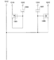
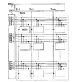
本発明の一は、第1のトランジスタと、第2のトランジスタと、第1のトランジスタに流れる電流に対応したゲートとソース間の電圧が保持される第1の容量素子と、第2のトランジスタのしきい値電圧が保持される第2の容量素子と、第1のトランジスタと第2のトランジスタの間に備えられ、第1の容量素子と第2の容量素子を容量結合するためのスイッチング素子とを有する画素を備えたことを特徴とする表示装置である。 According to one embodiment of the present invention, a first transistor, a second transistor, a first capacitor that holds a voltage between a gate and a source corresponding to a current flowing through the first transistor, a second transistor, A second capacitor element that holds the threshold voltage; a switching element that is provided between the first transistor and the second transistor and that capacitively couples the first capacitor element and the second capacitor element; A display device including a pixel having the above.
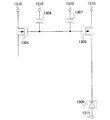
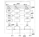
本発明の一は、第1端子が第1の配線に接続され、第2端子が第1のスイッチング素子を介して第2の配線に接続され、第2端子が第2のスイッチング素子を介してゲートに接続される第1のトランジスタと、第1端子が第1の配線に接続され、第2端子が第3のスイッチング素子を介してゲートに接続される第2のトランジスタと、一方の電極が第1の配線に接続され、他方の電極が第1のトランジスタのゲートに接続される第1の容量素子と、一方の電極が第1の配線に接続され、他方の電極が第2のトランジスタのゲートと、第4のスイッチング素子を介して第1の容量素子の他方の電極に接続される第2の容量素子と、一方の電極が、第5のスイッチング素子を介して第1のトランジスタの第2端子に接続される発光素子と、を有する画素を備えたことを特徴とする表示装置である。 In the present invention, the first terminal is connected to the first wiring, the second terminal is connected to the second wiring via the first switching element, and the second terminal is connected to the second switching element. A first transistor connected to the gate; a first terminal connected to the first wiring; a second terminal connected to the gate through the third switching element; and one electrode A first capacitor connected to the first wiring and having the other electrode connected to the gate of the first transistor; one electrode connected to the first wiring; and the other electrode connected to the second transistor A gate, a second capacitor connected to the other electrode of the first capacitor through the fourth switching element, and one electrode connected to the second transistor of the first transistor through the fifth switching element. A light-emitting element connected to two terminals A display device characterized by comprising a pixel.
本発明の一は、第1端子が第1の配線に接続され、第2端子が第1のスイッチング素子を介してゲートに接続される第1のトランジスタと、第1端子が第1の配線に接続され、第2端子が第2のスイッチング素子を介して第2の配線に接続され、第2端子が第3のスイッチング素子を介してゲートに接続される第2のトランジスタと、一方の電極が第1の配線に接続され、他方の電極が第1のトランジスタのゲートに接続される第1の容量素子と、一方の電極が第1の配線に接続され、他方の電極が第2のトランジスタのゲートと、第4のスイッチング素子を介して第1の容量素子の他方の電極に接続される第2の容量素子と、一方の電極が第5のスイッチング素子を介して第1のトランジスタの第2端子に接続される発光素子と、を有する画素を備えたことを特徴とする表示装置である。 According to one aspect of the present invention, the first terminal is connected to the first wiring, the second terminal is connected to the gate through the first switching element, and the first terminal is connected to the first wiring. A second transistor whose second terminal is connected to the second wiring via the second switching element, and whose second terminal is connected to the gate via the third switching element; A first capacitor connected to the first wiring and having the other electrode connected to the gate of the first transistor; one electrode connected to the first wiring; and the other electrode connected to the second transistor A gate, a second capacitor connected to the other electrode of the first capacitor through a fourth switching element, and one electrode of the second transistor of the first transistor via the fifth switching element; A light emitting element connected to the terminal A display device characterized by comprising a prime.
また、第1のトランジスタ及び第2のトランジスタはPチャネル型トランジスタまたはNチャネル型トランジスタであってもよい。 Further, the first transistor and the second transistor may be P-channel transistors or N-channel transistors.
また、第1のトランジスタのチャネル長は、第2のトランジスタのチャネル長より長くすることができる。また、第1のトランジスタのチャネル幅は、第2のトランジスタのチャネル幅より広くすることができる。 In addition, the channel length of the first transistor can be longer than the channel length of the second transistor. In addition, the channel width of the first transistor can be wider than that of the second transistor.
また、第1のトランジスタが発光素子に直列に接続され、第1のトランジスタに流れる電流を制御して、発光素子の発光輝度を制御することができる。 In addition, the first transistor is connected in series to the light-emitting element, and the light emission luminance of the light-emitting element can be controlled by controlling the current flowing through the first transistor.
本発明の一は、第1のトランジスタと、第2のトランジスタと、第1のトランジスタに流す電流に応じたゲートとソース間の電圧が保持される第1の容量素子と、第2のトランジスタのしきい値電圧が保持される第2の容量素子と、第1のトランジスタと第2のトランジスタの間に備えられ、第1の容量素子と第2の容量素子を容量結合するためのスイッチング素子とを備えた画素を有する駆動方法であって、第1のトランジスタのゲートとソース間の電圧が第1の容量素子に保持される動作と、第2のゲートとソース間の電圧が第2の容量素子に保持される動作を同じ期間に行い、その後第1の容量素子と第2の容量素子を、スイッチング素子をオンすることにより容量結合する動作を行うことを特徴とする表示装置の駆動方法である。 According to one embodiment of the present invention, a first capacitor, a second transistor, a first capacitor that holds a voltage between a gate and a source in accordance with a current flowing through the first transistor, and a second transistor A second capacitor element that holds the threshold voltage; a switching element that is provided between the first transistor and the second transistor and that capacitively couples the first capacitor element and the second capacitor element; And a voltage between the gate and the source of the first transistor is held in the first capacitor, and a voltage between the second gate and the source is the second capacitance. An operation of a display device is characterized in that an operation held in an element is performed in the same period, and then an operation of capacitively coupling the first capacitor element and the second capacitor element by turning on a switching element is performed. is there.
本発明の一は、第1端子が第1の配線に接続され、第2端子が第1のスイッチング素子を介して第2の配線に接続され、第2端子が第2のスイッチング素子を介してゲートに接続される第1のトランジスタと、第1端子が第1の配線に接続され、第2端子が第3のスイッチング素子を介してゲートに接続される第2のトランジスタと、一方の電極が第1の配線に接続され、他方の電極が第1のトランジスタのゲートに接続される第1の容量素子と、一方の電極が第1の配線に接続され、他方の電極が第2のトランジスタのゲートと、第4のスイッチング素子を介して第1の容量素子の他方の電極に接続される第2の容量素子と、一方の電極が、第5のスイッチング素子を介して第1のトランジスタの第2端子に接続される発光素子とを有する画素を備えた表示装置の駆動方法であって、第1のトランジスタのゲートとソース間の電圧が第1の容量素子に保持される動作と、第2のトランジスタのゲートとソース間の電圧が第2の容量素子に保持される動作を同じ期間で行い、その後第1の容量素子と第2の容量素子を、第4のスイッチング素子をオンすることにより容量結合する動作を行うことを特徴とする表示装置の駆動方法である。 In the present invention, the first terminal is connected to the first wiring, the second terminal is connected to the second wiring via the first switching element, and the second terminal is connected to the second switching element. A first transistor connected to the gate; a first terminal connected to the first wiring; a second terminal connected to the gate through the third switching element; and one electrode A first capacitor connected to the first wiring and having the other electrode connected to the gate of the first transistor; one electrode connected to the first wiring; and the other electrode connected to the second transistor A gate, a second capacitor connected to the other electrode of the first capacitor through the fourth switching element, and one electrode connected to the second transistor of the first transistor through the fifth switching element. A light emitting element connected to two terminals A driving method of a display device including an element, wherein a voltage between a gate and a source of a first transistor is held in a first capacitor, and a voltage between a gate and a source of a second transistor is The operation held in the second capacitor element is performed in the same period, and then the first capacitor element and the second capacitor element are capacitively coupled by turning on the fourth switching element. It is a drive method of a display apparatus.
本発明の一は、第1端子が第1の配線に接続され、第2端子が第1のスイッチング素子を介してゲートに接続される第1のトランジスタと、第1端子が第1の配線に接続され、第2端子が第2のスイッチング素子を介して第2の配線と、第3のスイッチング素子を介してゲートに接続される第2のトランジスタと、一方の電極が第1の配線に接続され、他方の電極が第1のトランジスタのゲートに接続される第1の容量素子と、一方の電極が第1の配線に接続され、他方の電極が第2のトランジスタのゲートと、第4のスイッチング素子を介して第1の容量素子の他方の電極に接続される第2の容量素子と、一方の電極が、第5のスイッチング素子を介して第1のトランジスタの第2端子に接続される発光素子とを有する画素を備えた表示装置の駆動方法であって、第1のトランジスタのゲートとソースとの間の電圧が第1の容量素子に保持される動作と、第2のゲートとソースとの間の電圧が第2の容量素子に保持される動作を同時に行い、その後第1の容量素子と第2の容量素子を第4のスイッチング素子をオンすることにより容量結合する動作を行うことを特徴とする表示装置の駆動方法である。 According to one aspect of the present invention, the first terminal is connected to the first wiring, the second terminal is connected to the gate through the first switching element, and the first terminal is connected to the first wiring. Connected, second terminal connected to second wiring via second switching element, second transistor connected to gate via third switching element, and one electrode connected to first wiring A first capacitor having the other electrode connected to the gate of the first transistor, one electrode connected to the first wiring, the other electrode connected to the gate of the second transistor, A second capacitor element connected to the other electrode of the first capacitor element via the switching element and one electrode connected to the second terminal of the first transistor via the fifth switching element Display device including a pixel having a light emitting element In which the voltage between the gate and the source of the first transistor is held in the first capacitor, and the voltage between the second gate and the source is the second capacitor. The display device driving method is characterized in that the operation held at the same time is performed simultaneously, and then the first capacitive element and the second capacitive element are capacitively coupled by turning on the fourth switching element. .
なお、本発明に示すスイッチは、様々な形態のものを用いることができ、一例として、電気的スイッチや機械的なスイッチなどがある。つまり、電流の流れを制御できるものであればよく、特定のものに限定されず、様々なものを用いることができる。例えば、トランジスタでもよいし、ダイオード(例えば、PNダイオード、PINダイオード、ショットキーダイオード、ダイオード接続のトランジスタなど)でもよいし、サイリスタでもよいし、それらを組み合わせた論理回路でもよい。よって、スイッチとしてトランジスタを用いる場合、そのトランジスタは、単なるスイッチとして動作するため、トランジスタの極性(導電型)は特に限定されない。ただし、オフ電流が少ない方が望ましい場合、オフ電流が少ない方の極性のトランジスタを用いることが望ましい。オフ電流が少ないトランジスタとしては、LDD領域を設けているものやマルチゲート構造にしているもの等がある。また、スイッチとして動作させるトランジスタのソース端子の電位が、低電位側電源(Vss、GND、0Vなど)に近い状態で動作する場合はNチャネル型を、反対に、ソース端子の電位が、高電位側電源(Vddなど)に近い状態で動作する場合はPチャネル型を用いることが望ましい。なぜなら、ゲートソース間電圧の絶対値を大きくできるため、スイッチとして、動作しやすいからである。 Note that various types of switches can be used as a switch shown in the present invention, and examples thereof include an electrical switch and a mechanical switch. In other words, any device can be used as long as it can control the flow of current, and it is not limited to a specific device, and various devices can be used. For example, it may be a transistor, a diode (for example, a PN diode, a PIN diode, a Schottky diode, a diode-connected transistor, or the like), a thyristor, or a logic circuit that combines them. Therefore, when a transistor is used as a switch, the transistor operates as a mere switch, and thus the polarity (conductivity type) of the transistor is not particularly limited. However, when it is desirable that the off-state current is small, it is desirable to use a transistor having a polarity with a small off-state current. As a transistor with low off-state current, there are a transistor provided with an LDD region and a transistor having a multi-gate structure. Further, when the transistor operated as a switch operates at a source terminal potential close to a low potential power source (Vss, GND, 0 V, etc.), the N-channel type is used. On the contrary, the source terminal potential is a high potential. When operating in a state close to the side power supply (Vdd or the like), it is desirable to use a P-channel type. This is because the absolute value of the voltage between the gate and the source can be increased, so that it can easily operate as a switch.
なお、Nチャネル型とPチャネル型の両方を用いて、CMOS型のスイッチにしてもよい。CMOS型のスイッチにすると、Pチャネル型かNチャネル型かのどちらかのスイッチが導通すれば電流を流すことができるため、スイッチとして機能しやすくなる。例えば、スイッチへの入力信号の電圧が高い場合でも、低い場合でも、適切に電圧を出力させることが出来る。また、スイッチをオン・オフさせるための信号の電圧振幅値を小さくすることが出来るので、消費電力を小さくすることも出来る。 Note that both N-channel and P-channel switches may be used as CMOS switches. When a CMOS switch is used, a current can flow when either the P-channel switch or the N-channel switch is turned on, so that the switch can easily function as a switch. For example, the voltage can be appropriately output regardless of whether the voltage of the input signal to the switch is high or low. In addition, since the voltage amplitude value of the signal for turning on / off the switch can be reduced, the power consumption can be reduced.
なお、スイッチとしてトランジスタを用いる場合は、入力端子(ソース端子またはドレイン端子の一方)と、出力端子(ソース端子またはドレイン端子の他方)と、導通を制御する端子(ゲート端子)とを有している。一方、スイッチとしてダイオードを用いる場合は、導通を制御する端子を有していない場合がある。そのため、端子を制御するための配線を少なくすることが出来る。 Note that in the case where a transistor is used as a switch, the transistor has an input terminal (one of a source terminal or a drain terminal), an output terminal (the other of the source terminal or the drain terminal), and a terminal for controlling conduction (a gate terminal). Yes. On the other hand, when a diode is used as a switch, it may not have a terminal for controlling conduction. Therefore, the wiring for controlling the terminals can be reduced.
なお、本発明において、接続されているとは、電気的に接続されている場合と機能的に接続されている場合と直接接続されている場合とを含むものとする。したがって、本発明が開示する構成において、所定の接続関係以外のものも含むものとする。例えば、ある部分とある部分との間に、電気的な接続を可能とする素子(例えば、スイッチやトランジスタや容量素子やインダクタや抵抗素子やダイオードなど)が1個以上配置されていてもよい。また、機能的な接続を可能とする回路(例えば、論理回路(インバータやNAND回路やNOR回路など)や信号変換回路(DA変換回路やAD変換回路やガンマ補正回路など)や電位レベル変換回路(昇圧回路や降圧回路などの電源回路やH信号やL信号の電位レベルを変えるレベルシフタ回路など)や電圧源や電流源や切り替え回路や増幅回路(オペアンプや差動増幅回路やソースフォロワ回路やバッファ回路など、信号振幅や電流量などを大きく出来る回路など)や信号生成回路や記憶回路や制御回路など)が間に1個以上配置されていてもよい。あるいは、間に他の素子や他の回路を挟まずに、直接接続されて、配置されていてもよい。 Note that in the present invention, the term “connected” includes the case of being electrically connected, the case of being functionally connected, and the case of being directly connected. Therefore, the configuration disclosed by the present invention includes other than the predetermined connection relationship. For example, one or more elements (for example, a switch, a transistor, a capacitor, an inductor, a resistor, a diode, or the like) that can be electrically connected may be arranged between a certain portion. In addition, a circuit (for example, a logic circuit (an inverter, a NAND circuit, a NOR circuit, etc.), a signal conversion circuit (a DA conversion circuit, an AD conversion circuit, a gamma correction circuit, etc.) or a potential level conversion circuit ( Power supply circuits such as booster circuits and step-down circuits, level shifter circuits that change the potential level of H and L signals, etc., voltage sources, current sources, switching circuits, and amplifier circuits (op amps, differential amplifier circuits, source follower circuits, and buffer circuits) Etc.), or a signal generation circuit, a memory circuit, a control circuit, etc.) may be disposed between them. Alternatively, they may be arranged directly connected without interposing other elements or other circuits therebetween.
なお、素子や回路を間に介さずに接続されている場合のみを含む場合は、直接接続されている、と記載するものとする。また、電気的に接続されている、と記載する場合は、電気的に接続されている場合(つまり、間に別の素子を挟んで接続されている場合)と機能的に接続されている場合(つまり、間に別の回路を挟んで接続されている場合)と直接接続されている場合(つまり、間に別の素子や別の回路を挟まずに接続されている場合)とを含むものとする。 In addition, when only including the case where it is connected without interposing an element or a circuit, it shall be described as being directly connected. In addition, when it is described as being electrically connected, when it is electrically connected (that is, when connected with another element in between) and when it is functionally connected (That is, connected with another circuit in between) and directly connected (that is, connected without another element or circuit in between). .
なお、表示素子や表示装置や発光素子や発光装置は、様々な形態を用いたり、様々な素子を有したりすることが出来る。例えば、表示素子や表示装置や発光素子や発光装置としては、EL素子(有機EL素子、無機EL素子又は有機物及び無機物を含むEL素子)、電子放出素子、液晶素子、電子インク、グレーティングライトバルブ(GLV)、プラズマディスプレイ(PDP)、デジタルマイクロミラーデバイス(DMD)、圧電セラミックディスプレイ、カーボンナノチューブ、など、電気磁気的作用によりコントラストが変化する表示媒体を適用することができる。なお、EL素子を用いた表示装置としてはELディスプレイ、電子放出素子を用いた表示装置としてはフィールドエミッションディスプレイ(FED)やSED方式平面型ディスプレイ(SED:Surface−conductionElectron−emitterDisplay)など、液晶素子を用いた表示装置としては液晶ディスプレイ、透過型液晶ディスプレイ、半透過型液晶ディスプレイ、反射型液晶ディスプレイ、電子インクを用いた表示装置としては電子ペーパーがある。 Note that the display element, the display device, the light-emitting element, and the light-emitting device can have various forms or have various elements. For example, as a display element, a display device, a light emitting element, and a light emitting device, an EL element (an organic EL element, an inorganic EL element, or an EL element containing an organic substance and an inorganic substance), an electron emitting element, a liquid crystal element, electronic ink, a grating light valve ( GLV), plasma display (PDP), digital micromirror device (DMD), piezoelectric ceramic display, carbon nanotube, and other display media whose contrast is changed by an electromagnetic action can be applied. Note that an EL display is used as a display device using an EL element, and a liquid crystal device such as a field emission display (FED) or a SED type flat display (SED: Surface-conduction Electron-emitter Display) is used as a display device using an electron-emitting device. Examples of the display device used include a liquid crystal display, a transmissive liquid crystal display, a transflective liquid crystal display, a reflective liquid crystal display, and a display device using electronic ink includes electronic paper.
なお、本発明において、トランジスタは、様々な形態のトランジスタを適用させることが出来る。よって、適用可能なトランジスタの種類に限定はない。したがって、例えば、非晶質シリコンや多結晶シリコンに代表される非単結晶半導体膜を有する薄膜トランジスタ(TFT)などを適用することが出来る。これらにより、製造温度が高くなくても製造できたり、低コストで製造できたり、大型基板上に製造できたり、透明基板上に製造できたり、トランジスタで光を透過させたりすることが出来る。また、半導体基板やSOI基板を用いて形成されるMOS型トランジスタ、接合型トランジスタ、バイポーラトランジスタなどを適用することが出来る。これらにより、バラツキの少ないトランジスタを製造できたり、電流供給能力の高いトランジスタを製造できたり、サイズの小さいトランジスタを製造できたり、消費電力の少ない回路を構成したりすることが出来る。また、ZnO、a−InGaZnO、SiGe、GaAsなどの化合物半導体を有するトランジスタや、さらに、それらを薄膜化した薄膜トランジスタなどを適用することが出来る。これらにより、製造温度が高くなくても製造できたり、室温で製造できたり、耐熱性の低い基板、例えばプラスチック基板やフィルム基板に直接トランジスタを形成したりすることが出来る。 Note that in the present invention, various types of transistors can be used as a transistor. Thus, there is no limitation on the type of applicable transistor. Therefore, for example, a thin film transistor (TFT) including a non-single-crystal semiconductor film typified by amorphous silicon or polycrystalline silicon can be used. As a result, they can be manufactured even at a low manufacturing temperature, can be manufactured at low cost, can be manufactured on a large substrate, can be manufactured on a transparent substrate, and light can be transmitted through a transistor. Alternatively, a MOS transistor, a junction transistor, a bipolar transistor, or the like formed using a semiconductor substrate or an SOI substrate can be used. Accordingly, a transistor with little variation can be manufactured, a transistor with high current supply capability can be manufactured, a transistor with a small size can be manufactured, and a circuit with low power consumption can be configured. In addition, a transistor including a compound semiconductor such as ZnO, a-InGaZnO, SiGe, or GaAs, or a thin film transistor obtained by thinning them can be used. Accordingly, the transistor can be manufactured even at a low manufacturing temperature, can be manufactured at room temperature, or a transistor can be directly formed on a substrate having low heat resistance, such as a plastic substrate or a film substrate.
また、インクジェットや印刷法を用いて作成したトランジスタなどを適用することが出来る。これらにより、室温で製造したり、真空度の低い状態で製造したり、大型基板で製造したりすることができる。また、マスク(レチクル)を用いなくても製造することが可能となるため、トランジスタのレイアウトを容易に変更することが出来る。また、有機半導体やカーボンナノチューブを有するトランジスタ、その他のトランジスタを適用することができる。これらにより、曲げることが可能な基板上にトランジスタを形成することが出来る。 In addition, a transistor formed using an inkjet method or a printing method can be used. By these, it can manufacture at room temperature, can manufacture in a state with a low degree of vacuum, or can manufacture with a large sized board | substrate. Further, since the transistor can be manufactured without using a mask (reticle), the layout of the transistor can be easily changed. In addition, a transistor including an organic semiconductor or a carbon nanotube, or another transistor can be used. Thus, a transistor can be formed over a substrate that can be bent.
なお、非単結晶半導体膜には水素またはハロゲンが含まれていてもよい。また、トランジスタが配置されている基板の種類は、様々なものを用いることができ、特定のものに限定されることはない。従って例えば、単結晶基板、SOI基板、ガラス基板、石英基板、プラスチック基板、紙基板、セロファン基板、石材基板、ステンレス・スチル基板、ステンレス・スチル・ホイルを有する基板などに配置することが出来る。また、ある基板でトランジスタを形成し、その後、別の基板にトランジスタを移動させて、別の基板上に配置するようにしてもよい。これらの基板を用いることにより、特性のよいトランジスタを形成したり、消費電力の小さいトランジスタを形成したり、壊れにくい装置にしたり、耐熱性を持たせたりすることが出来る。 Note that the non-single-crystal semiconductor film may contain hydrogen or halogen. In addition, various types of substrates on which the transistor is arranged can be used, and the substrate is not limited to a specific type. Therefore, for example, it can be disposed on a single crystal substrate, an SOI substrate, a glass substrate, a quartz substrate, a plastic substrate, a paper substrate, a cellophane substrate, a stone substrate, a stainless steel substrate, a stainless steel substrate, a foil substrate, or the like. Alternatively, a transistor may be formed using a certain substrate, and then the transistor may be moved to another substrate and placed on another substrate. By using these substrates, it is possible to form a transistor with good characteristics, to form a transistor with low power consumption, to make the device hard to break, or to have heat resistance.
なお、トランジスタの構成は、様々な形態をとることができる。特定の構成に限定されない。例えば、ゲート電極が2個以上になっているマルチゲート構造を用いてもよい。マルチゲート構造にすると、チャネル領域が直列に接続されるような構成となるため、複数のトランジスタが直列に接続されたような構成となる。マルチゲート構造にすることにより、オフ電流を低減したり、トランジスタの耐圧を向上させて信頼性を良くしたり、飽和領域で動作する時に、ドレイン・ソース間電圧が変化しても、ドレイン・ソース間電流があまり変化せず、フラットな特性にすることなどができる。また、チャネルの上下にゲート電極が配置されている構造でもよい。チャネルの上下にゲート電極が配置されている構造にすることにより、チャネル領域が増えるため、電流値を大きくしたり、空乏層ができやすくなってS値をよくしたりすることができる。チャネルの上下にゲート電極が配置されると、複数のトランジスタが並列に接続されたような構成となる。 Note that the structure of the transistor can take a variety of forms. It is not limited to a specific configuration. For example, a multi-gate structure having two or more gate electrodes may be used. When the multi-gate structure is used, the channel regions are connected in series, so that a plurality of transistors are connected in series. The multi-gate structure reduces the off current, improves the breakdown voltage of the transistor to improve reliability, and even when the drain-source voltage changes when operating in the saturation region. The inter-current does not change so much, and flat characteristics can be achieved. Alternatively, a structure in which gate electrodes are arranged above and below the channel may be employed. By adopting a structure in which gate electrodes are arranged above and below the channel, the channel region increases, so that the current value can be increased, and a depletion layer can be easily formed to improve the S value. When gate electrodes are provided above and below a channel, a structure in which a plurality of transistors are connected in parallel is obtained.
また、チャネルの上にゲート電極が配置されている構造でもよいし、チャネルの下にゲート電極が配置されている構造でもよいし、正スタガ構造であってもよいし、逆スタガ構造でもよいし、チャネル領域が複数の領域に分かれていてもよいし、並列に接続されていてもよいし、直列に接続されていてもよい。また、チャネル(もしくはその一部)にソース電極やドレイン電極が重なっていてもよい。チャネル(もしくはその一部)にソース電極やドレイン電極が重なっている構造にすることにより、チャネルの一部に電荷がたまって、動作が不安定になることを防ぐことができる。また、LDD領域があってもよい。LDD領域を設けることにより、オフ電流を低減したり、トランジスタの耐圧を向上させて信頼性を良くしたり、飽和領域で動作する時に、ドレイン・ソース間電圧が変化しても、ドレイン・ソース間電流があまり変化せず、フラットな特性にすることができる。 Further, a structure in which a gate electrode is disposed above a channel, a structure in which a gate electrode is disposed below a channel, a normal staggered structure, or an inverted staggered structure may be employed. The channel region may be divided into a plurality of regions, may be connected in parallel, or may be connected in series. In addition, a source electrode or a drain electrode may overlap with the channel (or a part thereof). By using a structure in which a source electrode or a drain electrode overlaps with a channel (or part of it), it is possible to prevent electric charges from being accumulated in part of the channel and unstable operation. There may also be an LDD region. By providing an LDD region, the off-current can be reduced, the breakdown voltage of the transistor can be improved to improve reliability, or the drain-source voltage can be changed even when the drain-source voltage changes when operating in the saturation region. The current does not change so much, and a flat characteristic can be obtained.
なお、本発明におけるトランジスタは、様々なタイプを用いることができ、様々な基板上に形成させることができる。したがって、回路の全てが、ガラス基板上に形成されていてもよいし、プラスチック基板に形成されていてもよいし、単結晶基板に形成されていてもよいし、SOI基板上に形成されていてもよいし、どのような基板上に形成されていてもよい。回路の全てが同じ基板上に形成されていることにより、部品点数を減らしてコストを低減したり、回路部品との接続点数を減らして信頼性を向上させたりすることができる。あるいは、回路の一部が、ある基板に形成されており、回路の別の一部が、別の基板に形成されていてもよい。つまり、回路の全てが同じ基板上に形成されていなくてもよい。例えば、回路の一部は、ガラス基板上にトランジスタを用いて形成し、回路の別の一部は、単結晶基板上に形成し、そのICチップをCOG(Chip−On−Glass)で接続してガラス基板上に配置してもよい。あるいは、そのICチップをTAB(Tape−Automatede−Bonding)やプリント基板を用いてガラス基板と接続してもよい。このように、回路の一部が同じ基板に形成されていることにより、部品点数を減らしてコストを低減したり、回路部品との接続点数を減らして信頼性を向上させたりすることができる。また、駆動電圧が高い部分や駆動周波数が高い部分は、消費電力が大きくなってしまうので、そのような部分は同じ基板に形成しないようにすれば、消費電力の向上を防ぐことができる。 Note that various types of transistors can be used in the present invention and can be formed over various substrates. Therefore, the entire circuit may be formed on a glass substrate, may be formed on a plastic substrate, may be formed on a single crystal substrate, or may be formed on an SOI substrate. Alternatively, it may be formed on any substrate. Since all the circuits are formed on the same substrate, the number of parts can be reduced to reduce the cost, and the number of connection points with circuit parts can be reduced to improve the reliability. Alternatively, a part of the circuit may be formed on a certain substrate, and another part of the circuit may be formed on another substrate. That is, all of the circuits may not be formed on the same substrate. For example, part of a circuit is formed using a transistor over a glass substrate, another part of the circuit is formed over a single crystal substrate, and the IC chip is connected by COG (Chip-On-Glass). May be arranged on a glass substrate. Alternatively, the IC chip may be connected to the glass substrate using TAB (Tape-Automated-Bonding) or a printed board. As described above, since a part of the circuit is formed on the same substrate, the number of parts can be reduced to reduce the cost, and the number of connection points with the circuit parts can be reduced to improve the reliability. In addition, since the power consumption increases in a portion where the drive voltage is high or a portion where the drive frequency is high, an improvement in power consumption can be prevented if such a portion is not formed on the same substrate.
なお、本発明においては、一画素とは、明るさを制御できる要素一つ分を示すものとする。よって、一例としては、一画素とは、一つの色要素を示すものとし、その色要素一つで明るさを表現する。従って、そのときは、R(赤)G(緑)B(青)の色要素からなるカラー表示装置の場合には、画像の最小単位は、Rの画素とGの画素とBの画素との三画素から構成されるものとする。 In the present invention, one pixel represents one element whose brightness can be controlled. Therefore, as an example, one pixel represents one color element, and brightness is expressed by one color element. Therefore, at that time, in the case of a color display device composed of R (red), G (green), and B (blue) color elements, the minimum unit of an image is an R pixel, a G pixel, and a B pixel. It is assumed to be composed of three pixels.
なお、色要素は、三色に限定されず、それ以上の数を用いても良いし、RGB以外の色を用いても良い。例えば、白色を加えて、RGBW(Wは白)としてもよい。また、RGBに、例えば、イエロー、シアン、マゼンタ、エメラルドグリーン、朱色などを一色以上追加したものでもよい。また、例えばRGBの中の少なくとも一色について、類似した色を追加してもよい。例えば、R、G、B1、B2としてもよい。B1とB2とは、どちらも青色であるが、少し周波数が異なっている。このような色要素を用いることにより、より実物に近い表示を行うことができたり、消費電力を低減したりすることが出来る。 Note that the color elements are not limited to three colors, and more than that may be used, or colors other than RGB may be used. For example, RGBW (W is white) may be added by adding white. Further, RGB may be obtained by adding one or more colors such as yellow, cyan, magenta, emerald green, vermilion, and the like. Further, for example, a similar color may be added for at least one of RGB. For example, R, G, B1, and B2 may be used. B1 and B2 are both blue, but have slightly different frequencies. By using such a color element, it is possible to perform display closer to the real thing or to reduce power consumption.
また、別の例としては、1つの色要素について、複数の領域を用いて明るさを制御する場合は、その領域一つ分を一画素とする。よって、一例としては、面積階調を行う場合、一つの色要素につき、明るさを制御する領域が複数あり、その全体で階調を表現するわけであるが、明るさを制御する領域の一つ分を一画素とする。よって、その場合は、一つの色要素は、複数の画素で構成されることとなる。また、その場合、画素によって、表示に寄与する領域の大きさが異なっている場合がある。また、一つの色要素につき複数ある、明るさを制御する領域において、つまり、一つの色要素を構成する複数の画素において、各々に供給する信号を僅かに異ならせるようにして、視野角を広げるようにしてもよい。 As another example, in the case where brightness is controlled using a plurality of areas for one color element, one area corresponds to one pixel. Therefore, as an example, when performing area gradation, there are a plurality of areas for controlling the brightness for each color element, and the gradation is expressed as a whole. One portion is defined as one pixel. Therefore, in that case, one color element is composed of a plurality of pixels. In that case, the size of the region contributing to the display may differ depending on the pixel. Further, in a plurality of brightness control areas for one color element, that is, in a plurality of pixels constituting one color element, a signal supplied to each is slightly different to widen the viewing angle. You may do it.
なお、一画素(三色分)と記載する場合は、RとGとBの三画素分を一画素と考える場合であるとする。一画素(一色分)と記載する場合は、一つの色要素につき、複数の画素がある場合、それらをまとめて一画素と考える場合であるとする。 Note that the description of one pixel (for three colors) is a case where three pixels of R, G, and B are considered as one pixel. In the case of describing one pixel (for one color), it is assumed that when there are a plurality of pixels for one color element, they are collectively considered as one pixel.
なお、本発明において、画素は、マトリクス状に配置(配列)されている場合を含んでいる。ここで、画素がマトリクスに配置(配列)されているとは、縦方向もしくは横方向において、直線上に並んで配置されている場合や、ギザギザな線上に並んでいる場合を含んでいる。よって、例えば三色の色要素(例えばRGB)でフルカラー表示を行う場合に、ストライプ配置されている場合や、三つの色要素のドットがいわゆるデルタ配置されている場合も含むものとする。さらに、ベイヤー配置されている場合も含んでいる。なお、色要素は、三色に限定されず、それ以上でもよく、例えば、RGBW(Wは白)や、RGBに、イエロー、シアン、マゼンタなどを一色以上追加したものなどがある。また、色要素のドット毎にその表示領域の大きさが異なっていてもよい。これにより、消費電力を低下させたり、表示素子の寿命を延ばしたりすることが出来る。 In the present invention, the case where the pixels are arranged (arranged) in a matrix is included. Here, the arrangement (arrangement) of pixels in a matrix includes a case where pixels are arranged side by side in a vertical direction or a horizontal direction or a case where they are arranged on a jagged line. Therefore, for example, when full color display is performed with three color elements (for example, RGB), the case where stripes are arranged and the case where dots of three color elements are arranged in a so-called delta are also included. Furthermore, the case where a Bayer is arranged is also included. Note that the color elements are not limited to three colors, and may be more than that, for example, RGBW (W is white) or RGB in which one or more colors of yellow, cyan, magenta, and the like are added. Further, the size of the display area may be different for each dot of the color element. Thereby, power consumption can be reduced and the lifetime of the display element can be extended.
なお、トランジスタとは、それぞれ、ゲートと、ドレインと、ソースとを含む少なくとも三つの端子を有する素子であり、ドレイン領域とソース領域の間にチャネル領域を有しており、ドレイン領域とチャネル領域とソース領域とを介して電流を流すことが出来る。ここで、ソースとドレインとは、トランジスタの構造や動作条件等によって変わるため、いずれがソースまたはドレインであるかを限定することが困難である。そこで、本発明においては、ソース及びドレインとして機能する領域を、ソースもしくはドレインと呼ばない場合がある。その場合、一例としては、それぞれを第1端子、第2端子と表記する場合がある。 Note that a transistor is an element having at least three terminals including a gate, a drain, and a source, and has a channel region between the drain region and the source region. Current can flow through the source region. Here, since the source and the drain vary depending on the structure and operating conditions of the transistor, it is difficult to limit which is the source or the drain. Therefore, in the present invention, a region functioning as a source and a drain may not be called a source or a drain. In that case, as an example, there are cases where they are referred to as a first terminal and a second terminal, respectively.
なお、トランジスタは、ベースとエミッタとコレクタとを含む少なくとも三つの端子を有する素子であってもよい。この場合も同様に、エミッタとコレクタとを、第1端子、第2端子と表記する場合がある。 Note that the transistor may be an element having at least three terminals including a base, an emitter, and a collector. Similarly in this case, the emitter and the collector may be referred to as a first terminal and a second terminal.
なお、ゲートとは、ゲート電極とゲート配線(ゲート線またはゲート信号線等とも言う)とを含んだ全体、もしくは、それらの一部のことを言う。ゲート電極とは、チャネル領域やLDD(Lightly−Doped−Drain)領域などを形成する半導体と、ゲート絶縁膜を介してオーバーラップしている部分の導電膜のことを言う。ゲート配線とは、各画素のゲート電極の間を接続したり、ゲート電極と別の配線とを接続したりするための配線のことを言う。 Note that a gate refers to the whole or part of a gate electrode and a gate wiring (also referred to as a gate line or a gate signal line). A gate electrode refers to a portion of a conductive film that overlaps with a semiconductor that forms a channel region, an LDD (Lightly-Doped-Drain) region, and the like with a gate insulating film interposed therebetween. The gate wiring refers to wiring for connecting between the gate electrodes of each pixel or connecting the gate electrode to another wiring.
ただし、ゲート電極としても機能し、ゲート配線としても機能するような部分も存在する。そのような領域は、ゲート電極と呼んでも良いし、ゲート配線と呼んでも良い。つまり、ゲート電極とゲート配線とが、明確に区別できないような領域も存在する。例えば、延伸して配置されているゲート配線とオーバーラップしてチャネル領域がある場合、その領域はゲート配線として機能しているが、ゲート電極としても機能していることになる。よって、そのような領域は、ゲート電極と呼んでも良いし、ゲート配線と呼んでも良い。 However, there is a portion that functions as a gate electrode and also functions as a gate wiring. Such a region may be called a gate electrode or a gate wiring. That is, there is a region where the gate electrode and the gate wiring cannot be clearly distinguished. For example, when there is a channel region that overlaps with an extended gate wiring, the region functions as a gate wiring, but also functions as a gate electrode. Therefore, such a region may be called a gate electrode or a gate wiring.
また、ゲート電極と同じ材料で形成され、ゲート電極とつながっている領域も、ゲート電極と呼んでも良い。同様に、ゲート配線と同じ材料で形成され、ゲート配線とつながっている領域も、ゲート配線と呼んでも良い。このような領域は、厳密な意味では、チャネル領域とオーバーラップしていなかったり、別のゲート電極と接続させる機能を有してなかったりする場合がある。しかし、製造マージンなどの関係で、ゲート電極やゲート配線と同じ材料で形成され、ゲート電極やゲート配線とつながっている領域がある。よって、そのような領域もゲート電極やゲート配線と呼んでも良い。 A region formed of the same material as the gate electrode and connected to the gate electrode may also be called a gate electrode. Similarly, a region formed of the same material as the gate wiring and connected to the gate wiring may be called a gate wiring. In a strict sense, such a region may not overlap with the channel region or may not have a function of being connected to another gate electrode. However, there is a region that is formed of the same material as the gate electrode and the gate wiring and connected to the gate electrode and the gate wiring because of a manufacturing margin. Therefore, such a region may also be called a gate electrode or a gate wiring.
また、例えば、マルチゲートのトランジスタにおいて、1つのトランジスタのゲート電極と、別のトランジスタのゲート電極とは、ゲート電極と同じ材料で形成された導電膜で接続される場合が多い。そのような領域は、ゲート電極とゲート電極とを接続させるための領域であるため、ゲート配線と呼んでも良いが、マルチゲートのトランジスタを1つのトランジスタであると見なすことも出来るため、ゲート電極と呼んでも良い。つまり、ゲート電極やゲート配線と同じ材料で形成され、それらとつながって配置されているものは、ゲート電極やゲート配線と呼んでも良い。 For example, in a multi-gate transistor, the gate electrode of one transistor and the gate electrode of another transistor are often connected by a conductive film formed using the same material as the gate electrode. Such a region is a region for connecting the gate electrode and the gate electrode, and may be referred to as a gate wiring. However, a multi-gate transistor can be regarded as one transistor, You can call it. That is, what is formed of the same material as the gate electrode and the gate wiring and is connected to the gate electrode and the gate wiring may be called a gate electrode and a gate wiring.
また、例えば、ゲート電極とゲート配線とを接続してさせている部分の導電膜も、ゲート電極と呼んでも良いし、ゲート配線と呼んでも良い。 Further, for example, a conductive film in a portion where the gate electrode and the gate wiring are connected to each other may be referred to as a gate electrode or a gate wiring.
なお、ゲート端子とは、ゲート電極の領域や、ゲート電極と電気的に接続されている領域について、その一部分のことを言う。 Note that a gate terminal refers to a part of a region of a gate electrode or a region electrically connected to the gate electrode.
なお、ソースとは、ソース領域とソース電極とソース配線(ソース線またはソース信号線等とも言う)とを含んだ全体、もしくは、それらの一部のことを言う。ソース領域とは、P型不純物(ボロンやガリウムなど)やN型不純物(リンやヒ素など)が多く含まれる半導体領域のことを言う。従って、少しだけP型不純物やN型不純物が含まれる領域、いわゆる、LDD(Lightly−Doped−Drain)領域は、ソース領域には含まれない。ソース電極とは、ソース領域とは別の材料で形成され、ソース領域と電気的に接続されて配置されている部分の導電層のことを言う。ただし、ソース電極は、ソース領域も含んでソース電極と呼ぶこともある。ソース配線とは、各画素のソース電極の間を接続したり、ソース電極と別の配線とを接続したりするための配線のことを言う。 Note that a source refers to the whole or part of a source region, a source electrode, and a source wiring (also referred to as a source line, a source signal line, or the like). The source region refers to a semiconductor region containing a large amount of P-type impurities (such as boron and gallium) and N-type impurities (such as phosphorus and arsenic). Therefore, a region containing a little P-type impurity or N-type impurity, that is, a so-called LDD (Lightly-Doped-Drain) region is not included in the source region. A source electrode refers to a portion of a conductive layer which is formed using a material different from that of a source region and is electrically connected to the source region. However, the source electrode may be referred to as a source electrode including the source region. The source wiring is a wiring for connecting between the source electrodes of each pixel or connecting the source electrode and another wiring.
しかしながら、ソース電極としても機能し、ソース配線としても機能するような部分も存在する。そのような領域は、ソース電極と呼んでも良いし、ソース配線と呼んでも良い。つまり、ソース電極とソース配線とが、明確に区別できないような領域も存在する。例えば、延伸して配置されているソース配線とオーバーラップしてソース領域がある場合、その領域はソース配線として機能しているが、ソース電極としても機能していることになる。よって、そのような領域は、ソース電極と呼んでも良いし、ソース配線と呼んでも良い。 However, there is a portion that functions as a source electrode and also functions as a source wiring. Such a region may be called a source electrode or a source wiring. That is, there is a region where the source electrode and the source wiring cannot be clearly distinguished. For example, when there is a source region that overlaps with an extended source wiring, the region functions as a source wiring, but also functions as a source electrode. Therefore, such a region may be called a source electrode or a source wiring.
また、ソース電極と同じ材料で形成され、ソース電極とつながっている領域や、ソース電極とソース電極とを接続される部分も、ソース電極と呼んでも良い。また、ソース領域とオーバーラップしている部分も、ソース電極と呼んでも良い。同様に、ソース配線と同じ材料で形成され、ソース配線とつながっている領域も、ソース配線と呼んでも良い。このような領域は、厳密な意味では、別のソース電極と接続させる機能を有していたりすることがない場合がある。しかし、製造マージンなどの関係で、ソース電極やソース配線と同じ材料で形成され、ソース電極やソース配線とつながっている領域がある。よって、そのような領域もソース電極やソース配線と呼んでも良い。 In addition, a region formed of the same material as the source electrode and connected to the source electrode, or a portion where the source electrode and the source electrode are connected may be called a source electrode. A portion overlapping with the source region may also be called a source electrode. Similarly, a region formed of the same material as the source wiring and connected to the source wiring may be called a source wiring. In a strict sense, such a region may not have a function of connecting to another source electrode. However, there is a region formed of the same material as the source electrode and the source wiring and connected to the source electrode and the source wiring because of a manufacturing margin. Therefore, such a region may also be called a source electrode or a source wiring.
また、例えば、ソース電極とソース配線とを接続してさせている部分の導電膜も、ソース電極と呼んでも良いし、ソース配線と呼んでも良い。 In addition, for example, a conductive film in a portion where the source electrode and the source wiring are connected to each other may be referred to as a source electrode or a source wiring.
なお、ソース端子とは、ソース領域の領域や、ソース電極や、ソース電極と電気的に接続されている領域について、その一部分のことを言う。 Note that a source terminal refers to a part of a source region, a source electrode, or a region electrically connected to the source electrode.
なお、ドレインについては、ソースと同様である。 The drain is the same as the source.
なお、本発明において、半導体装置とは半導体素子(トランジスタやダイオードなど)を含む回路を有する装置をいう。また、半導体特性を利用することで機能しうる装置全般でもよい。 Note that in the present invention, a semiconductor device refers to a device having a circuit including a semiconductor element (such as a transistor or a diode). In addition, any device that can function by utilizing semiconductor characteristics may be used.
また、表示装置とは、表示素子(液晶素子や発光素子など)を有する装置のことを言う。 A display device refers to a device having a display element (such as a liquid crystal element or a light-emitting element).
なお、液晶素子やEL素子などの表示素子を含む複数の画素やそれらの画素を駆動させる周辺駆動回路が同一基板上に形成された表示パネル本体のことでもよい。また、ワイヤボンディングやバンプなどによって基板上に配置された周辺駆動回路、いわゆるチップオングラス(COG)を含んでいても良い。さらに、フレキシブルプリントサーキット(FPC)やプリント配線基盤(PWB)が取り付けられたもの(ICや抵抗素子や容量素子やインダクタやトランジスタなど)も含んでもよい。さらに、偏光板や位相差板などの光学シートを含んでいても良い。さらに、バックライトユニット(導光板やプリズムシートや拡散シートや反射シートや光源(LEDや冷陰極管など)を含んでいても良い)を含んでいても良い。 Note that a display panel body in which a plurality of pixels including display elements such as a liquid crystal element and an EL element and peripheral drive circuits for driving these pixels are formed over the same substrate may be used. Further, it may include a peripheral drive circuit, so-called chip on glass (COG), which is disposed on the substrate by wire bonding or bumps. Furthermore, a device to which a flexible printed circuit (FPC) or a printed wiring board (PWB) is attached (such as an IC, a resistor, a capacitor, an inductor, or a transistor) may also be included. Furthermore, an optical sheet such as a polarizing plate or a retardation plate may be included. Furthermore, a backlight unit (which may include a light guide plate, a prism sheet, a diffusion sheet, a reflection sheet, and a light source (such as an LED or a cold cathode tube)) may be included.
また、発光装置とは、特にEL素子やFEDで用いる素子などの自発光型の表示素子を有している表示装置をいう。液晶表示装置とは、液晶素子を有している表示装置をいう。 A light-emitting device refers to a display device including a self-luminous display element such as an EL element or an element used in an FED. A liquid crystal display device refers to a display device having a liquid crystal element.
なお、本発明において、ある物の上に形成されている、あるいは、〜上に形成されている、というように、〜の上に、あるいは、〜上に、という記載については、ある物の上に直接接していることに限定されない。直接接してはいない場合、つまり、間に別のものが挟まっている場合も含むものとする。従って例えば、層Aの上に(もしくは層A上に)、層Bが形成されている、という場合は、層Aの上に直接接して層Bが形成されている場合と、層Aの上に直接接して別の層(例えば層Cや層Dなど)が形成されていて、その上に直接接して層Bが形成されている場合とを含むものとする。また、〜の上方に、という記載についても同様であり、ある物の上に直接接していることに限定されず、間に別のものが挟まっている場合も含むものとする。従って例えば、層Aの上方に、層Bが形成されている、という場合は、層Aの上に直接接して層Bが形成されている場合と、層Aの上に直接接して別の層(例えば層Cや層Dなど)が形成されていて、その上に直接接して層Bが形成されている場合とを含むものとする。なお、〜の下に、あるいは、〜の下方に、の場合についても、同様であり、直接接している場合と、接していない場合とを含むこととする。 In addition, in the present invention, it is formed on a certain object, or is formed on the top. It is not limited to being in direct contact with. This includes cases where they are not in direct contact, that is, cases where another object is sandwiched between them. Therefore, for example, when the layer B is formed on the layer A (or on the layer A), the case where the layer B is formed in direct contact with the layer A and the case where the layer B is formed In which another layer (for example, layer C or layer D) is formed in direct contact with layer B and layer B is formed in direct contact therewith. The same applies to the description of “above”, and it is not limited to being in direct contact with a certain object, and includes a case where another object is sandwiched therebetween. Therefore, for example, when the layer B is formed above the layer A, the case where the layer B is formed in direct contact with the layer A and the case where another layer is formed in direct contact with the layer A. (For example, the layer C or the layer D) is formed, and the layer B is formed in direct contact therewith. It should be noted that the same applies to the case of below or below, and includes the case of direct contact and the case of no contact.
本発明によれば、ビデオ信号の書き込み期間において、駆動トランジスタのしきい値電圧の取得とビデオ信号の書き込みを同時に行うことによって、書き込み時間を短くすることができる。こうすることで、一画素当たりの書き込み期間を長く有することができ、より確実にビデオ信号を書き込むことができ、より高画質な有機ELディスプレイを提供することができる。また同じ書き込み期間であればより多くの画素に書き込みを行うことができるため、大型のELディスプレイを提供することが可能であり、より解像度の高いELディスプレイを提供することができる。 According to the present invention, the writing time can be shortened by simultaneously obtaining the threshold voltage of the driving transistor and writing the video signal in the writing period of the video signal. By doing so, the writing period per pixel can be long, the video signal can be written more reliably, and an organic EL display with higher image quality can be provided. In addition, since writing can be performed on more pixels in the same writing period, a large EL display can be provided and an EL display with higher resolution can be provided.
本発明の実施形態について、図面を用いて詳細に説明する。但し、本発明は以下の説明に限定されず、本発明の趣旨及びその範囲から逸脱することなくその形態及び詳細をさまざまに変更し得ることは当業者であれば容易に理解される。従って、本発明は以下に示す実施形態の記載内容に限定して解釈されるものではない。 Embodiments of the present invention will be described in detail with reference to the drawings. However, the present invention is not limited to the following description, and it will be easily understood by those skilled in the art that modes and details can be variously changed without departing from the spirit and scope of the present invention. Therefore, the present invention should not be construed as being limited to the description of the embodiments below.
(第1の実施形態)
本実施の形態は、一画素あたりの書き込み時間を短くするために、ビデオ信号を書き込み、EL素子に流す電流を制御するためのトランジスタと、しきい値電圧を取得するためのトランジスタとを設けた表示装置の構成について、図1を参照して説明する。
(First embodiment)
In this embodiment, in order to shorten the writing time per pixel, a transistor for writing a video signal and controlling a current flowing to the EL element and a transistor for acquiring a threshold voltage are provided. The structure of the display device will be described with reference to FIG.
図1において、第1のトランジスタ100は飽和領域で動作するトランジスタであり、ゲートとソースとの間の電圧によってEL素子109に流れる電流値を制御する駆動トランジスタである。第2のトランジスタ101は第1のトランジスタ100としきい値電圧や移動度などの特性が近似しており、第1のトランジスタ100と対をなすトランジスタである。第1のスイッチ102、第2のスイッチ103、第3のスイッチ104、第4のスイッチ105、及び第5のスイッチ106は二つの端子、及び制御端子を有しており、二つの端子の導通(オン)、非導通(オフ)を制御端子によって制御するスイッチング素子である。第1の容量素子107は一対の電極を有しており、第1のトランジスタ100のゲートとソースとの間の電圧を保持するための容量素子である。第2の容量素子108は一対の電極を有しており、第2のトランジスタ101のゲートとソースとの間の電圧を保持するための容量素子である。EL素子109は一対の電極を有しており、電流値に比例して発光輝度が決まるEL素子である。電源線110は1行共通、又は1列共通となっており、画素に電圧を供給するための電源線である。対向電極111は全画素共通となっており、画素に電圧を供給するための対向電極であり、EL素子109の他方電極である。ソース信号線112は1行共通、又は1列共通となっており、画素へのビデオ信号として電流信号を伝達するための信号線である。
In FIG. 1, a
図1の接続関係を説明する。電源線110は第1のトランジスタ100の第1端子、第2のトランジスタ101の第1端子、第1の容量素子107の一方の電極、及び第2の容量素子108の一方の電極と接続されている。第1の容量素子107の他方の電極は第1のトランジスタ100のゲートと接続され、第2の容量素子108の他方の電極は第2のトランジスタ101のゲートと接続されている。第1の容量素子107の他方の電極、及び第1のトランジスタ100のゲートは第4のスイッチ105を介して第2の容量素子108の他方の電極、及び第2のトランジスタ101のゲート接続されている。第1のトランジスタ100の第2端子は第2のスイッチ103を介して第1のトランジスタ100のゲート、第1のスイッチ102を介してソース信号線112、及び第5のスイッチ106を介してEL素子109の一方の電極と接続されている。第2のトランジスタ101の第2端子は第3のスイッチ104を介して第2のトランジスタ101のゲートに接続されている。
The connection relationship in FIG. 1 will be described. The
ここで、第1の容量素子107の一方の電極、及び第2の容量素子108の一方の電極は、動作時に一定となる端子に接続されていればよく、例えば、別の1行前の第1のスイッチ102の制御端子や新たに別の基準線を加えて接続してもよい。第1のスイッチ102、第2のスイッチ103、第3のスイッチ104、第4のスイッチ105、及び第5のスイッチ106の配置に関しては、後に図2で説明する期間T1で図3に示す回路図、期間T2で図4に示す回路図と等価回路にできれば、どこでもよいし、スイッチの数を増やしてもよい。また、図3は期間T1のときの図1の画素回路の等価回路であり、図4は期間T2のときの図1の画素回路の等価回路である。
Here, one electrode of the
図1の動作について、図2のタイミングチャートを参照して説明する。期間T1の動作について説明する。期間T1では、第2のスイッチ103はオンして第1のトランジスタ100がダイオード接続され、第3のスイッチ104がオンして第2のトランジスタ101がダイオード接続される。第4のスイッチ105はオフして第1のトランジスタ100と第2のトランジスタ101は電気的に遮断される。第5のスイッチ106はオフしてEL素子109への電流は遮断される。第1のスイッチ102はオンしてソース信号線112からの電流で入力されるビデオ信号が第1のトランジスタ100に流れ、第1の容量素子107には第1のトランジスタ100に流れる電流がビデオ信号の電流となるようなゲートとソースとの間の電圧を保持する。第2の容量素子108には第2のトランジスタ101に流れる電流がゼロとなるようなゲートとソースとの間の電圧を保持する。つまり、第2のトランジスタ101のしきい値電圧が保持され、第1のトランジスタ100のしきい値などの特性と第2のトランジスタ101の特性(しきい値電圧、移動度など)は近似していることから、第1のトランジスタ100のしきい値電圧とほぼ等しい電圧が保持される。このとき、ビデオ信号として入力するIdataを数式(1)、第1の容量素子107に保持される電圧を数式(2)に示す。
The operation of FIG. 1 will be described with reference to the timing chart of FIG. An operation in the period T1 is described. In the period T1, the
![]()
![]()
![]()
![]()
上記数式(1)、及び数式(2)において、Idataは期間T1において画素に入力されるソース信号線112に流れるビデオ信号の電流値である。βは第1のトランジスタ100のチャネル長、チャネル幅、移動度、酸化膜の容量値などを含む定数である。Vgs(T1)は第1のトランジスタ100のゲートとソースとの間の電圧である。Vthは第1のトランジスタ100と第2のトランジスタ101は対となるトランジスタであるため、第1のトランジスタ100のしきい値電圧であり、第2のトランジスタ101のしきい値電圧でもある。
In the above formulas (1) and (2), Idata is the current value of the video signal flowing in the
期間T2の動作について説明する。期間T2では、第2のスイッチ103はオフして第1のトランジスタ100はダイオード接続ではなくなり、第3のスイッチ104はオフして第2のトランジスタ101はダイオード接続ではなくなる。第4のスイッチ105はオンして第1の容量素子107と第2の容量素子108が接続され、それぞれの容量素子に保持している電圧は容量結合によって分圧される。第5のスイッチ106はオンして第1のトランジスタ100のゲートとソースとの間の電圧に従った電流がEL素子109に流れる。第1のスイッチ102はオフして第1のソース信号線112からのビデオ信号は遮断される。このとき、第1のトランジスタ100のゲート電圧を数式(3)、EL素子109に流れる電流値を数式(4)に示す。
An operation in the period T2 is described. In the period T2, the
![]()
![]()

上記数式(3)、及び数式(4)において、Idata、β、Vth、及びVgs(T1)は期間T1と同様なものとする。Ioledは期間T2においてEL素子109に流れる電流値である。すなわち、IoledはT2期間において第1のトランジスタ100のゲートとソースの間に電圧が保持されたことにより、第1のトランジスタ100に流れる電流に等しい。C107は第1の容量素子107の容量値であり第1のトランジスタ100のゲート容量も含んでおり、C108は第2の容量素子108の容量値であり第2のトランジスタ101のゲート容量も含んでいる。
In the above formulas (3) and (4), Idata, β, Vth, and Vgs (T1) are the same as those in the period T1. Ioled is a current value flowing through the
上記の数式(4)より、Idataを[C107/(C107+C108)]の2乗倍した電流をEL素子109に流すことができる。また、期間T2において、同一のビデオ信号であれば第1のトランジスタ100の特性(しきい値電圧、移動度など)、及び第2のトランジスタ101の特性(しきい値電圧、移動度など)が近似していれば、他の画素との特性がばらついていてもEL素子109に流れる電流値はばらつかない。
From the above formula (4), a current obtained by multiplying Idata to the square of [C107 / (C107 + C108)] can be passed through the
こうして、駆動トランジスタの特性のばらつきを補償し、且つ画素へ入力したビデオ信号の電流よりも小さい電流をEL素子に流すことができる。そのため低階調を表現する場合においても、ビデオ信号として微小な電流を入力せずに、ある程度大きい電流を入力することができるので、ソース信号線の寄生容量などの充電時間を速くすることができる。また、期間T1において、しきい値電圧の取得とビデオ信号の書込みを同時に行うことから一画素あたりの書込み時間を短縮できる。 In this manner, variation in characteristics of the driving transistor can be compensated and a current smaller than the current of the video signal input to the pixel can be supplied to the EL element. Therefore, even when a low gradation is expressed, since a certain amount of current can be input without inputting a minute current as a video signal, charging time such as parasitic capacitance of the source signal line can be increased. . In addition, since the threshold voltage is acquired and the video signal is written simultaneously in the period T1, the writing time per pixel can be shortened.
本実施形態では、第2のスイッチ103と第3のスイッチ104のオン、又はオフのタイミングが同じため制御端子を共通にすることができる。制御端子を共通化することで画素へ入力する信号数、及び配線数を減らすことができるため画素を制御するドライバ回路を簡略化でき、高開口率を実現することができる。
In the present embodiment, since the
第1のトランジスタ100のチャネル幅、チャネル長などは第2のトランジスタ101よりも大きいほうが望ましい。第1のトランジスタ100と第2のトランジスタ101は特性(しきい値電圧、移動度など)が近似していればよく、第1のトランジスタ100は、第2のトランジスタ101よりもチャネル幅を広く、チャネル長を長くすることにより、高開口率を実現することができる。
The channel width, channel length, and the like of the
本実施形態で説明したスイッチング素子の種類について説明する。本発明においてスイッチング素子としては、電流の流れを制御できる素子であれば、電気的スイッチでも機械的スイッチでも良い。スイッチング素子として、ダイオードを用いても良いし、ダイオードとトランジスタを組み合わせた論理回路を用いてもよい。 The kind of switching element demonstrated by this embodiment is demonstrated. In the present invention, the switching element may be an electrical switch or a mechanical switch as long as it can control the flow of current. As the switching element, a diode may be used, or a logic circuit combining a diode and a transistor may be used.
また、本発明において、スイッチング素子として適用可能なトランジスタの種類に限定はなく、非晶質シリコンや多結晶シリコンに代表される非単結晶半導体膜を用いたトランジスタ、半導体基板やSOI基板を用いて形成されるMOS型トランジスタ、接合型トランジスタ、バイポーラトランジスタ、有機半導体やカーボンナノチューブを用いたトランジスタ、その他のトランジスタを適用することができる。また、トランジスタが形成される基板の種類に限定はなく、単結晶基板、SOI基板、石英基板、ガラス基板、樹脂基板などを自由に用いることができる。 In the present invention, the type of transistor that can be used as a switching element is not limited. A transistor using a non-single-crystal semiconductor film typified by amorphous silicon or polycrystalline silicon, a semiconductor substrate, or an SOI substrate is used. A MOS transistor, a junction transistor, a bipolar transistor, a transistor using an organic semiconductor or a carbon nanotube, and other transistors can be applied. There is no limitation on the type of the substrate over which the transistor is formed, and a single crystal substrate, an SOI substrate, a quartz substrate, a glass substrate, a resin substrate, or the like can be used freely.
トランジスタは単なるスイッチング素子として動作させるため、極性(導電型)は特に限定されず、N型トランジスタでもP型トランジスタでもどちらでもよい。ただし、オフ電流が少ない方が望ましい場合、オフ電流が少ない特性のトランジスタを用いることが望ましい。オフ電流が少ないトランジスタとしては、チャネル形成領域とソース領域またはドレイン領域との間に低濃度で導電型を付与する不純物元素が添加された領域(LDD領域という。)が設けられたトランジスタがある。 Since the transistor operates as a mere switching element, the polarity (conductivity type) is not particularly limited and may be either an N-type transistor or a P-type transistor. However, in the case where it is desirable that the off-state current is small, it is desirable to use a transistor having characteristics with a small off-state current. As a transistor with low off-state current, there is a transistor in which a region to which an impurity element imparting a conductivity type is added at a low concentration (referred to as an LDD region) is provided between a channel formation region and a source or drain region.
また、トランジスタのソースの電位が低電位側電源に近い状態で動作する場合には、当該トランジスタはN型とするのが望ましい。反対に、トランジスタのソースの電位が高電位側電源に近い状態で動作する場合には、当該トランジスタはP型とするのが望ましい。このような構成とすることによって、トランジスタのゲートとソース間の電圧の絶対値を大きくできるので、当該トランジスタをスイッチとして動作させやすい。なお、N型トランジスタとP型トランジスタとの両方を用いて、CMOS型のスイッチング素子としてもよい。 In the case where the transistor operates in a state in which the potential of the source of the transistor is close to a low-potential-side power supply, the transistor is preferably N-type. On the other hand, when the transistor operates in a state where the source potential is close to the high-potential side power supply, the transistor is preferably P-type. With such a structure, the absolute value of the voltage between the gate and the source of the transistor can be increased, so that the transistor can be easily operated as a switch. Note that a CMOS switching element may be formed using both an N-type transistor and a P-type transistor.
(第2の実施形態)
第1の実施形態において、スイッチング素子として、トランジスタを用いることができる。本実施の形態は、スイッチング素子として、Pチャネル型トランジスタを用いた場合の構成について、図5を参照して説明する。
(Second Embodiment)
In the first embodiment, a transistor can be used as the switching element. In this embodiment, a structure in the case where a P-channel transistor is used as a switching element will be described with reference to FIG.
図5において、第1のトランジスタ100、第2のトランジスタ101、第1の容量素子107、第2の容量素子108、EL素子109、電源線110、対向電極111、及びソース信号線112は第1の実施形態と同様なものとする。第3のトランジスタ502、第4のトランジスタ503、第5のトランジスタ504、第6のトランジスタ505、及び第7のトランジスタ506はスイッチング素子としての機能を有しており線形領域で動作する。第3のトランジスタ502は第1のゲート信号線512、第4のトランジスタ503は第2のゲート信号線513、第5のトランジスタ504は第3のゲート信号線514、第6のトランジスタ505は第4のゲート信号線515、第7のトランジスタ506は第5のゲート信号線516からのデジタル信号で制御され、Highのときにオフ、Lowのときにオンする。入力されるトランジスタのゲートとソースとの間の電圧がしきい値電圧よりも高くなる信号電圧をHighといい、しきい値電圧よりも低くなる信号電圧をLowという。
In FIG. 5, the
図5の接続関係を説明する。電源線110は第1のトランジスタ100の第1端子、第2のトランジスタ101の第1端子、第1の容量素子107の一方の電極、及び第2の容量素子108の一方の電極と接続されている。第1の容量素子107の他方の電極は第1のトランジスタ100のゲートと接続され、第2の容量素子108の他方の電極は第2のトランジスタ101のゲートと接続されている。第1の容量素子107の他方の電極、及び第1のトランジスタ100のゲートは第6のトランジスタ505の第1端子と接続され、第2の容量素子108の他方の電極、及び第2のトランジスタ101のゲートは第6のトランジスタ505の第2端子と接続されている。第1のトランジスタ100の第2端子は第4のトランジスタ503の第1端子と接続され、第4のトランジスタ503の第2端子は第1のトランジスタ100のゲートと接続されている。第1のトランジスタ100の第2端子は第3のトランジスタ502の第1端子と接続され、第3のトランジスタ502の第2端子はソース信号線112と接続されている。第1のトランジスタ100の第2端子は第7のトランジスタ506の第1端子と接続され、第7のトランジスタ506の第2端子はEL素子109の一方の電極と接続されている。第2のトランジスタ101の第2端子は第5のトランジスタ504の第1端子と接続され、第5のトランジスタ504の第2端子は第2のトランジスタ101のゲートと接続されている。
The connection relationship in FIG. 5 will be described. The
ここで、第1の実施形態と同様に、第1の容量素子107の一方の電極、及び第2の容量素子108の一方の電極は、動作時に一定となる端子に接続されていればよく、例えば、別の1行前の第1のゲート信号線512や新たに別の基準線を加えて接続してもよい。第3のトランジスタ502、第4のトランジスタ503、第5のトランジスタ504、第6のトランジスタ505、及び第7のトランジスタ506の配置に関しては、後に図6で説明する期間T1で図3に示す回路図、期間T2で図4に示す回路図と等価回路にできれば、どこでもよいし、トランジスタの数を増やしてもよい。また、図3は期間T1のときの図5の画素回路の等価回路であり、図4は期間T2のときの図5の画素回路の等価回路である。
Here, as in the first embodiment, one electrode of the
図5の動作について、図6のタイミングチャートを参照して説明する。期間T1の動作について説明する。期間T1では、第4のトランジスタ503はオンして第1のトランジスタ100がダイオード接続され、第5のトランジスタ504がオンして第2のトランジスタ101がダイオード接続される。第6のトランジスタ505はオフして第1のトランジスタ100と第2のトランジスタ101は電気的に遮断される。第7のトランジスタ506はオフしてEL素子109への電流は遮断される。第3のトランジスタ502はオンしてソース信号線112からの電流で入力されるビデオ信号が第1のトランジスタ100に流れ、第1の容量素子107には第1のトランジスタ100に流れる電流がビデオ信号の電流となるようなゲートとソースとの間の電圧を保持される。第2の容量素子108には第2のトランジスタ101に流れる電流がゼロとなるようなゲートとソースとの間の電圧が保持される。つまり、第2のトランジスタ101のしきい値電圧が保持され、第1のトランジスタ100の特性(しきい値電圧、移動度など)と第2のトランジスタ101の特性(しきい値電圧、移動度など)は近似していることから、第1のトランジスタ100のしきい値電圧とほぼ等しい電圧が保持される。このとき、第1の実施形態と同様に、ビデオ信号として入力するIdataは数式(1)、第1の容量素子107に保持される電圧は数式(2)で表すことができる。
The operation of FIG. 5 will be described with reference to the timing chart of FIG. An operation in the period T1 is described. In the period T1, the
数式(1)、及び数式(2)において、Idataは期間T1において画素に入力されるソース信号線112に流れるビデオ信号の電流値である。βは第1のトランジスタ100のチャネル長、チャネル幅、移動度、酸化膜の容量値などを含む定数である。Vgs(T1)は第1のトランジスタ100のゲートとソースとの間の電圧である。Vthは第1のトランジスタ100と第2のトランジスタ101は対となるトランジスタであるため、第1のトランジスタ100のしきい値電圧であり、第2のトランジスタ101のしきい値電圧でもある。
In Equation (1) and Equation (2), Idata is the current value of the video signal flowing in the
期間T2の動作について説明する。期間T2では、第4のトランジスタ503はオフして第1のトランジスタ100はダイオード接続ではなくなり、第5のトランジスタ504はオフして第2のトランジスタ101はダイオード接続ではなくなる。第6のトランジスタ505はオンして第1の容量素子107と第2の容量素子108が接続され、それぞれの容量素子に保持している電圧は容量結合によって分圧される。第7のトランジスタ506はオンして第1のトランジスタ100のゲートとソースとの間の電圧に従った電流がEL素子109に流れる。第3のトランジスタ502はオフしてソース信号線112からのビデオ信号は遮断される。このとき、第1の実施形態と同様に、第1のトランジスタ100のゲート電圧は数式(3)、EL素子109に流れる電流値は数式(4)で表すことができる。
An operation in the period T2 is described. In the period T2, the
数式(3)、及び数式(4)において、Idata、β、Vth、及びVgs(T1)は期間T1と同様なものとする。Ioledは期間T2においてEL素子109に流れる電流値である。すなわち、IoledはT2期間において第1のトランジスタ100のゲートとソースの間に電圧が保持されたことにより、第1のトランジスタ100に流れる電流に等しい。C107は第1の容量素子107の容量値であり第1のトランジスタ100のゲート容量も含んでおり、C108は第2の容量素子108の容量値であり第2のトランジスタ101のゲート容量も含んでいる。
In Expressions (3) and (4), Idata, β, Vth, and Vgs (T1) are the same as those in the period T1. Ioled is a current value flowing through the
数式(4)より、Idataを[C107/(C107+C108)]の2乗倍した電流をEL素子109に流すことができる。また、期間T2において、同一のビデオ信号であれば第1のトランジスタ100の特性(しきい値電圧、移動度など)、及び第2のトランジスタ101の特性が近似していれば、他の画素との特性がばらついていてもEL素子109に流れる電流値はばらつかない。
From Equation (4), a current obtained by multiplying Idata to the square of [C107 / (C107 + C108)] can be passed through the
こうして、駆動トランジスタの特性のばらつきを補償し、且つ画素へ入力したビデオ信号の電流よりも小さい電流をEL素子に流すことができる。そのため低階調を表現する場合においても、ビデオ信号として微小な電流を入力せずに、ある程度大きい電流を入力することができるので、ソース信号線の寄生容量などの充電時間を速くすることができる。また、期間T1において、しきい値電圧の取得とビデオ信号の書込みを同時に行うことから一画素あたりの書込み時間を短縮できる。 In this manner, variation in characteristics of the driving transistor can be compensated and a current smaller than the current of the video signal input to the pixel can be supplied to the EL element. Therefore, even when a low gradation is expressed, since a certain amount of current can be input without inputting a minute current as a video signal, charging time such as parasitic capacitance of the source signal line can be increased. . In addition, since the threshold voltage is acquired and the video signal is written simultaneously in the period T1, the writing time per pixel can be shortened.
スイッチング素子として、全てPチャネル型トランジスタを用いることにより、Nチャネル型トランジスタ用のドープ工程が必要なくなるため、製造工程が簡略化でき安価に製造することができる。 By using all P-channel transistors as switching elements, a doping process for an N-channel transistor is not necessary, so that the manufacturing process can be simplified and the manufacturing can be performed at low cost.
本実施形態では、第2のゲート信号線513と第3のゲート信号線514の制御信号が共通であるため、第2のゲート信号線513と第3のゲート信号線514とを共通にすることができる。ゲート信号線を共通化することで画素へ入力する信号数、及び配線数を減らすことができるため画素を制御するドライバ回路を簡略化でき、高開口率を実現することができる。
In this embodiment, since the control signals of the second
第1のトランジスタ100のチャネル幅、チャネル長などは第2のトランジスタ101よりも大きいほうが望ましい。第1のトランジスタ100と第2のトランジスタ101は特性(しきい値電圧、移動度など)が近似していればよいので、第1のトランジスタ100は、第2のトランジスタ101よりもチャネル幅が広く、チャネル長が長くするほうがより高開口率を実現することができる。
The channel width, channel length, and the like of the
スイッチング素子をPチャネル型トランジスタとした場合について説明したが、Nチャネル型トランジスタとしてもよい。その場合、スイッチング素子として動作するトランジスタのゲートに入力する信号を逆にすればよい。 Although the case where the switching element is a P-channel transistor has been described, it may be an N-channel transistor. In that case, a signal input to the gate of the transistor operating as a switching element may be reversed.
(第3の実施形態)
本実施の形態は、一方のトランジスタへの電流の集中によるトランジスタの特性劣化を防ぐために、しきい値電圧を取得するトランジスタでEL素子に流す電流を制御するための表示装置の構成について、図7を参照して説明する。
(Third embodiment)
In this embodiment mode, a structure of a display device for controlling a current flowing in an EL element by a transistor that obtains a threshold voltage in order to prevent deterioration in characteristics of the transistor due to current concentration in one transistor is described with reference to FIG. Will be described with reference to FIG.
図7において、第1のトランジスタ700は飽和領域で動作するトランジスタあり、ゲートとソースとの間の電圧によってEL素子709に流れる電流値を制御する駆動トランジスタある。第2のトランジスタ701は第1のトランジスタ700としきい値電圧や移動度などの特性が近似しており、第1のトランジスタ700と対をなすトランジスタである。第1のスイッチ702、第2のスイッチ703、第3のスイッチ704、第4のスイッチ705、及び第5のスイッチ706は二つの端子、及び制御端子を有しており、二つの端子の導通(オン)、非導通(オフ)を制御端子によって制御するスイッチング素子である。第1の容量素子707は一対の電極を有しており、第1のトランジスタ700のゲートとソースとの間の電圧を保持するための容量素子である。第2の容量素子708は一対の電極を有しており、第2のトランジスタ701のゲートとソースとの間の電圧を保持するための容量素子である。EL素子709は一対の電極を有しており、電流値に比例して発光輝度が決まるEL素子である。電源線710は1行共通、又は1列共通となっており、画素に電圧を供給するための電源線である。対向電極711は全画素共通となっており、画素に電圧を共通するための対向電極であり、EL素子709の他方電極である。ソース信号線712は1行共通、又は1列共通となっており、画素へのビデオ信号として電流信号を伝達するための信号線である。
In FIG. 7, a
図7の接続関係を説明する。電源線710は第1のトランジスタ700の第1端子、第2のトランジスタ701の第1端子、第1の容量素子707の一方の電極、及び第2の容量素子708の一方の電極と接続されている。第1の容量素子707の他方の電極は第1のトランジスタ700のゲートと接続され、第2の容量素子708の他方の電極は第2のトランジスタ701のゲートと接続されている。第1の容量素子707の他方の電極、及び第1のトランジスタ700のゲートは第4のスイッチ705を介して第2の容量素子708の他方の電極、及び第2のトランジスタ701のゲート接続されている。第1のトランジスタ700の第2端子は第2のスイッチ703を介して第1のトランジスタ700のゲート、及び第5のスイッチ706を介してEL素子709の一方の電極と接続されている。第2のトランジスタ701の第2端子は第3のスイッチ704を介して第2のトランジスタ701のゲート、及び第1のスイッチ702を介してソース信号線712と接続されている。
The connection relationship in FIG. 7 will be described. The
ここで、第1の容量素子707の一方の電極、及び第2の容量素子708の一方の電極は、動作時に一定となる端子に接続されていればよく、例えば、別の1行前の第1のスイッチ702の制御端子や新たに別の基準線を加えて接続してもよい。第1のスイッチ702、第2のスイッチ703、第3のスイッチ704、第4のスイッチ705、及び第5のスイッチ706の配置に関しては、後に図8で説明する期間T1で図9に示す回路図、期間T2で図10に示す回路図と等価回路にできれば、どこでもよいし、スイッチの数を増やしてもよい。また、図9は期間T1のときの図7の画素回路の等価回路であり、図10は期間T2のときの図7の画素回路の等価回路である。
Here, one electrode of the
図7の動作について、図8のタイミングチャートを参照して説明する。期間T1の動作について説明する。期間T1では、第2のスイッチ703はオンして第1のトランジスタ700がダイオード接続され、第3のスイッチ704がオンして第2のトランジスタ701がダイオード接続される。第4のスイッチ705はオフして第1のトランジスタ700と第2のトランジスタ701は電気的に遮断される。第5のスイッチ706はオフしてEL素子709への電流は遮断される。第1のスイッチ702はオンしてソース信号線712からの電流で入力されるビデオ信号が第2のトランジスタ701に流れ、第2の容量素子708には第2のトランジスタ701に流れる電流がビデオ信号の電流となるようなゲートとソースとの間の電圧を保持される。第1の容量素子707には第1のトランジスタ700に流れる電流がゼロとなるようなゲートとソースとの間の電圧が保持される。つまり、第1のトランジスタ700のしきい値電圧が保持され、第1のトランジスタ700の特性(しきい値電圧、移動度など)と第2のトランジスタ701の特性は近似していることから、第2のトランジスタ701のしきい値電圧とほぼ等しい電圧が保持される。このとき、ビデオ信号として入力するIdataを数式(5)、第2の容量素子708に保持される電圧を数式(6)に示す。
The operation of FIG. 7 will be described with reference to the timing chart of FIG. An operation in the period T1 is described. In the period T1, the
![]()
![]()
![]()
![]()
上記数式(5)、及び数式(6)において、Idataは期間T1において画素に入力されるソース信号線712に流れるビデオ信号の電流値である。βは第2のトランジスタ701のチャネル長、チャネル幅、移動度、酸化膜の容量値などを含む定数である。Vgs(T1)は第2のトランジスタ701のゲートとソースとの間の電圧である。Vthは第1のトランジスタ700と第2のトランジスタ701は対となるトランジスタであるため、第1のトランジスタ700のしきい値電圧であり、第2のトランジスタ701のしきい値電圧でもある。
In the above formulas (5) and (6), Idata is the current value of the video signal flowing in the
期間T2の動作について説明する。期間T2では、第2のスイッチ703はオフして第1のトランジスタ700はダイオード接続ではなくなり、第3のスイッチ704はオフして第2のトランジスタ701はダイオード接続ではなくなる。第4のスイッチ705はオンして第1の容量素子707と第2の容量素子708が接続され、それぞれの容量素子に保持している電圧は容量結合によって分圧される。第5のスイッチ706はオンして第1のトランジスタ700のゲートとソースとの間の電圧に従った電流がEL素子709に流れる。第1のスイッチ702はオフしてソース信号線712からのビデオ信号は遮断される。このとき、第1のトランジスタ700のゲート電圧を数式(7)、EL素子709に流れる電流値を数式(8)に示す。
An operation in the period T2 is described. In the period T2, the
![]()
![]()
![]()
![]()
上記数式(7)、及び数式(8)において、Idata、β、Vth、及びVgs(T1)は期間T1と同様なものとする。Ioledは期間T2においてEL素子709に流れる電流値である。すなわち、IoledはT2期間において第1のトランジスタ700のゲートとソースの間に電圧が保持されたことにより、第1のトランジスタ700に流れる電流に等しい。C707は第1の容量素子707の容量値であり第1のトランジスタ700のゲート容量も含んでおり、C708は第2の容量素子708の容量値であり第2のトランジスタ701のゲート容量も含んでいる。
In the above formulas (7) and (8), Idata, β, Vth, and Vgs (T1) are the same as those in the period T1. Ioled is a current value flowing through the
上記の数式(8)より、Idataを[C708/(C707+C708)]の2乗倍した電流をEL素子709に流すことができる。また、期間T2において、同一のビデオ信号であれば第1のトランジスタ700の特性(しきい値電圧、移動度など)、及び第2のトランジスタ701の特性が近似していれば、他の画素との特性がばらついていてもEL素子709に流れる電流値はばらつかない。
From the above equation (8), a current obtained by multiplying Idata by the square of [C708 / (C707 + C708)] can be passed through the
こうして、駆動トランジスタの特性のばらつきを補償し、且つ画素へ入力したビデオ信号の電流よりも小さい電流をEL素子に流すことができる。そのため低階調を表現する場合においても、ビデオ信号として微小な電流を入力せずに、ある程度大きい電流を入力することができるので、ソース信号線の寄生容量などの充電時間を速くすることができる。また、期間T1において、しきい値電圧の取得とビデオ信号の書込みを同時に行うことから一画素あたりの書込み時間を短縮できる。 In this manner, variation in characteristics of the driving transistor can be compensated and a current smaller than the current of the video signal input to the pixel can be supplied to the EL element. Therefore, even when a low gradation is expressed, since a certain amount of current can be input without inputting a minute current as a video signal, charging time such as parasitic capacitance of the source signal line can be increased. . In addition, since the threshold voltage is acquired and the video signal is written simultaneously in the period T1, the writing time per pixel can be shortened.
駆動トランジスタである第1のトランジスタ700と、ビデオ信号を書き込むための第2のトランジスタ701とを設けることによって、どちらかのトランジスタに電流が流れ続けることを防止する。こうすることで、第1のトランジスタ700の特性劣化と第2のトランジスタ701の特性劣化との差が大きくなり、特性が近似しなくなることを防ぎ、より画素間の発光輝度のばらつきが少ない高画質な有機ELディスプレイを提供することができる。
By providing the
本実施形態では、第2のスイッチ703と第3のスイッチ704のオン、又はオフのタイミングが同じため制御端子を共通にすることができる。制御端子を共通化することで画素へ入力する信号数、及び配線数を減らすことができるため画素を制御するドライバ回路を簡略化でき、高開口率を実現することができる。
In the present embodiment, the
第1のトランジスタ700のチャネル幅、チャネル長などは第2のトランジスタ701よりも大きいほうが望ましい。第1のトランジスタ700と第2のトランジスタ701は特性(しきい値電圧、移動度など)が近似していればよいので、第1のトランジスタ700は、第2のトランジスタ701よりもチャネル幅が広く、チャネル長が長くするほどより高開口率を実現することができる。
The channel width, channel length, and the like of the
本実施形態で説明したスイッチング素子は第1の実施形態と同様なものを用いることができる。 The switching elements described in this embodiment can be the same as those in the first embodiment.
(第4の実施形態)
第3の実施形態において、スイッチング素子として、トランジスタを用いることができる。本実施の形態では、スイッチング素子として、Pチャネル型トランジスタを用いた場合の構成について、図11を参照して説明する。
(Fourth embodiment)
In the third embodiment, a transistor can be used as the switching element. In this embodiment, a structure in the case where a P-channel transistor is used as a switching element is described with reference to FIGS.
図11において、第1のトランジスタ700、第2のトランジスタ701、第1の容量素子707、第2の容量素子708、EL素子709、電源線710、対向電極711、及びソース信号線712は第3の実施形態と同様なものとする。第3のトランジスタ1102、第4のトランジスタ1103、第5のトランジスタ1104、第6のトランジスタ1105、及び第7のトランジスタ1106はスイッチング素子としての機能を有しており線形領域で動作する。第3のトランジスタ1102は第1のゲート信号線1112、第4のトランジスタ1103は第2のゲート信号線1113、第5のトランジスタ1104は第3のゲート信号線1114、第6のトランジスタ1105は第4のゲート信号線1115、第7のトランジスタ1106は第5のゲート信号線1116からのデジタル信号で制御され、Highのときにオフ、Lowのときにオンする。入力されるトランジスタのゲートとソースとの間の電圧がしきい値電圧よりも高くなる信号電圧をHighといい、しきい値電圧よりも低くなる信号電圧をLowという。
In FIG. 11, the
図11の接続関係を説明する。電源線710は第1のトランジスタ700の第1端子、第2のトランジスタ701の第1端子、第1の容量素子707の一方の電極、及び第2の容量素子708の一方の電極と接続されている。第1の容量素子707の他方の電極は第1のトランジスタ700のゲートと接続され、第2の容量素子708の他方の電極は第2のトランジスタ701のゲートと接続されている。第1の容量素子707の他方の電極、及び第1のトランジスタ700のゲートは第6のトランジスタ1105の第1端子と接続され、第2の容量素子708の他方の電極、及び第2のトランジスタ701のゲートは第6のトランジスタ1105の第2端子と接続されている。第1のトランジスタ700の第2端子はトランジスタ第4のトランジスタ1103の第1端子と接続され、第4のトランジスタ1103の第2端子は第1のトランジスタ700のゲート接続されている。第1のトランジスタ700の第2端子は第7のトランジスタ1106の第1端子と接続され、第7のトランジスタ1106の第2端子はEL素子709の一方の電極と接続されている。第2のトランジスタ701の第2端子は第5のトランジスタ1104の第1端子と接続され、第5のトランジスタ1104の第2端子は第2のトランジスタ701のゲート接続されている。第2のトランジスタ701の第2端子は第3のトランジスタ1102の第1端子と接続され、第3のトランジスタ1102の第2端子はソース信号線712と接続されている。
The connection relationship in FIG. 11 will be described. The
ここで、第3の実施形態と同様に、第1の容量素子707の一方の電極、及び第2の容量素子708の一方の電極は、動作時に一定となる端子に接続されていればよく、例えば、別の1行前の第1のゲート信号線1112や新たに別の基準線を加えて接続してもよい。第3のトランジスタ1102、第4のトランジスタ1103、第5のトランジスタ1104、第6のトランジスタ1105、及び第7のトランジスタ1106の配置に関しては、後に図12で説明する期間T1で図15に示す回路図、期間T2で図16に示す回路図と等価回路にできれば、どこでもよいし、トランジスタの数を増やしてもよい。また、図15は期間T1のときの図11の画素回路の等価回路であり、図16は期間T2のときの図11の画素回路の等価回路である。
Here, as in the third embodiment, one electrode of the
図11の動作について、図12のタイミングチャートを参照して説明する。期間T1の動作について説明する。期間T1では、第4のトランジスタ1103はオンして第1のトランジスタ700がダイオード接続され、第5のトランジスタ1104がオンして第2のトランジスタ701がダイオード接続される。第6のトランジスタ1105はオフして第1のトランジスタ700と第2のトランジスタ701は電気的に遮断される。第7のトランジスタ1106はオフしてEL素子709への電流は遮断される。第3のトランジスタ1102はオンしてソース信号線712からの電流で入力されるビデオ信号が第2のトランジスタ701に流れ、第2の容量素子708には第2のトランジスタ701に流れる電流がビデオ信号の電流となるようなゲートとソースとの間の電圧を保持される。第1の容量素子707には第1のトランジスタ700に流れる電流がゼロとなるようなゲートとソースとの間の電圧が保持される。つまり、第1のトランジスタ700のしきい値電圧が保持され、第1のトランジスタ700の特性(しきい値電圧、移動度など)と第2のトランジスタ701の特性は近似していることから、第2のトランジスタ701のしきい値電圧とほぼ等しい電圧が保持される。このとき、第3の実施形態と同様に、ビデオ信号として入力するIdataは数式(5)、第2の容量素子708に保持される電圧は数式(6)で示すことができる。
The operation of FIG. 11 will be described with reference to the timing chart of FIG. An operation in the period T1 is described. In the period T1, the
数式(5)、及び数式(6)において、Idataは期間T1において画素に入力される第1のソース信号線712に流れるビデオ信号の電流値である。βは第2のトランジスタ701のチャネル長、チャネル幅、移動度、酸化膜の容量値などを含む定数である。Vgs(T1)は第2のトランジスタ701のゲートとソースとの間の電圧である。Vthは第1のトランジスタ700と第2のトランジスタ701は対となるトランジスタであるため、第1のトランジスタ700のしきい値電圧であり、第2のトランジスタ701のしきい値電圧でもある。
In Equations (5) and (6), Idata is the current value of the video signal flowing in the first
期間T2の動作について説明する。期間T2では、第4のトランジスタ1103はオフして第1のトランジスタ700はダイオード接続ではなくなり、第5のトランジスタ1104はオフして第2のトランジスタ701はダイオード接続ではなくなる。第6のトランジスタ1105はオンして第1の容量素子707と第2の容量素子708が接続され、それぞれの容量素子に保持している電圧は容量結合によって分圧される。第7のトランジスタ1106はオンして第1のトランジスタ700のゲートとソースとの間の電圧に従った電流がEL素子709に流れる。第3のトランジスタ1102はオフしてソース信号線712からのビデオ信号は遮断される。このとき、第3の実施形態と同様に、第1のトランジスタ700のゲート電圧は数式(7)、EL素子709に流れる電流値は数式(8)で示すことができる。
An operation in the period T2 is described. In the period T2, the
数式(7)、及び数式(8)において、Idata、β、Vth、及びVgs(T1)は期間T1と同様なものとする。Ioledは期間T2においてEL素子709に流れる電流値である。すなわち、IoledはT2期間において第1のトランジスタ700のゲートとソースの間に電圧が保持されたことにより、第1のトランジスタ700に流れる電流に等しい。C707は第1の容量素子707の容量値であり第1のトランジスタ700のゲート容量も含んでおり、C708は第2の容量素子708の容量値であり第2のトランジスタ701のゲート容量も含んでいる。
In Expressions (7) and (8), Idata, β, Vth, and Vgs (T1) are the same as those in the period T1. Ioled is a current value flowing through the
数式(8)より、Idataを[C708/(C707+C708)]の2乗倍した電流をEL素子709に流すことができる。また、期間T2において、同一のビデオ信号であれば第1のトランジスタ700の特性(しきい値電圧、移動度など)、及び第2のトランジスタ701の特性が近似していれば、他の画素との特性がばらついていてもEL素子709に流れる電流値はばらつかない。
From Equation (8), a current obtained by multiplying Idata by the square of [C708 / (C707 + C708)] can be passed through the
こうして、駆動トランジスタの特性のばらつきを補償し、且つ画素へ入力したビデオ信号の電流よりも小さい電流をEL素子に流すことができる。そのため低階調を表現する場合においても、ビデオ信号として微小な電流を入力せずに、ある程度大きい電流を入力することができるので、ソース信号線の寄生容量などの充電時間を速くすることができる。また、期間T1において、しきい値電圧の取得とビデオ信号の書込みを同時に行うことから一画素あたりの書込み時間を短縮できる。 In this manner, variation in characteristics of the driving transistor can be compensated and a current smaller than the current of the video signal input to the pixel can be supplied to the EL element. Therefore, even when a low gradation is expressed, since a certain amount of current can be input without inputting a minute current as a video signal, charging time such as parasitic capacitance of the source signal line can be increased. . In addition, since the threshold voltage is acquired and the video signal is written simultaneously in the period T1, the writing time per pixel can be shortened.
スイッチング素子として、全てPチャネル型トランジスタを用いることにより、Nチャネル型トランジスタ用のドープ工程が必要なくなるため、製造工程が簡略化でき安価に製造することができる。 By using all P-channel transistors as switching elements, a doping process for an N-channel transistor is not necessary, so that the manufacturing process can be simplified and the manufacturing can be performed at low cost.
駆動トランジスタである第1のトランジスタ700と、ビデオ信号を書き込むための第2のトランジスタ701とを設けることによって、どちらかのトランジスタに電流が流れ続けることを防止する。こうすることで、第1のトランジスタ700の特性劣化と第2のトランジスタ701の特性劣化との差が大きくなり、特性が近似しなくなることを防ぎ、より画素間の発光輝度のばらつきが少ない高画質な有機ELディスプレイを提供することができる。
By providing the
本実施形態では、第2のゲート信号線1113と第3のゲート信号線1114の制御信号が共通であるため、第2のゲート信号線1113と第3のゲート信号線1114とを共通にすることができる。ゲート信号線を共通化することで画素へ入力する信号数、及び配線数を減らすことができるため画素を制御するドライバ回路を簡略化でき、高開口率を実現することができる。
In this embodiment, since the control signals of the second
第1のトランジスタ700のチャネル幅、チャネル長などは第2のトランジスタ701よりも大きいほうが望ましい。第1のトランジスタ700と第2のトランジスタ701は特性(しきい値電圧、移動度など)が近似していればよいので、第1のトランジスタ700は、第2のトランジスタ701よりもチャネル幅が広く、チャネル長が長くするほど、より高開口率を実現することができる。
The channel width, channel length, and the like of the
スイッチング素子をPチャネル型トランジスタとした場合について説明したが、Nチャネル型トランジスタとしてもよい。その場合、スイッチング素子として動作するトランジスタのゲートに入力する信号を逆にすればよい。 Although the case where the switching element is a P-channel transistor has been described, it may be an N-channel transistor. In that case, a signal input to the gate of the transistor operating as a switching element may be reversed.
(第5の実施形態)
本実施の形態は、ビデオ信号を書き込み、EL素子に流す電流を制御するためのトランジスタと、しきい値電圧を取得するためのトランジスタとをNチャネル型トランジスタとするための表示装置の構成について、図13を参照して説明する。
(Fifth embodiment)
This embodiment mode describes a structure of a display device in which a transistor for writing a video signal and controlling a current flowing to an EL element and a transistor for acquiring a threshold voltage are N-channel transistors. This will be described with reference to FIG.
図13において、第1のトランジスタ1300は飽和領域で動作するトランジスタあり、ゲートとソース間の電圧によってEL素子1309に流れる電流値を制御する駆動トランジスタである。第2のトランジスタ1301は第1のトランジスタ1300としきい値電圧や移動度などの特性が近似しており、第1のトランジスタ1300と対をなすトランジスタである。第1のスイッチ1302、第2のスイッチ1303、第3のスイッチ1304、第4のスイッチ1305、及び第5のスイッチ1306は二つの端子、及び制御端子を有しており、二つの端子の導通(オン)、非導通(オフ)を制御端子によって制御するスイッチング素子である。第1の容量素子1307は一対の電極を有しており、第1のトランジスタ1300のゲートとソースとの間の電圧を保持するための容量素子である。第2の容量素子1308は一対の電極を有しており、第2のトランジスタ1301のゲートとソースとの間の電圧を保持するための容量素子である。EL素子1309は一対の電極を有しており、電流値に比例して発光輝度が決まるEL素子である。電源線1310は1行共通、又は1列共通となっており、画素に電圧を供給するための電源線である。対向電極1311は全画素共通となっており、画素に電圧を共通するための対向電極であり、EL素子1309の他方電極である。ソース信号線1312は1行共通、又は1列共通となっており、画素へのビデオ信号として電流信号を伝達するための信号線である。
In FIG. 13, a
図13の接続関係を説明する。電源線1310は第1のトランジスタ1300の第1端子、第2のトランジスタ1301の第1端子、第1の容量素子1307の一方の電極、及び第2の容量素子1308の一方の電極と接続されている。第1の容量素子1307の他方の電極は第1のトランジスタ1300のゲートと接続され、第2の容量素子1308の他方の電極は第2のトランジスタ1301のゲートと接続されている。第1の容量素子1307の他方の電極、及び第1のトランジスタ1300のゲートは第4のスイッチ1305を介して第2の容量素子1308の他方の電極、及び第2のトランジスタ1301のゲート接続されている。第1のトランジスタ1300の第2端子は第2のスイッチ1303を介して第1のトランジスタ1300のゲート、第1のスイッチ1302を介してソース信号線1312、及び第5のスイッチ1306を介してEL素子1309の一方の電極と接続されている。第2のトランジスタ1301の第2端子は第3のスイッチ1304を介して第2のトランジスタ1301のゲートと接続されている。
The connection relationship in FIG. 13 will be described. The
ここで、第1の容量素子1307の一方の電極、及び第2の容量素子1308の一方の電極は、動作時に一定となる端子に接続されていればよく、例えば、別の1行前の第1のスイッチ1302の制御端子や新たに別の基準線を加えて接続してもよい。第1のスイッチ1302、第2のスイッチ1303、第3のスイッチ1304、第4のスイッチ1305、及び第5のスイッチ1306の配置に関しては、後に図14で説明する期間T1で図15に示す回路図、期間T2で図16に示す回路図と等価回路にできれば、どこでもよいし、スイッチの数を増やしてもよい。また、図15は期間T1のときの図13の画素回路の等価回路であり、図16は期間T2のときの図13の画素回路の等価回路である。
Here, one electrode of the
図13の動作について、図14のタイミングチャートを参照して説明する。期間T1の動作について説明する。期間T1では、第2のスイッチ1303はオンして第1のトランジスタ1300がダイオード接続され、第3のスイッチ1304がオンして第2のトランジスタ1301がダイオード接続される。第4のスイッチ1305はオフして第1のトランジスタ1300と第2のトランジスタ1301は電気的に遮断される。第5のスイッチ1306はオフしてEL素子1309への電流は遮断される。第1のスイッチ1302はオンしてソース信号線1312からの電流で入力されるビデオ信号が第1のトランジスタ1300に流れ、第1の容量素子1307には第1のトランジスタ1300に流れる電流がビデオ信号の電流となるようなゲートとソースとの間の電圧を保持される。第2の容量素子1308には第2のトランジスタ1301に流れる電流がゼロとなるようなゲートとソースとの間の電圧が保持される。つまり、第2のトランジスタ1301のしきい値電圧が保持され、第1のトランジスタ1300の特性(しきい値電圧、移動度など)と第2のトランジスタ1301の特性は近似していることから、第1のトランジスタ1300のしきい値電圧とほぼ等しい電圧が保持される。このとき、ビデオ信号として入力するIdataを数式(9)、第1の容量素子1307に保持される電圧を数式(10)に示す。
The operation of FIG. 13 will be described with reference to the timing chart of FIG. An operation in the period T1 is described. In the period T1, the
![]()
![]()
![]()
![]()
上記数式(9)、及び数式(10)において、Idataは期間T1において画素に入力されるソース信号線1312に流れるビデオ信号の電流値である。βは第1のトランジスタ1300のチャネル長、チャネル幅、移動度、酸化膜の容量値などを含む定数である。Vgs(T1)はは第1のトランジスタ1300のゲートとソースとの間の電圧である。Vthは第1のトランジスタ1300と第2のトランジスタ1301は対となるトランジスタであるため、は第1のトランジスタ1300のしきい値電圧であり、第2のトランジスタ1301のしきい値電圧でもある。
In the above formulas (9) and (10), Idata is the current value of the video signal flowing in the
期間T2の動作について説明する。期間T2では、第2のスイッチ1303はオフしては第1のトランジスタ1300はダイオード接続ではなくなり、第3のスイッチ1304はオフして第2のトランジスタ1301はダイオード接続ではなくなる。第4のスイッチ1305はオンして第1の容量素子1307と第2の容量素子1308が接続され、それぞれの容量素子に保持している電圧は容量結合によって分圧される。第5のスイッチ1306はオンしては第1のトランジスタ1300のゲートとソースとの間の電圧に従った電流がEL素子1309に流れる。第1のスイッチ1302はオフしてソース信号線1312からのビデオ信号は遮断される。このとき、は第1のトランジスタ1300のゲート電圧を数式(11)、EL素子1309に流れる電流値を数式(12)に示す。
An operation in the period T2 is described. In the period T2, when the
![]()
![]()
上記数式(11)、及び数式(12)において、Idata、β、Vth、及びVgs(T1)は期間T1と同様なものとする。Ioledは期間T2においてEL素子1309に流れる電流値である。すなわち、IoledはT2期間において第1のトランジスタ1300のゲートとソースの間に電圧が保持されたことにより、第1のトランジスタ1300に流れる電流に等しい。C1307は第1の容量素子1307の容量値でありは第1のトランジスタ1300のゲート容量も含んでおり、C1308は第2の容量素子1308の容量値であり第2のトランジスタ1301のゲート容量も含んでいる。
In the above formulas (11) and (12), Idata, β, Vth, and Vgs (T1) are the same as those in the period T1. Ioled is a current value flowing through the
上記の数式(12)より、Idataを[C1307/(C1307+C1308)]の2乗倍した電流をEL素子1309に流すことができる。また、期間T2において、同一のビデオ信号であれば第1のトランジスタ1300の特性(しきい値電圧、移動度など)、及び第2のトランジスタ1301の特性が近似していれば、他の画素との特性がばらついていてもEL素子1309に流れる電流値はばらつかない。
From the above formula (12), a current obtained by multiplying Idata by the square of [C1307 / (C1307 + C1308)] can be passed through the
こうして、駆動トランジスタの特性のばらつきを補償し、且つ画素へ入力したビデオ信号の電流よりも小さい電流をEL素子に流すことができる。そのため低階調を表現する場合においても、ビデオ信号として微小な電流を入力せずに、ある程度大きい電流を入力することができるので、ソース信号線の寄生容量などの充電時間を速くすることができる。また、期間T1において、しきい値電圧の取得とビデオ信号の書込みを同時に行うことから一画素あたりの書込み時間を短縮できる。 In this manner, variation in characteristics of the driving transistor can be compensated and a current smaller than the current of the video signal input to the pixel can be supplied to the EL element. Therefore, even when a low gradation is expressed, since a certain amount of current can be input without inputting a minute current as a video signal, charging time such as parasitic capacitance of the source signal line can be increased. . In addition, since the threshold voltage is acquired and the video signal is written simultaneously in the period T1, the writing time per pixel can be shortened.
本実施形態では、第2のスイッチ1303と第3のスイッチ1304のオン、又はオフのタイミングが同じため制御端子を共通にすることができる。制御端子を共通化することで画素へ入力する信号数、及び配線数を減らすことができるため画素を制御するドライバ回路を簡略化でき、高開口率を実現することができる。
In this embodiment, since the
第1のトランジスタ1300のチャネル幅、チャネル長などは第2のトランジスタ1301よりも大きいほうが望ましい。第1のトランジスタ1300の特性と第2のトランジスタ1301は特性(しきい値電圧、移動度など)が近似していればよいので、第1のトランジスタ1300は、第2のトランジスタ1301のチャネル幅が広く、チャネル長が長くするほど、より高開口率を実現することができる。
The channel width, channel length, and the like of the
本実施形態で説明したスイッチング素子は第1の実施形態と同様なものを用いることができる。 The switching elements described in this embodiment can be the same as those in the first embodiment.
(第6の実施形態)
第5の実施形態において、スイッチング素子として、トランジスタを用いることができる。本実施の形態では、スイッチング素子として、Nチャネル型トランジスタを用いた場合の構成について、図17を参照して説明する。
(Sixth embodiment)
In the fifth embodiment, a transistor can be used as the switching element. In this embodiment, a structure in the case where an N-channel transistor is used as a switching element is described with reference to FIGS.
図17において、は第1のトランジスタ1300、第2のトランジスタ1301、第1の容量素子1307、第2の容量素子1308、EL素子1309、電源線1310、対向電極1311、及びソース信号線1312は第5の実施形態と同様なものとする。第3のトランジスタ1702、第4のトランジスタ1703、第5のトランジスタ1704、第6のトランジスタ1705、及び第7のトランジスタ1706はスイッチング素子としての機能を有しており線形領域で動作する。第3のトランジスタ1702は第1のゲート信号線1712、第4のトランジスタ1703は第2のゲート信号線1713、第5のトランジスタ1704は第3のゲート信号線1714、第6のトランジスタ1705は第4のゲート信号線1715、第7のトランジスタ1706は第5のゲート信号線1716からのデジタル信号で制御され、Highのときにオン、Lowのときにオフする。入力されるトランジスタのゲートとソースとの間の電圧がしきい値電圧よりも高くなる信号電圧をHighといい、しきい値電圧よりも低くなる信号電圧をLowという。
In FIG. 17, the
図17の接続関係を説明する。電源線1310は第1のトランジスタ1300の第1端子、第2のトランジスタ1301の第1端子、第1の容量素子1307の一方の電極、及び第2の容量素子1308の一方の電極と接続されている。第1の容量素子1307の他方の電極は第1のトランジスタ1300のゲートと接続され、第2の容量素子1308の他方の電極は第2のトランジスタ1301のゲートと接続されている。第1の容量素子1307の他方の電極、及びは第1のトランジスタ1300のゲートは第6のトランジスタ1705の第1端子と接続され、第2の容量素子1308の他方の電極、及び第2のトランジスタ1301のゲートは第6のトランジスタ1705の第2端子と接続されている。は第1のトランジスタ1300の第2端子は第4のトランジスタ1703の第1端子と接続され、第4のトランジスタ1703の第2端子は第1のトランジスタ1300のゲートと接続されている。は第1のトランジスタ1300の第2端子は第3のトランジスタ1702の第1端子と接続され、第3のトランジスタ1702の第2端子はソース信号線1312と接続されている。は第1のトランジスタ1300の第2端子は第7のトランジスタ1706の第1端子と接続され、第7のトランジスタ1706の第2端子はEL素子1309の一方の電極と接続されている。第2のトランジスタ1301の第2端子は第5のトランジスタ1704の第1端子と接続され、第5のトランジスタ1704の第2端子は第2のトランジスタ1301のゲートと接続されている。
The connection relationship in FIG. 17 will be described. The
ここで、第5の実施形態と同様に、第1の容量素子1307の一方の電極、及び第2の容量素子1308の一方の電極は、動作時に一定となる端子に接続されていればよく、例えば、別の1行前の第1のゲート信号線1712や新たに別の基準線を加えて接続してもよい。第3のトランジスタ1702、第4のトランジスタ1703、第5のトランジスタ1704、第6のトランジスタ1705、及び第7のトランジスタ1706の配置に関しては、後に図18で説明する期間T1で図15に示す回路図、期間T2で図16に示す回路図と等価回路にできれば、どこでもよいし、トランジスタの数を増やしてもよい。また、図15は期間T1のときの図17の画素回路の等価回路であり、図16は期間T2のときの図17の画素回路の等価回路である。
Here, as in the fifth embodiment, one electrode of the
図17の動作について図18のタイミングチャートを用いて説明する。期間T1の動作について説明する。期間T1では、第4のトランジスタ1703はオンしては第1のトランジスタ1300がダイオード接続され、第5のトランジスタ1704がオンして第2のトランジスタ1301がダイオード接続される。第6のトランジスタ1705はオフして第1のトランジスタ1300と第2のトランジスタ1301は電気的に遮断される。第7のトランジスタ1706はオフしてEL素子1309への電流は遮断される。第3のトランジスタ1702はオンしてソース信号線1312からの電流で入力されるビデオ信号が第1のトランジスタ1300に流れ、第1の容量素子1307には第1のトランジスタ1300に流れる電流がビデオ信号の電流となるようなゲートとソースとの間の電圧を保持される。第2の容量素子1308には第2のトランジスタ1301に流れる電流がゼロとなるようなゲートとソースとの間の電圧が保持される。つまり、第2のトランジスタ1301のしきい値電圧が保持され、第1のトランジスタ1300の特性と第2のトランジスタ1301の特性は近似していることから、第1のトランジスタ1300のしきい値電圧とほぼ等しい電圧が保持される。このとき、第5の実施形態と同様に、ビデオ信号として入力するIdataは数式(9)、第1の容量素子1307に保持される電圧は数式(10)で示すことができる。
The operation of FIG. 17 will be described with reference to the timing chart of FIG. An operation in the period T1 is described. In the period T1, the
数式(9)、及び数式(10)において、Idataは期間T1において画素に入力されるソース信号線1312に流れるビデオ信号の電流値である。βは第1のトランジスタ1300のチャネル長、チャネル幅、移動度、酸化膜の容量値などを含む定数である。Vgs(T1)は第1のトランジスタ1300のゲートとソースとの間の電圧である。Vthは第1のトランジスタ1300と第2のトランジスタ1301は対となるトランジスタであるため、第1のトランジスタ1300のしきい値電圧であり、第2のトランジスタ1301のしきい値電圧でもある。
In Equations (9) and (10), Idata is the current value of the video signal flowing in the
期間T2の動作について説明する。期間T2では、第4のトランジスタ1703はオフして第1のトランジスタ1300はダイオード接続ではなくなり、第5のトランジスタ1704はオフして第2のトランジスタ1301はダイオード接続ではなくなる。第6のトランジスタ1705はオンして第1の容量素子1307と第2の容量素子1308が接続され、それぞれの容量素子に保持している電圧は容量結合によって分圧される。第7のトランジスタ1706はオンして第1のトランジスタ1300のゲートとソースとの間の電圧に従った電流がEL素子1309に流れる。第3のトランジスタ1702はオフしてソース信号線1312からのビデオ信号は遮断される。このとき、第5の実施形態と同様に、第1のトランジスタ1300のゲート電圧は数式(11)、EL素子1309に流れる電流値は数式(12)で示すことができる。
An operation in the period T2 is described. In the period T2, the
数式(11)、及び数式(12)において、Idata、β、Vth、及びVgs(T1)は期間T1と同様なものとする。Ioledは期間T2においてEL素子1309に流れる電流値である。すなわち、IoledはT2期間において第1のトランジスタ1300のゲートとソースの間に電圧が保持されたことにより、第1のトランジスタ1300に流れる電流に等しい。C1307は第1の容量素子1307の容量値でありは第1のトランジスタ1300のゲート容量も含んでおり、C1308は第2の容量素子108の容量値であり第2のトランジスタ1301のゲート容量も含んでいる。
In Expressions (11) and (12), Idata, β, Vth, and Vgs (T1) are the same as those in the period T1. Ioled is a current value flowing through the
数式(12)より、Idataを[C1307/(C1307+C1308)]の2乗倍した電流をEL素子1309に流すことができる。また、期間T2において、同一のビデオ信号であれば第1のトランジスタ1300の特性(しきい値電圧、移動度など)、及び第2のトランジスタ1301の特性が近似していれば、他の画素との特性がばらついていてもEL素子1309に流れる電流値はばらつかない。
From Equation (12), a current obtained by multiplying Idata by the square of [C1307 / (C1307 + C1308)] can be passed through the
こうして、駆動トランジスタの特性のばらつきを補償し、且つ画素へ入力したビデオ信号の電流よりも小さい電流をEL素子に流すことができる。そのため低階調を表現する場合においても、ビデオ信号として微小な電流を入力せずに、ある程度大きい電流を入力することができるので、ソース信号線の寄生容量などの充電時間を速くすることができる。また、期間T1において、しきい値電圧の取得とビデオ信号の書込みを同時に行うことから一画素あたりの書込み時間を短縮できる。 In this manner, variation in characteristics of the driving transistor can be compensated and a current smaller than the current of the video signal input to the pixel can be supplied to the EL element. Therefore, even when a low gradation is expressed, since a certain amount of current can be input without inputting a minute current as a video signal, charging time such as parasitic capacitance of the source signal line can be increased. . In addition, since the threshold voltage is acquired and the video signal is written simultaneously in the period T1, the writing time per pixel can be shortened.
また、本実施形態では、スイッチング素子をNチャネル型トランジスタとした場合について説明したが、Pチャネル型トランジスタとしてもよい。その場合、スイッチング素子として動作するトランジスタのゲートに入力する信号を逆にすればよい。 In the present embodiment, the switching element is an N-channel transistor. However, a P-channel transistor may be used. In that case, a signal input to the gate of the transistor operating as a switching element may be reversed.
スイッチング素子として、全てNチャネル型トランジスタを用いることにより、Pチャネル型トランジスタ用のドープ工程が必要なくなるため、製造工程が簡略化でき安価に製造することができる。また、Nチャネル型トランジスタのみで構成されるため、アモルファスシリコンを使ってトランジスタを製造可能である。アモルファスシリコンを使って画素を構成する場合は製造工程が容易で、大型化に最適であるため、安価な大型の有機ELディスプレイを製造することが可能である。 By using all N-channel transistors as the switching elements, a doping process for the P-channel transistors is not necessary, so that the manufacturing process can be simplified and can be manufactured at low cost. In addition, since the transistor is composed of only an N-channel transistor, the transistor can be manufactured using amorphous silicon. In the case where pixels are formed using amorphous silicon, the manufacturing process is easy and optimal for upsizing, and thus it is possible to manufacture an inexpensive large organic EL display.
本実施形態では、第2のゲート信号線1713と第3のゲート信号線1714の制御信号が共通であるため、第2のゲート信号線1713と第3のゲート信号線1714とを共通にすることができる。ゲート信号線を共通化することで画素へ入力する信号数、及び配線数を減らすことができるため画素を制御するドライバ回路を簡略化でき、高開口率を実現することができる。
In this embodiment, since the control signals of the second
第1のトランジスタ1300のチャネル幅、チャネル長などは第2のトランジスタ1301よりも大きいほうが望ましい。第1のトランジスタ1300と第2のトランジスタ1301は特性(しきい値電圧、移動度など)が近似していればよいので、第1のトランジスタ1300は、第2のトランジスタ1301よりもチャネル幅が広く、チャネル長が長くなるほど、より高開口率を実現することができる。
The channel width, channel length, and the like of the
スイッチング素子をNチャネル型トランジスタとした場合について説明したが、Pチャネル型トランジスタとしてもよい。その場合、スイッチング素子として動作するトランジスタのゲートに入力する信号を逆にすればよい。 Although the case where the switching element is an N-channel transistor has been described, it may be a P-channel transistor. In that case, a signal input to the gate of the transistor operating as a switching element may be reversed.
(第7の実施形態)
本実施の形態は、一方のトランジスタへの電流の集中によるトランジスタの特性劣化を防ぐために、しきい値電圧を取得するトランジスタでEL素子に流す電流を制御するための表示装置の構成について、図19を参照して説明する。
(Seventh embodiment)
In this embodiment mode, a structure of a display device for controlling a current flowing through an EL element by a transistor that obtains a threshold voltage in order to prevent deterioration in characteristics of the transistor due to current concentration in one transistor is described with reference to FIG. Will be described with reference to FIG.
図19において、第1のトランジスタ1900は飽和領域で動作するトランジスタあり、ゲートとソース間の電圧によってEL素子1909に流れる電流値を制御する駆動トランジスタである。第2のトランジスタ1901は第1のトランジスタ1900としきい値電圧や移動度などの特性が近似しており、第1のトランジスタ1900と対をなすトランジスタである。第1のスイッチ1902、第2のスイッチ1903、第3のスイッチ1904、第4のスイッチ1905、及び第5のスイッチ1906は二つの端子、及び制御端子を有しており、二つの端子の導通(オン)、非導通(オフ)を制御端子によって制御するスイッチング素子である。第1の容量素子1907は一対の電極を有しており、第1のトランジスタ1900のゲートとソースとの間の電圧を保持するための容量素子である。第2の容量素子1908は一対の電極を有しており、第2のトランジスタ1901のゲートとソースとの間の電圧を保持するための容量素子である。EL素子1909は一対の電極を有しており、電流値に比例して発光輝度が決まるEL素子である。電源線1910は1行共通、又は1列共通となっており、画素に電圧を供給するための電源線である。対向電極1911は全画素共通となっており、画素に電圧を共通するための対向電極であり、EL素子1909の他方電極である。ソース信号線1912は1行共通、又は1列共通となっており、画素へのビデオ信号として電流信号を伝達するための信号線である。
In FIG. 19, a
図19の接続関係を説明する。電源線1910は第1のトランジスタ1900の第1端子、第2のトランジスタ1901の第1端子、第1の容量素子1907の一方の電極、及び第2の容量素子1908の一方の電極と接続されている。第1の容量素子1907の他方の電極は第1のトランジスタ1900のゲートと接続され、第2の容量素子1908の他方の電極は第2のトランジスタ1901のゲートと接続されている。第1の容量素子1907の他方の電極、及び第1のトランジスタ1900のゲートは第4のスイッチ1905を介して第2の容量素子1908の他方の電極、及び第2のトランジスタ1901のゲート接続されている。第1のトランジスタ1900の第2端子は第2のスイッチ1903を介して第1のトランジスタ1900のゲート、及び第5のスイッチ1906を介してEL素子1909の一方の電極と接続されている。第2のトランジスタ1901の第2端子は第3のスイッチ1904を介して第2のトランジスタ1901のゲート、及び第1のスイッチ1902を介してソース信号線1912と接続されている。
The connection relationship in FIG. 19 will be described. The
ここで、第1の容量素子1907の一方の電極、及び第2の容量素子1908の一方の電極は、動作時に一定となる端子に接続されていればよく、例えば、別の1行前の第1のスイッチ1902の制御端子や新たに別の基準線を加えて接続してもよい。第1のスイッチ1902、第2のスイッチ1903、第3のスイッチ1904、第4のスイッチ1905、及び第5のスイッチ1906の配置に関しては、後に図20で説明する期間T1で図21に示す回路図、期間T2で図22に示す回路図と等価回路にできれば、どこでもよいし、スイッチの数を増やしてもよい。また、図21は期間T1のときの図19の画素回路の等価回路であり、図22は期間T2のときの図19の画素回路の等価回路である。
Here, one electrode of the
図19の動作について、図20のタイミングチャートを参照して説明する。期間T1の動作について説明する。期間T1では、第2のスイッチ1903はオンして第1のトランジスタ1900がダイオード接続され、第3のスイッチ1904がオンして第2のトランジスタ1901がダイオード接続される。第4のスイッチ1905はオフして第1のトランジスタ1900と第2のトランジスタ1901は電気的に遮断される。第5のスイッチ1906はオフしてEL素子1909への電流は遮断される。第1のスイッチ1902はオンしてソース信号線1912からの電流で入力されるビデオ信号が第2のトランジスタ1901に流れ、第2の容量素子1908には第2のトランジスタ1901に流れる電流がビデオ信号の電流となるようなゲートとソースとの間の電圧を保持される。第1の容量素子1907に第1のトランジスタ1900に流れる電流がゼロとなるようなゲートとソースとの間の電圧が保持される。つまり、第1のトランジスタ1900のしきい値電圧が保持され、第1のトランジスタ1900の特性と第2のトランジスタ1901の特性は近似していることから、第2のトランジスタ1901のしきい値電圧とほぼ等しい電圧が保持される。このとき、ビデオ信号として入力するIdataを数式(13)、第2の容量素子1908に保持される電圧を数式(14)に示す。
The operation of FIG. 19 will be described with reference to the timing chart of FIG. An operation in the period T1 is described. In the period T1, the
![]()
![]()
上記数式(13)、及び数式(14)において、Idataは期間T1において画素に入力されるソース信号線1912に流れるビデオ信号の電流値である。βは第2のトランジスタ1901のチャネル長、チャネル幅、移動度、酸化膜の容量値などを含む定数である。Vgs(T1)は第2のトランジスタ1901のゲートとソースとの間の電圧である。Vthは第1のトランジスタ1900と第2のトランジスタ1901は対となるトランジスタであるため、第1のトランジスタ1900のしきい値電圧であり、第2のトランジスタ1901のしきい値電圧でもある。
In the above formulas (13) and (14), Idata is the current value of the video signal flowing in the
期間T2の動作について説明する。期間T2では、第2のスイッチ1903はオフして第1のトランジスタ1900はダイオード接続ではなくなり、第3のスイッチ1904はオフして第2のトランジスタ1901はダイオード接続ではなくなる。第4のスイッチ1905はオンして第1の容量素子1907と第2の容量素子1908が接続され、それぞれの容量素子に保持している電圧は容量結合によって分圧される。第5のスイッチ1906はオンして第1のトランジスタ1900のゲートとソースとの間の電圧に従った電流がEL素子1909に流れる。第1のスイッチ1902はオフしてソース信号線1912からのビデオ信号は遮断される。このとき、第1のトランジスタ1900のゲート電圧を数式(15)、EL素子1909に流れる電流値を数式(16)に示す。
An operation in the period T2 is described. In the period T2, the
![]()
![]()
上記数式(15)、及び数式(16)において、Idata、β、Vth、及びVgs(T1)は期間T1と同様なものとする。Ioledは期間T2においてEL素子1909に流れる電流値である。すなわち、IoledはT2期間において第1のトランジスタ1900のゲートとソースの間に電圧が保持されたことにより、第1のトランジスタ1900に流れる電流に等しい。C1907は第1の容量素子1907の容量値であり第1のトランジスタ1900のゲート容量も含んでおり、C1908は第2の容量素子1908の容量値であり第2のトランジスタ1901のゲート容量も含んでいる。
In the above formulas (15) and (16), Idata, β, Vth, and Vgs (T1) are the same as those in the period T1. Ioled is a current value flowing through the
上記の数式(16)より、Idataを[C1908/(C1907+C1908)]の2乗倍した電流をEL素子1909に流すことができる。また、期間T2において、同一のビデオ信号であれば第1のトランジスタ1900の特性(しきい値電圧、移動度など)、及び第2のトランジスタ1901の特性が近似していれば、他の画素との特性がばらついていてもEL素子1909に流れる電流値はばらつかない。
From the above formula (16), a current obtained by multiplying Idata by the square of [C1908 / (C1907 + C1908)] can be passed through the
こうして、駆動トランジスタの特性のばらつきを補償し、且つ画素へ入力したビデオ信号の電流よりも小さい電流をEL素子に流すことができる。そのため低階調を表現する場合においても、ビデオ信号として微小な電流を入力せずに、ある程度大きい電流を入力することができるので、ソース信号線の寄生容量などの充電時間を速くすることができる。また、期間T1において、しきい値電圧の取得とビデオ信号の書込みを同時に行うことから一画素あたりの書込み時間を短縮できる。 In this manner, variation in characteristics of the driving transistor can be compensated and a current smaller than the current of the video signal input to the pixel can be supplied to the EL element. Therefore, even when a low gradation is expressed, since a certain amount of current can be input without inputting a minute current as a video signal, charging time such as parasitic capacitance of the source signal line can be increased. . In addition, since the threshold voltage is acquired and the video signal is written simultaneously in the period T1, the writing time per pixel can be shortened.
駆動トランジスタである第1のトランジスタ1900と、ビデオ信号を書き込むための第2のトランジスタ1901とを設けることによって、どちらかのトランジスタに電流が流れ続けることを防止する。こうすることで、第1のトランジスタ1900の特性劣化と第2のトランジスタ1901の特性劣化との差が大きくなり、特性が近似しなくなることを防ぎ、より画素間の発光輝度のばらつきが少ない高画質な有機ELディスプレイを提供することができる。また、トランジスタ特性の劣化はアモルファスシリコンによって構成されるトランジスタに顕著に現れることが知られている。
By providing the
本実施形態では、第2のスイッチ1903と第3のスイッチ1904のオン、又はオフのタイミングが同じため制御端子を共通にすることができる。制御端子を共通化することで画素へ入力する信号数、及び配線数を減らすことができるため画素を制御するドライバ回路を簡略化でき、高開口率を実現することができる。
In this embodiment, since the
第1のトランジスタ1900のチャネル幅、チャネル長などは第2のトランジスタ1901よりも大きいほうが望ましい。第1のトランジスタ1900と第2のトランジスタ1901は特性(しきい値電圧、移動度など)が近似していればよいので、第1のトランジスタ1900は、第2のトランジスタ1901よりもチャネル幅が広く、チャネル長が長くなるほど、より高開口率を実現することができる。
The channel width, the channel length, and the like of the
本実施形態で説明したスイッチング素子は第1の実施形態と同様なものを用いることができる。 The switching elements described in this embodiment can be the same as those in the first embodiment.
(第8の実施形態)
上記第7の実施形態において、スイッチング素子として、トランジスタを用いることができる。スイッチング素子として、Nチャネル型トランジスタを用いた場合の構成について、図23を参照して説明する。
(Eighth embodiment)
In the seventh embodiment, a transistor can be used as the switching element. A structure in the case where an N-channel transistor is used as a switching element will be described with reference to FIG.
図23において、第1のトランジスタ1900、第2のトランジスタ1901、第1の容量素子1907、第2の容量素子1908、EL素子1909、電源線1910、対向電極1911、及びソース信号線1912は第7の実施形態と同様なものとする。第3のトランジスタ2302、第4のトランジスタ2303、第5のトランジスタ2304、第6のトランジスタ2305、及び第7のトランジスタ2306はスイッチング素子としての機能を有しており線形領域で動作する。第3のトランジスタ2302は第1のゲート信号線2312、第4のトランジスタ2303は第2のゲート信号線2313、第5のトランジスタ2304は第3のゲート信号線2314、第6のトランジスタ2305は第4のゲート信号線2315、第7のトランジスタ2306は第5のゲート信号線2316からのデジタル信号で制御され、Highのときにオン、Lowのときにオフする。入力されるトランジスタのゲートとソースとの間の電圧がしきい値電圧よりも高くなる信号電圧をHighといい、しきい値電圧よりも低くなる信号電圧をLowという。
In FIG. 23, the
図23の接続関係を説明する。電源線1910は第1のトランジスタ1900の第1端子、第2のトランジスタ1901の第1端子、第1の容量素子1907の一方の電極、及び第2の容量素子1908の一方の電極と接続されている。第1の容量素子1907の他方の電極は第1のトランジスタ1900のゲートと接続され、第2の容量素子1908の他方の電極は第2のトランジスタ1901のゲートと接続されている。第1の容量素子1907の他方の電極、及び第1のトランジスタ1900のゲートは第6のトランジスタ2305の第1端子と接続され、第2の容量素子1908の他方の電極、及び第2のトランジスタ1901のゲートは第6のトランジスタ2305の第2端子と接続されている。第1のトランジスタ1900の第2端子は第4のトランジスタ2303の第1端子と接続され、第4のトランジスタ2303の第2端子は第1のトランジスタ1900のゲートと接続されている。第1のトランジスタ1900の第2端子は第7のトランジスタ2306の第1端子と接続され、第7のトランジスタ2306の第2端子はEL素子1909の一方の電極と接続されている。第2のトランジスタ1901の第2端子は第5のトランジスタ2304の第1端子と接続され、第5のトランジスタ2304の第2端子は第2のトランジスタ1901のゲートと接続されている。第2のトランジスタ1901の第2端子は第3のトランジスタ2302の第1端子と接続され、第3のトランジスタ2302の第2端子はソース信号線1912と接続されている。
The connection relationship in FIG. 23 will be described. The
ここで、第7の実施形態と同様に、第1の容量素子1907の一方の電極、及び第2の容量素子1908の一方の電極は、動作時に一定となる端子に接続されていればよく、例えば、別の1行前の第1のゲート信号線2312や新たに別の基準線を加えて接続してもよい。第3のトランジスタ2302、第4のトランジスタ2303、第5のトランジスタ2304、第6のトランジスタ2305、及び第7のトランジスタ2306の配置に関しては、後に図41で説明する期間T1で図21に示す回路図、期間T2で図22に示す回路図と等価回路にできれば、どこでもよいし、トランジスタの数を増やしてもよい。また、図21は期間T1のときの図41の画素回路の等価回路であり、図22は期間T2のときの図41の画素回路の等価回路である。
Here, as in the seventh embodiment, one electrode of the
期間T1の動作について説明する。期間T1では、第4のトランジスタ2303はオンして第1のトランジスタ1900がダイオード接続され、第5のトランジスタ2304がオンして第2のトランジスタ1901がダイオード接続される。第6のトランジスタ2305はオフして第1のトランジスタ1900と第2のトランジスタ1901は電気的に遮断される。第7のトランジスタ2306はオフしてEL素子1909への電流は遮断される。第3のトランジスタ2302はオンしてソース信号線1912からの電流で入力されるビデオ信号が第2のトランジスタ1901に流れ、第2の容量素子1908には第2のトランジスタ1901に流れる電流がビデオ信号の電流となるようなゲートとソースとの間の電圧を保持される。第1の容量素子1907には第1のトランジスタ1900に流れる電流がゼロとなるようなゲートとソースとの間の電圧が保持される。つまり、第1のトランジスタ1900のしきい値電圧が保持され、第1のトランジスタ1900の特性(しきい値電圧、移動度など)と第2のトランジスタ1901の特性は近似していることから、第2のトランジスタ1901のしきい値電圧とほぼ等しい電圧が保持される。このとき、第7の実施形態と同様に、ビデオ信号として入力するIdataは数式(13)、第2の容量素子1908に保持される電圧は数式(14)で示すことができる。
An operation in the period T1 is described. In the period T1, the
数式(13)、及び数式(14)において、Idataは期間T1において画素に入力されるソース信号線1912に流れるビデオ信号の電流値である。βは第2のトランジスタ1901のチャネル長、チャネル幅、移動度、酸化膜の容量値などを含む定数である。Vgs(T1)は第2のトランジスタ1901のゲートとソースとの間の電圧である。Vthは第1のトランジスタ1900と第2のトランジスタ1901は対となるトランジスタであるため、第1のトランジスタ1900のしきい値電圧であり、第2のトランジスタ1901のしきい値電圧でもある。
In Equation (13) and Equation (14), Idata is the current value of the video signal flowing in the
期間T2の動作について説明する。期間T2では、第4のトランジスタ2303はオフして第1のトランジスタ1900はダイオード接続ではなくなり、第5のトランジスタ2304はオフして第2のトランジスタ1901はダイオード接続ではなくなる。第6のトランジスタ2305はオンして第1の容量素子1907と第2の容量素子1908が接続され、それぞれの容量素子に保持している電圧は容量結合によって分割される。第7のトランジスタ2306はオンして第1のトランジスタ1900のゲートとソースとの間の電圧に従った電流がEL素子1909に流れる。第3のトランジスタ2302はオフしてソース信号線1912からのビデオ信号は遮断される。このとき、第7の実施形態と同様に、第1のトランジスタ1900のゲート電圧は数式(14)、EL素子1909に流れる電流値は数式(16)で示すことができる。
An operation in the period T2 is described. In the period T2, the
数式(14)、及び数式(16)において、Idata、β、Vth、及びVgs(T1)は期間T1と同様なものとする。Ioledは期間T2においてEL素子1909に流れる電流値である。すなわち、IoledはT2期間において第1のトランジスタ1900のゲートとソースの間に電圧が保持されたことにより、第1のトランジスタ1900に流れる電流に等しい。C1907は第1の容量素子1907の容量値であり第1のトランジスタ1900のゲート容量も含んでおり、C1908は第2の容量素子1908の容量値であり第2のトランジスタ1901のゲート容量も含んでいる。
In Expressions (14) and (16), Idata, β, Vth, and Vgs (T1) are the same as those in the period T1. Ioled is a current value flowing through the
数式(16)より、Idataを[C1908/(C1907+C1908)]の2乗倍した電流をEL素子1909に流すことができる。また、期間T2において、同一のビデオ信号であれば第1のトランジスタ1900の特性(しきい値電圧、移動度など)、及び第2のトランジスタ1901の特性が近似していれば、他の画素との特性がばらついていてもEL素子1909に流れる電流値はばらつかない。
From Equation (16), a current obtained by multiplying Idata by the square of [C1908 / (C1907 + C1908)] can be passed through the
こうして、駆動トランジスタの特性のばらつきを補償し、且つ画素へ入力したビデオ信号の電流よりも小さい電流をEL素子に流すことができる。そのため低階調を表現する場合においても、ビデオ信号として微小な電流を入力せずに、ある程度大きい電流を入力することができるので、ソース信号線の寄生容量などの充電時間を速くすることができる。また、期間T1において、しきい値電圧の取得とビデオ信号の書込みを同時に行うことから一画素あたりの書込み時間を短縮できる。 In this manner, variation in characteristics of the driving transistor can be compensated and a current smaller than the current of the video signal input to the pixel can be supplied to the EL element. Therefore, even when a low gradation is expressed, since a certain amount of current can be input without inputting a minute current as a video signal, charging time such as parasitic capacitance of the source signal line can be increased. . In addition, since the threshold voltage is acquired and the video signal is written simultaneously in the period T1, the writing time per pixel can be shortened.
駆動トランジスタである第1のトランジスタ1900と、ビデオ信号を書き込むための第2のトランジスタ1901とを設けることによって、どちらかのトランジスタに電流が流れ続けることを防止する。こうすることで、第1のトランジスタ1900の特性劣化と第2のトランジスタ1901の特性劣化との差が大きくなり、特性が近似しなくなることを防ぎ、より画素間の発光輝度のばらつきが少ない高画質な有機ELディスプレイを提供することができる。また、トランジスタ特性の劣化はアモルファスシリコンによって構成されるトランジスタに顕著に現れることが知られている。
By providing the
スイッチング素子として、全てNチャネル型トランジスタを用いることにより、Pチャネル型トランジスタ用のドープ工程が必要なくなるため、製造工程が簡略化でき安価に製造することができる。また、Nチャネル型トランジスタのみで構成されるため、アモルファスシリコンを使ってトランジスタを製造可能である。アモルファスシリコンを使って画素を構成する場合は製造工程が容易で、大型化に最適であるため、安価な大型の有機ELディスプレイを製造することが可能である。 By using all N-channel transistors as the switching elements, a doping process for the P-channel transistors is not necessary, so that the manufacturing process can be simplified and can be manufactured at low cost. In addition, since the transistor is composed of only an N-channel transistor, the transistor can be manufactured using amorphous silicon. In the case where pixels are formed using amorphous silicon, the manufacturing process is easy and optimal for upsizing, and thus it is possible to manufacture an inexpensive large organic EL display.
本実施形態では、第2のゲート信号線2313と第3のゲート信号線2314の制御信号が共通であるため、第2のゲート信号線2313と第3のゲート信号線2314とを共通にすることができる。ゲート信号線を共通化することで画素へ入力する信号数、及び配線数を減らすことができるため画素を制御するドライバ回路を簡略化でき、高開口率を実現することができる。
In this embodiment, since the control signals of the second
第1のトランジスタ1900のチャネル幅、チャネル長などは第2のトランジスタ1901よりも大きいほうが望ましい。第1のトランジスタ1900と第2のトランジスタ1901は特性(しきい値電圧、移動度など)が近似していればよいので、第1のトランジスタ1900は、第2のトランジスタ1901よりもチャネル幅が広く、チャネル長が長くなるほどより高開口率を実現することができる。
The channel width, the channel length, and the like of the
スイッチング素子をNチャネル型トランジスタとした場合について説明したが、Pチャネル型トランジスタとしてもよい。その場合、スイッチング素子として動作するトランジスタのゲートに入力する信号を逆にすればよい。 Although the case where the switching element is an N-channel transistor has been described, it may be a P-channel transistor. In that case, a signal input to the gate of the transistor operating as a switching element may be reversed.
(第9の実施形態)
本実施形態では、第1の実施形態、乃至第8の実施形態で説明した画素を有する表示装置、及び表示装置が有するソースドライバやゲートドライバなどの構成の一例とその動作について説明する。
(Ninth embodiment)
In this embodiment, an example of a structure and operation of a display device including the pixels described in the first embodiment to the eighth embodiment, a source driver, a gate driver, and the like included in the display device will be described.
まず、第1の実施形態、乃至第8の実施形態で説明した画素を有する表示装置について、図42を参照して説明する。 First, a display device including the pixel described in the first embodiment to the eighth embodiment will be described with reference to FIG.
図42において、ソースドライバ9000は画素部9003にビデオ信号を順次出力し、ビデオ信号として電流信号を出力するドライバ回路である。ソース信号線であるS−1、S−2、S−mは画素9002にソースドライバ9000から出力するビデオ信号を伝達するための信号線であり、m行(mは2以上の自然数)のソース信号線を有している。ゲートドライバ9001は画素部9003に制御信号を順次出力し、画素9002を走査、及び制御するドライバ回路である。ゲート信号線G1−1、G1−2、G1−3、G1−4、G1−5、G2−1、G2−2、G2−3、G2−4、G2−5、Gn−1、Gn−2、Gn−3、Gn−4、Gn−5は画素9002へゲートドライバ9001から出力する制御信号を伝達するための信号線であり、n行(nは2以上の自然数)のゲート信号線を有している。画素9002は第1の実施形態、乃至第8の実施形態で説明した画素構成である。また、図42に示す表示装置において、便宜上、電源線などの配線は示していないが、必要に応じて追加してもよい。
In FIG. 42, a
図42に示す動作は第1の実施形態、乃至第8の実施形態で説明した動作が可能なようにソースドライバ9000はビデオ信号を出力し、ゲートドライバ9001は制御信号を出力する。また、図42においては、ゲートドライバ9001は5本のゲート信号線を使い制御信号を伝達しているが、制御信号を共通化できるゲート信号線については、ゲート信号線を共通化してもよい。また、ゲートドライバ9001は第1の実施形態、乃至第8の実施形態で説明した制御信号を実現できる回路であれば、例えばシフトレジスタを用いても、デコーダ回路を用いてもよい。もろろん、バッファ回路やレベルシフタ回路やパルス幅制御回路などを用いて、波形や電圧を変更してもよい。
The operation shown in FIG. 42 is such that the
ここで、図42に示すソースドライバ9000の構成の一例を図43を参照して説明する。
Here, an example of the configuration of the
図43において、シフトレジスタ9100は任意のタイミングで1行目から順に走査信号を出力し、スイッチ9101のオン、又はオフを選択する回路であり、図示していないスタートパルスによって走査が始まる。電流源9104はビデオ信号を生成する電流源であり、画素の発光輝度にあわせてビデオ信号の電流値を変化することができる。スイッチ9101はシフトレジスタ9100から出力される走査信号によってオン、又はオフが制御され、オンしたスイッチ9101を介して第1のラッチ回路9102へビデオ信号を伝達するスイッチング素子である。第1のラッチ回路9102はスイッチ9101を介して伝達されるビデオ信号を1列から順に保持し、全列保持が終わると保持したビデオ信号を全列同時に第2のラッチ回路9103に出力する回路である。また、第1のラッチ回路9102は第1のラッチ回路制御線9105によって伝達される制御信号により制御されている。第2のラッチ回路9103は第1のラッチ回路9102より出力されるビデオ信号を保持し、保持が終わると保持したビデオ信号を全列同時にソース信号線に出力する回路である。また、第2のラッチ回路9103は第2のラッチ回路制御線9106によって制御されている。
In FIG. 43, a
図43の動作について、第1の期間と第2の期間とに分けて説明する。第1の期間について説明する。第1の期間では、シフトレジスタ9100から出力される走査信号によってスイッチ9101が順にオンする。スイッチ9101がオンした列では、スイッチ9101を介してビデオ信号を第1のラッチ回路9102に保持する。これは最終列の第1のラッチ回路9102にビデオ信号が保持されるまで続ける。また、このとき、第1のラッチ回路9102と第2のラッチ回路9103は電気的に非接続状態となっており、第1のラッチ回路9102の出力は、第2のラッチ回路9103に入力されていない。第2のラッチ回路9103は、前の動作で保持したビデオ信号に対応した電流をソース信号線に出力している。
The operation of FIG. 43 will be described separately for the first period and the second period. The first period will be described. In the first period, the
第2の期間について説明する。第2の期間では、シフトレジスタ9100から走査信号は出力されておらず、いずれのスイッチ9101もオフしている。そのため、いずれの第1のラッチ回路9102もビデオ信号は入力されていない。第1のラッチ回路9102は前の動作で保持したビデオ信号を第2のラッチ回路9103に全列同時に出力し、第2のラッチ回路9103は入力されたビデオ信号を保持する。このとき、第2のラッチ回路9103とソース信号線は電気的に非接続状態となっており、ソース信号線にはビデオ信号は出力されていない。このように、第1の期間、及び第2の期間繰り返すことで画素へビデオ信号を伝達することができる。
The second period will be described. In the second period, the scan signal is not output from the
図43において、電流源9104の電流の向きは、各ソース信号線内において各画素から第2のラッチ回路9103の方向に電流が流れる様な向きとなっている。これは、画素の駆動トランジスタがPチャネル型トランジスタのときに有利である。また、画素の駆動トランジスタがNチャネル型トランジスタの場合は電流源9104の電流の向きを逆向きにすればよい。
In FIG. 43, the direction of the current of the
電流源の構成として、ガラス基板上にトランジスタを用いて電流源9104を作成する場合は、カレントミラー回路を用いて作成してもよい。カレントミラー回路を用いるとコントローラなどの外部回路から入力された電流を簡単に増幅、減少することができるため、より正確な電流をビデオ信号とすることができる。
As a configuration of the current source, when the
図43において、ビデオ信号を生成する電流源は一つとしているが、これに限定しない。例えば、電流源を二つした場合は、同時にビデオ信号を二つ生成することができるので、シフトレジスタ9100から出力される走査信号で同時に2列分のスイッチ9101をオンすることができ、2列同に動作することが可能である。つまり、シフトレジスタ9100の回路規模を半分にでき、且つ全列走査する時間を半分に短縮できるため、列数が多い大型表示装置でも動作可能となる。
In FIG. 43, there is one current source for generating a video signal, but the present invention is not limited to this. For example, when two current sources are used, two video signals can be generated at the same time. Therefore, two columns of
第2のラッチ回路9103から出力されるビデオ信号はソース信号線に出力されているが、アナログバッファ回路などを介して出力してもよい。アナログバッファ回路を介して出力すると、ノイズに強く、より正確に画素にビデオ信号を書き込むことができる。
The video signal output from the
第1のラッチ回路9102を制御する第1のラッチ回路制御線9105、及び第2のラッチ回路9103を制御する第2のラッチ回路制御線9106に入力する制御信号はシフトレジスタ9100の出力パルスを使ってもよい。また、スタートパルスを使ってもよい。シフトレジスタ9100の出力パルス、又はスタートパルスを使うことでコントローラから入力する信号数が減るため、外部回路が容易に作成でき、省スペース化、省電力化を実現することができる。
The control signal input to the first latch
ここで、図42に示すソースドライバ9000の構成の一例を図44を参照して説明する。
Here, an example of the configuration of the
図44において、シフトレジスタ9200は任意のタイミングで1行目から順に走査信号を出力し、第1のラッチ回路9201でラッチ可能か否かを選択する回路であり、図示していないがスタートパルスによって走査が始まる。ビデオ信号線9206はデジタル値であるビデオ信号を電圧で伝達するための信号線であり、画素の発光輝度にあわせてビデオ信号を変化することができる。第1のラッチ回路9201はビデオ信号を1列目から順位保持し、全列保持が終わると保持したビデオ信号を全列同時に第2のラッチ回路9202に出力する回路である。また、第1のラッチ回路9201は第1のラッチ回路制御線9207によって伝達される制御信号により制御されている。第2のラッチ回路9202は第1のラッチ回路9201により出力されるビデオ信号を保持し、保持が終わると保持したビデオ信号を全列同時にDAC9203へ出力する回路である。また、第2のラッチ回路9202は第2のラッチ回路制御線9208によって制御されている。DAC9203は第2のラッチ回路9202の出力である複数のデジタル値であるビデオ信号を入力し、アナログ電圧としてトランジスタ9204に出力するデジタルアナログ変換回路である。トランジスタ9204は電流源として動作するトランジスタであり、ソースとなる基準電圧9205とDAC9203から出力されるアナログ電圧の電位差によってソース信号線へ出力する電流値を決定する。
In FIG. 44, a
図44の動作について、第1の期間と第2の期間とに分けて説明する。第1の期間について説明する。第1の期間では、シフトレジスタ9200から出力される走査信号によって、第1のラッチ回路9201が1列目から順にビデオ信号を保持する。これは最終列の第1のラッチ回路9201にビデオ信号が保持されるまで続ける。また、このときラ第1のラッチ回路9201と第2のラッチ回路9202は電気的に非接続状態となっており、第1のラッチ回路9201の出力は第2のラッチ回路9202に入力されていない。第2のラッチ回路9202は、前の動作で保持したビデオ信号をDAC9203へ出力しており、DAC9203は入力されたビデオ信号に対応したアナログ電圧をトランジスタ9204のゲートに出力している。ここで、基準電圧9205は必ずソースとなるように動作する。つまり、DAC9203の出力電圧と基準電圧9205との間の電位差によってソース信号線に流れる電流値が決定する。
The operation in FIG. 44 will be described separately for the first period and the second period. The first period will be described. In the first period, the
第2の期間について説明する。第2の期間では、シフトレジスタ9200から走査信号は出力されておらず、いずれの第1のラッチ回路9201も新たにビデオ信号を保持しない。第1のラッチ回路9201は前の動作で保持したビデオ信号を全列同時に第2のラッチ回路9202に出力し、第2のラッチ回路9202は入力されたビデオ信号を保持する。このとき、ソースドライバ9000とソース信号線は電気的に非接続状態とする。
The second period will be described. In the second period, a scan signal is not output from the
このように、第1の期間、及び第2の期間を繰り返すことで画素へのビデオ信号を伝達することができる。 As described above, the video signal to the pixel can be transmitted by repeating the first period and the second period.
図43において、ビデオ信号線9206は複数に分割することができる。例えば二つに分割した場合は、シフトレジスタ9200から出力される走査信号で同時に2列分の第1のラッチ回路9201でビデオ信号の保持を可能とし、別々のビデオ信号を保持することができる。つまり、シフトレジスタ9200の回路規模を半分にでき、且つ全列走査する時間を半分に短縮できるため、列数が多い大型表示装置でも動作可能となる。
In FIG. 43, the
トランジスタ9204から出力されるビデオ信号はソース信号線に出力されているが、アナログバッファ回路などを介して出力してもよい。アナログバッファ回路を介して出力すると、ノイズに強く、より正確に画素にビデオ信号を書き込むことができる。
The video signal output from the
トランジスタ9204は図44ではNチャネル型トランジスタを用いているがPチャネル型トランジスタとしてもよい。Nチャネル型トランジスタの場合は電流の向きが基準電圧9205へ流れるような出力のときに、ソースの電位が固定されるため有利である。Pチャネル型トランジスタの場合は電流の向きがソース信号線へ流れるような出力のときに、ソースの電位が固定されるため有利である。
The
第1のラッチ回路9201を制御する第1のラッチ回路制御線9207、及び第2のラッチ回路9202を制御する第2のラッチ回路制御線9208に入力する制御信号はシフトレジスタ9200の出力パルスを使ってもよい。また、スタートパルスを使ってもよい。シフトレジスタ9200の出力パルス、又はスタートパルスを使うことでコントローラから入力する信号数が減るため、外部回路が容易に作成でき、省スペース化、省電力化を実現することができる。
The control signal input to the first latch
ここで、図42に示すソースドライバ9000の構成の一例を図45を参照して説明する。
Here, an example of the configuration of the
図45において、シフトレジスタ9300は任意のタイミングで1行目から順に走査信号を出力し、第1のラッチ回路9301でラッチ可能か否かを選択する回路であり、図示していないがスタートパルスによって走査が始まる。ビデオ信号線9309はデジタル値であるビデオ信号を電圧で伝達するための信号線であり、画素の発光輝度にあわせてビデオ信号を変化することができる。第1のラッチ回路9301はビデオ信号を1列目から順位保持し、全列保持が終わると保持したビデオ信号を全列同時に第2のラッチ回路9302に出力する回路である。また、第1のラッチ回路9301は第1のラッチ回路制御線9310によって伝達される制御信号により制御されている。第2のラッチ回路9302は第1のラッチ回路9301により出力されるビデオ信号を保持し、保持が終わると保持したビデオ信号を全列同時に第1のスイッチ9303、第2のスイッチ9304、及び第3のスイッチ9305に出力し、オン、又はオフを制御する回路である。また、第2のラッチ回路9302は第2のラッチ回路制御線9311によって制御されている。第1のスイッチ9303は一方の端子に第1の電流源9306を有しており、第1のスイッチ9303がオンとなったときにソース信号線に第1の電流源9306の電流値を出力するスイッチング素子である。第2のスイッチ9304は一方の端子に第2の電流源9307を有しており、第2のスイッチ9304がオンとなったときにソース信号線に第2の電流源9307の電流値を出力するスイッチング素子である。第3のスイッチ9305は一方の端子に第3の電流源9308を有しており、第3のスイッチ9305がオンとなったときにソース信号線に第3の電流源9308の電流値を出力するスイッチング素子である。
In FIG. 45, a
図45の動作について、第1の期間と第2の期間とに分けて説明する。第1の期間について説明する。第1の期間では、シフトレジスタ9300から出力される走査信号によって、第1のラッチ回路9301が1列目から順にビデオ信号を保持する。これは最終列の第1のラッチ回路9301にビデオ信号が保持されるまで続ける。また、このとき第1のラッチ回路9301と第2のラッチ回路9302は電気的に非接続状態となっており、第1のラッチ回路9301の出力は第2のラッチ回路9302に入力されていない。第2のラッチ回路9302は、前の動作で保持したビデオ信号を第1のスイッチ9303、第2のスイッチ9304、及び第3のスイッチ9305に出力しており、それぞれのスイッチは入力されるビデオ信号によってオン、又はオフが決定する。つまり、ソース信号線に出力される電流値は、それぞれのオンとなったスイッチに接続されている第1の電流源9306、第2の電流源9307、及び第3の電流源9308の電流値の合計となる。
The operation of FIG. 45 will be described separately for the first period and the second period. The first period will be described. In the first period, the
第2の期間について説明する。第2の期間では、シフトレジスタ9300から走査信号は出力されておらず、いずれの第1のラッチ回路9301も新たにビデオ信号を保持しない。第1のラッチ回路9301は前の動作で保持したビデオ信号を全列同時に第2のラッチ回路9302に出力し、第2のラッチ回路9302は入力されたビデオ信号を保持する。このとき、ソースドライバ9000とソース信号線は電気的に非接続状態とする。このように、第1の期間、及び第2の期間を繰り返すことで画素へのビデオ信号を伝達することができる。
The second period will be described. In the second period, the scan signal is not output from the
図45において、ビデオ信号線9309は複数に分割することができる。例えば二つに分割した場合は、シフトレジスタ9300から出力される走査信号で同時に2列分の第1のラッチ回路9301でビデオ信号の保持を可能とし、別々のビデオ信号を保持することができる。つまり、シフトレジスタ9300の回路規模を半分にでき、且つ全列走査する時間を半分に短縮できるため、列数が多い大型表示装置でも動作可能となる。
In FIG. 45, the
第1のラッチ回路9301を制御する第1のラッチ回路制御線9310、及び第2のラッチ回路9302を制御する第2のラッチ回路制御線9311に入力する制御信号はシフトレジスタ9300の出力パルスを使ってもよい。また、スタートパルスを使ってもよい。シフトレジスタ9300の出力パルス、又はスタートパルスを使うことでコントローラから入力する信号数が減るため、外部回路が容易に作成でき、省スペース化、省電力化を実現することができる。
A control signal input to the first latch
本実施形態で説明したスイッチング素子は第1の実施形態と同様なものを用いることができる。 The switching elements described in this embodiment can be the same as those in the first embodiment.
本実施例では、画素の構成例について説明する。図24(A)及び図24(B)は、本発明に係るパネルの画素の断面図である。画素に配置されるスイッチング素子としてトランジスタを用い、画素に配置される表示媒体として発光素子を用いた例を示す。 In this embodiment, a configuration example of a pixel will be described. 24A and 24B are cross-sectional views of a pixel of a panel according to the present invention. An example in which a transistor is used as a switching element arranged in a pixel and a light-emitting element is used as a display medium arranged in the pixel is shown.
図24(A)及び図24(B)において、2400は基板、2401は下地膜、2402は第1の半導体層、2412は第2の半導体層、2403は第1の絶縁膜、2404はゲート電極、2414は第3の電極、2405は第2の絶縁膜、2406は第1の電極、2407は第2の電極、2408は第3の絶縁膜、2409は発光層、2416は第5の電極である。2410はトランジスタ、2415は発光素子、2411は容量素子である。図24では、画素を構成する素子として、トランジスタ2410と、容量素子2411とを代表で示した。図24(A)の構成について説明する。
24A and 24B, 2400 is a substrate, 2401 is a base film, 2402 is a first semiconductor layer, 2412 is a second semiconductor layer, 2403 is a first insulating film, and 2404 is a gate electrode. 2414 is the third electrode, 2405 is the second insulating film, 2406 is the first electrode, 2407 is the second electrode, 2408 is the third insulating film, 2409 is the light emitting layer, and 2416 is the fifth electrode. is there.
基板2400としては、例えばバリウムホウケイ酸ガラスや、アルミノホウケイ酸ガラスなどのガラス基板、石英基板、セラミック基板等を用いることができる。また、ステンレスを含む金属基板または半導体基板の表面に絶縁膜を形成したものを用いても良い。プラスチック等の可撓性を有する合成樹脂からなる基板を用いても良い。基板2400の表面を、CMP法などの研磨により平坦化しておいても良い。
As the
下地膜2401としては、酸化シリコンや、窒化シリコンまたは窒化酸化シリコンなどの絶縁膜を用いることができる。下地膜2401によって、基板2400に含まれるNaなどのアルカリ金属やアルカリ土類金属が第1の半導体層2402に拡散しトランジスタ2410の特性(しきい値電圧、移動度など)に悪影響をおよぼすのを防ぐことができる。図24では、下地膜2401を単層の構造としているが、2層あるいはそれ以上の複数層で形成してもよい。なお、石英基板など不純物の拡散がさして問題とならない場合は、下地膜2401を必ずしも設ける必要はない。
As the
第1の半導体層2402及び第2の半導体層2412としては、パターニングされた結晶性半導体膜や非晶質半導体膜を用いることができる。結晶性半導体膜は非晶質半導体膜を結晶化して得ることができる。結晶化方法としては、レーザ結晶化法、RTA又はファーネスアニール炉を用いる熱結晶化法、結晶化を助長する金属元素を用いる熱結晶化法等を用いることができる。第1の半導体層2402は、チャネル形成領域と、導電型を付与する不純物元素が添加された一対の不純物領域とを有する。なお、チャネル形成領域と一対の不純物領域との間に、不純物元素が低濃度で添加された不純物領域を有していてもよい。第2の半導体層2412には、全体に導電型を付与する不純物元素が添加された構成とすることができる。
As the
第1の絶縁膜2403としては、酸化シリコン、窒化シリコンまたは窒化酸化シリコン等を用い、単層または複数の膜を積層させて形成することができる。なお、第1の絶縁膜2403として水素を含む膜を用い、第1の半導体層2402を水素化してもよい。
As the first insulating
ゲート電極及び第4の電極2414としては、Ta、W、Ti、Mo、Al、Cu、Cr、Ndから選ばれた一種の元素または該元素を複数含む合金若しくは化合物からなる単層または積層構造を用いることができる。
As the gate electrode and the
トランジスタ2410は、第1の半導体層2402と、ゲート電極2404と、第1の半導体層2402とゲート電極2404との間の第1の絶縁膜2403とによって構成される。図24では、画素を構成するトランジスタとして、発光素子2415の第2の電極2407に接続されたトランジスタ2410のみを示したが、複数のトランジスタを有する構成としてもよい。また、本実施例では、トランジスタ2410をトップゲート型のトランジスタとして示したが、半導体層の下方にゲート電極を有するボトムゲート型のトランジスタであっても良いし、半導体層の上下にゲート電極を有するデュアルゲート型のトランジスタであっても良い。
The
容量素子2411は、第1の絶縁膜2403を誘電体とし、第1の絶縁膜2403を挟んで対向する第2の半導体層2412と第4の電極2414とを一対の電極として構成される。なお、図24では、画素の有する容量素子として、一対の電極の一方をトランジスタ2410の第1の半導体層2402と同時に形成される第2の半導体層2412とし、他方の電極をトランジスタ2410のゲート電極2404と同時に形成される第4の電極2414とした例を示したが、この構成に限定されない。
The
第2の絶縁膜2405としては、無機絶縁膜や有機絶縁膜の単層または積層を用いることができる。無機絶縁膜としては、CVD法により形成された酸化シリコン膜や、SOG(Spin On Glass)法により形成された酸化シリコン膜などを用いることができ、有機絶縁膜としてはポリイミド、ポリアミド、BCB(ベンゾシクロブテン)、アクリルまたはポジ型感光性有機樹脂、ネガ型感光性有機樹脂等の膜を用いることができる。
As the second
また、第2の絶縁膜2405として、シリコン(Si)と酸素(O)との結合で骨格構造が構成される材料を用いることができる。この材料の置換基として、少なくとも水素を含む有機基(例えばアルキル基、芳香族炭化水素)が用いられる。置換基として、フルオロ基を用いてもよい。または置換基として、少なくとも水素を含む有機基と、フルオロ基とを用いてもよい。
For the second
なお、第2の絶縁膜2405の表面を高密度プラズマによって処理し、窒化させてもよい。高密度プラズマは、高い周波数のマイクロ波、例えば2.45GHzを使うことによって生成される。なお、高密度プラズマとしては、電子密度が1×1011cm−3以上1×1013cm−3以下であり、電子温度が0.2eV以上2.0eV以下(より好ましくは0.5eV以上1.5eV以下)であるものを用いる。このように低電子温度が特徴である高密度プラズマは、活性種の運動エネルギーが低いため、従来のプラズマ処理に比べプラズマダメージが少なく欠陥が少ない膜を形成することができる。高密度プラズマ処理の際、基板2400は350℃から450℃の温度とする。また、高密度プラズマを発生させる装置において、マイクロ波を発生するアンテナから基板2400までの距離を20〜80mm(好ましくは20〜60mm)とする。
Note that the surface of the second
窒素(N)と希ガス(He、Ne、Ar、Kr、Xeの少なくとも一つを含む)雰囲気下、または窒素と水素(H)と希ガス雰囲気下、またはアンモニア(NH3)と希ガス雰囲気下において、上記高密度プラズマ処理を行い第2の絶縁膜2405表面を窒化する。高密度プラズマにより窒化処理により形成された第2の絶縁膜2405表面にはHや、He、Ne、Ar、Kr、Xeの元素が混入している。例えば、第2の絶縁膜2405として酸化シリコン膜や酸化窒化シリコン膜を用い、当該膜の表面を高密度プラズマで処理することによって窒化シリコン膜を形成する。こうして形成した窒化シリコン膜に含まれる水素を用いて、トランジスタ2410の第1の半導体層2402の水素化を行ってもよい。なお当該水素化処理は、前述した第1の絶縁膜2403中の水素を用いた水素化処理と組み合わせてもよい。なお、上記高密度プラズマ処理によって形成された窒化膜の上に更に絶縁膜を形成して、第2の絶縁膜2405としてもよい。
In an atmosphere of nitrogen (N) and a rare gas (including at least one of He, Ne, Ar, Kr, and Xe), an atmosphere of nitrogen and hydrogen (H) and a rare gas, or an atmosphere of ammonia (NH 3 ) and a rare gas Under the above, the surface of the second
第1の電極2406としては、Al、Ni、C、W、Mo、Ti、Pt、Cu、Ta、Au、Mnから選ばれた一種の元素または該元素を複数含む合金からなる単層または積層構造を用いることができる。
As the
第2の電極2407及び第4の電極2417の一方もしくは両方を透明電極とすることができる。透明電極としては、酸化タングステンを含むインジウム酸化物(IWO)、酸化タングステンと酸化亜鉛を含む酸化インジウム(IWZO)、酸化チタンを含むインジウム酸化物(ITiO)、酸化チタンを含むインジウム錫酸化物(ITTiO)などを用いることができる。勿論、インジウム錫酸化物(ITO)、インジウム亜鉛酸化物(IZO)、酸化ケイ素を添加したインジウム錫酸化物(ITSO)なども用いることができる。
One or both of the
発光層は、正孔注入輸送層、発光層、電子注入輸送層など、機能の異なる複数の層を用いて構成することが好ましい。 The light emitting layer is preferably formed using a plurality of layers having different functions, such as a hole injecting and transporting layer, a light emitting layer, and an electron injecting and transporting layer.
正孔注入輸送層は、ホール輸送性の有機化合物材料と、その有機化合物材料に対して電子受容性を示す無機化合物材料とを含む複合材料で形成することが好ましい。このような構成とすることで、本来内在的なキャリアをほとんど有さない有機化合物に多くのホールキャリアが発生し、極めて優れたホール注入性・輸送性が得られる。この効果により、従来よりも駆動電圧を低くすることができる。また、駆動電圧の上昇を招くことなく正孔注入輸送層を厚くすることができるため、ゴミ等に起因する発光素子の短絡も抑制することができる。 The hole injecting and transporting layer is preferably formed of a composite material including a hole transporting organic compound material and an inorganic compound material that exhibits an electron accepting property with respect to the organic compound material. By adopting such a configuration, many hole carriers are generated in an organic compound that has essentially no intrinsic carrier, and extremely excellent hole injecting and transporting properties can be obtained. Due to this effect, the drive voltage can be made lower than in the prior art. In addition, since the hole injecting and transporting layer can be thickened without causing an increase in driving voltage, a short circuit of the light emitting element due to dust or the like can be suppressed.
ホール輸送性の有機化合物材料としては、4,4’,4’’−トリス[N−(3−メチルフェニル)−N−フェニルアミノ]トリフェニルアミン(略称:MTDATA)、1,3,5−トリス[N,N−ジ(m−トリル)アミノ]ベンゼン(略称:m−MTDAB)、N,N’−ジフェニル−N,N’−ビス(3−メチルフェニル)−1,1’−ビフェニル−4,4’−ジアミン(略称:TPD)、4,4’−ビス[N−(1−ナフチル)−N−フェニルアミノ]ビフェニル(略称:NPB)などが挙げられるが、これらに限定されることはない。 As a hole-transporting organic compound material, 4,4 ′, 4 ″ -tris [N- (3-methylphenyl) -N-phenylamino] triphenylamine (abbreviation: MTDATA), 1,3,5- Tris [N, N-di (m-tolyl) amino] benzene (abbreviation: m-MTDAB), N, N′-diphenyl-N, N′-bis (3-methylphenyl) -1,1′-biphenyl- 4,4′-diamine (abbreviation: TPD), 4,4′-bis [N- (1-naphthyl) -N-phenylamino] biphenyl (abbreviation: NPB), and the like, but are not limited thereto. There is no.
電子受容性を示す無機化合物材料としては、酸化チタン、酸化ジルコニウム、酸化バナジウム、酸化モリブデン、酸化タングステン、酸化レニウム、酸化ルテニウム、酸化亜鉛などが挙げられる。特に酸化バナジウム、酸化モリブデン、酸化タングステン、酸化レニウムは真空蒸着が可能で扱いやすいため好適である。 Examples of the inorganic compound material that exhibits electron acceptability include titanium oxide, zirconium oxide, vanadium oxide, molybdenum oxide, tungsten oxide, rhenium oxide, ruthenium oxide, and zinc oxide. In particular, vanadium oxide, molybdenum oxide, tungsten oxide, and rhenium oxide are preferable because they can be vacuum-deposited and are easy to handle.
電子注入輸送層は、電子輸送性の有機化合物材料を用いて形成する。具体的には、トリス(8−キノリノラト)アルミニウム(略称:Alq3)、トリス(4−メチル−8−キノリノラト)アルミニウム(略称:Almq3)などが挙げられるが、これらに限定されることはない。 The electron injecting and transporting layer is formed using an organic compound material having an electron transporting property. Specific examples include tris (8-quinolinolato) aluminum (abbreviation: Alq3), tris (4-methyl-8-quinolinolato) aluminum (abbreviation: Almq3), but are not limited thereto.
発光層は、9,10−ジ(2−ナフチル)アントラセン(略称:DNA)、9,10−ジ(2−ナフチル)−2−tert−ブチルアントラセン(略称:t−BuDNA)、4,4’−ビス(2,2−ジフェニルビニル)ビフェニル(略称:DPVBi)、クマリン30、クマリン6、クマリン545、クマリン545T、ペリレン、ルブレン、ペリフランテン、2,5,8,11−テトラ(tert−ブチル)ペリレン(略称:TBP)、9,10−ジフェニルアントラセン(略称:DPA)、5,12−ジフェニルテトラセン、4−(ジシアノメチレン)−2−メチル−[p−(ジメチルアミノ)スチリル]−4H−ピラン(略称:DCM1)、4−(ジシアノメチレン)−2−メチル−6−[2−(ジュロリジン−9−イル)エテニル]−4H−ピラン(略称:DCM2)、4−(ジシアノメチレン)−2,6−ビス[p−(ジメチルアミノ)スチリル]−4H−ピラン(略称:BisDCM)等が挙げられる。また、ビス[2−(4’,6’−ジフルオロフェニル)ピリジナト−N,C2’]イリジウム(ピコリナート)(略称:FIrpic)、ビス{2−[3’,5’−ビス(トリフルオロメチル)フェニル]ピリジナト−N,C2’}イリジウム(ピコリナート)(略称:Ir(CF3ppy)2(pic))、トリス(2−フェニルピリジナト−N,C2’)イリジウム(略称:Ir(ppy)3)、ビス(2−フェニルピリジナト−N,C2’)イリジウム(アセチルアセトナート)(略称:Ir(ppy)2(acac))、ビス[2−(2’−チエニル)ピリジナト−N,C3’]イリジウム(アセチルアセトナート)(略称:Ir(thp)2(acac))、ビス(2−フェニルキノリナト−N,C2’)イリジウム(アセチルアセトナート)(略称:Ir(pq)2(acac))、ビス[2−(2’−ベンゾチエニル)ピリジナト−N,C3’]イリジウム(アセチルアセトナート)(略称:Ir(btp)2(acac))などの燐光を放出できる化合物用いることもできる。
The light-emitting layer is composed of 9,10-di (2-naphthyl) anthracene (abbreviation: DNA), 9,10-di (2-naphthyl) -2-tert-butylanthracene (abbreviation: t-BuDNA), 4,4 ′. -Bis (2,2-diphenylvinyl) biphenyl (abbreviation: DPVBi),
その他に、発光層の形成に用いることができる高分子系の電界発光材料は、ポリパラフェニレンビニレン系、ポリパラフェニレン系、ポリチオフェン系、ポリフルオレン系が挙げられる。 In addition, examples of the polymer electroluminescent material that can be used for forming the light emitting layer include polyparaphenylene vinylene, polyparaphenylene, polythiophene, and polyfluorene.
いずれにしても、発光層の層構造は変化し得るものであり、特定の正孔又は電子注入輸送層や発光層を備えていない代わりに、もっぱらこの目的用の電極層を備えたり、発光性の材料を分散させて備えたりする変形は、発光素子としての目的を達成し得る範囲において許容されうるものである。 In any case, the layer structure of the light-emitting layer can be changed, and instead of having a specific hole or electron injecting and transporting layer or light-emitting layer, the light-emitting layer has an electrode layer exclusively for this purpose, or has a light-emitting property. Such a modification that the material is dispersed and provided can be tolerated as long as the object as the light emitting element can be achieved.
第2の電極2407及び第4の電極2417の他方は、透光性を有さない材料で形成されていてもよい。例えば、LiやCs等のアルカリ金属、およびMg、Ca、Sr等のアルカリ土類金属、これらを含む合金(Mg:Ag、Al:Li、Mg:Inなど)、およびこれらの化合物(CaF2などのフッ化カルシウム、Ca3N2などの窒化カルシウム)の他、YbやEr等の希土類金属を用いることができる。
The other of the
第3の絶縁膜2408としては、第2の絶縁膜2405と同様の材料を用いて形成することができる。第3の絶縁膜2408は、第2の電極2407の端部を覆うように第2の電極2407の周辺に形成され、隣り合う画素において発光層2409を分離する機能を有する。
The third
発光層2409は、単数または複数の層で構成されている。複数の層で構成されている場合、これらの層は、キャリア輸送特性の観点から正孔注入層、正孔輸送層、発光層、電子輸送層、電子注入層などに分類することができる。なお各層の境目は必ずしも明確である必要はなく、互いの層を構成している材料が一部混合し、界面が不明瞭になっている場合もある。各層には、有機系の材料、無機系の材料を用いることが可能である。有機系の材料として、高分子系、中分子系、低分子系のいずれの材料も用いることが可能である。
The
発光素子2415は、発光層2409と、発光層2409を介して重なる第2の電極2407及び第4の電極2417とによって構成される。第2の電極2407及び第4の電極2417の一方が陽極に相当し、他方が陰極に相当する。発光素子2415は、陽極と陰極の間にしきい値電圧より大きい電圧が順バイアスで印加されると、陽極から陰極に電流が流れて発光する。
The light-emitting
図24(B)の構成について説明する。なお、図24(A)と同じ部分は同じ符号を用いて示し、説明は省略する。図24(B)は、図24(A)において、第2の絶縁膜2405と第3の絶縁膜2408の間に第4の絶縁膜2418を有する構成である。第5の電極2416と第1の電極2406とは、第4の絶縁膜2418に設けられたコンタクトホールにおいて接続されている。
The structure in FIG. 24B is described. Note that the same portions as those in FIG. 24A are denoted by the same reference numerals, and description thereof is omitted. FIG. 24B illustrates a structure in which the fourth insulating
第4の絶縁膜2418は、第2の絶縁膜2405と同様の構成とすることができる。第5の電極2416は、第1の電極2406と同様の構成とすることができる。
The fourth
本実施例は、トランジスタの半導体層にアモルファスシリコン(a−Si:H)膜を用いた場合について説明する。図28にはトップゲートのトランジスタ、図29及び図30にはボトムゲートのトランジスタの場合について示す。 In this embodiment, a case where an amorphous silicon (a-Si: H) film is used for a semiconductor layer of a transistor will be described. FIG. 28 shows the case of a top gate transistor, and FIGS. 29 and 30 show the case of a bottom gate transistor.
アモルファスシリコンを半導体層に用いたトップゲート構造のトランジスタの断面を図28(a)に示す。に示すように、基板2801上に下地膜2802が形成されている。さらに下地膜2802上に画素電極2803が形成されている。また、画素電極2803と同層に同じ材料からなる第1の電極2804が形成されている。
FIG. 28A shows a cross section of a top-gate transistor using amorphous silicon as a semiconductor layer. As shown, a
基板はガラス基板、石英基板、セラミック基板などを用いることができる。また、下地膜2802としては、窒化アルミや酸化シリコン、酸化窒化シリコンなどの単層やこれらの積層を用いることができる。
As the substrate, a glass substrate, a quartz substrate, a ceramic substrate, or the like can be used. As the
また、下地膜2802上に第1の配線2805及び第2の配線2806が形成され、画素電極2803の端部が第1の配線2805で覆われている。第1の配線2805及び第2の配線2806の上部にN型の導電型を有する第1のN型半導体層2807及び第2のN型半導体層2808が形成されている。また、第1の配線2805と第2の配線2806の間であって、下地膜2802上に半導体層2809が形成されている。そして、半導体層2809の一部は第1のN型半導体層2807及び第2のN型半導体層2808上にまで延長されている。なお、この半導体層はアモルファスシリコン(a−Si:H)、微結晶半導体(μ−Si:H)等の非結晶性を有する半導体膜で形成されている。また、半導体層2809上にゲート絶縁膜2810が形成されている。また、ゲート絶縁膜2810と同層の同じ材料からなる絶縁膜2811が第1の電極2804上にも形成されている。なお、ゲート絶縁膜2810としては酸化シリコン膜や窒化シリコン膜などが用いられる。
In addition, a
また、ゲート絶縁膜2810上に、ゲート電極2812が形成されている。また、ゲート電極と同層に同じ材料でなる第2の電極2813が第1の電極2804上に絶縁膜2811を介して形成されている。第1の電極2804及び第2の電極2813で絶縁膜2811を挟まれた容量素子2819が形成されている。また、画素電極2803の端部、駆動トランジスタ2818及び容量素子2819を覆い、層間絶縁膜2814が形成されている。
A
層間絶縁膜2814及びその開口部に位置する画素電極2803上に有機化合物を含む層2815及び対向電極2816が形成され、画素電極2803と対向電極2816とで有機化合物を含む層2815が挟まれた領域では発光素子2817が形成されている。
A
図28(a)に示す第1の電極2804を図28(b)に示すように第1の電極2820で形成してもよい。第1の電極2820は第1の配線2805及び第2の配線2806と同層の同一材料で形成されている。
The
アモルファスシリコンを半導体層に用いたボトムゲート構造のトランジスタを用いた半導体装置のパネルの部分断面を図29に示す。基板2901上にゲート電極2903が形成されている。また、ゲート電極と同層に同じ材料からなる第1の電極2904が形成されている。ゲート電極2903は、Ti、Cr、Mo、W、Taなどの高融点金属を用いることができる。
FIG. 29 shows a partial cross section of a panel of a semiconductor device using a bottom-gate transistor using amorphous silicon as a semiconductor layer. A
ゲート電極2903及び第1の電極2904を覆うようにゲート絶縁膜2905が形成されている。ゲート絶縁膜2905としては酸化シリコン膜や窒化シリコン膜などが用いられる。
A
ゲート絶縁膜2905上に、第1の半導体層2906が形成されている。また、第1の半導体層2906と同層に同じ材料からなる第2の半導体層2907が形成されている。基板はガラス基板、石英基板、セラミック基板などを用いることができる。
A
第1の半導体層2906上にはN型の導電性を有する第1のN型半導体層2908、第2のN型半導体層2909が形成され、第2の半導体層2907上には第3のN型半導体層2910が形成されている。第1のN型半導体層2908、第2のN型半導体層2909上にはそれぞれ第1の配線2911、第2の配線2912が形成され、第3のN型半導体層2910上には第1の配線2911及び第2の配線2912と同層の同一材料からなる導電層2913が形成されている。
A first N-
第2の半導体層2907、第3のN型半導体層2910及び導電層2913からなる第2の電極が構成される。なお、この第2の電極と第1の電極2904でゲート絶縁膜2905を挟み込んだ構造の容量素子2920が形成されている。
A second electrode including the
第1の配線2911の一方の端部は延在し、その延在した第1の配線2911上部に接して画素電極2914が形成されている。
One end of the
画素電極2914の端部、駆動トランジスタ2919及び容量素子2920を覆うように絶縁層2915が形成されている。画素電極2914及び絶縁層2915上には有機化合物を含む層2916及び対向電極2917が形成され、画素電極2914と対向電極2917とで有機化合物を含む層2916が挟まれた領域では発光素子2918が形成されている。
An insulating
容量素子の第2の電極の一部となる第2の半導体層2907及び第3のN型半導体層2910は設けなくても良い。つまり第2の電極は導電層2913とし、第1の電極2904と導電層2913でゲート絶縁膜が挟まれた構造の容量素子としてもよい。
The
図29(a)において、第1の配線2911を形成する前に画素電極2914を形成することで、図29(b)に示すような、画素電極2914からなる第2の電極2921と第1の電極2904でゲート絶縁膜2905が挟まれた構造の容量素子2920を形成することができる。
In FIG. 29A, the
図29では、逆スタガ型のチャネルエッチ構造のトランジスタについて示したが、もちろんチャネル保護構造のトランジスタでも良い。チャネル保護構造のトランジスタの場合について、図30(a)、(b)を用いて説明する。 In FIG. 29, an inverted staggered channel-etched transistor is shown; however, a channel protective transistor may be used as a matter of course. The case of a transistor with a channel protective structure will be described with reference to FIGS.
図30(a)に示すチャネル保護型構造のトランジスタは図29(a)に示したチャネルエッチ構造の駆動トランジスタ2919の第1の半導体層2906のチャネルが形成される領域上にエッチングのマスクとなる絶縁層3001が設けられている点が異なり、他の共通しているところは共通の符号を用いている。
30A serves as an etching mask over a region where the channel of the
同様に、図30(b)に示すチャネル保護型構造のトランジスタは図29(b)に示したチャネルエッチ構造の駆動トランジスタ2919の第1の半導体層2906のチャネルが形成される領域上にエッチングのマスクとなる絶縁層3001が設けられている点が異なり、他の共通しているところは共通の符号を用いている。
Similarly, the transistor having the channel protection structure illustrated in FIG. 30B is etched on the region where the channel of the
本実施例の画素を構成するトランジスタの半導体層(チャネル形成領域やソース領域やドレイン領域など)に非晶質半導体膜を用いることで、製造コストを削減することができる。例えば、図6や図7に示す画素構成を用いることで非晶質半導体膜を適用することが可能である。 By using an amorphous semiconductor film for a semiconductor layer (a channel formation region, a source region, a drain region, or the like) of a transistor included in the pixel of this embodiment, manufacturing cost can be reduced. For example, an amorphous semiconductor film can be applied by using the pixel structure shown in FIGS.
本実施例の画素構成の適用することができるトランジスタの構造や、容量素子の構造は上述した構成に限られず、さまざまな構成のトランジスタの構造や、容量素子の構造のものを用いることができる。 The structure of the transistor to which the pixel structure of this embodiment can be applied and the structure of the capacitor are not limited to those described above, and transistors having various structures and structures of capacitors can be used.
本実施例で述べた内容は実施例1で述べた内容と自由に組み合わせて実施することができる。
The contents described in this embodiment can be freely combined with the contents described in
本実施例では、トランジスタを始めとする半導体装置を作製する方法として、プラズマ処理を用いて半導体装置を作製する方法について説明する。 In this embodiment, as a method for manufacturing a semiconductor device including a transistor, a method for manufacturing a semiconductor device using plasma treatment will be described.
図31は、トランジスタを含む半導体装置の構造例を示した図である。なお、図31において、図31(B)は図31(A)のa−b間の断面図に相当し、図31(C)は図31(A)のc−d間の断面図に相当する。 FIG. 31 is a diagram illustrating a structure example of a semiconductor device including a transistor. Note that in FIG. 31, FIG. 31B corresponds to a cross-sectional view taken along line ab in FIG. 31A, and FIG. 31C corresponds to a cross-sectional view taken along line cd in FIG. To do.
図31に示す半導体装置は、基板4601上に第1の絶縁膜4602を介して設けられた第1の半導体膜4603a、第2の半導体膜4603bと、当該第1の半導体膜4603a、第2の半導体膜4603b上にゲート絶縁膜4604を介して設けられたゲート電極4605と、ゲート電極を覆って設けられた第2の絶縁膜4606、第3の絶縁膜4607と、第1の半導体膜4603a、第2の半導体膜4603bのソース領域またはドレイン領域と電気的に接続し且つ第3の絶縁膜4607上に設けられた導電膜4608とを有している。なお、図31においては、第1の半導体膜4603aの一部をチャネル領域として用いたNチャネル型トランジスタ4610aと第2の半導体膜4603bの一部をチャネル領域として用いたPチャネル型トランジスタ4610bとを設けた場合を示しているが、この構成に限られない。例えば、図31では、Nチャネル型トランジスタ4610aにLDD領域を設け、Pチャネル型トランジスタ4610bにはLDD領域を設けていないが、両方に設けた構成としてもよいし両方に設けない構成とすることも可能である。
31 includes a
本実施例では、上記基板4601、第1の絶縁膜4602、第1の半導体膜4603aおよび第2の半導体膜4603b、ゲート絶縁膜4604、第2の絶縁膜4606または第3の絶縁膜4607のうち少なくともいずれか一層に、プラズマ処理を用いて酸化または窒化を行うことにより半導体膜または絶縁膜を酸化または窒化することによって、図31に示した半導体装置を作製する。このように、プラズマ処理を用いて半導体膜または絶縁膜を酸化または窒化することによって、当該半導体膜または絶縁膜の表面を改質し、CVD法やスパッタ法により形成した絶縁膜と比較してより緻密な絶縁膜を形成することができるため、ピンホール等の欠陥を抑制し半導体装置の特性等を向上させることが可能となる。
In this embodiment, among the
本実施例では、上記図31における第1の半導体膜4603aおよび第2の半導体膜4603bまたはゲート絶縁膜4604にプラズマ処理を行い、当該第1の半導体膜4603aおよび第2の半導体膜4603bまたはゲート絶縁膜4604を酸化または窒化することによって半導体装置を作製する方法について図面を参照して説明する。
In this embodiment, plasma treatment is performed on the
はじめに、基板上に設けられた島状の半導体膜において、当該島状の半導体膜の端部を直角に近い形状で設ける場合について示す。 First, the case where an island-shaped semiconductor film provided over a substrate is provided with an end portion of the island-shaped semiconductor film having a shape close to a right angle is described.
まず、基板4601上に島状の第1の半導体膜4603a、第2の半導体膜4603bを形成する(図32(A−1)、図32(A−2))。島状の第1の半導体膜4603a、第2の半導体膜4603bは、基板4601上にあらかじめ形成された第1の絶縁膜4602上にスパッタ法、LPCVD法、プラズマCVD法等を用いてシリコン(Si)を主成分とする材料(例えばSixGe1−x等)等を用いて非晶質半導体膜を形成し、当該非晶質半導体膜を結晶化させ、半導体膜を選択的にエッチングすることにより設けることができる。なお、非晶質半導体膜の結晶化は、レーザ結晶化法、RTA又はファーネスアニール炉を用いる熱結晶化法、結晶化を助長する金属元素を用いる熱結晶化法またはこれら方法を組み合わせた方法等の結晶化法により行うことができる。なお、図32では、島状の第1の半導体膜4603a、第2の半導体膜4603bの端部を直角に近い形状(θ=85〜100°)で設ける。
First, the island-shaped
次に、プラズマ処理を行い第1の半導体膜4603a、第2の半導体膜4603bを酸化または窒化することによって、当該第1の半導体膜4603a、第2の半導体膜4603bの表面にそれぞれ酸化膜または第1の絶縁膜4621a、第2の絶縁膜4621b(以下、第1の絶縁膜4621a、第2の絶縁膜4621bとも記す)を形成する(図32(B))。例えば、第1の半導体膜4603a、第2の半導体膜4603bとしてSiを用いた場合、第1の絶縁膜4621aおよび第2の絶縁膜4621bとして、酸化シリコンまたは窒化シリコンが形成される。また、プラズマ処理により第1の半導体膜4603a、第2の半導体膜4603bを酸化させた後に、再度プラズマ処理を行うことによって窒化させてもよい。この場合、第1の半導体膜4603a、第2の半導体膜4603bに接して酸化シリコンが形成され、当該酸化シリコンの表面に窒化酸化シリコン(SiNxOy)(x>y)が形成される。なお、プラズマ処理により半導体膜を酸化する場合には、酸素雰囲気下(例えば、酸素(O2)と希ガス(He、Ne、Ar、Kr、Xeの少なくとも一つを含む)雰囲気下または酸素と水素(H2)と希ガス雰囲気下または一酸化二窒素と希ガス雰囲気下)でプラズマ処理を行う。一方、プラズマ処理により半導体膜を窒化する場合には、窒素雰囲気下(例えば、窒素(N2)と希ガス(He、Ne、Ar、Kr、Xeの少なくとも一つを含む)雰囲気下または窒素と水素と希ガス雰囲気下またはNH3と希ガス雰囲気下)でプラズマ処理を行う。希ガスとしては、例えばArを用いることができる。また、ArとKrを混合したガスを用いてもよい。そのため、第1の絶縁膜4621a、第2の絶縁膜4621bは、プラズマ処理に用いた希ガス(He、Ne、Ar、Kr、Xeの少なくとも一つを含む)を含んでおり、Arを用いた場合には第1の絶縁膜4621a、第2の絶縁膜4621bにArが含まれている。
Next, by performing plasma treatment to oxidize or nitride the
また、プラズマ処理は、上記ガスの雰囲気中において、電子密度が1×1011cm−3以上1×1013cm−3以下であり、プラズマの電子温度が0.5eV以上1.5eV以下で行う。プラズマの電子密度が高密度であり、基板4601上に形成された被処理物(ここでは、第1の半導体膜4603a、第2の半導体膜4603b)付近での電子温度が低いため、被処理物に対するプラズマによる損傷を防止することができる。また、プラズマの電子密度が1×1011cm−3以上と高密度であるため、プラズマ処理を用いて、被照射物を酸化または窒化することよって形成される酸化物または窒化膜は、CVD法やスパッタ法等により形成された膜と比較して膜厚等が均一性に優れ、且つ緻密な膜を形成することができる。また、プラズマの電子温度が1eV以下と低いため、従来のプラズマ処理や熱酸化法と比較して低温度で酸化または窒化処理を行うことができる。たとえば、ガラス基板の歪点温度よりも100度以上低い温度でプラズマ処理を行っても十分に酸化または窒化処理を行うことができる。なお、プラズマを形成するための周波数としては、マイクロ波(2.45GHz)等の高周波を用いることができる。なお、以下に特に断らない場合は、プラズマ処理として上記条件を用いて行うものとする。
In addition, the plasma treatment is performed in the above gas atmosphere at an electron density of 1 × 10 11 cm −3 or more and 1 × 10 13 cm −3 or less and an electron temperature of plasma of 0.5 eV or more and 1.5 eV or less. . Since the electron density of plasma is high and the electron temperature in the vicinity of the object to be processed (here, the
次に、第1の絶縁膜4621a、第2の絶縁膜4621bを覆うようにゲート絶縁膜4604を形成する(図32(C−1)、図32(C−2))。ゲート絶縁膜4604はスパッタ法、LPCVD法、プラズマCVD法等を用いて、酸化シリコン、窒化シリコン、酸化窒化シリコン(SiOxNy)(x>y)、窒化酸化シリコン(SiNxOy)(x>y)等の酸素または窒素を有する絶縁膜の単層構造、またはこれらの積層構造で設けることができる。例えば、第1の半導体膜4603a、第2の半導体膜4603bとしてSiを用い、プラズマ処理により当該Siを酸化させることによって当該第1の半導体膜4603a、第2の半導体膜4603b表面に第1の絶縁膜4621a、第2の絶縁膜4621bとして酸化シリコンを形成した場合、当該第1の絶縁膜4621a、第2の絶縁膜4621b上にゲート絶縁膜として酸化シリコンを形成する。また、上記図32(B−1)図32(B−2)において、プラズマ処理により第1の半導体膜4603a、第2の半導体膜4603bを酸化または窒化することによって形成された第1の絶縁膜4621a、第2の絶縁膜4621bの膜厚が十分である場合には、当該第1の絶縁膜4621a、第2の絶縁膜4621bをゲート絶縁膜として用いることも可能である。
Next, a
次に、ゲート絶縁膜4604上にゲート電極4605等を形成することによって、島状の第1の半導体膜4603a、第2の半導体膜4603bをチャネル領域として用いたNチャネル型トランジスタ4610a、Pチャネル型トランジスタ4610bを有する半導体装置を作製することができる(図32(D−1)、図32(D−2))。
Next, by forming a
このように、第1の半導体膜4603a、第2の半導体膜4603b上にゲート絶縁膜4604を設ける前に、プラズマ処理により第1の半導体膜4603a、第2の半導体膜4603bの表面を酸化または窒化することによって、第1のチャネル領域の端部4651a、第2のチャネル領域の端部4651b等におけるゲート絶縁膜4604の被覆不良に起因するゲート電極と半導体膜のショート等を防止することができる。つまり、島状の半導体膜の端部が直角に近い形状(θ=85〜100°)を有する場合には、CVD法やスパッタ法等により半導体膜を覆うようにゲート絶縁膜を形成した際に、半導体膜の端部においてゲート絶縁膜の段切れ等による被覆不良の問題が生じる恐れがあるが、あらかじめ半導体膜の表面にプラズマ処理を用いて酸化または窒化しておくことによって、半導体膜の端部におけるゲート絶縁膜の被覆不良等を防止することが可能となる。
In this manner, before the
上記図32において、ゲート絶縁膜4604を形成した後にプラズマ処理を行うことによって、ゲート絶縁膜4604を酸化または窒化させてもよい。この場合、第1の半導体膜4603a、第2の半導体膜4603bを覆うように形成されたゲート絶縁膜4604(図33(A−1)、図33(A−2))にプラズマ処理を行い、ゲート絶縁膜4604を酸化または窒化することによって、ゲート絶縁膜4604の表面に酸化膜または窒化膜(以下、絶縁膜4623とも記す)を形成する(図33(B−1)、図33(B−2))。プラズマ処理の条件は、上記図32(B−1)、図32(B−2)と同様に行うことができる。また、絶縁膜4623は、プラズマ処理に用いた希ガスを含んでおり、例えばArを用いた場合には絶縁膜4623にArが含まれている。
In FIG. 32, the
図33(B−1)、図33(B−2)において、一旦酸素雰囲気下でプラズマ処理を行うことによりゲート絶縁膜4604を酸化させた後に、再度窒素雰囲気下でプラズマ処理を行うことにより窒化させてもよい。この場合、第1の半導体膜4603a、第2の半導体膜4603b型に酸化シリコンまたは酸化窒化シリコン(SiOxNy)(x>y)が形成され、ゲート電極4605に接して窒化酸化シリコン(SiNxOy)(x>y)が形成される。その後、絶縁膜4623上にゲート電極4605等を形成することによって、島状の第1の半導体膜4603a、第2の半導体膜4603bをチャネル領域として用いたNチャネル型トランジスタ4610a、Pチャネル型トランジスタ4610bを有する半導体装置を作製することができる(図33(C−1)、図33(C−2))。このように、ゲート絶縁膜にプラズマ処理を行うことにより、当該ゲート絶縁膜の表面を酸化または窒化することによって、ゲート絶縁膜の表面を改質し緻密な膜を形成することができる。プラズマ処理を行うことによって得られた絶縁膜は、CVD法やスパッタ法で形成された絶縁膜と比較して緻密でピンホール等の欠陥も少ないため、トランジスタの特性を向上させることができる。
33B-1 and 33B-2, after the
図33においては、あらかじめ第1の半導体膜4603a、第2の半導体膜4603bにプラズマ処理を行うことによって、当該第1の半導体膜4603a、第2の半導体膜4603bの表面を酸化または窒化させた場合を示したが、第1の半導体膜4603a、第2の半導体膜4603bにプラズマ処理を行わずにゲート絶縁膜4604を形成した後にプラズマ処理を行う方法を用いてもよい。このように、ゲート電極を形成する前にプラズマ処理を行うことによって、半導体膜の端部においてゲート絶縁膜の段切れ等による被覆不良が生じた場合であっても、被覆不良により露出した半導体膜を酸化または窒化することができるため、半導体膜の端部におけるゲート絶縁膜の被覆不良に起因するゲート電極と半導体膜のショート等を防止することができる。
In FIG. 33, when the surface of the
このように、島状の半導体膜の端部を直角に近い形状で設けた場合であっても、半導体膜またはゲート絶縁膜にプラズマ処理を行い、当該半導体膜またはゲート絶縁膜を酸化または窒化することによって、半導体膜の端部におけるゲート絶縁膜の被覆不良に起因するゲート電極と半導体膜のショート等を防止することができる。 In this manner, even when the end portion of the island-shaped semiconductor film is provided in a shape that is nearly perpendicular, plasma treatment is performed on the semiconductor film or the gate insulating film to oxidize or nitride the semiconductor film or the gate insulating film. As a result, a short circuit between the gate electrode and the semiconductor film due to poor coverage of the gate insulating film at the end of the semiconductor film can be prevented.
次に、基板上に設けられた島状の半導体膜において、当該島状の半導体膜の端部をテーパー形状(θ=30〜85°)で設ける場合について示す。 Next, in the island-shaped semiconductor film provided over the substrate, the case where the end portion of the island-shaped semiconductor film is provided in a tapered shape (θ = 30 to 85 °) is described.
まず、基板4601上に島状の第1の半導体膜4603a、第2の半導体膜4603bを形成する(図34(A−1)、図34(A−2))。島状の第1の半導体膜4603a、第2の半導体膜4603bは、基板4601上にあらかじめ形成された第1の絶縁膜4602上にスパッタ法、LPCVD法、プラズマCVD法等を用いてシリコン(Si)を主成分とする材料(例えばSixGe1−x等)等を用いて非晶質半導体膜を形成し、当該非晶質半導体膜をレーザ結晶化法、RTA又はファーネスアニール炉を用いる熱結晶化法、結晶化を助長する金属元素を用いる熱結晶化法などの結晶化法により結晶化させ、選択的に半導体膜をエッチングして除去することにより設けることができる。なお、図34では、島状の半導体膜の端部をテーパー形状(θ=30〜85°)で設ける。
First, the island-shaped
次に、第1の半導体膜4603a、第2の半導体膜4603bを覆うようにゲート絶縁膜4604を形成する(図34(B−1)、図34(B−2))。ゲート絶縁膜4604は、スパッタ法、LPCVD法、プラズマCVD法等を用いて、酸化シリコン、窒化シリコン、酸化窒化シリコン(SiOxNy)(x>y)、窒化酸化シリコン(SiNxOy)(x>y)等の酸素または窒素を有する絶縁膜の単層構造、またはこれらの積層構造で設けることができる。
Next, a
次に、プラズマ処理を行いゲート絶縁膜4604を酸化または窒化することによって、当該ゲート絶縁膜4604の表面にそれぞれ酸化膜または窒化膜(以下、絶縁膜4624とも記す)を形成する(図34(C−1)、図34(C−2))。なお、プラズマ処理の条件は上記と同様に行うことができる。例えば、ゲート絶縁膜4604として酸化シリコンまたは酸化窒化シリコン(SiOxNy)(x>y)を用いた場合、酸素雰囲気下でプラズマ処理を行いゲート絶縁膜4604を酸化することによって、ゲート絶縁膜の表面にはCVD法やスパッタ法等により形成されたゲート絶縁膜と比較してピンホール等の欠陥の少ない緻密な膜を形成することができる。一方、窒素雰囲気下でプラズマ処理を行いゲート絶縁膜4604を窒化することによって、ゲート絶縁膜4604の表面に絶縁膜4624として窒化酸化シリコン(SiNxOy)(x>y)を設けることができる。また、一旦酸素雰囲気下でプラズマ処理を行うことによりゲート絶縁膜4604を酸化させた後に、再度窒素雰囲気下でプラズマ処理を行うことにより窒化させてもよい。また、絶縁膜4624は、プラズマ処理に用いた希ガスを含んでおり、例えばArを用いた場合には絶縁膜4624中にArが含まれている。
Next, plasma treatment is performed to oxidize or nitride the
次に、ゲート絶縁膜4604上にゲート電極4605等を形成することによって、島状の第1の半導体膜4603a、第2の半導体膜4603bをチャネル領域として用いたNチャネル型トランジスタ4610a、Pチャネル型トランジスタ4610bを有する半導体装置を作製することができる(図34(D−1)、図34(D−2))。
Next, by forming a
このように、ゲート絶縁膜にプラズマ処理を行うことにより、ゲート絶縁膜の表面に酸化膜または窒化膜からなる絶縁膜を設け、ゲート絶縁膜の表面の改質をすることができる。プラズマ処理を行うことによって酸化または窒化された絶縁膜は、CVD方やスパッタ法で形成されたゲート絶縁膜と比較して緻密でピンホール等の欠陥も少ないため、トランジスタの特性を向上させることができる。また、半導体膜の端部をテーパー形状とすることによって、半導体膜の端部におけるゲート絶縁膜の被覆不良に起因するゲート電極と半導体膜のショート等を抑制することができるが、ゲート絶縁膜を形成した後にプラズマ処理を行うことによって、より一層ゲート電極と半導体膜のショート等を防止することができる。 In this manner, by performing plasma treatment on the gate insulating film, an insulating film made of an oxide film or a nitride film can be provided on the surface of the gate insulating film, and the surface of the gate insulating film can be modified. An insulating film oxidized or nitrided by plasma treatment is denser and has fewer defects such as pinholes than a gate insulating film formed by a CVD method or a sputtering method, so that transistor characteristics can be improved. it can. In addition, by forming the end portion of the semiconductor film in a tapered shape, a short circuit between the gate electrode and the semiconductor film due to poor coverage of the gate insulating film at the end portion of the semiconductor film can be suppressed. By performing plasma treatment after the formation, a short circuit between the gate electrode and the semiconductor film can be further prevented.
次に、図34とは、異なる半導体装置の作製方法に関して図面を参照して説明する。具体的には、テーパー形状を有する半導体膜の端部に選択的にプラズマ処理を行う場合に関して示す。 Next, a method for manufacturing a semiconductor device which is different from that in FIG. 34 is described with reference to drawings. Specifically, a case where plasma treatment is selectively performed on an end portion of a semiconductor film having a tapered shape is described.
まず、基板4601上に島状の第1の半導体膜4603a、第2の半導体膜4603bを形成する(図35(A−1)、図35(A−2))。島状の第1の半導体膜4603a、第2の半導体膜4603bは、基板4601上にあらかじめ形成された第1の絶縁膜4602上にスパッタ法、LPCVD法、プラズマCVD法等を用いてシリコン(Si)を主成分とする材料(例えばSixGe1−x等)等を用いて非晶質半導体膜を形成し、当該非晶質半導体膜を結晶化させ、第1のレジスト4625a、第2のレジスト4625bをマスクとして半導体膜を選択的にエッチングすることにより設けることができる。なお、非晶質半導体膜の結晶化は、レーザ結晶化法、RTA又はファーネスアニール炉を用いる熱結晶化法、結晶化を助長する金属元素を用いる熱結晶化法またはこれら方法を組み合わせた方法等の結晶化法により行うことができる。
First, the island-shaped
次に、半導体膜のエッチングのために使用した第1のレジスト4625a、第2のレジスト4625bを除去する前に、プラズマ処理を行い島状の第1の半導体膜4603a、第2の半導体膜4603bの端部を選択的に酸化または窒化することによって、当該第1の半導体膜4603a、第2の半導体膜4603bの端部にそれぞれ酸化膜または窒化膜(以下、絶縁膜4626とも記す)を形成する(図35(B−1)、図35(B−2))。プラズマ処理は、上述した条件下で行う。また、絶縁膜4626は、プラズマ処理に用いた希ガスを含んでいる。
Next, before removing the first resist 4625a and the second resist 4625b used for etching the semiconductor film, plasma treatment is performed to form the island-shaped
次に、第1の半導体膜4603a、第2の半導体膜4603bを覆うようにゲート絶縁膜4604を形成する(図35(C−1)、図35(C−2))。ゲート絶縁膜4604は、上記と同様に設けることができる。
Next, a
次に、ゲート絶縁膜4604上にゲート電極4605等を形成することによって、島状の第1の半導体膜4603a、第2の半導体膜4603bをチャネル領域として用いたNチャネル型トランジスタ4610a、Pチャネル型トランジスタ4610bを有する半導体装置を作製することができる(図35(D−1)、図35(D−2))。
Next, by forming a
第1の半導体膜4603a、第2の半導体膜4603bの端部をテーパー形状に設けた場合、第1の半導体膜4603a、第2の半導体膜4603bの一部に形成される第1のチャネル領域の端部4652a、第2のチャネル領域の端部4652bもテーパー形状となり半導体膜の膜厚やゲート絶縁膜の膜厚が中央部分と比較して変化するため、トランジスタの特性に影響を及ぼす場合がある。そのため、ここではプラズマ処理によりチャネル領域の端部を選択的に酸化または窒化して、当該チャネル領域の端部となる半導体膜に絶縁膜を形成することによって、チャネル領域の端部に起因するトランジスタへの影響を低減することができる。
In the case where the end portions of the
なお、図35では、第1の半導体膜4603a、第2の半導体膜4603bの端部に限ってプラズマ処理により酸化または窒化を行った例を示したが、もちろん上記図34で示したようにゲート絶縁膜4604にもプラズマ処理を行って酸化または窒化させることも可能である(図36(A−1)、図36(A−2))。
Note that FIG. 35 shows an example in which oxidation or nitridation is performed by plasma treatment only on the end portions of the
次に、上記とは異なる半導体装置の作製方法に関して図面を参照して説明する。具体的には、テーパー形状を有する半導体膜にプラズマ処理を行う場合に関して示す。 Next, a method for manufacturing a semiconductor device different from the above is described with reference to drawings. Specifically, a case where plasma treatment is performed on a semiconductor film having a tapered shape is described.
まず、基板4601上に上記と同様に島状の第1の半導体膜4603a、第2の半導体膜4603bを形成する(図36(A−1)、図36(A−2))。
First, the island-shaped
次に、プラズマ処理を行い第1の半導体膜4603a、第2の半導体膜4603bを酸化または窒化することによって、当該第1の半導体膜4603a、第2の半導体膜4603bの表面にそれぞれ酸化膜または窒化膜(以下、第1の絶縁膜4627a、第2の絶縁膜4627bとも記す)を形成する(図36(B−1)、図36(B−2))。プラズマ処理は上述した条件下で同様に行うことができる。例えば、第1の半導体膜4603a、第2の半導体膜4603bとしてSiを用いた場合、第1の絶縁膜4627aおよび第2の絶縁膜4627bとして、酸化シリコンまたは窒化シリコンが形成される。また、プラズマ処理により第1の半導体膜4603a、第2の半導体膜4603bを酸化させた後に、再度プラズマ処理を行うことによって窒化させてもよい。この場合、第1の半導体膜4603a、第2の半導体膜4603bに接して酸化シリコンまたは酸化窒化シリコン(SiOxNy)(x>y)が形成され、当該酸化シリコンの表面に窒化酸化シリコン(SiNxOy)(x>y)が形成される。そのため、第1の絶縁膜4627a、第2の絶縁膜4627bは、プラズマ処理に用いた希ガスを含んでいる。なお、プラズマ処理を行うことにより第1の半導体膜4603a、第2の半導体膜4603bの端部も同時に酸化または窒化される。
Next, plasma treatment is performed to oxidize or nitride the
次に、第1の絶縁膜4627a、第2の絶縁膜4627bを覆うようにゲート絶縁膜4604を形成する(図36(C−1)、図36(C−2))。ゲート絶縁膜4604は、スパッタ法、LPCVD法、プラズマCVD法等を用いて、酸化シリコン、窒化シリコン、酸化窒化シリコン(SiOxNy)(x>y)、窒化酸化シリコン(SiNxOy)(x>y)等の酸素または窒素を有する絶縁膜の単層構造、またはこれらの積層構造で設けることができる。例えば、第1の半導体膜4603a、第2の半導体膜4603bとしてSiを用いてプラズマ処理により酸化させることによって、当該第1の半導体膜4603a、第2の半導体膜4603b表面に第1の絶縁膜4627a、第2の絶縁膜4627bとして酸化シリコンを形成した場合、当該第1の絶縁膜4627a、第2の絶縁膜4627b上にゲート絶縁膜として酸化シリコンを形成する。
Next, a
次に、ゲート絶縁膜4604上にゲート電極4605等を形成することによって、島状の第1の半導体膜4603a、第2の半導体膜4603bをチャネル領域として用いたNチャネル型トランジスタ4610a、Pチャネル型トランジスタ4610bを有する半導体装置を作製することができる(図36(D−1)、図36(D−2))。
Next, by forming a
半導体膜の端部をテーパー形状に設けた場合、半導体膜の一部に形成されるチャネル領域の端部もテーパー形状となるため、半導体素子の特性に影響を及ぼす場合がある。そのため、プラズマ処理により半導体膜を酸化または窒化することによって、結果的にチャネル領域の端部も酸化または窒化されるため半導体素子への影響を低減することができる。 When the end portion of the semiconductor film is provided in a tapered shape, the end portion of the channel region formed in a part of the semiconductor film also has a tapered shape, which may affect the characteristics of the semiconductor element. Therefore, by oxidizing or nitriding the semiconductor film by plasma treatment, as a result, the end portion of the channel region is also oxidized or nitrided, so that the influence on the semiconductor element can be reduced.
なお、図36では、第1の半導体膜4603a、第2の半導体膜4603bに限ってプラズマ処理により酸化または窒化を行った例を示したが、もちろん上記図34で示したようにゲート絶縁膜4604にプラズマ処理を行って酸化または窒化させることも可能である(図37(B−1)、図37(B−2))。この場合、一旦酸素雰囲気下でプラズマ処理を行うことによりゲート絶縁膜4604を酸化させた後に、再度窒素雰囲気下でプラズマ処理を行うことにより窒化させてもよい。この場合、第1の半導体膜4603a、第2の半導体膜4603b型に酸化シリコンまたは酸化窒化シリコン(SiOxNy)(x>y)が形成され、ゲート電極4605に接して窒化酸化シリコン(SiNxOy)(x>y)が形成される。
Note that although FIG. 36 illustrates an example in which oxidation or nitridation is performed by plasma treatment only on the
このように、プラズマ処理を行い半導体膜またはゲート絶縁膜を酸化または窒化して表面を改質することにより、緻密で膜質のよい絶縁膜を形成することができる。その結果、絶縁膜を薄く形成する場合であってもピンホール等の欠陥を防止し、トランジスタ等の半導体素子の微細化および高性能化を実現することが達成できる。 In this manner, by performing plasma treatment to oxidize or nitride the semiconductor film or the gate insulating film to modify the surface, a dense insulating film with good film quality can be formed. As a result, even when the insulating film is formed thin, defects such as pinholes can be prevented, and miniaturization and high performance of semiconductor elements such as transistors can be achieved.
なお、本実施例では、上記図31における第1の半導体膜4603aおよび第2の半導体膜4603bまたはゲート絶縁膜4604にプラズマ処理を行い、当該第1の半導体膜4603aおよび第2の半導体膜4603bまたはゲート絶縁膜4604を酸化または窒化を行ったが、プラズマ処理を用いて酸化または窒化を行う層は、これに限定されない。例えば、基板4601または第1の絶縁膜4602にプラズマ処理を行ってもよいし、第2の絶縁膜4606または第3の絶縁膜4607にプラズマ処理を行ってもよい。
Note that in this embodiment, plasma treatment is performed on the
本実施例で述べた内容は実施例1又は実施例2で述べた内容と自由に組み合わせて実施することができる。
The contents described in this embodiment can be freely combined with the contents described in
本実施例では、トランジスタを始めとする半導体装置を作製する際のマスクパターンの例について、図38〜図40を参照して説明する。 In this embodiment, an example of a mask pattern for manufacturing a semiconductor device including a transistor will be described with reference to FIGS.
図38(A)で示す第1の半導体層5610、第2の半導体層5611はシリコン若しくはシリコンを成分とする結晶性の半導体で形成することが好ましい。例えば、シリコン膜をレーザアニールなどによって結晶化された多結晶シリコン、単結晶シリコンなどが適用される。その他にも半導体特性を示す、金属酸化物半導体、アモルファスシリコン、有機半導体を適用することも可能である。
The
いずれにしても、最初に形成する半導体層は絶縁表面を有する基板の全面若しくは一部(トランジスタの半導体領域として確定されるよりも広い面積を有する領域)に形成する。そして、フォトリソグラフィー技術によって、半導体層上にマスクパターンを形成する。そのマスクパターンを利用して半導体層をエッチング処理することにより、トランジスタのソース領域及びドレイン領域及びチャネル形成領域を含む特定形状の島状の第1の半導体層5610、第2の半導体層5611を形成する。その第1の半導体層5610、第2の半導体層5611はレイアウトの適切さを考慮して決められる。
In any case, the semiconductor layer to be formed first is formed over the entire surface or part of the substrate having an insulating surface (a region having a larger area than that determined as a semiconductor region of the transistor). Then, a mask pattern is formed on the semiconductor layer by photolithography. The semiconductor layer is etched using the mask pattern, so that island-shaped
図38(A)で示す第1の半導体層5610、第2の半導体層5611を形成するためのフォトマスクは、図38(B)に示すマスクパターン5630を備えている。このマスクパターン5630は、フォトリソグラフィー工程で用いるレジストがポジ型かネガ型かで異なる。ポジ型レジストを用いる場合には、図38(B)で示すマスクパターン5630は、遮光部として作製される。マスクパターン5630は、多角形の頂部Aを削除した形状となっている。また、屈曲部Bにおいては、その角部が直角とならないように複数段に渡って屈曲する形状となっている。このフォトマスクのパターンは、例えば、パターンの角部であって(直角三角形)の一辺が10μm以下の大きさに角部を削除している。
A photomask for forming the
図38(B)で示すマスクパターン5630は、その形状が、図38(A)で示す第1の半導体層5610、第2の半導体層5611に反映される。その場合、マスクパターン5630と相似の形状が転写されてもよいが、マスクパターン5630の角部がさらに丸みを帯びるように転写されていてもよい。すなわち、マスクパターン5630よりもさらにパターン形状をなめらかにした、丸め部を設けてもよい。
The shape of the
第1の半導体層5610、第2の半導体層5611の上には、酸化シリコン若しくは窒化シリコンを少なくとも一部に含む絶縁層が形成される。この絶縁層を形成する目的の一つはゲート絶縁層である。そして、図39(A)で示すように、半導体層と一部が重なるように第1のゲート配線5712、第2のゲート配線5713、第3のゲート配線5714を形成する。第1のゲート配線5712は第1の半導体層5610に対応して形成される。第2のゲート配線5713は第1の半導体層5610、第2の半導体層5611に対応して形成される。また、第3のゲート配線5714は第1の半導体層5610、第2の半導体層5611に対応して形成される。ゲート配線は、金属層又は導電性の高い半導体層を成膜し、フォトリソグラフィー技術によってその形状を絶縁層上に作り込む。
An insulating layer containing at least part of silicon oxide or silicon nitride is formed over the
このゲート配線を形成するためのフォトマスクは、図39(B)に示すマスクパターン5731を備えている。このマスクパターン5731は、L字形に折れ曲がった各コーナー部であって、一辺が10μm以下、または、配線の線幅の1/2以下で、線幅の1/5以上の長さに角部を削除し、コーナー部に丸みをおびるパターンを有せしめる。即ち、上面からみたコーナー部における配線層の外周は曲線を形成するようにする。図39(B)で示すマスクパターン5731は、その形状が、図39(A)で示す第1のゲート配線5712、第2のゲート配線5713、第3のゲート配線5714に反映される。その場合、マスクパターン5731と相似の形状が転写されてもよいが、マスクパターン5731の角部がさらに丸みを帯びるように転写されていてもよい。すなわち、マスクパターン5731よりもさらにパターン形状をなめらかにした、丸め部を設けてもよい。すなわち、第1のゲート配線5712、第2のゲート配線5713、第3のゲート配線5714の角部は、コーナー部の外周縁に丸みを帯びさせるため、コーナー部を挟む互いに垂直な2つの第1直線と、これら2つの第1直線と約45度の角度をなす一つの第2直線と、で形成される直角2等辺三角形の部分に相当する配線層の一部を除去する。除去すると新たに2つの鈍角の部分が配線層に形成されるが、マスク設計や、エッチング条件を適宜設定することにより、各鈍角部分に第1直線と第2直線との両方に接する曲線が形成されるように配線層をエッチングすることが好ましい。なお、直角2等辺三角形の互いに等しい2辺の長さは、配線幅の1/5以上1/2以下とする。またコーナー部の内周についても、コーナー部の外周に沿って内周が丸みを帯びるよう形成する。凸部はプラズマによるドライエッチの際、異常放電による微粉の発生を抑え、凹部では、洗浄のときに、たとえできた微粉であっても、それが角に集まりやすいのを洗い流す結果として歩留まり向上が実現できるという効果を有する。
A photomask for forming this gate wiring is provided with a
層間絶縁層は第1のゲート配線5712、第2のゲート配線5713、第3のゲート配線の5714の次に形成される層である。層間絶縁層は酸化シリコンなどの無機絶縁材料若しくポリイミドやアクリル樹脂などを使った有機絶材料を使って形成する。この層間絶縁層と第1のゲート配線5712、第2のゲート配線5713、第3のゲート配線5714の間には窒化シリコン若しくは窒化酸化シリコンなどの絶縁層を介在させてもよい。また、層間絶縁層上にも窒化シリコン若しくは窒化酸化シリコンなどの絶縁層を設けてもよい。この絶縁層は、外因性の金属イオンや水分などトランジスタにとっては良くない不純物により半導体層やゲート絶縁層を汚染するのを防ぐことができる。
The interlayer insulating layer is a layer formed next to the
層間絶縁層には所定の位置に開口が形成されている。例えば、下層にあるゲート配線や半導体層に対応して設けられる。金属若しくは金属化合物の一層若しくは複数層で形成される配線層は、フォトリソグラフィー技術によってマスクパターンが形成され、エッチング加工により所定のパターンに形成される。そして、図40(A)で示すように、半導体層と一部が重なるように第1の配線5815〜第4の配線5820を形成する。配線はある特定の素子間を連結する。配線は特定の素子と素子の間を直線で結ぶのではなく、レイアウトの制約上屈曲部が含まれる。また、コンタクト部やその他の領域において配線幅が変化する。コンタクト部では、コンタクトホールが配線幅と同等若しくは大きい場合には、その部分で配線幅が広がるように変化する。
An opening is formed at a predetermined position in the interlayer insulating layer. For example, it is provided corresponding to the gate wiring or semiconductor layer in the lower layer. A wiring layer formed of one or more layers of metal or metal compound is formed with a mask pattern by a photolithography technique and formed into a predetermined pattern by etching. Then, as illustrated in FIG. 40A, the
この第1の配線5815〜第4の配線5820を形成するためのフォトマスクは、図40(B)に示すマスクパターン5832を備えている。この場合においても、L字形に折れ曲がった各コーナー部であって直角三角形の一辺が10μm以下、または、配線の線幅の1/2以下で、線幅の1/5以上の長さに角部を削除し、コーナー部に丸みをおびるパターンを有せしめる。即ち、上面からみたコーナー部における配線層の外周は曲線を形成するようにする。具体的には、コーナー部の外周縁に丸みを帯びさせるため、コーナー部を挟む互いに垂直な2つの第1直線と、これら2つの第1直線と約45度の角度をなす一つの第2直線と、で形成される直角2等辺三角形の部分に相当するマスクパターン5832の一部を除去する。除去すると新たに2つの鈍角の部分が配線層に形成されるが、マスク設計や、エッチング条件を適宜設定することにより、各鈍角部分に第1直線と第2直線との両方に接する曲線が形成されるように配線層をエッチングすることが好ましい。なお、直角2等辺三角形の互いに等しい2辺の長さは、配線幅の1/5以上1/2以下とする。またコーナー部の内周についても、コーナー部の外周に沿って内周が丸みを帯びるよう形成する。このような配線は、凸部はプラズマによるドライエッチの際、異常放電による微粉の発生を抑え、凹部では、洗浄のときに、たとえできた微粉であっても、それが角に集まりやすいのを洗い流す結果として歩留まり向上が実現できるという効果を有する。配線の角部がラウンドをとることにより、電気的にもより効果的に伝導させることが実現可能となる。また、多数の平行配線では、ゴミを洗い流すのにはきわめて好都合である。
A photomask for forming the
図40(A)には、第1のNチャネル型トランジスタ5821〜第4のNチャネル型トランジスタ5824、第1のPチャネル型トランジスタ5825、第2のPチャネル型トランジスタ5826が形成されている。第3のNチャネル型トランジスタ5823と第1のPチャネル型トランジスタ5825及び第4のNチャネル型トランジスタ5824と第2のPチャネル型トランジスタ5826は第1のインバータ5827、第2のインバータ5828を構成している。なお、この6つのトランジスタを含む回路はSRAMを形成している。これらのトランジスタの上層には、窒化シリコンや酸化シリコンなどの絶縁層が形成されていてもよい。
In FIG. 40A, a first N-
本実施例で述べた内容は、実施例1〜実施例3で述べた内容と自由に組み合わせて実施することができる。
The contents described in this embodiment can be freely combined with the contents described in
本実施例では、画素の形成された基板の封止を行った構成について、図25を用いて説明する。図25(A)は、画素の形成された基板を封止することによって形成されたパネルの上面図であり、図25(B)、図25(C)はそれぞれ図25(A)のA−A’における断面図である。図25(B)と図25(C)とは、異なる方法で封止を行った例である。 In this embodiment, a structure in which a substrate over which a pixel is formed is sealed will be described with reference to FIG. FIG. 25A is a top view of a panel formed by sealing a substrate on which pixels are formed. FIGS. 25B and 25C are cross-sectional views of FIGS. It is sectional drawing in A '. FIG. 25B and FIG. 25C are examples in which sealing is performed by different methods.
図25(A)乃至図25(C)において、基板2501上には、複数の画素を有する画素部2502が配置され、画素部2502を囲むようにしてシール材2506が設けられシーリング材2507が貼り付けられている。画素の構造については、上述の発明を実施するための最良に形態や、実施例1で示した構成を用いることができる。
25A to 25C, a
図25(B)の表示パネルでは、図25(A)のシーリング材2507は、対向基板2521に相当する。シール材2506を接着層として用いて透明な対向基板2521が貼り付けられ、基板2501、対向基板2521及びシール材2506によって密閉空間2522が形成される。対向基板2521には、カラーフィルタ2520と該カラーフィルタを保護する保護膜2523が設けられる。画素部2502に配置された発光素子から発せられる光は、該カラーフィルタ2520を介して外部に放出される。密閉空間2522は、不活性な樹脂もしくは液体などで充填される。なお、密閉空間2522に充填する樹脂として、吸湿材を分散させた透光性を有する樹脂を用いても良い。また、シール材2506と密閉空間2522に充填される材料とを同一の材料として、対向基板2521の接着と画素部2502の封止とを同時に行っても良い。
In the display panel in FIG. 25B, the sealing
図25(C)に示した表示パネルでは、図25(A)のシーリング材2507は、シーリング材2524に相当する。シール材2506を接着層として用いてシーリング材2524が貼り付けられ、基板2501、シール材2506及びシーリング材2524によって密閉空間2508が形成される。シーリング材2524には予め凹部の中に吸湿材2509が設けられ、上記密閉空間2508の内部において、水分や酸素等を吸着して清浄な雰囲気に保ち、発光素子の劣化を抑制する役割を果たす。この凹部は目の細かいメッシュ状のカバー材2510で覆われている。カバー材2510は空気や水分は通すが、吸湿材2509は通さない。なお、密閉空間2508は、窒素もしくはアルゴン等の希ガスで充填しておけばよく、不活性であれば樹脂もしくは液体で充填することも可能である。
In the display panel illustrated in FIG. 25C, the sealing
基板2501上には、画素部2502等に信号を伝達するための入力端子部2511が設けられ、該入力端子部2511へはフレキシブルプリントサーキット(FPC)2512を介して映像信号等の信号が伝達される。入力端子部2511では、基板2501上に形成された配線とフレキシブルプリントサーキット(FPC)2512に設けられた配線とを、導電体を分散させた樹脂(異方性導電樹脂:ACF)を用いて電気的に接続してある。
An
画素部2502が形成された基板2501上に、画素部2502に信号を入力する駆動回路が一体形成されていても良い。画素部2502に信号を入力する駆動回路をICチップで形成し、基板2501上にCOG(Chip On Glass)で接続しても良いし、ICチップをTAB(Tape Auto Bonding)やプリント基板を用いて基板2501上に配置しても良い。
A driver circuit that inputs a signal to the
本実施例は、実施例1〜実施例4と自由に組み合わせて実施することができる。
This embodiment can be implemented in combination with any of
本発明は、パネルに、パネルに信号を入力する回路を実装した表示モジュールに適用することができる。 The present invention can be applied to a display module in which a circuit for inputting a signal to the panel is mounted on the panel.
図26はパネル2600と回路基板2604を組み合わせた表示モジュールを示している。図26では、回路基板2604上にコントローラ2605や信号分割回路2606などが形成されている例を示した。回路基板2604上に形成される回路はこれに限定されない。パネルを制御する信号を生成する回路であればどのような回路が形成されていてもよい。
FIG. 26 shows a display module in which a
回路基板2604上に形成されたこれらの回路から出力された信号は、接続配線2607によってパネル2600に入力される。
Signals output from these circuits formed on the
パネル2600は、画素部2601と、ソースドライバ2602と、ゲートドライバ2603とを有する。パネル2600の構成は、実施例1や実施例2等で示した構成と同様とすることができる。図26では、画素部2601が形成された基板と同一基板上に、ソースドライバ2602及びゲートドライバ2603が形成されている例を示した。しかし、本発明の表示モジュールはこれに限定されない。画素部2601が形成された基板と同一基板上にゲートドライバ2603のみが形成され、ソースドライバは回路基板上に形成されていても良い。ソースドライバ及びゲートドライバの両方が回路基板上に形成されていても良い。
The
このような表示モジュールを組み込んで、様々な電子機器の表示部を形成することができる。 By incorporating such a display module, display portions of various electronic devices can be formed.
本実施例は、実施例1〜実施例5と自由に組み合わせて実施することができる。
This embodiment can be implemented in combination with any of
本実施例は、本発明に係る電子機器について説明する。電子機器としては、カメラ(ビデオカメラ、デジタルカメラ等)、プロジェクター、ヘッドマウントディスプレイ(ゴーグル型ディスプレイ)、ナビゲーションシステム、カーステレオ、パーソナルコンピュータ、ゲーム機器、携帯情報端末(モバイルコンピュータ、携帯電話または電子書籍等)、記録媒体を備えた画像再生装置(具体的にはDigital Versatile Disc(DVD)等の記録媒体を再生し、その画像を表示しうるディスプレイを備えた装置)などが挙げられる。電子機器の代表例を図27に示す。 In this example, an electronic apparatus according to the present invention will be described. Electronic devices include cameras (video cameras, digital cameras, etc.), projectors, head-mounted displays (goggles-type displays), navigation systems, car stereos, personal computers, game machines, personal digital assistants (mobile computers, mobile phones or electronic books) Etc.), and an image reproduction apparatus (specifically, an apparatus equipped with a display capable of reproducing a recording medium such as Digital Versatile Disc (DVD) and displaying the image). A typical example of an electronic device is illustrated in FIG.
図27(A)は、パーソナルコンピュータであり、本体2711、筐体2712、表示部2713、キーボード2714、外部接続ポート2715、ポインティングマウス2716等を含む。本発明は、表示部2713に適用される。本発明を用いることによって、表示部の消費電力を低減することができる。
FIG. 27A illustrates a personal computer, which includes a
図27(B)は記録媒体を備えた画像再生装置(具体的にはDVD再生装置)であり、本体2721、筐体2722、第1の表示部2723、第2の表示部2724、記録媒体読み込み部2725(DVD等)、操作キー2726、スピーカー部2727等を含む。第1の表示部2723は主として画像情報を表示し、第2の表示部2724は主として文字情報を表示する。本発明は、第1の表示部2723、第2の表示部2724に適用される。本発明を用いることによって、表示部の消費電力を低減することができる。
FIG. 27B shows an image reproducing device (specifically, a DVD reproducing device) provided with a recording medium, which includes a
図27(C)は携帯電話であり、本体2731、音声出力部2732、音声入力部2733、表示部2734、操作スイッチ2735、アンテナ2736等を含む。本発明は、表示部2734に適用される。本発明を用いることによって、表示部の消費電力を低減することができる。
FIG. 27C illustrates a cellular phone, which includes a
図27(D)はカメラであり、本体2741、表示部2742、筐体2743、外部接続ポート2744、リモコン受信部2745、受像部2746、バッテリー2747、音声入力部2748、操作キー2749等を含む。本発明は、表示部2742に適用される。本発明を用いることによって、表示部の消費電力を低減することができる。
FIG. 27D shows a camera, which includes a main body 2741, a
本実施は、実施例1乃至実施例6と自由に組み合わせて実施することができる。
This embodiment can be implemented by being freely combined with
本実施例については、本発明の画素構成を用いた表示装置を表示部に用いた表示パネルを用いた応用例について、応用形態を図示し説明する。本発明の画素構成を用いた表示装置を表示部に用いた表示パネルは、移動体や建造物等と一体に設けられた構成をとることもできる。 In this embodiment, an application mode is shown and described for an application example using a display panel in which a display device using the pixel configuration of the present invention is used as a display portion. A display panel in which a display device using the pixel configuration of the present invention is used as a display portion can be configured to be provided integrally with a moving body, a building, or the like.
本発明の画素構成を用いた表示装置を表示部に有する表示パネルの例について、表示装置一体型の移動体をその一例として、図47に示す。図47(a)は、表示装置一体型の移動体の例として電車車両本体9701におけるドアのガラス戸のガラスに表示パネル9702を用いた例について示す。図47(a)に示す本発明の画素構成を用いた表示装置を表示部に有する表示パネル9702は、外部からの信号により表示部で表示される画像の切り替えが容易である。そのため、電車の乗降客の客層が入れ替わる時間帯ごとに表示パネルの画像を切り替え、より効果的な広告効果が実現可能となる。
An example of a display panel having a display device using the pixel configuration of the present invention in a display portion is shown in FIG. 47 as an example of a display device-integrated moving body. FIG. 47A shows an example in which the
なお、本発明の画素構成を用いた表示装置を表示部に有する表示パネルは、図47(a)で示した電車車両本体におけるドアのガラスにのみ適用可能であることに限定されることなく、その形状を異ならせることにより、ありとあらゆる場所に適用可能である。図47(b)にその一例について説明する。 In addition, the display panel having the display device using the pixel configuration of the present invention in the display unit is not limited to being applicable only to the door glass in the train car body shown in FIG. By changing the shape, it can be applied to any place. An example of this will be described with reference to FIG.
図47(b)は、電車車両本体における車内の様子について図示したものである。図47(b)において、図47(a)で示したドアのガラス戸の表示パネル9702の他に、ガラス窓に設けられた第1の表示パネル9703、及び天井より吊り下げられた第2の表示パネル9704を示す。本発明の画素構成を具備する第1の表示パネル9703は、自発光型の表示素子を具備するため、混雑時には広告用の画像を表示し、混雑時以外には表示を行わないことで、電車からの外観を見ることもできる。また、本発明の画素構成を具備する第2の表示パネル9704はフィルム状の基板に有機トランジスタなどのスイッチング素子を設け、自発光型の表示素子を駆動することで、表示パネル自体を湾曲させて表示を行うことも可能である。
FIG. 47 (b) illustrates the interior of the train car body. 47B, in addition to the glass
また、本発明の画素構成を用いた表示装置を表示部に有する表示パネルを用いた表示装置一体型の移動体の応用例について、別の応用形態を図49にて説明する。 Another application example of an application example of a display device-integrated moving body using a display panel having a display device using the pixel structure of the present invention in a display portion will be described with reference to FIG.
本発明の画素構成を用いた表示装置を表示部に有する表示パネルの例について、表示装置一体型の移動体をその一例として、図49に示す。図49は、表示装置一体型の移動体の例として自動車の車体9901に一体に取り付けられた表示パネル9902の例について示す。図49に示す本発明の画素構成を用いた表示装置を表示部に有する表示パネル9902は、自動車の車体と一体に取り付けられており、車体の動作や車体内外から入力される情報をオンデマンドに表示したり、自動車の目的地までのナビゲーション機能を有する。
As an example of a display panel having a display device using the pixel structure of the present invention in a display portion, a moving body integrated with a display device is shown in FIG. FIG. 49 shows an example of a
なお、本発明の画素構成を用いた表示装置を表示部に有する表示パネルは、図49で示した車体のフロント部にのみ適用可能であることに限定されることなく、その形状を異ならせることにより、ガラス窓、ドアなどありとあらゆる場所に適用可能である。 Note that the display panel having the display device using the pixel structure of the present invention in the display portion is not limited to being applicable only to the front portion of the vehicle body shown in FIG. Therefore, it can be applied to any place such as a glass window and a door.
また、本発明の画素構成を用いた表示装置を表示部に有する表示パネルを用いた表示装置一体型の移動体の応用例について、別の応用形態を図51にて説明する。 Another application example of an application example of a display device-integrated moving body using a display panel having a display device using the pixel structure of the present invention in a display portion will be described with reference to FIG.
本発明の画素構成を用いた表示装置を表示部に有する表示パネルの例について、表示装置一体型の移動体をその一例として、図51に示す。図51(a)は、表示装置一体型の移動体の例として飛行機車体10101内の客席天井部に一体に取り付けられた表示パネル10102の例について示す。図51(a)に示す本発明の画素構成を用いた表示装置を表示部に有する表示パネル10102は、飛行機車体10101とヒンジ部10103を介して一体に取り付けられており、ヒンジ部10103の伸縮により乗客は表示パネル10102の視聴が可能になる。表示パネル10102は乗客が操作することで情報を表示したり、広告や娯楽手段として利用できる機能を有する。また、図51(b)に示すように、ヒンジ部を折り曲げて飛行機車体10101に格納することにより、離着陸時の安全に配慮することができる。なお、緊急時に表示パネルの表示素子を点灯させることで、飛行機車体10101の誘導灯誘導灯としても利用可能である。
FIG. 51 shows an example of a display device-integrated moving body as an example of a display panel including a display device using the pixel structure of the present invention in a display portion. FIG. 51A shows an example of a
なお、本発明の画素構成を用いた表示装置を表示部に有する表示パネルは、図51で示した飛行機車体10101の天井部にのみ適用可能であることに限定されることなく、その形状を異ならせることにより、座席やドアなどありとあらゆる場所に適用可能である。例えば座席前の座席後方に表示パネルを設け、操作・視聴を行う構成であってもよい。
Note that the display panel having the display device using the pixel structure of the present invention in the display portion is not limited to being applicable only to the ceiling portion of the
なお、本実施例において、移動体としては電車車両本体、自動車車体、飛行機車体について例示したがこれに限定されず、自動二輪車、自動四輪車(自動車、バス等を含む)、電車(モノレール、鉄道等を含む)、船舶等、多岐に渡る。本発明の画素構成を用いた表示部を有する表示パネルを適用することにより、表示パネルの小型化、低消費電力化を達成し、且つ動作が良好である表示媒体を具備する移動体を提供することができる。また特に、外部からの信号により、移動体内における表示パネルの表示を一斉に切り替えることが容易であるため、不特定多数の顧客を対象といた広告表示盤、また緊急災害時の情報表示板としても極めて有用であるといえる。 In this embodiment, the moving body is exemplified as a train car body, an automobile body, and an airplane body, but is not limited to this. A motorcycle, an automobile (including an automobile, a bus, etc.), a train (monorail, Including railways), ships, etc. By applying a display panel having a display portion using the pixel structure of the present invention, a moving body including a display medium that achieves miniaturization and low power consumption of the display panel and has good operation is provided. be able to. In particular, it is easy to switch the display panel display in the moving body at the same time by an external signal, so it can be used as an advertising display board for an unspecified number of customers, or as an information display board for emergency disasters. It can be said that it is extremely useful.
また、本発明の画素構成を用いた表示装置を表示部に有する表示パネルを用いた応用例について、建造物に用いた応用形態を図48にて用いて説明する。 An application example using a display panel having a display device using the pixel structure of the present invention in a display portion will be described with reference to FIG.
図48は本発明の画素構成を用いた表示装置を表示部に有する表示パネルとして、フィルム状の基板に有機トランジスタなどのスイッチング素子を設け、自発光型の表示素子を駆動することにより表示パネル自身を湾曲させて表示可能な表示パネルとし、その応用例について説明する。図48においては、建造物として電柱等の屋外に設けられた柱状体の有する曲面に表示パネルを具備し、ここでは柱状体として電柱9801に表示パネル9802を具備する構成について示す。
FIG. 48 shows a display panel having a display device using the pixel configuration of the present invention in a display portion, and a switching element such as an organic transistor is provided on a film-like substrate, and the display panel itself is driven by driving a self-luminous display element. A display panel that can be displayed by curving is described, and an application example thereof will be described. FIG. 48 illustrates a structure in which a display panel is provided on a curved surface of a columnar body provided outdoors such as a utility pole as a building, and here, a structure in which the
図48に示す表示パネル9802は、電柱の高さの真ん中あたりに位置させ、人間の視点より高い位置に設ける。そして移動体9803から表示パネルを視認することにより、表示パネル9802における画像を認識することができる。電柱のように屋外で繰り返し林立し、林立した電柱に設けた表示パネル9802において同じ映像を表示させることにより、視認者は情報表示、広告表示を視認することができる。図48において電柱9801に設けられた表示パネル9802は、外部より同じ画像を表示させることが容易であるため、極めて効率的な情報表示、及び広告効果が実現可能となる。また、本発明の表示パネルには、表示素子として自発光型の表示素子を設けることで、夜間であっても、視認性の高い表示媒体として有用であるといえる。
The
また、本発明の画素構成を用いた表示装置を表示部に有する表示パネルを用いた応用例について、図48とは別の建造物の応用形態を図50にて説明する。 Further, an application form of a building different from that in FIG. 48 will be described with reference to FIG. 50 as an application example using a display panel having a display device using the pixel structure of the present invention in a display portion.
本発明の画素構成を用いた表示装置を表示部に有する表示パネルの応用例として、図50に示す。図50は、表示装置一体型の例としてユニットバス10001内の側壁に一体に取り付けられた表示パネル10002の例について示す。図50に示す本発明の画素構成を用いた表示装置を表示部に有する表示パネル10002は、ユニットバス10001と一体に取り付けられており、入浴者は表示パネル10002の視聴が可能になる。表示パネル10002は入浴者が操作することで情報を表示したり、広告や娯楽手段として利用できる機能を有する。
FIG. 50 shows an application example of a display panel including a display device using the pixel structure of the present invention in a display portion. FIG. 50 shows an example of a
なお、本発明の画素構成を用いた表示装置を表示部に有する表示パネルは、図50で示したユニットバス10001の側壁にのみ適用可能であることに限定されることなく、その形状を異ならせることにより、鏡面の一部や浴槽自体と一体にするなどありとあらゆる場所に適用可能である。
Note that the display panel having the display device using the pixel structure of the present invention in the display portion is not limited to being applicable only to the side wall of the
また図46に建造物内に大型の表示部を有するテレビジョン装置を設けた例について示す。図46は、筐体2010、表示部2011、操作部であるリモコン装置2012、スピーカー部2013等を含む。本発明の画素構成を用いた表示装置を表示部に有する表示パネルは、表示部2011の作製に適用される。図46のテレビジョン装置は、壁かけ型として建物と一体となっており、設置するスペースを広く必要とすることなく設置可能である。
FIG. 46 shows an example in which a television device having a large display portion is provided in a building. 46 includes a
なお、本実施例において、建造物として、柱状体として電柱、ユニットバス等を例としたが、本実施例はこれに限定されず、表示パネルを備えることのできる建造物であれば何でもよい。本発明の画素構成を用いた表示部を有する表示装置を適用することにより、表示装置の小型化、低消費電力化を達成し、且つ動作が良好である表示媒体を具備する移動体を提供することができる。 In this embodiment, as the building, a utility pole, a unit bus, etc. are taken as examples of the columnar body. However, this embodiment is not limited to this, and any structure can be used as long as it can include a display panel. By applying a display device having a display portion using the pixel structure of the present invention, a mobile object including a display medium that achieves miniaturization and low power consumption of the display device and has good operation is provided. be able to.
100 第1のトランジスタ
101 第2のトランジスタ
102 第1のスイッチ
103 第2のスイッチ
104 第3のスイッチ
105 第4のスイッチ
106 第5のスイッチ
107 第1の容量素子
108 第2の容量素子
109 EL素子
110 電源線
111 対向電極
112 ソース信号線
502 第3のトランジスタ
503 第4のトランジスタ
504 第5のトランジスタ
505 第6のトランジスタ
506 第7のトランジスタ
512 第1のゲート信号線
513 第2のゲート信号線
514 第3のゲート信号線
515 第4のゲート信号線
516 第5のゲート信号線
700 第1のトランジスタ
701 第2のトランジスタ
702 第1のスイッチ
703 第2のスイッチ
704 第3のスイッチ
705 第4のスイッチ
706 第5のスイッチ
707 第1の容量素子
708 第2の容量素子
709 EL素子
710 電源線
711 対向電極
712 ソース信号線
1102 第3のトランジスタ
1103 第4のトランジスタ
1104 第5のトランジスタ
1105 第6のトランジスタ
1106 第7のトランジスタ
1112 第1のゲート信号線
1113 第2のゲート信号線
1114 第3のゲート信号線
1115 第4のゲート信号線
1116 第5のゲート信号線
1300 第1のトランジスタ
1301 第2のトランジスタ
1302 第1のスイッチ
1303 第2のスイッチ
1304 第3のスイッチ
1305 第4のスイッチ
1306 第5のスイッチ
1307 第1の容量素子
1308 第2の容量素子
1309 EL素子
1310 電源線
1311 対向電極
1312 ソース信号線
1702 第3のトランジスタ
1703 第4のトランジスタ
1704 第5のトランジスタ
1705 第6のトランジスタ
1706 第7のトランジスタ
1712 第1のゲート信号線
1713 第2のゲート信号線
1714 第3のゲート信号線
1715 第4のゲート信号線
1716 第5のゲート信号線
1900 第1のトランジスタ
1901 第2のトランジスタ
1902 第1のスイッチ
1903 第2のスイッチ
1904 第3のスイッチ
1905 第4のスイッチ
1906 第5のスイッチ
1907 第1の容量素子
1908 第2の容量素子
1909 EL素子
1910 電源線
1911 対向電極
1912 ソース信号線
2302 第3のトランジスタ
2303 第4のトランジスタ
2304 第5のトランジスタ
2305 第6のトランジスタ
2306 第7のトランジスタ
2312 第1のゲート信号線
2313 第2のゲート信号線
2314 第3のゲート信号線
2315 第4のゲート信号線
2316 第5のゲート信号線
9000 ソースドライバ
9001 ゲートドライバ
9002 画素
9003 画素部
9100 シフトレジスタ
9101 スイッチ
9102 第1のラッチ回路
9103 第2のラッチ回路
9104 電流源
9105 第1のラッチ回路制御線
9106 第2のラッチ回路制御線
9200 シフトレジスタ
9201 第1のラッチ回路
9202 第2のラッチ回路
9203 DAC
9204 トランジスタ
9205 基準電圧
9206 ビデオ信号線
9207 第1のラッチ回路制御線
9208 第2のラッチ回路制御線
9300 シフトレジスタ
9301 第1のラッチ回路
9302 第2のラッチ回路
9303 第1のスイッチ
9304 第2のスイッチ
9305 第3のスイッチ
9306 第1の電流源
9307 第2の電流源
9308 第3の電流源
9309 ビデオ信号線
9310 第1のラッチ回路制御線
9311 第2のラッチ回路制御線
2400 基板
2401 下地膜
2402 第1の半導体層
2403 第1の絶縁膜
2404 ゲート電極
2405 第2の絶縁膜
2406 第1の電極
2407 第2の電極
2408 第3の絶縁膜
2409 発光層
2410 トランジスタ
2411 容量素子
2412 第2の半導体層
2414 第4の電極
2415 発光素子
2416 第5の電極
2417 第4の電極
2418 第4の絶縁膜
2801 基板
2802 下地膜
2803 画素電極
2804 第1の電極
2805 第1の配線
2806 第2の配線
2807 第1のN型半導体層
2808 第2のN型半導体層
2809 半導体層
2810 ゲート絶縁膜
2811 絶縁膜
2812 ゲート電極
2813 第2の電極
2814 層間絶縁膜
2815 有機化合物を含む層
2816 対向電極
2817 発光素子
2818 駆動トランジスタ
2819 容量素子
2820 第1の電極
2901 基板
2903 ゲート電極
2904 第1の電極
2905 ゲート絶縁膜
2906 第1の半導体層
2907 第2の半導体層
2908 第1のN型半導体層
2909 第2のN型半導体層
2910 第3のN型半導体層
2911 第1の配線
2912 第2の配線
2913 導電層
2914 画素電極
2915 絶縁層
2916 有機化合物を含む層
2917 対向電極
2918 発光素子
2919 駆動トランジスタ
2920 容量素子
2921 第2の電極
3001 絶縁層
4601 基板
4602 第1の絶縁膜
4603a 第1の半導体膜
4603b 第2の半導体膜
4604 ゲート絶縁膜
4605 ゲート電極
4606 第2の絶縁膜
4607 第3の絶縁膜
4608 導電膜
4610a Nチャネル型トランジスタ
4610b Pチャネル型トランジスタ
4621a 第1の絶縁膜
4621b 第2の絶縁膜
4623 絶縁膜
4624 絶縁膜
4625a 第1のレジスト
4625b 第2のレジスト
4626 絶縁膜
4627a 第1の絶縁膜
4627b 第2の絶縁膜
4651a 第1のチャネル領域の端部
4651b 第2のチャネル領域の端部
4652a 第1のチャネル領域の端部
4652b 第2のチャネル領域の端部
5610 第1の半導体層
5611 第2の半導体層
5630 マスクパターン
5712 第1のゲート配線
5713 第2のゲート配線
5714 第3のゲート配線
5731 マスクパターン
5815 第1の配線
5816 第2の配線
5819 第3の配線
5820 第4の配線
5821 第1のNチャネル型トランジスタ
5822 第2のNチャネル型トランジスタ
5823 第3のNチャネル型トランジスタ
5824 第4のNチャネル型トランジスタ
5825 第1のPチャネル型トランジスタ
5826 第2のPチャネル型トランジスタ
5827 第1のインバータ
5828 第2のインバータ
5832 マスクパターン
2501 基板
2502 画素部
2506 シール材
2507 シーリング材
2508 密閉空間
2509 吸湿材
2510 カバー材
2511 入力端子部
2512 フレキシブルプリントサーキット(FPC)
2520 カラーフィルタ
2521 対向基板
2522 密閉空間
2523 保護膜
2524 シーリング材
2600 パネル
2601 画素部
2602 ソースドライバ
2603 ゲートドライバ
2604 回路基板
2605 コントローラ
2606 信号分割回路
2711 本体
2712 筐体
2713 表示部
2714 キーボード
2715 外部接続ポート
2716 ポインティングマウス
2721 本体
2722 筐体
2723 第1の表示部
2724 第2の表示部
2725 記録媒体読み込み部
2726 操作キー
2727 スピーカー部
2731 本体
2732 音声出力部
2733 音声入力部
2734 表示部
2735 操作スイッチ
2736 アンテナ
2741 本体
2742 表示部
2743 筐体
2744 外部接続ポート
2745 リモコン受信部
2746 受像部
2747 バッテリー
2748 音声入力部
2749 操作キー
9701 電車車両本体
9702 表示パネル
9703 第1の表示パネル
9704 第2の表示パネル
9901 自動車の車体
9902 表示パネル
10101 飛行機車体
10102 表示パネル
10103 ヒンジ部
9801 電柱
9802 表示パネル
9803 移動体
10001 ユニットバス
10002 表示パネル
2010 筐体
2011 表示部
2012 リモコン装置
2013 スピーカー部
100 1st transistor 101 2nd transistor 102 1st switch 103 2nd switch 104 3rd switch 105 4th switch 106 5th switch 107 1st capacitive element 108 2nd capacitive element 109 EL element 110 power source line 111 counter electrode 112 source signal line 502 third transistor 503 fourth transistor 504 fifth transistor 505 sixth transistor 506 seventh transistor 512 first gate signal line 513 second gate signal line 514 3rd gate signal line 515 4th gate signal line 516 5th gate signal line 700 1st transistor 701 2nd transistor 702 1st switch 703 2nd switch 704 3rd switch 705 4th switch 706 fifth switch 707 first Capacitor element 708 second capacitor element 709 EL element 710 power supply line 711 counter electrode 712 source signal line 1102 third transistor 1103 fourth transistor 1104 fifth transistor 1105 sixth transistor 1106 seventh transistor 1112 first Gate signal line 1113 second gate signal line 1114 third gate signal line 1115 fourth gate signal line 1116 fifth gate signal line 1300 first transistor 1301 second transistor 1302 first switch 1303 second Switch 1304 third switch 1305 fourth switch 1306 fifth switch 1307 first capacitor element 1308 second capacitor element 1309 EL element 1310 power source line 1311 counter electrode 1312 source signal line 1702 third transistor 1 03 4th transistor 1704 5th transistor 1705 6th transistor 1706 7th transistor 1712 1st gate signal line 1713 2nd gate signal line 1714 3rd gate signal line 1715 4th gate signal line 1716 1st 5 gate signal line 1900 1st transistor 1901 2nd transistor 1902 1st switch 1903 2nd switch 1904 3rd switch 1905 4th switch 1906 5th switch 1907 1st capacitance element 1908 2nd Capacitor 1909 EL element 1910 Power line 1911 Counter electrode 1912 Source signal line 2302 Third transistor 2303 Fourth transistor 2304 Fifth transistor 2305 Sixth transistor 2306 Seventh transistor 2312 First Second gate signal line 2314 third gate signal line 2315 fourth gate signal line 2316 fifth gate signal line 9000 source driver 9001 gate driver 9002 pixel 9003 pixel portion 9100 shift register 9101 switch 9102 second 1 latch circuit 9103 second latch circuit 9104 current source 9105 first latch circuit control line 9106 second latch circuit control line 9200 shift register 9201 first latch circuit 9202 second latch circuit 9203 DAC
9204 Transistor 9205 Reference voltage 9206 Video signal line 9207 First latch circuit control line 9208 Second latch circuit control line 9300 Shift register 9301 First latch circuit 9302 Second latch circuit 9303 First switch 9304 Second switch 9305 Third switch 9306 First current source 9307 Second current source 9308 Third current source 9309 Video signal line 9310 First latch circuit control line 9311 Second latch circuit control line 2400 Substrate 2401 Base film 2402 First 1 semiconductor layer 2403 first insulating film 2404 gate electrode 2405 second insulating film 2406 first electrode 2407 second electrode 2408 third insulating film 2409 light emitting layer 2410 transistor 2411 capacitor 2412 second semiconductor layer 2414 4th electrode 2 415 Light-emitting element 2416 5th electrode 2417 4th electrode 2418 4th insulating film 2801 Substrate 2802 Base film 2803 Pixel electrode 2804 1st electrode 2805 1st wiring 2806 2nd wiring 2807 1st N-type semiconductor layer 2808 Second N-type semiconductor layer 2809 Semiconductor layer 2810 Gate insulating film 2811 Insulating film 2812 Gate electrode 2813 Second electrode 2814 Interlayer insulating film 2815 Layer containing an organic compound 2816 Counter electrode 2817 Light emitting element 2818 Driving transistor 2819 Capacitor element 2820 First element 1 electrode 2901 substrate 2903 gate electrode 2904 first electrode 2905 gate insulating film 2906 first semiconductor layer 2907 second semiconductor layer 2908 first N-type semiconductor layer 2909 second N-type semiconductor layer 2910 third N Type semiconductor layer 2911 first arrangement Line 2912 Second wiring 2913 Conductive layer 2914 Pixel electrode 2915 Insulating layer 2916 Organic compound layer 2917 Counter electrode 2918 Light-emitting element 2919 Drive transistor 2920 Capacitor element 2921 Second electrode 3001 Insulating layer 4601 Substrate 4602 First insulating film 4603a First semiconductor film 4603b Second semiconductor film 4604 Gate insulating film 4605 Gate electrode 4606 Second insulating film 4607 Third insulating film 4608 Conductive film 4610a N-channel transistor 4610b P-channel transistor 4621a First insulating film 4621b Second insulating film 4623 Insulating film 4624 Insulating film 4625a First resist 4625b Second resist 4626 Insulating film 4627a First insulating film 4627b Second insulating film 4651a Edge of first channel region 4651b Second channel region end 4651a First channel region end 4652b Second channel region end 5610 First semiconductor layer 5611 Second semiconductor layer 5630 Mask pattern 5712 First gate wiring 5713 Second gate wiring 5714 Third gate wiring 5731 Mask pattern 5815 First wiring 5816 Second wiring 5819 Third wiring 5820 Fourth wiring 5821 First N-channel transistor 5822 Second N-channel transistor 5823 Third N-channel transistor 5824 Fourth N-channel transistor 5825 First P-channel transistor 5826 Second P-channel transistor 5827 First inverter 5828 Second inverter 5832 Mask pattern 2501 Substrate 250 2 Pixel portion 2506 Seal material 2507 Sealing material 2508 Sealed space 2509 Hygroscopic material 2510 Cover material 2511 Input terminal portion 2512 Flexible printed circuit (FPC)
2520
Claims (8)
第1端子が前記電源線に接続され、第2端子が第3のスイッチング素子を介してゲートに接続される第2のトランジスタと、
一方の電極が前記電源線に接続され、他方の電極が前記第1のトランジスタのゲートに接続される第1の容量素子と、
一方の電極が前記電源線に接続され、他方の電極が前記第2のトランジスタのゲートと、第4のスイッチング素子を介して前記第1の容量素子の他方の電極に接続される第2の容量素子と、
一方の電極が、第5のスイッチング素子を介して前記第1のトランジスタの前記第2端子に接続される発光素子と、
を有する画素を備えたことを特徴とする表示装置。 The first terminal is connected to the power supply line, the second terminal is connected to a signal line for inputting a video signal via the first switching element, and the second terminal is connected to the gate via the second switching element. A first transistor,
A second transistor having a first terminal connected to the power supply line and a second terminal connected to the gate via a third switching element;
A first capacitive element having one electrode connected to the power supply line and the other electrode connected to the gate of the first transistor;
One electrode is connected to the power supply line, and the other electrode is connected to the gate of the second transistor and the other electrode of the first capacitor element through a fourth switching element. Elements,
A light emitting element having one electrode connected to the second terminal of the first transistor via a fifth switching element;
A display device comprising a pixel having the above.
第1端子が前記電源線に接続され、第2端子が第2のスイッチング素子を介してビデオ信号を入力する信号線に接続され、前記第2端子が第3のスイッチング素子を介してゲートに接続される第2のトランジスタと、
一方の電極が前記電源線に接続され、他方の電極が前記第1のトランジスタのゲートに接続される第1の容量素子と、
一方の電極が前記電源線に接続され、他方の電極が前記第2のトランジスタのゲートと、第4のスイッチング素子を介して前記第1の容量素子の他方の電極に接続される第2の容量素子と、
一方の電極が第5のスイッチング素子を介して前記第1のトランジスタの前記第2端子に接続される発光素子と、
を有する画素を備えたことを特徴とする表示装置。 A first transistor having a first terminal connected to the power supply line and a second terminal connected to the gate via the first switching element;
A first terminal is connected to the power supply line, a second terminal is connected to a signal line for inputting a video signal via a second switching element, and the second terminal is connected to a gate via a third switching element. A second transistor to be
A first capacitive element having one electrode connected to the power supply line and the other electrode connected to the gate of the first transistor;
One electrode is connected to the power supply line, and the other electrode is connected to the gate of the second transistor and the other electrode of the first capacitor element through a fourth switching element. Elements,
A light-emitting element having one electrode connected to the second terminal of the first transistor via a fifth switching element;
A display device comprising a pixel having the above.
第1端子が前記電源線に接続され、第2端子が第3のスイッチング素子を介してゲートに接続される第2のトランジスタと、
一方の電極が前記電源線に接続され、他方の電極が前記第1のトランジスタのゲートに接続される第1の容量素子と、
一方の電極が前記電源線に接続され、他方の電極が前記第2のトランジスタのゲートと、第4のスイッチング素子を介して前記第1の容量素子の他方の電極に接続される第2の容量素子と、
一方の電極が、第5のスイッチング素子を介して前記第1のトランジスタの前記第2端子に接続される発光素子と、
を有する画素を備えた表示装置の駆動方法であって、
前記第1のトランジスタのゲートとソース間の電圧が前記第1の容量素子に保持される動作と、前記第2のトランジスタのゲートとソース間の電圧が前記第2の容量素子に保持される動作を同じ期間で行い、その後前記第1の容量素子と前記第2の容量素子を、前記第4のスイッチング素子をオンすることにより容量結合する動作を行うことを特徴とする表示装置の駆動方法。 The first terminal is connected to the power supply line, the second terminal is connected to a signal line for inputting a video signal via the first switching element, and the second terminal is connected to the gate via the second switching element. A first transistor,
A second transistor having a first terminal connected to the power supply line and a second terminal connected to the gate via a third switching element;
A first capacitive element having one electrode connected to the power supply line and the other electrode connected to the gate of the first transistor;
One electrode is connected to the power supply line, and the other electrode is connected to the gate of the second transistor and the other electrode of the first capacitor element through a fourth switching element. Elements,
A light emitting element having one electrode connected to the second terminal of the first transistor via a fifth switching element;
A driving method of a display device including a pixel having:
An operation in which the voltage between the gate and the source of the first transistor is held in the first capacitor element, and an operation in which the voltage between the gate and the source of the second transistor is held in the second capacitor element In the same period, and thereafter, an operation of capacitively coupling the first capacitor element and the second capacitor element by turning on the fourth switching element is performed.
第1端子が前記電源線に接続され、第2端子が第2のスイッチング素子を介してビデオ信号を入力する信号線と、第3のスイッチング素子を介してゲートに接続される第2のトランジスタと、
一方の電極が前記電源線に接続され、他方の電極が前記第1のトランジスタのゲートに接続される第1の容量素子と、
一方の電極が前記電源線に接続され、他方の電極が前記第2のトランジスタのゲートと、第4のスイッチング素子を介して前記第1の容量素子の他方の電極に接続される第2の容量素子と、
一方の電極が、第5のスイッチング素子を介して前記第1のトランジスタの前記第2端子に接続される発光素子と、
を有する画素を備えた表示装置の駆動方法であって、
前記第1のトランジスタのゲートとソースとの間の電圧が前記第1の容量素子に保持される動作と、前記第2のトランジスタのゲートとソースとの間の電圧が前記第2の容量素子に保持される動作を同時に行い、その後前記第1の容量素子と前記第2の容量素子を、前記第4のスイッチング素子をオンすることにより容量結合する動作を行うことを特徴とする表示装置の駆動方法。 A first transistor having a first terminal connected to the power supply line and a second terminal connected to the gate via the first switching element;
A first terminal connected to the power supply line, a second terminal for inputting a video signal via a second switching element, a second transistor connected to the gate via a third switching element, ,
A first capacitive element having one electrode connected to the power supply line and the other electrode connected to the gate of the first transistor;
One electrode is connected to the power supply line, and the other electrode is connected to the gate of the second transistor and the other electrode of the first capacitor element through a fourth switching element. Elements,
A light emitting element having one electrode connected to the second terminal of the first transistor via a fifth switching element;
A driving method of a display device including a pixel having:
An operation in which the voltage between the gate and the source of the first transistor is held in the first capacitor, and a voltage between the gate and the source of the second transistor is applied to the second capacitor. The display device driving characterized in that the held operation is performed at the same time, and then the first capacitive element and the second capacitive element are capacitively coupled by turning on the fourth switching element. Method.
Priority Applications (1)
| Application Number | Priority Date | Filing Date | Title |
|---|---|---|---|
| JP2006232106A JP4753373B2 (en) | 2005-09-16 | 2006-08-29 | Display device and driving method of display device |
Applications Claiming Priority (3)
| Application Number | Priority Date | Filing Date | Title |
|---|---|---|---|
| JP2005269323 | 2005-09-16 | ||
| JP2005269323 | 2005-09-16 | ||
| JP2006232106A JP4753373B2 (en) | 2005-09-16 | 2006-08-29 | Display device and driving method of display device |
Publications (3)
| Publication Number | Publication Date |
|---|---|
| JP2007108689A JP2007108689A (en) | 2007-04-26 |
| JP2007108689A5 JP2007108689A5 (en) | 2009-10-08 |
| JP4753373B2 true JP4753373B2 (en) | 2011-08-24 |
Family
ID=37878737
Family Applications (1)
| Application Number | Title | Priority Date | Filing Date |
|---|---|---|---|
| JP2006232106A Expired - Fee Related JP4753373B2 (en) | 2005-09-16 | 2006-08-29 | Display device and driving method of display device |
Country Status (4)
| Country | Link |
|---|---|
| US (3) | US7995009B2 (en) |
| JP (1) | JP4753373B2 (en) |
| KR (1) | KR101269934B1 (en) |
| CN (2) | CN1932943B (en) |
Cited By (1)
| Publication number | Priority date | Publication date | Assignee | Title |
|---|---|---|---|---|
| KR101834012B1 (en) | 2011-04-13 | 2018-03-02 | 엘지디스플레이 주식회사 | Organic Light Emitting Diode Display Device |
Families Citing this family (48)
| Publication number | Priority date | Publication date | Assignee | Title |
|---|---|---|---|---|
| JP2004361424A (en) * | 2003-03-19 | 2004-12-24 | Semiconductor Energy Lab Co Ltd | Element substrate, light emitting device and driving method of light emitting device |
| JP4882536B2 (en) * | 2006-06-19 | 2012-02-22 | セイコーエプソン株式会社 | Electronic circuit and electronic equipment |
| TWI442368B (en) | 2006-10-26 | 2014-06-21 | Semiconductor Energy Lab | Electronic device, display device, and semiconductor device and method for driving the same |
| JP5266645B2 (en) * | 2007-01-31 | 2013-08-21 | 三菱電機株式会社 | Thin film transistor and display device using the thin film transistor |
| KR101526475B1 (en) | 2007-06-29 | 2015-06-05 | 가부시키가이샤 한도오따이 에네루기 켄큐쇼 | Display device and driving method thereof |
| US7738050B2 (en) * | 2007-07-06 | 2010-06-15 | Semiconductor Energy Laboratory Co., Ltd | Liquid crystal display device |
| TWI464510B (en) * | 2007-07-20 | 2014-12-11 | Semiconductor Energy Lab | Liquid crystal display device |
| US8358258B1 (en) * | 2008-03-16 | 2013-01-22 | Nongqiang Fan | Active matrix display having pixel element with light-emitting element |
| JP5933160B2 (en) * | 2008-12-04 | 2016-06-08 | 株式会社半導体エネルギー研究所 | Display device, electronic device, and moving object |
| KR20120031026A (en) | 2009-06-30 | 2012-03-29 | 가부시키가이샤 한도오따이 에네루기 켄큐쇼 | Method for manufacturing semiconductor device |
| WO2011002046A1 (en) | 2009-06-30 | 2011-01-06 | Semiconductor Energy Laboratory Co., Ltd. | Method for manufacturing semiconductor device |
| US8766269B2 (en) * | 2009-07-02 | 2014-07-01 | Semiconductor Energy Laboratory Co., Ltd. | Light-emitting device, lighting device, and electronic device |
| WO2011007675A1 (en) * | 2009-07-17 | 2011-01-20 | Semiconductor Energy Laboratory Co., Ltd. | Semiconductor device and manufacturing method thereof |
| TWI830077B (en) * | 2009-08-07 | 2024-01-21 | 日商半導體能源研究所股份有限公司 | Semiconductor device |
| WO2011027701A1 (en) * | 2009-09-04 | 2011-03-10 | Semiconductor Energy Laboratory Co., Ltd. | Light-emitting device and method for manufacturing the same |
| CN102598246B (en) * | 2009-10-29 | 2016-03-16 | 株式会社半导体能源研究所 | Semiconductor device |
| WO2011059886A2 (en) * | 2009-11-16 | 2011-05-19 | Unipixel Displays, Inc. | Address-selectable charging of capacitive devices |
| US8659015B2 (en) * | 2011-03-04 | 2014-02-25 | Semiconductor Energy Laboratory Co., Ltd. | Semiconductor device |
| JP5982147B2 (en) | 2011-04-01 | 2016-08-31 | 株式会社半導体エネルギー研究所 | Light emitting device |
| US8854867B2 (en) * | 2011-04-13 | 2014-10-07 | Semiconductor Energy Laboratory Co., Ltd. | Memory device and driving method of the memory device |
| US8922464B2 (en) | 2011-05-11 | 2014-12-30 | Semiconductor Energy Laboratory Co., Ltd. | Active matrix display device and driving method thereof |
| JP6018409B2 (en) | 2011-05-13 | 2016-11-02 | 株式会社半導体エネルギー研究所 | Light emitting device |
| KR101813192B1 (en) * | 2011-05-31 | 2017-12-29 | 삼성디스플레이 주식회사 | Pixel, diplay device comprising the pixel and driving method of the diplay device |
| KR101960971B1 (en) * | 2011-08-05 | 2019-03-21 | 가부시키가이샤 한도오따이 에네루기 켄큐쇼 | Display device |
| US8710505B2 (en) | 2011-08-05 | 2014-04-29 | Semiconductor Energy Laboratory Co., Ltd. | Semiconductor device |
| GB201114651D0 (en) * | 2011-08-24 | 2011-10-12 | Cambridge Display Tech Ltd | Pixel driver circuits |
| JP6050054B2 (en) | 2011-09-09 | 2016-12-21 | 株式会社半導体エネルギー研究所 | Semiconductor device |
| US8736315B2 (en) | 2011-09-30 | 2014-05-27 | Semiconductor Energy Laboratory Co., Ltd. | Semiconductor device |
| KR102358737B1 (en) * | 2011-10-18 | 2022-02-08 | 가부시키가이샤 한도오따이 에네루기 켄큐쇼 | Light-emitting device |
| US10043794B2 (en) | 2012-03-22 | 2018-08-07 | Semiconductor Energy Laboratory Co., Ltd. | Semiconductor device and electronic device |
| KR102241715B1 (en) * | 2013-05-07 | 2021-04-20 | 삼성디스플레이 주식회사 | Organic light emitting display panel and organic light emitting display device having the same |
| CN103258501B (en) * | 2013-05-21 | 2015-02-25 | 京东方科技集团股份有限公司 | Pixel circuit and driving method thereof |
| CN104733493B (en) * | 2013-12-23 | 2019-01-04 | 昆山工研院新型平板显示技术中心有限公司 | A kind of pixel circuit and driving method and its application |
| KR102111747B1 (en) * | 2014-02-25 | 2020-05-18 | 삼성디스플레이 주식회사 | Organic light emitting display device |
| US20160079945A1 (en) * | 2014-09-16 | 2016-03-17 | Texas Instruments Incorporated | Programmable impedance network in an amplifier |
| FR3029041A1 (en) * | 2014-11-25 | 2016-05-27 | Commissariat Energie Atomique | OPTICAL RECEIVER WITH THRESHOLD CONTROL BLOCK |
| US10332446B2 (en) * | 2015-12-03 | 2019-06-25 | Innolux Corporation | Driving circuit of active-matrix organic light-emitting diode with hybrid transistors |
| CN105976754A (en) * | 2016-03-19 | 2016-09-28 | 上海大学 | Silicon-based organic light-emitting micro-display pixel driving circuit |
| US11024651B2 (en) * | 2017-01-20 | 2021-06-01 | Sony Semiconductor Solutions Corporation | Display device and electronic device with microlens array and light emitting element substrates bonded by adhesive layer |
| CN107103880B (en) * | 2017-06-16 | 2018-11-20 | 京东方科技集团股份有限公司 | Pixel-driving circuit and its driving method, array substrate and display device |
| JP7219830B2 (en) * | 2017-11-28 | 2023-02-08 | 株式会社ジャパンディスプレイ | element substrate |
| JP7013216B2 (en) * | 2017-11-28 | 2022-01-31 | 株式会社ジャパンディスプレイ | Display device |
| US11536950B2 (en) * | 2017-12-29 | 2022-12-27 | Texas Instruments Incorporated | Capacitive-based determination of micromirror status |
| KR20210091187A (en) | 2018-11-09 | 2021-07-21 | 가부시키가이샤 한도오따이 에네루기 켄큐쇼 | Display devices and electronic devices |
| CN109767724A (en) | 2019-03-11 | 2019-05-17 | 合肥京东方显示技术有限公司 | Pixel circuit, display panel, display device and image element driving method |
| CN110676269B (en) * | 2019-10-14 | 2022-03-22 | 昆山国显光电有限公司 | Array substrate and display mother board |
| EP3987508A1 (en) * | 2019-11-08 | 2022-04-27 | Google LLC | Display with discrete gate-in-panel circuitry |
| CN111383590B (en) * | 2020-05-29 | 2020-10-02 | 合肥视涯技术有限公司 | Data current generation circuit, driving method, driving chip and display panel |
Family Cites Families (23)
| Publication number | Priority date | Publication date | Assignee | Title |
|---|---|---|---|---|
| JPS57184376A (en) * | 1981-05-09 | 1982-11-13 | Sony Corp | Signal output circuit of image pickup device |
| US5923794A (en) * | 1996-02-06 | 1999-07-13 | Polaroid Corporation | Current-mediated active-pixel image sensing device with current reset |
| EP0978114A4 (en) | 1997-04-23 | 2003-03-19 | Sarnoff Corp | Active matrix light emitting diode pixel structure and method |
| JP4627822B2 (en) * | 1999-06-23 | 2011-02-09 | 株式会社半導体エネルギー研究所 | Display device |
| KR100603804B1 (en) | 2000-07-07 | 2006-07-24 | 세이코 엡슨 가부시키가이샤 | Current sampling circuit for organic electroluminescent display |
| US6864628B2 (en) * | 2000-08-28 | 2005-03-08 | Semiconductor Energy Laboratory Co., Ltd. | Light emitting device comprising light-emitting layer having triplet compound and light-emitting layer having singlet compound |
| JP2003005710A (en) * | 2001-06-25 | 2003-01-08 | Nec Corp | Current driving circuit and image display device |
| JP2003177709A (en) * | 2001-12-13 | 2003-06-27 | Seiko Epson Corp | Pixel circuit for light emitting element |
| US6847171B2 (en) * | 2001-12-21 | 2005-01-25 | Seiko Epson Corporation | Organic electroluminescent device compensated pixel driver circuit |
| JP3972359B2 (en) * | 2002-06-07 | 2007-09-05 | カシオ計算機株式会社 | Display device |
| JP4195337B2 (en) * | 2002-06-11 | 2008-12-10 | 三星エスディアイ株式会社 | Light emitting display device, display panel and driving method thereof |
| JP2004151194A (en) * | 2002-10-29 | 2004-05-27 | Tohoku Pioneer Corp | Driving device for active light emitting display panel |
| KR100500404B1 (en) | 2002-11-06 | 2005-07-12 | (주)실리콘바인 | Method for recovering a sampling clock in ofdm systems |
| US7250930B2 (en) * | 2003-02-07 | 2007-07-31 | Hewlett-Packard Development Company, L.P. | Transparent active-matrix display |
| JP4619289B2 (en) * | 2003-03-26 | 2011-01-26 | 株式会社半導体エネルギー研究所 | Display device, driving method thereof, and electronic apparatus |
| KR100502912B1 (en) | 2003-04-01 | 2005-07-21 | 삼성에스디아이 주식회사 | Light emitting display device and display panel and driving method thereof |
| KR100497246B1 (en) | 2003-04-01 | 2005-06-23 | 삼성에스디아이 주식회사 | Light emitting display device and display panel and driving method thereof |
| KR100497247B1 (en) * | 2003-04-01 | 2005-06-23 | 삼성에스디아이 주식회사 | Light emitting display device and display panel and driving method thereof |
| KR100520827B1 (en) * | 2003-06-21 | 2005-10-12 | 엘지.필립스 엘시디 주식회사 | Apparatus and method for driving of electro luminescence display panel and method for fabrication of electro luminescence display device |
| KR100536235B1 (en) * | 2003-11-24 | 2005-12-12 | 삼성에스디아이 주식회사 | Light emitting display device and driving method thereof |
| US20050275352A1 (en) * | 2004-06-14 | 2005-12-15 | Au Optronics Corporation. | Redundant storage capacitor and method for repairing OLED pixels and driving circuits |
| JP4747565B2 (en) | 2004-11-30 | 2011-08-17 | ソニー株式会社 | Pixel circuit and driving method thereof |
| JP4848639B2 (en) * | 2005-01-28 | 2011-12-28 | ソニー株式会社 | Pixel circuit, display device, and driving method thereof |
-
2006
- 2006-08-29 JP JP2006232106A patent/JP4753373B2/en not_active Expired - Fee Related
- 2006-09-11 US US11/530,741 patent/US7995009B2/en not_active Expired - Fee Related
- 2006-09-15 CN CN2006101534980A patent/CN1932943B/en active Active
- 2006-09-15 KR KR1020060089837A patent/KR101269934B1/en active IP Right Grant
- 2006-09-15 CN CN201210221938.7A patent/CN102779473B/en active Active
-
2011
- 2011-05-31 US US13/118,640 patent/US8749453B2/en active Active
-
2014
- 2014-06-04 US US14/295,394 patent/US9972647B2/en active Active
Cited By (1)
| Publication number | Priority date | Publication date | Assignee | Title |
|---|---|---|---|---|
| KR101834012B1 (en) | 2011-04-13 | 2018-03-02 | 엘지디스플레이 주식회사 | Organic Light Emitting Diode Display Device |
Also Published As
| Publication number | Publication date |
|---|---|
| US20110227067A1 (en) | 2011-09-22 |
| KR20070032252A (en) | 2007-03-21 |
| US20140299875A1 (en) | 2014-10-09 |
| CN1932943B (en) | 2012-08-22 |
| US8749453B2 (en) | 2014-06-10 |
| CN1932943A (en) | 2007-03-21 |
| KR101269934B1 (en) | 2013-05-31 |
| US7995009B2 (en) | 2011-08-09 |
| CN102779473B (en) | 2015-10-07 |
| US20070064469A1 (en) | 2007-03-22 |
| US9972647B2 (en) | 2018-05-15 |
| CN102779473A (en) | 2012-11-14 |
| JP2007108689A (en) | 2007-04-26 |
Similar Documents
| Publication | Publication Date | Title |
|---|---|---|
| JP4753373B2 (en) | Display device and driving method of display device | |
| JP7411708B2 (en) | semiconductor equipment | |
| JP6330010B2 (en) | Semiconductor device | |
| JP5386069B2 (en) | Semiconductor device, display device, liquid crystal display device, display module, and electronic apparatus | |
| JP5695813B2 (en) | Display device, display module, and electronic device | |
| JP4896625B2 (en) | Display device | |
| JP5069950B2 (en) | Semiconductor device, display device, liquid crystal display device, display module, and electronic apparatus |
Legal Events
| Date | Code | Title | Description |
|---|---|---|---|
| RD02 | Notification of acceptance of power of attorney |
Free format text: JAPANESE INTERMEDIATE CODE: A7422 Effective date: 20090525 |
|
| A521 | Request for written amendment filed |
Free format text: JAPANESE INTERMEDIATE CODE: A523 Effective date: 20090825 |
|
| A621 | Written request for application examination |
Free format text: JAPANESE INTERMEDIATE CODE: A621 Effective date: 20090825 |
|
| A977 | Report on retrieval |
Free format text: JAPANESE INTERMEDIATE CODE: A971007 Effective date: 20101015 |
|
| A131 | Notification of reasons for refusal |
Free format text: JAPANESE INTERMEDIATE CODE: A131 Effective date: 20101020 |
|
| A521 | Request for written amendment filed |
Free format text: JAPANESE INTERMEDIATE CODE: A523 Effective date: 20101124 |
|
| TRDD | Decision of grant or rejection written | ||
| A01 | Written decision to grant a patent or to grant a registration (utility model) |
Free format text: JAPANESE INTERMEDIATE CODE: A01 Effective date: 20110520 |
|
| A01 | Written decision to grant a patent or to grant a registration (utility model) |
Free format text: JAPANESE INTERMEDIATE CODE: A01 |
|
| A61 | First payment of annual fees (during grant procedure) |
Free format text: JAPANESE INTERMEDIATE CODE: A61 Effective date: 20110520 |
|
| FPAY | Renewal fee payment (event date is renewal date of database) |
Free format text: PAYMENT UNTIL: 20140603 Year of fee payment: 3 |
|
| R150 | Certificate of patent or registration of utility model |
Free format text: JAPANESE INTERMEDIATE CODE: R150 |
|
| FPAY | Renewal fee payment (event date is renewal date of database) |
Free format text: PAYMENT UNTIL: 20140603 Year of fee payment: 3 |
|
| R250 | Receipt of annual fees |
Free format text: JAPANESE INTERMEDIATE CODE: R250 |
|
| R250 | Receipt of annual fees |
Free format text: JAPANESE INTERMEDIATE CODE: R250 |
|
| R250 | Receipt of annual fees |
Free format text: JAPANESE INTERMEDIATE CODE: R250 |
|
| R250 | Receipt of annual fees |
Free format text: JAPANESE INTERMEDIATE CODE: R250 |
|
| LAPS | Cancellation because of no payment of annual fees |