JP2009049384A - Light emitting device - Google Patents
Light emitting device Download PDFInfo
- Publication number
- JP2009049384A JP2009049384A JP2008182182A JP2008182182A JP2009049384A JP 2009049384 A JP2009049384 A JP 2009049384A JP 2008182182 A JP2008182182 A JP 2008182182A JP 2008182182 A JP2008182182 A JP 2008182182A JP 2009049384 A JP2009049384 A JP 2009049384A
- Authority
- JP
- Japan
- Prior art keywords
- semiconductor film
- film
- light
- buffer layer
- over
- Prior art date
- Legal status (The legal status is an assumption and is not a legal conclusion. Google has not performed a legal analysis and makes no representation as to the accuracy of the status listed.)
- Withdrawn
Links
- 239000004065 semiconductor Substances 0.000 claims abstract description 227
- 239000010410 layer Substances 0.000 claims abstract description 139
- 230000015572 biosynthetic process Effects 0.000 claims abstract description 46
- 239000011241 protective layer Substances 0.000 claims abstract description 37
- IJGRMHOSHXDMSA-UHFFFAOYSA-N Atomic nitrogen Chemical compound N#N IJGRMHOSHXDMSA-UHFFFAOYSA-N 0.000 claims description 56
- 239000001257 hydrogen Substances 0.000 claims description 34
- 229910052739 hydrogen Inorganic materials 0.000 claims description 34
- UFHFLCQGNIYNRP-UHFFFAOYSA-N Hydrogen Chemical compound [H][H] UFHFLCQGNIYNRP-UHFFFAOYSA-N 0.000 claims description 28
- 229910052757 nitrogen Inorganic materials 0.000 claims description 28
- QVGXLLKOCUKJST-UHFFFAOYSA-N atomic oxygen Chemical compound [O] QVGXLLKOCUKJST-UHFFFAOYSA-N 0.000 claims description 21
- 239000001301 oxygen Substances 0.000 claims description 21
- 229910052760 oxygen Inorganic materials 0.000 claims description 20
- 239000011737 fluorine Substances 0.000 claims description 14
- 229910052731 fluorine Inorganic materials 0.000 claims description 14
- 239000000460 chlorine Substances 0.000 claims description 9
- OKTJSMMVPCPJKN-UHFFFAOYSA-N Carbon Chemical compound [C] OKTJSMMVPCPJKN-UHFFFAOYSA-N 0.000 claims description 8
- 229910052799 carbon Inorganic materials 0.000 claims description 8
- ZCYVEMRRCGMTRW-UHFFFAOYSA-N 7553-56-2 Chemical compound [I] ZCYVEMRRCGMTRW-UHFFFAOYSA-N 0.000 claims description 5
- WKBOTKDWSSQWDR-UHFFFAOYSA-N Bromine atom Chemical compound [Br] WKBOTKDWSSQWDR-UHFFFAOYSA-N 0.000 claims description 5
- ZAMOUSCENKQFHK-UHFFFAOYSA-N Chlorine atom Chemical compound [Cl] ZAMOUSCENKQFHK-UHFFFAOYSA-N 0.000 claims description 5
- GDTBXPJZTBHREO-UHFFFAOYSA-N bromine Substances BrBr GDTBXPJZTBHREO-UHFFFAOYSA-N 0.000 claims description 5
- 229910052794 bromium Inorganic materials 0.000 claims description 5
- 229910052801 chlorine Inorganic materials 0.000 claims description 5
- 239000011630 iodine Substances 0.000 claims description 5
- 229910052740 iodine Inorganic materials 0.000 claims description 5
- 239000013081 microcrystal Substances 0.000 claims description 4
- PXGOKWXKJXAPGV-UHFFFAOYSA-N Fluorine Chemical compound FF PXGOKWXKJXAPGV-UHFFFAOYSA-N 0.000 claims 1
- 239000010408 film Substances 0.000 abstract description 476
- 239000010409 thin film Substances 0.000 abstract description 128
- 238000000034 method Methods 0.000 abstract description 74
- 238000004519 manufacturing process Methods 0.000 abstract description 21
- 239000000758 substrate Substances 0.000 description 71
- 238000006243 chemical reaction Methods 0.000 description 61
- 239000012535 impurity Substances 0.000 description 39
- 230000008569 process Effects 0.000 description 38
- 238000005268 plasma chemical vapour deposition Methods 0.000 description 29
- BLRPTPMANUNPDV-UHFFFAOYSA-N Silane Chemical compound [SiH4] BLRPTPMANUNPDV-UHFFFAOYSA-N 0.000 description 28
- 229910052581 Si3N4 Inorganic materials 0.000 description 27
- HQVNEWCFYHHQES-UHFFFAOYSA-N silicon nitride Chemical compound N12[Si]34N5[Si]62N3[Si]51N64 HQVNEWCFYHHQES-UHFFFAOYSA-N 0.000 description 27
- 238000005530 etching Methods 0.000 description 26
- 239000013078 crystal Substances 0.000 description 22
- 239000007789 gas Substances 0.000 description 22
- 238000011282 treatment Methods 0.000 description 21
- 229910021424 microcrystalline silicon Inorganic materials 0.000 description 18
- 238000005401 electroluminescence Methods 0.000 description 17
- 125000004429 atom Chemical group 0.000 description 16
- 229910052710 silicon Inorganic materials 0.000 description 16
- 230000006870 function Effects 0.000 description 15
- 230000001681 protective effect Effects 0.000 description 15
- 239000010703 silicon Substances 0.000 description 15
- XUIMIQQOPSSXEZ-UHFFFAOYSA-N Silicon Chemical compound [Si] XUIMIQQOPSSXEZ-UHFFFAOYSA-N 0.000 description 14
- 239000000463 material Substances 0.000 description 14
- 229910052990 silicon hydride Inorganic materials 0.000 description 14
- 229910000077 silane Inorganic materials 0.000 description 13
- 229910021417 amorphous silicon Inorganic materials 0.000 description 11
- 238000011010 flushing procedure Methods 0.000 description 11
- XKRFYHLGVUSROY-UHFFFAOYSA-N Argon Chemical compound [Ar] XKRFYHLGVUSROY-UHFFFAOYSA-N 0.000 description 10
- YCKRFDGAMUMZLT-UHFFFAOYSA-N Fluorine atom Chemical compound [F] YCKRFDGAMUMZLT-UHFFFAOYSA-N 0.000 description 10
- 229910052782 aluminium Inorganic materials 0.000 description 10
- 239000012298 atmosphere Substances 0.000 description 10
- 238000000576 coating method Methods 0.000 description 10
- 229910052751 metal Inorganic materials 0.000 description 10
- 239000002184 metal Substances 0.000 description 10
- 230000003647 oxidation Effects 0.000 description 10
- 238000007254 oxidation reaction Methods 0.000 description 10
- 238000004140 cleaning Methods 0.000 description 9
- 238000000151 deposition Methods 0.000 description 9
- ZOKXTWBITQBERF-UHFFFAOYSA-N Molybdenum Chemical compound [Mo] ZOKXTWBITQBERF-UHFFFAOYSA-N 0.000 description 8
- XAGFODPZIPBFFR-UHFFFAOYSA-N aluminium Chemical compound [Al] XAGFODPZIPBFFR-UHFFFAOYSA-N 0.000 description 8
- 229910052750 molybdenum Inorganic materials 0.000 description 8
- 239000011733 molybdenum Substances 0.000 description 8
- 238000012545 processing Methods 0.000 description 8
- 229920005989 resin Polymers 0.000 description 8
- 239000011347 resin Substances 0.000 description 8
- VYPSYNLAJGMNEJ-UHFFFAOYSA-N Silicium dioxide Chemical compound O=[Si]=O VYPSYNLAJGMNEJ-UHFFFAOYSA-N 0.000 description 7
- 239000004020 conductor Substances 0.000 description 7
- 230000008021 deposition Effects 0.000 description 7
- 230000000694 effects Effects 0.000 description 7
- 229910052736 halogen Inorganic materials 0.000 description 7
- 150000002367 halogens Chemical class 0.000 description 7
- 229910052814 silicon oxide Inorganic materials 0.000 description 7
- 238000004544 sputter deposition Methods 0.000 description 7
- RYGMFSIKBFXOCR-UHFFFAOYSA-N Copper Chemical compound [Cu] RYGMFSIKBFXOCR-UHFFFAOYSA-N 0.000 description 6
- RTAQQCXQSZGOHL-UHFFFAOYSA-N Titanium Chemical compound [Ti] RTAQQCXQSZGOHL-UHFFFAOYSA-N 0.000 description 6
- 229910052802 copper Inorganic materials 0.000 description 6
- 239000010949 copper Substances 0.000 description 6
- 150000002431 hydrogen Chemical class 0.000 description 6
- AMGQUBHHOARCQH-UHFFFAOYSA-N indium;oxotin Chemical compound [In].[Sn]=O AMGQUBHHOARCQH-UHFFFAOYSA-N 0.000 description 6
- 150000004767 nitrides Chemical class 0.000 description 6
- 238000005192 partition Methods 0.000 description 6
- 239000002356 single layer Substances 0.000 description 6
- 229910052719 titanium Inorganic materials 0.000 description 6
- 239000010936 titanium Substances 0.000 description 6
- -1 SiH 4 Chemical compound 0.000 description 5
- 229910052786 argon Inorganic materials 0.000 description 5
- 239000011248 coating agent Substances 0.000 description 5
- 239000011521 glass Substances 0.000 description 5
- 239000000203 mixture Substances 0.000 description 5
- QGZKDVFQNNGYKY-UHFFFAOYSA-N Ammonia Chemical compound N QGZKDVFQNNGYKY-UHFFFAOYSA-N 0.000 description 4
- 239000004642 Polyimide Substances 0.000 description 4
- GWEVSGVZZGPLCZ-UHFFFAOYSA-N Titan oxide Chemical compound O=[Ti]=O GWEVSGVZZGPLCZ-UHFFFAOYSA-N 0.000 description 4
- NIXOWILDQLNWCW-UHFFFAOYSA-N acrylic acid group Chemical group C(C=C)(=O)O NIXOWILDQLNWCW-UHFFFAOYSA-N 0.000 description 4
- 229920001940 conductive polymer Polymers 0.000 description 4
- 239000001307 helium Substances 0.000 description 4
- 229910052734 helium Inorganic materials 0.000 description 4
- SWQJXJOGLNCZEY-UHFFFAOYSA-N helium atom Chemical compound [He] SWQJXJOGLNCZEY-UHFFFAOYSA-N 0.000 description 4
- 229910003437 indium oxide Inorganic materials 0.000 description 4
- PJXISJQVUVHSOJ-UHFFFAOYSA-N indium(iii) oxide Chemical compound [O-2].[O-2].[O-2].[In+3].[In+3] PJXISJQVUVHSOJ-UHFFFAOYSA-N 0.000 description 4
- 229910052743 krypton Inorganic materials 0.000 description 4
- DNNSSWSSYDEUBZ-UHFFFAOYSA-N krypton atom Chemical compound [Kr] DNNSSWSSYDEUBZ-UHFFFAOYSA-N 0.000 description 4
- 230000007246 mechanism Effects 0.000 description 4
- 229910052754 neon Inorganic materials 0.000 description 4
- GKAOGPIIYCISHV-UHFFFAOYSA-N neon atom Chemical compound [Ne] GKAOGPIIYCISHV-UHFFFAOYSA-N 0.000 description 4
- QGLKJKCYBOYXKC-UHFFFAOYSA-N nonaoxidotritungsten Chemical compound O=[W]1(=O)O[W](=O)(=O)O[W](=O)(=O)O1 QGLKJKCYBOYXKC-UHFFFAOYSA-N 0.000 description 4
- 229920001721 polyimide Polymers 0.000 description 4
- 239000000565 sealant Substances 0.000 description 4
- 230000005236 sound signal Effects 0.000 description 4
- OGIDPMRJRNCKJF-UHFFFAOYSA-N titanium oxide Inorganic materials [Ti]=O OGIDPMRJRNCKJF-UHFFFAOYSA-N 0.000 description 4
- 229910001930 tungsten oxide Inorganic materials 0.000 description 4
- YVTHLONGBIQYBO-UHFFFAOYSA-N zinc indium(3+) oxygen(2-) Chemical compound [O--].[Zn++].[In+3] YVTHLONGBIQYBO-UHFFFAOYSA-N 0.000 description 4
- 229910000838 Al alloy Inorganic materials 0.000 description 3
- ZOXJGFHDIHLPTG-UHFFFAOYSA-N Boron Chemical compound [B] ZOXJGFHDIHLPTG-UHFFFAOYSA-N 0.000 description 3
- NRTOMJZYCJJWKI-UHFFFAOYSA-N Titanium nitride Chemical compound [Ti]#N NRTOMJZYCJJWKI-UHFFFAOYSA-N 0.000 description 3
- 230000004888 barrier function Effects 0.000 description 3
- 229910052796 boron Inorganic materials 0.000 description 3
- 239000003795 chemical substances by application Substances 0.000 description 3
- 238000011109 contamination Methods 0.000 description 3
- 239000000945 filler Substances 0.000 description 3
- 238000010438 heat treatment Methods 0.000 description 3
- 238000003475 lamination Methods 0.000 description 3
- 150000002894 organic compounds Chemical class 0.000 description 3
- 238000000206 photolithography Methods 0.000 description 3
- 238000009832 plasma treatment Methods 0.000 description 3
- 238000009751 slip forming Methods 0.000 description 3
- 239000007790 solid phase Substances 0.000 description 3
- 239000000126 substance Substances 0.000 description 3
- 229910052715 tantalum Inorganic materials 0.000 description 3
- GUVRBAGPIYLISA-UHFFFAOYSA-N tantalum atom Chemical compound [Ta] GUVRBAGPIYLISA-UHFFFAOYSA-N 0.000 description 3
- WFKWXMTUELFFGS-UHFFFAOYSA-N tungsten Chemical compound [W] WFKWXMTUELFFGS-UHFFFAOYSA-N 0.000 description 3
- 229910052721 tungsten Inorganic materials 0.000 description 3
- 239000010937 tungsten Substances 0.000 description 3
- 229910017073 AlLi Inorganic materials 0.000 description 2
- CURLTUGMZLYLDI-UHFFFAOYSA-N Carbon dioxide Chemical compound O=C=O CURLTUGMZLYLDI-UHFFFAOYSA-N 0.000 description 2
- VEXZGXHMUGYJMC-UHFFFAOYSA-N Hydrochloric acid Chemical compound Cl VEXZGXHMUGYJMC-UHFFFAOYSA-N 0.000 description 2
- 239000004952 Polyamide Substances 0.000 description 2
- 238000001237 Raman spectrum Methods 0.000 description 2
- 229910003902 SiCl 4 Inorganic materials 0.000 description 2
- BQCADISMDOOEFD-UHFFFAOYSA-N Silver Chemical compound [Ag] BQCADISMDOOEFD-UHFFFAOYSA-N 0.000 description 2
- 239000000956 alloy Substances 0.000 description 2
- 229910021529 ammonia Inorganic materials 0.000 description 2
- DQXBYHZEEUGOBF-UHFFFAOYSA-N but-3-enoic acid;ethene Chemical compound C=C.OC(=O)CC=C DQXBYHZEEUGOBF-UHFFFAOYSA-N 0.000 description 2
- SLLGVCUQYRMELA-UHFFFAOYSA-N chlorosilicon Chemical compound Cl[Si] SLLGVCUQYRMELA-UHFFFAOYSA-N 0.000 description 2
- 238000004891 communication Methods 0.000 description 2
- 239000000356 contaminant Substances 0.000 description 2
- 238000002425 crystallisation Methods 0.000 description 2
- 230000008025 crystallization Effects 0.000 description 2
- 238000010586 diagram Methods 0.000 description 2
- 238000007865 diluting Methods 0.000 description 2
- 238000007599 discharging Methods 0.000 description 2
- KPUWHANPEXNPJT-UHFFFAOYSA-N disiloxane Chemical class [SiH3]O[SiH3] KPUWHANPEXNPJT-UHFFFAOYSA-N 0.000 description 2
- 238000001312 dry etching Methods 0.000 description 2
- 239000005038 ethylene vinyl acetate Substances 0.000 description 2
- 230000005281 excited state Effects 0.000 description 2
- 239000000284 extract Substances 0.000 description 2
- 230000005669 field effect Effects 0.000 description 2
- PCHJSUWPFVWCPO-UHFFFAOYSA-N gold Chemical compound [Au] PCHJSUWPFVWCPO-UHFFFAOYSA-N 0.000 description 2
- 229910052737 gold Inorganic materials 0.000 description 2
- 239000010931 gold Substances 0.000 description 2
- 238000002347 injection Methods 0.000 description 2
- 239000007924 injection Substances 0.000 description 2
- 229910010272 inorganic material Inorganic materials 0.000 description 2
- 230000001678 irradiating effect Effects 0.000 description 2
- 239000007769 metal material Substances 0.000 description 2
- 229910021421 monocrystalline silicon Inorganic materials 0.000 description 2
- AHLBNYSZXLDEJQ-FWEHEUNISA-N orlistat Chemical compound CCCCCCCCCCC[C@H](OC(=O)[C@H](CC(C)C)NC=O)C[C@@H]1OC(=O)[C@H]1CCCCCC AHLBNYSZXLDEJQ-FWEHEUNISA-N 0.000 description 2
- 229920003023 plastic Polymers 0.000 description 2
- 239000004033 plastic Substances 0.000 description 2
- 229920001200 poly(ethylene-vinyl acetate) Polymers 0.000 description 2
- 229920002037 poly(vinyl butyral) polymer Polymers 0.000 description 2
- 229920002647 polyamide Polymers 0.000 description 2
- 239000004800 polyvinyl chloride Substances 0.000 description 2
- 229920000915 polyvinyl chloride Polymers 0.000 description 2
- 230000002265 prevention Effects 0.000 description 2
- 230000006798 recombination Effects 0.000 description 2
- 238000007650 screen-printing Methods 0.000 description 2
- 229910052709 silver Inorganic materials 0.000 description 2
- 239000004332 silver Substances 0.000 description 2
- MZLGASXMSKOWSE-UHFFFAOYSA-N tantalum nitride Chemical compound [Ta]#N MZLGASXMSKOWSE-UHFFFAOYSA-N 0.000 description 2
- 238000001771 vacuum deposition Methods 0.000 description 2
- VYZAMTAEIAYCRO-UHFFFAOYSA-N Chromium Chemical compound [Cr] VYZAMTAEIAYCRO-UHFFFAOYSA-N 0.000 description 1
- 206010052128 Glare Diseases 0.000 description 1
- DGAQECJNVWCQMB-PUAWFVPOSA-M Ilexoside XXIX Chemical compound C[C@@H]1CC[C@@]2(CC[C@@]3(C(=CC[C@H]4[C@]3(CC[C@@H]5[C@@]4(CC[C@@H](C5(C)C)OS(=O)(=O)[O-])C)C)[C@@H]2[C@]1(C)O)C)C(=O)O[C@H]6[C@@H]([C@H]([C@@H]([C@H](O6)CO)O)O)O.[Na+] DGAQECJNVWCQMB-PUAWFVPOSA-M 0.000 description 1
- 229910052779 Neodymium Inorganic materials 0.000 description 1
- OAICVXFJPJFONN-UHFFFAOYSA-N Phosphorus Chemical compound [P] OAICVXFJPJFONN-UHFFFAOYSA-N 0.000 description 1
- 238000006124 Pilkington process Methods 0.000 description 1
- 239000003513 alkali Substances 0.000 description 1
- 229910045601 alloy Inorganic materials 0.000 description 1
- 239000005407 aluminoborosilicate glass Substances 0.000 description 1
- 239000005354 aluminosilicate glass Substances 0.000 description 1
- 150000001408 amides Chemical class 0.000 description 1
- 230000003321 amplification Effects 0.000 description 1
- 229910052788 barium Inorganic materials 0.000 description 1
- DSAJWYNOEDNPEQ-UHFFFAOYSA-N barium atom Chemical compound [Ba] DSAJWYNOEDNPEQ-UHFFFAOYSA-N 0.000 description 1
- 239000002585 base Substances 0.000 description 1
- UMIVXZPTRXBADB-UHFFFAOYSA-N benzocyclobutene Chemical compound C1=CC=C2CCC2=C1 UMIVXZPTRXBADB-UHFFFAOYSA-N 0.000 description 1
- 239000011230 binding agent Substances 0.000 description 1
- 239000005388 borosilicate glass Substances 0.000 description 1
- 229910002092 carbon dioxide Inorganic materials 0.000 description 1
- 239000001569 carbon dioxide Substances 0.000 description 1
- 239000000969 carrier Substances 0.000 description 1
- 230000001413 cellular effect Effects 0.000 description 1
- 239000000919 ceramic Substances 0.000 description 1
- 239000007795 chemical reaction product Substances 0.000 description 1
- 238000005229 chemical vapour deposition Methods 0.000 description 1
- 229910052804 chromium Inorganic materials 0.000 description 1
- 239000011651 chromium Substances 0.000 description 1
- 239000003086 colorant Substances 0.000 description 1
- 238000007796 conventional method Methods 0.000 description 1
- 229920001577 copolymer Polymers 0.000 description 1
- 229910021419 crystalline silicon Inorganic materials 0.000 description 1
- 230000006866 deterioration Effects 0.000 description 1
- 238000011161 development Methods 0.000 description 1
- 238000009792 diffusion process Methods 0.000 description 1
- 238000010790 dilution Methods 0.000 description 1
- 239000012895 dilution Substances 0.000 description 1
- 238000010494 dissociation reaction Methods 0.000 description 1
- 230000005593 dissociations Effects 0.000 description 1
- 230000009977 dual effect Effects 0.000 description 1
- 238000005538 encapsulation Methods 0.000 description 1
- 239000003822 epoxy resin Substances 0.000 description 1
- 230000005283 ground state Effects 0.000 description 1
- 239000003779 heat-resistant material Substances 0.000 description 1
- 230000005525 hole transport Effects 0.000 description 1
- 239000011261 inert gas Substances 0.000 description 1
- 150000002484 inorganic compounds Chemical class 0.000 description 1
- 239000011147 inorganic material Substances 0.000 description 1
- 238000013532 laser treatment Methods 0.000 description 1
- 239000007791 liquid phase Substances 0.000 description 1
- 238000012423 maintenance Methods 0.000 description 1
- 239000011159 matrix material Substances 0.000 description 1
- 230000008018 melting Effects 0.000 description 1
- 238000002844 melting Methods 0.000 description 1
- 239000012528 membrane Substances 0.000 description 1
- 229910021645 metal ion Inorganic materials 0.000 description 1
- QEFYFXOXNSNQGX-UHFFFAOYSA-N neodymium atom Chemical compound [Nd] QEFYFXOXNSNQGX-UHFFFAOYSA-N 0.000 description 1
- GVGCUCJTUSOZKP-UHFFFAOYSA-N nitrogen trifluoride Chemical compound FN(F)F GVGCUCJTUSOZKP-UHFFFAOYSA-N 0.000 description 1
- 238000003199 nucleic acid amplification method Methods 0.000 description 1
- 238000007645 offset printing Methods 0.000 description 1
- 230000003287 optical effect Effects 0.000 description 1
- 239000012788 optical film Substances 0.000 description 1
- 239000011368 organic material Substances 0.000 description 1
- 238000007500 overflow downdraw method Methods 0.000 description 1
- 229910000034 oxygen hydride Inorganic materials 0.000 description 1
- 238000004806 packaging method and process Methods 0.000 description 1
- 239000002245 particle Substances 0.000 description 1
- 230000002093 peripheral effect Effects 0.000 description 1
- 229910052698 phosphorus Inorganic materials 0.000 description 1
- 239000011574 phosphorus Substances 0.000 description 1
- 239000000049 pigment Substances 0.000 description 1
- 229920000767 polyaniline Polymers 0.000 description 1
- 229910021420 polycrystalline silicon Inorganic materials 0.000 description 1
- 229920000647 polyepoxide Polymers 0.000 description 1
- 229920006267 polyester film Polymers 0.000 description 1
- 229920000128 polypyrrole Polymers 0.000 description 1
- 229920005591 polysilicon Polymers 0.000 description 1
- 229920001296 polysiloxane Polymers 0.000 description 1
- 229920000123 polythiophene Polymers 0.000 description 1
- 238000007639 printing Methods 0.000 description 1
- 230000005855 radiation Effects 0.000 description 1
- 238000005215 recombination Methods 0.000 description 1
- 230000004044 response Effects 0.000 description 1
- 230000000630 rising effect Effects 0.000 description 1
- 229910052706 scandium Inorganic materials 0.000 description 1
- SIXSYDAISGFNSX-UHFFFAOYSA-N scandium atom Chemical compound [Sc] SIXSYDAISGFNSX-UHFFFAOYSA-N 0.000 description 1
- 239000011734 sodium Substances 0.000 description 1
- 229910052708 sodium Inorganic materials 0.000 description 1
- 238000004528 spin coating Methods 0.000 description 1
- TXEYQDLBPFQVAA-UHFFFAOYSA-N tetrafluoromethane Chemical compound FC(F)(F)F TXEYQDLBPFQVAA-UHFFFAOYSA-N 0.000 description 1
- 238000002230 thermal chemical vapour deposition Methods 0.000 description 1
- 229920001187 thermosetting polymer Polymers 0.000 description 1
- 238000012546 transfer Methods 0.000 description 1
- 230000007704 transition Effects 0.000 description 1
- 238000002834 transmittance Methods 0.000 description 1
- 238000007740 vapor deposition Methods 0.000 description 1
- XLYOFNOQVPJJNP-UHFFFAOYSA-N water Chemical compound O XLYOFNOQVPJJNP-UHFFFAOYSA-N 0.000 description 1
Images


Classifications
-
- G—PHYSICS
- G02—OPTICS
- G02F—OPTICAL DEVICES OR ARRANGEMENTS FOR THE CONTROL OF LIGHT BY MODIFICATION OF THE OPTICAL PROPERTIES OF THE MEDIA OF THE ELEMENTS INVOLVED THEREIN; NON-LINEAR OPTICS; FREQUENCY-CHANGING OF LIGHT; OPTICAL LOGIC ELEMENTS; OPTICAL ANALOGUE/DIGITAL CONVERTERS
- G02F1/00—Devices or arrangements for the control of the intensity, colour, phase, polarisation or direction of light arriving from an independent light source, e.g. switching, gating or modulating; Non-linear optics
- G02F1/01—Devices or arrangements for the control of the intensity, colour, phase, polarisation or direction of light arriving from an independent light source, e.g. switching, gating or modulating; Non-linear optics for the control of the intensity, phase, polarisation or colour
- G02F1/13—Devices or arrangements for the control of the intensity, colour, phase, polarisation or direction of light arriving from an independent light source, e.g. switching, gating or modulating; Non-linear optics for the control of the intensity, phase, polarisation or colour based on liquid crystals, e.g. single liquid crystal display cells
- G02F1/133—Constructional arrangements; Operation of liquid crystal cells; Circuit arrangements
- G02F1/136—Liquid crystal cells structurally associated with a semi-conducting layer or substrate, e.g. cells forming part of an integrated circuit
-
- H—ELECTRICITY
- H01—ELECTRIC ELEMENTS
- H01L—SEMICONDUCTOR DEVICES NOT COVERED BY CLASS H10
- H01L29/00—Semiconductor devices specially adapted for rectifying, amplifying, oscillating or switching and having potential barriers; Capacitors or resistors having potential barriers, e.g. a PN-junction depletion layer or carrier concentration layer; Details of semiconductor bodies or of electrodes thereof ; Multistep manufacturing processes therefor
- H01L29/40—Electrodes ; Multistep manufacturing processes therefor
- H01L29/43—Electrodes ; Multistep manufacturing processes therefor characterised by the materials of which they are formed
- H01L29/49—Metal-insulator-semiconductor electrodes, e.g. gates of MOSFET
- H01L29/4908—Metal-insulator-semiconductor electrodes, e.g. gates of MOSFET for thin film semiconductor, e.g. gate of TFT
-
- G—PHYSICS
- G02—OPTICS
- G02F—OPTICAL DEVICES OR ARRANGEMENTS FOR THE CONTROL OF LIGHT BY MODIFICATION OF THE OPTICAL PROPERTIES OF THE MEDIA OF THE ELEMENTS INVOLVED THEREIN; NON-LINEAR OPTICS; FREQUENCY-CHANGING OF LIGHT; OPTICAL LOGIC ELEMENTS; OPTICAL ANALOGUE/DIGITAL CONVERTERS
- G02F1/00—Devices or arrangements for the control of the intensity, colour, phase, polarisation or direction of light arriving from an independent light source, e.g. switching, gating or modulating; Non-linear optics
- G02F1/01—Devices or arrangements for the control of the intensity, colour, phase, polarisation or direction of light arriving from an independent light source, e.g. switching, gating or modulating; Non-linear optics for the control of the intensity, phase, polarisation or colour
- G02F1/13—Devices or arrangements for the control of the intensity, colour, phase, polarisation or direction of light arriving from an independent light source, e.g. switching, gating or modulating; Non-linear optics for the control of the intensity, phase, polarisation or colour based on liquid crystals, e.g. single liquid crystal display cells
-
- H—ELECTRICITY
- H01—ELECTRIC ELEMENTS
- H01L—SEMICONDUCTOR DEVICES NOT COVERED BY CLASS H10
- H01L27/00—Devices consisting of a plurality of semiconductor or other solid-state components formed in or on a common substrate
- H01L27/02—Devices consisting of a plurality of semiconductor or other solid-state components formed in or on a common substrate including semiconductor components specially adapted for rectifying, oscillating, amplifying or switching and having potential barriers; including integrated passive circuit elements having potential barriers
- H01L27/12—Devices consisting of a plurality of semiconductor or other solid-state components formed in or on a common substrate including semiconductor components specially adapted for rectifying, oscillating, amplifying or switching and having potential barriers; including integrated passive circuit elements having potential barriers the substrate being other than a semiconductor body, e.g. an insulating body
-
- H—ELECTRICITY
- H01—ELECTRIC ELEMENTS
- H01L—SEMICONDUCTOR DEVICES NOT COVERED BY CLASS H10
- H01L29/00—Semiconductor devices specially adapted for rectifying, amplifying, oscillating or switching and having potential barriers; Capacitors or resistors having potential barriers, e.g. a PN-junction depletion layer or carrier concentration layer; Details of semiconductor bodies or of electrodes thereof ; Multistep manufacturing processes therefor
- H01L29/40—Electrodes ; Multistep manufacturing processes therefor
- H01L29/43—Electrodes ; Multistep manufacturing processes therefor characterised by the materials of which they are formed
- H01L29/45—Ohmic electrodes
- H01L29/456—Ohmic electrodes on silicon
- H01L29/458—Ohmic electrodes on silicon for thin film silicon, e.g. source or drain electrode
-
- H—ELECTRICITY
- H01—ELECTRIC ELEMENTS
- H01L—SEMICONDUCTOR DEVICES NOT COVERED BY CLASS H10
- H01L29/00—Semiconductor devices specially adapted for rectifying, amplifying, oscillating or switching and having potential barriers; Capacitors or resistors having potential barriers, e.g. a PN-junction depletion layer or carrier concentration layer; Details of semiconductor bodies or of electrodes thereof ; Multistep manufacturing processes therefor
- H01L29/66—Types of semiconductor device ; Multistep manufacturing processes therefor
- H01L29/68—Types of semiconductor device ; Multistep manufacturing processes therefor controllable by only the electric current supplied, or only the electric potential applied, to an electrode which does not carry the current to be rectified, amplified or switched
- H01L29/76—Unipolar devices, e.g. field effect transistors
- H01L29/772—Field effect transistors
- H01L29/78—Field effect transistors with field effect produced by an insulated gate
- H01L29/786—Thin film transistors, i.e. transistors with a channel being at least partly a thin film
- H01L29/78696—Thin film transistors, i.e. transistors with a channel being at least partly a thin film characterised by the structure of the channel, e.g. multichannel, transverse or longitudinal shape, length or width, doping structure, or the overlap or alignment between the channel and the gate, the source or the drain, or the contacting structure of the channel
Landscapes
- Engineering & Computer Science (AREA)
- Power Engineering (AREA)
- Microelectronics & Electronic Packaging (AREA)
- Physics & Mathematics (AREA)
- General Physics & Mathematics (AREA)
- Condensed Matter Physics & Semiconductors (AREA)
- Computer Hardware Design (AREA)
- Ceramic Engineering (AREA)
- Nonlinear Science (AREA)
- Chemical & Material Sciences (AREA)
- Crystallography & Structural Chemistry (AREA)
- Optics & Photonics (AREA)
- Mathematical Physics (AREA)
- Thin Film Transistor (AREA)
- Electroluminescent Light Sources (AREA)
- Electrodes Of Semiconductors (AREA)
Abstract
Description
本発明は、少なくとも画素部に薄膜トランジスタを用いた発光装置に関する。 The present invention relates to a light emitting device using a thin film transistor in at least a pixel portion.
近年、絶縁表面を有する基板上に形成された半導体薄膜(厚さ数〜数百nm程度)を用いて薄膜トランジスタを構成する技術が注目されている。薄膜トランジスタはICや電気光学装置のような電子デバイスに広く応用され、特に画像表示装置のスイッチング素子として開発が急がれている。 In recent years, a technique for forming a thin film transistor using a semiconductor thin film (having a thickness of about several to several hundred nm) formed on a substrate having an insulating surface has attracted attention. Thin film transistors are widely applied to electronic devices such as ICs and electro-optical devices, and development of switching devices for image display devices is urgently required.
画像表示装置のスイッチング素子として、非晶質半導体膜を用いた薄膜トランジスタ、または多結晶半導体膜を用いた薄膜トランジスタ等が用いられている。多結晶半導体膜の形成方法としては、パルス発振のエキシマレーザビームを光学系により線状に加工して、非晶質半導体膜に対し線状ビームを走査させながら照射して結晶化する技術が知られている。 As a switching element of an image display device, a thin film transistor using an amorphous semiconductor film, a thin film transistor using a polycrystalline semiconductor film, or the like is used. As a method for forming a polycrystalline semiconductor film, a technique is known in which a pulsed excimer laser beam is processed into a linear shape by an optical system, and is crystallized by irradiating the amorphous semiconductor film while scanning the linear beam. It has been.
また、画像表示装置のスイッチング素子として、微結晶半導体膜を用いた薄膜トランジスタが用いられている(特許文献1及び特許文献2参照。)。
In addition, a thin film transistor using a microcrystalline semiconductor film is used as a switching element of an image display device (see
従来の薄膜トランジスタの作製方法として、ゲート絶縁膜上に非晶質シリコン膜を成膜した後、その上面に金属膜を形成し、当該金属膜にダイオードレーザを照射して、非晶質シリコン膜を微結晶シリコン膜に改質するものが知られている(例えば、非特許文献1参照。)。この方法によれば、非晶質シリコン膜上に形成した金属膜は、ダイオードレーザの光エネルギーを熱エネルギーに変換するためのものであり、薄膜トランジスタの完成のためにはその後除去されるべきものであった。すなわち、金属膜からの伝導加熱によってのみ非晶質半導体膜が加熱され、微結晶半導体膜を形成する方法である。
多結晶半導体膜を用いた薄膜トランジスタは、非晶質半導体膜を用いた薄膜トランジスタに比べて移動度が2桁以上高く、表示装置の画素部とその周辺の駆動回路を同一基板上に一体形成できるという利点を有している。しかしながら、非晶質半導体膜を用いた場合に比べて、半導体膜の結晶化のために工程が複雑化するため、その分歩留まりが低減し、コストが高まるという問題がある。 A thin film transistor using a polycrystalline semiconductor film has a mobility that is two orders of magnitude higher than a thin film transistor using an amorphous semiconductor film, and a pixel portion of a display device and its peripheral driver circuit can be formed over the same substrate. Has advantages. However, compared to the case where an amorphous semiconductor film is used, the process is complicated for crystallization of the semiconductor film, so that there is a problem that the yield is reduced and the cost is increased accordingly.
上述した問題に鑑み、本発明は、電気特性が高く信頼性のよい薄膜トランジスタを有する発光装置を提案することを課題の一とする。 In view of the above problems, an object of the present invention is to propose a light-emitting device including a thin film transistor with high electrical characteristics and high reliability.
微結晶半導体膜をチャネル形成領域とするチャネルストップ構造の逆スタガ型薄膜トランジスタを有する発光装置において、逆スタガ型薄膜トランジスタは、ゲート電極上にゲート絶縁膜が形成され、ゲート絶縁膜上にチャネル形成領域として機能する微結晶半導体膜(セミアモルファス半導体膜ともいう。)が形成され、微結晶半導体膜上にバッファ層が形成され、バッファ層上において微結晶半導体膜のチャネル形成領域と重なる領域にチャネル保護層と、チャネル保護層及びバッファ層上に一対のソース領域及びドレイン領域が形成され、ソース領域及びドレイン領域に接する一対のソース電極及びドレイン電極が形成される。 In a light-emitting device having an inverted staggered thin film transistor with a channel stop structure using a microcrystalline semiconductor film as a channel formation region, the inverted staggered thin film transistor includes a gate insulating film formed over a gate electrode and a channel forming region over the gate insulating film. A functioning microcrystalline semiconductor film (also referred to as a semi-amorphous semiconductor film) is formed, a buffer layer is formed over the microcrystalline semiconductor film, and a channel protective layer is formed over the buffer layer in a region overlapping with the channel formation region of the microcrystalline semiconductor film A pair of source and drain regions are formed over the channel protective layer and the buffer layer, and a pair of source and drain electrodes in contact with the source and drain regions are formed.
微結晶半導体膜のチャネル形成領域上にバッファ層を介してチャネル保護層(単に保護層ともいう)を設ける構造であるため、微結晶半導体膜のチャネル形成領域上のバッファ層に対する工程時におけるダメージ(エッチング時のプラズマやエッチング剤による膜減りや、酸化など)を防ぐことができる。従って薄膜トランジスタの信頼性を向上させることができる。また微結晶半導体膜のチャネル形成領域上のバッファ層がエッチングされないため、バッファ層の膜厚を厚く形成する必要がなく成膜時間を短縮できる。なお、チャネル保護層はソース領域及びドレイン領域を形成するエッチング工程においてエッチングストッパーとして機能するためにチャネルストッパー層とも言える。 Since a channel protective layer (also simply referred to as a protective layer) is provided over the channel formation region of the microcrystalline semiconductor film via a buffer layer, damage to the buffer layer over the channel formation region of the microcrystalline semiconductor film during the process ( (Plasma loss due to plasma or etching agent during etching, oxidation, etc.) can be prevented. Therefore, the reliability of the thin film transistor can be improved. In addition, since the buffer layer over the channel formation region of the microcrystalline semiconductor film is not etched, it is not necessary to increase the thickness of the buffer layer, and the deposition time can be shortened. Note that since the channel protective layer functions as an etching stopper in the etching process for forming the source region and the drain region, it can be said to be a channel stopper layer.
バッファ層としては、非晶質半導体膜があり、更には、窒素、水素、またはハロゲンのいずれか一つ以上を含む非晶質半導体膜であることが好ましい。非晶質半導体膜に、窒素、水素、またはハロゲンのいずれか一つを含むことで、微結晶半導体膜に含まれる結晶が酸化されることを低減することが可能である。微結晶半導体膜のエネルギーギャップが1.1〜1.5eVであるのに比べ、バッファ層はエネルギーギャップが1.6〜1.8eVと大きく、移動度が小さい。バッファ層の移動度は代表的には微結晶半導体膜の1/5〜1/10である。よって、チャネル形成領域は微結晶半導体膜であり、バッファ層は高抵抗領域である。なお、微結晶半導体膜に含まれる炭素、窒素、酸素のそれぞれの濃度は、3×1019atoms/cm3以下、好ましくは5×1018atoms/cm3以下とする。微結晶半導体膜の膜厚は、2〜50nm(好ましくは10〜30nm)とすればよい。 As the buffer layer, there is an amorphous semiconductor film, and an amorphous semiconductor film containing any one or more of nitrogen, hydrogen, and halogen is preferable. By including any one of nitrogen, hydrogen, and halogen in the amorphous semiconductor film, oxidation of crystals included in the microcrystalline semiconductor film can be reduced. Compared to the energy gap of the microcrystalline semiconductor film being 1.1 to 1.5 eV, the buffer layer has a large energy gap of 1.6 to 1.8 eV and a low mobility. The mobility of the buffer layer is typically 1/5 to 1/10 that of the microcrystalline semiconductor film. Therefore, the channel formation region is a microcrystalline semiconductor film, and the buffer layer is a high resistance region. Note that the concentrations of carbon, nitrogen, and oxygen contained in the microcrystalline semiconductor film are 3 × 10 19 atoms / cm 3 or less, preferably 5 × 10 18 atoms / cm 3 or less. The thickness of the microcrystalline semiconductor film may be 2 to 50 nm (preferably 10 to 30 nm).
バッファ層は、プラズマCVD法、スパッタリング法等で形成することができる。また、非晶質半導体膜を形成した後、非晶質半導体膜の表面を窒素プラズマ、水素プラズマ、またはハロゲンプラズマで処理して非晶質半導体膜の表面を窒素化、水素化またはハロゲン化することができる。 The buffer layer can be formed by a plasma CVD method, a sputtering method, or the like. In addition, after the amorphous semiconductor film is formed, the surface of the amorphous semiconductor film is treated with nitrogen plasma, hydrogen plasma, or halogen plasma to be nitrided, hydrogenated, or halogenated. be able to.
バッファ層を微結晶半導体膜の表面に設けることで、微結晶半導体膜に含まれる結晶粒の酸化を低減することが可能であるため、薄膜トランジスタの電気特性の劣化を低減することができる。 By providing the buffer layer over the surface of the microcrystalline semiconductor film, oxidation of crystal grains included in the microcrystalline semiconductor film can be reduced; thus, deterioration in electrical characteristics of the thin film transistor can be reduced.
微結晶半導体膜は、多結晶半導体膜と異なり、微結晶半導体膜として直接基板上に成膜することができる。具体的には、水素化珪素を原料ガスとし、周波数が1GHz以上のマイクロ波プラズマCVD装置を用いて成膜することができる。上記方法を用いて作製された微結晶半導体膜は、0.5nm〜20nmの結晶粒を非晶質半導体中に含む微結晶半導体膜も含んでいる。よって、多結晶半導体膜を用いる場合と異なり、半導体膜の成膜後に結晶化の工程を設ける必要がない。薄膜トランジスタの作製における工程数を削減することができ、発光装置の歩留まりを高め、コストを抑えることができる。また、周波数が1GHz以上のマイクロ波を用いたプラズマは電子密度が高く、原料ガスである水素化珪素の解離が容易となる。このため、周波数が数十MHz〜数百MHzの高周波プラズマCVD法と比較して、微結晶半導体膜を容易に作製することが可能であり、成膜速度を高めることが可能である。このため、発光装置の量産性を高めることが可能である。 Unlike a polycrystalline semiconductor film, a microcrystalline semiconductor film can be directly formed over a substrate as a microcrystalline semiconductor film. Specifically, a film can be formed using a microwave plasma CVD apparatus using silicon hydride as a source gas and having a frequency of 1 GHz or more. The microcrystalline semiconductor film manufactured using the above method also includes a microcrystalline semiconductor film including crystal grains of 0.5 nm to 20 nm in an amorphous semiconductor. Therefore, unlike the case of using a polycrystalline semiconductor film, it is not necessary to provide a crystallization step after the semiconductor film is formed. The number of steps in manufacturing the thin film transistor can be reduced, yield of the light-emitting device can be increased, and cost can be reduced. In addition, plasma using a microwave with a frequency of 1 GHz or more has high electron density, and dissociation of silicon hydride that is a source gas is easy. Therefore, a microcrystalline semiconductor film can be easily manufactured and the deposition rate can be increased as compared with a high-frequency plasma CVD method with a frequency of several tens to several hundreds of MHz. For this reason, it is possible to increase the mass productivity of the light emitting device.
また、微結晶半導体膜を用い、薄膜トランジスタ(TFT)を作製し、該薄膜トランジスタを画素部、さらには駆動回路に用いて発光装置を作製する。微結晶半導体膜を用いた薄膜トランジスタは、その移動度が1〜20cm2/V・secと、非晶質半導体膜を用いた薄膜トランジスタの2〜20倍の移動度を有しているので、駆動回路の一部または全体を、画素部と同じ基板上に一体形成し、システムオンパネルを形成することができる。 In addition, a thin film transistor (TFT) is manufactured using a microcrystalline semiconductor film, and a light-emitting device is manufactured using the thin film transistor in a pixel portion and further in a driver circuit. A thin film transistor using a microcrystalline semiconductor film has a mobility of 1 to 20 cm 2 / V · sec, which is 2 to 20 times that of a thin film transistor using an amorphous semiconductor film. A part or all of the above can be integrally formed on the same substrate as the pixel portion to form a system-on-panel.
ゲート絶縁膜、微結晶半導体膜、バッファ層、チャネル保護層、ソース領域及びドレイン領域を形成する一導電型を付与する不純物が添加された半導体膜を形成する反応室は、同一の反応室を用いて行っても良いし、膜種ごとに異なる反応室で行ってもよい。 The same reaction chamber is used as a reaction chamber for forming a semiconductor film to which an impurity imparting one conductivity type for forming a gate insulating film, a microcrystalline semiconductor film, a buffer layer, a channel protective layer, a source region, and a drain region is added. Alternatively, the reaction may be performed in a different reaction chamber for each film type.
反応室は基板を搬入して成膜する前に、クリーニング、フラッシング(洗浄)処理(水素をフラッシュ物質として用いた水素フラッシュ、シランをフラッシュ物質として用いたシランフラッシュなど)、各反応室の内壁を保護膜でコーティングする(プリコート処理ともいう)を行うと好ましい。プリコート処理は反応室内に成膜ガスを流しプラズマ処理することによって、あらかじめ反応室内側を成膜する膜による保護膜によって薄く覆う処理である。フラッシング処理、プリコート処理により、反応室の酸素、窒素、フッ素などの不純物による成膜する膜への汚染を防ぐことができる。 Before the reaction chamber is loaded with the substrate, it is cleaned and flushed (hydrogen flush using hydrogen as a flash material, silane flash using silane as a flash material), and the inner walls of each reaction chamber It is preferable to perform coating with a protective film (also referred to as pre-coating treatment). The pre-coating process is a process of thinly covering the inside of the reaction chamber with a protective film formed in advance by depositing a deposition gas into the reaction chamber and performing plasma processing. By the flushing treatment and the precoat treatment, contamination of the film to be formed by impurities such as oxygen, nitrogen, and fluorine in the reaction chamber can be prevented.
本発明の発光装置の一は、ゲート電極と、ゲート電極上にゲート絶縁膜と、ゲート絶縁膜上にチャネル形成領域を含む微結晶半導体膜と、微結晶半導体膜上にバッファ層と、バッファ層上において微結晶半導体膜のチャネル形成領域と重なる領域にチャネル保護層と、チャネル保護層及びバッファ層上にソース領域及びドレイン領域と、ソース領域及びドレイン領域上にソース電極及びドレイン電極を有する。 One embodiment of a light-emitting device of the present invention includes a gate electrode, a gate insulating film over the gate electrode, a microcrystalline semiconductor film including a channel formation region over the gate insulating film, a buffer layer over the microcrystalline semiconductor film, and a buffer layer A channel protective layer is formed over the channel formation region of the microcrystalline semiconductor film, a source region and a drain region are formed over the channel protective layer and the buffer layer, and a source electrode and a drain electrode are formed over the source region and the drain region.
本発明の発光装置の一は、ゲート電極と、ゲート電極上にゲート絶縁膜と、ゲート絶縁膜上にチャネル形成領域を含む微結晶半導体膜と、微結晶半導体膜上にバッファ層と、バッファ層上において微結晶半導体膜のチャネル形成領域と重なる領域にチャネル保護層と、チャネル保護層及びバッファ層上にソース領域及びドレイン領域と、ソース領域及びドレイン領域上にソース電極及びドレイン電極と、チャネル保護層の一部、ソース電極、及びドレイン電極を覆う絶縁膜とを有する。 One embodiment of a light-emitting device of the present invention includes a gate electrode, a gate insulating film over the gate electrode, a microcrystalline semiconductor film including a channel formation region over the gate insulating film, a buffer layer over the microcrystalline semiconductor film, and a buffer layer A channel protective layer is formed over the channel formation region of the microcrystalline semiconductor film, a source region and a drain region are formed over the channel protective layer and the buffer layer, a source electrode and a drain electrode are formed over the source region and the drain region, and a channel protection is formed. And an insulating film which covers part of the layer, the source electrode, and the drain electrode.
上記構成において、チャネルストップ型の薄膜トランジスタのソース電極又はドレイン電極と電気的に接続する画素電極を設け、画素電極を介して発光素子と薄膜トランジスタとを電気的に接続する。 In the above structure, a pixel electrode that is electrically connected to a source electrode or a drain electrode of a channel stop thin film transistor is provided, and the light-emitting element and the thin film transistor are electrically connected to each other through the pixel electrode.
また、発光装置は発光素子を含む。発光素子は、電流または電圧によって輝度が制御される素子をその範疇に含んでおり、具体的には無機EL(Electro Luminescence)、有機EL等が含まれる。また、電子インクなど、電気的作用によりコントラストが変化する表示媒体も適用することができる。 The light emitting device includes a light emitting element. The light-emitting element includes, in its category, an element whose luminance is controlled by current or voltage, and specifically includes inorganic EL (Electro Luminescence), organic EL, and the like. In addition, a display medium whose contrast is changed by an electric effect, such as electronic ink, can be used.
また、発光装置は、発光素子が封止された状態にあるパネルと、該パネルにコントローラを含むIC等を実装した状態にあるモジュールとを含む。さらに本発明は、該発光装置を作製する過程における、発光素子が完成する前の一形態に相当する素子基板に関し、該素子基板は、電流を発光素子に供給するための手段を複数の各画素に備える。発光基板は、具体的には、発光素子の画素電極のみが形成された状態であっても良いし、画素電極となる導電膜を成膜した後であって、エッチングして画素電極を形成する前の状態であっても良いし、あらゆる形態があてはまる。 The light emitting device includes a panel in which the light emitting element is sealed, and a module in which an IC including a controller is mounted on the panel. Furthermore, the present invention relates to an element substrate corresponding to one mode before the light emitting element is completed in the process of manufacturing the light emitting device, and the element substrate includes a unit for supplying current to the light emitting element. Prepare for. Specifically, the light-emitting substrate may be in a state where only the pixel electrode of the light-emitting element is formed, or after the conductive film to be the pixel electrode is formed, the pixel electrode is formed by etching. The previous state may be used, and all forms are applicable.
なお、本明細書中における発光装置とは、画像表示デバイス、表示デバイス、もしくは光源(照明装置含む)を指す。また、コネクター、例えばFPC(Flexible printed circuit)もしくはTAB(Tape Automated Bonding)テープもしくはTCP(Tape Carrier Package)が取り付けられたモジュール、TABテープやTCPの先にプリント配線板が設けられたモジュール、または表示素子にCOG(Chip On Glass)方式によりIC(集積回路)が直接実装されたモジュールも全て発光装置に含むものとする。 Note that a light-emitting device in this specification refers to an image display device, a display device, or a light source (including a lighting device). Also, a connector, for example, a module with a FPC (Flexible printed circuit) or TAB (Tape Automated Bonding) tape or TCP (Tape Carrier Package), a module with a printed wiring board at the end of a TAB tape or TCP, or a display All modules in which an IC (integrated circuit) is directly mounted on the element by a COG (Chip On Glass) method are also included in the light emitting device.
本発明により、電気特性が高く信頼性のよい薄膜トランジスタを有する発光装置を提供することができる。 According to the present invention, a light-emitting device having a thin film transistor with high electrical characteristics and high reliability can be provided.
本発明の実施の形態について、図面を用いて詳細に説明する。但し、本発明は以下の説明に限定されず、本発明の趣旨及びその範囲から逸脱することなくその形態及び詳細を様々に変更し得ることは当業者であれば容易に理解される。従って、本発明は以下に示す実施の形態の記載内容に限定して解釈されるものではない。なお、以下に説明する本発明の構成において、同一部分又は同様な機能を有する部分には同一の符号を異なる図面間で共通して用い、その繰り返しの説明は省略する。 Embodiments of the present invention will be described in detail with reference to the drawings. However, the present invention is not limited to the following description, and it is easily understood by those skilled in the art that modes and details can be variously changed without departing from the spirit and scope of the present invention. Therefore, the present invention should not be construed as being limited to the description of the embodiments below. Note that in structures of the present invention described below, the same portions or portions having similar functions are denoted by the same reference numerals in different drawings, and description thereof is not repeated.
(実施の形態1)
本実施の形態では、発光装置に用いられる薄膜トランジスタ及びその作製工程について、図1乃至図4を用いて説明する。図1乃至図3は、薄膜トランジスタ、及びその作製工程を示す断面図であり、図4は一画素における薄膜トランジスタ及び画素電極の接続領域の平面図である。図1乃至図3は、図4における線A−Bの薄膜トランジスタ及びその作製工程を示す断面図である。
(Embodiment 1)
In this embodiment, a thin film transistor used for a light-emitting device and a manufacturing process thereof will be described with reference to FIGS. 1 to 3 are cross-sectional views illustrating a thin film transistor and a manufacturing process thereof, and FIG. 4 is a plan view of a connection region between the thin film transistor and the pixel electrode in one pixel. 1 to 3 are cross-sectional views illustrating a thin film transistor taken along line AB in FIG. 4 and a manufacturing process thereof.
微結晶半導体膜を有する薄膜トランジスタはp型よりもn型の方が、移動度が高いので駆動回路に用いるのにより適しているが、本発明では、薄膜トランジスタはn型であってもp型であってもどちらでも良い。いずれの極性の薄膜トランジスタを用いる場合でも、同一の基板上に形成する薄膜トランジスタを全て同じ極性にそろえておくことが、工程数を抑えるためにも望ましい。ここでは、nチャネル型の薄膜トランジスタを用いて説明する。 A thin film transistor having a microcrystalline semiconductor film is more suitable for use in a driver circuit because the n-type has higher mobility than the p-type, but in the present invention, the thin-film transistor is p-type even if it is n-type. But either is fine. Regardless of which thin film transistor is used, it is desirable to keep all thin film transistors formed on the same substrate to have the same polarity in order to reduce the number of steps. Here, description is made using an n-channel thin film transistor.
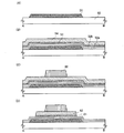
本実施の形態のボトムゲート構造のチャネルストップ型(チャネル保護型ともいう)薄膜トランジスタ74を図1に示す。
A channel stop type (also referred to as channel protection type)
図1において、基板50上に、ゲート電極51、ゲート絶縁膜52a、52b、微結晶半導体膜61、バッファ層62、チャネル保護層80、ソース領域及びドレイン領域72、ソース電極及びドレイン電極71a、71b、71cを含むチャネルストップ型薄膜トランジスタ74が設けられており、ソース電極及びドレイン電極71cに接して画素電極77が設けられている。薄膜トランジスタ74及び画素電極77の一部を覆うように絶縁膜76が設けられている。なお、図1は、図4(D)に対応している。
In FIG. 1, a
微結晶半導体膜61のチャネル形成領域上にバッファ層62を介してチャネル保護層80を設ける構造であるため、微結晶半導体膜61のチャネル形成領域上のバッファ層62に対する工程時におけるダメージ(エッチング時のプラズマやエッチング剤による膜減りや、酸化など)を防ぐことができる。従って薄膜トランジスタ74の信頼性を向上させることができる。また微結晶半導体膜61のチャネル形成領域上のバッファ層62がエッチングされないため、バッファ層62の膜厚を厚く形成する必要がなく成膜時間を短縮できる。
Since the channel
また、微結晶半導体膜61の端部は、ゲート絶縁膜52a、52bを介して重畳するゲート電極51の端部より内側であり、ゲート電極51上にすべての領域が収まるように形成されている。よって、微結晶半導体膜61は、ゲート電極51及びゲート絶縁膜52a、52b上の平坦な領域に形成することができるために、被覆性もよく、膜内において均一な特性(結晶状態)を有する膜とすることができる。
Further, the end portion of the
以下、作製方法を詳細に説明する。基板50上にゲート電極51を形成する(図2(A)及び図4(A)参照。)。図2(A)は、図4(A)のA−Bの断面図に相当する。基板50は、バリウムホウケイ酸ガラス、アルミノホウケイ酸ガラス、若しくはアルミノシリケートガラスなど、フュージョン法やフロート法で作製される無アルカリガラス基板、セラミック基板の他、本作製工程の処理温度に耐えうる耐熱性を有するプラスチック基板等を用いることができる。また、ステンレス合金などの金属基板の表面に絶縁膜を設けた基板を適用しても良い。基板50の大きさは、320mm×400mm、370mm×470mm、550mm×650mm、600mm×720mm、680mm×880mm、730mm×920mm、1000mm×1200mm、1100mm×1250mm、1150mm×1300mm、1500mm×1800mm、1900mm×2200mm、2160mm×2460mm、2400mm×2800mm、又は2850mm×3050mm等を用いることができる。
Hereinafter, the production method will be described in detail. A
ゲート電極51は、チタン、モリブデン、クロム、タンタル、タングステン、アルミニウムなどの金属材料またはその合金材料を用いて形成する。ゲート電極51は、スパッタリング法や真空蒸着法で基板50上に導電膜を形成し、当該導電膜上にフォトリソグラフィ技術またはインクジェット法によりマスクを形成し、当該マスクを用いて導電膜をエッチングすることで、形成することができる。また、銀、金、銅などの導電性ナノペーストを用いてインクジェット法により吐出し焼成して、ゲート電極51を形成することができる。なお、ゲート電極51の密着性向上と下地膜や基板への拡散を防ぐバリアメタルとして、上記金属材料の窒化物膜を、基板50及びゲート電極51の間に設けてもよい。また、ゲート電極51は積層構造としてもよく、基板50側からアルミニウム膜とモリブデン膜の積層、銅膜とモリブデン膜との積層、銅膜と窒化チタン膜との積層、銅膜と窒化タンタル膜との積層などを用いることができる。上記積層構造において、上層に形成されるモリブデン膜や、窒化チタン膜、窒化タンタル膜などの窒化物膜はバリアメタルとしての効果を有する。
The
なお、ゲート電極51上には半導体膜や配線を形成するので、段切れ防止のため端部がテーパー状になるように加工することが望ましい。また、図示しないがこの工程でゲート電極に接続する配線も同時に形成することができる。
Note that since a semiconductor film or a wiring is formed over the
次に、ゲート電極51上に、ゲート絶縁膜52a、52b、微結晶半導体膜53、バッファ層54を順に形成する(図2(B)参照。)。
Next,
微結晶半導体膜53を、水素プラズマを作用させつつ(作用させた)ゲート絶縁膜52b表面に形成してもよい。水素プラズマを作用させたゲート絶縁膜上に微結晶半導体膜を形成すると、微結晶の結晶成長を促進することができる。また、ゲート絶縁膜及び微結晶半導体膜の界面における格子歪を低減することが可能であり、ゲート絶縁膜及び微結晶半導体膜の界面特性を向上させることができる。従って得られる微結晶半導体膜は電気特性が高く信頼性のよいものとすることができる。
The
なお、ゲート絶縁膜52a、52b、微結晶半導体膜53、及びバッファ層54を大気に触れさせることなく連続的に形成してもよい。ゲート絶縁膜52a、52b、微結晶半導体膜53、及びバッファ層54を大気に触れさせることなく連続成膜することで、大気成分や大気中に浮遊する汚染不純物元素に汚染されることなく各積層界面を形成することができるので、薄膜トランジスタ特性のばらつきを低減することができる。
Note that the
ゲート絶縁膜52a、52bはそれぞれ、CVD法やスパッタリング法等を用いて、酸化珪素膜、窒化珪素膜、酸化窒化珪素膜、または窒化酸化珪素膜で形成することができる。ここでは、ゲート絶縁膜52a、52bとして、窒化珪素膜または窒化酸化珪素膜と、酸化珪素膜または酸化窒化珪素膜との順に積層して形成する形態を示す。なお、ゲート絶縁膜を2層とせず、基板側から窒化珪素膜または窒化酸化珪素膜と、酸化珪素膜または酸化窒化珪素膜と、窒化珪素膜または窒化酸化珪素膜との順に3層積層して形成することができる。また、ゲート絶縁膜を、酸化珪素膜、窒化珪素膜、酸化窒化珪素膜、または窒化酸化珪素膜の単層で形成することができる。更には、周波数が1GHz以上のマイクロ波プラズマCVD装置を用いてゲート絶縁膜を形成することが好ましい。マイクロ波プラズマCVD装置で形成した酸化窒化珪素膜、窒化酸化珪素膜は、耐圧が高く、後に形成される薄膜トランジスタの信頼性を高めることができる。
Each of the
ゲート絶縁膜の3層積層構造の例として、ゲート電極上に1層目として窒化珪素膜または窒化酸化珪素膜と、2層目として酸化窒化珪素膜と、3層目として窒化珪素膜とを積層とし、最上層の窒化珪素膜上に微結晶半導体膜を形成してもよい。この場合、1層目の窒化珪素膜または窒化酸化珪素膜は膜厚が50nmより厚い方がよく、ナトリウムなどの不純物を遮断するバリア、ゲート電極のヒロックの防止、ゲート電極の酸化防止などの効果を奏する。3層目の窒化珪素膜は微結晶半導体膜の密着性向上、微結晶半導体膜にレーザ照射を行うLP処理の際に酸化防止としての効果を奏する。 As an example of a three-layer structure of a gate insulating film, a silicon nitride film or a silicon nitride oxide film as a first layer, a silicon oxynitride film as a second layer, and a silicon nitride film as a third layer are stacked on the gate electrode A microcrystalline semiconductor film may be formed over the uppermost silicon nitride film. In this case, the thickness of the first silicon nitride film or silicon nitride oxide film is preferably larger than 50 nm, and effects such as a barrier that blocks impurities such as sodium, prevention of hillocks in the gate electrode, and prevention of oxidation of the gate electrode Play. The third silicon nitride film has an effect of improving the adhesion of the microcrystalline semiconductor film and preventing oxidation during LP treatment in which laser irradiation is performed on the microcrystalline semiconductor film.
このようにゲート絶縁膜表面に極薄膜の窒化珪素膜のような窒化膜を形成することで微結晶半導体膜の密着性を向上することができる。窒化膜はプラズマCVD法により成膜してもよく、マイクロ波による高密度で低温なプラズマ処理によって窒化処理を行ってもよい。また、反応室にシランフラッシュ処理を行う際に窒化珪素膜、窒化酸化珪素膜を形成してもよい。 Thus, by forming a nitride film such as an extremely thin silicon nitride film on the surface of the gate insulating film, the adhesion of the microcrystalline semiconductor film can be improved. The nitride film may be formed by a plasma CVD method, or nitridation may be performed by high-density and low-temperature plasma treatment using microwaves. Further, a silicon nitride film or a silicon nitride oxide film may be formed when the silane flash treatment is performed in the reaction chamber.
ここでは、酸化窒化珪素膜とは、その組成として、窒素よりも酸素の含有量が多いものであって、濃度範囲として酸素が55〜65原子%、窒素が1〜20原子%、Siが25〜35原子%、水素が0.1〜10原子%の範囲で含まれるものをいう。また、窒化酸化珪素膜とは、その組成として、酸素よりも窒素の含有量が多いものであって、濃度範囲として酸素が15〜30原子%、窒素が20〜35原子%、Siが25〜35原子%、水素が15〜25原子%の範囲で含まれるものをいう。 Here, the silicon oxynitride film has a composition that contains more oxygen than nitrogen and has a concentration range of 55 to 65 atomic%, 1 to 20 atomic%, and 25 Si. -35 atomic%, and hydrogen is contained in the range of 0.1-10 atomic%. The silicon nitride oxide film has a composition containing more nitrogen than oxygen, and the concentration ranges of oxygen are 15 to 30 atomic%, nitrogen is 20 to 35 atomic%, and Si is 25 to 25%. 35 atomic% and hydrogen are included in the range of 15 to 25 atomic%.
微結晶半導体膜53は、非晶質と結晶構造(単結晶、多結晶を含む)の中間的な構造の半導体を含む膜である。この半導体は、自由エネルギー的に安定な第3の状態を有する半導体であって、短距離秩序を持ち格子歪みを有する結晶質なものであり、その膜表面より見た粒径が0.5〜20nmの柱状または針状結晶が基板表面に対して法線方向に成長している。また、微結晶半導体と非晶質半導体とが混在している。微結晶半導体の代表例である微結晶シリコンは、そのラマンスペクトルが単結晶シリコンを示す521cm−1よりも低波数側に、シフトしている。即ち、単結晶シリコンを示す521cm−1とアモルファスシリコンを示す480cm−1の間に微結晶シリコンのラマンスペクトルのピークがある。また、未結合手(ダングリングボンド)を終端するため水素またはハロゲンを少なくとも1原子%またはそれ以上含ませている。さらに、ヘリウム、アルゴン、クリプトン、ネオンなどの希ガス元素を含ませて格子歪みをさらに助長させることで、安定性が増し良好な微結晶半導体膜が得られる。このような微結晶半導体膜に関する記述は、例えば、米国特許4,409,134号で開示されている。
The
この微結晶半導体膜は、周波数が数十MHz〜数百MHzの高周波プラズマCVD法、または周波数が1GHz以上のマイクロ波プラズマCVD装置により形成することができる。代表的には、SiH4、Si2H6、SiH2Cl2、SiHCl3、SiCl4、SiF4などの水素化珪素を水素で希釈して形成することができる。また、水素化珪素及び水素に加え、ヘリウム、アルゴン、クリプトン、ネオンから選ばれた一種または複数種の希ガス元素で希釈して微結晶半導体膜を形成することができる。これらのときの水素化珪素に対して水素の流量比を5倍以上200倍以下、好ましくは50倍以上150倍以下、更に好ましくは100倍とする。 This microcrystalline semiconductor film can be formed by a high-frequency plasma CVD method with a frequency of several tens to several hundreds of MHz or a microwave plasma CVD apparatus with a frequency of 1 GHz or more. Typically, silicon hydride such as SiH 4 , Si 2 H 6 , SiH 2 Cl 2 , SiHCl 3 , SiCl 4 , and SiF 4 can be formed by diluting with hydrogen. In addition to silicon hydride and hydrogen, the microcrystalline semiconductor film can be formed by dilution with one or more kinds of rare gas elements selected from helium, argon, krypton, and neon. The flow rate ratio of hydrogen to silicon hydride at these times is 5 to 200 times, preferably 50 to 150 times, and more preferably 100 times.
また、微結晶半導体膜は、価電子制御を目的とした不純物元素を意図的に添加しないときに弱いn型の電気伝導性を示すので、薄膜トランジスタのチャネル形成領域として機能する微結晶半導体膜に対しては、p型を付与する不純物元素を、成膜と同時に、或いは成膜後に添加することで、しきい値制御をすることが可能となる。p型を付与する不純物元素としては、代表的には硼素であり、B2H6、BF3などの不純物気体を1ppm〜1000ppm、好ましくは1〜100ppmの割合で水素化珪素に混入させると良い。そしてボロンの濃度を、例えば1×10¹⁴〜6×10¹⁶atoms/cm3とすると良い。 In addition, since the microcrystalline semiconductor film exhibits weak n-type conductivity when an impurity element for the purpose of controlling valence electrons is not intentionally added, the microcrystalline semiconductor film functions as a channel formation region of a thin film transistor. Thus, the threshold value can be controlled by adding an impurity element imparting p-type at the same time as film formation or after film formation. The impurity element imparting p-type is typically boron, and an impurity gas such as B 2 H 6 or BF 3 may be mixed into silicon hydride at a rate of 1 ppm to 1000 ppm, preferably 1 to 100 ppm. . The boron concentration is preferably 1 × 10 14 to 6 × 10 16 atoms / cm 3 , for example.
また、微結晶半導体膜の酸素濃度を、5×10¹⁹atoms/cm3以下、1×1019atoms/cm3以下、窒素及び炭素の濃度それぞれを1×1018atoms/cm3以下とすることが好ましい。酸素、窒素、及び炭素が微結晶半導体膜に混入する濃度を低減することで、微結晶半導体膜がn型化になることを防止することができる。 In addition, the oxygen concentration of the microcrystalline semiconductor film is 5 × 10 19 atoms / cm 3 or less, 1 × 10 19 atoms / cm 3 or less, and the nitrogen and carbon concentrations are 1 × 10 18 atoms / cm 3 or less. Is preferred. By reducing the concentration of oxygen, nitrogen, and carbon in the microcrystalline semiconductor film, the microcrystalline semiconductor film can be prevented from becoming n-type.
微結晶半導体膜53は、0nmより厚く50nm以下、好ましくは0nmより厚く20nm以下で形成する。
The
微結晶半導体膜53は後に形成される薄膜トランジスタのチャネル形成領域として機能する。微結晶半導体膜53の厚さを上記の範囲内とすることで、後に形成される薄膜トランジスタは、完全空乏型となる。また、微結晶半導体膜は微結晶で構成されているため、非晶質半導体膜と比較して抵抗が低い。このため、微結晶半導体膜を用いた薄膜トランジスタは、電流電圧特性を示す曲線の立ち上がり部分の傾きが急峻となり、スイッチング素子としての応答性が優れ、高速動作が可能となる。また、薄膜トランジスタのチャネル形成領域に微結晶半導体膜を用いることで、薄膜トランジスタの閾値の変動を抑制することが可能である。このため、電気特性のばらつきの少ない発光装置を作製することができる。
The
また、微結晶半導体膜は非晶質半導体膜と比較して移動度が高い。このため、表示素子のスイッチングとして、チャネル形成領域が微結晶半導体膜で形成される薄膜トランジスタを用いることで、チャネル形成領域の面積、即ち薄膜トランジスタの面積を縮小することが可能である。このため、一画素あたりに示す薄膜トランジスタの面積が小さくなり、画素の開口率を高めることが可能である。この結果、解像度の高い装置を作製することができる。 In addition, the microcrystalline semiconductor film has higher mobility than the amorphous semiconductor film. Therefore, the area of the channel formation region, that is, the area of the thin film transistor can be reduced by using a thin film transistor in which the channel formation region is formed using a microcrystalline semiconductor film for switching the display element. Therefore, the area of the thin film transistor shown per pixel is reduced, and the aperture ratio of the pixel can be increased. As a result, a device with high resolution can be manufactured.
また、微結晶半導体膜は下側から縦方向に成長し、針状結晶である。微結晶半導体膜には非晶質と結晶構造が混在しており、結晶領域と非晶質領域との間に局部応力でクラックが発生し、隙間ができやすい。この隙間に新たなラジカルが介入して結晶成長を起こしうる。しかし上方の結晶面が大きくなるため、針状に上方に成長しやすい。このように微結晶半導体膜は縦方向に成長しても、非晶質半導体膜の成膜速度に比べて1/10〜1/100の早さである。 The microcrystalline semiconductor film grows in the vertical direction from the lower side and is a needle-like crystal. A microcrystalline semiconductor film has both an amorphous structure and a crystalline structure, and a crack is generated by a local stress between the crystalline region and the amorphous region, so that a gap is easily formed. New radicals can intervene in this gap to cause crystal growth. However, since the upper crystal plane becomes large, it tends to grow upward in a needle shape. Thus, even if the microcrystalline semiconductor film is grown in the vertical direction, it is 1/10 to 1/100 faster than the deposition rate of the amorphous semiconductor film.
バッファ層54は、SiH4、Si2H6、SiH2Cl2、SiHCl3、SiCl4、SiF4などの珪素気体(水素化珪素気体、ハロゲン化珪素気体)を用いて、プラズマCVD法により形成することができる。また、上記シランに、ヘリウム、アルゴン、クリプトン、ネオンから選ばれた一種または複数種の希ガス元素で希釈して非晶質半導体膜を形成することができる。水素化珪素の流量の1倍以上20倍以下、好ましくは1倍以上10倍以下、更に好ましくは1倍以上5倍以下の流量の水素を用いて、水素を含む非晶質半導体膜を形成することができる。また、上記水素化珪素と窒素またはアンモニアとを用いることで、窒素を含む非晶質半導体膜を形成することができる。また、上記水素化珪素と、フッ素、塩素、臭素、またはヨウ素を含む気体(F2、Cl2、Br2、I2、HF、HCl、HBr、HI等)を用いることで、フッ素、塩素、臭素、またはヨウ素を含む非晶質半導体膜を形成することができる。
The
また、バッファ層54は、ターゲットに非晶質半導体を用いて水素、または希ガスでスパッタリングして非晶質半導体膜を形成することができる。このとき、アンモニア、窒素、またはN2Oを雰囲気中に含ませることにより、窒素を含む非晶質半導体膜を形成することができる。また、雰囲気中にフッ素、塩素、臭素、またはヨウ素を含む気体(F2、Cl2、Br2、I2、HF、HCl、HBr、HI等)を含ませることにより、フッ素、塩素、臭素、またはヨウ素を含む非晶質半導体膜を形成することができる。
The
また、バッファ層54として、微結晶半導体膜53の表面にプラズマCVD法またはスパッタリング法により非晶質半導体膜を形成した後、非晶質半導体膜の表面を水素プラズマ、窒素プラズマ、またはハロゲンプラズマ、希ガス(ヘリウム、アルゴン、クリプトン、ネオン)によるプラズマで処理して、非晶質半導体膜の表面を水素化、窒素化、またはハロゲン化してもよい。
As the
バッファ層54は、非晶質半導体膜で形成することが好ましい。このため、周波数が数十MHz〜数百MHzの高周波プラズマCVD法、またはマイクロ波プラズマCVD法で形成する場合は、非晶質半導体膜となるように、成膜条件を制御することが好ましい。
The
バッファ層54は、代表的には、10nm以上50nm以下の厚さで形成することが好ましい。また、バッファ層に含まれる窒素、炭素、及び酸素の総濃度を1×10²⁰atoms/cm3〜15×1020atoms/cm3とすることが好ましい。上記濃度であれば膜厚が10nm以上50nm以下であってもバッファ層54を、高抵抗領域として機能させることできる。
The
バッファ層54を、膜厚を150nm以上200nm以下とし、含まれる炭素、窒素、酸素のそれぞれの濃度は、3×10¹⁹atoms/cm3以下、好ましくは5×1018atoms/cm3以下としてもよい。
The
微結晶半導体膜53の表面に、バッファ層として非晶質半導体膜、又は水素、窒素、またはハロゲンを含む非晶質半導体膜を形成することで、微結晶半導体膜53に含まれる結晶粒の表面の自然酸化を防止することが可能である。微結晶半導体膜53の表面にバッファ層を形成することで、微結晶粒の酸化を防ぐことができる。バッファ層には水素、及び/又は、フッ素が混入していることにより、酸素が微結晶半導体膜に進入することを防止する効果がある。
By forming an amorphous semiconductor film or an amorphous semiconductor film containing hydrogen, nitrogen, or halogen as a buffer layer over the surface of the
また、バッファ層54は、非晶質半導体膜を用いて、または、水素、窒素、若しくはハロゲンを含む非晶質半導体膜を用いて形成するため、チャネル形成領域として機能する微結晶半導体膜よりも抵抗が高い。このため、後に形成される薄膜トランジスタにおいて、ソース領域及びドレイン領域と、微結晶半導体膜との間に形成されるバッファ層は高抵抗領域として機能する。このため、薄膜トランジスタのオフ電流を低減することができる。当該薄膜トランジスタを発光装置のスイッチング素子として用いた場合、発光装置のコントラストを向上させることができる。
Further, since the
次にバッファ層54において微結晶半導体膜53のチャネル形成領域と重畳する領域にチャネル保護層80を形成する(図2(C)参照。)。チャネル保護層80もゲート絶縁膜52a、52b、微結晶半導体膜53、バッファ層54と大気に触れさせずに連続成膜することによって形成してもよい。積層する薄膜を大気に曝さずに連続的に成膜すると生産性が向上する。
Next, a channel
チャネル保護層80としては、無機材料(酸化珪素、窒化珪素、酸化窒化珪素、窒化酸化珪素など)を用いることができる。感光性または非感光性の有機材料(有機樹脂材料)(ポリイミド、アクリル、ポリアミド、ポリイミドアミド、レジスト、ベンゾシクロブテンなど)、もしくは複数種からなる膜、またはこれらの膜の積層などを用いることができる。また、シロキサンを用いてもよい。作製法としては、プラズマCVD法や熱CVD法などの気相成長法やスパッタリング法を用いることができる。また、湿式法である、スピンコート法などの塗布法、液滴吐出法や、印刷法(スクリーン印刷やオフセット印刷などパターンが形成される方法)を用いることもできる。チャネル保護層80は成膜後にエッチングにより形状を加工して形成してもよいし、液滴吐出法などによって選択的に形成してもよい。
As the channel
次に微結晶半導体膜53及びバッファ層54をエッチングにより加工し、微結晶半導体膜61及びバッファ層62の積層を形成する(図2(D)参照。)。微結晶半導体膜61及びバッファ層62は、フォトリソグラフィ技術または液滴吐出法によりマスクを形成し、当該マスクを用いて微結晶半導体膜53及びバッファ層54をエッチングすることで、形成することができる。なお、図2(D)は、図4(B)のA−Bの断面図に相当する。
Next, the
微結晶半導体膜61、バッファ層62の端部をテーパーを有する形状にエッチングすることができる。その端部のテーパー角は90°〜30°、好ましくは80°〜45°とする。これにより、段差形状による配線の段切れを防ぐことができる。
The ends of the
次に、ゲート絶縁膜52b、微結晶半導体膜61、バッファ層62、チャネル保護層80上に一導電型を付与する不純物が添加された半導体膜63及び導電膜65a〜65cを形成する(図3(A)参照。)。一導電型を付与する不純物が添加された半導体膜63及び導電膜65a〜65c上にマスク66を形成する。マスク66は、フォトリソグラフィ技術またはインクジェット法により形成する。
Next, a
一導電型を付与する不純物が添加された半導体膜63は、nチャネル型の薄膜トランジスタを形成する場合には、代表的な不純物元素としてリンを添加すれば良く、水素化珪素にPH3などの不純物気体を加えれば良い。また、pチャネル型の薄膜トランジスタを形成する場合には、代表的な不純物元素としてボロンを添加すれば良く、水素化珪素にB2H6などの不純物気体を加えれば良い。一導電型を付与する不純物が添加された半導体膜63は、微結晶半導体膜、または非晶質半導体膜で形成することができる。一導電型を付与する不純物が添加された半導体膜63は膜厚2〜50nm(好ましくは10〜30nm)とすればよい。
In the case of forming an n-channel thin film transistor, the
導電膜は、アルミニウム、銅、若しくはシリコン、チタン、ネオジム、スカンジウム、モリブデンなどの耐熱性向上元素若しくはヒロック防止元素が添加されたアルミニウム合金の単層または積層で形成することが好ましい。また、一導電型を付与する不純物が添加された半導体膜と接する側の膜を、チタン、タンタル、モリブデン、タングステン、またはこれらの元素の窒化物で形成し、その上にアルミニウムまたはアルミニウム合金を形成した積層構造としても良い。更には、アルミニウムまたはアルミニウム合金の上面及び下面を、チタン、タンタル、モリブデン、タングステン、またはこれらの元素の窒化物で挟んだ積層構造としてもよい。ここでは、導電膜としては、導電膜65a〜65c3層が積層した構造の導電膜を示し、導電膜65a、65cにモリブデン膜、導電膜65bにアルミニウム膜を用いた積層導電膜や、導電膜65a、65cにチタン膜、導電膜65bにアルミニウム膜を用いた積層導電膜を示す。
The conductive film is preferably formed using a single layer or a stack of aluminum, copper, or an aluminum alloy to which a heat resistance improving element such as silicon, titanium, neodymium, scandium, or molybdenum or a hillock preventing element is added. In addition, a film in contact with a semiconductor film to which an impurity imparting one conductivity type is added is formed using titanium, tantalum, molybdenum, tungsten, or a nitride of these elements, and aluminum or an aluminum alloy is formed thereover. It is good also as a laminated structure. Furthermore, a laminated structure in which the upper and lower surfaces of aluminum or an aluminum alloy are sandwiched between titanium, tantalum, molybdenum, tungsten, or nitrides of these elements may be employed. Here, a conductive film having a structure in which
導電膜65a〜65cは、スパッタリング法や真空蒸着法で形成する。また、導電膜65a〜65cは、銀、金、銅などの導電性ナノペーストを用いてスクリーン印刷法、インクジェット法等を用いて吐出し焼成して形成しても良い。
The
次に、マスク66を用いて導電膜65a〜65cをエッチングし分離して、ソース電極及びドレイン電極71a〜71cを形成する(図3(B)参照。)。本実施の形態の図3(B)のように導電膜65a〜65cをウエットエッチングすると、導電膜65a〜65cは等方的にエッチングされるため、マスク66の端部と、ソース電極及びドレイン電極71a〜71cの端部はより一致せずより後退している。次に、マスク66を用いて一導電型を付与する不純物が添加された半導体膜63をエッチングして、ソース領域及びドレイン領域72を形成する(図3(C)参照。)。なお、バッファ層62はチャネル保護層80がチャネルストッパーとして機能するためエッチングされない。
Next, the
ソース電極及びドレイン電極71a〜71cの端部と、ソース領域及びドレイン領域72の端部は一致せずずれており、ソース電極及びドレイン電極71a〜71cの端部の外側に、ソース領域及びドレイン領域72の端部が形成される。この後、マスク66を除去する。なお、図3(C)は、図4(C)のA−Bの断面図に相当する。図4(C)に示すように、ソース領域及びドレイン領域72の端部は、ソース電極及びドレイン電極71a〜71cの端部の外側に位置することが分かる。また、ソース領域及びドレイン領域72の面積は、ソース電極及びドレイン電極71a〜71cの面積よりも広いことが分かる。また、ソース電極またはドレイン電極の一方は、ソース配線またはドレイン配線としても機能する。
The end portions of the source and
図3(C)に示すように、ソース電極及びドレイン電極71a〜71cの端部と、ソース領域及びドレイン領域72の端部は一致せずずれた形状となることで、ソース電極及びドレイン電極71a〜71cの端部の距離が離れるため、ソース電極及びドレイン電極間のリーク電流やショートを防止することができる。また、ソース領域及びドレイン領域は、ソース電極及びドレイン電極の端よりも延びており、対向するソース領域とドレイン領域の距離は、対向するソース電極とドレイン領域の距離よりも短い。このため、信頼性が高く、且つ耐圧の高い薄膜トランジスタを作製することができる。
As shown in FIG. 3C, the end portions of the source and
以上の工程により、チャネルストップ(保護)型の薄膜トランジスタ74を形成することができる。
Through the above steps, a channel stop (protective)
バッファ層62は、ソース領域及びドレイン領域72下のバッファ層62と微結晶半導体膜61のチャネル形成領域上のバッファ層62は同一材料であり同時に形成される連続膜である。微結晶半導体膜61上のバッファ層62は含まれる水素によって外部の空気、エッチング残渣を遮断し、微結晶半導体膜61を保護する。
The
一導電型を付与する不純物を含まないバッファ層62を設けることによって、ソース領域及びドレイン領域に含まれる一導電型を付与する不純物と微結晶半導体膜61のしきい値電圧制御用の一導電型を付与する不純物が相互に混ざらないようにすることができる。一導電型を付与する不純物が混ざると再結合中心ができ、リーク電流が流れてしまい、オフ電流低減の効果が得られなくなってしまう。
By providing the
以上のようにバッファ層及びチャネル保護層を設けることにより、リーク電流が低減された高耐圧のチャネルストップ型薄膜トランジスタを作製することができる。従って、5Vの電圧を印加する発光装置に用いる薄膜トランジスタの場合でも信頼性が高く好適に用いることができる。 By providing the buffer layer and the channel protective layer as described above, a high-breakdown-voltage channel stop thin film transistor with reduced leakage current can be manufactured. Therefore, even in the case of a thin film transistor used for a light-emitting device to which a voltage of 5 V is applied, the thin film transistor can be preferably used with high reliability.
次に、ソース電極またはドレイン電極71a〜71cに接する画素電極77を形成する。ソース電極及びドレイン電極71a〜71c、ソース領域及びドレイン領域72、チャネル保護層80、ゲート絶縁膜52b、及び画素電極77上に絶縁膜76を形成する。絶縁膜76は、ゲート絶縁膜52a、52bと同様に形成することができる。なお、絶縁膜76は、大気中に浮遊する有機物や金属物、水蒸気などの汚染不純物の侵入を防ぐためのものであり、緻密な膜が好ましい。
Next, the
バッファ層62は、代表的には、10nm以上50nm以下の厚さで形成することが好ましい。また、バッファ層に含まれる窒素、炭素、及び酸素の総濃度を1×10²⁰atoms/cm3〜15×1020atoms/cm3とすることが好ましい。上記濃度であれば膜厚が10nm以上50nm以下であってもバッファ層62を、高抵抗領域として機能させることできる。
The
しかし、バッファ層62を、膜厚を150nm以上200nm以下とし、含まれる炭素、窒素、酸素の濃度は、3×10¹⁹atoms/cm3以下、好ましくは5×1018atoms/cm3以下としてもよい。この場合、絶縁膜76に窒化珪素膜を用いることで、バッファ層62中の酸素濃度を5×1019atoms/cm3以下、好ましくは1×1019atoms/cm3以下とすることができる。
However, the
次に、絶縁膜76をエッチングし画素電極77の一部を露出する。画素電極77の露出領域に接するように発光素子を形成し、薄膜トランジスタ74と発光素子を電気的に接続することができる。例えば、画素電極77上に発光層を形成し、発光層上に対向電極を形成すればよい。
Next, the insulating
画素電極77は、酸化タングステンを含むインジウム酸化物、酸化タングステンを含むインジウム亜鉛酸化物、酸化チタンを含むインジウム酸化物、酸化チタンを含むインジウム錫酸化物、インジウム錫酸化物(以下、ITOと示す。)、インジウム亜鉛酸化物、酸化ケイ素を添加したインジウム錫酸化物などの透光性を有する導電性材料を用いることができる。
The
また、画素電極77として、導電性高分子(導電性ポリマーともいう)を含む導電性組成物を用いて形成することができる。導電性組成物を用いて形成した画素電極は、シート抵抗が10000Ω/□以下、波長550nmにおける透光率が70%以上であることが好ましい。また、導電性組成物に含まれる導電性高分子の抵抗率が0.1Ω・cm以下であることが好ましい。
The
導電性高分子としては、いわゆるπ電子共役系導電性高分子が用いることができる。例えば、ポリアニリンまたはその誘導体、ポリピロールまたはその誘導体、ポリチオフェンまたはその誘導体、若しくはこれらの2種以上の共重合体などがあげられる。 As the conductive polymer, a so-called π-electron conjugated conductive polymer can be used. For example, polyaniline or a derivative thereof, polypyrrole or a derivative thereof, polythiophene or a derivative thereof, or a copolymer of two or more kinds thereof can be given.
また、ソース領域及びドレイン領域の端部とソース電極及びドレイン電極の端部を一致する形状としてもよい。図14にソース領域及びドレイン領域の端部とソース電極及びドレイン電極の端部が一致する形状のチャネルストップ型の薄膜トランジスタ79を示す。ソース電極及びドレイン電極のエッチング及びソース領域及びドレイン領域のエッチングをドライエッチングで行うと薄膜トランジスタ79のような形状にすることができる。また、一導電型を付与する不純物が添加された半導体膜をソース電極及びドレイン電極をマスクとしてエッチングし、ソース領域及びドレイン領域を形成しても薄膜トランジスタ79のような形状にすることができる。
Alternatively, the end portions of the source region and the drain region may coincide with the end portions of the source electrode and the drain electrode. FIG. 14 shows a channel stop type
チャネルストップ型の薄膜トランジスタとすることで薄膜トランジスタの信頼性を向上させることができる。また、微結晶半導体膜でチャネル形成領域を構成することにより1〜20cm2/V・secの電界効果移動度を得ることができる。従って、この薄膜トランジスタを画素部の画素のスイッチング用素子として、さらに走査線(ゲート線)側の駆動回路を形成する素子として利用することができる。 By using a channel stop thin film transistor, the reliability of the thin film transistor can be improved. Further, field effect mobility of 1 to 20 cm 2 / V · sec can be obtained by forming a channel formation region using a microcrystalline semiconductor film. Therefore, this thin film transistor can be used as an element for switching a pixel in the pixel portion and an element for forming a driving circuit on the scanning line (gate line) side.
本実施の形態により、電気特性が高く信頼性のよい薄膜トランジスタを有する発光装置を作製することができる。 According to this embodiment, a light-emitting device having a thin film transistor with high electrical characteristics and high reliability can be manufactured.
(実施の形態2)
本実施の形態は、実施の形態1において、薄膜トランジスタの形状が異なる例である。従って、他は実施の形態1と同様に行うことができ、実施の形態1と同一部分又は同様な機能を有する部分、及び工程の繰り返しの説明は省略する。
(Embodiment 2)
This embodiment is an example in which the shape of a thin film transistor is different from that in
本実施の形態では、発光装置に用いられる薄膜トランジスタ及びその作製工程について、図5、図6及び図15を用いて説明する。図5及び図15は、薄膜トランジスタ及び画素電極を示す断面図であり、図6は一画素における薄膜トランジスタ及び画素電極の接続領域の平面図である。図5及び図15は、図6における線Q−Rの薄膜トランジスタ及びその作製工程を示す断面図に相当する。 In this embodiment, a thin film transistor used for a light-emitting device and a manufacturing process thereof will be described with reference to FIGS. 5 and 15 are cross-sectional views showing the thin film transistor and the pixel electrode, and FIG. 6 is a plan view of a connection region of the thin film transistor and the pixel electrode in one pixel. 5 and 15 correspond to cross-sectional views illustrating the thin film transistor taken along line QR in FIG. 6 and a manufacturing process thereof.
本実施の形態のボトムゲート構造のチャネルストップ型(チャネル保護型ともいう)薄膜トランジスタ274を図5及び図6に示す。
A channel stop type (also referred to as channel protection type)
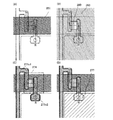
図5において、基板250上に、ゲート電極251、ゲート絶縁膜252a、252b、微結晶半導体膜261、バッファ層262、チャネル保護層280、ソース領域及びドレイン領域272、ソース電極及びドレイン電極271a、271b、271cを含むチャネルストップ型薄膜トランジスタ274が設けられており、薄膜トランジスタ274を覆うように絶縁膜276が設けられている。絶縁膜276に形成されたコンタクトホールにおいてソース電極及びドレイン電極271cに接して画素電極277が設けられている。なお、図5は、図6(D)に対応している。
In FIG. 5, a
微結晶半導体膜261のチャネル形成領域上にバッファ層262を介してチャネル保護層280を設ける構造であるため、微結晶半導体膜261のチャネル形成領域上のバッファ層262に対する工程時におけるダメージ(エッチング時のプラズマによるラジカルやエッチング剤による膜減りや、酸化など)を防ぐことができる。従って薄膜トランジスタ274の信頼性を向上させることができる。また微結晶半導体膜261のチャネル形成領域上のバッファ層262がエッチングされないため、バッファ層262の膜厚を厚く形成する必要がなく成膜時間を短縮できる。
Since the channel
以下、作製方法を図6(A)乃至(D)を用いて説明する。基板250上にゲート電極251を形成する(図6(A)参照。)。ゲート電極251上にゲート絶縁膜252a、252bを形成し、微結晶半導体膜261、バッファ層262を形成する。バッファ層262において、微結晶半導体膜のチャネル形成領域と重畳する領域にチャネル保護層280を形成する(図6(B)参照。)。
Hereinafter, a manufacturing method will be described with reference to FIGS. A
実施の形態1では、チャネル保護層80を形成後、微結晶半導体膜53とバッファ層54を島状の微結晶半導体膜61及びバッファ層62にエッチング工程により加工する例を示したが、本実施の形態では、微結晶半導体膜及びバッファ層のエッチング工程もソース電極及びドレイン電極及び一導電型を付与する不純物が添加された半導体膜と同工程で行う例を示す。従って、微結晶半導体膜、バッファ層、一導電型を付与する不純物が添加された半導体膜、ソース電極及びドレイン電極は同じ形状を反映して形成される。このようにエッチング工程を一度に行うと、工程数が簡略化される上、エッチング工程に用いるマスクの数も減らすことができる。
In
微結晶半導体膜、バッファ層、一導電型を付与する不純物が添加された半導体膜、導電膜をエッチングし、微結晶半導体膜261、バッファ層262、ソース領域及びドレイン領域272、ソース電極及びドレイン電極271a乃至271cを形成し、チャネルストップ型の薄膜トランジスタ274を形成する(図6(C)参照。)。薄膜トランジスタ274上を覆う絶縁膜276を形成しソース電極及びドレイン電極271cに達するコンタクトホールを形成する。コンタクトホールに画素電極277を形成し、薄膜トランジスタ274と画素電極277を電気的に接続する(図6(D)参照。)。
The microcrystalline semiconductor film, the buffer layer, the semiconductor film to which an impurity imparting one conductivity type is added, the conductive film are etched, the
また、ソース領域及びドレイン領域の端部とソース電極及びドレイン電極の端部を一致する形状としてもよい。図15にソース領域及びドレイン領域の端部とソース電極及びドレイン電極の端部が一致する形状のチャネルストップ型の薄膜トランジスタ279を示す。ソース電極及びドレイン電極のエッチング及びソース領域及びドレイン領域のエッチングをドライエッチングで行うと薄膜トランジスタ279のような形状にすることができる。また、一導電型を付与する不純物が添加された半導体膜をソース電極及びドレイン電極をマスクとしてエッチングし、ソース領域及びドレイン領域を形成しても薄膜トランジスタ279のような形状にすることができる。
Alternatively, the end portions of the source region and the drain region may coincide with the end portions of the source electrode and the drain electrode. FIG. 15 illustrates a channel stop
チャネルストップ型の薄膜トランジスタとすることで薄膜トランジスタの信頼性を向上させることができる。また、微結晶半導体膜でチャネル形成領域を構成することにより1〜20cm2/V・secの電界効果移動度を得ることができる。従って、この薄膜トランジスタを画素部の画素のスイッチング用素子として、さらに走査線(ゲート線)側の駆動回路を形成する素子として利用することができる。 By using a channel stop thin film transistor, the reliability of the thin film transistor can be improved. Further, field effect mobility of 1 to 20 cm 2 / V · sec can be obtained by forming a channel formation region using a microcrystalline semiconductor film. Therefore, this thin film transistor can be used as an element for switching a pixel in the pixel portion and an element for forming a driving circuit on the scanning line (gate line) side.
本実施の形態により、電気特性が高く信頼性のよい薄膜トランジスタを有する発光装置を作製することができる。 According to this embodiment, a light-emitting device having a thin film transistor with high electrical characteristics and high reliability can be manufactured.
(実施の形態3)
本実施の形態では、微結晶半導体膜にレーザ光を照射する作製工程例を説明する。
(Embodiment 3)
In this embodiment, an example of a manufacturing process in which a microcrystalline semiconductor film is irradiated with laser light will be described.
基板上にゲート電極を形成し、ゲート電極を覆うようにゲート絶縁膜を形成する。そしてゲート絶縁膜上に微結晶半導体膜として微結晶シリコン(SAS)膜を堆積する。微結晶半導体膜の膜厚は1nm以上15nm未満、より好ましくは2nm以上10nm以下とすればよい。特に膜厚5nm(4〜8nm)であると、レーザ光に対して吸収率が高いため、生産性が向上する。 A gate electrode is formed on the substrate, and a gate insulating film is formed so as to cover the gate electrode. Then, a microcrystalline silicon (SAS) film is deposited as a microcrystalline semiconductor film over the gate insulating film. The thickness of the microcrystalline semiconductor film may be greater than or equal to 1 nm and less than 15 nm, more preferably greater than or equal to 2 nm and less than or equal to 10 nm. In particular, when the film thickness is 5 nm (4 to 8 nm), the absorptance is high with respect to laser light, and thus productivity is improved.
ゲート絶縁膜上にプラズマCVD法等で微結晶半導体膜を成膜しようとする場合、ゲート絶縁膜と、結晶を含む半導体膜との界面付近に、半導体膜よりも非晶質成分を多く含む領域(ここでは界面領域と呼ぶ)が形成されることがある。また、プラズマCVD法等で膜厚10nm程度以下の極薄い微結晶半導体膜を成膜しようとする場合、微結晶粒を含む半導体膜を形成することはできるが、膜全体に渡って均一に良質の微結晶粒を含む半導体膜を得ることは困難である。これらの場合において、以下に示すレーザ光を照射するレーザ処理は有効である。 When a microcrystalline semiconductor film is to be formed over the gate insulating film by a plasma CVD method or the like, a region that contains more amorphous components than the semiconductor film in the vicinity of the interface between the gate insulating film and the semiconductor film containing crystals (Referred to herein as the interface region) may be formed. In addition, when an ultra-thin microcrystalline semiconductor film having a thickness of about 10 nm or less is formed by plasma CVD or the like, a semiconductor film including microcrystalline grains can be formed, but the quality is uniformly uniform over the entire film. It is difficult to obtain a semiconductor film containing microcrystalline grains. In these cases, the following laser treatment for irradiating with laser light is effective.
次いで、微結晶シリコン膜の表面側からレーザ光を照射する。レーザ光は、微結晶シリコン膜が溶融しないエネルギー密度で照射する。すなわち、本実施の形態によるレーザ処理(Laser Process、以下「LP」ともいう。)は、輻射加熱により微結晶シリコン膜を溶融させないで行う固相結晶成長によるものである。すなわち、堆積された微結晶シリコン膜が液相にならない臨界領域を利用するものであり、その意味において「臨界成長」ともいうことができる。 Next, laser light is irradiated from the surface side of the microcrystalline silicon film. The laser light is irradiated at an energy density that does not melt the microcrystalline silicon film. In other words, laser processing (hereinafter also referred to as “LP”) according to the present embodiment is based on solid-phase crystal growth performed without melting the microcrystalline silicon film by radiation heating. That is, a critical region where the deposited microcrystalline silicon film does not become a liquid phase is used. In this sense, it can also be referred to as “critical growth”.
レーザ光は微結晶シリコン膜とゲート絶縁膜の界面にまで作用させることができる。それにより、微結晶シリコン膜の表面側における結晶を種として、該表面からゲート絶縁膜の界面に向けて固相結晶成長が進み略柱状の結晶が成長する。LP処理による固相結晶成長は、結晶粒径を拡大させるものではなく、むしろ膜の厚さ方向における結晶性を改善するものである。 Laser light can be applied to the interface between the microcrystalline silicon film and the gate insulating film. Thereby, using the crystals on the surface side of the microcrystalline silicon film as a seed, solid-phase crystal growth proceeds from the surface toward the interface of the gate insulating film, and a substantially columnar crystal grows. Solid phase crystal growth by LP treatment does not increase the crystal grain size, but rather improves the crystallinity in the thickness direction of the film.
LP処理は矩形長尺状に集光(線状レーザ光)することで、例えば730mm×920mmのガラス基板上の微結晶シリコン膜を1回のレーザ光スキャンで処理することができる。この場合、線状レーザ光を重ね合わせる割合(オーバーラップ率)を0〜90%(好ましくは0〜67%)として行う。これにより、基板1枚当たりの処理時間が短縮され、生産性を向上させることができる。レーザ光の形状は線状に限定されるものでなく面状としても同様に処理することができる。また、本LP処理は前記ガラス基板のサイズに限定されず、さまざまなものに適用することができる。 In the LP process, by focusing (linear laser light) into a rectangular shape, for example, a microcrystalline silicon film on a glass substrate of 730 mm × 920 mm can be processed by one laser light scan. In this case, the ratio of overlapping linear laser beams (overlap ratio) is set to 0 to 90% (preferably 0 to 67%). Thereby, the processing time per substrate can be shortened and productivity can be improved. The shape of the laser beam is not limited to a linear shape, and it can be similarly processed even if it is a planar shape. Further, the present LP treatment is not limited to the size of the glass substrate, and can be applied to various things.
LP処理により、ゲート絶縁膜界面領域の結晶性が改善され、本実施の形態の薄膜トランジスタのようなボトムゲート構造を有する薄膜トランジスタの電気的特性を向上させる作用を奏する。 By the LP treatment, the crystallinity of the interface region of the gate insulating film is improved, and the electrical characteristics of a thin film transistor having a bottom gate structure such as the thin film transistor of this embodiment are improved.
このような臨界成長においては、従来の低温ポリシリコンで見られた表面の凹凸(リッジと呼ばれる凸状体)が形成されず、LP処理後のシリコン表面は平滑性が保たれていることも特徴である。 In such critical growth, the surface irregularities (convex bodies called ridges) found in conventional low-temperature polysilicon are not formed, and the silicon surface after LP treatment is also maintained smooth. It is.
本実施の形態におけるように、成膜後の微結晶シリコン膜に直接的にレーザ光を作用させて得られる結晶性のシリコン膜は、従来における堆積されたままの微結晶シリコン膜、伝導加熱により改質された微結晶シリコン膜(上記非特許文献1におけるもの)とは、その成長メカニズム及び膜質が明らかに異なっている。本明細書では、成膜後の微結晶半導体膜にLP処理を行って得られる結晶性の半導体膜をLPSAS膜と呼ぶ。 As in this embodiment mode, a crystalline silicon film obtained by directly applying a laser beam to a microcrystalline silicon film after film formation is a conventional microcrystalline silicon film that has been deposited. The growth mechanism and film quality are clearly different from the modified microcrystalline silicon film (in Non-Patent Document 1). In this specification, a crystalline semiconductor film obtained by performing LP treatment on a microcrystalline semiconductor film after deposition is referred to as an LPSAS film.
LPSAS膜などの微結晶半導体膜を形成した後、プラズマCVD法によりバッファ層として非晶質シリコン(a−Si:H)膜を300℃〜400℃の温度にて成膜する。この成膜処理により水素がLPSAS膜に供給され、LPSAS膜の水素化をしたのと同等の効果が得られる。すなわち、LPSAS膜上に非晶質シリコン膜を堆積することにより、LPSAS膜に水素を拡散させてダングリングボンドの終端をすることができる。 After forming a microcrystalline semiconductor film such as an LPSAS film, an amorphous silicon (a-Si: H) film is formed at a temperature of 300 ° C. to 400 ° C. as a buffer layer by a plasma CVD method. By this film forming process, hydrogen is supplied to the LPSAS film, and the same effect as that obtained by hydrogenating the LPSAS film can be obtained. That is, by depositing an amorphous silicon film on the LPSAS film, hydrogen can be diffused into the LPSAS film to terminate dangling bonds.
以降の工程は、実施の形態1と同様に従って、チャネル保護層を形成し、その上にマスクを形成する。次に、マスクを用いて微結晶半導体膜、及びバッファ層をエッチングし分離する。次いで、一導電型を付与する不純物が添加された半導体膜を形成し、導電膜を形成し、その導電膜上にマスクを形成する。次に、そのマスクを用いて導電膜をエッチングし分離して、ソース電極及びドレイン電極を形成する。さらに同じマスクを用いてチャネル保護層をエッチングストッパーとしてエッチングし、ソース領域及びドレイン領域を形成する。 In the subsequent steps, a channel protective layer is formed and a mask is formed thereon in the same manner as in the first embodiment. Next, the microcrystalline semiconductor film and the buffer layer are etched and separated using a mask. Next, a semiconductor film to which an impurity imparting one conductivity type is added is formed, a conductive film is formed, and a mask is formed over the conductive film. Next, the conductive film is etched and separated using the mask to form a source electrode and a drain electrode. Further, using the same mask, the channel protective layer is etched as an etching stopper to form a source region and a drain region.
以上の工程により、チャネルストップ型の薄膜トランジスタを形成することができ、チャネルストップ型の薄膜トランジスタを有する発光装置を作製することができる。 Through the above steps, a channel stop thin film transistor can be formed, and a light-emitting device having a channel stop thin film transistor can be manufactured.
また、本実施の形態は、実施の形態1又は実施の形態2と自由に組み合わせることができる。
Further, this embodiment can be freely combined with
(実施の形態4)
本実施の形態は、実施の形態1乃至3において、発光装置の作製工程の例を詳細に説明する。従って、実施の形態1乃至3と同一部分又は同様な機能を有する部分、及び工程の繰り返しの説明は省略する。
(Embodiment 4)
In this embodiment, an example of a manufacturing process of a light-emitting device in
実施の形態1乃至3において、微結晶半導体膜を形成する前に、反応室のクリーニング、及びフラッシング(洗浄)処理(水素をフラッシュ物質として用いた水素フラッシュ、シランをフラッシュ物質として用いたシランフラッシュなど)を行ってもよい。フラッシング処理により、反応室の酸素、窒素、フッ素などの不純物による成膜する膜への汚染を防ぐことができる。
In
フラッシング処理により、反応室の酸素、窒素、フッ素などの不純物を除去することができる。例えば、プラズマCVD装置を用いて、モノシランをフラッシュ物質として用い、ガス流量8〜10SLMをチャンバーに5〜20分間、好ましくは10分〜15分間導入し続けることでシランフラッシュ処理を行う。なお、1SLMは1000sccm、即ち、0.06m3/hである。 By the flushing treatment, impurities such as oxygen, nitrogen, and fluorine in the reaction chamber can be removed. For example, using a plasma CVD apparatus, monosilane is used as a flash substance, and a silane flash process is performed by continuously introducing a gas flow rate of 8 to 10 SLM into the chamber for 5 to 20 minutes, preferably 10 to 15 minutes. Note that 1 SLM is 1000 sccm, that is, 0.06 m 3 / h.
クリーニングは、例えばフッ素ラジカルで行うことができる。なお、フッ素ラジカルは、反応室の外側に設けられたプラズマ発生器に、フッ化炭素、フッ化窒素、またはフッ素を導入し、解離し、フッ素ラジカルを反応室に導入することで、反応室内をクリーニングすることができる。 Cleaning can be performed with, for example, fluorine radicals. Fluorine radicals are introduced into a plasma generator provided outside the reaction chamber by introducing carbon fluoride, nitrogen fluoride, or fluorine, dissociated, and introducing fluorine radicals into the reaction chamber. Can be cleaned.
フラッシング処理は、ゲート絶縁膜、バッファ層、チャネル保護層、一導電型を付与する不純物が添加された半導体膜の成膜前にも行ってもよい。なお、フラッシング処理はクリーニング後に行うと効果的である。 The flushing treatment may be performed before forming the gate insulating film, the buffer layer, the channel protective layer, and the semiconductor film to which an impurity imparting one conductivity type is added. The flushing process is effective when performed after cleaning.
反応室は基板を搬入して成膜する前に、各反応室の内壁を成膜する種類の膜で保護膜を形成し、コーティングする(プリコート処理ともいう)を行ってよい。プリコート処理は反応室内に成膜ガスを流しプラズマ処理することによって、あらかじめ反応室内を保護膜によって薄く覆う処理である。例えば、微結晶半導体膜として微結晶シリコン膜を形成する前に、反応室内を0.2〜0.4μmの非晶質シリコン膜で覆うプリコート処理を行えばよい。プリコート処理後にもフラッシング処理(水素フラッシュ、シランフラッシュなど)を行ってもよい。クリーニング処理及びプリコート処理を行う場合は反応室内より基板を搬出しておく必要があるが、フラッシング処理(水素フラッシュ、シランフラッシュなど)を行う場合はプラズマ処理を行わないため基板を搬入した状態でもよい。 Before the reaction chamber is loaded with a substrate and formed into a film, a protective film may be formed and coated (also referred to as pre-coating treatment) with a kind of film that forms the inner wall of each reaction chamber. The pre-coating process is a process in which the reaction chamber is thinly covered with a protective film in advance by flowing a film forming gas into the reaction chamber and performing plasma processing. For example, before the microcrystalline silicon film is formed as the microcrystalline semiconductor film, a precoating process for covering the reaction chamber with an amorphous silicon film of 0.2 to 0.4 μm may be performed. A flushing process (hydrogen flash, silane flash, etc.) may be performed after the precoat process. When performing the cleaning process and the pre-coating process, it is necessary to carry out the substrate from the reaction chamber. However, when the flushing process (hydrogen flash, silane flash, etc.) is performed, the plasma process is not performed and the substrate may be loaded. .
微結晶シリコン膜を成膜する反応室内に非晶質シリコン膜の保護膜を形成しておき、成膜前に水素プラズマ処理をすると、保護膜がエッチングされて極少量のシリコンが基板上に堆積して結晶成長の核となりうる。 If a protective film of an amorphous silicon film is formed in a reaction chamber for forming a microcrystalline silicon film and hydrogen plasma treatment is performed before the film formation, the protective film is etched and a very small amount of silicon is deposited on the substrate. Thus, it can be the nucleus of crystal growth.
プリコート処理により、反応室の酸素、窒素、フッ素などの不純物による成膜する膜への汚染を防ぐことができる。 Pre-coating treatment can prevent contamination of the film to be formed due to impurities such as oxygen, nitrogen, and fluorine in the reaction chamber.
プリコート処理は、ゲート絶縁膜、一導電型を付与する不純物が添加された半導体膜の成膜前にも行ってもよい。 The precoat treatment may be performed before the gate insulating film and the semiconductor film to which an impurity imparting one conductivity type is added are formed.
さらに、ゲート絶縁膜、微結晶半導体膜、バッファ層の形成方法の例を詳細に説明する。 Further, an example of a method for forming the gate insulating film, the microcrystalline semiconductor film, and the buffer layer will be described in detail.
本発明に用いることのできるプラズマCVD装置の例について図13(A)(B)を用いて説明する。図13(A)(B)は連続成膜することが可能なマイクロ波プラズマCVD装置である。図13(A)(B)はマイクロ波プラズマCVD装置の上断面を示す模式図であり、共通室1120の周りに、ロード室1110、アンロード室1115、反応室(1)〜反応室(4)1111〜1114を備えた構成となっている。共通室1200と各室の間にはゲートバルブ1122〜1127が備えられ、各室で行われる処理が、相互に干渉しないように構成されている。なお、反応室の数は4つに限定されず、より少なくても多くてもよい。反応室が多いと積層する膜の種類ごとに反応室を分けられるため、反応室のクリーニングの回数を減らすことができる。図13(A)は反応室を4つ有する例であり、図13(B)は反応室を3つ有する例である。
Examples of a plasma CVD apparatus that can be used in the present invention will be described with reference to FIGS. 13A and 13B show a microwave plasma CVD apparatus capable of continuous film formation. FIGS. 13A and 13B are schematic views showing an upper cross section of a microwave plasma CVD apparatus. Around a
図13(A)(B)のプラズマCVD装置を用いて、ゲート絶縁層、微結晶半導体膜、バッファ層、及びチャネル保護層の形成例を説明する。基板はロード室1110、アンロード室1115のカセット1128、1129に装填され、共通室1120の搬送手段1121により反応室(1)〜反応室(4)1111〜1114へ運ばれる。この装置では、堆積膜種ごとに反応室をあてがうことが可能であり、複数の異なる被膜を大気に触れさせることなく連続して形成することができる。また、反応室は成膜工程の他、エッチング工程やレーザ照射工程を行う反応室として用いてもよい。各種工程を行う反応室を設けると、複数の異なる工程を大気に触れさせることなく行うことができる。
An example of forming a gate insulating layer, a microcrystalline semiconductor film, a buffer layer, and a channel protective layer will be described using the plasma CVD apparatus in FIGS. The substrates are loaded into
反応室(1)〜反応室(4)それぞれにおいて、ゲート絶縁膜、微結晶半導体膜、バッファ層、及びチャネル保護層を積層形成する。この場合は、原料ガスの切り替えにより異なる種類の膜を連続的に複数積層することができる。この場合、ゲート絶縁膜を形成した後、反応室内にシラン等の水素化珪素を導入し、残留酸素及び水素化珪素を反応させて、反応物を反応室外に排出することで、反応室内の残留酸素濃度を低減させることができる。この結果、微結晶半導体膜に含まれる酸素の濃度を低減することができる。また、微結晶半導体膜に含まれる結晶粒の酸化を防止することができる。 In each of the reaction chamber (1) to the reaction chamber (4), a gate insulating film, a microcrystalline semiconductor film, a buffer layer, and a channel protective layer are stacked. In this case, a plurality of different types of films can be continuously stacked by switching the source gas. In this case, after forming the gate insulating film, silicon hydride such as silane is introduced into the reaction chamber, the residual oxygen and silicon hydride are reacted, and the reaction product is discharged out of the reaction chamber. The oxygen concentration can be reduced. As a result, the concentration of oxygen contained in the microcrystalline semiconductor film can be reduced. In addition, oxidation of crystal grains included in the microcrystalline semiconductor film can be prevented.
また、プラズマCVD装置において、生産性を向上させるため、複数の反応室で同じ膜を形成することとしてもよい。複数の反応室で同じ膜を形成できると、複数の基板に同時に膜を形成することができる。例えば、図13(A)において、反応室(1)及び反応室(2)を微結晶半導体膜を形成する反応室とし、反応室(3)を非結晶半導体膜を形成する反応室とし、反応室(4)をチャネル保護層を形成する反応室とする。このように、複数の基板を同時に処理する場合、成膜速度の遅い膜の形成する反応室を複数設けることによって生産性を向上させることができる。 In the plasma CVD apparatus, the same film may be formed in a plurality of reaction chambers in order to improve productivity. If the same film can be formed in a plurality of reaction chambers, films can be formed on a plurality of substrates at the same time. For example, in FIG. 13A, the reaction chamber (1) and the reaction chamber (2) are reaction chambers for forming a microcrystalline semiconductor film, and the reaction chamber (3) is a reaction chamber for forming an amorphous semiconductor film. The chamber (4) is a reaction chamber for forming a channel protective layer. As described above, when a plurality of substrates are processed at the same time, productivity can be improved by providing a plurality of reaction chambers in which a film having a low film formation rate is formed.
反応室は基板を搬入して成膜する前に、クリーニング、フラッシング(洗浄)処理(水素フラッシュ、シランフラッシュなど)、各反応室の内壁を成膜する種類の膜で保護膜を形成し、コーティングする(プリコート処理ともいう)と好ましい。プリコート処理は反応室内に成膜ガスを流しプラズマ処理することによって、あらかじめ反応室内を保護膜によって薄く覆う処理である。例えば、微結晶半導体膜として微結晶シリコン膜を形成する前に、反応室内を0.2〜0.4μmの非晶質シリコン膜で覆うプリコート処理を行えばよい。プリコート処理後にもフラッシング処理(水素フラッシュ、シランフラッシュなど)を行ってもよい。クリーニング処理及びプリコート処理を行う場合は反応室内より基板を搬出しておく必要があるが、フラッシング処理(水素フラッシュ、シランフラッシュなど)を行う場合はプラズマ処理を行わないため基板を搬入した状態でもよい。 Before the reaction chamber is loaded with a substrate, the protective film is formed by cleaning, flushing (cleaning) treatment (hydrogen flash, silane flash, etc.), and a film that forms the inner wall of each reaction chamber. It is preferable (also referred to as pre-coating treatment). The pre-coating process is a process in which the reaction chamber is thinly covered with a protective film in advance by flowing a film forming gas into the reaction chamber and performing plasma processing. For example, before the microcrystalline silicon film is formed as the microcrystalline semiconductor film, a precoating process for covering the reaction chamber with an amorphous silicon film of 0.2 to 0.4 μm may be performed. A flushing process (hydrogen flash, silane flash, etc.) may be performed after the precoat process. When performing the cleaning process and the pre-coating process, it is necessary to carry out the substrate from the reaction chamber. However, when the flushing process (hydrogen flash, silane flash, etc.) is performed, the plasma process is not performed and the substrate may be loaded. .
微結晶シリコン膜を成膜する反応室内に非晶質シリコン膜の保護膜を形成しておき、成膜前に水素プラズマ処理をすると、保護膜がエッチングされて極少量のシリコンが基板上に堆積して結晶成長の核となりうる。 If a protective film of an amorphous silicon film is formed in a reaction chamber for forming a microcrystalline silicon film and hydrogen plasma treatment is performed before the film formation, the protective film is etched and a very small amount of silicon is deposited on the substrate. Thus, it can be the nucleus of crystal growth.
このように、複数のチャンバが接続されたマイクロ波プラズマCVD装置で、同時にゲート絶縁膜、微結晶半導体膜、バッファ層、チャネル保護層、及び一導電型を付与する不純物が添加された半導体膜を成膜することができるため、量産性を高めることができる。また、ある反応室がメンテナンスやクリーニングを行っていても、残りの反応室において成膜処理が可能となり、成膜のタクトを向上させることができる。また、大気成分や大気中に浮遊する汚染不純物元素に汚染されることなく各積層界面を形成することができるので、薄膜トランジスタ特性のばらつきを低減することができる。 In this manner, in a microwave plasma CVD apparatus in which a plurality of chambers are connected, a gate insulating film, a microcrystalline semiconductor film, a buffer layer, a channel protective layer, and a semiconductor film to which an impurity imparting one conductivity type is added Since film formation can be performed, mass productivity can be improved. Moreover, even if a certain reaction chamber is performing maintenance or cleaning, film formation can be performed in the remaining reaction chambers, and the tact time for film formation can be improved. In addition, since each stacked interface can be formed without being contaminated by atmospheric components or contaminating impurity elements floating in the air, variations in thin film transistor characteristics can be reduced.
このような構成のマイクロ波プラズマCVD装置を用いれば、各反応室で種類の類似する膜または一種類の膜を成膜することが可能であり、且つ大気に曝すことなく連続して形成することができるため、前に成膜した膜の残留物や大気に浮遊する不純物元素に汚染されることなく、各積層界面を形成することができる。 If the microwave plasma CVD apparatus having such a configuration is used, it is possible to form a similar type of film or one type of film in each reaction chamber, and continuously form the film without being exposed to the atmosphere. Therefore, each stacked interface can be formed without being contaminated by a residue of a film formed previously or an impurity element floating in the atmosphere.
さらには、マイクロ波発生器と共に高周波発生器を設け、ゲート絶縁膜、微結晶半導体膜、チャネル保護層、および一導電型を付与する不純物が添加された半導体膜をマイクロ波プラズマCVD法で形成し、バッファ層を高周波プラズマCVD法で形成してもよい。 Furthermore, a high-frequency generator is provided together with a microwave generator, and a gate insulating film, a microcrystalline semiconductor film, a channel protective layer, and a semiconductor film to which an impurity imparting one conductivity type is added are formed by a microwave plasma CVD method. The buffer layer may be formed by a high frequency plasma CVD method.
なお、図13に示すマイクロ波プラズマCVD装置には、ロード室及びアンロード室が別々に設けられているが、一つとしロード/アンロード室としてもよい。また、マイクロ波プラズマCVD装置に予備室を設けてもよい。予備室で基板を予備加熱することで、各反応室において成膜までの加熱時間を短縮することが可能であるため、スループットを向上させることができる。これらの成膜処理は、その目的に応じて、ガス供給部から供給するガスを選択すれば良い。 In the microwave plasma CVD apparatus shown in FIG. 13, a load chamber and an unload chamber are provided separately, but a single load / unload chamber may be used. Further, a spare chamber may be provided in the microwave plasma CVD apparatus. By preheating the substrate in the preliminary chamber, the heating time until film formation in each reaction chamber can be shortened, so that the throughput can be improved. In these film forming processes, a gas supplied from a gas supply unit may be selected according to the purpose.
本実施の形態は、他の実施の形態に記載した構成と適宜組み合わせて実施することが可能である。 This embodiment can be implemented in appropriate combination with the structures described in the other embodiments.
(実施の形態5)
次に、発光装置の作製工程について、図10及び図11を用いて説明する。発光装置の有する発光素子としては、ここではエレクトロルミネッセンスを利用する発光素子を用いて示す。エレクトロルミネッセンスを利用する発光素子は、発光材料が有機化合物であるか、無機化合物であるかによって区別され、一般的に、前者は有機EL素子、後者は無機EL素子と呼ばれている。また、発光装置に用いられる薄膜トランジスタ85、86は、実施の形態1又は実施の形態2で示す薄膜トランジスタ74、274と同様に作製でき、電気特性及び信頼性の高い薄膜トランジスタである。
(Embodiment 5)
Next, a manufacturing process of the light-emitting device is described with reference to FIGS. Here, a light-emitting element included in the light-emitting device is described using a light-emitting element utilizing electroluminescence. A light-emitting element using electroluminescence is distinguished depending on whether the light-emitting material is an organic compound or an inorganic compound. Generally, the former is called an organic EL element and the latter is called an inorganic EL element. The
有機EL素子は、発光素子に電圧を印加することにより、一対の電極から電子および正孔がそれぞれ発光性の有機化合物を含む層に注入され、電流が流れる。そして、それらキャリア(電子および正孔)が再結合することにより、発光性の有機化合物が励起状態を形成し、その励起状態が基底状態に戻る際に発光する。このようなメカニズムから、このような発光素子は、電流励起型の発光素子と呼ばれる。 In the organic EL element, by applying a voltage to the light emitting element, electrons and holes are respectively injected from the pair of electrodes into the layer containing the light emitting organic compound, and a current flows. Then, these carriers (electrons and holes) recombine, whereby the light-emitting organic compound forms an excited state, and emits light when the excited state returns to the ground state. Due to such a mechanism, such a light-emitting element is referred to as a current-excitation light-emitting element.
無機EL素子は、その素子構成により、分散型無機EL素子と薄膜型無機EL素子とに分類される。分散型無機EL素子は、発光材料の粒子をバインダ中に分散させた発光層を有するものであり、発光メカニズムはドナー準位とアクセプター準位を利用するドナー−アクセプター再結合型発光である。薄膜型無機EL素子は、発光層を誘電体層で挟み込み、さらにそれを電極で挟んだ構造であり、発光メカニズムは金属イオンの内殻電子遷移を利用する局在型発光である。なお、ここでは、発光素子として有機EL素子を用いて説明する。また、発光素子の駆動を制御する薄膜トランジスタとして、図1に示すチャネルストップ型の薄膜トランジスタを用いて示す。 Inorganic EL elements are classified into a dispersion-type inorganic EL element and a thin-film inorganic EL element depending on the element structure. The dispersion-type inorganic EL element has a light-emitting layer in which particles of a light-emitting material are dispersed in a binder, and the light emission mechanism is donor-acceptor recombination light emission using a donor level and an acceptor level. The thin-film inorganic EL element has a structure in which a light emitting layer is sandwiched between dielectric layers and further sandwiched between electrodes, and the light emission mechanism is localized light emission utilizing inner-shell electron transition of metal ions. Note that description is made here using an organic EL element as a light-emitting element. In addition, a channel-stop thin film transistor illustrated in FIG. 1 is used as a thin film transistor for controlling driving of the light-emitting element.
図1乃至図4と同様の工程を経て、図10に示すように基板100上に薄膜トランジスタ85、86を形成し、薄膜トランジスタ85、86上に保護膜として機能する絶縁膜87を形成する。次に、絶縁膜87上に平坦化膜111を形成し、平坦化膜111上に薄膜トランジスタ86のソース電極またはドレイン電極に接続する画素電極112を形成する。
Through the same steps as FIGS. 1 to 4,
平坦化膜111は、アクリル、ポリイミド、ポリアミドなどの有機樹脂、またはシロキサンを用いて形成することが好ましい。
The
図10(A)では画素の薄膜トランジスタがn型であるので、画素電極112として、陰極を用いるのが望ましいが、逆にp型の場合は陽極を用いるのが望ましい。具体的には、陰極としては、仕事関数が小さい材料、例えば、Ca、Al、CaF、MgAg、AlLi等を用いることができる。
In FIG. 10A, since the thin film transistor of the pixel is n-type, it is preferable to use a cathode as the
次に図10(B)に示すように、平坦化膜111及び画素電極112の端部上に、隔壁113を形成する。隔壁113は開口部を有しており、該開口部において画素電極112が露出している。隔壁113は、有機樹脂膜、無機絶縁膜または有機ポリシロキサンを用いて形成する。特に感光性の材料を用い、画素電極上に開口部を形成し、その開口部の側壁が連続した曲率を持って形成される傾斜面となるように形成することが好ましい。
Next, as illustrated in FIG. 10B,
次に、隔壁113の開口部において画素電極112と接するように、発光層114を形成する。発光層114は、単数の層で構成されていても、複数の層が積層されるように構成されていてもどちらでも良い。
Next, the
そして発光層114を覆うように、陽極を用いた共通電極115を形成する。共通電極115は、実施の形態1に画素電極77として列挙した透光性を有する導電性材料を用いた透光性導電膜で形成することができる。共通電極115として上記透光性導電膜の他に、窒化チタン膜またはチタン膜を用いても良い。図10(B)では、共通電極115としITOを用いている。隔壁113の開口部において、画素電極112と発光層114と共通電極115が重なり合うことで、発光素子117が形成されている。この後、発光素子117に酸素、水素、水分、二酸化炭素等が侵入しないように、共通電極115及び隔壁113上に保護膜116を形成することが好ましい。保護膜116としては、窒化珪素膜、窒化酸化珪素膜、DLC膜等を形成することができる。
Then, a
さらに、実際には、図10(B)まで完成したら、さらに外気に曝されないように気密性が高く、脱ガスの少ない保護フィルム(貼り合わせフィルム、紫外線硬化樹脂フィルム等)やカバー材でパッケージング(封入)することが好ましい。 Furthermore, in practice, when completed up to FIG. 10B, packaging is performed with a protective film (bonding film, UV curable resin film, etc.) or a cover material that is highly airtight and less degassed so as not to be exposed to the outside air. (Encapsulation) is preferable.
次に、発光素子の構成について、図11を用いて説明する。ここでは、駆動用TFTがn型の場合を例に挙げて、画素の断面構造について説明する。図11(A)(B)(C)の発光装置に用いられる駆動用TFT7001、7011、7021は、実施の形態1乃至4で示す薄膜トランジスタ74、274と同様に作製でき、電気特性及び信頼性の高い薄膜トランジスタである。
Next, the structure of the light-emitting element will be described with reference to FIG. Here, the cross-sectional structure of the pixel will be described with an example in which the driving TFT is an n-type. Driving
発光素子は発光を取り出すために少なくとも陽極又は陰極の一方が透明であればよい。そして、基板上に薄膜トランジスタ及び発光素子を形成し、基板とは逆側の面から発光を取り出す上面射出や、基板側の面から発光を取り出す下面射出や、基板側及び基板とは反対側の面から発光を取り出す両面射出構造の発光素子があり、本発明の画素構成はどの射出構造の発光素子にも適用することができる。 In order to extract light emitted from the light-emitting element, at least one of the anode and the cathode may be transparent. Then, a thin film transistor and a light emitting element are formed on the substrate, and a top emission that extracts light from a surface opposite to the substrate, a bottom emission that extracts light from a surface on the substrate, and a surface opposite to the substrate and the substrate are provided. The pixel structure of the present invention can be applied to a light emitting element having any emission structure.
上面射出構造の発光素子について図11(A)を用いて説明する。 A light-emitting element having a top emission structure will be described with reference to FIG.
図11(A)に、駆動用TFT7001がn型で、発光素子7002から発せられる光が陽極7005側に抜ける場合の、画素の断面図を示す。図11(A)では、発光素子7002の陰極7003と駆動用TFT7001が電気的に接続されており、陰極7003上に発光層7004、陽極7005が順に積層されている。陰極7003は仕事関数が小さく、なおかつ光を反射する導電膜であれば様々の材料を用いることができる。例えば、Ca、Al、CaF、MgAg、AlLi等が望ましい。そして発光層7004は、単数の層で構成されていても、複数の層が積層されるように構成されていてもどちらでも良い。複数の層で構成されている場合、陰極7003上に電子注入層、電子輸送層、発光層、ホール輸送層、ホール注入層の順に積層する。なおこれらの層を全て設ける必要はない。陽極7005は光を透過する透光性を有する導電性材料を用いて形成し、例えば酸化タングステンを含むインジウム酸化物、酸化タングステンを含むインジウム亜鉛酸化物、酸化チタンを含むインジウム酸化物、酸化チタンを含むインジウム錫酸化物、インジウム錫酸化物(以下、ITOと示す。)、インジウム亜鉛酸化物、酸化ケイ素を添加したインジウム錫酸化物などの透光性を有する導電膜を用いても良い。
FIG. 11A is a cross-sectional view of a pixel in the case where the driving
陰極7003及び陽極7005で発光層7004を挟んでいる領域が発光素子7002に相当する。図11(A)に示した画素の場合、発光素子7002から発せられる光は、矢印で示すように陽極7005側に射出する。
A region where the light-emitting
次に、下面射出構造の発光素子について図11(B)を用いて説明する。駆動用TFT7011がn型で、発光素子7012から発せられる光が陰極7013側に射出する場合の、画素の断面図を示す。図11(B)では、駆動用TFT7011と電気的に接続された透光性を有する導電膜7017上に、発光素子7012の陰極7013が成膜されており、陰極7013上に発光層7014、陽極7015が順に積層されている。なお、陽極7015が透光性を有する場合、陽極上を覆うように、光を反射または遮蔽するための遮蔽膜7016が成膜されていてもよい。陰極7013は、図11(A)の場合と同様に、仕事関数が小さい導電性材料であれば様々な材料を用いることができる。ただしその膜厚は、光を透過する程度(好ましくは、5nm〜30nm程度)とする。例えば20nmの膜厚を有するアルミニウム膜を、陰極7013として用いることができる。そして発光層7014は、図11(A)と同様に、単数の層で構成されていても、複数の層が積層されるように構成されていてもどちらでも良い。陽極7015は光を透過する必要はないが、図11(A)と同様に、透光性を有する導電性材料を用いて形成することができる。そして遮蔽膜7016は、例えば光を反射する金属等を用いることができるが、金属膜に限定されない。例えば黒の顔料添加した樹脂等を用いることもできる。
Next, a light-emitting element having a bottom emission structure will be described with reference to FIG. A cross-sectional view of a pixel in the case where the driving
陰極7013及び陽極7015で、発光層7014を挟んでいる領域が発光素子7012に相当する。図11(B)に示した画素の場合、発光素子7012から発せられる光は、矢印で示すように陰極7013側に射出する。
A region where the
次に、両面射出構造の発光素子について、図11(C)を用いて説明する。図11(C)では、駆動用TFT7021と電気的に接続された透光性を有する導電膜7027上に、発光素子7022の陰極7023が成膜されており、陰極7023上に発光層7024、陽極7025が順に積層されている。陰極7023は、図11(A)の場合と同様に、仕事関数が小さい導電性材料であれば様々な材料を用いることができる。ただしその膜厚は、光を透過する程度とする。例えば20nmの膜厚を有するAlを、陰極7023として用いることができる。そして発光層7024は、図11(A)と同様に、単数の層で構成されていても、複数の層が積層されるように構成されていてもどちらでも良い。陽極7025は、図11(A)と同様に、光を透過する透光性を有する導電性材料を用いて形成することができる。
Next, a light-emitting element having a dual emission structure will be described with reference to FIG. In FIG. 11C, a
陰極7023と、発光層7024と、陽極7025とが重なっている部分が発光素子7022に相当する。図11(C)に示した画素の場合、発光素子7022から発せられる光は、矢印で示すように陽極7025側と陰極7023側の両方に射出する。
A portion where the
なお、ここでは、発光素子として有機EL素子について述べたが、発光素子として無機EL素子を設けることも可能である。 Note that although an organic EL element is described here as a light-emitting element, an inorganic EL element can also be provided as a light-emitting element.
なお本実施の形態では、発光素子の駆動を制御する薄膜トランジスタ(駆動用TFT)と発光素子が電気的に接続されている例を示したが、駆動用TFTと発光素子との間に電流制御用TFTが接続されている構成であってもよい。 Note that in this embodiment mode, an example in which a thin film transistor (driving TFT) that controls driving of a light emitting element is electrically connected to the light emitting element is shown, but current control is performed between the driving TFT and the light emitting element. A configuration in which TFTs are connected may be used.
なお本実施の形態で示す発光装置は、図11に示した構成に限定されるものではなく、本発明の技術的思想に基づく各種の変形が可能である。 Note that the light-emitting device described in this embodiment is not limited to the structure illustrated in FIG. 11 and can be modified in various ways based on the technical idea of the present invention.
以上の工程により、発光装置を作製することができる。本実施の形態の発光装置は、電気特性及び信頼性の高い薄膜トランジスタを用いているため、コントラストが高く、視認性の高い発光装置である。 Through the above steps, a light-emitting device can be manufactured. Since the light-emitting device of this embodiment uses a thin film transistor with high electrical characteristics and high reliability, the light-emitting device has high contrast and high visibility.
本実施の形態は、他の実施の形態に記載した構成と適宜組み合わせて実施することが可能である。 This embodiment can be implemented in appropriate combination with the structures described in the other embodiments.
(実施の形態6)
次に、本発明の発光装置の一形態である発光表示パネル(発光パネルともいう)の構成について、以下に示す。
(Embodiment 6)
Next, a structure of a light-emitting display panel (also referred to as a light-emitting panel) which is one embodiment of the light-emitting device of the present invention is described below.
図9(A)に、信号線駆動回路6013のみを別途形成し、基板6011上に形成された画素部6012と接続している発光表示パネルの形態を示す。画素部6012及び走査線駆動回路6014は、微結晶半導体膜を用いた薄膜トランジスタを用いて形成する。微結晶半導体膜を用いた薄膜トランジスタよりも高い移動度が得られるトランジスタで信号線駆動回路を形成することで、走査線駆動回路よりも高い駆動周波数が要求される信号線駆動回路の動作を安定させることができる。なお、信号線駆動回路6013は、単結晶の半導体を用いたトランジスタ、多結晶の半導体を用いた薄膜トランジスタ、またはSOIを用いたトランジスタであっても良い。画素部6012と、信号線駆動回路6013と、走査線駆動回路6014とに、それぞれ電源の電位、各種信号等が、FPC6015を介して供給される。
FIG. 9A illustrates a mode of a light-emitting display panel in which only the signal
なお、信号線駆動回路及び走査線駆動回路を、共に画素部と同じ基板上に形成しても良い。 Note that both the signal line driver circuit and the scan line driver circuit may be formed over the same substrate as the pixel portion.
また、駆動回路を別途形成する場合、必ずしも駆動回路が形成された基板を、画素部が形成された基板上に貼り合わせる必要はなく、例えばFPC上に貼り合わせるようにしても良い。図9(B)に、信号線駆動回路6023のみを別途形成し、基板6021上に形成された画素部6022及び走査線駆動回路6024と接続している発光装置パネルの形態を示す。画素部6022及び走査線駆動回路6024は、微結晶半導体膜を用いた薄膜トランジスタを用いて形成する。信号線駆動回路6023は、FPC6025を介して画素部6022と接続されている。画素部6022と、信号線駆動回路6023と、走査線駆動回路6024とに、それぞれ電源の電位、各種信号等が、FPC6025を介して供給される。
In the case where a driver circuit is separately formed, the substrate on which the driver circuit is formed is not necessarily bonded to the substrate on which the pixel portion is formed, and may be bonded to, for example, an FPC. FIG. 9B illustrates a mode of a light-emitting device panel in which only the signal
また、信号線駆動回路の一部または走査線駆動回路の一部のみを、微結晶半導体膜を用いた薄膜トランジスタを用いて画素部と同じ基板上に形成し、残りを別途形成して画素部と電気的に接続するようにしても良い。図9(C)に、信号線駆動回路が有するアナログスイッチ6033aを、画素部6032、走査線駆動回路6034と同じ基板6031上に形成し、信号線駆動回路が有するシフトレジスタ6033bを別途異なる基板に形成して貼り合わせる発光装置パネルの形態を示す。画素部6032及び走査線駆動回路6034は、微結晶半導体膜を用いた薄膜トランジスタを用いて形成する。信号線駆動回路が有するシフトレジスタ6033bは、FPC6035を介して画素部6032と接続されている。画素部6032と、信号線駆動回路と、走査線駆動回路6034とに、それぞれ電源の電位、各種信号等が、FPC6035を介して供給される。
In addition, only part of the signal line driver circuit or part of the scan line driver circuit is formed over the same substrate as the pixel portion by using a thin film transistor including a microcrystalline semiconductor film, and the rest is formed separately. You may make it connect electrically. In FIG. 9C, an
図9に示すように、本発明の発光装置は、駆動回路の一部または全部を、画素部と同じ基板上に、微結晶半導体膜を用いた薄膜トランジスタを用いて形成することができる。 As illustrated in FIG. 9, in the light-emitting device of the present invention, part or all of the driver circuit can be formed over the same substrate as the pixel portion using a thin film transistor including a microcrystalline semiconductor film.
なお、別途形成した基板の接続方法は、特に限定されるものではなく、公知のCOG方法、ワイヤボンディング方法、或いはTAB方法などを用いることができる。また接続する位置は、電気的な接続が可能であるならば、図9に示した位置に限定されない。また、コントローラ、CPU、メモリ等を別途形成し、接続するようにしても良い。 Note that a method for connecting a separately formed substrate is not particularly limited, and a known COG method, wire bonding method, TAB method, or the like can be used. Further, the connection position is not limited to the position illustrated in FIG. 9 as long as electrical connection is possible. In addition, a controller, a CPU, a memory, and the like may be separately formed and connected.
なお本発明で用いる信号線駆動回路は、シフトレジスタとアナログスイッチのみを有する形態に限定されない。シフトレジスタとアナログスイッチに加え、バッファ、レベルシフタ、ソースフォロワ等、他の回路を有していても良い。また、シフトレジスタとアナログスイッチは必ずしも設ける必要はなく、例えばシフトレジスタの代わりにデコーダ回路のような信号線の選択ができる別の回路を用いても良いし、アナログスイッチの代わりにラッチ等を用いても良い。 Note that the signal line driver circuit used in the present invention is not limited to a mode having only a shift register and an analog switch. In addition to the shift register and the analog switch, other circuits such as a buffer, a level shifter, and a source follower may be included. The shift register and the analog switch are not necessarily provided. For example, another circuit that can select a signal line such as a decoder circuit may be used instead of the shift register, or a latch or the like may be used instead of the analog switch. May be.
次に、本発明の発光装置の一形態に相当する発光表示パネルの外観及び断面について、図12を用いて説明する。図12(A)は、第1の基板上に形成された微結晶半導体膜を用いた薄膜トランジスタ及び発光素子を、第2の基板との間にシール材によって封止した、パネルの上面図であり、図12(B)は、図12(A)のE−Fにおける断面図に相当する。 Next, an appearance and a cross section of a light-emitting display panel, which is an embodiment of the light-emitting device of the present invention, will be described with reference to FIGS. FIG. 12A is a top view of a panel in which a thin film transistor and a light-emitting element each including a microcrystalline semiconductor film formed over a first substrate are sealed with a sealant between the second substrate and FIG. FIG. 12B corresponds to a cross-sectional view taken along line EF in FIG.
第1の基板4501上に設けられた画素部4502と、走査線駆動回路4504とを囲むようにして、シール材4505が設けられている。また画素部4502と、走査線駆動回路4504の上に第2の基板4506が設けられている。よって画素部4502と、走査線駆動回路4504とは、第1の基板4501とシール材4505と第2の基板4506とによって、充填材4507と共に密封されている。また第1の基板4501上のシール材4505によって囲まれている領域とは異なる領域に、別途用意された基板上に多結晶半導体膜で形成された信号線駆動回路4503が実装されている。なお本実施の形態では、多結晶半導体膜を用いた薄膜トランジスタを有する信号線駆動回路を、第1の基板4501に貼り合わせる例について説明するが、単結晶半導体を用いたトランジスタで信号線駆動回路を形成し、貼り合わせるようにしても良い。図12(B)では、信号線駆動回路4503に含まれる、多結晶半導体膜で形成された薄膜トランジスタ4509を例示する。
A sealant 4505 is provided so as to surround the pixel portion 4502 provided over the
また第1の基板4501上に設けられた画素部4502と、走査線駆動回路4504は、薄膜トランジスタを複数有しており、図12(B)では、画素部4502に含まれる薄膜トランジスタ4510とを例示している。なお本実施の形態では、薄膜トランジスタ4510が駆動用TFTであると仮定するが、薄膜トランジスタ4510は電流制御用TFTであっても良いし、消去用TFTであっても良い。薄膜トランジスタ4510は微結晶半導体膜を用いた薄膜トランジスタに相当し、実施の形態1乃至3に示す工程で同様に作製することができる。
In addition, the pixel portion 4502 provided over the
また4511は発光素子に相当し、発光素子4511が有する画素電極は、薄膜トランジスタ4510のソース電極またはドレイン電極と、配線4517を介して電気的に接続されている。そして本実施の形態では、発光素子4511の共通電極と透光性を有する導電膜4512が電気的に接続されている。なお発光素子4511の構成は、本実施の形態に示した構成に限定されない。発光素子4511から取り出す光の方向や、薄膜トランジスタ4510の極性などに合わせて、発光素子4511の構成は適宜変えることができる。
4511 corresponds to a light-emitting element, and a pixel electrode included in the light-emitting element 4511 is electrically connected to a source electrode or a drain electrode of the
また、別途形成された信号線駆動回路4503と、走査線駆動回路4504または画素部4502に与えられる各種信号及び電位は、図12(B)に示す断面図では図示されていないが、配線4514及び4515を介して、FPC4518から供給されている。
Further, a variety of signals and potentials are supplied to the signal line driver circuit 4503 which is formed separately, the scan line driver circuit 4504, or the pixel portion 4502, although they are not shown in the cross-sectional view in FIG. It is supplied from the
本実施の形態では、接続端子4516が、発光素子4511が有する画素電極と同じ導電膜から形成されている。また、配線4514、4515は、配線4517と同じ導電膜から形成されている。
In this embodiment, the
接続端子4516は、FPC4518が有する端子と、異方性導電膜4519を介して電気的に接続されている。
The
発光素子4511からの光の取り出し方向に位置する基板には、第2の基板は透明でなければならない。その場合には、ガラス板、プラスチック板、ポリエステルフィルムまたはアクリルフィルムのような透光性を有する材料を用いる。 The second substrate must be transparent to the substrate located in the direction in which light is extracted from the light emitting element 4511. In that case, a light-transmitting material such as a glass plate, a plastic plate, a polyester film, or an acrylic film is used.
また、充填材4507としては窒素やアルゴンなどの不活性な気体の他に、紫外線硬化樹脂または熱硬化樹脂を用いることができ、PVC(ポリビニルクロライド)、アクリル、ポリイミド、エポキシ樹脂、シリコン樹脂、PVB(ポリビニルブチラル)またはEVA(エチレンビニルアセテート)を用いることができる。本実施の形態は充填材として窒素を用いた。 As the filler 4507, in addition to an inert gas such as nitrogen or argon, an ultraviolet curable resin or a thermosetting resin can be used. PVC (polyvinyl chloride), acrylic, polyimide, epoxy resin, silicon resin, PVB (Polyvinyl butyral) or EVA (ethylene vinyl acetate) can be used. In this embodiment, nitrogen is used as a filler.
また、必要であれば、発光素子の射出面に偏光板、又は円偏光板(楕円偏光板を含む)、位相差板(λ/4板、λ/2板)、カラーフィルタなどの光学フィルムを適宜設けてもよい。また、偏光板又は円偏光板に反射防止膜を設けてもよい。例えば、表面の凹凸により反射光を拡散し、映り込みを低減できるアンチグレア処理を施すことができる。 If necessary, an optical film such as a polarizing plate, a circularly polarizing plate (including an elliptically polarizing plate), a retardation plate (λ / 4 plate, λ / 2 plate), a color filter, or the like is provided on the emission surface of the light emitting element. You may provide suitably. Further, an antireflection film may be provided on the polarizing plate or the circularly polarizing plate. For example, anti-glare treatment can be performed that diffuses reflected light due to surface irregularities and reduces reflection.
なお、図12では、信号線駆動回路4503を別途形成し、第1の基板4501に実装している例を示しているが、本実施の形態はこの構成に限定されない。走査線駆動回路を別途形成して実装しても良いし、信号線駆動回路の一部または走査線駆動回路の一部のみを別途形成して実装しても良い。
Note that although FIG. 12 illustrates an example in which the signal line driver circuit 4503 is formed separately and mounted on the
本実施の形態は、他の実施の形態に記載した構成と適宜組み合わせて実施することが可能である。 This embodiment can be implemented in appropriate combination with the structures described in the other embodiments.
(実施の形態7)
本発明により得られる発光装置等によって、発光表示モジュール(アクティブマトリクス型ELモジュール)に用いることができる。即ち、それらを表示部に組み込んだ電子機器全てに本発明を実施できる。
(Embodiment 7)
The light emitting device or the like obtained by the present invention can be used for a light emitting display module (active matrix EL module). That is, the present invention can be implemented in all electronic devices in which they are incorporated in the display portion.
その様な電子機器としては、ビデオカメラ、デジタルカメラ等のカメラ、ヘッドマウントディスプレイ(ゴーグル型ディスプレイ)、カーナビゲーション、プロジェクタ、カーステレオ、パーソナルコンピュータ、携帯情報端末(モバイルコンピュータ、携帯電話または電子書籍等)などが挙げられる。それらの一例を図7に示す。 Such electronic devices include cameras such as video cameras and digital cameras, head mounted displays (goggles type displays), car navigation, projectors, car stereos, personal computers, personal digital assistants (mobile computers, mobile phones, electronic books, etc.) ) And the like. An example of them is shown in FIG.
図7(A)はテレビジョン装置である。発光表示モジュールを、図7(A)に示すように、筐体に組みこんで、テレビジョン装置を完成させることができる。FPCまで取り付けられた発光表示パネルのことを発光表示モジュールとも呼ぶ。発光表示モジュールにより主画面2003が形成され、その他付属設備としてスピーカー部2009、操作スイッチなどが備えられている。このように、テレビジョン装置を完成させることができる。
FIG. 7A illustrates a television device. The light-emitting display module can be incorporated into a housing as illustrated in FIG. 7A to complete a television device. The light-emitting display panel attached up to the FPC is also called a light-emitting display module. A
図7(A)に示すように、筐体2001に発光素子を利用した発光表示用パネル2002が組みこまれ、受信機2005により一般のテレビ放送の受信をはじめ、モデム2004を介して有線又は無線による通信ネットワークに接続することにより一方向(送信者から受信者)又は双方向(送信者と受信者間、又は受信者間同士)の情報通信をすることもできる。テレビジョン装置の操作は、筐体に組みこまれたスイッチ又は別体のリモコン操作機2006により行うことが可能であり、このリモコン装置にも出力する情報を表示する表示部2007が設けられていても良い。
As shown in FIG. 7A, a light-emitting
また、テレビジョン装置にも、主画面2003の他にサブ画面2008を第2の発光表示用パネルで形成し、チャネルや音量などを表示する構成が付加されていても良い。
In addition, the television device may have a configuration in which the
図8はテレビ装置の主要な構成を示すブロック図を示している。発光表示パネルには、画素部901が形成されている。信号線駆動回路902と走査線駆動回路903は、発光表示パネルにCOG方式により実装されていても良い。
FIG. 8 is a block diagram showing a main configuration of the television device. A
その他の外部回路の構成として、映像信号の入力側では、チューナ904で受信した信号のうち、映像信号を増幅する映像信号増幅回路905と、そこから出力される信号を赤、緑、青の各色に対応した色信号に変換する映像信号処理回路906と、その映像信号をドライバICの入力仕様に変換するためのコントロール回路907などを有している。コントロール回路907は、走査線側と信号線側にそれぞれ信号が出力する。デジタル駆動する場合には、信号線側に信号分割回路908を設け、入力デジタル信号をm個に分割して供給する構成としても良い。
As other external circuit configurations, on the input side of the video signal, among the signals received by the
チューナ904で受信した信号のうち、音声信号は、音声信号増幅回路909に送られ、その出力は音声信号処理回路910を経てスピーカ913に供給される。制御回路911は受信局(受信周波数)や音量の制御情報を入力部912から受け、チューナ904や音声信号処理回路910に信号を送出する。
Of the signals received by the
勿論、本発明はテレビジョン装置に限定されず、パーソナルコンピュータのモニタをはじめ、鉄道の駅や空港などにおける情報表示盤や、街頭における広告表示盤など大面積の表示媒体としても様々な用途に適用することができる。 Of course, the present invention is not limited to a television device, but can be applied to various applications such as personal computer monitors, information display boards at railway stations and airports, and advertisement display boards on streets. can do.
図7(B)は携帯電話機2301の一例を示している。この携帯電話機2301は、表示部2302、操作部2303などを含んで構成されている。表示部2302においては、上記実施の形態で説明した発光装置を適用することで、信頼性及び量産性を高めることができる。
FIG. 7B illustrates an example of a
また、図7(C)に示す携帯型のコンピュータは、本体2401、表示部2402等を含んでいる。表示部2402に、上記実施の形態に示す発光装置を適用することにより、信頼性及び量産性を高めることができる。
A portable computer illustrated in FIG. 7C includes a
図7(D)は卓上照明器具であり、照明部2501、傘2502、可変アーム2503、支柱2504、台2505、電源2506を含む。本発明の発光装置を照明部2501に用いることにより作製される。なお、照明器具には天井固定型の照明器具または壁掛け型の照明器具なども含まれる。上記実施の形態に示す発光装置を適用することにより、信頼性及び量産性を高めることができる。
FIG. 7D illustrates a table lamp, which includes a
Claims (11)
対向する前記ソース領域と前記ドレイン領域の距離は、対向する前記ソース電極と前記ドレイン領域の距離よりも短いことを特徴とする発光装置。 In any one of Claims 1 thru | or 9, the said source region and the said drain region are extended rather than the end of the said source electrode and the said drain electrode,
The light emitting device, wherein a distance between the facing source region and the drain region is shorter than a distance between the facing source electrode and the drain region.
Priority Applications (1)
| Application Number | Priority Date | Filing Date | Title |
|---|---|---|---|
| JP2008182182A JP2009049384A (en) | 2007-07-20 | 2008-07-14 | Light emitting device |
Applications Claiming Priority (2)
| Application Number | Priority Date | Filing Date | Title |
|---|---|---|---|
| JP2007190217 | 2007-07-20 | ||
| JP2008182182A JP2009049384A (en) | 2007-07-20 | 2008-07-14 | Light emitting device |
Publications (2)
| Publication Number | Publication Date |
|---|---|
| JP2009049384A true JP2009049384A (en) | 2009-03-05 |
| JP2009049384A5 JP2009049384A5 (en) | 2011-08-18 |
Family
ID=40264101
Family Applications (1)
| Application Number | Title | Priority Date | Filing Date |
|---|---|---|---|
| JP2008182182A Withdrawn JP2009049384A (en) | 2007-07-20 | 2008-07-14 | Light emitting device |
Country Status (3)
| Country | Link |
|---|---|
| US (2) | US8022405B2 (en) |
| JP (1) | JP2009049384A (en) |
| KR (1) | KR20090009716A (en) |
Cited By (7)
| Publication number | Priority date | Publication date | Assignee | Title |
|---|---|---|---|---|
| JP2011071440A (en) * | 2009-09-28 | 2011-04-07 | Hitachi Displays Ltd | Organic el display device |
| JP2013156363A (en) * | 2012-01-27 | 2013-08-15 | Toshiba Corp | Developing device and image forming apparatus |
| US8525176B2 (en) | 2010-07-21 | 2013-09-03 | Panasonic Corporation | Thin film transistor, display device using the same, and thin film transistor manufacturing method |
| JP2013190820A (en) * | 2008-03-31 | 2013-09-26 | Semiconductor Energy Lab Co Ltd | Display device |
| KR20140090247A (en) * | 2009-05-02 | 2014-07-16 | 가부시키가이샤 한도오따이 에네루기 켄큐쇼 | Display device |
| US8796692B2 (en) | 2011-10-28 | 2014-08-05 | Panasonic Corporation | Thin-film semiconductor device and method for fabricating thin-film semiconductor device |
| JPWO2015107606A1 (en) * | 2014-01-15 | 2017-03-23 | 株式会社Joled | Display device and thin film transistor substrate |
Families Citing this family (37)
| Publication number | Priority date | Publication date | Assignee | Title |
|---|---|---|---|---|
| US9176353B2 (en) * | 2007-06-29 | 2015-11-03 | Semiconductor Energy Laboratory Co., Ltd. | Liquid crystal display device |
| US8921858B2 (en) * | 2007-06-29 | 2014-12-30 | Semiconductor Energy Laboratory Co., Ltd. | Light-emitting device |
| TWI464510B (en) * | 2007-07-20 | 2014-12-11 | Semiconductor Energy Lab | Liquid crystal display device |
| JP2009049384A (en) * | 2007-07-20 | 2009-03-05 | Semiconductor Energy Lab Co Ltd | Light emitting device |
| US8330887B2 (en) * | 2007-07-27 | 2012-12-11 | Semiconductor Energy Laboratory Co., Ltd. | Liquid crystal display device and electronic device |
| JP2009071289A (en) * | 2007-08-17 | 2009-04-02 | Semiconductor Energy Lab Co Ltd | Semiconductor device, and manufacturing method thereof |
| US8101444B2 (en) | 2007-08-17 | 2012-01-24 | Semiconductor Energy Laboratory Co., Ltd. | Method for manufacturing semiconductor device |
| KR101484297B1 (en) | 2007-08-31 | 2015-01-19 | 가부시키가이샤 한도오따이 에네루기 켄큐쇼 | Display device and manufacturing method of the same |
| JP5395384B2 (en) * | 2007-09-07 | 2014-01-22 | 株式会社半導体エネルギー研究所 | Method for manufacturing thin film transistor |
| US20090090915A1 (en) | 2007-10-05 | 2009-04-09 | Semiconductor Energy Laboratory Co., Ltd. | Thin film transistor, display device having thin film transistor, and method for manufacturing the same |
| TWI521712B (en) * | 2007-12-03 | 2016-02-11 | 半導體能源研究所股份有限公司 | Thin film transistor, display device including thin film transistor, and method for manufacturing the same |
| JP5527966B2 (en) * | 2007-12-28 | 2014-06-25 | 株式会社半導体エネルギー研究所 | Thin film transistor |
| WO2009093410A1 (en) * | 2008-01-25 | 2009-07-30 | Sharp Kabushiki Kaisha | Semiconductor element and method for manufacturing the same |
| CN102496628B (en) | 2008-09-19 | 2015-09-16 | 株式会社半导体能源研究所 | Display unit |
| JP5361651B2 (en) | 2008-10-22 | 2013-12-04 | 株式会社半導体エネルギー研究所 | Method for manufacturing semiconductor device |
| KR20100067612A (en) * | 2008-12-11 | 2010-06-21 | 가부시키가이샤 한도오따이 에네루기 켄큐쇼 | Thin film transistor and display device |
| CN102246310B (en) * | 2008-12-11 | 2013-11-06 | 株式会社半导体能源研究所 | Thin film transistor and display device |
| US8247276B2 (en) * | 2009-02-20 | 2012-08-21 | Semiconductor Energy Laboratory Co., Ltd. | Thin film transistor, method for manufacturing the same, and semiconductor device |
| JP2010245480A (en) * | 2009-04-10 | 2010-10-28 | Hitachi Displays Ltd | Display device |
| JP5458102B2 (en) * | 2009-09-04 | 2014-04-02 | 株式会社東芝 | Thin film transistor manufacturing method |
| KR20170143023A (en) | 2009-10-21 | 2017-12-28 | 가부시키가이샤 한도오따이 에네루기 켄큐쇼 | Method for manufacturing semiconductor device |
| KR101117728B1 (en) * | 2009-12-16 | 2012-03-07 | 삼성모바일디스플레이주식회사 | Organic light emitting display and manufacturing method for the same |
| JP5688223B2 (en) * | 2010-02-03 | 2015-03-25 | 三菱電機株式会社 | THIN FILM TRANSISTOR, SEMICONDUCTOR DEVICE, AND METHOD FOR MANUFACTURING THIN FILM TRANSISTOR |
| US8383434B2 (en) * | 2010-02-22 | 2013-02-26 | Semiconductor Energy Laboratory Co., Ltd. | Thin film transistor and manufacturing method thereof |
| JP5752447B2 (en) * | 2010-03-15 | 2015-07-22 | 株式会社半導体エネルギー研究所 | Semiconductor device |
| JP5752446B2 (en) * | 2010-03-15 | 2015-07-22 | 株式会社半導体エネルギー研究所 | Semiconductor device |
| JP5443588B2 (en) * | 2010-06-22 | 2014-03-19 | パナソニック株式会社 | Light emitting display device and manufacturing method thereof |
| TWI535032B (en) * | 2011-01-12 | 2016-05-21 | 半導體能源研究所股份有限公司 | Method for manufacturing semiconductor device |
| US9660092B2 (en) | 2011-08-31 | 2017-05-23 | Semiconductor Energy Laboratory Co., Ltd. | Oxide semiconductor thin film transistor including oxygen release layer |
| JPWO2013118234A1 (en) * | 2012-02-06 | 2015-05-11 | パナソニック株式会社 | Thin film semiconductor device manufacturing method and thin film semiconductor device |
| JP2014041874A (en) * | 2012-08-21 | 2014-03-06 | Sony Corp | Semiconductor device and manufacturing method of the same, and electronic apparatus |
| KR102107456B1 (en) * | 2013-12-10 | 2020-05-08 | 삼성디스플레이 주식회사 | Flexible display device and method for manufacturing the same |
| CN103872139B (en) * | 2014-02-24 | 2016-09-07 | 北京京东方光电科技有限公司 | Thin film transistor (TFT) and preparation method thereof, array base palte and display device |
| WO2015181679A1 (en) * | 2014-05-27 | 2015-12-03 | Semiconductor Energy Laboratory Co., Ltd. | Semiconductor device and method for manufacturing the same |
| KR102375127B1 (en) * | 2015-10-16 | 2022-03-17 | 삼성디스플레이 주식회사 | Thin film transister substrate and manufacturing method thereof |
| WO2017170219A1 (en) * | 2016-03-31 | 2017-10-05 | シャープ株式会社 | Active matrix substrate, manufacturing method therefor and display device |
| US20190131586A1 (en) * | 2017-10-27 | 2019-05-02 | Wuhan China Star Optoelectronics Semiconductor Display Technology Co., Ltd. | Display substrate, a manufacturing method thereof and a display device |
Citations (7)
| Publication number | Priority date | Publication date | Assignee | Title |
|---|---|---|---|---|
| JPH03278466A (en) * | 1990-03-27 | 1991-12-10 | Toshiba Corp | Thin film transistor and manufacture thereof |
| JPH07106594A (en) * | 1993-10-01 | 1995-04-21 | Semiconductor Energy Lab Co Ltd | Semiconductor device and its forming method |
| JPH11112003A (en) * | 1997-06-25 | 1999-04-23 | Hyundai Electron Ind Co Ltd | Thin film transistor |
| JPH11121761A (en) * | 1997-06-30 | 1999-04-30 | Hyundai Electron Ind Co Ltd | Thin-film transistor |
| JP2004304140A (en) * | 2003-03-31 | 2004-10-28 | Ind Technol Res Inst | Thin film transistor and its manufacturing method |
| JP2005093460A (en) * | 2003-09-12 | 2005-04-07 | Casio Comput Co Ltd | Thin film transistor |
| JP2007005508A (en) * | 2005-06-23 | 2007-01-11 | Sony Corp | Method for manufacturing thin film transistor and for display device |
Family Cites Families (84)
| Publication number | Priority date | Publication date | Assignee | Title |
|---|---|---|---|---|
| US5091334A (en) * | 1980-03-03 | 1992-02-25 | Semiconductor Energy Laboratory Co., Ltd. | Semiconductor device |
| US4464415A (en) * | 1980-03-03 | 1984-08-07 | Shunpei Yamazaki | Photoelectric conversion semiconductor manufacturing method |
| JPS56122123A (en) * | 1980-03-03 | 1981-09-25 | Shunpei Yamazaki | Semiamorphous semiconductor |
| JPS5713777A (en) * | 1980-06-30 | 1982-01-23 | Shunpei Yamazaki | Semiconductor device and manufacture thereof |
| US5262350A (en) * | 1980-06-30 | 1993-11-16 | Semiconductor Energy Laboratory Co., Ltd. | Forming a non single crystal semiconductor layer by using an electric current |
| US5859443A (en) * | 1980-06-30 | 1999-01-12 | Semiconductor Energy Laboratory Co., Ltd. | Semiconductor device |
| US6900463B1 (en) * | 1980-06-30 | 2005-05-31 | Semiconductor Energy Laboratory Co., Ltd. | Semiconductor device |
| USRE34658E (en) | 1980-06-30 | 1994-07-12 | Semiconductor Energy Laboratory Co., Ltd. | Semiconductor device of non-single crystal-structure |
| JPH0752776B2 (en) * | 1985-01-24 | 1995-06-05 | シャープ株式会社 | Thin film transistor and manufacturing method thereof |
| US5032883A (en) | 1987-09-09 | 1991-07-16 | Casio Computer Co., Ltd. | Thin film transistor and method of manufacturing the same |
| US5502315A (en) | 1989-09-07 | 1996-03-26 | Quicklogic Corporation | Electrically programmable interconnect structure having a PECVD amorphous silicon element |
| US5084777A (en) | 1989-11-14 | 1992-01-28 | Greyhawk Systems, Inc. | Light addressed liquid crystal light valve incorporating electrically insulating light blocking material of a-SiGe:H |
| EP0449539B1 (en) | 1990-03-27 | 1996-07-03 | Kabushiki Kaisha Toshiba | Ohmic contact for thin film transistor |
| EP0473988A1 (en) | 1990-08-29 | 1992-03-11 | International Business Machines Corporation | Method of fabricating a thin film transistor having amorphous/polycrystalline semiconductor channel region |
| TW237562B (en) * | 1990-11-09 | 1995-01-01 | Semiconductor Energy Res Co Ltd | |
| KR950013784B1 (en) | 1990-11-20 | 1995-11-16 | 가부시키가이샤 한도오따이 에네루기 겐큐쇼 | Field effect trasistor and its making method and tft |
| US5514879A (en) | 1990-11-20 | 1996-05-07 | Semiconductor Energy Laboratory Co., Ltd. | Gate insulated field effect transistors and method of manufacturing the same |
| US7115902B1 (en) * | 1990-11-20 | 2006-10-03 | Semiconductor Energy Laboratory Co., Ltd. | Electro-optical device and method for manufacturing the same |
| US5849601A (en) * | 1990-12-25 | 1998-12-15 | Semiconductor Energy Laboratory Co., Ltd. | Electro-optical device and method for manufacturing the same |
| JP2838318B2 (en) * | 1990-11-30 | 1998-12-16 | 株式会社半導体エネルギー研究所 | Photosensitive device and manufacturing method thereof |
| US5821563A (en) | 1990-12-25 | 1998-10-13 | Semiconductor Energy Laboratory Co., Ltd. | Semiconductor device free from reverse leakage and throw leakage |
| US7576360B2 (en) * | 1990-12-25 | 2009-08-18 | Semiconductor Energy Laboratory Co., Ltd. | Electro-optical device which comprises thin film transistors and method for manufacturing the same |
| US7098479B1 (en) * | 1990-12-25 | 2006-08-29 | Semiconductor Energy Laboratory Co., Ltd. | Electro-optical device and method for manufacturing the same |
| JP3255942B2 (en) * | 1991-06-19 | 2002-02-12 | 株式会社半導体エネルギー研究所 | Method for manufacturing inverted staggered thin film transistor |
| TW222345B (en) * | 1992-02-25 | 1994-04-11 | Semicondustor Energy Res Co Ltd | Semiconductor and its manufacturing method |
| US6078059A (en) | 1992-07-10 | 2000-06-20 | Sharp Kabushiki Kaisha | Fabrication of a thin film transistor and production of a liquid display apparatus |
| EP0592227A3 (en) | 1992-10-07 | 1995-01-11 | Sharp Kk | Fabrication of a thin film transistor and production of a liquid crystal display apparatus. |
| US6777763B1 (en) | 1993-10-01 | 2004-08-17 | Semiconductor Energy Laboratory Co., Ltd. | Semiconductor device and method for fabricating the same |
| JPH07131030A (en) | 1993-11-05 | 1995-05-19 | Sony Corp | Thin film semiconductor device for display and fabrication thereof |
| US5796116A (en) * | 1994-07-27 | 1998-08-18 | Sharp Kabushiki Kaisha | Thin-film semiconductor device including a semiconductor film with high field-effect mobility |
| JPH08172202A (en) | 1994-12-20 | 1996-07-02 | Sharp Corp | Thin film transistor and manufacture thereof |
| TW303526B (en) * | 1994-12-27 | 1997-04-21 | Matsushita Electric Ind Co Ltd | |
| JP2900229B2 (en) * | 1994-12-27 | 1999-06-02 | 株式会社半導体エネルギー研究所 | Semiconductor device, manufacturing method thereof, and electro-optical device |
| US6444506B1 (en) | 1995-10-25 | 2002-09-03 | Semiconductor Energy Laboratory Co., Ltd. | Method of manufacturing silicon thin film devices using laser annealing in a hydrogen mixture gas followed by nitride formation |
| JPH1031230A (en) | 1996-07-18 | 1998-02-03 | Toshiba Corp | Manufacture of array substrate for display device |
| KR19980023376U (en) | 1996-10-31 | 1998-07-25 | 양재신 | Creep Strengthening Structure |
| US5827773A (en) | 1997-03-07 | 1998-10-27 | Sharp Microelectronics Technology, Inc. | Method for forming polycrystalline silicon from the crystallization of microcrystalline silicon |
| US6169013B1 (en) | 1997-03-07 | 2001-01-02 | Sharp Laboratories Of America, Inc. | Method of optimizing crystal grain size in polycrystalline silicon films |
| US6329270B1 (en) | 1997-03-07 | 2001-12-11 | Sharp Laboratories Of America, Inc. | Laser annealed microcrystalline film and method for same |
| US6680223B1 (en) | 1997-09-23 | 2004-01-20 | Semiconductor Energy Laboratory Co., Ltd. | Semiconductor device and method of manufacturing the same |
| US6121660A (en) * | 1997-09-23 | 2000-09-19 | Semiconductor Energy Laboratory Co., Ltd. | Channel etch type bottom gate semiconductor device |
| JPH1197705A (en) | 1997-09-23 | 1999-04-09 | Semiconductor Energy Lab Co Ltd | Semiconductor integrated circuit |
| KR100458842B1 (en) | 1997-12-01 | 2005-04-06 | 삼성전자주식회사 | Thin film transistor for liquid crystal display device and manufacturing method |
| JP2001051292A (en) | 1998-06-12 | 2001-02-23 | Semiconductor Energy Lab Co Ltd | Semiconductor device and semiconductor display device |
| DE69942442D1 (en) * | 1999-01-11 | 2010-07-15 | Semiconductor Energy Lab | Semiconductor arrangement with driver TFT and pixel TFT on a substrate |
| TW415109B (en) * | 1999-04-01 | 2000-12-11 | Hannstar Display Corp | Structure and fabrication of thin-film transistor (TFT) array |
| JP4393662B2 (en) | 2000-03-17 | 2010-01-06 | 株式会社半導体エネルギー研究所 | Method for manufacturing liquid crystal display device |
| JP2001311963A (en) | 2000-04-27 | 2001-11-09 | Toshiba Corp | Liquid crystal display device and manufacturing method therefor |
| US6828587B2 (en) * | 2000-06-19 | 2004-12-07 | Semiconductor Energy Laboratory Co., Ltd. | Semiconductor device |
| JP3507771B2 (en) | 2000-07-03 | 2004-03-15 | 鹿児島日本電気株式会社 | Pattern forming method and method of manufacturing thin film transistor |
| JP3359906B2 (en) | 2000-08-10 | 2002-12-24 | 株式会社半導体エネルギー研究所 | Method for manufacturing semiconductor device |
| CN1174480C (en) | 2000-11-24 | 2004-11-03 | 友达光电股份有限公司 | Technology for manufacturing flat display with film transistors |
| JP2002246605A (en) | 2001-02-20 | 2002-08-30 | Matsushita Electric Ind Co Ltd | Method of manufacturing thin film transistor for liquid crystal display device |
| CN1154174C (en) | 2001-05-30 | 2004-06-16 | 友达光电股份有限公司 | Manufacture of planar display |
| JP2004146691A (en) | 2002-10-25 | 2004-05-20 | Chi Mei Electronics Corp | Method for forming microcrystal thin film, method for manufacturing thin-film transistor, and thin-film transistor, and picture display device using the same |
| JP4748954B2 (en) | 2003-07-14 | 2011-08-17 | 株式会社半導体エネルギー研究所 | Liquid crystal display |
| US8319219B2 (en) * | 2003-07-14 | 2012-11-27 | Semiconductor Energy Laboratory Co., Ltd. | Light-emitting device |
| TWI336921B (en) | 2003-07-18 | 2011-02-01 | Semiconductor Energy Lab | Method for manufacturing semiconductor device |
| US7314785B2 (en) | 2003-10-24 | 2008-01-01 | Semiconductor Energy Laboratory Co., Ltd. | Display device and manufacturing method thereof |
| JP2005167051A (en) | 2003-12-04 | 2005-06-23 | Sony Corp | Thin film transistor and manufacturing method thereof |
| TWI366701B (en) | 2004-01-26 | 2012-06-21 | Semiconductor Energy Lab | Method of manufacturing display and television |
| EP1624333B1 (en) | 2004-08-03 | 2017-05-03 | Semiconductor Energy Laboratory Co., Ltd. | Display device, manufacturing method thereof, and television set |
| US7247529B2 (en) | 2004-08-30 | 2007-07-24 | Semiconductor Energy Laboratory Co., Ltd. | Method for manufacturing display device |
| US8058652B2 (en) | 2004-10-28 | 2011-11-15 | Semiconductor Energy Laboratory Co., Ltd. | Semiconductor device used as electro-optical device having channel formation region containing first element, and source or drain region containing second element |
| TWI505473B (en) | 2005-01-28 | 2015-10-21 | Semiconductor Energy Lab | Semiconductor device, electronic device, and method of manufacturing semiconductor device |
| JP2007035964A (en) | 2005-07-27 | 2007-02-08 | Sony Corp | Thin film transistor and manufacturing method thereof, and display device |
| EP1998373A3 (en) | 2005-09-29 | 2012-10-31 | Semiconductor Energy Laboratory Co, Ltd. | Semiconductor device having oxide semiconductor layer and manufacturing method thereof |
| JP5116277B2 (en) | 2006-09-29 | 2013-01-09 | 株式会社半導体エネルギー研究所 | Semiconductor device, display device, liquid crystal display device, display module, and electronic apparatus |
| US8022466B2 (en) | 2006-10-27 | 2011-09-20 | Macronix International Co., Ltd. | Non-volatile memory cells having a polysilicon-containing, multi-layer insulating structure, memory arrays including the same and methods of operating the same |
| JP4420032B2 (en) | 2007-01-31 | 2010-02-24 | ソニー株式会社 | Method for manufacturing thin film semiconductor device |
| TW200837956A (en) * | 2007-03-14 | 2008-09-16 | Chunghwa Picture Tubes Ltd | Thin film transistor |
| US9176353B2 (en) | 2007-06-29 | 2015-11-03 | Semiconductor Energy Laboratory Co., Ltd. | Liquid crystal display device |
| US8921858B2 (en) | 2007-06-29 | 2014-12-30 | Semiconductor Energy Laboratory Co., Ltd. | Light-emitting device |
| US7738050B2 (en) | 2007-07-06 | 2010-06-15 | Semiconductor Energy Laboratory Co., Ltd | Liquid crystal display device |
| US7998800B2 (en) | 2007-07-06 | 2011-08-16 | Semiconductor Energy Laboratory Co., Ltd. | Method for manufacturing semiconductor device |
| TWI464510B (en) * | 2007-07-20 | 2014-12-11 | Semiconductor Energy Lab | Liquid crystal display device |
| TWI456663B (en) | 2007-07-20 | 2014-10-11 | Semiconductor Energy Lab | Method for manufacturing display device |
| JP2009049384A (en) * | 2007-07-20 | 2009-03-05 | Semiconductor Energy Lab Co Ltd | Light emitting device |
| CN101765917B (en) | 2007-08-07 | 2012-07-18 | 株式会社半导体能源研究所 | Display device and electronic device having the display device, and method for manufacturing thereof |
| JP5395382B2 (en) | 2007-08-07 | 2014-01-22 | 株式会社半導体エネルギー研究所 | Method for manufacturing a transistor |
| JP2009071289A (en) | 2007-08-17 | 2009-04-02 | Semiconductor Energy Lab Co Ltd | Semiconductor device, and manufacturing method thereof |
| US9054206B2 (en) | 2007-08-17 | 2015-06-09 | Semiconductor Energy Laboratory Co., Ltd. | Method for manufacturing semiconductor device |
| KR101484297B1 (en) * | 2007-08-31 | 2015-01-19 | 가부시키가이샤 한도오따이 에네루기 켄큐쇼 | Display device and manufacturing method of the same |
| KR101418586B1 (en) | 2007-12-18 | 2014-07-14 | 삼성디스플레이 주식회사 | Thin film transistor, method for manufacturing the thin film transistor, thin film transistor substrate having the thin film transistor and display apparatus having the thin film transistor substrate |
-
2008
- 2008-07-14 JP JP2008182182A patent/JP2009049384A/en not_active Withdrawn
- 2008-07-15 US US12/219,025 patent/US8022405B2/en not_active Expired - Fee Related
- 2008-07-17 KR KR1020080069408A patent/KR20090009716A/en active Search and Examination
-
2011
- 2011-07-20 US US13/186,838 patent/US8680528B2/en not_active Expired - Fee Related
Patent Citations (7)
| Publication number | Priority date | Publication date | Assignee | Title |
|---|---|---|---|---|
| JPH03278466A (en) * | 1990-03-27 | 1991-12-10 | Toshiba Corp | Thin film transistor and manufacture thereof |
| JPH07106594A (en) * | 1993-10-01 | 1995-04-21 | Semiconductor Energy Lab Co Ltd | Semiconductor device and its forming method |
| JPH11112003A (en) * | 1997-06-25 | 1999-04-23 | Hyundai Electron Ind Co Ltd | Thin film transistor |
| JPH11121761A (en) * | 1997-06-30 | 1999-04-30 | Hyundai Electron Ind Co Ltd | Thin-film transistor |
| JP2004304140A (en) * | 2003-03-31 | 2004-10-28 | Ind Technol Res Inst | Thin film transistor and its manufacturing method |
| JP2005093460A (en) * | 2003-09-12 | 2005-04-07 | Casio Comput Co Ltd | Thin film transistor |
| JP2007005508A (en) * | 2005-06-23 | 2007-01-11 | Sony Corp | Method for manufacturing thin film transistor and for display device |
Cited By (30)
| Publication number | Priority date | Publication date | Assignee | Title |
|---|---|---|---|---|
| JP2013190820A (en) * | 2008-03-31 | 2013-09-26 | Semiconductor Energy Lab Co Ltd | Display device |
| KR102225290B1 (en) | 2009-05-02 | 2021-03-09 | 가부시키가이샤 한도오따이 에네루기 켄큐쇼 | Display device and electronic device |
| KR20140090247A (en) * | 2009-05-02 | 2014-07-16 | 가부시키가이샤 한도오따이 에네루기 켄큐쇼 | Display device |
| KR20200043504A (en) * | 2009-05-02 | 2020-04-27 | 가부시키가이샤 한도오따이 에네루기 켄큐쇼 | Display device and electronic device |
| US11803213B2 (en) | 2009-05-02 | 2023-10-31 | Semiconductor Energy Laboratory Co., Ltd. | Electronic book |
| KR102138191B1 (en) | 2009-05-02 | 2020-07-27 | 가부시키가이샤 한도오따이 에네루기 켄큐쇼 | Display device and electronic device |
| KR102575653B1 (en) | 2009-05-02 | 2023-09-07 | 가부시키가이샤 한도오따이 에네루기 켄큐쇼 | Display device |
| US11513562B2 (en) | 2009-05-02 | 2022-11-29 | Semiconductor Energy Laboratory Co., Ltd. | Electronic book |
| KR101812858B1 (en) * | 2009-05-02 | 2017-12-27 | 가부시키가이샤 한도오따이 에네루기 켄큐쇼 | Display device |
| KR101860692B1 (en) * | 2009-05-02 | 2018-05-23 | 가부시키가이샤 한도오따이 에네루기 켄큐쇼 | Display panel |
| US9996115B2 (en) | 2009-05-02 | 2018-06-12 | Semiconductor Energy Laboratory Co., Ltd. | Electronic book |
| KR20220130840A (en) * | 2009-05-02 | 2022-09-27 | 가부시키가이샤 한도오따이 에네루기 켄큐쇼 | Display device |
| KR20200091940A (en) * | 2009-05-02 | 2020-07-31 | 가부시키가이샤 한도오따이 에네루기 켄큐쇼 | Display device and electronic device |
| KR102012160B1 (en) | 2009-05-02 | 2019-08-19 | 가부시키가이샤 한도오따이 에네루기 켄큐쇼 | Display panel |
| KR102102822B1 (en) * | 2009-05-02 | 2020-04-22 | 가부시키가이샤 한도오따이 에네루기 켄큐쇼 | Display device |
| KR102446215B1 (en) | 2009-05-02 | 2022-09-22 | 가부시키가이샤 한도오따이 에네루기 켄큐쇼 | Display device |
| KR20220025280A (en) * | 2009-05-02 | 2022-03-03 | 가부시키가이샤 한도오따이 에네루기 켄큐쇼 | Display device |
| KR20190079701A (en) * | 2009-05-02 | 2019-07-05 | 가부시키가이샤 한도오따이 에네루기 켄큐쇼 | Display panel |
| KR102185861B1 (en) | 2009-05-02 | 2020-12-02 | 가부시키가이샤 한도오따이 에네루기 켄큐쇼 | Display device and electronic device |
| KR20200136062A (en) * | 2009-05-02 | 2020-12-04 | 가부시키가이샤 한도오따이 에네루기 켄큐쇼 | Display device and electronic device |
| US10915145B2 (en) | 2009-05-02 | 2021-02-09 | Semiconductor Energy Laboratory Co., Ltd. | Electronic book |
| KR102365593B1 (en) * | 2009-05-02 | 2022-02-23 | 가부시키가이샤 한도오따이 에네루기 켄큐쇼 | Display device |
| KR20210028736A (en) * | 2009-05-02 | 2021-03-12 | 가부시키가이샤 한도오따이 에네루기 켄큐쇼 | Display device and electronic device |
| JP2011071440A (en) * | 2009-09-28 | 2011-04-07 | Hitachi Displays Ltd | Organic el display device |
| US8278665B2 (en) | 2009-09-28 | 2012-10-02 | Hitachi Displays, Ltd. | Organic light emitting diode display |
| US8525176B2 (en) | 2010-07-21 | 2013-09-03 | Panasonic Corporation | Thin film transistor, display device using the same, and thin film transistor manufacturing method |
| US8796692B2 (en) | 2011-10-28 | 2014-08-05 | Panasonic Corporation | Thin-film semiconductor device and method for fabricating thin-film semiconductor device |
| JP2013156363A (en) * | 2012-01-27 | 2013-08-15 | Toshiba Corp | Developing device and image forming apparatus |
| US10204973B2 (en) | 2014-01-15 | 2019-02-12 | Joled Inc. | Display device and thin-film transistors substrate |
| JPWO2015107606A1 (en) * | 2014-01-15 | 2017-03-23 | 株式会社Joled | Display device and thin film transistor substrate |
Also Published As
| Publication number | Publication date |
|---|---|
| US8680528B2 (en) | 2014-03-25 |
| US20090020759A1 (en) | 2009-01-22 |
| US20110278577A1 (en) | 2011-11-17 |
| KR20090009716A (en) | 2009-01-23 |
| US8022405B2 (en) | 2011-09-20 |
Similar Documents
| Publication | Publication Date | Title |
|---|---|---|
| JP5500803B2 (en) | Method for manufacturing thin film transistor | |
| US8022405B2 (en) | Light-emitting device | |
| JP5395384B2 (en) | Method for manufacturing thin film transistor | |
| JP5542269B2 (en) | Light emitting device | |
| JP5953357B2 (en) | Method for manufacturing semiconductor device | |
| US7998800B2 (en) | Method for manufacturing semiconductor device | |
| JP5395382B2 (en) | Method for manufacturing a transistor | |
| JP5480480B2 (en) | Method for manufacturing semiconductor device | |
| US20090026454A1 (en) | Display device | |
| JP2009049385A (en) | Liquid crystal display device | |
| JP2009071289A (en) | Semiconductor device, and manufacturing method thereof | |
| JP5288597B2 (en) | Method for manufacturing semiconductor device |
Legal Events
| Date | Code | Title | Description |
|---|---|---|---|
| A521 | Request for written amendment filed |
Free format text: JAPANESE INTERMEDIATE CODE: A523 Effective date: 20110704 |
|
| A621 | Written request for application examination |
Free format text: JAPANESE INTERMEDIATE CODE: A621 Effective date: 20110704 |
|
| A977 | Report on retrieval |
Free format text: JAPANESE INTERMEDIATE CODE: A971007 Effective date: 20130523 |
|
| A131 | Notification of reasons for refusal |
Free format text: JAPANESE INTERMEDIATE CODE: A131 Effective date: 20130702 |
|
| A521 | Request for written amendment filed |
Free format text: JAPANESE INTERMEDIATE CODE: A523 Effective date: 20130726 |
|
| A131 | Notification of reasons for refusal |
Free format text: JAPANESE INTERMEDIATE CODE: A131 Effective date: 20131029 |
|
| A761 | Written withdrawal of application |
Free format text: JAPANESE INTERMEDIATE CODE: A761 Effective date: 20131111 |