WO2022059251A1 - 半導体装置 - Google Patents
半導体装置 Download PDFInfo
- Publication number
- WO2022059251A1 WO2022059251A1 PCT/JP2021/017074 JP2021017074W WO2022059251A1 WO 2022059251 A1 WO2022059251 A1 WO 2022059251A1 JP 2021017074 W JP2021017074 W JP 2021017074W WO 2022059251 A1 WO2022059251 A1 WO 2022059251A1
- Authority
- WO
- WIPO (PCT)
- Prior art keywords
- terminal
- insulating substrate
- transistor
- conductive layer
- semiconductor device
- Prior art date
- Legal status (The legal status is an assumption and is not a legal conclusion. Google has not performed a legal analysis and makes no representation as to the accuracy of the status listed.)
- Ceased
Links
Images








Classifications
-
- H—ELECTRICITY
- H10—SEMICONDUCTOR DEVICES; ELECTRIC SOLID-STATE DEVICES NOT OTHERWISE PROVIDED FOR
- H10W—GENERIC PACKAGES, INTERCONNECTIONS, CONNECTORS OR OTHER CONSTRUCTIONAL DETAILS OF DEVICES COVERED BY CLASS H10
- H10W72/00—Interconnections or connectors in packages
- H10W72/071—Connecting or disconnecting
-
- H—ELECTRICITY
- H10—SEMICONDUCTOR DEVICES; ELECTRIC SOLID-STATE DEVICES NOT OTHERWISE PROVIDED FOR
- H10W—GENERIC PACKAGES, INTERCONNECTIONS, CONNECTORS OR OTHER CONSTRUCTIONAL DETAILS OF DEVICES COVERED BY CLASS H10
- H10W40/00—Arrangements for thermal protection or thermal control
- H10W40/20—Arrangements for cooling
- H10W40/25—Arrangements for cooling characterised by their materials
- H10W40/255—Arrangements for cooling characterised by their materials having a laminate or multilayered structure, e.g. direct bond copper [DBC] ceramic substrates
-
- H—ELECTRICITY
- H10—SEMICONDUCTOR DEVICES; ELECTRIC SOLID-STATE DEVICES NOT OTHERWISE PROVIDED FOR
- H10D—INORGANIC ELECTRIC SEMICONDUCTOR DEVICES
- H10D62/00—Semiconductor bodies, or regions thereof, of devices having potential barriers
- H10D62/80—Semiconductor bodies, or regions thereof, of devices having potential barriers characterised by the materials
- H10D62/83—Semiconductor bodies, or regions thereof, of devices having potential barriers characterised by the materials being Group IV materials, e.g. B-doped Si or undoped Ge
- H10D62/832—Semiconductor bodies, or regions thereof, of devices having potential barriers characterised by the materials being Group IV materials, e.g. B-doped Si or undoped Ge being Group IV materials comprising two or more elements, e.g. SiGe
- H10D62/8325—Silicon carbide
-
- H—ELECTRICITY
- H10—SEMICONDUCTOR DEVICES; ELECTRIC SOLID-STATE DEVICES NOT OTHERWISE PROVIDED FOR
- H10D—INORGANIC ELECTRIC SEMICONDUCTOR DEVICES
- H10D8/00—Diodes
- H10D8/60—Schottky-barrier diodes
-
- H—ELECTRICITY
- H10—SEMICONDUCTOR DEVICES; ELECTRIC SOLID-STATE DEVICES NOT OTHERWISE PROVIDED FOR
- H10W—GENERIC PACKAGES, INTERCONNECTIONS, CONNECTORS OR OTHER CONSTRUCTIONAL DETAILS OF DEVICES COVERED BY CLASS H10
- H10W40/00—Arrangements for thermal protection or thermal control
- H10W40/10—Arrangements for heating
-
- H—ELECTRICITY
- H10—SEMICONDUCTOR DEVICES; ELECTRIC SOLID-STATE DEVICES NOT OTHERWISE PROVIDED FOR
- H10W—GENERIC PACKAGES, INTERCONNECTIONS, CONNECTORS OR OTHER CONSTRUCTIONAL DETAILS OF DEVICES COVERED BY CLASS H10
- H10W40/00—Arrangements for thermal protection or thermal control
- H10W40/20—Arrangements for cooling
- H10W40/22—Arrangements for cooling characterised by their shape, e.g. having conical or cylindrical projections
- H10W40/226—Arrangements for cooling characterised by their shape, e.g. having conical or cylindrical projections characterised by projecting parts, e.g. fins to increase surface area
-
- H—ELECTRICITY
- H10—SEMICONDUCTOR DEVICES; ELECTRIC SOLID-STATE DEVICES NOT OTHERWISE PROVIDED FOR
- H10W—GENERIC PACKAGES, INTERCONNECTIONS, CONNECTORS OR OTHER CONSTRUCTIONAL DETAILS OF DEVICES COVERED BY CLASS H10
- H10W44/00—Electrical arrangements for controlling or matching impedance
- H10W44/501—Inductive arrangements
-
- H—ELECTRICITY
- H10—SEMICONDUCTOR DEVICES; ELECTRIC SOLID-STATE DEVICES NOT OTHERWISE PROVIDED FOR
- H10W—GENERIC PACKAGES, INTERCONNECTIONS, CONNECTORS OR OTHER CONSTRUCTIONAL DETAILS OF DEVICES COVERED BY CLASS H10
- H10W70/00—Package substrates; Interposers; Redistribution layers [RDL]
- H10W70/60—Insulating or insulated package substrates; Interposers; Redistribution layers
- H10W70/611—Insulating or insulated package substrates; Interposers; Redistribution layers for connecting multiple chips together
-
- H—ELECTRICITY
- H10—SEMICONDUCTOR DEVICES; ELECTRIC SOLID-STATE DEVICES NOT OTHERWISE PROVIDED FOR
- H10W—GENERIC PACKAGES, INTERCONNECTIONS, CONNECTORS OR OTHER CONSTRUCTIONAL DETAILS OF DEVICES COVERED BY CLASS H10
- H10W70/00—Package substrates; Interposers; Redistribution layers [RDL]
- H10W70/60—Insulating or insulated package substrates; Interposers; Redistribution layers
- H10W70/62—Insulating or insulated package substrates; Interposers; Redistribution layers characterised by their interconnections
- H10W70/65—Shapes or dispositions of interconnections
-
- H—ELECTRICITY
- H10—SEMICONDUCTOR DEVICES; ELECTRIC SOLID-STATE DEVICES NOT OTHERWISE PROVIDED FOR
- H10W—GENERIC PACKAGES, INTERCONNECTIONS, CONNECTORS OR OTHER CONSTRUCTIONAL DETAILS OF DEVICES COVERED BY CLASS H10
- H10W90/00—Package configurations
-
- H—ELECTRICITY
- H10—SEMICONDUCTOR DEVICES; ELECTRIC SOLID-STATE DEVICES NOT OTHERWISE PROVIDED FOR
- H10W—GENERIC PACKAGES, INTERCONNECTIONS, CONNECTORS OR OTHER CONSTRUCTIONAL DETAILS OF DEVICES COVERED BY CLASS H10
- H10W90/00—Package configurations
- H10W90/401—Package configurations characterised by multiple insulating or insulated package substrates, interposers or RDLs
-
- H—ELECTRICITY
- H10—SEMICONDUCTOR DEVICES; ELECTRIC SOLID-STATE DEVICES NOT OTHERWISE PROVIDED FOR
- H10W—GENERIC PACKAGES, INTERCONNECTIONS, CONNECTORS OR OTHER CONSTRUCTIONAL DETAILS OF DEVICES COVERED BY CLASS H10
- H10W72/00—Interconnections or connectors in packages
- H10W72/50—Bond wires
- H10W72/541—Dispositions of bond wires
- H10W72/5445—Dispositions of bond wires being orthogonal to a side surface of the chip, e.g. parallel arrangements
-
- H—ELECTRICITY
- H10—SEMICONDUCTOR DEVICES; ELECTRIC SOLID-STATE DEVICES NOT OTHERWISE PROVIDED FOR
- H10W—GENERIC PACKAGES, INTERCONNECTIONS, CONNECTORS OR OTHER CONSTRUCTIONAL DETAILS OF DEVICES COVERED BY CLASS H10
- H10W72/00—Interconnections or connectors in packages
- H10W72/90—Bond pads, in general
- H10W72/921—Structures or relative sizes of bond pads
- H10W72/926—Multiple bond pads having different sizes
-
- H—ELECTRICITY
- H10—SEMICONDUCTOR DEVICES; ELECTRIC SOLID-STATE DEVICES NOT OTHERWISE PROVIDED FOR
- H10W—GENERIC PACKAGES, INTERCONNECTIONS, CONNECTORS OR OTHER CONSTRUCTIONAL DETAILS OF DEVICES COVERED BY CLASS H10
- H10W90/00—Package configurations
- H10W90/701—Package configurations characterised by the relative positions of pads or connectors relative to package parts
- H10W90/751—Package configurations characterised by the relative positions of pads or connectors relative to package parts of bond wires
- H10W90/754—Package configurations characterised by the relative positions of pads or connectors relative to package parts of bond wires between a chip and a stacked insulating package substrate, interposer or RDL
-
- H—ELECTRICITY
- H10—SEMICONDUCTOR DEVICES; ELECTRIC SOLID-STATE DEVICES NOT OTHERWISE PROVIDED FOR
- H10W—GENERIC PACKAGES, INTERCONNECTIONS, CONNECTORS OR OTHER CONSTRUCTIONAL DETAILS OF DEVICES COVERED BY CLASS H10
- H10W90/00—Package configurations
- H10W90/701—Package configurations characterised by the relative positions of pads or connectors relative to package parts
- H10W90/751—Package configurations characterised by the relative positions of pads or connectors relative to package parts of bond wires
- H10W90/756—Package configurations characterised by the relative positions of pads or connectors relative to package parts of bond wires between a chip and a stacked lead frame, conducting package substrate or heat sink
Definitions
- This disclosure relates to semiconductor devices.
- the semiconductor device of the present disclosure includes a first insulating substrate, a second insulating substrate, a first arm, a second arm connected to the first arm, and a first insulating substrate provided on the first insulating substrate.
- the first arm has a plurality of first transistor chips provided on the first insulating substrate
- the second arm has a semiconductor chip provided on the second insulating substrate.
- the plurality of first transistor chips are arranged adjacent to each other on the first insulating substrate, and the first electrodes of the plurality of first transistors are directly connected to the first conductive pattern.
- the first electrode is a source electrode or an emitter electrode.
- FIG. 1 is a perspective view showing a semiconductor device according to the first embodiment.
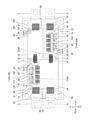
- FIG. 2 is a top view showing the semiconductor device according to the first embodiment.
- FIG. 3 is a cross-sectional view showing the relationship between the heat radiating plate, the first insulating substrate, and the second insulating substrate in the semiconductor device according to the first embodiment.
- FIG. 4 is a cross-sectional view showing the first transistor.
- FIG. 5 is a cross-sectional view showing the first diode.
- FIG. 6 is a cross-sectional view showing the second transistor.
- FIG. 7 is a cross-sectional view showing the second diode.
- FIG. 8 is a circuit diagram showing a semiconductor device according to the first embodiment.
- FIG. 9 is a schematic diagram (No.
- FIG. 10 is a schematic diagram (No. 2) showing the operation of the semiconductor device according to the first embodiment.
- FIG. 11 is a schematic diagram (No. 3) showing the operation of the semiconductor device according to the first embodiment.
- FIG. 12 is a schematic diagram (No. 4) showing the operation of the semiconductor device according to the first embodiment.
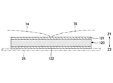
- FIG. 13 is a cross-sectional view showing a modified example of the heat sink.
- FIG. 14 is a schematic diagram showing the configurations of the first insulating substrate and the second insulating substrate in the semiconductor device according to the second embodiment.
- FIG. 15 is a top view showing the semiconductor device according to the third embodiment.
- FIG. 16 is a top view showing the semiconductor device according to the fourth embodiment.
- FIG. 17 is a circuit diagram showing a semiconductor device according to the fourth embodiment.
- An object of the present disclosure is to provide a semiconductor device capable of realizing more stable operation of a plurality of transistors connected in parallel.
- the semiconductor device includes a first insulating substrate, a second insulating substrate, a first arm, a second arm connected to the first arm, and the first insulating substrate. It has a first conductive pattern provided above, the first arm has a plurality of first transistor chips provided on the first insulating substrate, and the second arm has the second insulation. It has a semiconductor chip provided on a substrate, the plurality of first transistor chips are arranged adjacent to each other on the first insulating substrate, and the first electrode of the plurality of first transistors is the first. Directly connected to the conductive pattern, the first electrode is a source electrode or an emitter electrode.
- a plurality of first transistors included in the first arm are arranged next to each other on the first insulating substrate.
- the first electrode is directly connected to the first conductive pattern.
- the semiconductor chip included in the second arm is provided on the second insulating substrate. Therefore, the inductance of each power loop of the plurality of first transistors can be reduced, and the variation of the inductance of the power loop among the plurality of first transistors can be suppressed. Therefore, more stable operation of a plurality of first transistors connected in parallel can be realized.
- the plurality of first transistor chips may be integrated in a rectangular first region. In this case, it is easy to suppress variations in the inductance of the power loop.
- the plurality of first transistor chips may be arranged side by side in the first direction. In this case, it is easy to consolidate a plurality of first transistors to suppress variations in the inductance of the power loop.
- the semiconductor chip may have a second transistor chip.
- the semiconductor device can be operated as an inverter.
- the semiconductor chip has a second conductive pattern provided on the second insulating substrate, and the semiconductor chip has a plurality of second transistor chips, and the plurality of second transistors are included.
- the two transistor chips are arranged next to each other on the second insulating substrate, the second electrodes of the plurality of second transistors are directly connected to the second conductive pattern, and the second electrodes are It may be a source electrode or an emitter electrode. In this case, more stable operation of a plurality of second transistors connected in parallel can be realized.
- the plurality of second transistor chips may be integrated in a rectangular second region. In this case, it is easy to suppress variations in the inductance of the power loop.
- the plurality of second transistor chips may be arranged side by side in the second direction. In this case, it is easy to consolidate a plurality of second transistors to suppress variations in the inductance of the power loop.
- the second arm has a first diode chip connected in parallel to the second transistor chip, and the first diode chip is attached to the first insulating substrate. It may be provided.
- the first diode chip can function as a freewheeling diode with respect to the second transistor chip.
- the first diode chip may be a Schottky barrier diode configured by using silicon carbide. In this case, excellent withstand voltage can be obtained for the first diode chip.
- the second transistor chip may be a field effect transistor configured by using silicon carbide. In this case, excellent withstand voltage can be obtained for the second transistor chip.
- the second control terminal is connected to the second control electrode of the plurality of second transistors, and the second control terminal is more than the first insulating substrate. It may be arranged close to the second insulating substrate. In this case, a plurality of second transistors can be aggregated in the vicinity of the second control terminal. Therefore, it is easy to reduce the difference in the inductance of the gate loop between the plurality of second transistors. Therefore, it is easy to realize more stable operation of a plurality of second transistors connected in parallel.
- the semiconductor chip may have a second diode chip.
- the semiconductor device can be operated as a converter.
- the second diode chip may be a Schottky barrier diode configured by using silicon carbide. In this case, excellent withstand voltage can be obtained for the second diode chip.
- the first arm has a third diode chip connected in parallel to the first transistor chip, and the third diode chip is attached to the second insulating substrate. It may be provided.
- the third diode chip can function as a freewheeling diode with respect to the first transistor chip.
- the third diode chip may be a Schottky barrier diode configured by using silicon carbide. In this case, an excellent withstand voltage can be obtained for the third diode chip.
- the first control terminal is connected to the first control electrode of the plurality of first transistors, and the first control terminal is more than the second insulating substrate. It may be arranged close to the first insulating substrate. In this case, a plurality of first transistors can be aggregated in the vicinity of the first control terminal. Therefore, it is easy to reduce the difference in the inductance of the gate loop among the plurality of first transistors. Therefore, it is easy to realize more stable operation of a plurality of first transistors connected in parallel.
- the first transistor chip may be a field effect transistor configured by using silicon carbide. In this case, excellent withstand voltage can be obtained for the first transistor chip.
- a heat sink having a first main surface and a second main surface opposite to the first main surface is provided, and the first main surface has the first surface. 1 Insulated substrate and the second insulated substrate may be mounted. In this case, the heat generated in the first insulating substrate and the second insulating substrate is likely to be released.
- the second main surface may be curved in a convex shape. In this case, it is easy to obtain good heat transfer efficiency by bringing the heat sink into close contact with the cooler or the like using a thermal interface material or the like.
- FIG. 1 is a perspective view showing a semiconductor device according to the first embodiment.
- FIG. 2 is a top view showing the semiconductor device according to the first embodiment. However, in FIG. 2, the case is seen through.
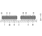
- FIG. 3 is a cross-sectional view showing the relationship between the heat radiating plate, the first insulating substrate, and the second insulating substrate in the semiconductor device according to the first embodiment.
- FIG. 3 corresponds to a cross-sectional view taken along line III-III in FIG.
- the semiconductor device 1 mainly has a heat sink 2, a case 9, a P terminal 3, an N terminal 4, a first O terminal 5, and a second O terminal 6.
- the P terminal 3 is a power supply terminal on the positive electrode side
- the N terminal 4 is a power supply terminal on the negative electrode side
- the first O terminal 5 and the second O terminal 6 are output terminals.
- the P terminal 3, the N terminal 4, the first O terminal 5, and the second O terminal 6 are assembled to the case 9.
- Case 9 further includes a first gate terminal 131, a first sense source terminal 132, a sense drain terminal 133, a second gate terminal 231 and a second sense source terminal 232, and a first thermistor terminal 331.
- the second thermistor terminal 332 is assembled.
- the X1-X2 direction, the Y1-Y2 direction, and the Z1-Z2 direction are defined as directions orthogonal to each other.
- the surface including the X1-X2 direction and the Y1-Y2 direction is defined as the XY surface
- the surface including the Y1-Y2 direction and the Z1-Z2 direction is defined as the YZ surface
- the surface including the Z1-Z2 direction and the X1-X2 direction is defined as the ZX surface. do.
- the Z1 direction is upward and the Z2 direction is downward.
- the plan view means to see the object from the Z1 side.
- the X1-X2 direction is the direction along the long side of the rectangular heat dissipation plate 2 and the case 9 in a plan view
- the Y1-Y2 direction is the direction along the short side of the heat dissipation plate 2 and the case 9, and is the Z1-Z2 direction. Is the direction along the normal line of the heat radiating plate 2 and the case 9.
- the heat radiating plate 2 is, for example, a rectangular body having a uniform thickness in a plan view.
- the heat radiating plate 2 includes a first main surface 2A and a second main surface 2B opposite to the first main surface 2A.
- the material of the heat radiating plate 2 is a metal having high thermal conductivity, for example, copper (Cu), a copper alloy, aluminum (Al), or the like.
- the heat radiating plate 2 is fixed to a cooler or the like using a thermal interface material (TIM) or the like.
- the case 9 is formed in a frame shape in a plan view, for example, and the outer shape of the case 9 is the same as the outer shape of the heat sink 2.
- the material of the case 9 is an insulator such as resin.
- the case 9 has a pair of side wall portions 91 and 92 facing each other, and a pair of end wall portions 93 and 94 connecting both ends of the side wall portions 91 and 92.
- the side wall portions 91 and 92 are arranged parallel to the ZX plane, and the end wall portions 93 and 94 are arranged parallel to the YZ plane.
- the side wall portion 92 is arranged on the Y2 side of the side wall portion 91, and the end wall portion 94 is arranged on the X2 side of the end wall portion 93.
- the case 9 has a terminal block 95 projecting from the end wall portion 93 in the X1 direction, and a terminal block 96 projecting from the end wall portion 94 in the X2 direction.
- the P terminal 3 and the N terminal 4 are arranged on the upper surface (the surface on the Z1 side) of the terminal block 95, and the first O terminal 5 and the second O terminal 6 are arranged on the upper surface (the surface on the Z1 side) of the terminal block 96.
- the N terminal 4 is arranged on the Y2 side of the P terminal 3
- the second O terminal 6 is arranged on the Y2 side of the first O terminal 5.
- the P terminal 3, the N terminal 4, the first O terminal 5, and the second O terminal 6 are made of a metal plate.
- One end of each of the P terminal 3 and the N terminal 4 is exposed on the X2 side of the end wall portion 93, and the other end of each is pulled out to the upper surface of the terminal block 95.
- One end of each of the first O terminal 5 and the second O terminal 6 is exposed on the X1 side of the end wall portion 94, and the other end of each is pulled out to the upper surface of the terminal block 96.
- the first gate terminal 131, the first sense source terminal 132, the sense drain terminal 133, the first thermistor terminal 331, and the second thermistor terminal 332 are attached to the side wall portion 91.
- One end of each of the first gate terminal 131, the first sense source terminal 132, the sense drain terminal 133, the first thermistor terminal 331 and the second thermistor terminal 332 is exposed on the Y2 side of the side wall portion 91, and the other end thereof.
- the end portion of the case 9 protrudes outward (Z1 side) from the upper surface (Z1 side surface) of the side wall portion 91.
- the sense drain terminal 133 is arranged near the end of the side wall portion 91 on the X2 side.
- the first thermistor terminal 331 and the second thermistor terminal 332 are arranged near the end of the side wall portion 91 on the X1 side.
- the second thermistor terminal 332 is arranged on the X1 side of the first thermistor terminal 331.
- the first gate terminal 131 and the first sense source terminal 132 are arranged near the center of the side wall portion 91 in the X1-X2 direction and on the X2 side of the center in the X1-X2 direction.
- the first sense source terminal 132 is arranged on the X2 side of the first gate terminal 131.
- the second gate terminal 231 and the second sense source terminal 232 are attached to the side wall portion 92. One end of each of the second gate terminal 231 and the second sense source terminal 232 is exposed on the Y1 side of the side wall portion 92, and the other end of each is exposed from the upper surface (Z1 side surface) of the side wall portion 92 to the case. It protrudes to the outside (Z1 side) of 9.
- the second gate terminal 231 and the second sense source terminal 232 are arranged near the center of the side wall portion 92 in the X1-X2 direction and on the X1 side of the center in the X1-X2 direction. For example, the second sense source terminal 232 is arranged on the X1 side of the second gate terminal 231.
- the first insulating substrate 10 and the second insulating substrate 20 are arranged on the Z1 side of the heat radiating plate 2. That is, the first insulating substrate 10 and the second insulating substrate 20 are arranged on the first main surface 2A of the heat radiating plate 2. For example, the second insulating substrate 20 is arranged on the X1 side of the first insulating substrate 10.
- the first insulating substrate 10 has conductive layers 11, 12, 13, 14 and 18 on the surface on the Z1 side, and has a conductive layer 19 on the surface on the Z2 side.
- the conductive layer 19 is bonded to the heat radiating plate 2 by a bonding material 7 such as solder.
- a plurality of, for example, four first transistors 110 are mounted on the conductive layer 13.
- the four first transistors 110 are arranged in the X1-X2 direction.
- the first transistor group 110A is composed of four first transistors 110.
- a plurality of, for example, eight second diodes 220 are mounted on the conductive layer 12.
- the eight second diodes 220 are arranged in two rows, four in each of the X1-X2 directions.
- the second diode group 220A is composed of eight second diodes 220.
- the conductive layer 12 is an example of the first conductive pattern.
- the first transistor 110 is an example of a first transistor chip.
- the second diode 220 is an example of a semiconductor chip and a first diode chip.
- the four first transistors 110 are arranged adjacent to each other in the rectangular first transistor aggregation region 110R in a plan view. That is, the four first transistors 110 are aggregated in the first transistor aggregation region 110R.
- the eight second diodes 220 are arranged adjacent to each other in the rectangular second diode aggregation region 220R in a plan view. That is, the eight second diodes 220 are aggregated in the second diode aggregation region 220R.
- the first transistor aggregation region 110R is an example of the first region.
- the second insulating substrate 20 has the conductive layers 21, 22, 23, 24, 25, 26, 27 and 28 on the Z1 side surface and the conductive layer 29 on the Z2 side surface.
- the conductive layer 29 is bonded to the heat radiating plate 2 by a bonding material 8 such as solder.
- a plurality of, for example, four second transistors 210 are mounted on the conductive layer 23.
- the four second transistors 210 are arranged in the X1-X2 direction.
- the second transistor group 210A is composed of four second transistors 210.
- a plurality of, for example, eight first diodes 120 are mounted on the conductive layer 25.
- the eight first diodes 120 are arranged in two rows, four in each of the X1-X2 directions.
- the first diode group 120A is composed of eight first diodes 120.
- the conductive layer 22 is an example of the second conductive pattern.
- the second transistor 210 is an example of a second transistor chip.
- the first diode 120 is an example of a semiconductor chip and a third diode chip.
- the four second transistors 210 are arranged adjacent to each other in the rectangular second transistor aggregation region 210R in a plan view. That is, the four second transistors 210 are aggregated in the second transistor aggregation region 210R.
- the eight first diodes 120 are arranged adjacent to each other in the rectangular first diode aggregation region 120R in a plan view. That is, the eight first diodes 120 are aggregated in the first diode aggregation region 120R.
- the second transistor aggregation region 210R is an example of the second region.
- the X1-X2 direction is also an example of the second direction.
- the first diode aggregation region 120R is separated from the first transistor aggregation region 110R, and the first transistor aggregation region 110R and the first diode aggregation region 120R do not have an overlapping region.
- the first diode 120 is not arranged between the first transistors 110 adjacent to each other.
- the second transistor aggregation region 210R is separated from the second diode aggregation region 220R, and the second transistor aggregation region 210R and the second diode aggregation region 220R do not have an overlapping region.
- the second diode 220 is not arranged between the second transistors 210 adjacent to each other.
- FIG. 4 is a cross-sectional view showing the first transistor.
- FIG. 5 is a cross-sectional view showing the first diode.
- FIG. 6 is a cross-sectional view showing the second transistor.
- FIG. 7 is a cross-sectional view showing the second diode.
- the first transistor 110 has a first gate electrode 111, a first source electrode 112, and a first drain electrode 113.
- the first gate electrode 111 and the first source electrode 112 are arranged on the main surface of the first transistor 110 on the Z1 side, and the first drain electrode 113 is arranged on the main surface of the first transistor 110 on the Z2 side.
- the first drain electrode 113 is bonded to the conductive layer 13 by a bonding material (not shown) such as solder.
- the first source electrode 112 is an example of the first electrode.
- the first diode 120 has a first anode electrode 121 and a first cathode electrode 122.
- the first anode electrode 121 is arranged on the main surface of the first diode 120 on the Z1 side
- the first cathode electrode 122 is arranged on the main surface of the first diode 120 on the Z2 side.
- the first cathode electrode 122 is bonded to the conductive layer 25 by a bonding material (not shown) such as solder.
- the second transistor 210 has a second gate electrode 211, a second source electrode 212, and a second drain electrode 213.
- the second gate electrode 211 and the second source electrode 212 are arranged on the main surface of the second transistor 210 on the Z1 side, and the second drain electrode 213 is arranged on the main surface of the second transistor 210 on the Z2 side.
- the second drain electrode 213 is bonded to the conductive layer 23 by a bonding material (not shown) such as solder.
- the second source electrode 212 is an example of the second electrode.
- the second diode 220 has a second anode electrode 221 and a second cathode electrode 222.
- the second anode electrode 221 is arranged on the main surface of the second diode 220 on the Z1 side
- the second cathode electrode 222 is arranged on the main surface of the second diode 220 on the Z2 side.
- the second cathode electrode 222 is bonded to the conductive layer 12 by a bonding material (not shown) such as solder.
- the semiconductor device 1 has a plurality of wires 31, a plurality of wires 32, a plurality of wires 41, and a plurality of wires 42.
- the wire 31 connects the conductive layer 13 provided on the first insulating substrate 10 and the conductive layer 25 provided on the second insulating substrate 20.
- the wire 32 connects the conductive layer 12 provided on the first insulating substrate 10 and the conductive layer 24 provided on the second insulating substrate 20.
- the wire 41 connects the conductive layer 12 provided on the first insulating substrate 10 and the conductive layer 23 provided on the second insulating substrate 20.
- the wire 42 connects the conductive layer 14 provided on the first insulating substrate 10 and the conductive layer 22 provided on the second insulating substrate 20.
- the semiconductor device 1 has a plurality of wires 51, a plurality of wires 52, a plurality of wires 53, a plurality of wires 54, and a plurality of wires 55.
- the wire 51 connects the first gate electrode 111 provided on each of the four first transistors 110 and the conductive layer 11 provided on the first insulating substrate 10.
- the wire 52 connects the first source electrode 112 provided on each of the four first transistors 110 and the conductive layer 12 provided on the first insulating substrate 10.
- the wire 53 connects the first sense source electrode (not shown) provided on each of the four first transistors 110 and the conductive layer 18 provided on the first insulating substrate 10.
- the wire 54 includes a second anode electrode 221 provided on each of the four second diodes 220 arranged on the Y1 side of the eight second diodes 220 and a conductive layer 14 provided on the first insulating substrate 10.
- the wire 55 includes a second anode electrode 221 provided on each of the four second diodes 220 arranged on the Y1 side of the eight second diodes 220 and four second diodes 220 arranged on the Y2 side. The second anode electrode 221 provided in each of the above is connected.
- the semiconductor device 1 has a wire 61, a plurality of wires 62, a plurality of wires 63, a wire 64, and a wire 65.
- the wire 61 connects the conductive layer 11 provided on the first insulating substrate 10 and the first gate terminal 131.
- the wire 62 connects the conductive layer 12 provided on the first insulating substrate 10 and the first O terminal 5.
- the wire 63 connects the conductive layer 12 provided on the first insulating substrate 10 and the second O terminal 6.
- the wire 64 connects the conductive layer 13 provided on the first insulating substrate 10 and the sense drain terminal 133.
- the wire 65 connects the conductive layer 18 provided on the first insulating substrate 10 and the first sense source terminal 132.
- the semiconductor device 1 has a plurality of wires 71, a plurality of wires 72, a plurality of wires 73, a plurality of wires 74, and a plurality of wires 75.
- the wire 71 connects the second gate electrode 211 provided on each of the four second transistors 210 and the conductive layer 21 provided on the second insulating substrate 20.
- the wire 72 connects the second source electrode 212 provided on each of the four second transistors 210 and the conductive layer 22 provided on the second insulating substrate 20.
- the wire 73 connects the second sense source electrode (not shown) provided on each of the four second transistors 210 and the conductive layer 28 provided on the second insulating substrate 20.
- the wire 74 includes a first anode electrode 121 provided on each of the four first diodes 120 arranged on the Y2 side of the eight first diodes 120 and a conductive layer 24 provided on the second insulating substrate 20. To connect.
- the wire 75 includes a first anode electrode 121 provided on each of the four first diodes 120 arranged on the Y2 side of the eight first diodes 120 and four first diodes 120 arranged on the Y1 side.
- the first anode electrode 121 provided in each of the above is connected to the first anode electrode 121.
- the semiconductor device 1 has a wire 81, a plurality of wires 82, a plurality of wires 83, a wire 85, a wire 86, and a wire 87.
- the wire 81 connects the conductive layer 21 provided on the second insulating substrate 20 and the second gate terminal 231.
- the wire 82 connects the conductive layer 22 provided on the second insulating substrate 20 and the N terminal 4.
- the wire 83 connects the conductive layer 25 provided on the second insulating substrate 20 and the P terminal 3.
- the wire 85 connects the conductive layer 28 provided on the second insulating substrate 20 and the second sense source terminal 232.
- the wire 86 connects the conductive layer 26 provided on the second insulating substrate 20 and the first thermistor terminal 331.
- the wire 87 connects the conductive layer 27 provided on the second insulating substrate 20 and the second thermistor terminal 332.
- the semiconductor device 1 has a thermistor 330 connected to the conductive layer 26 and the conductive
- FIG. 8 is a circuit diagram showing a semiconductor device according to the first embodiment.
- the first cathode electrode 122 of the first diode 120 is connected to the P terminal 3 via the wire 83 and the conductive layer 25. Further, the first drain electrode 113 of the first transistor 110 is connected to the P terminal 3 via the wire 83, the conductive layer 25, the wire 31, and the conductive layer 13.
- the conductive layer 12 is connected to the first O terminal 5 via the wire 62, and is connected to the second O terminal 6 via the wire 63.
- the first source electrode 112 of the first transistor 110 is connected to the conductive layer 12 via the wire 52. Further, the first anode electrode 121 of the first diode is connected to the conductive layer 12 via the wire 32, the conductive layer 24, and the wires 74 and 75.
- the first gate electrode 111 of the first transistor 110 is connected to the first gate terminal 131 via the wire 61, the conductive layer 11, and the wire 51.
- the first sense source electrode of the first transistor 110 is connected to the first sense source terminal 132 via the wire 65, the conductive layer 18, and the wire 53.
- the first drain electrode 113 of the first transistor 110 is connected to the sense drain terminal 133 via the wire 64 and the conductive layer 13.
- the first gate electrode 111 is an example of a first control electrode
- the first gate terminal 131 is an example of a first control terminal.
- the second source electrode 212 of the second transistor 210 is connected to the N terminal 4 via the wire 82, the conductive layer 22, and the wire 72. Further, the second anode electrode 221 of the second diode 220 is connected to the N terminal 4 via the wire 82, the conductive layer 22, the wire 42, and the wires 54 and 55.
- the second cathode electrode 222 of the second transistor 210 is connected to the conductive layer 12. Further, the second drain electrode 213 of the second transistor 210 is connected to the conductive layer 12 via the wire 41 and the conductive layer 23.
- the second gate electrode 211 of the second transistor 210 is connected to the second gate terminal 231 via the wire 81, the conductive layer 21, and the wire 71.
- the second sense source electrode of the second transistor 210 is connected to the second sense source terminal 232 via the wire 85, the conductive layer 28, and the wire 73.
- One electrode of the thermistor 330 is connected to the first thermistor terminal 331 via the wire 86 and the conductive layer 26.
- the other electrode of the thermistor 330 is connected to the second thermistor terminal 332 via the wire 87 and the conductive layer 27.
- the second gate electrode 211 is an example of a second control electrode
- the second gate terminal 231 is an example of a second control terminal.
- the first drain electrode 113 of the first transistor 110 and the first cathode electrode 122 of the first diode 120 are commonly connected to the P terminal 3, and the first source electrode 112 and the first anode electrode 121 are connected.
- the second drain electrode 213 of the second transistor 210 and the second cathode electrode 222 of the second diode 220 are commonly connected to the first O terminal 5 and the second O terminal 6, and the second source electrode 212 and the second anode electrode are connected.
- the 221 is commonly connected to the N terminal 4.
- the upper arm 100 includes a first transistor 110 (first transistor group 110A) and a first diode 120 (first diode group 120A).
- the lower arm 200 includes a second transistor 210 (second transistor group 210A) and a second diode 220 (second diode group 220A).
- the upper arm 100 and the lower arm 200 are connected in series between the P terminal 3 and the N terminal 4.
- the upper arm 100 is an example of the first arm, and the lower arm 200 is an example of the second arm.
- a plurality of first transistors 110 included in the upper arm 100 may be provided only on the first insulating substrate 10, and a plurality of first diodes 120 included in the upper arm 100 may be provided only on the second insulating substrate 20. Further, a plurality of second transistors 210 included in the lower arm 200 may be provided only on the second insulating substrate 20, and a plurality of second diodes 220 included in the lower arm 200 may be provided only on the first insulating substrate 10. ..
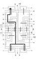
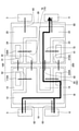
- 9 to 12 are schematic views showing the operation of the semiconductor device according to the first embodiment.
- FIG. 9 shows the path of the current I1 flowing from the P terminal 3 to the first O terminal 5 and the second O terminal 6.
- the current I1 is transferred from the P terminal 3 to the wire 83, the conductive layer 25, the wire 31, the conductive layer 13, the first transistor group 110A, the wire 52, and the conductive layer 12. It flows to the first O terminal 5 and the second O terminal 6 via the wires 62 and 63.
- FIG. 10 shows the path of the current I2 flowing from the first O terminal 5 and the second O terminal 6 to the P terminal 3.
- the current I2 is the first from the first O terminal 5 and the second O terminal 6, the wires 62 and 63, the conductive layer 12, the wire 32, the conductive layer 24, the wires 74 and 75, and the first. It flows to the P terminal 3 via the diode group 120A, the conductive layer 25, and the wire 83.
- the current I1 flowing from the P terminal 3 to the first O terminal 5 and the second O terminal 6 flows through the wire 31, but does not flow through the wire 32.
- the current I2 flowing from the first O terminal 5 and the second O terminal 6 to the P terminal 3 flows through the wire 32, but does not flow through the wire 31.
- FIG. 11 shows the path of the current I3 flowing from the N terminal 4 to the first O terminal 5 and the second O terminal 6.
- the current I3 is, from the N terminal 4, the wire 82, the conductive layer 22, the wire 72, the second transistor group 210A, the conductive layer 23, the wire 41, and the conductive layer 12. It flows to the first O terminal 5 and the second O terminal 6 via the wires 62 and 63.
- FIG. 12 shows the path of the current I4 flowing from the first O terminal 5 and the second O terminal 6 to the N terminal 4.
- the current I4 includes the wires 62 and 63, the conductive layer 12, the second diode group 220A, the wires 54 and 55, and the conductive layer 14 from the first O terminal 5 and the second O terminal 6.
- the wire 42, the conductive layer 22, and the wire 82, and the current flows to the N terminal 4.
- the current I3 flowing from the N terminal 4 to the first O terminal 5 and the second O terminal 6 flows through the wire 41, but does not flow through the wire 42.
- the current I4 flowing from the first O terminal 5 and the second O terminal 6 to the N terminal 4 flows through the wire 42, but does not flow through the wire 41.
- the upper arm 100 includes a first transistor 110 and a first diode 120, the first transistor 110 is provided on the first insulating substrate 10, and the first diode 120 is second insulated. It is provided on the substrate 20. Therefore, the wires 31 and 32 passing between the current I1 flowing from the P terminal 3 to the first O terminal 5 and the second O terminal 6 and the current I2 flowing from the first O terminal 5 and the second O terminal 6 to the P terminal 3 Is different. Therefore, the amount of heat generated in the wires 31 and 32 can be reduced as compared with the case where the current flowing between the first insulating substrate 10 and the second insulating substrate 20 passes through the same connecting member.
- the lower arm 200 includes a second transistor 210 and a second diode 220, the second transistor 210 is provided on the second insulating substrate 20, and the second diode 220 is provided on the first insulating substrate 10. Therefore, the wires 41 and 42 passing between the current I3 flowing from the N terminal 4 to the first O terminal 5 and the second O terminal 6 and the current I4 flowing from the first O terminal 5 and the second O terminal 6 to the N terminal 4 Is different. Therefore, the amount of heat generated in the wires 41 and 42 can be reduced as compared with the case where the current flowing between the first insulating substrate 10 and the second insulating substrate 20 passes through the same connecting member.
- the wires 31, 32, 41 and 42 are used for the connection between the first insulating substrate 10 and the second insulating substrate 20, it is easy to connect the first insulating substrate 10 and the second insulating substrate 20. That is, it is easy to connect the conductive layer 13 and the conductive layer 25, it is easy to connect the conductive layer 12 and the conductive layer 24, it is easy to connect the conductive layer 14 and the conductive layer 22, and the conductive layer 12 and the conductive layer 23 are connected. Easy to connect.
- a metal plate such as a bus bar may be used. In this case, a larger current is likely to flow.
- the wire 52 is used to connect the first source electrode 112 and the conductive layer 12
- the wire 74 is used to connect the first anode electrode 121 and the conductive layer 24
- the first source electrode 112 and the conductive layer 12 are connected. It is easy to connect, and it is easy to connect the first anode electrode 121 and the conductive layer 24.
- the wire 72 is used for connecting the second source electrode 212 and the conductive layer 22
- the wire 54 is used for connecting the second anode electrode 221 and the conductive layer 14, the second source electrode 212 and the conductive layer 22 are connected. Is easy to connect, and it is easy to connect the second anode electrode 221 and the conductive layer 14.
- a plurality of first transistors 110 included in the upper arm 100 are arranged adjacent to each other on the first insulating substrate 10.
- the first source electrode 112 is directly connected to the conductive layer 12. Therefore, the inductance of each power loop of the plurality of first transistors 110 can be reduced, and the variation in the inductance of the power loop among the plurality of first transistors 110 can be suppressed. Therefore, more stable operation of the plurality of first transistors 110 can be realized.
- a plurality of second transistors 210 included in the lower arm 200 are arranged adjacent to each other on the second insulating substrate 20.
- the second source electrode 212 is directly connected to the conductive layer 22. Therefore, the inductance of each power loop of the plurality of second transistors 210 can be reduced, and the variation in the inductance of the power loop among the plurality of second transistors 210 can be suppressed. Therefore, more stable operation of the plurality of second transistors 210 can be realized.
- the first transistor 110 is arranged between the first gate terminal 131 and the second diode 220. That is, the first transistor 110 of the upper arm 100 is arranged closer to the first gate terminal 131 than the second diode 220 of the lower arm 200. Further, a plurality of first transistors 110 can be arranged in the vicinity of the conductive layer 11. Therefore, it is easy to reduce the inductance of the gate loop of the first transistor 110.
- the second transistor 210 is arranged between the second gate terminal 231 and the first diode 120. That is, the second transistor 210 of the lower arm 200 is arranged closer to the second gate terminal 231 than the first diode 120 of the upper arm 100. Further, a plurality of second transistors 210 can be arranged in the vicinity of the conductive layer 21. Therefore, it is easy to reduce the inductance of the gate loop of the second transistor 210.
- first gate electrodes 111 of the plurality of first transistors 110 are connected to the first gate terminal 131, and the plurality of first transistors 110 are arranged between the first gate terminal 131 and the second diode 220. .. Therefore, it is easy to reduce the difference in the inductance of the gate loop among the plurality of first transistors 110.
- second gate electrodes 211 of the plurality of second transistors 210 are connected to the second gate terminal 231, and these plurality of second transistors 210 are arranged between the second gate terminal 231 and the first diode 120. .. Therefore, it is easy to reduce the difference in the inductance of the gate loop among the plurality of second transistors 210.
- the second main surface 2B of the heat sink 2 is curved in a convex shape. This is because it is easy to obtain good heat transfer efficiency by bringing the heat radiating plate 2 into close contact with a cooler or the like using a TIM or the like.
- the first insulating substrate 10 has a third insulating substrate 10A and a fourth insulating substrate 10B, and the second insulating substrate 20 is a fifth. It has an insulating substrate 20A and a sixth insulating substrate 20B.
- the fourth insulated substrate 10B is arranged on the X1 side of the third insulated substrate 10A, and the sixth insulated substrate 20B is arranged on the X2 side of the fifth insulated substrate 20A.
- the third insulating substrate 10A has conductive layers 11A, 12A, 13A, 14A and 18A on the surface on the Z1 side, and has a conductive layer (not shown) on the surface on the Z2 side. Similar to the conductive layer 19, the conductive layer provided on the surface on the Z2 side is bonded to the heat radiating plate 2 by a bonding material 7 such as solder.
- a plurality of, for example, two first transistors 110 are mounted on the conductive layer 13A. The two first transistors 110 are arranged in the X1-X2 direction.
- a plurality of, for example, four second diodes 220 are mounted on the conductive layer 12A. The four second diodes 220 are arranged in two rows, two in each of the X1-X2 directions.
- the fourth insulating substrate 10B has conductive layers 11B, 12B, 12C, 13B, 14B and 18B on the surface on the Z1 side, and has a conductive layer (not shown) on the surface on the Z2 side. Similar to the conductive layer 19, the conductive layer provided on the surface on the Z2 side is bonded to the heat radiating plate 2 by a bonding material 7 such as solder.
- a plurality of, for example, two first transistors 110 are mounted on the conductive layer 13B. The two first transistors 110 are arranged in the X1-X2 direction.
- a plurality of, for example, four second diodes 220 are mounted on the conductive layer 12C. The four second diodes 220 are arranged in two rows, two in each of the X1-X2 directions.
- a wire 411, a wire 412, a wire 413, a wire 414, a wire 415, and a wire 418 are provided.
- the wire 411 connects the conductive layer 11A and the conductive layer 11B.
- the wire 412 connects the conductive layer 12A and the conductive layer 12B.
- the wire 413 connects the conductive layer 13A and the conductive layer 13B.
- the wire 414 connects the conductive layer 14A and the conductive layer 14B.
- the wire 415 connects the conductive layer 12A and the conductive layer 12C.
- the wire 418 connects the conductive layer 18A and the conductive layer 18B.
- the conductive layers 11A and 11B are a part of the conductive layer 11.
- the conductive layers 12A, 12B and 12C are a part of the conductive layer 12.
- the conductive layers 13A and 13B are a part of the conductive layer 13.
- the conductive layers 14A and 14B are a part of the conductive layer 14.
- the conductive layers 18A and 18B are a part of the conductive layer 18.
- the sixth insulating substrate 20B has conductive layers 21B, 22B, 23B, 24B, 25B and 28B on the surface on the Z1 side, and has a conductive layer (not shown) on the surface on the Z2 side. Like the conductive layer 29, the conductive layer provided on the surface on the Z2 side is bonded to the heat radiating plate 2 by a bonding material 8 such as solder.
- a plurality of, for example, two second transistors 210 are mounted on the conductive layer 23B. The two second transistors 210 are arranged in the X1-X2 direction.
- a plurality of, for example, four first diodes 120 are mounted on the conductive layer 25B. The four first diodes 120 are arranged in two rows, two in each of the X1-X2 directions.
- a wire 421, a wire 422, a wire 423, a wire 424, a wire 425, and a wire 428 are provided.
- the wire 421 connects the conductive layer 21A and the conductive layer 21B.
- the wire 422 connects the conductive layer 22A and the conductive layer 22B.
- the wire 423 connects the conductive layer 23A and the conductive layer 23B.
- the wire 424 connects the conductive layer 24A and the conductive layer 24B.
- the wire 425 connects the conductive layer 25A and the conductive layer 25B.
- the wire 428 connects the conductive layer 28A and the conductive layer 28B.
- the conductive layers 21A and 21B are a part of the conductive layer 21.
- the conductive layers 22A and 22B are a part of the conductive layer 22.
- the conductive layers 23A and 23B are a part of the conductive layer 23.
- the conductive layers 24A and 24B are a part of the conductive layer 24.
- the conductive layers 25A and 25B are a part of the conductive layer 25.
- the conductive layers 18A and 18B are a part of the conductive layer 18.
- the second embodiment since the first insulating substrate 10 includes the third insulating substrate 10A and the fourth insulating substrate 10B, the third insulating substrate 10A and the fourth insulating substrate 10B are used as the first main surface 2A of the heat radiating plate 2. It is easier to make close contact.
- the second insulating substrate 20 since the second insulating substrate 20 includes the fifth insulating substrate 20A and the sixth insulating substrate 20B, the fifth insulating substrate 20A and the sixth insulating substrate 20B can be easily brought into close contact with each other by the first main surface 2A of the heat radiating plate 2.
- FIG. 15 is a top view showing the semiconductor device according to the third embodiment. However, as in FIG. 2, in FIG. 15, the case is seen through.
- the semiconductor device according to the third embodiment includes the first diode group 120A, the second diode group 220A, the conductive layers 14 and 24, and the wires 32, 42, 54, 55, 74 and 75. Does not have.
- the upper arm 100 is composed of a plurality of first transistors 110 (first transistor group 110A), and the lower arm 200 is composed of a plurality of second transistors 210 (second transistor group 210A).
- Both the first transistor 110 and the second transistor 210 include a body diode. Therefore, a reflux current can flow through the body diode. The same effect as that of the first embodiment can be obtained by the third embodiment.
- FIG. 16 is a top view showing the semiconductor device according to the fourth embodiment. However, as in FIG. 2, in FIG. 16, the case is seen through.
- the first insulating substrate 10 has the conductive layers 11, 12, 13 and 18 on the surface on the Z1 side, and does not have the conductive layer 14. Similar to the first embodiment, a plurality of, for example, four first transistors 110 are mounted on the conductive layer 13, and a plurality, for example, eight second diodes 220 are mounted on the conductive layer 12. There is.
- the second insulating substrate 20 has conductive layers 22, 24, 25, 26, 27 and 523 on the surface on the Z1 side, and does not have conductive layers 21, 23 and 28.
- a plurality of, for example, eight third diodes 520 are mounted on the conductive layer 523.
- the third diode 520 has the same configuration as, for example, the second diode 220.
- the eight third diodes 520 are arranged in two rows, four in each of the X1-X2 directions.
- a third diode group 520A is composed of eight third diodes 520.
- the eight third diodes 520 are arranged adjacent to each other in the rectangular third diode aggregation region 520R in a plan view. That is, the eight third diodes 520 are aggregated in the third diode aggregation region 520R.
- the third diode 520 is an example of a semiconductor chip and a second diode chip.
- the semiconductor device does not have wires 42, 71, 72, 73, 81 and 85.
- the wire 54 connects the anode electrodes provided on the four third diodes 520 arranged on the Y1 side of the eight third diodes 520 and the conductive layer 22 provided on the second insulating substrate 20. ..
- the wire 55 is provided on each of the anode electrodes provided on the four third diodes 520 arranged on the Y1 side and the four third diodes 520 arranged on the Y2 side among the eight third diodes 520. Connect to the anode electrode.
- the semiconductor device according to the fourth embodiment does not have the second transistor 210, the second diode 220, the second gate terminal 231 and the second sense source terminal 232.
- FIG. 17 is a circuit diagram showing a semiconductor device according to the fourth embodiment.
- the first drain electrode 113 of the first transistor 110 and the first cathode electrode 122 of the first diode 120 are commonly connected to the P terminal 3, and the first source electrode 112 and the first anode electrode 121 are connected. Is commonly connected to the 1st O terminal 5 and the 2nd O terminal 6. That is, the first transistor 110 and the first diode 120 are connected in parallel between the P terminal 3 and the first O terminal 5 and the second O terminal 6. Further, the cathode electrode of the third diode 520 is connected to the first O terminal 5 and the second O terminal 6, and the anode electrode is connected to the N terminal 4. That is, the third diode 520 is connected between the N terminal 4 and the first O terminal 5 and the second O terminal 6.
- the upper arm 100 includes a first transistor 110 (first transistor group 110A) and a first diode 120 (first diode group 120A) as in the first embodiment.
- the lower arm 200 includes the third diode 520 (third diode group 520A), but does not include the second transistor 210 (second transistor group 210A). Similar to the first embodiment, the upper arm 100 and the lower arm 200 are connected in series between the P terminal 3 and the N terminal 4.
- the semiconductor device according to the first to third embodiments can operate as an inverter
- the semiconductor device according to the fourth embodiment can function as a converter
- the fourth embodiment can also realize more stable operation of the plurality of first transistors 110.
- the first diode 120 is connected in parallel to the first transistor 110 to form the upper arm 100, but the first diode 120 may not be included in the upper arm 100.
- the first transistor 110 includes a body diode. Therefore, even if the first diode 120 is not provided, a reflux current can flow through the body diode. In this case as well, the semiconductor device can function as a converter.
- the lower arm 200 includes the second transistor 210 and the second diode 220, the upper arm 100 includes the diode, and the upper arm 100 does not include the transistor. You may. Further, even if the lower arm 200 includes the second transistor 210, the lower arm 200 does not include the second transistor 210, the upper arm 100 contains the diode, and the upper arm 100 does not include the transistor. good. In these cases as well, the semiconductor device can function as a converter.
- the transistor is not limited to the MOS type FET, and the transistor may be an insulated gate bipolar transistor (IGBT).
- IGBT insulated gate bipolar transistor
- the emitter electrode is an example of the first electrode.
Landscapes
- Semiconductor Integrated Circuits (AREA)
- Inverter Devices (AREA)
- Wire Bonding (AREA)
- Cooling Or The Like Of Semiconductors Or Solid State Devices (AREA)
- Chemical & Material Sciences (AREA)
- Engineering & Computer Science (AREA)
- Materials Engineering (AREA)
- Bipolar Transistors (AREA)
- Bipolar Integrated Circuits (AREA)
- Physics & Mathematics (AREA)
- Geometry (AREA)
- Power Conversion In General (AREA)
Priority Applications (3)
| Application Number | Priority Date | Filing Date | Title |
|---|---|---|---|
| US18/043,775 US20230335413A1 (en) | 2020-09-18 | 2021-04-28 | Semiconductor device |
| CN202180051984.4A CN116114052A (zh) | 2020-09-18 | 2021-04-28 | 半导体装置 |
| JP2022550342A JP7619368B2 (ja) | 2020-09-18 | 2021-04-28 | 半導体装置 |
Applications Claiming Priority (2)
| Application Number | Priority Date | Filing Date | Title |
|---|---|---|---|
| JP2020-157444 | 2020-09-18 | ||
| JP2020157444A JP6875588B1 (ja) | 2020-09-18 | 2020-09-18 | 半導体装置 |
Publications (1)
| Publication Number | Publication Date |
|---|---|
| WO2022059251A1 true WO2022059251A1 (ja) | 2022-03-24 |
Family
ID=75961560
Family Applications (3)
| Application Number | Title | Priority Date | Filing Date |
|---|---|---|---|
| PCT/JP2021/017074 Ceased WO2022059251A1 (ja) | 2020-09-18 | 2021-04-28 | 半導体装置 |
| PCT/JP2021/017069 Ceased WO2022059250A1 (ja) | 2020-09-18 | 2021-04-28 | 半導体装置 |
| PCT/JP2021/021824 Ceased WO2022059272A1 (ja) | 2020-09-18 | 2021-06-09 | 半導体装置 |
Family Applications After (2)
| Application Number | Title | Priority Date | Filing Date |
|---|---|---|---|
| PCT/JP2021/017069 Ceased WO2022059250A1 (ja) | 2020-09-18 | 2021-04-28 | 半導体装置 |
| PCT/JP2021/021824 Ceased WO2022059272A1 (ja) | 2020-09-18 | 2021-06-09 | 半導体装置 |
Country Status (4)
| Country | Link |
|---|---|
| US (3) | US20230335413A1 (https=) |
| JP (4) | JP6875588B1 (https=) |
| CN (3) | CN116097439A (https=) |
| WO (3) | WO2022059251A1 (https=) |
Cited By (1)
| Publication number | Priority date | Publication date | Assignee | Title |
|---|---|---|---|---|
| JP2024080323A (ja) * | 2022-12-02 | 2024-06-13 | 三菱電機株式会社 | 半導体装置 |
Families Citing this family (3)
| Publication number | Priority date | Publication date | Assignee | Title |
|---|---|---|---|---|
| JP6875588B1 (ja) * | 2020-09-18 | 2021-05-26 | 住友電気工業株式会社 | 半導体装置 |
| CN117316880A (zh) * | 2023-05-31 | 2023-12-29 | 中国振华集团永光电子有限公司(国营第八七三厂) | 一种igbt模块及其制作工艺 |
| CN117977992B (zh) * | 2024-03-28 | 2025-04-01 | 广州小鹏汽车科技有限公司 | 开关电路、功率集成模块及车辆 |
Citations (8)
| Publication number | Priority date | Publication date | Assignee | Title |
|---|---|---|---|---|
| JP2007088045A (ja) * | 2005-09-20 | 2007-04-05 | Dowa Holdings Co Ltd | 複数の半導体基板を搭載するための放熱板およびそれを用いた半導体基板接合体 |
| WO2013002249A1 (ja) * | 2011-06-27 | 2013-01-03 | ローム株式会社 | 半導体モジュール |
| JP2013118336A (ja) * | 2011-12-05 | 2013-06-13 | Rohm Co Ltd | 半導体装置 |
| JP2015154079A (ja) * | 2014-02-18 | 2015-08-24 | ゼミクロン エレクトローニク ゲーエムベーハー ウント コンパニー カーゲー | 低インダクタンス構成のモジュール内部負荷と補助接続装置を備えるパワー半導体モジュール |
| WO2015136603A1 (ja) * | 2014-03-10 | 2015-09-17 | 株式会社日立製作所 | パワー半導体モジュール及びその製造検査方法 |
| US20170125322A1 (en) * | 2015-10-31 | 2017-05-04 | Ixys Corporation | Bridging DMB Structure for Wire Bonding in a Power Semiconductor Module |
| JP2018532275A (ja) * | 2015-10-29 | 2018-11-01 | アーベーベー・シュバイツ・アーゲー | 半導体モジュール |
| JP6875588B1 (ja) * | 2020-09-18 | 2021-05-26 | 住友電気工業株式会社 | 半導体装置 |
Family Cites Families (11)
| Publication number | Priority date | Publication date | Assignee | Title |
|---|---|---|---|---|
| JP2004095670A (ja) | 2002-08-29 | 2004-03-25 | Toshiba Corp | 半導体装置 |
| JP4988784B2 (ja) | 2009-03-30 | 2012-08-01 | 株式会社日立製作所 | パワー半導体装置 |
| CN109166833B (zh) * | 2010-01-15 | 2022-04-08 | 三菱电机株式会社 | 电力用半导体模块 |
| CN103650137B (zh) * | 2011-07-11 | 2017-09-29 | 三菱电机株式会社 | 功率半导体模块 |
| WO2013171996A1 (ja) * | 2012-05-16 | 2013-11-21 | パナソニック株式会社 | 電力用半導体モジュール |
| JP5791830B2 (ja) | 2012-12-20 | 2015-10-07 | 三菱電機株式会社 | 炭化珪素半導体装置の製造方法 |
| US10263612B2 (en) * | 2013-11-20 | 2019-04-16 | Rohm Co., Ltd. | Switching device and electronic circuit |
| US11094648B2 (en) | 2017-08-04 | 2021-08-17 | Denka Company Limited | Power module |
| CN108807336A (zh) * | 2018-06-06 | 2018-11-13 | 臻驱科技(上海)有限公司 | 一种功率半导体模块衬底及功率半导体模块 |
| JP7116689B2 (ja) | 2019-01-30 | 2022-08-10 | デンカ株式会社 | 放熱部材およびその製造方法 |
| JP7466483B2 (ja) * | 2021-03-17 | 2024-04-12 | 三菱電機株式会社 | 半導体装置 |
-
2020
- 2020-09-18 JP JP2020157444A patent/JP6875588B1/ja active Active
-
2021
- 2021-04-21 JP JP2021071519A patent/JP7543969B2/ja active Active
- 2021-04-28 WO PCT/JP2021/017074 patent/WO2022059251A1/ja not_active Ceased
- 2021-04-28 JP JP2022550341A patent/JP7679838B2/ja active Active
- 2021-04-28 CN CN202180051986.3A patent/CN116097439A/zh active Pending
- 2021-04-28 CN CN202180051984.4A patent/CN116114052A/zh active Pending
- 2021-04-28 JP JP2022550342A patent/JP7619368B2/ja active Active
- 2021-04-28 US US18/043,775 patent/US20230335413A1/en not_active Abandoned
- 2021-04-28 US US18/043,782 patent/US20240021585A1/en active Pending
- 2021-04-28 WO PCT/JP2021/017069 patent/WO2022059250A1/ja not_active Ceased
- 2021-06-09 US US18/043,768 patent/US20230335412A1/en active Pending
- 2021-06-09 WO PCT/JP2021/021824 patent/WO2022059272A1/ja not_active Ceased
- 2021-06-09 CN CN202180051985.9A patent/CN116097430A/zh active Pending
Patent Citations (8)
| Publication number | Priority date | Publication date | Assignee | Title |
|---|---|---|---|---|
| JP2007088045A (ja) * | 2005-09-20 | 2007-04-05 | Dowa Holdings Co Ltd | 複数の半導体基板を搭載するための放熱板およびそれを用いた半導体基板接合体 |
| WO2013002249A1 (ja) * | 2011-06-27 | 2013-01-03 | ローム株式会社 | 半導体モジュール |
| JP2013118336A (ja) * | 2011-12-05 | 2013-06-13 | Rohm Co Ltd | 半導体装置 |
| JP2015154079A (ja) * | 2014-02-18 | 2015-08-24 | ゼミクロン エレクトローニク ゲーエムベーハー ウント コンパニー カーゲー | 低インダクタンス構成のモジュール内部負荷と補助接続装置を備えるパワー半導体モジュール |
| WO2015136603A1 (ja) * | 2014-03-10 | 2015-09-17 | 株式会社日立製作所 | パワー半導体モジュール及びその製造検査方法 |
| JP2018532275A (ja) * | 2015-10-29 | 2018-11-01 | アーベーベー・シュバイツ・アーゲー | 半導体モジュール |
| US20170125322A1 (en) * | 2015-10-31 | 2017-05-04 | Ixys Corporation | Bridging DMB Structure for Wire Bonding in a Power Semiconductor Module |
| JP6875588B1 (ja) * | 2020-09-18 | 2021-05-26 | 住友電気工業株式会社 | 半導体装置 |
Cited By (2)
| Publication number | Priority date | Publication date | Assignee | Title |
|---|---|---|---|---|
| JP2024080323A (ja) * | 2022-12-02 | 2024-06-13 | 三菱電機株式会社 | 半導体装置 |
| JP7840254B2 (ja) | 2022-12-02 | 2026-04-03 | 三菱電機株式会社 | 半導体装置 |
Also Published As
| Publication number | Publication date |
|---|---|
| US20240021585A1 (en) | 2024-01-18 |
| JPWO2022059251A1 (https=) | 2022-03-24 |
| JP2022051135A (ja) | 2022-03-31 |
| JP2022051499A (ja) | 2022-03-31 |
| JP7619368B2 (ja) | 2025-01-22 |
| CN116097430A (zh) | 2023-05-09 |
| US20230335412A1 (en) | 2023-10-19 |
| WO2022059272A1 (ja) | 2022-03-24 |
| CN116097439A (zh) | 2023-05-09 |
| CN116114052A (zh) | 2023-05-12 |
| WO2022059250A1 (ja) | 2022-03-24 |
| US20230335413A1 (en) | 2023-10-19 |
| JP6875588B1 (ja) | 2021-05-26 |
| JP7543969B2 (ja) | 2024-09-03 |
| JP7679838B2 (ja) | 2025-05-20 |
| JPWO2022059250A1 (https=) | 2022-03-24 |
Similar Documents
| Publication | Publication Date | Title |
|---|---|---|
| EP3107120B1 (en) | Power semiconductor module | |
| US11515292B2 (en) | Semiconductor device | |
| JP7428017B2 (ja) | 半導体モジュール | |
| JP7619368B2 (ja) | 半導体装置 | |
| JP7428018B2 (ja) | 半導体モジュール | |
| JP7532813B2 (ja) | 半導体モジュール | |
| US11456244B2 (en) | Semiconductor device | |
| US9159715B2 (en) | Miniaturized semiconductor device | |
| US12033984B2 (en) | Semiconductor device | |
| JP7491043B2 (ja) | 半導体モジュール | |
| JP7484156B2 (ja) | 半導体装置 | |
| CN111613608A (zh) | 用于多芯片功率半导体器件的封装 | |
| CN113287195B (zh) | 半导体装置 | |
| JP7655201B2 (ja) | 半導体装置 | |
| JP2024013924A (ja) | 半導体モジュール | |
| JP7632751B2 (ja) | 半導体モジュール | |
| JP7690863B2 (ja) | 半導体装置 | |
| JP7661796B2 (ja) | 半導体装置 | |
| US20260060119A1 (en) | Semiconductor device | |
| TW200402852A (en) | High power MCM package |
Legal Events
| Date | Code | Title | Description |
|---|---|---|---|
| 121 | Ep: the epo has been informed by wipo that ep was designated in this application |
Ref document number: 21868938 Country of ref document: EP Kind code of ref document: A1 |
|
| ENP | Entry into the national phase |
Ref document number: 2022550342 Country of ref document: JP Kind code of ref document: A |
|
| NENP | Non-entry into the national phase |
Ref country code: DE |
|
| 122 | Ep: pct application non-entry in european phase |
Ref document number: 21868938 Country of ref document: EP Kind code of ref document: A1 |