WO2022059251A1 - Semiconductor device - Google Patents
Semiconductor device Download PDFInfo
- Publication number
- WO2022059251A1 WO2022059251A1 PCT/JP2021/017074 JP2021017074W WO2022059251A1 WO 2022059251 A1 WO2022059251 A1 WO 2022059251A1 JP 2021017074 W JP2021017074 W JP 2021017074W WO 2022059251 A1 WO2022059251 A1 WO 2022059251A1
- Authority
- WO
- WIPO (PCT)
- Prior art keywords
- terminal
- insulating substrate
- transistor
- conductive layer
- semiconductor device
- Prior art date
Links
- 239000004065 semiconductor Substances 0.000 title claims abstract description 87
- 239000000758 substrate Substances 0.000 claims abstract description 141
- HBMJWWWQQXIZIP-UHFFFAOYSA-N silicon carbide Chemical compound [Si+]#[C-] HBMJWWWQQXIZIP-UHFFFAOYSA-N 0.000 claims description 13
- 229910010271 silicon carbide Inorganic materials 0.000 claims description 13
- 230000004888 barrier function Effects 0.000 claims description 7
- 230000005669 field effect Effects 0.000 claims description 6
- 230000002776 aggregation Effects 0.000 description 25
- 238000004220 aggregation Methods 0.000 description 25
- 239000000463 material Substances 0.000 description 15
- 238000010586 diagram Methods 0.000 description 10
- 229910000679 solder Inorganic materials 0.000 description 10
- 230000000694 effects Effects 0.000 description 3
- 229910052751 metal Inorganic materials 0.000 description 3
- 239000002184 metal Substances 0.000 description 3
- 239000010949 copper Substances 0.000 description 2
- 230000017525 heat dissipation Effects 0.000 description 2
- 230000004048 modification Effects 0.000 description 2
- 238000012986 modification Methods 0.000 description 2
- 238000010992 reflux Methods 0.000 description 2
- RYGMFSIKBFXOCR-UHFFFAOYSA-N Copper Chemical compound [Cu] RYGMFSIKBFXOCR-UHFFFAOYSA-N 0.000 description 1
- 229910000881 Cu alloy Inorganic materials 0.000 description 1
- 229910052782 aluminium Inorganic materials 0.000 description 1
- XAGFODPZIPBFFR-UHFFFAOYSA-N aluminium Chemical compound [Al] XAGFODPZIPBFFR-UHFFFAOYSA-N 0.000 description 1
- 229910052802 copper Inorganic materials 0.000 description 1
- 238000009413 insulation Methods 0.000 description 1
- 239000012212 insulator Substances 0.000 description 1
- 239000011347 resin Substances 0.000 description 1
- 229920005989 resin Polymers 0.000 description 1
Images


Classifications
-
- H—ELECTRICITY
- H01—ELECTRIC ELEMENTS
- H01L—SEMICONDUCTOR DEVICES NOT COVERED BY CLASS H10
- H01L23/00—Details of semiconductor or other solid state devices
- H01L23/34—Arrangements for cooling, heating, ventilating or temperature compensation ; Temperature sensing arrangements
- H01L23/36—Selection of materials, or shaping, to facilitate cooling or heating, e.g. heatsinks
- H01L23/373—Cooling facilitated by selection of materials for the device or materials for thermal expansion adaptation, e.g. carbon
- H01L23/3735—Laminates or multilayers, e.g. direct bond copper ceramic substrates
-
- H—ELECTRICITY
- H01—ELECTRIC ELEMENTS
- H01L—SEMICONDUCTOR DEVICES NOT COVERED BY CLASS H10
- H01L21/00—Processes or apparatus adapted for the manufacture or treatment of semiconductor or solid state devices or of parts thereof
- H01L21/02—Manufacture or treatment of semiconductor devices or of parts thereof
- H01L21/04—Manufacture or treatment of semiconductor devices or of parts thereof the devices having at least one potential-jump barrier or surface barrier, e.g. PN junction, depletion layer or carrier concentration layer
- H01L21/50—Assembly of semiconductor devices using processes or apparatus not provided for in a single one of the subgroups H01L21/06 - H01L21/326, e.g. sealing of a cap to a base of a container
- H01L21/60—Attaching or detaching leads or other conductive members, to be used for carrying current to or from the device in operation
-
- H—ELECTRICITY
- H01—ELECTRIC ELEMENTS
- H01L—SEMICONDUCTOR DEVICES NOT COVERED BY CLASS H10
- H01L23/00—Details of semiconductor or other solid state devices
- H01L23/34—Arrangements for cooling, heating, ventilating or temperature compensation ; Temperature sensing arrangements
- H01L23/36—Selection of materials, or shaping, to facilitate cooling or heating, e.g. heatsinks
- H01L23/367—Cooling facilitated by shape of device
- H01L23/3672—Foil-like cooling fins or heat sinks
-
- H—ELECTRICITY
- H01—ELECTRIC ELEMENTS
- H01L—SEMICONDUCTOR DEVICES NOT COVERED BY CLASS H10
- H01L23/00—Details of semiconductor or other solid state devices
- H01L23/52—Arrangements for conducting electric current within the device in operation from one component to another, i.e. interconnections, e.g. wires, lead frames
- H01L23/538—Arrangements for conducting electric current within the device in operation from one component to another, i.e. interconnections, e.g. wires, lead frames the interconnection structure between a plurality of semiconductor chips being formed on, or in, insulating substrates
- H01L23/5385—Assembly of a plurality of insulating substrates
-
- H—ELECTRICITY
- H01—ELECTRIC ELEMENTS
- H01L—SEMICONDUCTOR DEVICES NOT COVERED BY CLASS H10
- H01L24/00—Arrangements for connecting or disconnecting semiconductor or solid-state bodies; Methods or apparatus related thereto
- H01L24/01—Means for bonding being attached to, or being formed on, the surface to be connected, e.g. chip-to-package, die-attach, "first-level" interconnects; Manufacturing methods related thereto
- H01L24/42—Wire connectors; Manufacturing methods related thereto
- H01L24/47—Structure, shape, material or disposition of the wire connectors after the connecting process
- H01L24/48—Structure, shape, material or disposition of the wire connectors after the connecting process of an individual wire connector
-
- H—ELECTRICITY
- H01—ELECTRIC ELEMENTS
- H01L—SEMICONDUCTOR DEVICES NOT COVERED BY CLASS H10
- H01L25/00—Assemblies consisting of a plurality of individual semiconductor or other solid state devices ; Multistep manufacturing processes thereof
- H01L25/03—Assemblies consisting of a plurality of individual semiconductor or other solid state devices ; Multistep manufacturing processes thereof all the devices being of a type provided for in the same subgroup of groups H01L27/00 - H01L33/00, or in a single subclass of H10K, H10N, e.g. assemblies of rectifier diodes
- H01L25/04—Assemblies consisting of a plurality of individual semiconductor or other solid state devices ; Multistep manufacturing processes thereof all the devices being of a type provided for in the same subgroup of groups H01L27/00 - H01L33/00, or in a single subclass of H10K, H10N, e.g. assemblies of rectifier diodes the devices not having separate containers
- H01L25/07—Assemblies consisting of a plurality of individual semiconductor or other solid state devices ; Multistep manufacturing processes thereof all the devices being of a type provided for in the same subgroup of groups H01L27/00 - H01L33/00, or in a single subclass of H10K, H10N, e.g. assemblies of rectifier diodes the devices not having separate containers the devices being of a type provided for in group H01L29/00
- H01L25/072—Assemblies consisting of a plurality of individual semiconductor or other solid state devices ; Multistep manufacturing processes thereof all the devices being of a type provided for in the same subgroup of groups H01L27/00 - H01L33/00, or in a single subclass of H10K, H10N, e.g. assemblies of rectifier diodes the devices not having separate containers the devices being of a type provided for in group H01L29/00 the devices being arranged next to each other
-
- H—ELECTRICITY
- H01—ELECTRIC ELEMENTS
- H01L—SEMICONDUCTOR DEVICES NOT COVERED BY CLASS H10
- H01L25/00—Assemblies consisting of a plurality of individual semiconductor or other solid state devices ; Multistep manufacturing processes thereof
- H01L25/18—Assemblies consisting of a plurality of individual semiconductor or other solid state devices ; Multistep manufacturing processes thereof the devices being of types provided for in two or more different subgroups of the same main group of groups H01L27/00 - H01L33/00, or in a single subclass of H10K, H10N
-
- H—ELECTRICITY
- H01—ELECTRIC ELEMENTS
- H01L—SEMICONDUCTOR DEVICES NOT COVERED BY CLASS H10
- H01L29/00—Semiconductor devices adapted for rectifying, amplifying, oscillating or switching, or capacitors or resistors with at least one potential-jump barrier or surface barrier, e.g. PN junction depletion layer or carrier concentration layer; Details of semiconductor bodies or of electrodes thereof ; Multistep manufacturing processes therefor
- H01L29/02—Semiconductor bodies ; Multistep manufacturing processes therefor
- H01L29/12—Semiconductor bodies ; Multistep manufacturing processes therefor characterised by the materials of which they are formed
- H01L29/16—Semiconductor bodies ; Multistep manufacturing processes therefor characterised by the materials of which they are formed including, apart from doping materials or other impurities, only elements of Group IV of the Periodic System
- H01L29/1608—Silicon carbide
-
- H—ELECTRICITY
- H01—ELECTRIC ELEMENTS
- H01L—SEMICONDUCTOR DEVICES NOT COVERED BY CLASS H10
- H01L29/00—Semiconductor devices adapted for rectifying, amplifying, oscillating or switching, or capacitors or resistors with at least one potential-jump barrier or surface barrier, e.g. PN junction depletion layer or carrier concentration layer; Details of semiconductor bodies or of electrodes thereof ; Multistep manufacturing processes therefor
- H01L29/66—Types of semiconductor device ; Multistep manufacturing processes therefor
- H01L29/86—Types of semiconductor device ; Multistep manufacturing processes therefor controllable only by variation of the electric current supplied, or only the electric potential applied, to one or more of the electrodes carrying the current to be rectified, amplified, oscillated or switched
- H01L29/861—Diodes
- H01L29/872—Schottky diodes
-
- H—ELECTRICITY
- H01—ELECTRIC ELEMENTS
- H01L—SEMICONDUCTOR DEVICES NOT COVERED BY CLASS H10
- H01L2224/00—Indexing scheme for arrangements for connecting or disconnecting semiconductor or solid-state bodies and methods related thereto as covered by H01L24/00
- H01L2224/01—Means for bonding being attached to, or being formed on, the surface to be connected, e.g. chip-to-package, die-attach, "first-level" interconnects; Manufacturing methods related thereto
- H01L2224/02—Bonding areas; Manufacturing methods related thereto
- H01L2224/04—Structure, shape, material or disposition of the bonding areas prior to the connecting process
- H01L2224/06—Structure, shape, material or disposition of the bonding areas prior to the connecting process of a plurality of bonding areas
- H01L2224/0601—Structure
- H01L2224/0603—Bonding areas having different sizes, e.g. different heights or widths
-
- H—ELECTRICITY
- H01—ELECTRIC ELEMENTS
- H01L—SEMICONDUCTOR DEVICES NOT COVERED BY CLASS H10
- H01L2224/00—Indexing scheme for arrangements for connecting or disconnecting semiconductor or solid-state bodies and methods related thereto as covered by H01L24/00
- H01L2224/01—Means for bonding being attached to, or being formed on, the surface to be connected, e.g. chip-to-package, die-attach, "first-level" interconnects; Manufacturing methods related thereto
- H01L2224/42—Wire connectors; Manufacturing methods related thereto
- H01L2224/47—Structure, shape, material or disposition of the wire connectors after the connecting process
- H01L2224/48—Structure, shape, material or disposition of the wire connectors after the connecting process of an individual wire connector
- H01L2224/481—Disposition
- H01L2224/48151—Connecting between a semiconductor or solid-state body and an item not being a semiconductor or solid-state body, e.g. chip-to-substrate, chip-to-passive
- H01L2224/48221—Connecting between a semiconductor or solid-state body and an item not being a semiconductor or solid-state body, e.g. chip-to-substrate, chip-to-passive the body and the item being stacked
- H01L2224/48225—Connecting between a semiconductor or solid-state body and an item not being a semiconductor or solid-state body, e.g. chip-to-substrate, chip-to-passive the body and the item being stacked the item being non-metallic, e.g. insulating substrate with or without metallisation
- H01L2224/48227—Connecting between a semiconductor or solid-state body and an item not being a semiconductor or solid-state body, e.g. chip-to-substrate, chip-to-passive the body and the item being stacked the item being non-metallic, e.g. insulating substrate with or without metallisation connecting the wire to a bond pad of the item
-
- H—ELECTRICITY
- H01—ELECTRIC ELEMENTS
- H01L—SEMICONDUCTOR DEVICES NOT COVERED BY CLASS H10
- H01L2224/00—Indexing scheme for arrangements for connecting or disconnecting semiconductor or solid-state bodies and methods related thereto as covered by H01L24/00
- H01L2224/01—Means for bonding being attached to, or being formed on, the surface to be connected, e.g. chip-to-package, die-attach, "first-level" interconnects; Manufacturing methods related thereto
- H01L2224/42—Wire connectors; Manufacturing methods related thereto
- H01L2224/47—Structure, shape, material or disposition of the wire connectors after the connecting process
- H01L2224/48—Structure, shape, material or disposition of the wire connectors after the connecting process of an individual wire connector
- H01L2224/481—Disposition
- H01L2224/48151—Connecting between a semiconductor or solid-state body and an item not being a semiconductor or solid-state body, e.g. chip-to-substrate, chip-to-passive
- H01L2224/48221—Connecting between a semiconductor or solid-state body and an item not being a semiconductor or solid-state body, e.g. chip-to-substrate, chip-to-passive the body and the item being stacked
- H01L2224/48245—Connecting between a semiconductor or solid-state body and an item not being a semiconductor or solid-state body, e.g. chip-to-substrate, chip-to-passive the body and the item being stacked the item being metallic
- H01L2224/48247—Connecting between a semiconductor or solid-state body and an item not being a semiconductor or solid-state body, e.g. chip-to-substrate, chip-to-passive the body and the item being stacked the item being metallic connecting the wire to a bond pad of the item
-
- H—ELECTRICITY
- H01—ELECTRIC ELEMENTS
- H01L—SEMICONDUCTOR DEVICES NOT COVERED BY CLASS H10
- H01L2224/00—Indexing scheme for arrangements for connecting or disconnecting semiconductor or solid-state bodies and methods related thereto as covered by H01L24/00
- H01L2224/01—Means for bonding being attached to, or being formed on, the surface to be connected, e.g. chip-to-package, die-attach, "first-level" interconnects; Manufacturing methods related thereto
- H01L2224/42—Wire connectors; Manufacturing methods related thereto
- H01L2224/47—Structure, shape, material or disposition of the wire connectors after the connecting process
- H01L2224/49—Structure, shape, material or disposition of the wire connectors after the connecting process of a plurality of wire connectors
- H01L2224/491—Disposition
- H01L2224/4912—Layout
- H01L2224/49175—Parallel arrangements
-
- H—ELECTRICITY
- H01—ELECTRIC ELEMENTS
- H01L—SEMICONDUCTOR DEVICES NOT COVERED BY CLASS H10
- H01L23/00—Details of semiconductor or other solid state devices
- H01L23/52—Arrangements for conducting electric current within the device in operation from one component to another, i.e. interconnections, e.g. wires, lead frames
- H01L23/538—Arrangements for conducting electric current within the device in operation from one component to another, i.e. interconnections, e.g. wires, lead frames the interconnection structure between a plurality of semiconductor chips being formed on, or in, insulating substrates
- H01L23/5386—Geometry or layout of the interconnection structure
-
- H—ELECTRICITY
- H01—ELECTRIC ELEMENTS
- H01L—SEMICONDUCTOR DEVICES NOT COVERED BY CLASS H10
- H01L24/00—Arrangements for connecting or disconnecting semiconductor or solid-state bodies; Methods or apparatus related thereto
- H01L24/01—Means for bonding being attached to, or being formed on, the surface to be connected, e.g. chip-to-package, die-attach, "first-level" interconnects; Manufacturing methods related thereto
- H01L24/42—Wire connectors; Manufacturing methods related thereto
- H01L24/47—Structure, shape, material or disposition of the wire connectors after the connecting process
- H01L24/49—Structure, shape, material or disposition of the wire connectors after the connecting process of a plurality of wire connectors
-
- H—ELECTRICITY
- H01—ELECTRIC ELEMENTS
- H01L—SEMICONDUCTOR DEVICES NOT COVERED BY CLASS H10
- H01L2924/00—Indexing scheme for arrangements or methods for connecting or disconnecting semiconductor or solid-state bodies as covered by H01L24/00
- H01L2924/19—Details of hybrid assemblies other than the semiconductor or other solid state devices to be connected
- H01L2924/191—Disposition
- H01L2924/19101—Disposition of discrete passive components
- H01L2924/19107—Disposition of discrete passive components off-chip wires
Definitions
- This disclosure relates to semiconductor devices.
- the semiconductor device of the present disclosure includes a first insulating substrate, a second insulating substrate, a first arm, a second arm connected to the first arm, and a first insulating substrate provided on the first insulating substrate.
- the first arm has a plurality of first transistor chips provided on the first insulating substrate
- the second arm has a semiconductor chip provided on the second insulating substrate.
- the plurality of first transistor chips are arranged adjacent to each other on the first insulating substrate, and the first electrodes of the plurality of first transistors are directly connected to the first conductive pattern.
- the first electrode is a source electrode or an emitter electrode.
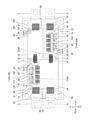
- FIG. 1 is a perspective view showing a semiconductor device according to the first embodiment.
- FIG. 2 is a top view showing the semiconductor device according to the first embodiment.
- FIG. 3 is a cross-sectional view showing the relationship between the heat radiating plate, the first insulating substrate, and the second insulating substrate in the semiconductor device according to the first embodiment.
- FIG. 4 is a cross-sectional view showing the first transistor.
- FIG. 5 is a cross-sectional view showing the first diode.
- FIG. 6 is a cross-sectional view showing the second transistor.
- FIG. 7 is a cross-sectional view showing the second diode.
- FIG. 8 is a circuit diagram showing a semiconductor device according to the first embodiment.
- FIG. 9 is a schematic diagram (No.
- FIG. 10 is a schematic diagram (No. 2) showing the operation of the semiconductor device according to the first embodiment.
- FIG. 11 is a schematic diagram (No. 3) showing the operation of the semiconductor device according to the first embodiment.
- FIG. 12 is a schematic diagram (No. 4) showing the operation of the semiconductor device according to the first embodiment.
- FIG. 13 is a cross-sectional view showing a modified example of the heat sink.
- FIG. 14 is a schematic diagram showing the configurations of the first insulating substrate and the second insulating substrate in the semiconductor device according to the second embodiment.
- FIG. 15 is a top view showing the semiconductor device according to the third embodiment.
- FIG. 16 is a top view showing the semiconductor device according to the fourth embodiment.
- FIG. 17 is a circuit diagram showing a semiconductor device according to the fourth embodiment.
- An object of the present disclosure is to provide a semiconductor device capable of realizing more stable operation of a plurality of transistors connected in parallel.
- the semiconductor device includes a first insulating substrate, a second insulating substrate, a first arm, a second arm connected to the first arm, and the first insulating substrate. It has a first conductive pattern provided above, the first arm has a plurality of first transistor chips provided on the first insulating substrate, and the second arm has the second insulation. It has a semiconductor chip provided on a substrate, the plurality of first transistor chips are arranged adjacent to each other on the first insulating substrate, and the first electrode of the plurality of first transistors is the first. Directly connected to the conductive pattern, the first electrode is a source electrode or an emitter electrode.
- a plurality of first transistors included in the first arm are arranged next to each other on the first insulating substrate.
- the first electrode is directly connected to the first conductive pattern.
- the semiconductor chip included in the second arm is provided on the second insulating substrate. Therefore, the inductance of each power loop of the plurality of first transistors can be reduced, and the variation of the inductance of the power loop among the plurality of first transistors can be suppressed. Therefore, more stable operation of a plurality of first transistors connected in parallel can be realized.
- the plurality of first transistor chips may be integrated in a rectangular first region. In this case, it is easy to suppress variations in the inductance of the power loop.
- the plurality of first transistor chips may be arranged side by side in the first direction. In this case, it is easy to consolidate a plurality of first transistors to suppress variations in the inductance of the power loop.
- the semiconductor chip may have a second transistor chip.
- the semiconductor device can be operated as an inverter.
- the semiconductor chip has a second conductive pattern provided on the second insulating substrate, and the semiconductor chip has a plurality of second transistor chips, and the plurality of second transistors are included.
- the two transistor chips are arranged next to each other on the second insulating substrate, the second electrodes of the plurality of second transistors are directly connected to the second conductive pattern, and the second electrodes are It may be a source electrode or an emitter electrode. In this case, more stable operation of a plurality of second transistors connected in parallel can be realized.
- the plurality of second transistor chips may be integrated in a rectangular second region. In this case, it is easy to suppress variations in the inductance of the power loop.
- the plurality of second transistor chips may be arranged side by side in the second direction. In this case, it is easy to consolidate a plurality of second transistors to suppress variations in the inductance of the power loop.
- the second arm has a first diode chip connected in parallel to the second transistor chip, and the first diode chip is attached to the first insulating substrate. It may be provided.
- the first diode chip can function as a freewheeling diode with respect to the second transistor chip.
- the first diode chip may be a Schottky barrier diode configured by using silicon carbide. In this case, excellent withstand voltage can be obtained for the first diode chip.
- the second transistor chip may be a field effect transistor configured by using silicon carbide. In this case, excellent withstand voltage can be obtained for the second transistor chip.
- the second control terminal is connected to the second control electrode of the plurality of second transistors, and the second control terminal is more than the first insulating substrate. It may be arranged close to the second insulating substrate. In this case, a plurality of second transistors can be aggregated in the vicinity of the second control terminal. Therefore, it is easy to reduce the difference in the inductance of the gate loop between the plurality of second transistors. Therefore, it is easy to realize more stable operation of a plurality of second transistors connected in parallel.
- the semiconductor chip may have a second diode chip.
- the semiconductor device can be operated as a converter.
- the second diode chip may be a Schottky barrier diode configured by using silicon carbide. In this case, excellent withstand voltage can be obtained for the second diode chip.
- the first arm has a third diode chip connected in parallel to the first transistor chip, and the third diode chip is attached to the second insulating substrate. It may be provided.
- the third diode chip can function as a freewheeling diode with respect to the first transistor chip.
- the third diode chip may be a Schottky barrier diode configured by using silicon carbide. In this case, an excellent withstand voltage can be obtained for the third diode chip.
- the first control terminal is connected to the first control electrode of the plurality of first transistors, and the first control terminal is more than the second insulating substrate. It may be arranged close to the first insulating substrate. In this case, a plurality of first transistors can be aggregated in the vicinity of the first control terminal. Therefore, it is easy to reduce the difference in the inductance of the gate loop among the plurality of first transistors. Therefore, it is easy to realize more stable operation of a plurality of first transistors connected in parallel.
- the first transistor chip may be a field effect transistor configured by using silicon carbide. In this case, excellent withstand voltage can be obtained for the first transistor chip.
- a heat sink having a first main surface and a second main surface opposite to the first main surface is provided, and the first main surface has the first surface. 1 Insulated substrate and the second insulated substrate may be mounted. In this case, the heat generated in the first insulating substrate and the second insulating substrate is likely to be released.
- the second main surface may be curved in a convex shape. In this case, it is easy to obtain good heat transfer efficiency by bringing the heat sink into close contact with the cooler or the like using a thermal interface material or the like.
- FIG. 1 is a perspective view showing a semiconductor device according to the first embodiment.
- FIG. 2 is a top view showing the semiconductor device according to the first embodiment. However, in FIG. 2, the case is seen through.
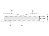
- FIG. 3 is a cross-sectional view showing the relationship between the heat radiating plate, the first insulating substrate, and the second insulating substrate in the semiconductor device according to the first embodiment.
- FIG. 3 corresponds to a cross-sectional view taken along line III-III in FIG.
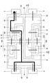
- the semiconductor device 1 mainly has a heat sink 2, a case 9, a P terminal 3, an N terminal 4, a first O terminal 5, and a second O terminal 6.
- the P terminal 3 is a power supply terminal on the positive electrode side
- the N terminal 4 is a power supply terminal on the negative electrode side
- the first O terminal 5 and the second O terminal 6 are output terminals.
- the P terminal 3, the N terminal 4, the first O terminal 5, and the second O terminal 6 are assembled to the case 9.
- Case 9 further includes a first gate terminal 131, a first sense source terminal 132, a sense drain terminal 133, a second gate terminal 231 and a second sense source terminal 232, and a first thermistor terminal 331.
- the second thermistor terminal 332 is assembled.
- the X1-X2 direction, the Y1-Y2 direction, and the Z1-Z2 direction are defined as directions orthogonal to each other.
- the surface including the X1-X2 direction and the Y1-Y2 direction is defined as the XY surface
- the surface including the Y1-Y2 direction and the Z1-Z2 direction is defined as the YZ surface
- the surface including the Z1-Z2 direction and the X1-X2 direction is defined as the ZX surface. do.
- the Z1 direction is upward and the Z2 direction is downward.
- the plan view means to see the object from the Z1 side.
- the X1-X2 direction is the direction along the long side of the rectangular heat dissipation plate 2 and the case 9 in a plan view
- the Y1-Y2 direction is the direction along the short side of the heat dissipation plate 2 and the case 9, and is the Z1-Z2 direction. Is the direction along the normal line of the heat radiating plate 2 and the case 9.
- the heat radiating plate 2 is, for example, a rectangular body having a uniform thickness in a plan view.
- the heat radiating plate 2 includes a first main surface 2A and a second main surface 2B opposite to the first main surface 2A.
- the material of the heat radiating plate 2 is a metal having high thermal conductivity, for example, copper (Cu), a copper alloy, aluminum (Al), or the like.
- the heat radiating plate 2 is fixed to a cooler or the like using a thermal interface material (TIM) or the like.
- the case 9 is formed in a frame shape in a plan view, for example, and the outer shape of the case 9 is the same as the outer shape of the heat sink 2.
- the material of the case 9 is an insulator such as resin.
- the case 9 has a pair of side wall portions 91 and 92 facing each other, and a pair of end wall portions 93 and 94 connecting both ends of the side wall portions 91 and 92.
- the side wall portions 91 and 92 are arranged parallel to the ZX plane, and the end wall portions 93 and 94 are arranged parallel to the YZ plane.
- the side wall portion 92 is arranged on the Y2 side of the side wall portion 91, and the end wall portion 94 is arranged on the X2 side of the end wall portion 93.
- the case 9 has a terminal block 95 projecting from the end wall portion 93 in the X1 direction, and a terminal block 96 projecting from the end wall portion 94 in the X2 direction.
- the P terminal 3 and the N terminal 4 are arranged on the upper surface (the surface on the Z1 side) of the terminal block 95, and the first O terminal 5 and the second O terminal 6 are arranged on the upper surface (the surface on the Z1 side) of the terminal block 96.
- the N terminal 4 is arranged on the Y2 side of the P terminal 3
- the second O terminal 6 is arranged on the Y2 side of the first O terminal 5.
- the P terminal 3, the N terminal 4, the first O terminal 5, and the second O terminal 6 are made of a metal plate.
- One end of each of the P terminal 3 and the N terminal 4 is exposed on the X2 side of the end wall portion 93, and the other end of each is pulled out to the upper surface of the terminal block 95.
- One end of each of the first O terminal 5 and the second O terminal 6 is exposed on the X1 side of the end wall portion 94, and the other end of each is pulled out to the upper surface of the terminal block 96.
- the first gate terminal 131, the first sense source terminal 132, the sense drain terminal 133, the first thermistor terminal 331, and the second thermistor terminal 332 are attached to the side wall portion 91.
- One end of each of the first gate terminal 131, the first sense source terminal 132, the sense drain terminal 133, the first thermistor terminal 331 and the second thermistor terminal 332 is exposed on the Y2 side of the side wall portion 91, and the other end thereof.
- the end portion of the case 9 protrudes outward (Z1 side) from the upper surface (Z1 side surface) of the side wall portion 91.
- the sense drain terminal 133 is arranged near the end of the side wall portion 91 on the X2 side.
- the first thermistor terminal 331 and the second thermistor terminal 332 are arranged near the end of the side wall portion 91 on the X1 side.
- the second thermistor terminal 332 is arranged on the X1 side of the first thermistor terminal 331.
- the first gate terminal 131 and the first sense source terminal 132 are arranged near the center of the side wall portion 91 in the X1-X2 direction and on the X2 side of the center in the X1-X2 direction.
- the first sense source terminal 132 is arranged on the X2 side of the first gate terminal 131.
- the second gate terminal 231 and the second sense source terminal 232 are attached to the side wall portion 92. One end of each of the second gate terminal 231 and the second sense source terminal 232 is exposed on the Y1 side of the side wall portion 92, and the other end of each is exposed from the upper surface (Z1 side surface) of the side wall portion 92 to the case. It protrudes to the outside (Z1 side) of 9.
- the second gate terminal 231 and the second sense source terminal 232 are arranged near the center of the side wall portion 92 in the X1-X2 direction and on the X1 side of the center in the X1-X2 direction. For example, the second sense source terminal 232 is arranged on the X1 side of the second gate terminal 231.
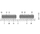
- the first insulating substrate 10 and the second insulating substrate 20 are arranged on the Z1 side of the heat radiating plate 2. That is, the first insulating substrate 10 and the second insulating substrate 20 are arranged on the first main surface 2A of the heat radiating plate 2. For example, the second insulating substrate 20 is arranged on the X1 side of the first insulating substrate 10.
- the first insulating substrate 10 has conductive layers 11, 12, 13, 14 and 18 on the surface on the Z1 side, and has a conductive layer 19 on the surface on the Z2 side.
- the conductive layer 19 is bonded to the heat radiating plate 2 by a bonding material 7 such as solder.
- a plurality of, for example, four first transistors 110 are mounted on the conductive layer 13.
- the four first transistors 110 are arranged in the X1-X2 direction.
- the first transistor group 110A is composed of four first transistors 110.
- a plurality of, for example, eight second diodes 220 are mounted on the conductive layer 12.
- the eight second diodes 220 are arranged in two rows, four in each of the X1-X2 directions.
- the second diode group 220A is composed of eight second diodes 220.
- the conductive layer 12 is an example of the first conductive pattern.
- the first transistor 110 is an example of a first transistor chip.
- the second diode 220 is an example of a semiconductor chip and a first diode chip.
- the four first transistors 110 are arranged adjacent to each other in the rectangular first transistor aggregation region 110R in a plan view. That is, the four first transistors 110 are aggregated in the first transistor aggregation region 110R.
- the eight second diodes 220 are arranged adjacent to each other in the rectangular second diode aggregation region 220R in a plan view. That is, the eight second diodes 220 are aggregated in the second diode aggregation region 220R.
- the first transistor aggregation region 110R is an example of the first region.
- the second insulating substrate 20 has the conductive layers 21, 22, 23, 24, 25, 26, 27 and 28 on the Z1 side surface and the conductive layer 29 on the Z2 side surface.
- the conductive layer 29 is bonded to the heat radiating plate 2 by a bonding material 8 such as solder.
- a plurality of, for example, four second transistors 210 are mounted on the conductive layer 23.
- the four second transistors 210 are arranged in the X1-X2 direction.
- the second transistor group 210A is composed of four second transistors 210.
- a plurality of, for example, eight first diodes 120 are mounted on the conductive layer 25.
- the eight first diodes 120 are arranged in two rows, four in each of the X1-X2 directions.
- the first diode group 120A is composed of eight first diodes 120.
- the conductive layer 22 is an example of the second conductive pattern.
- the second transistor 210 is an example of a second transistor chip.
- the first diode 120 is an example of a semiconductor chip and a third diode chip.
- the four second transistors 210 are arranged adjacent to each other in the rectangular second transistor aggregation region 210R in a plan view. That is, the four second transistors 210 are aggregated in the second transistor aggregation region 210R.
- the eight first diodes 120 are arranged adjacent to each other in the rectangular first diode aggregation region 120R in a plan view. That is, the eight first diodes 120 are aggregated in the first diode aggregation region 120R.
- the second transistor aggregation region 210R is an example of the second region.
- the X1-X2 direction is also an example of the second direction.
- the first diode aggregation region 120R is separated from the first transistor aggregation region 110R, and the first transistor aggregation region 110R and the first diode aggregation region 120R do not have an overlapping region.
- the first diode 120 is not arranged between the first transistors 110 adjacent to each other.
- the second transistor aggregation region 210R is separated from the second diode aggregation region 220R, and the second transistor aggregation region 210R and the second diode aggregation region 220R do not have an overlapping region.
- the second diode 220 is not arranged between the second transistors 210 adjacent to each other.
- FIG. 4 is a cross-sectional view showing the first transistor.
- FIG. 5 is a cross-sectional view showing the first diode.
- FIG. 6 is a cross-sectional view showing the second transistor.
- FIG. 7 is a cross-sectional view showing the second diode.
- the first transistor 110 has a first gate electrode 111, a first source electrode 112, and a first drain electrode 113.
- the first gate electrode 111 and the first source electrode 112 are arranged on the main surface of the first transistor 110 on the Z1 side, and the first drain electrode 113 is arranged on the main surface of the first transistor 110 on the Z2 side.
- the first drain electrode 113 is bonded to the conductive layer 13 by a bonding material (not shown) such as solder.
- the first source electrode 112 is an example of the first electrode.
- the first diode 120 has a first anode electrode 121 and a first cathode electrode 122.
- the first anode electrode 121 is arranged on the main surface of the first diode 120 on the Z1 side
- the first cathode electrode 122 is arranged on the main surface of the first diode 120 on the Z2 side.
- the first cathode electrode 122 is bonded to the conductive layer 25 by a bonding material (not shown) such as solder.
- the second transistor 210 has a second gate electrode 211, a second source electrode 212, and a second drain electrode 213.
- the second gate electrode 211 and the second source electrode 212 are arranged on the main surface of the second transistor 210 on the Z1 side, and the second drain electrode 213 is arranged on the main surface of the second transistor 210 on the Z2 side.
- the second drain electrode 213 is bonded to the conductive layer 23 by a bonding material (not shown) such as solder.
- the second source electrode 212 is an example of the second electrode.
- the second diode 220 has a second anode electrode 221 and a second cathode electrode 222.
- the second anode electrode 221 is arranged on the main surface of the second diode 220 on the Z1 side
- the second cathode electrode 222 is arranged on the main surface of the second diode 220 on the Z2 side.
- the second cathode electrode 222 is bonded to the conductive layer 12 by a bonding material (not shown) such as solder.
- the semiconductor device 1 has a plurality of wires 31, a plurality of wires 32, a plurality of wires 41, and a plurality of wires 42.
- the wire 31 connects the conductive layer 13 provided on the first insulating substrate 10 and the conductive layer 25 provided on the second insulating substrate 20.
- the wire 32 connects the conductive layer 12 provided on the first insulating substrate 10 and the conductive layer 24 provided on the second insulating substrate 20.
- the wire 41 connects the conductive layer 12 provided on the first insulating substrate 10 and the conductive layer 23 provided on the second insulating substrate 20.
- the wire 42 connects the conductive layer 14 provided on the first insulating substrate 10 and the conductive layer 22 provided on the second insulating substrate 20.
- the semiconductor device 1 has a plurality of wires 51, a plurality of wires 52, a plurality of wires 53, a plurality of wires 54, and a plurality of wires 55.
- the wire 51 connects the first gate electrode 111 provided on each of the four first transistors 110 and the conductive layer 11 provided on the first insulating substrate 10.
- the wire 52 connects the first source electrode 112 provided on each of the four first transistors 110 and the conductive layer 12 provided on the first insulating substrate 10.
- the wire 53 connects the first sense source electrode (not shown) provided on each of the four first transistors 110 and the conductive layer 18 provided on the first insulating substrate 10.
- the wire 54 includes a second anode electrode 221 provided on each of the four second diodes 220 arranged on the Y1 side of the eight second diodes 220 and a conductive layer 14 provided on the first insulating substrate 10.
- the wire 55 includes a second anode electrode 221 provided on each of the four second diodes 220 arranged on the Y1 side of the eight second diodes 220 and four second diodes 220 arranged on the Y2 side. The second anode electrode 221 provided in each of the above is connected.
- the semiconductor device 1 has a wire 61, a plurality of wires 62, a plurality of wires 63, a wire 64, and a wire 65.
- the wire 61 connects the conductive layer 11 provided on the first insulating substrate 10 and the first gate terminal 131.
- the wire 62 connects the conductive layer 12 provided on the first insulating substrate 10 and the first O terminal 5.
- the wire 63 connects the conductive layer 12 provided on the first insulating substrate 10 and the second O terminal 6.
- the wire 64 connects the conductive layer 13 provided on the first insulating substrate 10 and the sense drain terminal 133.
- the wire 65 connects the conductive layer 18 provided on the first insulating substrate 10 and the first sense source terminal 132.
- the semiconductor device 1 has a plurality of wires 71, a plurality of wires 72, a plurality of wires 73, a plurality of wires 74, and a plurality of wires 75.
- the wire 71 connects the second gate electrode 211 provided on each of the four second transistors 210 and the conductive layer 21 provided on the second insulating substrate 20.
- the wire 72 connects the second source electrode 212 provided on each of the four second transistors 210 and the conductive layer 22 provided on the second insulating substrate 20.
- the wire 73 connects the second sense source electrode (not shown) provided on each of the four second transistors 210 and the conductive layer 28 provided on the second insulating substrate 20.
- the wire 74 includes a first anode electrode 121 provided on each of the four first diodes 120 arranged on the Y2 side of the eight first diodes 120 and a conductive layer 24 provided on the second insulating substrate 20. To connect.
- the wire 75 includes a first anode electrode 121 provided on each of the four first diodes 120 arranged on the Y2 side of the eight first diodes 120 and four first diodes 120 arranged on the Y1 side.
- the first anode electrode 121 provided in each of the above is connected to the first anode electrode 121.
- the semiconductor device 1 has a wire 81, a plurality of wires 82, a plurality of wires 83, a wire 85, a wire 86, and a wire 87.
- the wire 81 connects the conductive layer 21 provided on the second insulating substrate 20 and the second gate terminal 231.
- the wire 82 connects the conductive layer 22 provided on the second insulating substrate 20 and the N terminal 4.
- the wire 83 connects the conductive layer 25 provided on the second insulating substrate 20 and the P terminal 3.
- the wire 85 connects the conductive layer 28 provided on the second insulating substrate 20 and the second sense source terminal 232.
- the wire 86 connects the conductive layer 26 provided on the second insulating substrate 20 and the first thermistor terminal 331.
- the wire 87 connects the conductive layer 27 provided on the second insulating substrate 20 and the second thermistor terminal 332.
- the semiconductor device 1 has a thermistor 330 connected to the conductive layer 26 and the conductive
- FIG. 8 is a circuit diagram showing a semiconductor device according to the first embodiment.
- the first cathode electrode 122 of the first diode 120 is connected to the P terminal 3 via the wire 83 and the conductive layer 25. Further, the first drain electrode 113 of the first transistor 110 is connected to the P terminal 3 via the wire 83, the conductive layer 25, the wire 31, and the conductive layer 13.
- the conductive layer 12 is connected to the first O terminal 5 via the wire 62, and is connected to the second O terminal 6 via the wire 63.
- the first source electrode 112 of the first transistor 110 is connected to the conductive layer 12 via the wire 52. Further, the first anode electrode 121 of the first diode is connected to the conductive layer 12 via the wire 32, the conductive layer 24, and the wires 74 and 75.
- the first gate electrode 111 of the first transistor 110 is connected to the first gate terminal 131 via the wire 61, the conductive layer 11, and the wire 51.
- the first sense source electrode of the first transistor 110 is connected to the first sense source terminal 132 via the wire 65, the conductive layer 18, and the wire 53.
- the first drain electrode 113 of the first transistor 110 is connected to the sense drain terminal 133 via the wire 64 and the conductive layer 13.
- the first gate electrode 111 is an example of a first control electrode
- the first gate terminal 131 is an example of a first control terminal.
- the second source electrode 212 of the second transistor 210 is connected to the N terminal 4 via the wire 82, the conductive layer 22, and the wire 72. Further, the second anode electrode 221 of the second diode 220 is connected to the N terminal 4 via the wire 82, the conductive layer 22, the wire 42, and the wires 54 and 55.
- the second cathode electrode 222 of the second transistor 210 is connected to the conductive layer 12. Further, the second drain electrode 213 of the second transistor 210 is connected to the conductive layer 12 via the wire 41 and the conductive layer 23.
- the second gate electrode 211 of the second transistor 210 is connected to the second gate terminal 231 via the wire 81, the conductive layer 21, and the wire 71.
- the second sense source electrode of the second transistor 210 is connected to the second sense source terminal 232 via the wire 85, the conductive layer 28, and the wire 73.
- One electrode of the thermistor 330 is connected to the first thermistor terminal 331 via the wire 86 and the conductive layer 26.
- the other electrode of the thermistor 330 is connected to the second thermistor terminal 332 via the wire 87 and the conductive layer 27.
- the second gate electrode 211 is an example of a second control electrode
- the second gate terminal 231 is an example of a second control terminal.
- the first drain electrode 113 of the first transistor 110 and the first cathode electrode 122 of the first diode 120 are commonly connected to the P terminal 3, and the first source electrode 112 and the first anode electrode 121 are connected.
- the second drain electrode 213 of the second transistor 210 and the second cathode electrode 222 of the second diode 220 are commonly connected to the first O terminal 5 and the second O terminal 6, and the second source electrode 212 and the second anode electrode are connected.
- the 221 is commonly connected to the N terminal 4.
- the upper arm 100 includes a first transistor 110 (first transistor group 110A) and a first diode 120 (first diode group 120A).
- the lower arm 200 includes a second transistor 210 (second transistor group 210A) and a second diode 220 (second diode group 220A).
- the upper arm 100 and the lower arm 200 are connected in series between the P terminal 3 and the N terminal 4.
- the upper arm 100 is an example of the first arm, and the lower arm 200 is an example of the second arm.
- a plurality of first transistors 110 included in the upper arm 100 may be provided only on the first insulating substrate 10, and a plurality of first diodes 120 included in the upper arm 100 may be provided only on the second insulating substrate 20. Further, a plurality of second transistors 210 included in the lower arm 200 may be provided only on the second insulating substrate 20, and a plurality of second diodes 220 included in the lower arm 200 may be provided only on the first insulating substrate 10. ..
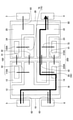
- 9 to 12 are schematic views showing the operation of the semiconductor device according to the first embodiment.
- FIG. 9 shows the path of the current I1 flowing from the P terminal 3 to the first O terminal 5 and the second O terminal 6.
- the current I1 is transferred from the P terminal 3 to the wire 83, the conductive layer 25, the wire 31, the conductive layer 13, the first transistor group 110A, the wire 52, and the conductive layer 12. It flows to the first O terminal 5 and the second O terminal 6 via the wires 62 and 63.
- FIG. 10 shows the path of the current I2 flowing from the first O terminal 5 and the second O terminal 6 to the P terminal 3.
- the current I2 is the first from the first O terminal 5 and the second O terminal 6, the wires 62 and 63, the conductive layer 12, the wire 32, the conductive layer 24, the wires 74 and 75, and the first. It flows to the P terminal 3 via the diode group 120A, the conductive layer 25, and the wire 83.
- the current I1 flowing from the P terminal 3 to the first O terminal 5 and the second O terminal 6 flows through the wire 31, but does not flow through the wire 32.
- the current I2 flowing from the first O terminal 5 and the second O terminal 6 to the P terminal 3 flows through the wire 32, but does not flow through the wire 31.
- FIG. 11 shows the path of the current I3 flowing from the N terminal 4 to the first O terminal 5 and the second O terminal 6.
- the current I3 is, from the N terminal 4, the wire 82, the conductive layer 22, the wire 72, the second transistor group 210A, the conductive layer 23, the wire 41, and the conductive layer 12. It flows to the first O terminal 5 and the second O terminal 6 via the wires 62 and 63.
- FIG. 12 shows the path of the current I4 flowing from the first O terminal 5 and the second O terminal 6 to the N terminal 4.
- the current I4 includes the wires 62 and 63, the conductive layer 12, the second diode group 220A, the wires 54 and 55, and the conductive layer 14 from the first O terminal 5 and the second O terminal 6.
- the wire 42, the conductive layer 22, and the wire 82, and the current flows to the N terminal 4.
- the current I3 flowing from the N terminal 4 to the first O terminal 5 and the second O terminal 6 flows through the wire 41, but does not flow through the wire 42.
- the current I4 flowing from the first O terminal 5 and the second O terminal 6 to the N terminal 4 flows through the wire 42, but does not flow through the wire 41.
- the upper arm 100 includes a first transistor 110 and a first diode 120, the first transistor 110 is provided on the first insulating substrate 10, and the first diode 120 is second insulated. It is provided on the substrate 20. Therefore, the wires 31 and 32 passing between the current I1 flowing from the P terminal 3 to the first O terminal 5 and the second O terminal 6 and the current I2 flowing from the first O terminal 5 and the second O terminal 6 to the P terminal 3 Is different. Therefore, the amount of heat generated in the wires 31 and 32 can be reduced as compared with the case where the current flowing between the first insulating substrate 10 and the second insulating substrate 20 passes through the same connecting member.
- the lower arm 200 includes a second transistor 210 and a second diode 220, the second transistor 210 is provided on the second insulating substrate 20, and the second diode 220 is provided on the first insulating substrate 10. Therefore, the wires 41 and 42 passing between the current I3 flowing from the N terminal 4 to the first O terminal 5 and the second O terminal 6 and the current I4 flowing from the first O terminal 5 and the second O terminal 6 to the N terminal 4 Is different. Therefore, the amount of heat generated in the wires 41 and 42 can be reduced as compared with the case where the current flowing between the first insulating substrate 10 and the second insulating substrate 20 passes through the same connecting member.
- the wires 31, 32, 41 and 42 are used for the connection between the first insulating substrate 10 and the second insulating substrate 20, it is easy to connect the first insulating substrate 10 and the second insulating substrate 20. That is, it is easy to connect the conductive layer 13 and the conductive layer 25, it is easy to connect the conductive layer 12 and the conductive layer 24, it is easy to connect the conductive layer 14 and the conductive layer 22, and the conductive layer 12 and the conductive layer 23 are connected. Easy to connect.
- a metal plate such as a bus bar may be used. In this case, a larger current is likely to flow.
- the wire 52 is used to connect the first source electrode 112 and the conductive layer 12
- the wire 74 is used to connect the first anode electrode 121 and the conductive layer 24
- the first source electrode 112 and the conductive layer 12 are connected. It is easy to connect, and it is easy to connect the first anode electrode 121 and the conductive layer 24.
- the wire 72 is used for connecting the second source electrode 212 and the conductive layer 22
- the wire 54 is used for connecting the second anode electrode 221 and the conductive layer 14, the second source electrode 212 and the conductive layer 22 are connected. Is easy to connect, and it is easy to connect the second anode electrode 221 and the conductive layer 14.
- a plurality of first transistors 110 included in the upper arm 100 are arranged adjacent to each other on the first insulating substrate 10.
- the first source electrode 112 is directly connected to the conductive layer 12. Therefore, the inductance of each power loop of the plurality of first transistors 110 can be reduced, and the variation in the inductance of the power loop among the plurality of first transistors 110 can be suppressed. Therefore, more stable operation of the plurality of first transistors 110 can be realized.
- a plurality of second transistors 210 included in the lower arm 200 are arranged adjacent to each other on the second insulating substrate 20.
- the second source electrode 212 is directly connected to the conductive layer 22. Therefore, the inductance of each power loop of the plurality of second transistors 210 can be reduced, and the variation in the inductance of the power loop among the plurality of second transistors 210 can be suppressed. Therefore, more stable operation of the plurality of second transistors 210 can be realized.
- the first transistor 110 is arranged between the first gate terminal 131 and the second diode 220. That is, the first transistor 110 of the upper arm 100 is arranged closer to the first gate terminal 131 than the second diode 220 of the lower arm 200. Further, a plurality of first transistors 110 can be arranged in the vicinity of the conductive layer 11. Therefore, it is easy to reduce the inductance of the gate loop of the first transistor 110.
- the second transistor 210 is arranged between the second gate terminal 231 and the first diode 120. That is, the second transistor 210 of the lower arm 200 is arranged closer to the second gate terminal 231 than the first diode 120 of the upper arm 100. Further, a plurality of second transistors 210 can be arranged in the vicinity of the conductive layer 21. Therefore, it is easy to reduce the inductance of the gate loop of the second transistor 210.
- first gate electrodes 111 of the plurality of first transistors 110 are connected to the first gate terminal 131, and the plurality of first transistors 110 are arranged between the first gate terminal 131 and the second diode 220. .. Therefore, it is easy to reduce the difference in the inductance of the gate loop among the plurality of first transistors 110.
- second gate electrodes 211 of the plurality of second transistors 210 are connected to the second gate terminal 231, and these plurality of second transistors 210 are arranged between the second gate terminal 231 and the first diode 120. .. Therefore, it is easy to reduce the difference in the inductance of the gate loop among the plurality of second transistors 210.
- the second main surface 2B of the heat sink 2 is curved in a convex shape. This is because it is easy to obtain good heat transfer efficiency by bringing the heat radiating plate 2 into close contact with a cooler or the like using a TIM or the like.
- the first insulating substrate 10 has a third insulating substrate 10A and a fourth insulating substrate 10B, and the second insulating substrate 20 is a fifth. It has an insulating substrate 20A and a sixth insulating substrate 20B.
- the fourth insulated substrate 10B is arranged on the X1 side of the third insulated substrate 10A, and the sixth insulated substrate 20B is arranged on the X2 side of the fifth insulated substrate 20A.
- the third insulating substrate 10A has conductive layers 11A, 12A, 13A, 14A and 18A on the surface on the Z1 side, and has a conductive layer (not shown) on the surface on the Z2 side. Similar to the conductive layer 19, the conductive layer provided on the surface on the Z2 side is bonded to the heat radiating plate 2 by a bonding material 7 such as solder.
- a plurality of, for example, two first transistors 110 are mounted on the conductive layer 13A. The two first transistors 110 are arranged in the X1-X2 direction.
- a plurality of, for example, four second diodes 220 are mounted on the conductive layer 12A. The four second diodes 220 are arranged in two rows, two in each of the X1-X2 directions.
- the fourth insulating substrate 10B has conductive layers 11B, 12B, 12C, 13B, 14B and 18B on the surface on the Z1 side, and has a conductive layer (not shown) on the surface on the Z2 side. Similar to the conductive layer 19, the conductive layer provided on the surface on the Z2 side is bonded to the heat radiating plate 2 by a bonding material 7 such as solder.
- a plurality of, for example, two first transistors 110 are mounted on the conductive layer 13B. The two first transistors 110 are arranged in the X1-X2 direction.
- a plurality of, for example, four second diodes 220 are mounted on the conductive layer 12C. The four second diodes 220 are arranged in two rows, two in each of the X1-X2 directions.
- a wire 411, a wire 412, a wire 413, a wire 414, a wire 415, and a wire 418 are provided.
- the wire 411 connects the conductive layer 11A and the conductive layer 11B.
- the wire 412 connects the conductive layer 12A and the conductive layer 12B.
- the wire 413 connects the conductive layer 13A and the conductive layer 13B.
- the wire 414 connects the conductive layer 14A and the conductive layer 14B.
- the wire 415 connects the conductive layer 12A and the conductive layer 12C.
- the wire 418 connects the conductive layer 18A and the conductive layer 18B.
- the conductive layers 11A and 11B are a part of the conductive layer 11.
- the conductive layers 12A, 12B and 12C are a part of the conductive layer 12.
- the conductive layers 13A and 13B are a part of the conductive layer 13.
- the conductive layers 14A and 14B are a part of the conductive layer 14.
- the conductive layers 18A and 18B are a part of the conductive layer 18.
- the sixth insulating substrate 20B has conductive layers 21B, 22B, 23B, 24B, 25B and 28B on the surface on the Z1 side, and has a conductive layer (not shown) on the surface on the Z2 side. Like the conductive layer 29, the conductive layer provided on the surface on the Z2 side is bonded to the heat radiating plate 2 by a bonding material 8 such as solder.
- a plurality of, for example, two second transistors 210 are mounted on the conductive layer 23B. The two second transistors 210 are arranged in the X1-X2 direction.
- a plurality of, for example, four first diodes 120 are mounted on the conductive layer 25B. The four first diodes 120 are arranged in two rows, two in each of the X1-X2 directions.
- a wire 421, a wire 422, a wire 423, a wire 424, a wire 425, and a wire 428 are provided.
- the wire 421 connects the conductive layer 21A and the conductive layer 21B.
- the wire 422 connects the conductive layer 22A and the conductive layer 22B.
- the wire 423 connects the conductive layer 23A and the conductive layer 23B.
- the wire 424 connects the conductive layer 24A and the conductive layer 24B.
- the wire 425 connects the conductive layer 25A and the conductive layer 25B.
- the wire 428 connects the conductive layer 28A and the conductive layer 28B.
- the conductive layers 21A and 21B are a part of the conductive layer 21.
- the conductive layers 22A and 22B are a part of the conductive layer 22.
- the conductive layers 23A and 23B are a part of the conductive layer 23.
- the conductive layers 24A and 24B are a part of the conductive layer 24.
- the conductive layers 25A and 25B are a part of the conductive layer 25.
- the conductive layers 18A and 18B are a part of the conductive layer 18.
- the second embodiment since the first insulating substrate 10 includes the third insulating substrate 10A and the fourth insulating substrate 10B, the third insulating substrate 10A and the fourth insulating substrate 10B are used as the first main surface 2A of the heat radiating plate 2. It is easier to make close contact.
- the second insulating substrate 20 since the second insulating substrate 20 includes the fifth insulating substrate 20A and the sixth insulating substrate 20B, the fifth insulating substrate 20A and the sixth insulating substrate 20B can be easily brought into close contact with each other by the first main surface 2A of the heat radiating plate 2.
- FIG. 15 is a top view showing the semiconductor device according to the third embodiment. However, as in FIG. 2, in FIG. 15, the case is seen through.
- the semiconductor device according to the third embodiment includes the first diode group 120A, the second diode group 220A, the conductive layers 14 and 24, and the wires 32, 42, 54, 55, 74 and 75. Does not have.
- the upper arm 100 is composed of a plurality of first transistors 110 (first transistor group 110A), and the lower arm 200 is composed of a plurality of second transistors 210 (second transistor group 210A).
- Both the first transistor 110 and the second transistor 210 include a body diode. Therefore, a reflux current can flow through the body diode. The same effect as that of the first embodiment can be obtained by the third embodiment.
- FIG. 16 is a top view showing the semiconductor device according to the fourth embodiment. However, as in FIG. 2, in FIG. 16, the case is seen through.
- the first insulating substrate 10 has the conductive layers 11, 12, 13 and 18 on the surface on the Z1 side, and does not have the conductive layer 14. Similar to the first embodiment, a plurality of, for example, four first transistors 110 are mounted on the conductive layer 13, and a plurality, for example, eight second diodes 220 are mounted on the conductive layer 12. There is.
- the second insulating substrate 20 has conductive layers 22, 24, 25, 26, 27 and 523 on the surface on the Z1 side, and does not have conductive layers 21, 23 and 28.
- a plurality of, for example, eight third diodes 520 are mounted on the conductive layer 523.
- the third diode 520 has the same configuration as, for example, the second diode 220.
- the eight third diodes 520 are arranged in two rows, four in each of the X1-X2 directions.
- a third diode group 520A is composed of eight third diodes 520.
- the eight third diodes 520 are arranged adjacent to each other in the rectangular third diode aggregation region 520R in a plan view. That is, the eight third diodes 520 are aggregated in the third diode aggregation region 520R.
- the third diode 520 is an example of a semiconductor chip and a second diode chip.
- the semiconductor device does not have wires 42, 71, 72, 73, 81 and 85.
- the wire 54 connects the anode electrodes provided on the four third diodes 520 arranged on the Y1 side of the eight third diodes 520 and the conductive layer 22 provided on the second insulating substrate 20. ..
- the wire 55 is provided on each of the anode electrodes provided on the four third diodes 520 arranged on the Y1 side and the four third diodes 520 arranged on the Y2 side among the eight third diodes 520. Connect to the anode electrode.
- the semiconductor device according to the fourth embodiment does not have the second transistor 210, the second diode 220, the second gate terminal 231 and the second sense source terminal 232.
- FIG. 17 is a circuit diagram showing a semiconductor device according to the fourth embodiment.
- the first drain electrode 113 of the first transistor 110 and the first cathode electrode 122 of the first diode 120 are commonly connected to the P terminal 3, and the first source electrode 112 and the first anode electrode 121 are connected. Is commonly connected to the 1st O terminal 5 and the 2nd O terminal 6. That is, the first transistor 110 and the first diode 120 are connected in parallel between the P terminal 3 and the first O terminal 5 and the second O terminal 6. Further, the cathode electrode of the third diode 520 is connected to the first O terminal 5 and the second O terminal 6, and the anode electrode is connected to the N terminal 4. That is, the third diode 520 is connected between the N terminal 4 and the first O terminal 5 and the second O terminal 6.
- the upper arm 100 includes a first transistor 110 (first transistor group 110A) and a first diode 120 (first diode group 120A) as in the first embodiment.
- the lower arm 200 includes the third diode 520 (third diode group 520A), but does not include the second transistor 210 (second transistor group 210A). Similar to the first embodiment, the upper arm 100 and the lower arm 200 are connected in series between the P terminal 3 and the N terminal 4.
- the semiconductor device according to the first to third embodiments can operate as an inverter
- the semiconductor device according to the fourth embodiment can function as a converter
- the fourth embodiment can also realize more stable operation of the plurality of first transistors 110.
- the first diode 120 is connected in parallel to the first transistor 110 to form the upper arm 100, but the first diode 120 may not be included in the upper arm 100.
- the first transistor 110 includes a body diode. Therefore, even if the first diode 120 is not provided, a reflux current can flow through the body diode. In this case as well, the semiconductor device can function as a converter.
- the lower arm 200 includes the second transistor 210 and the second diode 220, the upper arm 100 includes the diode, and the upper arm 100 does not include the transistor. You may. Further, even if the lower arm 200 includes the second transistor 210, the lower arm 200 does not include the second transistor 210, the upper arm 100 contains the diode, and the upper arm 100 does not include the transistor. good. In these cases as well, the semiconductor device can function as a converter.
- the transistor is not limited to the MOS type FET, and the transistor may be an insulated gate bipolar transistor (IGBT).
- IGBT insulated gate bipolar transistor
- the emitter electrode is an example of the first electrode.
Abstract
This semiconductor device includes a first insulating substrate, a second insulating substrate, a first arm, a second arm connected to the first arm, and a first conductive pattern provided on the first insulating substrate, wherein: the first arm has a plurality of first transistor chips provided on the first insulating substrate; the second arm has a semiconductor chip provided on the second insulating substrate; the plurality of first transistor chips are arranged adjacent to each other on the first insulating substrate; first electrodes of the plurality of first transistors are directly connected to the first conductive pattern; and the first electrodes are source electrodes or emitter electrodes.
Description
本開示は、半導体装置に関する。
This disclosure relates to semiconductor devices.
本出願は、2020年9月18日出願の日本出願第2020-157444号に基づく優先権を主張し、前記日本出願に記載された全ての記載内容を援用するものである。
This application claims priority based on Japanese Application No. 2020-157444 filed on September 18, 2020, and incorporates all the contents described in the Japanese application.
パワーモジュールに使用される半導体装置として、トランジスタのソース電極又はエミッタ電極とダイオードのアノード電極とが互いに接続された半導体装置が提案されている。
As a semiconductor device used for a power module, a semiconductor device in which a transistor source electrode or an emitter electrode and a diode anode electrode are connected to each other has been proposed.
本開示の半導体装置は、第1絶縁基板と、第2絶縁基板と、第1アームと、前記第1アームに接続された第2アームと、前記第1絶縁基板の上に設けられた第1導電パターンと、を有し、前記第1アームは、前記第1絶縁基板に設けられた複数の第1トランジスタチップを有し、前記第2アームは、前記第2絶縁基板に設けられた半導体チップを有し、前記複数の第1トランジスタチップは、前記第1絶縁基板の上に互いに隣り合って配置され、前記複数の第1トランジスタの第1電極は、前記第1導電パターンに直接的に接続され、前記第1電極は、ソース電極又はエミッタ電極である。
The semiconductor device of the present disclosure includes a first insulating substrate, a second insulating substrate, a first arm, a second arm connected to the first arm, and a first insulating substrate provided on the first insulating substrate. The first arm has a plurality of first transistor chips provided on the first insulating substrate, and the second arm has a semiconductor chip provided on the second insulating substrate. The plurality of first transistor chips are arranged adjacent to each other on the first insulating substrate, and the first electrodes of the plurality of first transistors are directly connected to the first conductive pattern. The first electrode is a source electrode or an emitter electrode.
[本開示が解決しようとする課題]
並列に接続された複数のトランジスタのより安定した動作の実現が望まれている。 [Problems to be solved by this disclosure]
It is desired to realize more stable operation of a plurality of transistors connected in parallel.
並列に接続された複数のトランジスタのより安定した動作の実現が望まれている。 [Problems to be solved by this disclosure]
It is desired to realize more stable operation of a plurality of transistors connected in parallel.
本開示は、並列に接続された複数のトランジスタのより安定した動作を実現できる半導体装置を提供することを目的とする。
An object of the present disclosure is to provide a semiconductor device capable of realizing more stable operation of a plurality of transistors connected in parallel.
[本開示の効果]
本開示によれば、並列に接続された複数のトランジスタのより安定した動作を実現できる。 [Effect of this disclosure]
According to the present disclosure, more stable operation of a plurality of transistors connected in parallel can be realized.
本開示によれば、並列に接続された複数のトランジスタのより安定した動作を実現できる。 [Effect of this disclosure]
According to the present disclosure, more stable operation of a plurality of transistors connected in parallel can be realized.
実施するための形態について、以下に説明する。
The form for implementation will be explained below.
[本開示の実施形態の説明]
最初に本開示の実施態様を列記して説明する。以下の説明では、同一または対応する要素には同一の符号を付し、それらについて同じ説明は繰り返さない。 [Explanation of Embodiments of the present disclosure]
First, embodiments of the present disclosure will be listed and described. In the following description, the same or corresponding elements are designated by the same reference numerals, and the same description is not repeated for them.
〔1〕 本開示の一態様に係る半導体装置は、第1絶縁基板と、第2絶縁基板と、第1アームと、前記第1アームに接続された第2アームと、前記第1絶縁基板の上に設けられた第1導電パターンと、を有し、前記第1アームは、前記第1絶縁基板に設けられた複数の第1トランジスタチップを有し、前記第2アームは、前記第2絶縁基板に設けられた半導体チップを有し、前記複数の第1トランジスタチップは、前記第1絶縁基板の上に互いに隣り合って配置され、前記複数の第1トランジスタの第1電極は、前記第1導電パターンに直接的に接続され、前記第1電極は、ソース電極又はエミッタ電極である。
[1] The semiconductor device according to one aspect of the present disclosure includes a first insulating substrate, a second insulating substrate, a first arm, a second arm connected to the first arm, and the first insulating substrate. It has a first conductive pattern provided above, the first arm has a plurality of first transistor chips provided on the first insulating substrate, and the second arm has the second insulation. It has a semiconductor chip provided on a substrate, the plurality of first transistor chips are arranged adjacent to each other on the first insulating substrate, and the first electrode of the plurality of first transistors is the first. Directly connected to the conductive pattern, the first electrode is a source electrode or an emitter electrode.
第1アームに含まれる複数の第1トランジスタが第1絶縁基板の上に互いに隣り合って配置されている。第1電極は第1導電パターンに直接的に接続されている。また、第2アームに含まれる半導体チップは、第2絶縁基板に設けられている。このため、複数の第1トランジスタの個々のパワーループのインダクタンスを低減でき、複数の第1トランジスタの間でパワーループのインダクタンスのばらつきを抑制できる。従って、並列に接続された複数の第1トランジスタのより安定した動作を実現できる。
A plurality of first transistors included in the first arm are arranged next to each other on the first insulating substrate. The first electrode is directly connected to the first conductive pattern. Further, the semiconductor chip included in the second arm is provided on the second insulating substrate. Therefore, the inductance of each power loop of the plurality of first transistors can be reduced, and the variation of the inductance of the power loop among the plurality of first transistors can be suppressed. Therefore, more stable operation of a plurality of first transistors connected in parallel can be realized.
〔2〕 〔1〕において、前記複数の第1トランジスタチップは、矩形状の第1領域内に集約されていてもよい。この場合、パワーループのインダクタンスのばらつきを抑制しやすい。
[2] In [1], the plurality of first transistor chips may be integrated in a rectangular first region. In this case, it is easy to suppress variations in the inductance of the power loop.
〔3〕 〔1〕又は〔2〕において、前記複数の第1トランジスタチップは、第1方向に並んで配置されていてもよい。この場合、複数の第1トランジスタを集約してパワーループのインダクタンスのばらつきを抑制しやすい。
[3] In [1] or [2], the plurality of first transistor chips may be arranged side by side in the first direction. In this case, it is easy to consolidate a plurality of first transistors to suppress variations in the inductance of the power loop.
〔4〕 〔1〕~〔3〕において、前記半導体チップは、第2トランジスタチップを有してもよい。この場合、半導体装置をインバータとして動作させられる。
[4] In [1] to [3], the semiconductor chip may have a second transistor chip. In this case, the semiconductor device can be operated as an inverter.
〔5〕 〔1〕~〔3〕において、前記第2絶縁基板の上に設けられた第2導電パターンを有し、前記半導体チップは、複数の第2トランジスタチップを有し、前記複数の第2トランジスタチップは、前記第2絶縁基板の上に互いに隣り合って配置され、前記複数の第2トランジスタの第2電極は、前記第2導電パターンに直接的に接続され、前記第2電極は、ソース電極又はエミッタ電極であってもよい。この場合、並列に接続された複数の第2トランジスタのより安定した動作を実現できる。
[5] In [1] to [3], the semiconductor chip has a second conductive pattern provided on the second insulating substrate, and the semiconductor chip has a plurality of second transistor chips, and the plurality of second transistors are included. The two transistor chips are arranged next to each other on the second insulating substrate, the second electrodes of the plurality of second transistors are directly connected to the second conductive pattern, and the second electrodes are It may be a source electrode or an emitter electrode. In this case, more stable operation of a plurality of second transistors connected in parallel can be realized.
〔6〕 〔5〕において、前記複数の第2トランジスタチップは、矩形状の第2領域内に集約されていてもよい。この場合、パワーループのインダクタンスのばらつきを抑制しやすい。
In [6] and [5], the plurality of second transistor chips may be integrated in a rectangular second region. In this case, it is easy to suppress variations in the inductance of the power loop.
〔7〕 〔5〕又は〔6〕において、前記複数の第2トランジスタチップは、第2方向に並んで配置されていてもよい。この場合、複数の第2トランジスタを集約してパワーループのインダクタンスのばらつきを抑制しやすい。
In [7] [5] or [6], the plurality of second transistor chips may be arranged side by side in the second direction. In this case, it is easy to consolidate a plurality of second transistors to suppress variations in the inductance of the power loop.
〔8〕 〔4〕~〔7〕において、前記第2アームは、前記第2トランジスタチップに並列に接続された第1ダイオードチップを有し、前記第1ダイオードチップは、前記第1絶縁基板に設けられていてもよい。この場合、第1ダイオードチップを第2トランジスタチップに対する還流ダイオードとして機能させられる。
[8] In [4] to [7], the second arm has a first diode chip connected in parallel to the second transistor chip, and the first diode chip is attached to the first insulating substrate. It may be provided. In this case, the first diode chip can function as a freewheeling diode with respect to the second transistor chip.
〔9〕 〔8〕において、前記第1ダイオードチップは、炭化珪素を用いて構成されたショットキーバリアダイオードであってもよい。この場合、第1ダイオードチップに優れた耐圧が得られる。
In [9] and [8], the first diode chip may be a Schottky barrier diode configured by using silicon carbide. In this case, excellent withstand voltage can be obtained for the first diode chip.
〔10〕 〔4〕~〔9〕において、前記第2トランジスタチップは、炭化珪素を用いて構成された電界効果トランジスタであってもよい。この場合、第2トランジスタチップに優れた耐圧が得られる。
[10] In [4] to [9], the second transistor chip may be a field effect transistor configured by using silicon carbide. In this case, excellent withstand voltage can be obtained for the second transistor chip.
〔11〕 〔4〕~〔10〕において、前記複数の第2トランジスタの第2制御電極に接続された第2制御端子を有し、前記第2制御端子は、前記第1絶縁基板よりも前記第2絶縁基板に近く配置されていてもよい。この場合、複数の第2トランジスタを第2制御端子の近傍に集約することができる。従って、複数の第2トランジスタの間でのゲートループのインダクタンスの相違を低減しやすい。このため、並列に接続された複数の第2トランジスタのより安定した動作を実現しやすい。
[11] In [4] to [10], the second control terminal is connected to the second control electrode of the plurality of second transistors, and the second control terminal is more than the first insulating substrate. It may be arranged close to the second insulating substrate. In this case, a plurality of second transistors can be aggregated in the vicinity of the second control terminal. Therefore, it is easy to reduce the difference in the inductance of the gate loop between the plurality of second transistors. Therefore, it is easy to realize more stable operation of a plurality of second transistors connected in parallel.
〔12〕 〔1〕~〔3〕において、前記半導体チップは、第2ダイオードチップを有してもよい。この場合、半導体装置をコンバータとして動作させられる。
[12] In [1] to [3], the semiconductor chip may have a second diode chip. In this case, the semiconductor device can be operated as a converter.
〔13〕 〔12〕において、前記第2ダイオードチップは、炭化珪素を用いて構成されたショットキーバリアダイオードであってもよい。この場合、第2ダイオードチップに優れた耐圧が得られる。
In [13] and [12], the second diode chip may be a Schottky barrier diode configured by using silicon carbide. In this case, excellent withstand voltage can be obtained for the second diode chip.
〔14〕 〔1〕~〔13〕において、前記第1アームは、前記第1トランジスタチップに並列に接続された第3ダイオードチップを有し、前記第3ダイオードチップは、前記第2絶縁基板に設けられていてもよい。この場合、第3ダイオードチップを第1トランジスタチップに対する還流ダイオードとして機能させられる。
[14] In [1] to [13], the first arm has a third diode chip connected in parallel to the first transistor chip, and the third diode chip is attached to the second insulating substrate. It may be provided. In this case, the third diode chip can function as a freewheeling diode with respect to the first transistor chip.
〔15〕 〔14〕において、前記第3ダイオードチップは、炭化珪素を用いて構成されたショットキーバリアダイオードであってもよい。この場合、第3ダイオードチップに優れた耐圧が得られる。
In [15] and [14], the third diode chip may be a Schottky barrier diode configured by using silicon carbide. In this case, an excellent withstand voltage can be obtained for the third diode chip.
〔16〕 〔1〕~〔15〕において、前記複数の第1トランジスタの第1制御電極に接続された第1制御端子を有し、前記第1制御端子は、前記第2絶縁基板よりも前記第1絶縁基板に近く配置されていてもよい。この場合、複数の第1トランジスタを第1制御端子の近傍に集約することができる。従って、複数の第1トランジスタの間でのゲートループのインダクタンスの相違を低減しやすい。このため、並列に接続された複数の第1トランジスタのより安定した動作を実現しやすい。
[16] In [1] to [15], the first control terminal is connected to the first control electrode of the plurality of first transistors, and the first control terminal is more than the second insulating substrate. It may be arranged close to the first insulating substrate. In this case, a plurality of first transistors can be aggregated in the vicinity of the first control terminal. Therefore, it is easy to reduce the difference in the inductance of the gate loop among the plurality of first transistors. Therefore, it is easy to realize more stable operation of a plurality of first transistors connected in parallel.
〔17〕 〔1〕~〔16〕において、前記第1トランジスタチップは、炭化珪素を用いて構成された電界効果トランジスタであってもよい。この場合、第1トランジスタチップに優れた耐圧が得られる。
[17] In [1] to [16], the first transistor chip may be a field effect transistor configured by using silicon carbide. In this case, excellent withstand voltage can be obtained for the first transistor chip.
〔18〕 〔1〕~〔16〕において、第1主面と、前記第1主面とは反対側の第2主面とを備えた放熱板を有し、前記第1主面に前記第1絶縁基板及び前記第2絶縁基板が搭載されていてもよい。この場合、第1絶縁基板及び第2絶縁基板で発生した熱を放出しやすい。
[18] In [1] to [16], a heat sink having a first main surface and a second main surface opposite to the first main surface is provided, and the first main surface has the first surface. 1 Insulated substrate and the second insulated substrate may be mounted. In this case, the heat generated in the first insulating substrate and the second insulating substrate is likely to be released.
〔19〕 〔18〕において、前記第2主面が凸状に湾曲していてもよい。この場合、熱界面材料等を用いて放熱板を冷却器等に密着させ、良好な伝熱効率を得やすい。
In [19] and [18], the second main surface may be curved in a convex shape. In this case, it is easy to obtain good heat transfer efficiency by bringing the heat sink into close contact with the cooler or the like using a thermal interface material or the like.
[本開示の実施形態の詳細]
以下、本開示の実施形態について詳細に説明するが、本実施形態はこれらに限定されるものではない。なお、本明細書及び図面において、実質的に同一の機能構成を有する構成要素については、同一の符号を付することにより重複した説明を省くことがある。 [Details of Embodiments of the present disclosure]
Hereinafter, embodiments of the present disclosure will be described in detail, but the present embodiments are not limited thereto. In the present specification and the drawings, components having substantially the same functional configuration may be designated by the same reference numerals to omit duplicate explanations.
(第1実施形態)
まず、第1実施形態について説明する。図1は、第1実施形態に係る半導体装置を示す斜視図である。図2は、第1実施形態に係る半導体装置を示す上面図である。ただし、図2では、ケースを透視している。図3は、第1実施形態に係る半導体装置における放熱板と、第1絶縁基板と、第2絶縁基板との関係を示す断面図である。図3は、図2中のIII-III線に沿った断面図に相当する。 (First Embodiment)
First, the first embodiment will be described. FIG. 1 is a perspective view showing a semiconductor device according to the first embodiment. FIG. 2 is a top view showing the semiconductor device according to the first embodiment. However, in FIG. 2, the case is seen through. FIG. 3 is a cross-sectional view showing the relationship between the heat radiating plate, the first insulating substrate, and the second insulating substrate in the semiconductor device according to the first embodiment. FIG. 3 corresponds to a cross-sectional view taken along line III-III in FIG.
第1実施形態に係る半導体装置1は、主として、放熱板2と、ケース9と、P端子3と、N端子4と、第1O端子5と、第2O端子6とを有する。P端子3は正極側の電源端子であり、N端子4は負極側の電源端子であり、第1O端子5及び第2O端子6は出力端子である。P端子3、N端子4、第1O端子5及び第2O端子6はケース9に組み付けられている。ケース9には、更に、第1ゲート端子131と、第1センスソース端子132と、センスドレイン端子133と、第2ゲート端子231と、第2センスソース端子232と、第1サーミスタ端子331と、第2サーミスタ端子332とが組み付けられている。
The semiconductor device 1 according to the first embodiment mainly has a heat sink 2, a case 9, a P terminal 3, an N terminal 4, a first O terminal 5, and a second O terminal 6. The P terminal 3 is a power supply terminal on the positive electrode side, the N terminal 4 is a power supply terminal on the negative electrode side, and the first O terminal 5 and the second O terminal 6 are output terminals. The P terminal 3, the N terminal 4, the first O terminal 5, and the second O terminal 6 are assembled to the case 9. Case 9 further includes a first gate terminal 131, a first sense source terminal 132, a sense drain terminal 133, a second gate terminal 231 and a second sense source terminal 232, and a first thermistor terminal 331. The second thermistor terminal 332 is assembled.
本開示において、X1-X2方向、Y1-Y2方向、Z1-Z2方向を相互に直交する方向とする。X1-X2方向及びY1-Y2方向を含む面をXY面とし、Y1-Y2方向及びZ1-Z2方向を含む面をYZ面とし、Z1-Z2方向及びX1-X2方向を含む面をZX面とする。便宜上、Z1方向を上方向、Z2方向を下方向とする。また、本開示において平面視とは、Z1側から対象物を視ることをいう。X1-X2方向は平面視で矩形状の放熱板2及びケース9の長辺に沿う方向であり、Y1-Y2方向は放熱板2及びケース9の短辺に沿う方向であり、Z1-Z2方向は放熱板2及びケース9の法線に沿う方向である。
In the present disclosure, the X1-X2 direction, the Y1-Y2 direction, and the Z1-Z2 direction are defined as directions orthogonal to each other. The surface including the X1-X2 direction and the Y1-Y2 direction is defined as the XY surface, the surface including the Y1-Y2 direction and the Z1-Z2 direction is defined as the YZ surface, and the surface including the Z1-Z2 direction and the X1-X2 direction is defined as the ZX surface. do. For convenience, the Z1 direction is upward and the Z2 direction is downward. Further, in the present disclosure, the plan view means to see the object from the Z1 side. The X1-X2 direction is the direction along the long side of the rectangular heat dissipation plate 2 and the case 9 in a plan view, and the Y1-Y2 direction is the direction along the short side of the heat dissipation plate 2 and the case 9, and is the Z1-Z2 direction. Is the direction along the normal line of the heat radiating plate 2 and the case 9.
放熱板2は、例えば平面視で矩形状の厚さが一様の板状体である。放熱板2は、第1主面2Aと、第1主面2Aとは反対側の第2主面2Bとを備える。放熱板2の材料は、熱伝導率の高い素材である金属、例えば銅(Cu)、銅合金、アルミニウム(Al)等である。放熱板2は、熱界面材料(thermal interface material:TIM)等を用いて冷却器等に固定される。
The heat radiating plate 2 is, for example, a rectangular body having a uniform thickness in a plan view. The heat radiating plate 2 includes a first main surface 2A and a second main surface 2B opposite to the first main surface 2A. The material of the heat radiating plate 2 is a metal having high thermal conductivity, for example, copper (Cu), a copper alloy, aluminum (Al), or the like. The heat radiating plate 2 is fixed to a cooler or the like using a thermal interface material (TIM) or the like.
ケース9は、例えば平面視において枠状に形成されており、ケース9の外形は放熱板2の外形と同等である。ケース9の材料は樹脂等の絶縁体である。ケース9は、互いに対向する一対の側壁部91及び92と、側壁部91及び92の両端をつなぐ一対の端壁部93及び94とを有する。側壁部91及び92はZX平面に平行に配置され、端壁部93及び94はYZ平面に平行に配置されている。側壁部92は側壁部91のY2側に配置され、端壁部94は端壁部93のX2側に配置されている。ケース9は、端壁部93からX1方向に突出する端子台95と、端壁部94からX2方向に突出する端子台96とを有する。
The case 9 is formed in a frame shape in a plan view, for example, and the outer shape of the case 9 is the same as the outer shape of the heat sink 2. The material of the case 9 is an insulator such as resin. The case 9 has a pair of side wall portions 91 and 92 facing each other, and a pair of end wall portions 93 and 94 connecting both ends of the side wall portions 91 and 92. The side wall portions 91 and 92 are arranged parallel to the ZX plane, and the end wall portions 93 and 94 are arranged parallel to the YZ plane. The side wall portion 92 is arranged on the Y2 side of the side wall portion 91, and the end wall portion 94 is arranged on the X2 side of the end wall portion 93. The case 9 has a terminal block 95 projecting from the end wall portion 93 in the X1 direction, and a terminal block 96 projecting from the end wall portion 94 in the X2 direction.
端子台95の上面(Z1側の表面)にP端子3及びN端子4が配置され、端子台96の上面(Z1側の表面)に第1O端子5及び第2O端子6が配置されている。例えば、N端子4がP端子3のY2側に配置され、第2O端子6が第1O端子5のY2側に配置されている。P端子3、N端子4、第1O端子5及び第2O端子6は金属板から構成されている。P端子3及びN端子4のそれぞれの一方の端部が端壁部93のX2側に露出し、それぞれの他方の端部が端子台95の上面に引き出されている。第1O端子5及び第2O端子6のそれぞれの一方の端部が端壁部94のX1側に露出し、それぞれの他方の端部が端子台96の上面に引き出されている。
The P terminal 3 and the N terminal 4 are arranged on the upper surface (the surface on the Z1 side) of the terminal block 95, and the first O terminal 5 and the second O terminal 6 are arranged on the upper surface (the surface on the Z1 side) of the terminal block 96. For example, the N terminal 4 is arranged on the Y2 side of the P terminal 3, and the second O terminal 6 is arranged on the Y2 side of the first O terminal 5. The P terminal 3, the N terminal 4, the first O terminal 5, and the second O terminal 6 are made of a metal plate. One end of each of the P terminal 3 and the N terminal 4 is exposed on the X2 side of the end wall portion 93, and the other end of each is pulled out to the upper surface of the terminal block 95. One end of each of the first O terminal 5 and the second O terminal 6 is exposed on the X1 side of the end wall portion 94, and the other end of each is pulled out to the upper surface of the terminal block 96.
側壁部91に、第1ゲート端子131、第1センスソース端子132、センスドレイン端子133、第1サーミスタ端子331及び第2サーミスタ端子332が取り付けられている。第1ゲート端子131、第1センスソース端子132、センスドレイン端子133、第1サーミスタ端子331及び第2サーミスタ端子332のそれぞれの一方の端部が側壁部91のY2側に露出し、それぞれの他方の端部が側壁部91の上面(Z1側の表面)からケース9の外方(Z1側)に突出している。センスドレイン端子133は、側壁部91のX2側の端部近傍に配置されている。第1サーミスタ端子331及び第2サーミスタ端子332は、側壁部91のX1側の端部近傍に配置されている。例えば、第2サーミスタ端子332は第1サーミスタ端子331のX1側に配置されている。第1ゲート端子131及び第1センスソース端子132は、側壁部91のX1-X2方向の中心の近傍で、かつX1-X2方向の中心よりもX2側に配置されている。例えば、第1センスソース端子132は第1ゲート端子131のX2側に配置されている。
The first gate terminal 131, the first sense source terminal 132, the sense drain terminal 133, the first thermistor terminal 331, and the second thermistor terminal 332 are attached to the side wall portion 91. One end of each of the first gate terminal 131, the first sense source terminal 132, the sense drain terminal 133, the first thermistor terminal 331 and the second thermistor terminal 332 is exposed on the Y2 side of the side wall portion 91, and the other end thereof. The end portion of the case 9 protrudes outward (Z1 side) from the upper surface (Z1 side surface) of the side wall portion 91. The sense drain terminal 133 is arranged near the end of the side wall portion 91 on the X2 side. The first thermistor terminal 331 and the second thermistor terminal 332 are arranged near the end of the side wall portion 91 on the X1 side. For example, the second thermistor terminal 332 is arranged on the X1 side of the first thermistor terminal 331. The first gate terminal 131 and the first sense source terminal 132 are arranged near the center of the side wall portion 91 in the X1-X2 direction and on the X2 side of the center in the X1-X2 direction. For example, the first sense source terminal 132 is arranged on the X2 side of the first gate terminal 131.
側壁部92に、第2ゲート端子231及び第2センスソース端子232が取り付けられている。第2ゲート端子231及び第2センスソース端子232のそれぞれの一方の端部が側壁部92のY1側に露出し、それぞれの他方の端部が側壁部92の上面(Z1側の表面)からケース9の外方(Z1側)に突出している。第2ゲート端子231及び第2センスソース端子232は、側壁部92のX1-X2方向の中心の近傍で、かつX1-X2方向の中心よりもX1側に配置されている。例えば、第2センスソース端子232は第2ゲート端子231のX1側に配置されている。
The second gate terminal 231 and the second sense source terminal 232 are attached to the side wall portion 92. One end of each of the second gate terminal 231 and the second sense source terminal 232 is exposed on the Y1 side of the side wall portion 92, and the other end of each is exposed from the upper surface (Z1 side surface) of the side wall portion 92 to the case. It protrudes to the outside (Z1 side) of 9. The second gate terminal 231 and the second sense source terminal 232 are arranged near the center of the side wall portion 92 in the X1-X2 direction and on the X1 side of the center in the X1-X2 direction. For example, the second sense source terminal 232 is arranged on the X1 side of the second gate terminal 231.
放熱板2のZ1側に、第1絶縁基板10と、第2絶縁基板20とが配置されている。つまり、放熱板2の第1主面2Aに第1絶縁基板10と、第2絶縁基板20とが配置されている。例えば、第2絶縁基板20は第1絶縁基板10のX1側に配置されている。
The first insulating substrate 10 and the second insulating substrate 20 are arranged on the Z1 side of the heat radiating plate 2. That is, the first insulating substrate 10 and the second insulating substrate 20 are arranged on the first main surface 2A of the heat radiating plate 2. For example, the second insulating substrate 20 is arranged on the X1 side of the first insulating substrate 10.
第1絶縁基板10は、Z1側の面に導電層11、12、13、14及び18を有し、Z2側の面に導電層19を有する。導電層19が、はんだ等の接合材7により放熱板2に接合されている。導電層13の上に複数個、例えば4個の第1トランジスタ110が実装されている。4個の第1トランジスタ110はX1-X2方向に並んでいる。4個の第1トランジスタ110から第1トランジスタ群110Aが構成される。導電層12の上に複数個、例えば8個の第2ダイオード220が実装されている。8個の第2ダイオード220は、2列になってX1-X2方向に4個ずつ並んでいる。8個の第2ダイオード220から第2ダイオード群220Aが構成される。導電層12は第1導電パターンの一例である。第1トランジスタ110は第1トランジスタチップの一例である。第2ダイオード220は半導体チップ及び第1ダイオードチップの一例である。
The first insulating substrate 10 has conductive layers 11, 12, 13, 14 and 18 on the surface on the Z1 side, and has a conductive layer 19 on the surface on the Z2 side. The conductive layer 19 is bonded to the heat radiating plate 2 by a bonding material 7 such as solder. A plurality of, for example, four first transistors 110 are mounted on the conductive layer 13. The four first transistors 110 are arranged in the X1-X2 direction. The first transistor group 110A is composed of four first transistors 110. A plurality of, for example, eight second diodes 220 are mounted on the conductive layer 12. The eight second diodes 220 are arranged in two rows, four in each of the X1-X2 directions. The second diode group 220A is composed of eight second diodes 220. The conductive layer 12 is an example of the first conductive pattern. The first transistor 110 is an example of a first transistor chip. The second diode 220 is an example of a semiconductor chip and a first diode chip.
4個の第1トランジスタ110は平面視で矩形状の第1トランジスタ集約領域110R内に互いに隣り合って配置されている。つまり、4個の第1トランジスタ110は第1トランジスタ集約領域110R内に集約されている。8個の第2ダイオード220は平面視で矩形状の第2ダイオード集約領域220R内に互いに隣り合って配置されている。つまり、8個の第2ダイオード220は第2ダイオード集約領域220R内に集約されている。第1トランジスタ集約領域110Rは第1領域の一例である。
The four first transistors 110 are arranged adjacent to each other in the rectangular first transistor aggregation region 110R in a plan view. That is, the four first transistors 110 are aggregated in the first transistor aggregation region 110R. The eight second diodes 220 are arranged adjacent to each other in the rectangular second diode aggregation region 220R in a plan view. That is, the eight second diodes 220 are aggregated in the second diode aggregation region 220R. The first transistor aggregation region 110R is an example of the first region.
第2絶縁基板20は、Z1側の面に導電層21、22、23、24、25、26、27及び28を有し、Z2側の面に導電層29を有する。導電層29が、はんだ等の接合材8により放熱板2に接合されている。導電層23の上に複数個、例えば4個の第2トランジスタ210が実装されている。4個の第2トランジスタ210はX1-X2方向に並んでいる。4個の第2トランジスタ210から第2トランジスタ群210Aが構成される。導電層25の上に複数個、例えば8個の第1ダイオード120が実装されている。8個の第1ダイオード120は、2列になってX1-X2方向に4個ずつ並んでいる。8個の第1ダイオード120から第1ダイオード群120Aが構成される。導電層22は第2導電パターンの一例である。第2トランジスタ210は第2トランジスタチップの一例である。第1ダイオード120は半導体チップ及び第3ダイオードチップの一例である。
The second insulating substrate 20 has the conductive layers 21, 22, 23, 24, 25, 26, 27 and 28 on the Z1 side surface and the conductive layer 29 on the Z2 side surface. The conductive layer 29 is bonded to the heat radiating plate 2 by a bonding material 8 such as solder. A plurality of, for example, four second transistors 210 are mounted on the conductive layer 23. The four second transistors 210 are arranged in the X1-X2 direction. The second transistor group 210A is composed of four second transistors 210. A plurality of, for example, eight first diodes 120 are mounted on the conductive layer 25. The eight first diodes 120 are arranged in two rows, four in each of the X1-X2 directions. The first diode group 120A is composed of eight first diodes 120. The conductive layer 22 is an example of the second conductive pattern. The second transistor 210 is an example of a second transistor chip. The first diode 120 is an example of a semiconductor chip and a third diode chip.
4個の第2トランジスタ210は平面視で矩形状の第2トランジスタ集約領域210R内に互いに隣り合って配置されている。つまり、4個の第2トランジスタ210は第2トランジスタ集約領域210R内に集約されている。8個の第1ダイオード120は平面視で矩形状の第1ダイオード集約領域120R内に互いに隣り合って配置されている。つまり、8個の第1ダイオード120は第1ダイオード集約領域120R内に集約されている。第2トランジスタ集約領域210Rは第2領域の一例である。X1-X2方向は第2方向の一例でもある。
The four second transistors 210 are arranged adjacent to each other in the rectangular second transistor aggregation region 210R in a plan view. That is, the four second transistors 210 are aggregated in the second transistor aggregation region 210R. The eight first diodes 120 are arranged adjacent to each other in the rectangular first diode aggregation region 120R in a plan view. That is, the eight first diodes 120 are aggregated in the first diode aggregation region 120R. The second transistor aggregation region 210R is an example of the second region. The X1-X2 direction is also an example of the second direction.
平面視で、第1ダイオード集約領域120Rは第1トランジスタ集約領域110Rから離れており、第1トランジスタ集約領域110R及び第1ダイオード集約領域120Rは互いに重なる領域を有しない。互いに隣り合う第1トランジスタ110の間には、第1ダイオード120が配置されていない。平面視で、第2トランジスタ集約領域210Rは第2ダイオード集約領域220Rから離れており、第2トランジスタ集約領域210R及び第2ダイオード集約領域220Rは互いに重なる領域を有しない。互いに隣り合う第2トランジスタ210の間には、第2ダイオード220が配置されていない。
In a plan view, the first diode aggregation region 120R is separated from the first transistor aggregation region 110R, and the first transistor aggregation region 110R and the first diode aggregation region 120R do not have an overlapping region. The first diode 120 is not arranged between the first transistors 110 adjacent to each other. In a plan view, the second transistor aggregation region 210R is separated from the second diode aggregation region 220R, and the second transistor aggregation region 210R and the second diode aggregation region 220R do not have an overlapping region. The second diode 220 is not arranged between the second transistors 210 adjacent to each other.
ここで、第1トランジスタ110、第1ダイオード120、第2トランジスタ210及び第2ダイオード220について説明する。図4は、第1トランジスタを示す断面図である。図5は、第1ダイオードを示す断面図である。図6は、第2トランジスタを示す断面図である。図7は、第2ダイオードを示す断面図である。
Here, the first transistor 110, the first diode 120, the second transistor 210, and the second diode 220 will be described. FIG. 4 is a cross-sectional view showing the first transistor. FIG. 5 is a cross-sectional view showing the first diode. FIG. 6 is a cross-sectional view showing the second transistor. FIG. 7 is a cross-sectional view showing the second diode.
図4に示すように、第1トランジスタ110は、第1ゲート電極111と、第1ソース電極112と、第1ドレイン電極113とを有する。第1ゲート電極111及び第1ソース電極112は第1トランジスタ110のZ1側の主面に配置され、第1ドレイン電極113は第1トランジスタ110のZ2側の主面に配置されている。第1ドレイン電極113がはんだ等の接合材(図示せず)により導電層13に接合されている。第1ソース電極112は第1電極の一例である。
As shown in FIG. 4, the first transistor 110 has a first gate electrode 111, a first source electrode 112, and a first drain electrode 113. The first gate electrode 111 and the first source electrode 112 are arranged on the main surface of the first transistor 110 on the Z1 side, and the first drain electrode 113 is arranged on the main surface of the first transistor 110 on the Z2 side. The first drain electrode 113 is bonded to the conductive layer 13 by a bonding material (not shown) such as solder. The first source electrode 112 is an example of the first electrode.
図5に示すように、第1ダイオード120は、第1アノード電極121と、第1カソード電極122とを有する。第1アノード電極121は第1ダイオード120のZ1側の主面に配置され、第1カソード電極122は第1ダイオード120のZ2側の主面に配置されている。第1カソード電極122がはんだ等の接合材(図示せず)により導電層25に接合されている。
As shown in FIG. 5, the first diode 120 has a first anode electrode 121 and a first cathode electrode 122. The first anode electrode 121 is arranged on the main surface of the first diode 120 on the Z1 side, and the first cathode electrode 122 is arranged on the main surface of the first diode 120 on the Z2 side. The first cathode electrode 122 is bonded to the conductive layer 25 by a bonding material (not shown) such as solder.
図6に示すように、第2トランジスタ210は、第2ゲート電極211と、第2ソース電極212と、第2ドレイン電極213とを有する。第2ゲート電極211及び第2ソース電極212は第2トランジスタ210のZ1側の主面に配置され、第2ドレイン電極213は第2トランジスタ210のZ2側の主面に配置されている。第2ドレイン電極213がはんだ等の接合材(図示せず)により導電層23に接合されている。第2ソース電極212は第2電極の一例である。
As shown in FIG. 6, the second transistor 210 has a second gate electrode 211, a second source electrode 212, and a second drain electrode 213. The second gate electrode 211 and the second source electrode 212 are arranged on the main surface of the second transistor 210 on the Z1 side, and the second drain electrode 213 is arranged on the main surface of the second transistor 210 on the Z2 side. The second drain electrode 213 is bonded to the conductive layer 23 by a bonding material (not shown) such as solder. The second source electrode 212 is an example of the second electrode.
図7に示すように、第2ダイオード220は、第2アノード電極221と、第2カソード電極222とを有する。第2アノード電極221は第2ダイオード220のZ1側の主面に配置され、第2カソード電極222は第2ダイオード220のZ2側の主面に配置されている。第2カソード電極222がはんだ等の接合材(図示せず)により導電層12に接合されている。
As shown in FIG. 7, the second diode 220 has a second anode electrode 221 and a second cathode electrode 222. The second anode electrode 221 is arranged on the main surface of the second diode 220 on the Z1 side, and the second cathode electrode 222 is arranged on the main surface of the second diode 220 on the Z2 side. The second cathode electrode 222 is bonded to the conductive layer 12 by a bonding material (not shown) such as solder.
半導体装置1は、複数本のワイヤ31と、複数本のワイヤ32と、複数本のワイヤ41と、複数本のワイヤ42とを有する。ワイヤ31は、第1絶縁基板10に設けられた導電層13と第2絶縁基板20に設けられた導電層25とを接続する。ワイヤ32は、第1絶縁基板10に設けられた導電層12と第2絶縁基板20に設けられた導電層24とを接続する。ワイヤ41は、第1絶縁基板10に設けられた導電層12と第2絶縁基板20に設けられた導電層23とを接続する。ワイヤ42は、第1絶縁基板10に設けられた導電層14と第2絶縁基板20に設けられた導電層22とを接続する。
The semiconductor device 1 has a plurality of wires 31, a plurality of wires 32, a plurality of wires 41, and a plurality of wires 42. The wire 31 connects the conductive layer 13 provided on the first insulating substrate 10 and the conductive layer 25 provided on the second insulating substrate 20. The wire 32 connects the conductive layer 12 provided on the first insulating substrate 10 and the conductive layer 24 provided on the second insulating substrate 20. The wire 41 connects the conductive layer 12 provided on the first insulating substrate 10 and the conductive layer 23 provided on the second insulating substrate 20. The wire 42 connects the conductive layer 14 provided on the first insulating substrate 10 and the conductive layer 22 provided on the second insulating substrate 20.
半導体装置1は、複数本のワイヤ51と、複数本のワイヤ52と、複数本のワイヤ53と、複数本のワイヤ54と、複数本のワイヤ55とを有する。ワイヤ51は、4個の第1トランジスタ110にそれぞれ設けられた第1ゲート電極111と第1絶縁基板10に設けられた導電層11とを接続する。ワイヤ52は、4個の第1トランジスタ110にそれぞれ設けられた第1ソース電極112と第1絶縁基板10に設けられた導電層12とを接続する。ワイヤ53は、4個の第1トランジスタ110にそれぞれ設けられた第1センスソース電極(図示せず)と第1絶縁基板10に設けられた導電層18とを接続する。ワイヤ54は、8個の第2ダイオード220のうちY1側に配置された4個の第2ダイオード220にそれぞれ設けられた第2アノード電極221と第1絶縁基板10に設けられた導電層14とを接続する。ワイヤ55は、8個の第2ダイオード220のうちY1側に配置された4個の第2ダイオード220にそれぞれ設けられた第2アノード電極221とY2側に配置された4個の第2ダイオード220にそれぞれ設けられた第2アノード電極221とを接続する。
The semiconductor device 1 has a plurality of wires 51, a plurality of wires 52, a plurality of wires 53, a plurality of wires 54, and a plurality of wires 55. The wire 51 connects the first gate electrode 111 provided on each of the four first transistors 110 and the conductive layer 11 provided on the first insulating substrate 10. The wire 52 connects the first source electrode 112 provided on each of the four first transistors 110 and the conductive layer 12 provided on the first insulating substrate 10. The wire 53 connects the first sense source electrode (not shown) provided on each of the four first transistors 110 and the conductive layer 18 provided on the first insulating substrate 10. The wire 54 includes a second anode electrode 221 provided on each of the four second diodes 220 arranged on the Y1 side of the eight second diodes 220 and a conductive layer 14 provided on the first insulating substrate 10. To connect. The wire 55 includes a second anode electrode 221 provided on each of the four second diodes 220 arranged on the Y1 side of the eight second diodes 220 and four second diodes 220 arranged on the Y2 side. The second anode electrode 221 provided in each of the above is connected.
半導体装置1は、ワイヤ61と、複数本のワイヤ62と、複数本のワイヤ63と、ワイヤ64と、ワイヤ65とを有する。ワイヤ61は、第1絶縁基板10に設けられた導電層11と第1ゲート端子131とを接続する。ワイヤ62は、第1絶縁基板10に設けられた導電層12と第1O端子5とを接続する。ワイヤ63は、第1絶縁基板10に設けられた導電層12と第2O端子6とを接続する。ワイヤ64は、第1絶縁基板10に設けられた導電層13とセンスドレイン端子133とを接続する。ワイヤ65は、第1絶縁基板10に設けられた導電層18と第1センスソース端子132とを接続する。
The semiconductor device 1 has a wire 61, a plurality of wires 62, a plurality of wires 63, a wire 64, and a wire 65. The wire 61 connects the conductive layer 11 provided on the first insulating substrate 10 and the first gate terminal 131. The wire 62 connects the conductive layer 12 provided on the first insulating substrate 10 and the first O terminal 5. The wire 63 connects the conductive layer 12 provided on the first insulating substrate 10 and the second O terminal 6. The wire 64 connects the conductive layer 13 provided on the first insulating substrate 10 and the sense drain terminal 133. The wire 65 connects the conductive layer 18 provided on the first insulating substrate 10 and the first sense source terminal 132.
半導体装置1は、複数本のワイヤ71と、複数本のワイヤ72と、複数本のワイヤ73と、複数本のワイヤ74と、複数本のワイヤ75とを有する。ワイヤ71は、4個の第2トランジスタ210にそれぞれ設けられた第2ゲート電極211と第2絶縁基板20に設けられた導電層21とを接続する。ワイヤ72は、4個の第2トランジスタ210にそれぞれ設けられた第2ソース電極212と第2絶縁基板20に設けられた導電層22とを接続する。ワイヤ73は、4個の第2トランジスタ210にそれぞれ設けられた第2センスソース電極(図示せず)と第2絶縁基板20に設けられた導電層28とを接続する。ワイヤ74は、8個の第1ダイオード120のうちY2側に配置された4個の第1ダイオード120にそれぞれ設けられた第1アノード電極121と第2絶縁基板20に設けられた導電層24とを接続する。ワイヤ75は、8個の第1ダイオード120のうちY2側に配置された4個の第1ダイオード120にそれぞれ設けられた第1アノード電極121とY1側に配置された4個の第1ダイオード120にそれぞれ設けられた第1アノード電極121とを接続する。
The semiconductor device 1 has a plurality of wires 71, a plurality of wires 72, a plurality of wires 73, a plurality of wires 74, and a plurality of wires 75. The wire 71 connects the second gate electrode 211 provided on each of the four second transistors 210 and the conductive layer 21 provided on the second insulating substrate 20. The wire 72 connects the second source electrode 212 provided on each of the four second transistors 210 and the conductive layer 22 provided on the second insulating substrate 20. The wire 73 connects the second sense source electrode (not shown) provided on each of the four second transistors 210 and the conductive layer 28 provided on the second insulating substrate 20. The wire 74 includes a first anode electrode 121 provided on each of the four first diodes 120 arranged on the Y2 side of the eight first diodes 120 and a conductive layer 24 provided on the second insulating substrate 20. To connect. The wire 75 includes a first anode electrode 121 provided on each of the four first diodes 120 arranged on the Y2 side of the eight first diodes 120 and four first diodes 120 arranged on the Y1 side. The first anode electrode 121 provided in each of the above is connected to the first anode electrode 121.
半導体装置1は、ワイヤ81と、複数本のワイヤ82と、複数本のワイヤ83と、ワイヤ85と、ワイヤ86と、ワイヤ87とを有する。ワイヤ81は、第2絶縁基板20に設けられた導電層21と第2ゲート端子231とを接続する。ワイヤ82は、第2絶縁基板20に設けられた導電層22とN端子4とを接続する。ワイヤ83は、第2絶縁基板20に設けられた導電層25とP端子3とを接続する。ワイヤ85は、第2絶縁基板20に設けられた導電層28と第2センスソース端子232とを接続する。ワイヤ86は、第2絶縁基板20に設けられた導電層26と第1サーミスタ端子331とを接続する。ワイヤ87は、第2絶縁基板20に設けられた導電層27と第2サーミスタ端子332とを接続する。半導体装置1は、導電層26及び導電層27に接続されたサーミスタ330を有する。
The semiconductor device 1 has a wire 81, a plurality of wires 82, a plurality of wires 83, a wire 85, a wire 86, and a wire 87. The wire 81 connects the conductive layer 21 provided on the second insulating substrate 20 and the second gate terminal 231. The wire 82 connects the conductive layer 22 provided on the second insulating substrate 20 and the N terminal 4. The wire 83 connects the conductive layer 25 provided on the second insulating substrate 20 and the P terminal 3. The wire 85 connects the conductive layer 28 provided on the second insulating substrate 20 and the second sense source terminal 232. The wire 86 connects the conductive layer 26 provided on the second insulating substrate 20 and the first thermistor terminal 331. The wire 87 connects the conductive layer 27 provided on the second insulating substrate 20 and the second thermistor terminal 332. The semiconductor device 1 has a thermistor 330 connected to the conductive layer 26 and the conductive layer 27.
ここで、第1実施形態に係る半導体装置1の回路構成について説明する。図8は、第1実施形態に係る半導体装置を示す回路図である。
Here, the circuit configuration of the semiconductor device 1 according to the first embodiment will be described. FIG. 8 is a circuit diagram showing a semiconductor device according to the first embodiment.
P端子3に、ワイヤ83と、導電層25とを介して第1ダイオード120の第1カソード電極122が接続される。また、P端子3に、ワイヤ83と、導電層25と、ワイヤ31と、導電層13とを介して第1トランジスタ110の第1ドレイン電極113が接続される。導電層12が、ワイヤ62を介して第1O端子5に接続され、ワイヤ63を介して第2O端子6に接続される。導電層12に、ワイヤ52を介して第1トランジスタ110の第1ソース電極112が接続される。また、導電層12に、ワイヤ32と、導電層24と、ワイヤ74及び75とを介して第1ダイオードの第1アノード電極121が接続される。
The first cathode electrode 122 of the first diode 120 is connected to the P terminal 3 via the wire 83 and the conductive layer 25. Further, the first drain electrode 113 of the first transistor 110 is connected to the P terminal 3 via the wire 83, the conductive layer 25, the wire 31, and the conductive layer 13. The conductive layer 12 is connected to the first O terminal 5 via the wire 62, and is connected to the second O terminal 6 via the wire 63. The first source electrode 112 of the first transistor 110 is connected to the conductive layer 12 via the wire 52. Further, the first anode electrode 121 of the first diode is connected to the conductive layer 12 via the wire 32, the conductive layer 24, and the wires 74 and 75.
第1ゲート端子131に、ワイヤ61と、導電層11と、ワイヤ51とを介して第1トランジスタ110の第1ゲート電極111が接続される。第1センスソース端子132に、ワイヤ65と、導電層18と、ワイヤ53とを介して第1トランジスタ110の第1センスソース電極が接続される。センスドレイン端子133に、ワイヤ64と、導電層13とを介して第1トランジスタ110の第1ドレイン電極113が接続される。第1ゲート電極111は第1制御電極の一例であり、第1ゲート端子131は第1制御端子の一例である。
The first gate electrode 111 of the first transistor 110 is connected to the first gate terminal 131 via the wire 61, the conductive layer 11, and the wire 51. The first sense source electrode of the first transistor 110 is connected to the first sense source terminal 132 via the wire 65, the conductive layer 18, and the wire 53. The first drain electrode 113 of the first transistor 110 is connected to the sense drain terminal 133 via the wire 64 and the conductive layer 13. The first gate electrode 111 is an example of a first control electrode, and the first gate terminal 131 is an example of a first control terminal.
N端子4に、ワイヤ82と、導電層22と、ワイヤ72とを介して第2トランジスタ210の第2ソース電極212が接続される。また、N端子4に、ワイヤ82と、導電層22と、ワイヤ42と、ワイヤ54及び55とを介して第2ダイオード220の第2アノード電極221が接続される。導電層12に第2トランジスタ210の第2カソード電極222が接続される。また、導電層12に、ワイヤ41と、導電層23とを介して第2トランジスタ210の第2ドレイン電極213が接続される。
The second source electrode 212 of the second transistor 210 is connected to the N terminal 4 via the wire 82, the conductive layer 22, and the wire 72. Further, the second anode electrode 221 of the second diode 220 is connected to the N terminal 4 via the wire 82, the conductive layer 22, the wire 42, and the wires 54 and 55. The second cathode electrode 222 of the second transistor 210 is connected to the conductive layer 12. Further, the second drain electrode 213 of the second transistor 210 is connected to the conductive layer 12 via the wire 41 and the conductive layer 23.
第2ゲート端子231に、ワイヤ81と、導電層21と、ワイヤ71とを介して第2トランジスタ210の第2ゲート電極211が接続される。第2センスソース端子232に、ワイヤ85と、導電層28と、ワイヤ73とを介して第2トランジスタ210の第2センスソース電極が接続される。第1サーミスタ端子331に、ワイヤ86と、導電層26とを介してサーミスタ330の一方の電極が接続される。第2サーミスタ端子332に、ワイヤ87と、導電層27とを介してサーミスタ330の他方の電極が接続される。第2ゲート電極211は第2制御電極の一例であり、第2ゲート端子231は第2制御端子の一例である。
The second gate electrode 211 of the second transistor 210 is connected to the second gate terminal 231 via the wire 81, the conductive layer 21, and the wire 71. The second sense source electrode of the second transistor 210 is connected to the second sense source terminal 232 via the wire 85, the conductive layer 28, and the wire 73. One electrode of the thermistor 330 is connected to the first thermistor terminal 331 via the wire 86 and the conductive layer 26. The other electrode of the thermistor 330 is connected to the second thermistor terminal 332 via the wire 87 and the conductive layer 27. The second gate electrode 211 is an example of a second control electrode, and the second gate terminal 231 is an example of a second control terminal.
図8に示すように、第1トランジスタ110の第1ドレイン電極113と第1ダイオード120の第1カソード電極122とがP端子3に共通に接続され、第1ソース電極112と第1アノード電極121とが第1O端子5及び第2O端子6に共通に接続されている。つまり、第1トランジスタ110と第1ダイオード120とが、P端子3と、第1O端子5及び第2O端子6との間に並列に接続されている。また、第2トランジスタ210の第2ドレイン電極213と第2ダイオード220の第2カソード電極222とが第1O端子5及び第2O端子6に共通に接続され、第2ソース電極212と第2アノード電極221とがN端子4に共通に接続されている。つまり、第2トランジスタ210と第2ダイオード220とが、N端子4と、第1O端子5及び第2O端子6との間に並列に接続されている。上アーム100は、第1トランジスタ110(第1トランジスタ群110A)と、第1ダイオード120(第1ダイオード群120A)とを含む。下アーム200は、第2トランジスタ210(第2トランジスタ群210A)と、第2ダイオード220(第2ダイオード群220A)とを含む。P端子3とN端子4との間に上アーム100と下アーム200とが直列に接続されている。上アーム100は第1アームの一例であり、下アーム200は第2アームの一例である。
As shown in FIG. 8, the first drain electrode 113 of the first transistor 110 and the first cathode electrode 122 of the first diode 120 are commonly connected to the P terminal 3, and the first source electrode 112 and the first anode electrode 121 are connected. Is commonly connected to the 1st O terminal 5 and the 2nd O terminal 6. That is, the first transistor 110 and the first diode 120 are connected in parallel between the P terminal 3 and the first O terminal 5 and the second O terminal 6. Further, the second drain electrode 213 of the second transistor 210 and the second cathode electrode 222 of the second diode 220 are commonly connected to the first O terminal 5 and the second O terminal 6, and the second source electrode 212 and the second anode electrode are connected. The 221 is commonly connected to the N terminal 4. That is, the second transistor 210 and the second diode 220 are connected in parallel between the N terminal 4 and the first O terminal 5 and the second O terminal 6. The upper arm 100 includes a first transistor 110 (first transistor group 110A) and a first diode 120 (first diode group 120A). The lower arm 200 includes a second transistor 210 (second transistor group 210A) and a second diode 220 (second diode group 220A). The upper arm 100 and the lower arm 200 are connected in series between the P terminal 3 and the N terminal 4. The upper arm 100 is an example of the first arm, and the lower arm 200 is an example of the second arm.
上アーム100に含まれる複数の第1トランジスタ110が第1絶縁基板10のみに設けられ、上アーム100に含まれる複数の第1ダイオード120が第2絶縁基板20のみに設けられてもよい。また、下アーム200に含まれる複数の第2トランジスタ210が第2絶縁基板20のみに設けられ、下アーム200に含まれる複数の第2ダイオード220が第1絶縁基板10のみに設けられてもよい。
A plurality of first transistors 110 included in the upper arm 100 may be provided only on the first insulating substrate 10, and a plurality of first diodes 120 included in the upper arm 100 may be provided only on the second insulating substrate 20. Further, a plurality of second transistors 210 included in the lower arm 200 may be provided only on the second insulating substrate 20, and a plurality of second diodes 220 included in the lower arm 200 may be provided only on the first insulating substrate 10. ..
次に、第1実施形態に係る半導体装置1の動作について説明する。図9~図12は、第1実施形態に係る半導体装置の動作を示す模式図である。
Next, the operation of the semiconductor device 1 according to the first embodiment will be described. 9 to 12 are schematic views showing the operation of the semiconductor device according to the first embodiment.
図9は、P端子3から第1O端子5及び第2O端子6に流れる電流I1の経路を示す。図9に示すように、電流I1は、P端子3から、ワイヤ83と、導電層25と、ワイヤ31と、導電層13と、第1トランジスタ群110Aと、ワイヤ52と、導電層12と、ワイヤ62及び63とを介して、第1O端子5及び第2O端子6に流れる。
FIG. 9 shows the path of the current I1 flowing from the P terminal 3 to the first O terminal 5 and the second O terminal 6. As shown in FIG. 9, the current I1 is transferred from the P terminal 3 to the wire 83, the conductive layer 25, the wire 31, the conductive layer 13, the first transistor group 110A, the wire 52, and the conductive layer 12. It flows to the first O terminal 5 and the second O terminal 6 via the wires 62 and 63.
図10は、第1O端子5及び第2O端子6からP端子3に流れる電流I2の経路を示す。図10に示すように、電流I2は、第1O端子5及び第2O端子6から、ワイヤ62及び63と、導電層12と、ワイヤ32と、導電層24と、ワイヤ74及び75と、第1ダイオード群120Aと、導電層25と、ワイヤ83とを介して、P端子3に流れる。
FIG. 10 shows the path of the current I2 flowing from the first O terminal 5 and the second O terminal 6 to the P terminal 3. As shown in FIG. 10, the current I2 is the first from the first O terminal 5 and the second O terminal 6, the wires 62 and 63, the conductive layer 12, the wire 32, the conductive layer 24, the wires 74 and 75, and the first. It flows to the P terminal 3 via the diode group 120A, the conductive layer 25, and the wire 83.
このように、P端子3から第1O端子5及び第2O端子6に流れる電流I1は、ワイヤ31を流れるが、ワイヤ32を流れない。一方、第1O端子5及び第2O端子6からP端子3に流れる電流I2は、ワイヤ32を流れるが、ワイヤ31を流れない。
As described above, the current I1 flowing from the P terminal 3 to the first O terminal 5 and the second O terminal 6 flows through the wire 31, but does not flow through the wire 32. On the other hand, the current I2 flowing from the first O terminal 5 and the second O terminal 6 to the P terminal 3 flows through the wire 32, but does not flow through the wire 31.
図11は、N端子4から第1O端子5及び第2O端子6に流れる電流I3の経路を示す。図11に示すように、電流I3は、N端子4から、ワイヤ82と、導電層22と、ワイヤ72と、第2トランジスタ群210Aと、導電層23と、ワイヤ41と、導電層12と、ワイヤ62及び63とを介して、第1O端子5及び第2O端子6に流れる。
FIG. 11 shows the path of the current I3 flowing from the N terminal 4 to the first O terminal 5 and the second O terminal 6. As shown in FIG. 11, the current I3 is, from the N terminal 4, the wire 82, the conductive layer 22, the wire 72, the second transistor group 210A, the conductive layer 23, the wire 41, and the conductive layer 12. It flows to the first O terminal 5 and the second O terminal 6 via the wires 62 and 63.
図12は、第1O端子5及び第2O端子6からN端子4に流れる電流I4の経路を示す。図12に示すように、電流I4は、第1O端子5及び第2O端子6から、ワイヤ62及び63と、導電層12と、第2ダイオード群220Aと、ワイヤ54及び55と、導電層14と、ワイヤ42と、導電層22と、ワイヤ82とを介して、N端子4に流れる。
FIG. 12 shows the path of the current I4 flowing from the first O terminal 5 and the second O terminal 6 to the N terminal 4. As shown in FIG. 12, the current I4 includes the wires 62 and 63, the conductive layer 12, the second diode group 220A, the wires 54 and 55, and the conductive layer 14 from the first O terminal 5 and the second O terminal 6. , The wire 42, the conductive layer 22, and the wire 82, and the current flows to the N terminal 4.
このように、N端子4から第1O端子5及び第2O端子6に流れる電流I3は、ワイヤ41を流れるが、ワイヤ42を流れない。一方、第1O端子5及び第2O端子6からN端子4に流れる電流I4は、ワイヤ42を流れるが、ワイヤ41を流れない。
In this way, the current I3 flowing from the N terminal 4 to the first O terminal 5 and the second O terminal 6 flows through the wire 41, but does not flow through the wire 42. On the other hand, the current I4 flowing from the first O terminal 5 and the second O terminal 6 to the N terminal 4 flows through the wire 42, but does not flow through the wire 41.
第1実施形態に係る半導体装置1では、上アーム100に第1トランジスタ110及び第1ダイオード120が含まれ、第1トランジスタ110は第1絶縁基板10に設けられ、第1ダイオード120は第2絶縁基板20に設けられている。このため、P端子3から第1O端子5及び第2O端子6に流れる電流I1と、第1O端子5及び第2O端子6からP端子3に流れる電流I2との間で、経由するワイヤ31、32が相違する。従って、第1絶縁基板10と第2絶縁基板20との間を流れる電流が同一の接続部材を経由する場合と比較して、ワイヤ31及び32における発熱量を低減できる。
In the semiconductor device 1 according to the first embodiment, the upper arm 100 includes a first transistor 110 and a first diode 120, the first transistor 110 is provided on the first insulating substrate 10, and the first diode 120 is second insulated. It is provided on the substrate 20. Therefore, the wires 31 and 32 passing between the current I1 flowing from the P terminal 3 to the first O terminal 5 and the second O terminal 6 and the current I2 flowing from the first O terminal 5 and the second O terminal 6 to the P terminal 3 Is different. Therefore, the amount of heat generated in the wires 31 and 32 can be reduced as compared with the case where the current flowing between the first insulating substrate 10 and the second insulating substrate 20 passes through the same connecting member.
同様に、下アーム200に第2トランジスタ210及び第2ダイオード220が含まれ、第2トランジスタ210は第2絶縁基板20に設けられ、第2ダイオード220は第1絶縁基板10に設けられている。このため、N端子4から第1O端子5及び第2O端子6に流れる電流I3と、第1O端子5及び第2O端子6からN端子4に流れる電流I4との間で、経由するワイヤ41、42が相違する。従って、第1絶縁基板10と第2絶縁基板20との間を流れる電流が同一の接続部材を経由する場合と比較して、ワイヤ41及び42における発熱量を低減できる。
Similarly, the lower arm 200 includes a second transistor 210 and a second diode 220, the second transistor 210 is provided on the second insulating substrate 20, and the second diode 220 is provided on the first insulating substrate 10. Therefore, the wires 41 and 42 passing between the current I3 flowing from the N terminal 4 to the first O terminal 5 and the second O terminal 6 and the current I4 flowing from the first O terminal 5 and the second O terminal 6 to the N terminal 4 Is different. Therefore, the amount of heat generated in the wires 41 and 42 can be reduced as compared with the case where the current flowing between the first insulating substrate 10 and the second insulating substrate 20 passes through the same connecting member.
このように発熱量を低減することによって、接続部材、ワイヤの発熱量が過大となるおそれを抑制し、ワイヤが溶断に至るおそれを低減することが可能となる。
By reducing the calorific value in this way, it is possible to suppress the possibility that the calorific value of the connecting member and the wire becomes excessive, and reduce the risk that the wire will be blown.
第1絶縁基板10と第2絶縁基板20との間の接続にワイヤ31、32、41及び42が用いられているため、第1絶縁基板10と第2絶縁基板20とを接続しやすい。すなわち、導電層13と導電層25とを接続しやすく、導電層12と導電層24とを接続しやすく、導電層14と導電層22とを接続しやすく、導電層12と導電層23とを接続しやすい。ワイヤ31、32、41及び42のそれぞれに代えて、バスバー等の金属板が用いられてもよい。この場合、より大きな電流を流しやすい。
Since the wires 31, 32, 41 and 42 are used for the connection between the first insulating substrate 10 and the second insulating substrate 20, it is easy to connect the first insulating substrate 10 and the second insulating substrate 20. That is, it is easy to connect the conductive layer 13 and the conductive layer 25, it is easy to connect the conductive layer 12 and the conductive layer 24, it is easy to connect the conductive layer 14 and the conductive layer 22, and the conductive layer 12 and the conductive layer 23 are connected. Easy to connect. Instead of each of the wires 31, 32, 41 and 42, a metal plate such as a bus bar may be used. In this case, a larger current is likely to flow.
第1ソース電極112と導電層12との接続にワイヤ52が用いられ、第1アノード電極121と導電層24との接続にワイヤ74が用いられるため、第1ソース電極112と導電層12とを接続しやすく、第1アノード電極121と導電層24と接続しやすい。また、第2ソース電極212と導電層22との接続にワイヤ72が用いられ、第2アノード電極221と導電層14との接続にワイヤ54が用いられるため、第2ソース電極212と導電層22とを接続しやすく、第2アノード電極221と導電層14と接続しやすい。
Since the wire 52 is used to connect the first source electrode 112 and the conductive layer 12, and the wire 74 is used to connect the first anode electrode 121 and the conductive layer 24, the first source electrode 112 and the conductive layer 12 are connected. It is easy to connect, and it is easy to connect the first anode electrode 121 and the conductive layer 24. Further, since the wire 72 is used for connecting the second source electrode 212 and the conductive layer 22, and the wire 54 is used for connecting the second anode electrode 221 and the conductive layer 14, the second source electrode 212 and the conductive layer 22 are connected. Is easy to connect, and it is easy to connect the second anode electrode 221 and the conductive layer 14.
上アーム100に含まれる複数の第1トランジスタ110が第1絶縁基板10の上に互いに隣り合って配置されている。第1ソース電極112は導電層12に直接的に接続されている。このため、複数の第1トランジスタ110の個々のパワーループのインダクタンスを低減でき、複数の第1トランジスタ110の間でパワーループのインダクタンスのばらつきを抑制できる。従って、複数の第1トランジスタ110のより安定した動作を実現できる。
A plurality of first transistors 110 included in the upper arm 100 are arranged adjacent to each other on the first insulating substrate 10. The first source electrode 112 is directly connected to the conductive layer 12. Therefore, the inductance of each power loop of the plurality of first transistors 110 can be reduced, and the variation in the inductance of the power loop among the plurality of first transistors 110 can be suppressed. Therefore, more stable operation of the plurality of first transistors 110 can be realized.
下アーム200に含まれる複数の第2トランジスタ210が第2絶縁基板20の上に互いに隣り合って配置されている。第2ソース電極212は導電層22に直接的に接続されている。このため、複数の第2トランジスタ210の個々のパワーループのインダクタンスを低減でき、複数の第2トランジスタ210の間でパワーループのインダクタンスのばらつきを抑制できる。従って、複数の第2トランジスタ210のより安定した動作を実現できる。
A plurality of second transistors 210 included in the lower arm 200 are arranged adjacent to each other on the second insulating substrate 20. The second source electrode 212 is directly connected to the conductive layer 22. Therefore, the inductance of each power loop of the plurality of second transistors 210 can be reduced, and the variation in the inductance of the power loop among the plurality of second transistors 210 can be suppressed. Therefore, more stable operation of the plurality of second transistors 210 can be realized.
平面視で、第1ゲート端子131と第2ダイオード220との間に第1トランジスタ110が配置されている。すなわち、上アーム100の第1トランジスタ110は下アーム200の第2ダイオード220よりも第1ゲート端子131に近く配置されている。また、複数の第1トランジスタ110を導電層11の近傍に配置できる。このため、第1トランジスタ110のゲートループのインダクタンスを低減しやすい。また、平面視で、第2ゲート端子231と第1ダイオード120との間に第2トランジスタ210が配置されている。すなわち、下アーム200の第2トランジスタ210は上アーム100の第1ダイオード120よりも第2ゲート端子231に近く配置されている。また、複数の第2トランジスタ210を導電層21の近傍に配置できる。このため、第2トランジスタ210のゲートループのインダクタンスを低減しやすい。
In a plan view, the first transistor 110 is arranged between the first gate terminal 131 and the second diode 220. That is, the first transistor 110 of the upper arm 100 is arranged closer to the first gate terminal 131 than the second diode 220 of the lower arm 200. Further, a plurality of first transistors 110 can be arranged in the vicinity of the conductive layer 11. Therefore, it is easy to reduce the inductance of the gate loop of the first transistor 110. Further, in a plan view, the second transistor 210 is arranged between the second gate terminal 231 and the first diode 120. That is, the second transistor 210 of the lower arm 200 is arranged closer to the second gate terminal 231 than the first diode 120 of the upper arm 100. Further, a plurality of second transistors 210 can be arranged in the vicinity of the conductive layer 21. Therefore, it is easy to reduce the inductance of the gate loop of the second transistor 210.
更に、第1ゲート端子131に複数の第1トランジスタ110の第1ゲート電極111が接続され、これら複数の第1トランジスタ110が第1ゲート端子131と第2ダイオード220との間に配置されている。このため、複数の第1トランジスタ110の間でのゲートループのインダクタンスの相違を低減しやすい。また、第2ゲート端子231に複数の第2トランジスタ210の第2ゲート電極211が接続され、これら複数の第2トランジスタ210が第2ゲート端子231と第1ダイオード120との間に配置されている。このため、複数の第2トランジスタ210の間でのゲートループのインダクタンスの相違を低減しやすい。
Further, the first gate electrodes 111 of the plurality of first transistors 110 are connected to the first gate terminal 131, and the plurality of first transistors 110 are arranged between the first gate terminal 131 and the second diode 220. .. Therefore, it is easy to reduce the difference in the inductance of the gate loop among the plurality of first transistors 110. Further, the second gate electrodes 211 of the plurality of second transistors 210 are connected to the second gate terminal 231, and these plurality of second transistors 210 are arranged between the second gate terminal 231 and the first diode 120. .. Therefore, it is easy to reduce the difference in the inductance of the gate loop among the plurality of second transistors 210.
第1トランジスタ110及び第2トランジスタ210は、炭化珪素を用いて構成されたMOS(metal-oxide-semiconductor)電界効果トランジスタ(field effect transistor)等の電界効果トランジスタであってもよい。第1ダイオード120及び第2ダイオード220は、炭化珪素を用いて構成されたショットキーバリアダイオードあってもよい。炭化珪素を用いることにより、優れた耐圧が得られる。
The first transistor 110 and the second transistor 210 may be field effect transistors such as a MOS (metal-oxide-semiconductor) field effect transistor configured by using silicon carbide. The first diode 120 and the second diode 220 may be a Schottky barrier diode configured by using silicon carbide. Excellent withstand voltage can be obtained by using silicon carbide.
なお、図13に示すように、放熱板2の第2主面2Bが凸状に湾曲していることが好ましい。TIM等を用いて放熱板2を冷却器等に密着させ、良好な伝熱効率を得やすいためである。
As shown in FIG. 13, it is preferable that the second main surface 2B of the heat sink 2 is curved in a convex shape. This is because it is easy to obtain good heat transfer efficiency by bringing the heat radiating plate 2 into close contact with a cooler or the like using a TIM or the like.
(第2実施形態)
次に、第2実施形態について説明する。図14は、第2実施形態に係る半導体装置における第1絶縁基板及び第2絶縁基板の構成を示す模式図である。 (Second Embodiment)
Next, the second embodiment will be described. FIG. 14 is a schematic diagram showing the configurations of the first insulating substrate and the second insulating substrate in the semiconductor device according to the second embodiment.
第2実施形態に係る半導体装置では、図14に示すように、第1絶縁基板10が、第3絶縁基板10Aと、第4絶縁基板10Bとを有し、第2絶縁基板20が、第5絶縁基板20Aと、第6絶縁基板20Bとを有する。第4絶縁基板10Bが第3絶縁基板10AのX1側に配置され、第6絶縁基板20Bが第5絶縁基板20AのX2側に配置されている。
In the semiconductor device according to the second embodiment, as shown in FIG. 14, the first insulating substrate 10 has a third insulating substrate 10A and a fourth insulating substrate 10B, and the second insulating substrate 20 is a fifth. It has an insulating substrate 20A and a sixth insulating substrate 20B. The fourth insulated substrate 10B is arranged on the X1 side of the third insulated substrate 10A, and the sixth insulated substrate 20B is arranged on the X2 side of the fifth insulated substrate 20A.
第3絶縁基板10Aは、Z1側の面に導電層11A、12A、13A、14A及び18Aを有し、Z2側の面に導電層(図示せず)を有する。Z2側の面に設けられた導電層が、導電層19と同様に、はんだ等の接合材7により放熱板2に接合されている。導電層13Aの上に複数個、例えば2個の第1トランジスタ110が実装されている。2個の第1トランジスタ110はX1-X2方向に並んでいる。導電層12Aの上に複数個、例えば4個の第2ダイオード220が実装されている。4個の第2ダイオード220は、2列になってX1-X2方向に2個ずつ並んでいる。
The third insulating substrate 10A has conductive layers 11A, 12A, 13A, 14A and 18A on the surface on the Z1 side, and has a conductive layer (not shown) on the surface on the Z2 side. Similar to the conductive layer 19, the conductive layer provided on the surface on the Z2 side is bonded to the heat radiating plate 2 by a bonding material 7 such as solder. A plurality of, for example, two first transistors 110 are mounted on the conductive layer 13A. The two first transistors 110 are arranged in the X1-X2 direction. A plurality of, for example, four second diodes 220 are mounted on the conductive layer 12A. The four second diodes 220 are arranged in two rows, two in each of the X1-X2 directions.
第4絶縁基板10Bは、Z1側の面に導電層11B、12B、12C、13B、14B及び18Bを有し、Z2側の面に導電層(図示せず)を有する。Z2側の面に設けられた導電層が、導電層19と同様に、はんだ等の接合材7により放熱板2に接合されている。導電層13Bの上に複数個、例えば2個の第1トランジスタ110が実装されている。2個の第1トランジスタ110はX1-X2方向に並んでいる。導電層12Cの上に複数個、例えば4個の第2ダイオード220が実装されている。4個の第2ダイオード220は、2列になってX1-X2方向に2個ずつ並んでいる。
The fourth insulating substrate 10B has conductive layers 11B, 12B, 12C, 13B, 14B and 18B on the surface on the Z1 side, and has a conductive layer (not shown) on the surface on the Z2 side. Similar to the conductive layer 19, the conductive layer provided on the surface on the Z2 side is bonded to the heat radiating plate 2 by a bonding material 7 such as solder. A plurality of, for example, two first transistors 110 are mounted on the conductive layer 13B. The two first transistors 110 are arranged in the X1-X2 direction. A plurality of, for example, four second diodes 220 are mounted on the conductive layer 12C. The four second diodes 220 are arranged in two rows, two in each of the X1-X2 directions.
ワイヤ411と、ワイヤ412と、ワイヤ413と、ワイヤ414と、ワイヤ415と、ワイヤ418とが設けられている。ワイヤ411は、導電層11Aと導電層11Bとを接続する。ワイヤ412は、導電層12Aと導電層12Bとを接続する。ワイヤ413は、導電層13Aと導電層13Bとを接続する。ワイヤ414は、導電層14Aと導電層14Bとを接続する。ワイヤ415は、導電層12Aと導電層12Cとを接続する。ワイヤ418は、導電層18Aと導電層18Bとを接続する。
A wire 411, a wire 412, a wire 413, a wire 414, a wire 415, and a wire 418 are provided. The wire 411 connects the conductive layer 11A and the conductive layer 11B. The wire 412 connects the conductive layer 12A and the conductive layer 12B. The wire 413 connects the conductive layer 13A and the conductive layer 13B. The wire 414 connects the conductive layer 14A and the conductive layer 14B. The wire 415 connects the conductive layer 12A and the conductive layer 12C. The wire 418 connects the conductive layer 18A and the conductive layer 18B.
導電層11A及び11Bは導電層11の一部である。導電層12A、12B及び12Cは導電層12の一部である。導電層13A及び13Bは導電層13の一部である。導電層14A及び14Bは導電層14の一部である。導電層18A及び18Bは導電層18の一部である。
The conductive layers 11A and 11B are a part of the conductive layer 11. The conductive layers 12A, 12B and 12C are a part of the conductive layer 12. The conductive layers 13A and 13B are a part of the conductive layer 13. The conductive layers 14A and 14B are a part of the conductive layer 14. The conductive layers 18A and 18B are a part of the conductive layer 18.
第5絶縁基板20Aは、Z1側の面に導電層21A、22A、23A、24A、25A及び28Aを有し、Z2側の面に導電層(図示せず)を有する。Z2側の面に設けられた導電層が、導電層29と同様に、はんだ等の接合材8により放熱板2に接合されている。導電層23Aの上に複数個、例えば2個の第2トランジスタ210が実装されている。2個の第2トランジスタ210はX1-X2方向に並んでいる。導電層25Aの上に複数個、例えば4個の第1ダイオード120が実装されている。4個の第1ダイオード120は、2列になってX1-X2方向に2個ずつ並んでいる。
The fifth insulating substrate 20A has conductive layers 21A, 22A, 23A, 24A, 25A and 28A on the surface on the Z1 side, and has a conductive layer (not shown) on the surface on the Z2 side. Like the conductive layer 29, the conductive layer provided on the surface on the Z2 side is bonded to the heat radiating plate 2 by a bonding material 8 such as solder. A plurality of, for example, two second transistors 210 are mounted on the conductive layer 23A. The two second transistors 210 are arranged in the X1-X2 direction. A plurality of, for example, four first diodes 120 are mounted on the conductive layer 25A. The four first diodes 120 are arranged in two rows, two in each of the X1-X2 directions.
第6絶縁基板20Bは、Z1側の面に導電層21B、22B、23B、24B、25B及び28Bを有し、Z2側の面に導電層(図示せず)を有する。Z2側の面に設けられた導電層が、導電層29と同様に、はんだ等の接合材8により放熱板2に接合されている。導電層23Bの上に複数個、例えば2個の第2トランジスタ210が実装されている。2個の第2トランジスタ210はX1-X2方向に並んでいる。導電層25Bの上に複数個、例えば4個の第1ダイオード120が実装されている。4個の第1ダイオード120は、2列になってX1-X2方向に2個ずつ並んでいる。
The sixth insulating substrate 20B has conductive layers 21B, 22B, 23B, 24B, 25B and 28B on the surface on the Z1 side, and has a conductive layer (not shown) on the surface on the Z2 side. Like the conductive layer 29, the conductive layer provided on the surface on the Z2 side is bonded to the heat radiating plate 2 by a bonding material 8 such as solder. A plurality of, for example, two second transistors 210 are mounted on the conductive layer 23B. The two second transistors 210 are arranged in the X1-X2 direction. A plurality of, for example, four first diodes 120 are mounted on the conductive layer 25B. The four first diodes 120 are arranged in two rows, two in each of the X1-X2 directions.
ワイヤ421と、ワイヤ422と、ワイヤ423と、ワイヤ424と、ワイヤ425と、ワイヤ428とが設けられている。ワイヤ421は、導電層21Aと導電層21Bとを接続する。ワイヤ422は、導電層22Aと導電層22Bとを接続する。ワイヤ423は、導電層23Aと導電層23Bとを接続する。ワイヤ424は、導電層24Aと導電層24Bとを接続する。ワイヤ425は、導電層25Aと導電層25Bとを接続する。ワイヤ428は、導電層28Aと導電層28Bとを接続する。
A wire 421, a wire 422, a wire 423, a wire 424, a wire 425, and a wire 428 are provided. The wire 421 connects the conductive layer 21A and the conductive layer 21B. The wire 422 connects the conductive layer 22A and the conductive layer 22B. The wire 423 connects the conductive layer 23A and the conductive layer 23B. The wire 424 connects the conductive layer 24A and the conductive layer 24B. The wire 425 connects the conductive layer 25A and the conductive layer 25B. The wire 428 connects the conductive layer 28A and the conductive layer 28B.
導電層21A及び21Bは導電層21の一部である。導電層22A及び22Bは導電層22の一部である。導電層23A及び23Bは導電層23の一部である。導電層24A及び24Bは導電層24の一部である。導電層25A及び25Bは導電層25の一部である。導電層18A及び18Bは導電層18の一部である。
The conductive layers 21A and 21B are a part of the conductive layer 21. The conductive layers 22A and 22B are a part of the conductive layer 22. The conductive layers 23A and 23B are a part of the conductive layer 23. The conductive layers 24A and 24B are a part of the conductive layer 24. The conductive layers 25A and 25B are a part of the conductive layer 25. The conductive layers 18A and 18B are a part of the conductive layer 18.
他の構成は第1実施形態と同様である。
Other configurations are the same as in the first embodiment.
第2実施形態によっても第1実施形態と同様の効果が得られる。また、第2実施形態では、第1絶縁基板10が第3絶縁基板10A及び第4絶縁基板10Bを含むため、第3絶縁基板10A及び第4絶縁基板10Bを放熱板2の第1主面2Aにより密着させやすい。同様に、第2絶縁基板20が第5絶縁基板20A及び第6絶縁基板20Bを含むため、第5絶縁基板20A及び第6絶縁基板20Bを放熱板2の第1主面2Aにより密着させやすい。
The same effect as that of the first embodiment can be obtained by the second embodiment. Further, in the second embodiment, since the first insulating substrate 10 includes the third insulating substrate 10A and the fourth insulating substrate 10B, the third insulating substrate 10A and the fourth insulating substrate 10B are used as the first main surface 2A of the heat radiating plate 2. It is easier to make close contact. Similarly, since the second insulating substrate 20 includes the fifth insulating substrate 20A and the sixth insulating substrate 20B, the fifth insulating substrate 20A and the sixth insulating substrate 20B can be easily brought into close contact with each other by the first main surface 2A of the heat radiating plate 2.
(第3実施形態)
次に、第3実施形態について説明する。図15は、第3実施形態に係る半導体装置を示す上面図である。ただし、図2と同様に、図15では、ケースを透視している。 (Third Embodiment)
Next, the third embodiment will be described. FIG. 15 is a top view showing the semiconductor device according to the third embodiment. However, as in FIG. 2, in FIG. 15, the case is seen through.
次に、第3実施形態について説明する。図15は、第3実施形態に係る半導体装置を示す上面図である。ただし、図2と同様に、図15では、ケースを透視している。 (Third Embodiment)
Next, the third embodiment will be described. FIG. 15 is a top view showing the semiconductor device according to the third embodiment. However, as in FIG. 2, in FIG. 15, the case is seen through.
第3実施形態に係る半導体装置は、図15に示すように、第1ダイオード群120A及び第2ダイオード群220Aと、導電層14及び24と、ワイヤ32、42、54、55、74及び75とを有しない。
As shown in FIG. 15, the semiconductor device according to the third embodiment includes the first diode group 120A, the second diode group 220A, the conductive layers 14 and 24, and the wires 32, 42, 54, 55, 74 and 75. Does not have.
上アーム100は複数の第1トランジスタ110(第1トランジスタ群110A)から構成され、下アーム200は複数の第2トランジスタ210(第2トランジスタ群210A)から構成される。
The upper arm 100 is composed of a plurality of first transistors 110 (first transistor group 110A), and the lower arm 200 is composed of a plurality of second transistors 210 (second transistor group 210A).
他の構成は第1実施形態と同様である。
Other configurations are the same as in the first embodiment.
第1トランジスタ110及び第2トランジスタ210は、いずれもボディダイオードを含んでいる。このため、ボディダイオードに還流電流が流れ得る。第3実施形態によっても第1実施形態と同様の効果が得られる。
Both the first transistor 110 and the second transistor 210 include a body diode. Therefore, a reflux current can flow through the body diode. The same effect as that of the first embodiment can be obtained by the third embodiment.
(第4実施形態)
次に、第4実施形態について説明する。図16は、第4実施形態に係る半導体装置を示す上面図である。ただし、図2と同様に、図16では、ケースを透視している。 (Fourth Embodiment)
Next, the fourth embodiment will be described. FIG. 16 is a top view showing the semiconductor device according to the fourth embodiment. However, as in FIG. 2, in FIG. 16, the case is seen through.
次に、第4実施形態について説明する。図16は、第4実施形態に係る半導体装置を示す上面図である。ただし、図2と同様に、図16では、ケースを透視している。 (Fourth Embodiment)
Next, the fourth embodiment will be described. FIG. 16 is a top view showing the semiconductor device according to the fourth embodiment. However, as in FIG. 2, in FIG. 16, the case is seen through.
第4実施形態に係る半導体装置では、図16に示すように、第1絶縁基板10は、Z1側の面に導電層11、12、13及び18を有し、導電層14を有しない。第1実施形態と同様に、導電層13の上に複数個、例えば4個の第1トランジスタ110が実装され、導電層12の上に複数個、例えば8個の第2ダイオード220が実装されている。
In the semiconductor device according to the fourth embodiment, as shown in FIG. 16, the first insulating substrate 10 has the conductive layers 11, 12, 13 and 18 on the surface on the Z1 side, and does not have the conductive layer 14. Similar to the first embodiment, a plurality of, for example, four first transistors 110 are mounted on the conductive layer 13, and a plurality, for example, eight second diodes 220 are mounted on the conductive layer 12. There is.
第2絶縁基板20は、Z1側の面に導電層22、24、25、26、27及び523を有し、導電層21、23及び28を有しない。導電層523の上に複数個、例えば8個の第3ダイオード520が実装されている。第3ダイオード520は、例えば第2ダイオード220と同様の構成を備える。8個の第3ダイオード520は、2列になってX1-X2方向に4個ずつ並んでいる。8個の第3ダイオード520から第3ダイオード群520Aが構成される。8個の第3ダイオード520は平面視で矩形状の第3ダイオード集約領域520R内に互いに隣り合って配置されている。つまり、8個の第3ダイオード520は第3ダイオード集約領域520R内に集約されている。第4実施形態において、第3ダイオード520は半導体チップ及び第2ダイオードチップの一例である。
The second insulating substrate 20 has conductive layers 22, 24, 25, 26, 27 and 523 on the surface on the Z1 side, and does not have conductive layers 21, 23 and 28. A plurality of, for example, eight third diodes 520 are mounted on the conductive layer 523. The third diode 520 has the same configuration as, for example, the second diode 220. The eight third diodes 520 are arranged in two rows, four in each of the X1-X2 directions. A third diode group 520A is composed of eight third diodes 520. The eight third diodes 520 are arranged adjacent to each other in the rectangular third diode aggregation region 520R in a plan view. That is, the eight third diodes 520 are aggregated in the third diode aggregation region 520R. In the fourth embodiment, the third diode 520 is an example of a semiconductor chip and a second diode chip.
第4実施形態に係る半導体装置は、ワイヤ42、71、72、73、81及び85を有しない。ワイヤ54は、8個の第3ダイオード520のうちY1側に配置された4個の第3ダイオード520にそれぞれ設けられたアノード電極と第2絶縁基板20に設けられた導電層22とを接続する。ワイヤ55は、8個の第3ダイオード520のうちY1側に配置された4個の第3ダイオード520にそれぞれ設けられたアノード電極とY2側に配置された4個の第3ダイオード520にそれぞれ設けられたアノード電極とを接続する。
The semiconductor device according to the fourth embodiment does not have wires 42, 71, 72, 73, 81 and 85. The wire 54 connects the anode electrodes provided on the four third diodes 520 arranged on the Y1 side of the eight third diodes 520 and the conductive layer 22 provided on the second insulating substrate 20. .. The wire 55 is provided on each of the anode electrodes provided on the four third diodes 520 arranged on the Y1 side and the four third diodes 520 arranged on the Y2 side among the eight third diodes 520. Connect to the anode electrode.
第4実施形態に係る半導体装置は、第2トランジスタ210、第2ダイオード220、第2ゲート端子231及び第2センスソース端子232を有しない。
The semiconductor device according to the fourth embodiment does not have the second transistor 210, the second diode 220, the second gate terminal 231 and the second sense source terminal 232.
ここで、第4実施形態に係る半導体装置の回路構成について説明する。図17は、第4実施形態に係る半導体装置を示す回路図である。
Here, the circuit configuration of the semiconductor device according to the fourth embodiment will be described. FIG. 17 is a circuit diagram showing a semiconductor device according to the fourth embodiment.
図17に示すように、第1トランジスタ110の第1ドレイン電極113と第1ダイオード120の第1カソード電極122とがP端子3に共通に接続され、第1ソース電極112と第1アノード電極121とが第1O端子5及び第2O端子6に共通に接続されている。つまり、第1トランジスタ110と第1ダイオード120とが、P端子3と、第1O端子5及び第2O端子6との間に並列に接続されている。また、第3ダイオード520のカソード電極が第1O端子5及び第2O端子6に接続され、アノード電極がN端子4に接続されている。つまり、第3ダイオード520が、N端子4と、第1O端子5及び第2O端子6との間に接続されている。第4実施形態において、上アーム100は、第1実施形態と同様に、第1トランジスタ110(第1トランジスタ群110A)と、第1ダイオード120(第1ダイオード群120A)とを含む。一方、下アーム200は、第3ダイオード520(第3ダイオード群520A)を含むが、第2トランジスタ210(第2トランジスタ群210A)を含まない。第1実施形態と同様に、P端子3とN端子4との間に上アーム100と下アーム200とが直列に接続されている。
As shown in FIG. 17, the first drain electrode 113 of the first transistor 110 and the first cathode electrode 122 of the first diode 120 are commonly connected to the P terminal 3, and the first source electrode 112 and the first anode electrode 121 are connected. Is commonly connected to the 1st O terminal 5 and the 2nd O terminal 6. That is, the first transistor 110 and the first diode 120 are connected in parallel between the P terminal 3 and the first O terminal 5 and the second O terminal 6. Further, the cathode electrode of the third diode 520 is connected to the first O terminal 5 and the second O terminal 6, and the anode electrode is connected to the N terminal 4. That is, the third diode 520 is connected between the N terminal 4 and the first O terminal 5 and the second O terminal 6. In the fourth embodiment, the upper arm 100 includes a first transistor 110 (first transistor group 110A) and a first diode 120 (first diode group 120A) as in the first embodiment. On the other hand, the lower arm 200 includes the third diode 520 (third diode group 520A), but does not include the second transistor 210 (second transistor group 210A). Similar to the first embodiment, the upper arm 100 and the lower arm 200 are connected in series between the P terminal 3 and the N terminal 4.
第1~第3実施形態に係る半導体装置がインバータとして動作できるのに対し、第4実施形態に係る半導体装置は、コンバータとして機能できる。
While the semiconductor device according to the first to third embodiments can operate as an inverter, the semiconductor device according to the fourth embodiment can function as a converter.
第4実施形態によっても、第1実施形態と同様に、複数の第1トランジスタ110のより安定した動作を実現できる。
Similar to the first embodiment, the fourth embodiment can also realize more stable operation of the plurality of first transistors 110.
なお、第4実施形態では、第1トランジスタ110に第1ダイオード120が並列に接続されて上アーム100が構成されているが、第1ダイオード120が上アーム100に含まれていなくてもよい。上記のように、第1トランジスタ110はボディダイオードを含んでいる。このため、第1ダイオード120が設けられていない場合でも、ボディダイオードに還流電流が流れ得る。この場合にも、半導体装置はコンバータとして機能できる。
In the fourth embodiment, the first diode 120 is connected in parallel to the first transistor 110 to form the upper arm 100, but the first diode 120 may not be included in the upper arm 100. As mentioned above, the first transistor 110 includes a body diode. Therefore, even if the first diode 120 is not provided, a reflux current can flow through the body diode. In this case as well, the semiconductor device can function as a converter.
また、第4実施形態の変形例として、下アーム200に第2トランジスタ210及び第2ダイオード220が含まれ、上アーム100にダイオードが含まれ、上アーム100にトランジスタが含まれない構成となっていてもよい。更に、下アーム200に第2トランジスタ210が含まれ、下アーム200に第2トランジスタ210が含まれず、上アーム100にダイオードが含まれ、上アーム100にトランジスタが含まれない構成となっていてもよい。これらの場合にも、半導体装置はコンバータとして機能できる。
Further, as a modification of the fourth embodiment, the lower arm 200 includes the second transistor 210 and the second diode 220, the upper arm 100 includes the diode, and the upper arm 100 does not include the transistor. You may. Further, even if the lower arm 200 includes the second transistor 210, the lower arm 200 does not include the second transistor 210, the upper arm 100 contains the diode, and the upper arm 100 does not include the transistor. good. In these cases as well, the semiconductor device can function as a converter.
本開示において、トランジスタはMOS型FETに限定されず、トランジスタが絶縁ゲート型バイポーラトランジスタ(insulated gate bipolar transistor:IGBT)であってもよい。トランジスタがIGBTの場合、エミッタ電極が第1電極の一例である。
In the present disclosure, the transistor is not limited to the MOS type FET, and the transistor may be an insulated gate bipolar transistor (IGBT). When the transistor is an IGBT, the emitter electrode is an example of the first electrode.
以上、実施形態について詳述したが、特定の実施形態に限定されるものではなく、請求の範囲に記載された範囲内において、種々の変形及び変更が可能である。
Although the embodiments have been described in detail above, the embodiments are not limited to the specific embodiments, and various modifications and changes can be made within the scope of the claims.
1:半導体装置
2:放熱板
2A:第1主面
2B:第2主面
3:P端子
4:N端子
5:第1O端子
6:第2O端子
7、8:接合材
9:ケース
10:第1絶縁基板
10A:第3絶縁基板
10B:第4絶縁基板
11、11A、11B、12A、12B、12C、13、13A、13B、14、14A、14B、18、18A、18B、19:導電層
12:導電層(第1導電パターン)
20:第2絶縁基板
20A:第5絶縁基板
20B:第6絶縁基板
21、21A、21B、22A、22B、23、23A、23B、24、24A、24B、25、25A、25B、26、27、28、28A、28B、29:導電層
22:導電層(第2導電パターン)
31、32:ワイヤ
41、42:ワイヤ
51、52、53、54、55:ワイヤ
61、62、63、64、65:ワイヤ
71、72、73、74、75:ワイヤ
81、82、83、85、86、87:ワイヤ
91、92:側壁部
93、94:端壁部
95、96:端子台
100:上アーム
110:第1トランジスタ(第1トランジスタチップ)
110A:第1トランジスタ群
110R:第1トランジスタ集約領域
111:第1ゲート電極
112:第1ソース電極
113:第1ドレイン電極
120:第1ダイオード(第3ダイオードチップ)
120A:第1ダイオード群
120R:第1ダイオード集約領域
121:第1アノード電極
122:第1カソード電極
131:第1ゲート端子
132:第1センスソース端子
133:センスドレイン端子
200:下アーム
210:第2トランジスタ(第2トランジスタチップ)
210A:第2トランジスタ群
210R:第2トランジスタ集約領域
211:第2ゲート電極
212:第2ソース電極
213:第2ドレイン電極
220:第2ダイオード(第1ダイオードチップ)
220A:第2ダイオード群
220R:第2ダイオード集約領域
221:第2アノード電極
222:第2カソード電極
231:第2ゲート端子
232:第2センスソース端子
330:サーミスタ
331:第1サーミスタ端子
332:第2サーミスタ端子
411、412、413、414、415、418:ワイヤ
421、422、423、424、425、428:ワイヤ
520:第3ダイオード(第2ダイオードチップ)
520A:第3ダイオード群
520R:第3ダイオード集約領域
523:導電層
I1、I2、I3、I4:電流 1: Semiconductor device 2:Heat sink 2A: 1st main surface 2B: 2nd main surface 3: P terminal 4: N terminal 5: 1st O terminal 6: 2nd O terminal 7, 8: Bonding material 9: Case 10: No. 1 Insulated Substrate 10A: 3rd Insulated Substrate 10B: 4th Insulated Substrate 11, 11A, 11B, 12A, 12B, 12C, 13, 13A, 13B, 14, 14A, 14B, 18, 18A, 18B, 19: Conductive Layer 12 : Conductive layer (first conductive pattern)
20:2nd Insulated Substrate 20A: 5th Insulated Substrate 20B: 6th Insulated Substrate 21, 21A, 21B, 22A, 22B, 23, 23A, 23B, 24, 24A, 24B, 25, 25A, 25B, 26, 27, 28, 28A, 28B, 29: Conductive layer 22: Conductive layer (second conductive pattern)
31, 32:Wire 41, 42: Wire 51, 52, 53, 54, 55: Wire 61, 62, 63, 64, 65: Wire 71, 72, 73, 74, 75: Wire 81, 82, 83, 85 , 86, 87: Wire 91, 92: Side wall part 93, 94: End wall part 95, 96: Terminal block 100: Upper arm 110: First transistor (first transistor chip)
110A:1st transistor group 110R: 1st transistor aggregation region 111: 1st gate electrode 112: 1st source electrode 113: 1st drain electrode 120: 1st diode (3rd diode chip)
120A:1st diode group 120R: 1st diode aggregation region 121: 1st anode electrode 122: 1st cathode electrode 131: 1st gate terminal 132: 1st sense source terminal 133: Sense drain terminal 200: Lower arm 210: 1st 2 transistors (2nd transistor chip)
210A:2nd transistor group 210R: 2nd transistor aggregation area 211: 2nd gate electrode 212: 2nd source electrode 213: 2nd drain electrode 220: 2nd diode (1st diode chip)
220A:2nd diode group 220R: 2nd diode aggregation area 221: 2nd anode electrode 222: 2nd cathode electrode 231: 2nd gate terminal 232: 2nd sense source terminal 330: Thermista 331: 1st thermista terminal 332: 1st 2 Thermista terminal 411, 421, 413, 414, 415, 418: Wire 421, 422, 423, 424, 425, 428: Wire 520: Third diode (second diode chip)
520A:3rd diode group 520R: 3rd diode aggregation area 523: Conductive layer I1, I2, I3, I4: Current
2:放熱板
2A:第1主面
2B:第2主面
3:P端子
4:N端子
5:第1O端子
6:第2O端子
7、8:接合材
9:ケース
10:第1絶縁基板
10A:第3絶縁基板
10B:第4絶縁基板
11、11A、11B、12A、12B、12C、13、13A、13B、14、14A、14B、18、18A、18B、19:導電層
12:導電層(第1導電パターン)
20:第2絶縁基板
20A:第5絶縁基板
20B:第6絶縁基板
21、21A、21B、22A、22B、23、23A、23B、24、24A、24B、25、25A、25B、26、27、28、28A、28B、29:導電層
22:導電層(第2導電パターン)
31、32:ワイヤ
41、42:ワイヤ
51、52、53、54、55:ワイヤ
61、62、63、64、65:ワイヤ
71、72、73、74、75:ワイヤ
81、82、83、85、86、87:ワイヤ
91、92:側壁部
93、94:端壁部
95、96:端子台
100:上アーム
110:第1トランジスタ(第1トランジスタチップ)
110A:第1トランジスタ群
110R:第1トランジスタ集約領域
111:第1ゲート電極
112:第1ソース電極
113:第1ドレイン電極
120:第1ダイオード(第3ダイオードチップ)
120A:第1ダイオード群
120R:第1ダイオード集約領域
121:第1アノード電極
122:第1カソード電極
131:第1ゲート端子
132:第1センスソース端子
133:センスドレイン端子
200:下アーム
210:第2トランジスタ(第2トランジスタチップ)
210A:第2トランジスタ群
210R:第2トランジスタ集約領域
211:第2ゲート電極
212:第2ソース電極
213:第2ドレイン電極
220:第2ダイオード(第1ダイオードチップ)
220A:第2ダイオード群
220R:第2ダイオード集約領域
221:第2アノード電極
222:第2カソード電極
231:第2ゲート端子
232:第2センスソース端子
330:サーミスタ
331:第1サーミスタ端子
332:第2サーミスタ端子
411、412、413、414、415、418:ワイヤ
421、422、423、424、425、428:ワイヤ
520:第3ダイオード(第2ダイオードチップ)
520A:第3ダイオード群
520R:第3ダイオード集約領域
523:導電層
I1、I2、I3、I4:電流 1: Semiconductor device 2:
20:
31, 32:
110A:
120A:
210A:
220A:
520A:
Claims (19)
- 第1絶縁基板と、
第2絶縁基板と、
第1アームと、
前記第1アームに接続された第2アームと、
前記第1絶縁基板の上に設けられた第1導電パターンと、
を有し、
前記第1アームは、前記第1絶縁基板に設けられた複数の第1トランジスタチップを有し、
前記第2アームは、前記第2絶縁基板に設けられた半導体チップを有し、
前記複数の第1トランジスタチップは、前記第1絶縁基板の上に互いに隣り合って配置され、
前記複数の第1トランジスタの第1電極は、前記第1導電パターンに直接的に接続され、
前記第1電極は、ソース電極又はエミッタ電極である半導体装置。 With the first insulating board
With the second insulating board
With the first arm
The second arm connected to the first arm and
The first conductive pattern provided on the first insulating substrate and
Have,
The first arm has a plurality of first transistor chips provided on the first insulating substrate.
The second arm has a semiconductor chip provided on the second insulating substrate.
The plurality of first transistor chips are arranged next to each other on the first insulating substrate.
The first electrodes of the plurality of first transistors are directly connected to the first conductive pattern.
The first electrode is a semiconductor device which is a source electrode or an emitter electrode. - 前記複数の第1トランジスタチップは、矩形状の第1領域内に集約されている請求項1に記載の半導体装置。 The semiconductor device according to claim 1, wherein the plurality of first transistor chips are integrated in a rectangular first region.
- 前記複数の第1トランジスタチップは、第1方向に並んで配置されている請求項1または請求項2に記載の半導体装置。 The semiconductor device according to claim 1 or 2, wherein the plurality of first transistor chips are arranged side by side in the first direction.
- 前記半導体チップは、第2トランジスタチップを有する請求項1から請求項3のいずれか1項に記載の半導体装置。 The semiconductor device according to any one of claims 1 to 3, wherein the semiconductor chip has a second transistor chip.
- 前記第2絶縁基板の上に設けられた第2導電パターンを有し、
前記半導体チップは、複数の第2トランジスタチップを有し、
前記複数の第2トランジスタチップは、前記第2絶縁基板の上に互いに隣り合って配置され、
前記複数の第2トランジスタの第2電極は、前記第2導電パターンに直接的に接続され、
前記第2電極は、ソース電極又はエミッタ電極である請求項1から請求項3のいずれか1項に記載の半導体装置。 It has a second conductive pattern provided on the second insulating substrate and has a second conductive pattern.
The semiconductor chip has a plurality of second transistor chips and has a plurality of second transistor chips.
The plurality of second transistor chips are arranged next to each other on the second insulating substrate.
The second electrodes of the plurality of second transistors are directly connected to the second conductive pattern.
The semiconductor device according to any one of claims 1 to 3, wherein the second electrode is a source electrode or an emitter electrode. - 前記複数の第2トランジスタチップは、矩形状の第2領域内に集約されている請求項5に記載の半導体装置。 The semiconductor device according to claim 5, wherein the plurality of second transistor chips are integrated in a rectangular second region.
- 前記複数の第2トランジスタチップは、第2方向に並んで配置されている請求項5または請求項6に記載の半導体装置。 The semiconductor device according to claim 5 or 6, wherein the plurality of second transistor chips are arranged side by side in the second direction.
- 前記第2アームは、前記第2トランジスタチップに並列に接続された第1ダイオードチップを有し、
前記第1ダイオードチップは、前記第1絶縁基板に設けられている請求項4から請求項7のいずれか1項に記載の半導体装置。 The second arm has a first diode chip connected in parallel to the second transistor chip.
The semiconductor device according to any one of claims 4 to 7, wherein the first diode chip is provided on the first insulating substrate. - 前記第1ダイオードチップは、炭化珪素を用いて構成されたショットキーバリアダイオードである請求項8に記載の半導体装置。 The semiconductor device according to claim 8, wherein the first diode chip is a Schottky barrier diode configured by using silicon carbide.
- 前記第2トランジスタチップは、炭化珪素を用いて構成された電界効果トランジスタである請求項4から請求項9のいずれか1項に記載の半導体装置。 The semiconductor device according to any one of claims 4 to 9, wherein the second transistor chip is a field effect transistor configured by using silicon carbide.
- 前記複数の第2トランジスタの第2制御電極に接続された第2制御端子を有し、
前記第2制御端子は、前記第1絶縁基板よりも前記第2絶縁基板に近く配置されている請求項4から10のいずれか1項に記載の半導体装置。 It has a second control terminal connected to the second control electrode of the plurality of second transistors.
The semiconductor device according to any one of claims 4 to 10, wherein the second control terminal is arranged closer to the second insulating substrate than the first insulating substrate. - 前記半導体チップは、第2ダイオードチップを有する請求項1から請求項3のいずれか1項に記載の半導体装置。 The semiconductor device according to any one of claims 1 to 3, wherein the semiconductor chip has a second diode chip.
- 前記第2ダイオードチップは、炭化珪素を用いて構成されたショットキーバリアダイオードである請求項12に記載の半導体装置。 The semiconductor device according to claim 12, wherein the second diode chip is a Schottky barrier diode configured by using silicon carbide.
- 前記第1アームは、前記第1トランジスタチップに並列に接続された第3ダイオードチップを有し、
前記第3ダイオードチップは、前記第2絶縁基板に設けられている請求項1から請求項13のいずれか1項に記載の半導体装置。 The first arm has a third diode chip connected in parallel to the first transistor chip.
The semiconductor device according to any one of claims 1 to 13, wherein the third diode chip is provided on the second insulating substrate. - 前記第3ダイオードチップは、炭化珪素を用いて構成されたショットキーバリアダイオードである請求項14に記載の半導体装置。 The semiconductor device according to claim 14, wherein the third diode chip is a Schottky barrier diode configured by using silicon carbide.
- 前記複数の第1トランジスタの第1制御電極に接続された第1制御端子を有し、
前記第1制御端子は、前記第2絶縁基板よりも前記第1絶縁基板に近く配置されている請求項1から15のいずれか1項に記載の半導体装置。 It has a first control terminal connected to the first control electrode of the plurality of first transistors, and has a first control terminal.
The semiconductor device according to any one of claims 1 to 15, wherein the first control terminal is arranged closer to the first insulating substrate than the second insulating substrate. - 前記第1トランジスタチップは、炭化珪素を用いて構成された電界効果トランジスタである請求項1から請求項16のいずれか1項に記載の半導体装置。 The semiconductor device according to any one of claims 1 to 16, wherein the first transistor chip is a field effect transistor configured by using silicon carbide.
- 第1主面と、前記第1主面とは反対側の第2主面とを備えた放熱板を有し、
前記第1主面に前記第1絶縁基板及び前記第2絶縁基板が搭載されている請求項1から請求項17のいずれか1項に記載の半導体装置。 It has a heat sink having a first main surface and a second main surface opposite to the first main surface.
The semiconductor device according to any one of claims 1 to 17, wherein the first insulating substrate and the second insulating substrate are mounted on the first main surface. - 前記第2主面が凸状に湾曲している請求項18に記載の半導体装置。 The semiconductor device according to claim 18, wherein the second main surface is curved in a convex shape.
Priority Applications (3)
| Application Number | Priority Date | Filing Date | Title |
|---|---|---|---|
| CN202180051984.4A CN116114052A (en) | 2020-09-18 | 2021-04-28 | Semiconductor device with a semiconductor device having a plurality of semiconductor chips |
| JP2022550342A JPWO2022059251A1 (en) | 2020-09-18 | 2021-04-28 | |
| US18/043,775 US20230335413A1 (en) | 2020-09-18 | 2021-04-28 | Semiconductor device |
Applications Claiming Priority (2)
| Application Number | Priority Date | Filing Date | Title |
|---|---|---|---|
| JP2020-157444 | 2020-09-18 | ||
| JP2020157444A JP6875588B1 (en) | 2020-09-18 | 2020-09-18 | Semiconductor device |
Publications (1)
| Publication Number | Publication Date |
|---|---|
| WO2022059251A1 true WO2022059251A1 (en) | 2022-03-24 |
Family
ID=75961560
Family Applications (3)
| Application Number | Title | Priority Date | Filing Date |
|---|---|---|---|
| PCT/JP2021/017074 WO2022059251A1 (en) | 2020-09-18 | 2021-04-28 | Semiconductor device |
| PCT/JP2021/017069 WO2022059250A1 (en) | 2020-09-18 | 2021-04-28 | Semiconductor device |
| PCT/JP2021/021824 WO2022059272A1 (en) | 2020-09-18 | 2021-06-09 | Semiconductor device |
Family Applications After (2)
| Application Number | Title | Priority Date | Filing Date |
|---|---|---|---|
| PCT/JP2021/017069 WO2022059250A1 (en) | 2020-09-18 | 2021-04-28 | Semiconductor device |
| PCT/JP2021/021824 WO2022059272A1 (en) | 2020-09-18 | 2021-06-09 | Semiconductor device |
Country Status (4)
| Country | Link |
|---|---|
| US (3) | US20230335413A1 (en) |
| JP (4) | JP6875588B1 (en) |
| CN (3) | CN116114052A (en) |
| WO (3) | WO2022059251A1 (en) |
Families Citing this family (1)
| Publication number | Priority date | Publication date | Assignee | Title |
|---|---|---|---|---|
| JP6875588B1 (en) * | 2020-09-18 | 2021-05-26 | 住友電気工業株式会社 | Semiconductor device |
Citations (8)
| Publication number | Priority date | Publication date | Assignee | Title |
|---|---|---|---|---|
| JP2007088045A (en) * | 2005-09-20 | 2007-04-05 | Dowa Holdings Co Ltd | Heat dissipation plate for mounting plurality of semiconductor substrates, and semiconductor substrate junction using it |
| WO2013002249A1 (en) * | 2011-06-27 | 2013-01-03 | ローム株式会社 | Semiconductor module |
| JP2013118336A (en) * | 2011-12-05 | 2013-06-13 | Rohm Co Ltd | Semiconductor device |
| JP2015154079A (en) * | 2014-02-18 | 2015-08-24 | ゼミクロン エレクトローニク ゲーエムベーハー ウント コンパニー カーゲー | Power semiconductor module comprising module internal load and auxiliary connection device with low-inductance configuration |
| WO2015136603A1 (en) * | 2014-03-10 | 2015-09-17 | 株式会社日立製作所 | Power semiconductor module, and manufacturing and inspection method therefor |
| US20170125322A1 (en) * | 2015-10-31 | 2017-05-04 | Ixys Corporation | Bridging DMB Structure for Wire Bonding in a Power Semiconductor Module |
| JP2018532275A (en) * | 2015-10-29 | 2018-11-01 | アーベーベー・シュバイツ・アーゲー | Semiconductor module |
| JP6875588B1 (en) * | 2020-09-18 | 2021-05-26 | 住友電気工業株式会社 | Semiconductor device |
Family Cites Families (3)
| Publication number | Priority date | Publication date | Assignee | Title |
|---|---|---|---|---|
| WO2013171996A1 (en) * | 2012-05-16 | 2013-11-21 | パナソニック株式会社 | Power semiconductor module |
| WO2015076257A1 (en) * | 2013-11-20 | 2015-05-28 | ローム株式会社 | Switching device and electronic circuit |
| CN108807336A (en) * | 2018-06-06 | 2018-11-13 | 臻驱科技(上海)有限公司 | A kind of power semiconductor modular substrate and power semiconductor modular |
-
2020
- 2020-09-18 JP JP2020157444A patent/JP6875588B1/en active Active
-
2021
- 2021-04-21 JP JP2021071519A patent/JP2022051499A/en active Pending
- 2021-04-28 JP JP2022550342A patent/JPWO2022059251A1/ja active Pending
- 2021-04-28 CN CN202180051984.4A patent/CN116114052A/en active Pending
- 2021-04-28 WO PCT/JP2021/017074 patent/WO2022059251A1/en active Application Filing
- 2021-04-28 CN CN202180051986.3A patent/CN116097439A/en active Pending
- 2021-04-28 US US18/043,775 patent/US20230335413A1/en active Pending
- 2021-04-28 JP JP2022550341A patent/JPWO2022059250A1/ja active Pending
- 2021-04-28 WO PCT/JP2021/017069 patent/WO2022059250A1/en active Application Filing
- 2021-04-28 US US18/043,782 patent/US20240021585A1/en active Pending
- 2021-06-09 US US18/043,768 patent/US20230335412A1/en active Pending
- 2021-06-09 CN CN202180051985.9A patent/CN116097430A/en active Pending
- 2021-06-09 WO PCT/JP2021/021824 patent/WO2022059272A1/en active Application Filing
Patent Citations (8)
| Publication number | Priority date | Publication date | Assignee | Title |
|---|---|---|---|---|
| JP2007088045A (en) * | 2005-09-20 | 2007-04-05 | Dowa Holdings Co Ltd | Heat dissipation plate for mounting plurality of semiconductor substrates, and semiconductor substrate junction using it |
| WO2013002249A1 (en) * | 2011-06-27 | 2013-01-03 | ローム株式会社 | Semiconductor module |
| JP2013118336A (en) * | 2011-12-05 | 2013-06-13 | Rohm Co Ltd | Semiconductor device |
| JP2015154079A (en) * | 2014-02-18 | 2015-08-24 | ゼミクロン エレクトローニク ゲーエムベーハー ウント コンパニー カーゲー | Power semiconductor module comprising module internal load and auxiliary connection device with low-inductance configuration |
| WO2015136603A1 (en) * | 2014-03-10 | 2015-09-17 | 株式会社日立製作所 | Power semiconductor module, and manufacturing and inspection method therefor |
| JP2018532275A (en) * | 2015-10-29 | 2018-11-01 | アーベーベー・シュバイツ・アーゲー | Semiconductor module |
| US20170125322A1 (en) * | 2015-10-31 | 2017-05-04 | Ixys Corporation | Bridging DMB Structure for Wire Bonding in a Power Semiconductor Module |
| JP6875588B1 (en) * | 2020-09-18 | 2021-05-26 | 住友電気工業株式会社 | Semiconductor device |
Also Published As
| Publication number | Publication date |
|---|---|
| CN116097430A (en) | 2023-05-09 |
| WO2022059250A1 (en) | 2022-03-24 |
| JP2022051135A (en) | 2022-03-31 |
| JP2022051499A (en) | 2022-03-31 |
| JP6875588B1 (en) | 2021-05-26 |
| CN116114052A (en) | 2023-05-12 |
| JPWO2022059250A1 (en) | 2022-03-24 |
| WO2022059272A1 (en) | 2022-03-24 |
| JPWO2022059251A1 (en) | 2022-03-24 |
| US20240021585A1 (en) | 2024-01-18 |
| US20230335412A1 (en) | 2023-10-19 |
| CN116097439A (en) | 2023-05-09 |
| US20230335413A1 (en) | 2023-10-19 |
Similar Documents
| Publication | Publication Date | Title |
|---|---|---|
| EP3107120B1 (en) | Power semiconductor module | |
| KR100616129B1 (en) | High power mcm package | |
| US11515292B2 (en) | Semiconductor device | |
| US11456244B2 (en) | Semiconductor device | |
| US9159715B2 (en) | Miniaturized semiconductor device | |
| JP7428018B2 (en) | semiconductor module | |
| US11101241B2 (en) | Semiconductor device having terminals and semiconductor elements electrically connected to a respective side surface of the terminals | |
| JP2021141222A (en) | Semiconductor module | |
| WO2022059251A1 (en) | Semiconductor device | |
| JP7428017B2 (en) | semiconductor module | |
| US20230282622A1 (en) | Semiconductor device | |
| JP2021180234A (en) | Semiconductor module | |
| JP2021141221A (en) | Semiconductor module | |
| JPWO2020149225A1 (en) | Semiconductor device | |
| JP2022133480A (en) | Semiconductor device | |
| WO2023233936A1 (en) | Semiconductor module | |
| JP2001085612A (en) | Mounting structure of complementary igbt | |
| WO2024070883A1 (en) | Semiconductor module and semiconductor module unit | |
| JP2023075744A (en) | Semiconductor device | |
| JP2024013924A (en) | semiconductor module | |
| JP2022188893A (en) | Semiconductor device | |
| CN115699308A (en) | Semiconductor unit and semiconductor device | |
| TW200402852A (en) | High power MCM package |
Legal Events
| Date | Code | Title | Description |
|---|---|---|---|
| 121 | Ep: the epo has been informed by wipo that ep was designated in this application |
Ref document number: 21868938 Country of ref document: EP Kind code of ref document: A1 |
|
| ENP | Entry into the national phase |
Ref document number: 2022550342 Country of ref document: JP Kind code of ref document: A |
|
| NENP | Non-entry into the national phase |
Ref country code: DE |
|
| 122 | Ep: pct application non-entry in european phase |
Ref document number: 21868938 Country of ref document: EP Kind code of ref document: A1 |