WO2022049685A1 - 半導体装置の製造装置および製造方法 - Google Patents
半導体装置の製造装置および製造方法 Download PDFInfo
- Publication number
- WO2022049685A1 WO2022049685A1 PCT/JP2020/033336 JP2020033336W WO2022049685A1 WO 2022049685 A1 WO2022049685 A1 WO 2022049685A1 JP 2020033336 W JP2020033336 W JP 2020033336W WO 2022049685 A1 WO2022049685 A1 WO 2022049685A1
- Authority
- WO
- WIPO (PCT)
- Prior art keywords
- bonding
- chip
- grounding
- bonding heads
- pressurizing
- Prior art date
- Legal status (The legal status is an assumption and is not a legal conclusion. Google has not performed a legal analysis and makes no representation as to the accuracy of the status listed.)
- Ceased
Links
Images




Classifications
-
- H—ELECTRICITY
- H10—SEMICONDUCTOR DEVICES; ELECTRIC SOLID-STATE DEVICES NOT OTHERWISE PROVIDED FOR
- H10P—GENERIC PROCESSES OR APPARATUS FOR THE MANUFACTURE OR TREATMENT OF DEVICES COVERED BY CLASS H10
- H10P72/00—Handling or holding of wafers, substrates or devices during manufacture or treatment thereof
- H10P72/04—Apparatus for manufacture or treatment
- H10P72/0446—Apparatus for mounting on conductive members, e.g. leadframes or conductors on insulating substrates
-
- H—ELECTRICITY
- H10—SEMICONDUCTOR DEVICES; ELECTRIC SOLID-STATE DEVICES NOT OTHERWISE PROVIDED FOR
- H10W—GENERIC PACKAGES, INTERCONNECTIONS, CONNECTORS OR OTHER CONSTRUCTIONAL DETAILS OF DEVICES COVERED BY CLASS H10
- H10W72/00—Interconnections or connectors in packages
- H10W72/071—Connecting or disconnecting
- H10W72/0711—Apparatus therefor
-
- B—PERFORMING OPERATIONS; TRANSPORTING
- B23—MACHINE TOOLS; METAL-WORKING NOT OTHERWISE PROVIDED FOR
- B23K—SOLDERING OR UNSOLDERING; WELDING; CLADDING OR PLATING BY SOLDERING OR WELDING; CUTTING BY APPLYING HEAT LOCALLY, e.g. FLAME CUTTING; WORKING BY LASER BEAM
- B23K37/00—Auxiliary devices or processes, not specially adapted for a procedure covered by only one of the other main groups of this subclass
- B23K37/04—Auxiliary devices or processes, not specially adapted for a procedure covered by only one of the other main groups of this subclass for holding or positioning work
- B23K37/0408—Auxiliary devices or processes, not specially adapted for a procedure covered by only one of the other main groups of this subclass for holding or positioning work for planar work
-
- B—PERFORMING OPERATIONS; TRANSPORTING
- B23—MACHINE TOOLS; METAL-WORKING NOT OTHERWISE PROVIDED FOR
- B23K—SOLDERING OR UNSOLDERING; WELDING; CLADDING OR PLATING BY SOLDERING OR WELDING; CUTTING BY APPLYING HEAT LOCALLY, e.g. FLAME CUTTING; WORKING BY LASER BEAM
- B23K1/00—Soldering, e.g. brazing, or unsoldering
- B23K1/0008—Soldering, e.g. brazing, or unsoldering specially adapted for particular articles or work
- B23K1/0016—Soldering of electronic components
-
- H—ELECTRICITY
- H05—ELECTRIC TECHNIQUES NOT OTHERWISE PROVIDED FOR
- H05K—PRINTED CIRCUITS; CASINGS OR CONSTRUCTIONAL DETAILS OF ELECTRIC APPARATUS; MANUFACTURE OF ASSEMBLAGES OF ELECTRICAL COMPONENTS
- H05K13/00—Apparatus or processes specially adapted for manufacturing or adjusting assemblages of electric components
- H05K13/04—Mounting of components, e.g. of leadless components
- H05K13/0404—Pick-and-place heads or apparatus, e.g. with jaws
- H05K13/0406—Drive mechanisms for pick-and-place heads, e.g. details relating to power transmission, motors or vibration damping
-
- H—ELECTRICITY
- H10—SEMICONDUCTOR DEVICES; ELECTRIC SOLID-STATE DEVICES NOT OTHERWISE PROVIDED FOR
- H10P—GENERIC PROCESSES OR APPARATUS FOR THE MANUFACTURE OR TREATMENT OF DEVICES COVERED BY CLASS H10
- H10P72/00—Handling or holding of wafers, substrates or devices during manufacture or treatment thereof
- H10P72/50—Handling or holding of wafers, substrates or devices during manufacture or treatment thereof for positioning, orientation or alignment
-
- H—ELECTRICITY
- H10—SEMICONDUCTOR DEVICES; ELECTRIC SOLID-STATE DEVICES NOT OTHERWISE PROVIDED FOR
- H10W—GENERIC PACKAGES, INTERCONNECTIONS, CONNECTORS OR OTHER CONSTRUCTIONAL DETAILS OF DEVICES COVERED BY CLASS H10
- H10W72/00—Interconnections or connectors in packages
- H10W72/071—Connecting or disconnecting
-
- H—ELECTRICITY
- H10—SEMICONDUCTOR DEVICES; ELECTRIC SOLID-STATE DEVICES NOT OTHERWISE PROVIDED FOR
- H10W—GENERIC PACKAGES, INTERCONNECTIONS, CONNECTORS OR OTHER CONSTRUCTIONAL DETAILS OF DEVICES COVERED BY CLASS H10
- H10W72/00—Interconnections or connectors in packages
- H10W72/071—Connecting or disconnecting
- H10W72/072—Connecting or disconnecting of bump connectors
-
- B—PERFORMING OPERATIONS; TRANSPORTING
- B23—MACHINE TOOLS; METAL-WORKING NOT OTHERWISE PROVIDED FOR
- B23K—SOLDERING OR UNSOLDERING; WELDING; CLADDING OR PLATING BY SOLDERING OR WELDING; CUTTING BY APPLYING HEAT LOCALLY, e.g. FLAME CUTTING; WORKING BY LASER BEAM
- B23K2101/00—Articles made by soldering, welding or cutting
- B23K2101/36—Electric or electronic devices
- B23K2101/40—Semiconductor devices
-
- H—ELECTRICITY
- H10—SEMICONDUCTOR DEVICES; ELECTRIC SOLID-STATE DEVICES NOT OTHERWISE PROVIDED FOR
- H10W—GENERIC PACKAGES, INTERCONNECTIONS, CONNECTORS OR OTHER CONSTRUCTIONAL DETAILS OF DEVICES COVERED BY CLASS H10
- H10W72/00—Interconnections or connectors in packages
- H10W72/071—Connecting or disconnecting
- H10W72/0711—Apparatus therefor
- H10W72/07141—Means for applying energy, e.g. ovens or lasers
-
- H—ELECTRICITY
- H10—SEMICONDUCTOR DEVICES; ELECTRIC SOLID-STATE DEVICES NOT OTHERWISE PROVIDED FOR
- H10W—GENERIC PACKAGES, INTERCONNECTIONS, CONNECTORS OR OTHER CONSTRUCTIONAL DETAILS OF DEVICES COVERED BY CLASS H10
- H10W72/00—Interconnections or connectors in packages
- H10W72/071—Connecting or disconnecting
- H10W72/0711—Apparatus therefor
- H10W72/07178—Means for aligning
-
- H—ELECTRICITY
- H10—SEMICONDUCTOR DEVICES; ELECTRIC SOLID-STATE DEVICES NOT OTHERWISE PROVIDED FOR
- H10W—GENERIC PACKAGES, INTERCONNECTIONS, CONNECTORS OR OTHER CONSTRUCTIONAL DETAILS OF DEVICES COVERED BY CLASS H10
- H10W72/00—Interconnections or connectors in packages
- H10W72/071—Connecting or disconnecting
- H10W72/072—Connecting or disconnecting of bump connectors
- H10W72/07231—Techniques
- H10W72/07232—Compression bonding, e.g. thermocompression bonding
Definitions
- This specification discloses a manufacturing device for a semiconductor device having a plurality of bonding heads, and a method for manufacturing a semiconductor device using the manufacturing device.
- a semiconductor device manufacturing apparatus that includes a stage on which a substrate is placed and a bonding head that holds a chip, drives the bonding head, and presses the chip against the substrate to bond them.
- Some of the manufacturing devices for such semiconductor devices are provided with a plurality of bonding heads in order to improve the bonding efficiency of the chip.
- a multi-head manufacturing apparatus usually, while some bonding heads are performing a pressurizing process for pressing a chip against a substrate, another bonding head is subjected to another process, for example, a bonding head. Positioning processing for horizontal positioning and grounding processing for grounding the chip to the substrate were performed. With such a configuration, the waiting time of the bonding head can be reduced and the bonding process can be made more efficient.
- the position accuracy of the chip may be impaired. That is, in the pressure treatment, a large load is applied to the stage by the bonding head, and the stage is bent by receiving this load. Then, when the stage bends, the horizontal position of the electrodes provided on the substrate deviates from the original horizontal position. In this case, there arises a problem that the accurate horizontal position of the electrode cannot be detected, and a problem that the relative position between the electrode and the chip shifts even if the bonding head is positioned at the original horizontal position.
- Patent Document 1 two heat crimping elements (corresponding to the bonding head) are used, and two film carriers (corresponding to the chip) are pressed against the display device, and the other two heat crimping elements are used.
- a technique of grounding two film carriers and starting pressing is disclosed. In the case of such a technique, as described above, there is a possibility that the position shift due to the bending of the stage may occur.
- Patent Document 2 discloses a technique of simultaneously pressing a plurality of chips with a plurality of crimping tools.
- the crimping tool of Patent Document 2 presses a chip temporarily bonded to a substrate in advance, that is, a chip that has been placed in an appropriate position, and how the chip is arranged in an appropriate position. No mention is made of this.
- the semiconductor device manufacturing device disclosed herein has a stage on which a substrate is placed and a bonding tool that holds a chip and can move vertically, and a plurality of devices that can move horizontally independently of each other.
- the controller comprises a pressurizing process for applying a load and a controller for executing the pressurizing process.
- the positioning process and the grounding process are executed independently of each other, and the pressurizing process is applied to at least two bonding heads that have completed the positioning process and the grounding process so that their execution periods overlap at least partially. It is characterized by being executed in parallel.
- the controller may make the at least two bonding heads stand by in the grounded state until the grounding process by the other bonding head is completed after the grounding process of each of the two bonding heads is completed.
- the plurality of bonding heads are provided with a single pickup unit that sequentially supplies the new chips, and the controller has an execution time of receiving processing for receiving the new chips by the plurality of bonding heads.
- the execution timing of the receiving process of the plurality of bonding heads may be staggered so as not to overlap each other.
- a plurality of pickup units provided corresponding to the plurality of bonding heads and supplying the new chips to the corresponding bonding heads are provided, and the controller is newly provided for each of the plurality of bonding heads.
- the receiving process for receiving the chips, the positioning process, the grounding process, and the pressurizing process are executed in parallel with each other, and a predetermined waiting time is provided between the grounding process and the pressurizing process. It may be provided.
- the method for manufacturing a semiconductor device disclosed in the present specification is a method for manufacturing a semiconductor device in which a chip is bonded to a substrate mounted on a stage to manufacture the semiconductor device, and the chip is held in the vertical direction.
- a plurality of bonding heads having a movable bonding tool and capable of being horizontally movable independently of each other have a receiving step for receiving a new chip, a positioning step for horizontally positioning, and the chip being the substrate or the substrate.
- a grounding step of descending until the other chip is grounded and a pressurizing step of applying a load for bonding to the grounded chip are executed, and the plurality of bonding heads are subjected to the above-mentioned addition to any of the bonding heads.
- the positioning step and the grounding step are executed independently of each other, and at least two bonding heads that have completed the positioning step and the grounding step are subjected to the pressurizing step. Are executed in parallel so that their execution periods overlap at least partially.
- the position accuracy of the chip can be further improved.
- FIG. 1 is a schematic view showing the configuration of the manufacturing apparatus 10.
- the manufacturing device 10 manufactures a semiconductor device by bonding a plurality of semiconductor chips 100 to a substrate 110.
- the manufacturing apparatus 10 includes a pickup unit 12, two bonding heads 14f and 14s, a stage 16, and a controller 18.
- the pickup unit 12 has a push-up pin 19 that pushes up the semiconductor chip 100 placed on the dicing tape 120, and a pickup head 20 that holds the pushed-up semiconductor chip 100 on its bottom surface.
- the pickup head 20 is rotatable about a rotation axis O extending in the horizontal direction. By rotating the pickup head 20 by 180 degrees, the picked up semiconductor chip 100 can be inverted by 180 degrees in the thickness direction. As a result, the surface of the semiconductor chip 100 that is adhered to the dicing tape 120 faces upward.
- the board 110 is placed on the stage 16. Inside the stage 16, a suction mechanism for sucking and holding the substrate 110, a heater for heating the substrate 110, and the like are incorporated. A plurality of electrodes (not shown) that are electrically and mechanically bonded to the semiconductor chip 100 are formed on the surface of the substrate 110.
- first head 14f first head 14f
- second head 14s second head 14s
- each bonding head 14 Since the first head 14f and the second head 14s have basically the same structure, that is, each bonding head 14 is connected to the corresponding XY table 22, and is horizontally parallel to the upper surface of the stage 16. , Can move independently of each other. Further, each bonding head 14 has a bonding tool 24, an elevating mechanism, and a head camera 26. The bonding tool 24 sucks and holds the semiconductor chip 100, and is movable in the vertical direction by an elevating mechanism. As the bonding tool 24 descends toward the substrate 110, the semiconductor chip 100 is grounded to the substrate 110 and pressurized. Further, the bonding tool 24 is also provided with a heater for heating the holding semiconductor chip 100.
- the head camera 26 is attached to the bonding head 14 in a posture in which the optical axis extends downward, and images a substrate 110 or the like mounted on the stage 16.
- the controller 18 calculates the relative positional relationship between the bonding head 14 and the substrate 110 based on the image or the like captured by the head camera 26, and positions the bonding head 14 based on the calculation result.
- the controller 18 controls the drive of each part of the manufacturing apparatus 10.
- the controller 18 is physically a computer having a processor 28 and a memory 30.
- This "computer” also includes a microcontroller that incorporates a computer system into an integrated circuit.
- the processor 28 refers to a processor in a broad sense, and is a general-purpose processor (for example, CPU: Central Processing Unit, etc.) or a dedicated processor (for example, GPU: Graphics Processing Unit, ASIC: Application Specific Integrated Circuit, FPGA). Field Programgable Gate Array, programmable logic device, etc.) are included. Further, the operation of the processor 28 described below may be performed not only by one processor but also by a plurality of processors existing at physically separated positions in cooperation with each other.
- the memory 30 does not have to be one physical element, and may be composed of a plurality of memories that are physically separated from each other. Further, the memory 30 may include at least one of a semiconductor memory (for example, RAM, ROM, solid state drive, etc.) and a magnetic disk (for example, a hard disk drive, etc.).
- a semiconductor memory for example, RAM, ROM, solid state drive, etc.
- a magnetic disk for example, a hard disk drive, etc.
- a bonding terminal (for example, a bump or the like, not shown) provided on the bottom surface of the semiconductor chip 100 is bonded to an electrode (not shown) formed on the surface of the substrate 110.
- this bonding terminal is bonded to the electrode of the substrate 110 by TCB (Thermal Compression Bonding) technology.
- TCB is a technology in which the bonding terminals of the semiconductor chip 100 are crimped to the electrodes of the substrate 110 at high pressure under temperature conditions below their respective melting points, and the bonding terminals are primitively bonded by utilizing the diffusion of atoms generated between the bonding surfaces. be.
- the bonding load Fb applied to the semiconductor chip 100 is relatively large, and the pressurizing process for pressing the semiconductor chip 100 against the substrate 110 with the bonding head 14 is relatively long.
- the pressurization process by the second head 14s is executed in parallel with the pressurization process by the first head 14f. Further, the execution timing of each process of both bonding heads 14f and 14s is adjusted so that the positioning accuracy of the other bonding heads 14s and 14f does not deteriorate due to the pressurizing process by one bonding head 14f and 14s. There is.
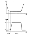
- FIG. 2 is a graph showing the transition of the position and the applied load of the bonding tool 24 in the grounding process and the pressurizing process.
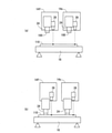
- FIG. 3 is an image diagram showing a state of the bonding process of this example
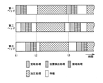
- FIG. 4 is a diagram showing an example of a timing chart of the bonding process of this example.
- FIG. 7 is an image diagram showing a state of the bonding process of the comparative example
- FIG. 8 is a diagram showing an example of the timing chart of the bonding process of the comparative example.
- the comparative example is a process that emphasizes shortening the processing time of the bonding process.
- the controller 18 causes each bonding head 14 to sequentially execute a receiving process, a positioning process, a grounding process, and a pressurizing process.
- the receiving process is a process of receiving a new semiconductor chip 100 from the pickup unit 12.
- the controller 34 positions the bonding tool 24 in the horizontal direction so that the bonding terminal of the semiconductor chip 100 held by the bonding tool 24 is located directly above the corresponding electrode of the substrate 110. Execute the process.
- this positioning process as shown in FIGS. 3A or 7A, the substrate 110 is imaged by the head camera 26, and the bonding head 14 is positioned horizontally with respect to the substrate 110 based on the obtained image. To get.
- the controller 34 lowers the bonding tool 24 and executes a grounding process for grounding the semiconductor chip 100 to the substrate 110, as shown in FIG. 3 (b) or FIG. 7 (b). Then, when the grounding process is completed, the controller 34 executes a pressurizing process of applying a predetermined bonding load Fb to the semiconductor chip 100 with the bonding tool 24. By adding the joining load Fb, the joining terminal of the semiconductor chip 100 is joined to the electrode of the substrate 110. When this load is applied, the substrate 110 and the semiconductor chip 100 may be heated to a temperature lower than the melting temperature of the electrodes and the bonding terminals by the heaters provided on the stage 16 and the bonding tool 24.
- FIG. 2 shows the transition of the Z position of the bonding tool 24 in the grounding treatment and the pressure treatment
- the lower part of FIG. 2 shows the transition of the additional load in the grounding treatment and the pressure treatment.
- the controller 18 drives the elevating mechanism provided on the bonding head 14 to start the pressurizing process of applying the predetermined joining load Fb to the semiconductor chip 100.
- the controller 34 raises the bonding tool 24 and ends the pressurization process.
- the receiving process by the first head 14f and the receiving process by the second head 14s cannot be executed in parallel.
- the second head 14s is other than the receiving process.
- the process (pressurization process in the illustrated example) is executed, and during the execution period t11 to t12 of the receiving process by the second head 14s, the first head 14f performs a process other than the receiving process (positioning process and grounding process in the illustrated example). Just do it.
- the waiting time for the bonding head 14 to stand by without doing anything can be eliminated, and the time required for manufacturing the semiconductor device can be shortened.
- the positioning accuracy of the other bonding head 14 may decrease due to the pressurization process by the one bonding head 14. That is, in the comparative example, as shown in FIG. 8, during the period (t12 to t14) in which the first head 14f is executing the pressurizing process, the second head 14s performs the positioning process (region of the lattice hatching) and Grounding processing (horizontal line hatching area) is being performed. In the pressurizing treatment, as described above, a relatively large joining load Fb is applied to the substrate 110 and thus to the stage 16. As a result, the stage 16 and the substrate 110 may bend around the pressed portion as shown in FIG. 7 (b).
- the horizontal position of the second head 14s with respect to the substrate 110 is displaced as compared with the state where the stage 16 is horizontal. Therefore, when the stage 16 is bent due to the pressurization treatment of the first head 14f and the positioning treatment or the grounding treatment is performed by the second head 14s, the semiconductor chip 100 held by the second head 14s is appropriate. It cannot be grounded at a suitable position, and the position accuracy of the chip joint is reduced.
- the execution period of the pressurization process of the first head 14f and the execution period of the pressurization process of the second head 14s are at least partially overlapped, while the positioning process and the grounding process are performed by either bonding.
- the head 14 is also configured to allow only during the non-pressurization period in which the pressurization process is not executed. That is, as shown in FIG. 4, even if the grounding process is completed at time t3, the first head 14f does not start the pressurizing process until the time t4 when the grounding process of the second head 14s is completed. , Waiting. Then, the pressurizing process of the first head 14f is started after the time t4 when the grounding process of the second head 14s is completed.
- the positioning process and the grounding process of the second head 14s are not executed, and the pressurization of the second head 14s is performed.
- the positioning process and the grounding process of the first head 14f are not executed.
- the time required for the pressurization process is several to ten times longer than the time required from the receiving process to the completion of the grounding process.
- the waiting time of the bonding heads 14 can be shortened, and the increase in the time required for manufacturing the semiconductor device can be suppressed to a small extent.
- the pressurization process of the first head 14f and the pressurization process of the second head 14s are started at the same time.
- the start timing of the pressurizing process of the two bonding heads 14 does not necessarily have to be simultaneous as long as the grounding process of both the first head 14f and the second head 14s is completed.
- the start timing of the pressurization process of the two bonding heads 14 is set. It does not have to match. However, since it is desirable that the load applied to the stage 16 is less biased, it is desirable that the start timings of the pressurizing treatments of the two bonding heads 14 are substantially the same.
- the position accuracy of the semiconductor chip 100 can be further improved.
- the configuration described so far is an example, and the positioning process and the grounding process are independently performed on the plurality of bonding heads 14 during the non-pressurizing period in which none of the bonding heads 14 is subjected to the pressurizing process.
- Other configurations are such that at least two bonding heads 14 that have been executed and have completed the positioning process and the grounding process are subjected to the pressurizing process in parallel so that the execution periods are at least partially overlapped. , May be changed as appropriate.
- the number of bonding heads 14 provided in one manufacturing apparatus 10 is not limited to two, and may be larger.
- FIG. 5 is an example of a timing chart when one manufacturing apparatus 10 has three bonding heads 14. In the example of FIG. 5, the pressure processing of each bonding head 14 is started after the time t2 when the grounding processing of all three bonding heads 14 is completed. Further, as shown in FIG. 5, the start timings of the pressurizing treatments of the plurality of bonding heads 14 do not have to be simultaneous and may be different.
- the bonding head 14 is provided with only one pickup unit 12 for passing a new semiconductor chip 100, but the number of pickup units 12 may be the same as that of the bonding head 14.
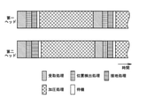
- FIG. 6 is an example of a timing chart when two pickup units 12 and two bonding heads 14 are provided. In this case, the pickup unit 12 supplies a new semiconductor chip 100 to the corresponding bonding head 14, respectively.
- the two bonding heads 14 can execute the receiving process in parallel, and the start timings of the positioning process, the grounding process, and the pressurizing process, which are performed thereafter, can be made substantially the same.
Landscapes
- Engineering & Computer Science (AREA)
- Mechanical Engineering (AREA)
- Manufacturing & Machinery (AREA)
- Microelectronics & Electronic Packaging (AREA)
- Physics & Mathematics (AREA)
- Optics & Photonics (AREA)
- Wire Bonding (AREA)
- Die Bonding (AREA)
Abstract
Description
Claims (5)
- 基板が載置されるステージと、
チップを保持して鉛直方向に移動可能なボンディングツールを有し、互いに独立して水平に移動可能な複数のボンディングヘッドと、
前記複数のボンディングヘッドそれぞれに、水平方向に位置決めする位置決め処理と、前記チップが前記基板または他のチップに接地するまで下降する接地処理と、接地させた前記チップにボンディングのための荷重を付加する加圧処理と、を実行させるコントローラと、
を備え、前記コントローラは、いずれのボンディングヘッドも前記加圧処理を実行していない非加圧期間中に、前記複数のボンディングヘッドに前記位置決め処理および前記接地処理を互いに独立して実行させ、前記位置決め処理および前記接地処理を終えた少なくとも二つのボンディングヘッドに、前記加圧処理を、その実行期間が少なくとも部分的に重複するように、並行して実行させる、
ことを特徴とする半導体装置の製造装置。 - 請求項1に記載の半導体装置の製造装置であって、
前記コントローラは、前記少なくとも二つのボンディングヘッドを、それぞれ、自身の接地処理が完了した後、他のボンディングヘッドによる接地処理が完了するまで、接地状態のまま待機させる、ことを特徴とする半導体装置の製造装置。 - 請求項1または2に記載の半導体装置の製造装置であって、さらに、
前記複数のボンディングヘッドに、新たな前記チップを順番に供給する単一のピックアップユニットを備え、
前記コントローラは、前記複数のボンディングヘッドによる、新たなチップを受け取る受取処理の実行時間が、互いに重複しないように、前記複数のボンディングヘッドの前記受取処理の実行タイミングをずらす、
ことを特徴とする半導体装置の製造装置。 - 請求項1または2に記載の半導体装置の製造装置であって、さらに、
前記複数のボンディングヘッドそれぞれに対応して設けられ、対応するボンディングヘッドに、新たな前記チップを供給する複数のピックアップユニットを備え、
前記コントローラは、前記複数のボンディングヘッドそれぞれに、新たなチップを受け取る受取処理と、前記位置決め処理と、前記接地処理と、前記加圧処理とを、互いに並行して実行させるとともに、前記接地処理と前記加圧処理との間に所定の待機時間を設けている、ことを特徴とする半導体装置の製造装置。 - ステージに載置された基板に、チップをボンディングして半導体装置を製造する半導体装置の製造方法であって、
前記チップを保持して鉛直方向に移動可能なボンディングツールを有し、互いに独立して水平に移動可能な複数のボンディングヘッドそれぞれが、水平方向に位置決めする位置決めステップと、前記チップが前記基板または他のチップに接地するまで下降する接地ステップと、接地させた前記チップにボンディングのための荷重を付加する加圧ステップと、を実行し、
前記複数のボンディングヘッドは、いずれのボンディングヘッドも前記加圧ステップを実行していない非加圧期間中に、前記位置決めステップおよび前記接地ステップを互いに独立して実行し、
前記位置決めステップおよび前記接地ステップを終えた少なくとも二つのボンディングヘッドは、前記加圧ステップを、その実行期間が少なくとも部分的に重複するように、並行して実行する、
ことを特徴とする半導体装置の製造方法。
Priority Applications (6)
| Application Number | Priority Date | Filing Date | Title |
|---|---|---|---|
| PCT/JP2020/033336 WO2022049685A1 (ja) | 2020-09-02 | 2020-09-02 | 半導体装置の製造装置および製造方法 |
| CN202080103194.1A CN115868014B (zh) | 2020-09-02 | 2020-09-02 | 半导体装置的制造装置以及制造方法 |
| JP2022546789A JP7493836B2 (ja) | 2020-09-02 | 2020-09-02 | 半導体装置の製造装置および製造方法 |
| KR1020237006013A KR102719256B1 (ko) | 2020-09-02 | 2020-09-02 | 반도체 장치의 제조 장치 및 제조 방법 |
| US18/024,268 US20230268313A1 (en) | 2020-09-02 | 2020-09-02 | Semiconductor device manufacturing device and manufacturing method |
| TW110132491A TWI827972B (zh) | 2020-09-02 | 2021-09-01 | 半導體裝置的製造裝置以及製造方法 |
Applications Claiming Priority (1)
| Application Number | Priority Date | Filing Date | Title |
|---|---|---|---|
| PCT/JP2020/033336 WO2022049685A1 (ja) | 2020-09-02 | 2020-09-02 | 半導体装置の製造装置および製造方法 |
Publications (1)
| Publication Number | Publication Date |
|---|---|
| WO2022049685A1 true WO2022049685A1 (ja) | 2022-03-10 |
Family
ID=80491874
Family Applications (1)
| Application Number | Title | Priority Date | Filing Date |
|---|---|---|---|
| PCT/JP2020/033336 Ceased WO2022049685A1 (ja) | 2020-09-02 | 2020-09-02 | 半導体装置の製造装置および製造方法 |
Country Status (6)
| Country | Link |
|---|---|
| US (1) | US20230268313A1 (ja) |
| JP (1) | JP7493836B2 (ja) |
| KR (1) | KR102719256B1 (ja) |
| CN (1) | CN115868014B (ja) |
| TW (1) | TWI827972B (ja) |
| WO (1) | WO2022049685A1 (ja) |
Citations (7)
| Publication number | Priority date | Publication date | Assignee | Title |
|---|---|---|---|---|
| JPH06177179A (ja) * | 1992-12-01 | 1994-06-24 | Toshiba Corp | チップ部品マウント装置およびその荷重制御方法 |
| JP2002368021A (ja) * | 2001-06-06 | 2002-12-20 | Mitsubishi Electric Corp | ボンディング装置 |
| JP2004303757A (ja) * | 2003-03-28 | 2004-10-28 | Japan Aviation Electronics Industry Ltd | ボンディング装置 |
| JP2011040489A (ja) * | 2009-08-07 | 2011-02-24 | Shibaura Mechatronics Corp | 電子部品の実装装置及び実装方法 |
| JP2012028587A (ja) * | 2010-07-23 | 2012-02-09 | Yamaha Motor Co Ltd | 実装機 |
| WO2014157134A1 (ja) * | 2013-03-28 | 2014-10-02 | 東レエンジニアリング株式会社 | 実装方法および実装装置 |
| US20200083193A1 (en) * | 2018-09-11 | 2020-03-12 | Pyxis Cf Pte. Ltd. | Apparatus and method for semiconductor device bonding |
Family Cites Families (14)
| Publication number | Priority date | Publication date | Assignee | Title |
|---|---|---|---|---|
| JP2888073B2 (ja) | 1993-01-18 | 1999-05-10 | 松下電器産業株式会社 | タブデバイスの熱圧着装置および熱圧着方法 |
| JPH11251366A (ja) * | 1998-03-02 | 1999-09-17 | Hitachi Ltd | 半導体装置の製造方法および装置 |
| JP2002324821A (ja) | 2001-04-25 | 2002-11-08 | Matsushita Electric Ind Co Ltd | 電子部品の圧着装置及び圧着方法 |
| JP5167779B2 (ja) * | 2007-11-16 | 2013-03-21 | ルネサスエレクトロニクス株式会社 | 半導体装置の製造方法 |
| US20140069989A1 (en) * | 2012-09-13 | 2014-03-13 | Texas Instruments Incorporated | Thin Semiconductor Chip Mounting |
| KR101566714B1 (ko) * | 2013-07-25 | 2015-11-13 | 한미반도체 주식회사 | 플립칩 본딩장치 |
| JP6490522B2 (ja) * | 2015-07-14 | 2019-03-27 | 東レエンジニアリング株式会社 | 半導体実装装置 |
| JP6681241B2 (ja) * | 2016-03-30 | 2020-04-15 | アスリートFa株式会社 | 電子部品実装装置および電子部品製造方法 |
| KR101834644B1 (ko) * | 2016-06-30 | 2018-03-05 | 세메스 주식회사 | 다이 본딩 장치 |
| JP6816992B2 (ja) * | 2016-08-08 | 2021-01-20 | 東レエンジニアリング株式会社 | 実装装置 |
| JP6349538B2 (ja) * | 2016-09-30 | 2018-07-04 | 株式会社新川 | 半導体装置の製造方法および実装装置 |
| JP6789791B2 (ja) * | 2016-12-13 | 2020-11-25 | 東レエンジニアリング株式会社 | 半導体装置の製造装置および製造方法 |
| TWI702695B (zh) * | 2017-12-01 | 2020-08-21 | 日商新川股份有限公司 | 封裝裝置 |
| KR102568388B1 (ko) * | 2018-06-04 | 2023-08-18 | 한화정밀기계 주식회사 | 본딩 장치 |
-
2020
- 2020-09-02 CN CN202080103194.1A patent/CN115868014B/zh active Active
- 2020-09-02 KR KR1020237006013A patent/KR102719256B1/ko active Active
- 2020-09-02 JP JP2022546789A patent/JP7493836B2/ja active Active
- 2020-09-02 WO PCT/JP2020/033336 patent/WO2022049685A1/ja not_active Ceased
- 2020-09-02 US US18/024,268 patent/US20230268313A1/en active Pending
-
2021
- 2021-09-01 TW TW110132491A patent/TWI827972B/zh active
Patent Citations (7)
| Publication number | Priority date | Publication date | Assignee | Title |
|---|---|---|---|---|
| JPH06177179A (ja) * | 1992-12-01 | 1994-06-24 | Toshiba Corp | チップ部品マウント装置およびその荷重制御方法 |
| JP2002368021A (ja) * | 2001-06-06 | 2002-12-20 | Mitsubishi Electric Corp | ボンディング装置 |
| JP2004303757A (ja) * | 2003-03-28 | 2004-10-28 | Japan Aviation Electronics Industry Ltd | ボンディング装置 |
| JP2011040489A (ja) * | 2009-08-07 | 2011-02-24 | Shibaura Mechatronics Corp | 電子部品の実装装置及び実装方法 |
| JP2012028587A (ja) * | 2010-07-23 | 2012-02-09 | Yamaha Motor Co Ltd | 実装機 |
| WO2014157134A1 (ja) * | 2013-03-28 | 2014-10-02 | 東レエンジニアリング株式会社 | 実装方法および実装装置 |
| US20200083193A1 (en) * | 2018-09-11 | 2020-03-12 | Pyxis Cf Pte. Ltd. | Apparatus and method for semiconductor device bonding |
Also Published As
| Publication number | Publication date |
|---|---|
| JP7493836B2 (ja) | 2024-06-03 |
| CN115868014A (zh) | 2023-03-28 |
| KR102719256B1 (ko) | 2024-10-17 |
| TW202222144A (zh) | 2022-06-01 |
| CN115868014B (zh) | 2025-08-01 |
| TWI827972B (zh) | 2024-01-01 |
| KR20230041776A (ko) | 2023-03-24 |
| US20230268313A1 (en) | 2023-08-24 |
| JPWO2022049685A1 (ja) | 2022-03-10 |
Similar Documents
| Publication | Publication Date | Title |
|---|---|---|
| CN1153267C (zh) | 半导体器件的制造方法 | |
| JP6787613B2 (ja) | 実装装置 | |
| WO2014171160A1 (ja) | 半導体装置および半導体装置の製造方法 | |
| JP2015079832A (ja) | 薄基板の矯正方法および矯正装置 | |
| JP7493836B2 (ja) | 半導体装置の製造装置および製造方法 | |
| TWI729246B (zh) | 半導體裝置的製造裝置及製造方法 | |
| JP7122606B2 (ja) | 熱圧着装置及び熱圧着方法 | |
| CN114050136A (zh) | 一种芯片焊盘植球整平及二次焊接的方法 | |
| CN206210755U (zh) | 用于固定衬底的设备和用于减少衬底中的翘曲的设备 | |
| US7284686B2 (en) | Mounting method of bump-equipped electronic component and mounting structure of the same | |
| JPH01244630A (ja) | 半導体ペレットのボンディング方法 | |
| JP7122607B2 (ja) | 熱圧着装置及び熱圧着方法 | |
| JP4601844B2 (ja) | ボンディング装置及びボンディンク方法 | |
| JP2576426B2 (ja) | 半導体装置のボンディング方法及びボンディング装置 | |
| JP6863767B2 (ja) | 実装装置および実装方法 | |
| JP7317354B2 (ja) | 実装装置 | |
| TWI897221B (zh) | 接合半導體晶片的方法及接合裝置 | |
| JP2004228202A (ja) | 半導体装置およびその製造方法 | |
| JP4228839B2 (ja) | ボンディング装置 | |
| JP3253761B2 (ja) | アウタリ−ドボンディング装置および方法 | |
| TWI288977B (en) | Method for adjusting coplanarity calibration of a thermocompression head | |
| JP7023700B2 (ja) | 実装装置及び実装方法 | |
| CN119650460A (zh) | 芯片贴装装置、安装方法以及半导体器件的制造方法 | |
| US9847313B2 (en) | Thermocompression bonders, methods of operating thermocompression bonders, and horizontal scrub motions in thermocompression bonding | |
| JPH0917826A (ja) | 半導体製造装置及び方法 |
Legal Events
| Date | Code | Title | Description |
|---|---|---|---|
| 121 | Ep: the epo has been informed by wipo that ep was designated in this application |
Ref document number: 20952424 Country of ref document: EP Kind code of ref document: A1 |
|
| DPE1 | Request for preliminary examination filed after expiration of 19th month from priority date (pct application filed from 20040101) | ||
| ENP | Entry into the national phase |
Ref document number: 2022546789 Country of ref document: JP Kind code of ref document: A |
|
| ENP | Entry into the national phase |
Ref document number: 20237006013 Country of ref document: KR Kind code of ref document: A |
|
| NENP | Non-entry into the national phase |
Ref country code: DE |
|
| 122 | Ep: pct application non-entry in european phase |
Ref document number: 20952424 Country of ref document: EP Kind code of ref document: A1 |
|
| WWG | Wipo information: grant in national office |
Ref document number: 202080103194.1 Country of ref document: CN |