WO2022004409A1 - アンテナ付き半導体パッケージ及びアンテナ付き半導体パッケージ用樹脂組成物 - Google Patents
アンテナ付き半導体パッケージ及びアンテナ付き半導体パッケージ用樹脂組成物 Download PDFInfo
- Publication number
- WO2022004409A1 WO2022004409A1 PCT/JP2021/023019 JP2021023019W WO2022004409A1 WO 2022004409 A1 WO2022004409 A1 WO 2022004409A1 JP 2021023019 W JP2021023019 W JP 2021023019W WO 2022004409 A1 WO2022004409 A1 WO 2022004409A1
- Authority
- WO
- WIPO (PCT)
- Prior art keywords
- antenna
- semiconductor package
- styrene
- resin composition
- insulating layer
- Prior art date
- Legal status (The legal status is an assumption and is not a legal conclusion. Google has not performed a legal analysis and makes no representation as to the accuracy of the status listed.)
- Ceased
Links
Images


Classifications
-
- H—ELECTRICITY
- H01—ELECTRIC ELEMENTS
- H01Q—ANTENNAS, i.e. RADIO AERIALS
- H01Q1/00—Details of, or arrangements associated with, antennas
- H01Q1/12—Supports; Mounting means
- H01Q1/22—Supports; Mounting means by structural association with other equipment or articles
- H01Q1/2283—Supports; Mounting means by structural association with other equipment or articles mounted in or on the surface of a semiconductor substrate as a chip-type antenna or integrated with other components into an IC package
-
- C—CHEMISTRY; METALLURGY
- C08—ORGANIC MACROMOLECULAR COMPOUNDS; THEIR PREPARATION OR CHEMICAL WORKING-UP; COMPOSITIONS BASED THEREON
- C08L—COMPOSITIONS OF MACROMOLECULAR COMPOUNDS
- C08L27/00—Compositions of homopolymers or copolymers of compounds having one or more unsaturated aliphatic radicals, each having only one carbon-to-carbon double bond, and at least one being terminated by a halogen; Compositions of derivatives of such polymers
- C08L27/02—Compositions of homopolymers or copolymers of compounds having one or more unsaturated aliphatic radicals, each having only one carbon-to-carbon double bond, and at least one being terminated by a halogen; Compositions of derivatives of such polymers not modified by chemical after-treatment
- C08L27/12—Compositions of homopolymers or copolymers of compounds having one or more unsaturated aliphatic radicals, each having only one carbon-to-carbon double bond, and at least one being terminated by a halogen; Compositions of derivatives of such polymers not modified by chemical after-treatment containing fluorine atoms
- C08L27/18—Homopolymers or copolymers or tetrafluoroethene
-
- C—CHEMISTRY; METALLURGY
- C08—ORGANIC MACROMOLECULAR COMPOUNDS; THEIR PREPARATION OR CHEMICAL WORKING-UP; COMPOSITIONS BASED THEREON
- C08L—COMPOSITIONS OF MACROMOLECULAR COMPOUNDS
- C08L53/00—Compositions of block copolymers containing at least one sequence of a polymer obtained by reactions only involving carbon-to-carbon unsaturated bonds; Compositions of derivatives of such polymers
- C08L53/02—Compositions of block copolymers containing at least one sequence of a polymer obtained by reactions only involving carbon-to-carbon unsaturated bonds; Compositions of derivatives of such polymers of vinyl-aromatic monomers and conjugated dienes
-
- C—CHEMISTRY; METALLURGY
- C08—ORGANIC MACROMOLECULAR COMPOUNDS; THEIR PREPARATION OR CHEMICAL WORKING-UP; COMPOSITIONS BASED THEREON
- C08L—COMPOSITIONS OF MACROMOLECULAR COMPOUNDS
- C08L63/00—Compositions of epoxy resins; Compositions of derivatives of epoxy resins
-
- H—ELECTRICITY
- H01—ELECTRIC ELEMENTS
- H01B—CABLES; CONDUCTORS; INSULATORS; SELECTION OF MATERIALS FOR THEIR CONDUCTIVE, INSULATING OR DIELECTRIC PROPERTIES
- H01B3/00—Insulators or insulating bodies characterised by the insulating materials; Selection of materials for their insulating or dielectric properties
- H01B3/18—Insulators or insulating bodies characterised by the insulating materials; Selection of materials for their insulating or dielectric properties mainly consisting of organic substances
- H01B3/30—Insulators or insulating bodies characterised by the insulating materials; Selection of materials for their insulating or dielectric properties mainly consisting of organic substances plastics; resins; waxes
- H01B3/44—Insulators or insulating bodies characterised by the insulating materials; Selection of materials for their insulating or dielectric properties mainly consisting of organic substances plastics; resins; waxes vinyl resins; acrylic resins
- H01B3/442—Insulators or insulating bodies characterised by the insulating materials; Selection of materials for their insulating or dielectric properties mainly consisting of organic substances plastics; resins; waxes vinyl resins; acrylic resins from aromatic vinyl compounds
-
- H—ELECTRICITY
- H01—ELECTRIC ELEMENTS
- H01Q—ANTENNAS, i.e. RADIO AERIALS
- H01Q1/00—Details of, or arrangements associated with, antennas
- H01Q1/36—Structural form of radiating elements, e.g. cone, spiral, umbrella; Particular materials used therewith
- H01Q1/38—Structural form of radiating elements, e.g. cone, spiral, umbrella; Particular materials used therewith formed by a conductive layer on an insulating support
-
- H—ELECTRICITY
- H05—ELECTRIC TECHNIQUES NOT OTHERWISE PROVIDED FOR
- H05K—PRINTED CIRCUITS; CASINGS OR CONSTRUCTIONAL DETAILS OF ELECTRIC APPARATUS; MANUFACTURE OF ASSEMBLAGES OF ELECTRICAL COMPONENTS
- H05K3/00—Apparatus or processes for manufacturing printed circuits
- H05K3/46—Manufacturing multilayer circuits
-
- H—ELECTRICITY
- H10—SEMICONDUCTOR DEVICES; ELECTRIC SOLID-STATE DEVICES NOT OTHERWISE PROVIDED FOR
- H10W—GENERIC PACKAGES, INTERCONNECTIONS, CONNECTORS OR OTHER CONSTRUCTIONAL DETAILS OF DEVICES COVERED BY CLASS H10
- H10W44/00—Electrical arrangements for controlling or matching impedance
- H10W44/20—Electrical arrangements for controlling or matching impedance at high-frequency [HF] or radio frequency [RF]
-
- H—ELECTRICITY
- H10—SEMICONDUCTOR DEVICES; ELECTRIC SOLID-STATE DEVICES NOT OTHERWISE PROVIDED FOR
- H10W—GENERIC PACKAGES, INTERCONNECTIONS, CONNECTORS OR OTHER CONSTRUCTIONAL DETAILS OF DEVICES COVERED BY CLASS H10
- H10W70/00—Package substrates; Interposers; Redistribution layers [RDL]
- H10W70/60—Insulating or insulated package substrates; Interposers; Redistribution layers
- H10W70/67—Insulating or insulated package substrates; Interposers; Redistribution layers characterised by their insulating layers or insulating parts
- H10W70/69—Insulating materials thereof
-
- H—ELECTRICITY
- H10—SEMICONDUCTOR DEVICES; ELECTRIC SOLID-STATE DEVICES NOT OTHERWISE PROVIDED FOR
- H10W—GENERIC PACKAGES, INTERCONNECTIONS, CONNECTORS OR OTHER CONSTRUCTIONAL DETAILS OF DEVICES COVERED BY CLASS H10
- H10W74/00—Encapsulations, e.g. protective coatings
- H10W74/10—Encapsulations, e.g. protective coatings characterised by their shape or disposition
- H10W74/111—Encapsulations, e.g. protective coatings characterised by their shape or disposition the semiconductor body being completely enclosed
- H10W74/114—Encapsulations, e.g. protective coatings characterised by their shape or disposition the semiconductor body being completely enclosed by a substrate and the encapsulations
- H10W74/117—Encapsulations, e.g. protective coatings characterised by their shape or disposition the semiconductor body being completely enclosed by a substrate and the encapsulations the substrate having spherical bumps for external connection
-
- H—ELECTRICITY
- H10—SEMICONDUCTOR DEVICES; ELECTRIC SOLID-STATE DEVICES NOT OTHERWISE PROVIDED FOR
- H10W—GENERIC PACKAGES, INTERCONNECTIONS, CONNECTORS OR OTHER CONSTRUCTIONAL DETAILS OF DEVICES COVERED BY CLASS H10
- H10W44/00—Electrical arrangements for controlling or matching impedance
- H10W44/20—Electrical arrangements for controlling or matching impedance at high-frequency [HF] or radio frequency [RF]
- H10W44/241—Electrical arrangements for controlling or matching impedance at high-frequency [HF] or radio frequency [RF] for passive devices or passive elements
- H10W44/248—Electrical arrangements for controlling or matching impedance at high-frequency [HF] or radio frequency [RF] for passive devices or passive elements for antennas
Definitions
- the present invention relates to a semiconductor package with an antenna and a resin composition for a semiconductor package with an antenna. More specifically, the present invention relates to a semiconductor package with an antenna having excellent solder heat resistance and low transmission loss, and a resin composition for a semiconductor package with an antenna.
- the 5G millimeter wave antenna requires a structure that shortens the wiring distance between the antenna and the IC to reduce the conductor loss (in other words, the transmission loss is small) in terms of packaging technology. For this reason, in recent years, semiconductor packages with antennas (for example, antenna-in-package (AiP) and antenna-on-package (AoP)) in which the antenna portion is integrally formed with the semiconductor device portion have been developed (for example, for example). See Non-Patent Documents 1 and 2).
- Manufacturing of a semiconductor package with an antenna includes a solder reflow process for soldering inside the semiconductor device unit. Therefore, the semiconductor package with an antenna is required to have solder heat resistance.
- the insulating layer for connecting the semiconductor device portion and the antenna portion and the insulating layer inside the antenna portion are also required to have solder heat resistance.
- the above-mentioned insulating layer is also required to have high frequency characteristics.
- the present invention has been made in view of the problems of the prior art.
- the present invention provides a semiconductor package with an antenna having excellent solder heat resistance and low transmission loss, and a resin composition for a semiconductor package with an antenna used for such a semiconductor package with an antenna.
- the following semiconductor package with an antenna and the resin composition for a semiconductor package with an antenna are provided.
- the insulating layer for connecting the semiconductor device portion and the antenna portion, or the insulating layer inside the antenna portion is A semiconductor package with an antenna, which is a cured product of a resin composition containing (A) a styrene-based elastomer having a double bond and (B) a compound that generates radicals.
- the total mass of the epoxy resin and the curing agent in the cured product is 5 with respect to the total mass of 100 parts by mass of the styrene-based elastoma having the (A) double bond and the compound generating the (B) radical.
- a resin composition for a semiconductor package with an antenna which comprises (A) a styrene-based elastomer having a double bond and (B) a compound that generates radicals.
- the total mass of the epoxy resin and the curing agent in the resin composition is 5 with respect to the total of 100 parts by mass of the styrene-based elastomer having the (A) double bond and the compound that generates the (B) radical.
- the semiconductor package with an antenna of the present invention has the effects of excellent solder heat resistance and low transmission loss. Further, the resin composition for a semiconductor package with an antenna of the present invention has an effect that a semiconductor package with an antenna having excellent solder heat resistance and low transmission loss can be realized.
- FIG. 1 is a schematic partial cross-sectional view showing a semiconductor package with an antenna according to an embodiment of the present invention.
- the antenna unit 5 is integrally formed with the semiconductor device unit 10, and in particular, 5G millimeter wave transmission / reception communication is performed. It is a semiconductor package 100 with an antenna as a high frequency substrate on which an RF (radio frequency) chip 8 is mounted.
- the antenna unit 5 is connected to the RF chip 8 that performs millimeter-wave communication in the semiconductor device unit 10 by a wiring layer 4 having various wiring patterns.
- the semiconductor device unit 10 in the semiconductor package 100 with an antenna shown in FIG. 1 includes a core substrate 2, an antenna unit 5 arranged on one surface side of the semiconductor device unit 10, and a semiconductor device unit 10 and an antenna unit 5.
- An insulating layer 1 (first insulating layer 1A) for connection, a wiring layer 4 having a multi-layer structure arranged in a core substrate 2, and an insulating layer 1 configured to cover wiring vias in the wiring layer 4.
- second, third insulating layer 1C, fourth insulating layer 1D, fifth insulating layer 1E are included.
- the first insulating layer 1A is provided not only to be interposed between the semiconductor device unit 10 and the antenna unit 5, but also to extend to the inside of the antenna unit 5. You may.
- one part of the wiring layer 4 is connected to the RF chip 8 that performs millimeter wave transmission / reception communication on the other surface side of the semiconductor device unit 10, and the other of the wiring layer 4 is connected to the RF chip 8.
- the portion of is connected to the electrically connected metal 7.
- the wiring layer 4 and the RF chip 8 are electrically connected via a hemispherical connection pad 9.
- the electrically connecting metal 7 is a terminal portion for physically and / or electrically connecting the semiconductor package 100 with an antenna and the outside through the electrically connecting metal 7 according to its function.
- the insulating layer 1 transmits the current and millimeter wave signals output from the RF chip 8 at the time of transmission to the antenna unit 5 and efficiently radiates them into the space, so that the antenna unit 5 and the RF chip 8 can be efficiently radiated. It is required to reduce the loss (transmission loss) of the connection part connecting the two. The same applies to reception, and in order to transmit to the RF chip 8 as a receiving unit while suppressing the attenuation of the reflected wave of the millimeter wave signal received by the antenna unit 5, the antenna unit 5 and the RF chip 8 are connected to each other. It is required to reduce the loss (transmission loss) of the unit.
- the antenna portion 5 is arranged on one surface side of the semiconductor device portion 10 as a patch antenna as a planar antenna.
- the semiconductor package 100 with an antenna of the present embodiment includes an insulating layer 1 (for example, the first insulating layer 1A) for connecting the semiconductor device unit 10 and the antenna unit 5, or an insulating layer 1 inside the antenna unit 5.
- an insulating layer 1 for example, the first insulating layer 1A
- the configuration of the insulating layer 1 in the antenna-equipped semiconductor package 100 of the present embodiment will be described in more detail.
- the insulating layer 1 for connecting the semiconductor device unit 10 and the antenna unit 5 and the insulating layer 1 inside the antenna unit 5 may be collectively referred to as “insulating layer 1”.
- the insulating layer 1 is a cured product of a resin composition containing (A) a styrene-based elastomer having a double bond and (B) a compound that generates radicals.
- the semiconductor package 100 with an antenna provided with the insulating layer 1 configured in this way has excellent solder heat resistance and can reduce transmission loss.
- a solder test at 288 ° C. may be performed on an insulating layer 1 for connecting the antenna portion 5, which was not necessary in the past. Solder resistance at heat resistant temperature is required.
- the cured product constituting the insulating layer 1 has a dielectric loss tangent (tan ⁇ ) of 0.0020 or less measured at a frequency of 10 GHz by the SPDR (split post dielectric resonator) method. It is preferable that the solder heat resistance is 290 ° C. for 2 minutes or more.
- the insulating layer 1 can be obtained by heat-curing a resin composition containing (A) a styrene-based elastomer having a double bond and (B) a compound that generates radicals.
- styrene-based elastoma having a double bond for example, a block copolymer containing a block of styrene or an analog thereof as at least one terminal block and an elastomer block of a conjugated diene as at least one intermediate block.
- SBS styrene / butadiene / styrene elastomer
- SBBS styrene / butadiene / butylene / styrene elastomer
- the cured product of the resin composition containing a styrene-based elastomer having a double bond has excellent solder heat resistance.
- a styrene-based elastomer having a double bond a styrene-based elastomer containing a styrene / butadiene / butylene / styrene block copolymer can be mentioned as a suitable example.
- the component (A) may be a reactive elastomer imparted with a functional group such as an amine.
- the weight average molecular weight of the component (A) is preferably 20,000 to 200,000, more preferably 30,000 to 150,000.
- the weight average molecular weight is a value using a calibration curve made of standard polystyrene by gel permeation chromatography (GPC).
- Examples of the compound that generates a radical include a decomposable compound and a non-degradable compound.
- the degradable compound include radical generators such as organic peroxides and azo compounds.
- examples of the organic peroxide include benzoyl peroxide, isobutylyl peroxide, isononanoyl peroxide, decanoyyl peroxide, lauroyl peroxide, parachlorobenzoyl peroxide, and di (3,5,5-trimethylhexanoyl) peroxide.
- Diacyl peroxides such as; 2,2-di (4,4-di- (di-tert-butylperoxy) cyclohexyl) peroxyketals such as propane; isopropyl purge carbonate, di-sec-butyl purge carbonate, etc.
- Peroxydicarbonates such as di-2-ethylhexyl purge carbonate, di-1-methylheptyl purge carbonate, di-3-methoxybutyl purge carbonate, dicyclohexyl purge carbonate; tert-butyl perbenzoate, tert-butyl peracetate, tert -Butyl per-2-ethyl hexanoate, tert-butyl perisobutyrate, tert-butyl perpivalate, tert-butyl diper adipate, cumil per neodecanoate, tert-butyl peroxybenzoate, 2,5-dimethyl -Peroxyesters such as 2,5 di (benzoylperoxy) hexane; Ketone peroxides such as methylethylketone peroxide and cyclohexanone peroxide; Di-tert-butyl peroxide, dicumyl peroxide
- the organic peroxide used is not particularly limited, but when the insulating layer 1 is formed from a resin composition or a film containing a solvent, a drying step of about 60 to 80 ° C. is often required. It is preferable to use a film having a 10-hour half-life temperature of 100 ° C to 140 ° C. Further, the 10-hour half-life temperature is more preferably 110 to 130 ° C. Specific examples thereof include dicumyl peroxide. Examples of the azo compound include azo esters. Moreover, as a non-degradable compound, for example, a compound having an ethylenic double bond can be mentioned.
- Examples of the compound having an ethylenically double bond include a modified polyphenylene ether (PPE) having a vinyl group or a styrene group at the terminal, a maleimide compound and the like.
- the number average molecular weight (Mn) of the modified polyphenylene ether (PPE) having a vinyl group or a styrene group at the terminal is preferably in the range of 1000 to 5000, preferably in the range of 1000 to 3000 in terms of polystyrene by the GPC method. More preferably, it is in the range of 1000 to 2500.
- the maleimide compound is preferably a dimer acid-modified bismaleimide having a number average molecular weight of 1000 to 8000.
- the styrene-based elastoma having a double bond is preferably contained in, for example, 25.0 to 99.8% by mass in terms of solid content in the resin composition, and is preferably 30.0 to 85.0% by mass. It is more preferably contained, and further preferably 35.0 to 85.0% by mass.
- the compound (B) that generates radicals is preferably contained in the resin composition in an amount of 0.1 to 70.0% by mass in terms of solid content.
- (B) is preferably contained in the resin composition in an amount of 0.10 to 5% by mass, preferably 0.10 to 2% by mass. It is more preferable, and it is particularly preferable that the content is 0.10 to 1% by mass.
- (B) is preferably contained in the resin composition in an amount of 4 to 70% by mass, more preferably 5 to 30% by mass. It is preferably contained in an amount of 6 to 15% by mass, particularly preferably. With such a configuration, it is possible to further improve the solder heat resistance of the semiconductor package 100 with an antenna and effectively reduce the transmission loss while maintaining the adhesive strength (peel strength).
- the cured product constituting the insulating layer 1 may further contain other components.
- Other components include, for example, cured products of thermosetting resins such as epoxy resins and various curing agents, inorganic fillers such as silica fillers, organic fillers such as PTFE fillers, and various additives such as colorants and dispersants. Can be mentioned.
- the cured product constituting the insulating layer 1 preferably further contains a PTFE filler. By including the PTFE filler, the high frequency characteristics of the semiconductor package 100 with an antenna can be further improved. From the viewpoint of maintaining the adhesive strength (peeling strength), the amount of the inorganic filler or the organic filler is preferably 50% by mass or less in the cured product constituting the insulating layer 1.
- the cured product constituting the insulating layer 1 may contain a cured product of a thermosetting resin such as an epoxy resin, in addition to (A) a styrene-based elastomer having a double bond.
- a thermosetting resin such as an epoxy resin
- the total mass of the epoxy resin component and the curing agent component in the cured product is 10 parts by mass with respect to the total of 100 parts by mass of (A) a styrene-based elastoma having a double bond and (B) a compound that generates a radical. It is preferably less than, and more preferably 5 parts by mass or less.
- the cured product constituting the insulating layer 1 does not include a cured product of the epoxy resin.
- the semiconductor package 100 with an antenna provided with the insulating layer 1 made of a cured product as described above has excellent solder heat resistance and low transmission loss, so that RF for transmitting and receiving 5 G millimeter waves is performed. It is suitably used as a semiconductor package on which a (radio frequency) chip 8 is mounted.
- the first insulating layer 1A for connecting the semiconductor device unit 10 and the antenna unit 5 and the second insulating layer configured to cover the wiring via in the wiring layer 4 are covered. It is preferable that each of the layer 1B, the third insulating layer 1C, the fourth insulating layer 1D, and the fifth insulating layer 1E is configured in the same manner as the insulating layer 1 made of the cured product described above.
- the method for manufacturing the insulating layer 1 in the antenna-equipped semiconductor package 100 of the present embodiment is not particularly limited, and examples thereof include the following methods.
- a resin composition for a semiconductor package with an antenna containing (A) a styrene-based elastomer having a double bond and (B) a compound that generates radicals is prepared.
- the "resin composition for a semiconductor package with an antenna” may be simply referred to as a "resin composition”.
- the resin composition is preferably in the form of a film.
- a solution obtained by adding an organic solvent to a resin composition containing (A) and (B) is applied to a PET film which has been subjected to a mold release treatment as a support. It can be obtained by drying at 80 to 130 ° C.
- a semiconductor package with an antenna can be produced by peeling the obtained film for a semiconductor package with an antenna from a support, attaching the film to the semiconductor device unit 10, and performing heat treatment at 200 ° C. for 30 to 60 minutes, for example. can.
- FIG. 2 is a schematic partial cross-sectional view showing a semiconductor package with an antenna according to another embodiment of the present invention.
- the antenna portions 25 and 26 are integrally formed with the semiconductor device portion 30.
- the antenna units 25 and 26 are connected to the RF chip 28 that performs millimeter wave communication in the semiconductor device unit 10 by a wiring layer 24 having various wiring patterns.
- the semiconductor device unit 30 includes a core substrate 22, an antenna unit 25 arranged on one surface side of the semiconductor device unit 30, and an insulating layer 21 for connecting the semiconductor device unit 30 and the antenna unit 25.
- An RF chip 28 that performs transmission / reception communication of 5 G millimeter waves is housed in the core board 22, and is wired by a wiring layer 24 arranged in the core board 22.
- an antenna unit 26 as a dipole antenna in which linear conductors (elements) are symmetrically arranged is profitable.
- the other surface side of the semiconductor device unit 30 is connected to an electrically connecting metal 27 for physically and / or electrically connecting the semiconductor package 200 with an antenna and the outside.
- the insulating layer 21 is a cured product of a resin composition containing (A) a styrene-based elastomer having a double bond and (B) a compound that generates a radical.
- a cured product used as the insulating layer 21, which has the same structure as the cured product used as the insulating layer 1 of the antenna-equipped semiconductor package 100 shown in FIG. 1, can be adopted.
- the resin composition for an antenna-equipped semiconductor package of the present embodiment is a resin composition for forming the insulating layer 1 of the antenna-equipped semiconductor package 100 as shown in FIG.
- the resin composition for a semiconductor package with an antenna of the present embodiment contains (A) a styrene-based elastomer having a double bond and (B) a compound that generates radicals.
- A a styrene-based elastomer having a double bond
- B a compound that generates radicals.
- Examples of the styrene-based elastomer having a double bond include styrene / butadiene / styrene-based elastomer (SBS), styrene / butadiene / butylene / styrene-based elastomer (SBBS), and the like, as described above. From the viewpoint of high frequency characteristics, a styrene-based elastomer containing a styrene / butadiene / butylene / styrene block copolymer can be mentioned as a suitable example.
- the content of the styrene-based elastomer having a double bond is not particularly limited, and the preferable amount is as described above.
- Examples of the compound that generates a radical include a decomposable compound and a non-degradable compound, as described above.
- Examples of the degradable compound include radical generators such as organic peroxides and azo compounds, and examples of the non-degradable compound include compounds having an ethylenic double bond.
- the content of the compound that generates radicals is not particularly limited, and the preferred amount is as described above.
- the resin composition for a semiconductor package with an antenna of the present embodiment may further contain other components.
- other components include thermosetting resins such as epoxy resins and various curing agents, inorganic fillers such as silica fillers, organic fillers such as PTFE fillers, and various additives such as colorants and dispersants.
- the resin composition for a semiconductor package with an antenna of the present embodiment further contains a PTFE filler.
- the PTFE filler By including the PTFE filler, the high frequency characteristics of the semiconductor package 100 with an antenna can be further improved.
- the amount of the inorganic filler or the organic filler is preferably 50% by mass or less of the resin composition for a semiconductor package with an antenna.
- the total mass of the epoxy resin and the curing agent in the resin composition for the semiconductor package with an antenna is 10 parts by mass with respect to (A) a styrene-based elastoma having a double bond and (B) a compound that generates a radical. It is preferably less than parts by mass, and more preferably 5 parts by mass or less.
- the resin composition for a semiconductor package with an antenna does not contain an epoxy resin.
- Example 1 a resin composition for a semiconductor package with an antenna was prepared as follows. First, as the (A3) styrene-based elastomer of the component (A), 99.75 parts of the styrene-based elastomer (partially hydrogenated) having a double bond was used as a compound that generates the (B1) radical of the component (B). 0.25 parts of a compound that generates a degradable radical was prepared. (A3) As the styrene-based elastomer, the trade name "P1500” manufactured by Asahi Kasei Chemicals Co., Ltd. was used. (B1) As the compound that generates radicals, an organic peroxide trade name “Park Mill D” manufactured by NOF CORPORATION was used.
- this coating liquid was applied to one side of the support and dried at 120 ° C. to obtain an adhesive film with the support.
- a PET film that had undergone a mold release treatment was used as the support.
- a PET film that had undergone a mold release treatment was placed on the obtained adhesive film with a support to obtain a PET film / adhesive film / PET film laminate.
- This film laminate was hot-pressed under heat and pressure conditions of a press temperature of 200 ° C., a temperature holding time of 60 minutes, and a press pressure of 0.98 MPa to heat-cure the adhesive film.
- solder heat resistance test A copper foil with a roughened one side was prepared. A copper foil was laminated with the roughened surface inside to obtain a laminate of copper foil / adhesive film / copper foil. This laminate was thermocompression-bonded at 200 ° C. for 60 minutes at 0.98 MPa using a vacuum press and cured. This test piece was cut into squares so that each side was 30 mm, and a solder heat resistance test sample (test body C) was prepared. Then, the test piece C was floated in a solder bath at 290 ° C., and the presence or absence of swelling was confirmed. The solder heat resistance test was performed in accordance with JIS C 5012 1993. The solder heat resistance test was evaluated according to the following evaluation criteria.
- Examples 2 to 22, Comparative Examples 1 to 3 A resin composition for a semiconductor package with an antenna was prepared in the same manner as in Example 1 except that the formulation of the resin composition for a semiconductor package with an antenna was changed to Tables 1 to 3.
- Example 1 a coating liquid containing the resin compositions for semiconductor packages with antennas of Examples 2 to 22 and Comparative Examples 1 to 3 was applied to one side of the support and dried at 120 ° C. to attach the support.
- Each of the adhesive films was obtained, and a test piece (cured adhesive film) was prepared in the same manner as in Example 1.
- the prepared test pieces were evaluated for dielectric constant ( ⁇ ), dielectric loss tangent (tan ⁇ ), peel strength, and solder heat resistance test by the same method as in Example 1. The results are shown in Tables 1 to 3.
- the raw materials used for preparing the resin composition for a semiconductor package with an antenna in Examples 2 to 22 and Comparative Examples 1 to 3 are as follows.
- (A4) Styrene-based elastomer having a double bond (partially hydrogenated, SBBS), manufactured by Asahi Kasei Chemicals, Inc., trade name "P5051”.
- (A5) Styrene-based elastomer having a double bond (partially hydrogenated, amine-modified SBBS), manufactured by Asahi Kasei Chemicals, trade name "MP10".
- (A6) Styrene-based elastomer (hydrogenated) having no double bond, manufactured by Asahi Kasei Chemicals, Inc., trade name "H1052”.
- (B1) A compound that generates radicals (degradable), manufactured by NOF CORPORATION, trade name "Park Mill D".
- C2) Organic filler, PTFE manufactured by Daikin Industries, Ltd., “Lubron L-5F”.
- the resin composition of Comparative Example 1 did not contain a compound that generates radicals as the component (B), the evaluation results of the peel strength and the solder heat resistance test were very inferior.
- the resin composition of Comparative Example 2 contains a certain amount of organic filler ((C2) PTFE), it does not contain a compound that generates radicals as a component (B), so that the evaluation result of the solder heat resistance test is very high. It was inferior to.
- the resin composition of Comparative Example 3 is a resin composition using a styrene-based elastomer having no double bond as the component (A), and although it has excellent peel strength, the evaluation result of the solder heat resistance test is very inferior. It was a thing.
- the semiconductor package with an antenna of the present invention can be used as a high-frequency substrate on which an RF chip for transmitting / receiving 5 G millimeter waves is mounted.
- the resin composition for an antenna-equipped semiconductor package of the present invention can be used for the insulating layer of the antenna-equipped semiconductor package of the present invention.
Landscapes
- Chemical & Material Sciences (AREA)
- Medicinal Chemistry (AREA)
- Organic Chemistry (AREA)
- Health & Medical Sciences (AREA)
- Polymers & Plastics (AREA)
- Chemical Kinetics & Catalysis (AREA)
- Engineering & Computer Science (AREA)
- Microelectronics & Electronic Packaging (AREA)
- Manufacturing & Machinery (AREA)
- Physics & Mathematics (AREA)
- Spectroscopy & Molecular Physics (AREA)
- Compositions Of Macromolecular Compounds (AREA)
- Macromonomer-Based Addition Polymer (AREA)
- Organic Insulating Materials (AREA)
- Laminated Bodies (AREA)
Abstract
はんだ耐熱性に優れ、且つ、伝送ロスの少ないアンテナ付き半導体パッケージを提供する。半導体装置部10にアンテナ部5が一体的に形成されたアンテナ付き半導体パッケージ100であって、半導体装置部10とアンテナ部5とを接続するための絶縁層1、及びアンテナ部内部の絶縁層1のうちの少なくとも一方が、(A)二重結合を有するスチレン系エラストマと、(B)ラジカルを発生させる化合物とを含む樹脂組成物の硬化物である。
Description
本発明は、アンテナ付き半導体パッケージ及びアンテナ付き半導体パッケージ用樹脂組成物に関する。更に詳しくは、はんだ耐熱性に優れ、且つ、伝送ロスの少ないアンテナ付き半導体パッケージ及びアンテナ付き半導体パッケージ用樹脂組成物に関する。
次世代の通信技術として5Gの標準化が進み、高周波対応の製品を実現する市場要求は高まりつつある。多素子アンテナ技術、高速伝送等の技術開発が加速し、また、高周波帯の利用により通信容量も増え、情報処理能力の向上と同時に高周波ノイズや熱の発生量も増加し、その対策が大きな課題となっている。
5Gミリ波用アンテナでは、パッケージ技術に関してアンテナとICの配線距離を短くして導体損失を低くする(別言すれば、伝送ロスの少ない)構造が必要とされている。このため、近年、アンテナ部が半導体装置部に一体に形成されたアンテナ付き半導体パッケージ(例えば、アンテナ・イン・パッケージ(AiP)やアンテナ・オン・パッケージ(AoP))が開発されている(例えば、非特許文献1及び2参照)。
須藤 薫,他2名,"5Gを実現するミリ波用アンテナ付パッケージング技術",[online],株式会社 村田製作所,[令和2年4月2日検索],インターネット<URL:https://apmc-mwe.org/mwe2019/pdf/WS_01/TH5B-2_1.pdf>
村尾 麻悠子,"フジクラが28GHz帯RF IC開発へ、アンテナと一体型",[online],EE Times Japan,[令和2年4月2日検索],インターネット<URL:https://eetimes.jp/ee/articles/1908/09/news033.html>
アンテナ付き半導体パッケージの製造には、半導体装置部内のはんだ付けを行うための、はんだリフロー工程が含まれる。このため、アンテナ付き半導体パッケージには、はんだ耐熱性が求められる。もちろん、半導体装置部とアンテナ部とを接続するための絶縁層や、アンテナ部内部の絶縁層にもはんだ耐熱性が求められる。上述した絶縁層には、さらに高周波特性も求められる。
本発明は、このような従来技術の有する問題点に鑑みてなされたものである。本発明は、はんだ耐熱性に優れ、且つ、伝送ロスの少ないアンテナ付き半導体パッケージ、及びこのようなアンテナ付き半導体パッケージに用いられるアンテナ付き半導体パッケージ用樹脂組成物を提供する。
本発明によれば、以下に示すアンテナ付き半導体パッケージ及びアンテナ付き半導体パッケージ用樹脂組成物が提供される。
[1] 半導体装置部にアンテナ部が一体的に形成されたアンテナ付き半導体パッケージであって、
前記半導体装置部と前記アンテナ部とを接続するための絶縁層、又は、前記アンテナ部内部の絶縁層が、
(A)二重結合を有するスチレン系エラストマと、(B)ラジカルを発生させる化合物とを含む樹脂組成物の硬化物である、アンテナ付き半導体パッケージ。
前記半導体装置部と前記アンテナ部とを接続するための絶縁層、又は、前記アンテナ部内部の絶縁層が、
(A)二重結合を有するスチレン系エラストマと、(B)ラジカルを発生させる化合物とを含む樹脂組成物の硬化物である、アンテナ付き半導体パッケージ。
[2] 前記硬化物中のエポキシ樹脂及び硬化剤の合計質量が、前記(A)二重結合を有するスチレン系エラストマ及び前記(B)ラジカルを発生させる化合物の合計100質量部に対して、5質量部以下である、前記[1]に記載のアンテナ付き半導体パッケージ。
[3] 前記(A)二重結合を有するスチレン系エラストマが、スチレン/ブタジエン/ブチレン/スチレンブロックコポリマーを含む、前記[1]又は[2]記載のアンテナ付き半導体パッケージ。
[4] 前記硬化物がPTFEフィラーを含む、前記[1]~[3]のいずれかに記載のアンテナ付き半導体パッケージ。
[5] (A)二重結合を有するスチレン系エラストマと、(B)ラジカルを発生させる化合物とを含む、アンテナ付き半導体パッケージ用樹脂組成物。
[6] 樹脂組成物中のエポキシ樹脂及び硬化剤の合計質量が、前記(A)二重結合を有するスチレン系エラストマ及び前記(B)ラジカルを発生させる化合物の合計100質量部に対して、5質量部以下である、前記[5]に記載のアンテナ付き半導体パッケージ用樹脂組成物。
[7] 前記(A)二重結合を有するスチレン系エラストマが、スチレン/ブタジエン/ブチレン/スチレンブロックコポリマーを含む、前記[5]又は[6]記載のアンテナ付き半導体パッケージ用樹脂組成物。
[8] PTFEフィラーを含む、前記[5]~[7]のいずれかに記載のアンテナ付き半導体パッケージ用樹脂組成物。
[9] 前記[5]~[8]のいずれかに記載の樹脂組成物を含むアンテナ付き半導体パッケージ用フィルム。
本発明のアンテナ付き半導体パッケージは、はんだ耐熱性に優れ、且つ、伝送ロスが少ないという効果を奏するものである。また、本発明のアンテナ付き半導体パッケージ用樹脂組成物は、はんだ耐熱性に優れ、且つ、伝送ロスの少ないアンテナ付き半導体パッケージを実現することができるという効果を奏するものである。
以下、本発明の実施の形態について説明するが、本発明は以下の実施の形態に限定されるものではない。したがって、本発明の趣旨を逸脱しない範囲で、当業者の通常の知識に基づいて、以下の実施の形態に対し適宜変更、改良等が加えられたものも本発明の範囲に入ることが理解されるべきである。
(1)アンテナ付き半導体パッケージ:
本発明のアンテナ付き半導体パッケージの一の実施形態は、図1に示すようなアンテナ付き半導体パッケージ100である。図1は、本発明の一の実施形態のアンテナ付き半導体パッケージを示す模式的部分断面図である。
本発明のアンテナ付き半導体パッケージの一の実施形態は、図1に示すようなアンテナ付き半導体パッケージ100である。図1は、本発明の一の実施形態のアンテナ付き半導体パッケージを示す模式的部分断面図である。
図1に示すように、本実施形態のアンテナ付き半導体パッケージ100は、半導体装置部10にアンテナ部5が一体的に形成されたものであり、特に、5Gミリ波の送信・受信の通信を行うRF(無線周波)チップ8が実装される高周波基板としてのアンテナ付き半導体パッケージ100である。アンテナ部5は、半導体装置部10において、ミリ波の通信を行うRFチップ8と各種配線パターンを有する配線層4により接続されている。
図1に示すアンテナ付き半導体パッケージ100における半導体装置部10は、コア基板2と、半導体装置部10の一方の表面側に配設されたアンテナ部5と、半導体装置部10とアンテナ部5とを接続するための絶縁層1(第一絶縁層1A)と、コア基板2内に配置された複層構造の配線層4と、配線層4における配線ビアを被覆するように構成された絶縁層1(第二絶縁層1B、第三絶縁層1C、第四絶縁層1D、第五絶縁層1E)とを含む。なお、第一絶縁層1Aは、半導体装置部10とアンテナ部5との間を介在するように設けられているだけでなく、アンテナ部5の内部にまで延設されるようにして設けられていてもよい。
アンテナ付き半導体パッケージ100は、半導体装置部10の他方の表面側において、配線層4の一部位が、ミリ波の送信・受信の通信を行うRFチップ8と連結されるとともに、配線層4の他の部位が、電気連結金属7と連結されている。図1に示す例では、配線層4とRFチップ8は、半球状の接続パッド9を介して電気的に接続されている。電気連結金属7は、当該電気連結金属7を介して、その機能に合わせて、アンテナ付き半導体パッケージ100と外部とを物理的及び/又は電気的に連結させるための端子部である。
絶縁層1は、送信時においてRFチップ8から出力された電流やミリ波信号が減衰することを抑制しつつ、アンテナ部5に伝えて空間に効率よく放射するため、アンテナ部5とRFチップ8をつなぐ接続部の損失(伝送ロス)を小さくすることが求められる。受信時も同様で、アンテナ部5で受信されたミリ波信号の反射波が減衰することを抑制しつつ、受信部としてのRFチップ8に伝えるには、アンテナ部5とRFチップ8をつなぐ接続部の損失(伝送ロス)を小さくすることが求められる。
アンテナ部5は、平面アンテナとしてのパッチアンテナとして半導体装置部10の一方の表面側に配設されている。
本実施形態のアンテナ付き半導体パッケージ100は、半導体装置部10とアンテナ部5とを接続するための絶縁層1(例えば、第一絶縁層1A)、又は、アンテナ部5内部の絶縁層1の構成に関して特に主要な特徴を有している。以下、本実施形態のアンテナ付き半導体パッケージ100における絶縁層1の構成について更に詳細に説明する。なお、以下、半導体装置部10とアンテナ部5とを接続するための絶縁層1、及びアンテナ部5内部の絶縁層1を総称して、単に「絶縁層1」ということがある。
本実施形態のアンテナ付き半導体パッケージ100において、絶縁層1は、(A)二重結合を有するスチレン系エラストマと、(B)ラジカルを発生させる化合物とを含む樹脂組成物の硬化物である。このように構成された絶縁層1を備えたアンテナ付き半導体パッケージ100は、はんだ耐熱性に優れ、且つ、伝送ロスを少なくすることができる。5Gミリ波用のアンテナ部5を備えたアンテナ付き半導体パッケージ100では、例えば、アンテナ部5を接続するための絶縁層1について、288℃のはんだ試験が行われることがあり、従来では必要なかった耐熱温度での耐はんだ耐熱性が求められる。従来の半導体パッケージにおける絶縁層は、公知の高周波フィルムが使用されているが、このような高周波フィルムは、上述した耐はんだ耐熱性を満たしていないものがあり、5Gミリ波用のアンテナ部5を備えたアンテナ付き半導体パッケージ100に対しての使用できないものが多く含まれている。本実施形態のアンテナ付き半導体パッケージ100において、絶縁層1を構成する硬化物は、SPDR(スプリットポスト誘電体共振器)法にて周波数10GHzで測定した誘電正接(tanδ)が0.0020以下であり、はんだ耐熱が290℃2分以上であることが好ましい。
絶縁層1は、上述した(A)二重結合を有するスチレン系エラストマと、(B)ラジカルを発生させる化合物とを含む樹脂組成物を、加熱硬化することによって得ることができる。
(A)二重結合を有するスチレン系エラストマとしては、例えば、スチレン若しくはその類似体のブロックを少なくとも一つの末端ブロックとして含み、共役ジエンのエラストマーブロックを少なくとも一つの中間ブロックとして含むブロック共重合体を挙げることができる。例えば、スチレン/ブタジエン/スチレン系エラストマ(SBS)、スチレン/ブタジエン/ブチレン/スチレン系エラストマ(SBBS)等を挙げることができる。(A)二重結合を有するスチレン系エラストマを含む樹脂組成物の硬化物は、はんだ耐熱性に優れたものとなる。特に、高周波特性の観点から、(A)二重結合を有するスチレン系エラストマとして、スチレン/ブタジエン/ブチレン/スチレンブロックコポリマーを含むスチレン系エラストマを好適例として挙げることができる。(A)成分は、アミンなどの官能基が付与された反応性のエラストマであってもよい。官能基が付与された反応性のエラストマを使用することで、接着強度(ピール強度)をより向上させることができる。(A)成分の重量平均分子量は、20,000~200,000であるものが好ましく、30,000~150,000であることがより好ましい。重量平均分子量は、ゲルパーミエーションクロマトグラフィー法(GPC)により、標準ポリスチレンによる検量線を用いた値とする。
(A)二重結合を有するスチレン系エラストマの具体例として、JSR社製の商品名「TR2827」,「TR2000」,「TR2003」,「TR2250」、旭化成ケミカルズ社製の商品名「P1083」,「P1500」,「P5051」,「MP10」を挙げることができる。
(B)ラジカルを発生させる化合物としては、分解性化合物と、非分解性化合物とを挙げることができる。分解性化合物としては、例えば、有機過酸化物やアゾ化合物等のラジカル発生剤を挙げることができる。有機過酸化物としては、ベンゾイルパーオキサイド、イソブチリルパーオキサイド、イソノナノイルパーオキサイド、デカノイルパーオキサイド、ラウロイルパーオキサイド、パラクロロベンゾイルパーオキサイド、ジ(3,5,5-トリメチルヘキサノイル)パーオキシドなどのジアシルパーオキサイド類;2,2-ジ(4,4-ジ-(ジ-tert-ブチルパーオキシ)シクロヘキシル)プロパンなどのパーオキシケタール類;イソプロピルパージカーボネート、ジ-sec-ブチルパージカーボネート、ジ-2-エチルヘキシルパージカーボネート、ジ-1-メチルヘプチルパージカーボネート、ジ-3-メトキシブチルパージカーボネート、ジシクロヘキシルパージカーボネートなどのパーオキシジカーボネート類;tert-ブチルパーベンゾエート、tert-ブチルパーアセテート、tert-ブチルパー-2-エチルへキサノエート、tert-ブチルパーイソブチレート、tert-ブチルパーピバレート、tert-ブチルジパーアジペート、クミルパーネオデカノエート、tert-ブチルパーオキシベンゾエート、2,5-ジメチル-2,5ジ(ベンゾイルパーオキシ)ヘキサンなどのパーオキシエステル類;メチルエチルケトンパーオキサイド、シクロヘキサノンパーオキサイドなどのケトンパーオキサイド類;ジ-tert-ブチルパーオキサイド、ジクミルパーオキサイド、tert-ブチルクミルパーオキサイド、2,5-ジメチル-2,5ジ(t-ブチルパーオキシ)ヘキサン、2,5-ジメチル-2,5ジ(t-ブチルパーオキシ)ヘキシン-3、1,1-ジ(t-ヘキシルパーオキシ)-3,3,5-トリメチルシクロヘキサン、ジ-tert-ヘキシルパーオキサイド、ジ(2-tert-ブチルパーオキシイソプロピル)ベンゼンなどのジアルキルパーオキサイド類;クメンヒドロキシパーオキサイド、tert-ブチルハイドロパーオキサイド、p-メンタハイドロパーオキサイドなどのハイドロパーオキサイド類等を使用することができる。使用される有機過酸化物に特に制限はないが、絶縁層1を、溶剤を含む樹脂組成物やフィルムから形成する場合には、60~80℃程度の乾燥工程が必要となることが多いため、10時間半減期温度が100℃~140℃のものを用いることが好ましい。さらに、10時間半減期温度は110~130℃のものがより好ましい。具体的には、ジクミルパーオキサイドが挙げられる。アゾ化合物としては、アゾエステル類を挙げることができる。また、非分解性化合物としては、例えば、エチレン性二重結合を有する化合物を挙げることができる。エチレン性二重結合を有する化合物として、例えば、末端にビニル基又はスチレン基を有する変性ポリフェニレンエーテル(PPE)、マレイミド化合物等を挙げることができる。末端にビニル基又はスチレン基を有する変性ポリフェニレンエーテル(PPE)の数平均分子量(Mn)は、GPC法によるポリスチレン換算で1000~5000の範囲にあることが好ましく、1000~3000の範囲にあることがより好ましく、1000~2500の範囲にあることがさらに好ましい。マレイミド化合物としては、数平均分子量が1000~8000のダイマー酸変性されたビスマレイミドであることが好ましい。
(B)ラジカルを発生させる化合物の具体例として、分解性化合物としては、日油化学社製の商品名「パークミルD」、富士フィルム和光純薬社製の商品名「V-601」を挙げることができる。非分解性化合物としては、三菱ガス化学社製の末端変性PPEである、商品名「OPE-2St 1200」,「OPE-2St 2200」を挙げることができる。
絶縁層1を構成する硬化物において、(A)二重結合を有するスチレン系エラストマ、及び(B)ラジカルを発生させる化合物の各含有量については特に制限はない。(A)二重結合を有するスチレン系エラストマは、例えば、樹脂組成物中に、固形分量で25.0~99.8質量%含有されていることが好ましく、30.0~85.0質量%含有されていることがより好ましく、35.0~85.0質量%含有されていることが更に好ましい。また、(B)ラジカルを発生させる化合物は、樹脂組成物中に、固形分量で0.1~70.0質量%含有されていることが好ましい。(B)が分解性化合物である場合、(B)は樹脂組成物中に、固形分量で0.10~5質量%含有されていることが好ましく、0.10~2質量%含有されていることがより好ましく、0.10~1質量%含有されていることが特に好ましい。(B)が非分解性化合物である場合、(B)は樹脂組成物中に、固形分量で4~70質量%含有されていることが好ましく、5~30質量%含有されていることがより好ましく、6~15質量%含有されていることが特に好ましい。このように構成することによって、接着強度(ピール強度)が維持されつつ、アンテナ付き半導体パッケージ100のはんだ耐熱性をより向上させ、且つ、伝送ロスを有効に少なくすることができる。
絶縁層1を構成する硬化物は、その他の成分を更に含んでいてもよい。その他の成分としては、例えば、エポキシ樹脂や各種硬化剤等の熱硬化性樹脂の硬化物、シリカフィラー等の無機フィラー、PTFEフィラー等の有機フィラー、着色剤や分散剤等の各種添加剤などを挙げることができる。絶縁層1を構成する硬化物は、PTFEフィラーを更に含むことが好ましい。PTFEフィラーを含むことにより、アンテナ付き半導体パッケージ100の高周波特性を更に向上させることができる。接着強度(ピール強度)を維持する観点から、無機フィラーや有機フィラーは、絶縁層1を構成する硬化物において、50質量%以下であることが好ましい。
絶縁層1を構成する硬化物は、(A)二重結合を有するスチレン系エラストマ以外に、エポキシ樹脂等の熱硬化性樹脂の硬化物を含んでいてもよい。ただし、硬化物中のエポキシ樹脂成分及び硬化剤成分の合計質量は、(A)二重結合を有するスチレン系エラストマ及び(B)ラジカルを発生させる化合物の合計100質量部に対して、10質量部未満であることが好ましく、5質量部以下であることが更に好ましい。硬化物中のエポキシ樹脂成分及び硬化剤成分の含有量が増加すると、アンテナ付き半導体パッケージ100のはんだ耐熱や誘電正接が悪化することがある。ある態様においては、絶縁層1を構成する硬化物は、エポキシ樹脂の硬化物を含まない。
これまでに説明したような硬化物からなる絶縁層1を備えたアンテナ付き半導体パッケージ100は、はんだ耐熱性に優れ、且つ、伝送ロスが少ないため、5Gミリ波の送信・受信の通信を行うRF(無線周波)チップ8が実装された半導体パッケージとして好適に利用される。
本実施形態のアンテナ付き半導体パッケージ100において、半導体装置部10とアンテナ部5とを接続するための第一絶縁層1A、及び、配線層4における配線ビアを被覆するように構成された第二絶縁層1B、第三絶縁層1C、第四絶縁層1D、及び第五絶縁層1Eのそれぞれが、これまでに説明した硬化物からなる絶縁層1と同様に構成されていることが好ましい。
次に、本実施形態のアンテナ付き半導体パッケージ100における絶縁層1の作製方法については特に制限はないが、例えば、以下のような方法を挙げることができる。
まず、(A)二重結合を有するスチレン系エラストマと(B)ラジカルを発生させる化合物とを含むアンテナ付き半導体パッケージ用樹脂組成物を調製する。以下、「アンテナ付き半導体パッケージ用樹脂組成物」を、単に「樹脂組成物」ということがある。取り扱いの観点から、樹脂組成物は、フィルム形状であることが好ましい。このアンテナ付き半導体パッケージ用フィルムは、例えば、(A)と(B)とを含む樹脂組成物に有機溶剤を加えた溶液を、支持体である離型処理をほどこしたPETフィルムに塗工し、80~130℃で乾燥させることにより得ることができる。得られたアンテナ付き半導体パッケージ用フィルムを、支持体から剥離し、半導体装置部10に貼り付け、例えば、200℃で30~60分の熱処理を行うことにより、アンテナ付き半導体パッケージを作製することができる。
アンテナ付き半導体パッケージ100における半導体装置部10における配線層4等の構成については、図1に示すような構成に限定されることはなく、5Gミリ波用アンテナを備えた各種半導体パッケージに適用することができる。例えば、図2は、本発明の他の実施形態のアンテナ付き半導体パッケージを示す模式的部分断面図である。
図2に示すアンテナ付き半導体パッケージ200は、半導体装置部30にアンテナ部25,26が一体的に形成されたものである。アンテナ部25,26は、半導体装置部10において、ミリ波の通信を行うRFチップ28と各種の配線パターンを有する配線層24により接続されている。
半導体装置部30は、コア基板22と、半導体装置部30の一方の表面側に配設されたアンテナ部25と、半導体装置部30とアンテナ部25とを接続するための絶縁層21と、を有する。コア基板22内には、5Gミリ波の送信・受信の通信を行うRFチップ28が収容されており、コア基板22内に配置された配線層24によって配線されている。半導体装置部30の両端には直線状の導線(エレメント)を左右対称に配設したダイポールアンテナとしてのアンテナ部26が儲けられている。半導体装置部30の他方の表面側は、アンテナ付き半導体パッケージ200と外部とを物理的及び/又は電気的に連結させるための電気連結金属27と連結されている。
図2に示すようなアンテナ付き半導体パッケージ200においても、絶縁層21を、(A)二重結合を有するスチレン系エラストマと、(B)ラジカルを発生させる化合物とを含む樹脂組成物の硬化物とすることで、はんだ耐熱性に優れ、且つ、伝送ロスを少なくすることができる。絶縁層21として用いられる硬化物な、図1に示すアンテナ付き半導体パッケージ100の絶縁層1として用いられる硬化物と同様に構成されたものを採用することができる。
(2)アンテナ付き半導体パッケージ用樹脂組成物:
次に、本発明のアンテナ付き半導体パッケージ用樹脂組成物の一の実施形態について説明する。本実施形態のアンテナ付き半導体パッケージ用樹脂組成物は、図1に示すようなアンテナ付き半導体パッケージ100の絶縁層1を形成するための樹脂組成物である。
次に、本発明のアンテナ付き半導体パッケージ用樹脂組成物の一の実施形態について説明する。本実施形態のアンテナ付き半導体パッケージ用樹脂組成物は、図1に示すようなアンテナ付き半導体パッケージ100の絶縁層1を形成するための樹脂組成物である。
本実施形態のアンテナ付き半導体パッケージ用樹脂組成物は、(A)二重結合を有するスチレン系エラストマと、(B)ラジカルを発生させる化合物とを含む。本実施形態のアンテナ付き半導体パッケージ用樹脂組成物を加熱硬化することによって、アンテナ付き半導体パッケージの半導体装置部とアンテナ部とを接続するための絶縁層、又は、アンテナ部内部の絶縁層を形成することができる。このような樹脂組成物の硬化物からなる絶縁層は、はんだ耐熱性に優れ、且つ、伝送ロスの少ないものとなる。
(A)二重結合を有するスチレン系エラストマとしては、上述のように、スチレン/ブタジエン/スチレン系エラストマ(SBS)、スチレン/ブタジエン/ブチレン/スチレン系エラストマ(SBBS)等を挙げることができ、特に、高周波特性の観点から、スチレン/ブタジエン/ブチレン/スチレンブロックコポリマーを含むスチレン系エラストマを好適例として挙げることができる。(A)二重結合を有するスチレン系エラストマの含有量については特に制限はなく、好ましい量は上述の通りである。
(B)ラジカルを発生させる化合物としては、上述のように、分解性化合物と、非分解性化合物とを挙げることができる。分解性化合物としては、例えば、有機過酸化物やアゾ化合物等のラジカル発生剤を挙げることができ、非分解性化合物としては、例えば、エチレン性二重結合を有する化合物を挙げることができる。(B)ラジカルを発生させる化合物の含有量については特に制限はなく、好ましい量は上述の通りである。
本実施形態のアンテナ付き半導体パッケージ用樹脂組成物は、その他の成分を更に含んでいてもよい。その他の成分としては、エポキシ樹脂や各種硬化剤等の熱硬化性樹脂、シリカフィラー等の無機フィラー、PTFEフィラー等の有機フィラー、着色剤や分散剤等の各種添加剤などを挙げることができる。本実施形態のアンテナ付き半導体パッケージ用樹脂組成物は、PTFEフィラーを更に含むことが好ましい。PTFEフィラーを含むことにより、アンテナ付き半導体パッケージ100の高周波特性を更に向上させることができる。接着強度(ピール強度)を維持する観点から、無機フィラーや有機フィラーは、アンテナ付き半導体パッケージ用樹脂組成物の50質量%以下であることが好ましい。
アンテナ付き半導体パッケージ用樹脂組成物中のエポキシ樹脂及び硬化剤の合計質量は、(A)二重結合を有するスチレン系エラストマ及び(B)ラジカルを発生させる化合物の合計100質量部に対して、10質量部未満であることが好ましく、5質量部以下であることが更に好ましい。エポキシ樹脂及び硬化剤の含有量が増加すると、アンテナ付き半導体パッケージ用樹脂組成物の硬化物からなる絶縁層のはんだ耐熱や誘電正接が悪化することがある。ある態様においては、アンテナ付き半導体パッケージ用樹脂組成物は、エポキシ樹脂を含まない。
以下、本発明を実施例によって更に具体的に説明するが、本発明はこれらの実施例によって何ら限定されるものではない。以下の実施例において、部、%はことわりのない限り、質量部、質量%を示す。
〔実施例1〕
実施例1においては、以下のようにしてアンテナ付き半導体パッケージ用樹脂組成物を調製した。まず、(A)成分の(A3)スチレン系エラストマとして、二重結合を有するスチレン系エラストマ(一部水添)を99.75部、(B)成分の(B1)ラジカルを発生させる化合物として、分解性のラジカルを発生させる化合物を0.25部用意した。(A3)スチレン系エラストマは、旭化成ケミカルズ社製の商品名「P1500」を用いた。(B1)ラジカルを発生させる化合物は、日油化学社製の有機過酸化物 商品名「パークミルD」を用いた。
実施例1においては、以下のようにしてアンテナ付き半導体パッケージ用樹脂組成物を調製した。まず、(A)成分の(A3)スチレン系エラストマとして、二重結合を有するスチレン系エラストマ(一部水添)を99.75部、(B)成分の(B1)ラジカルを発生させる化合物として、分解性のラジカルを発生させる化合物を0.25部用意した。(A3)スチレン系エラストマは、旭化成ケミカルズ社製の商品名「P1500」を用いた。(B1)ラジカルを発生させる化合物は、日油化学社製の有機過酸化物 商品名「パークミルD」を用いた。
(A)成分と(B)成分を計量配合した後、それらを有機溶剤とともに、回転数150rpmで回転させながら混合溶解を行って、実施例1のアンテナ付き半導体パッケージ用樹脂組成物の塗工液を調製した。
次に、この塗工液を、支持体の片面に塗布し、120℃で乾燥させることにより、支持体付きの接着フィルムを得た。支持体としては、離型処理をほどこしたPETフィルムを用いた
得られた支持体付きの接着フィルムに、離型処理を施したPETフィルムを配置して、PETフィルム/接着フィルム/PETフィルムのフィルム積層体を得た。このフィルム積層体を、プレス温度200℃、温度保持時間60分間、プレス圧力0.98MPaの加熱加圧条件にて熱間プレスを施して、接着フィルムを熱硬化させた。
硬化した接着フィルムの両面に配置した上述のPETフィルム除去し、実施例1のアンテナ付き半導体パッケージ用樹脂組成物からなる試験体Aを作製した。このようにして得られた実施例1の試験体Aについて、以下の誘電率(ε)及び誘電正接(tanδ)の評価を行った。結果を表1に示す。
〔誘電率(ε)、誘電正接(tanδ)〕
試験体Aの硬化した接着フィルムから、一辺が50±0.5mm、他辺が70±2mmの長方形の試験片を切り出し、切り出した試験片の厚みを測定した。厚みを測定した試験片をSPDR(スプリットポスト誘電体共振器)法にて、周波数10GHzで、誘電率(ε)及び誘電正接(tanδ)を測定した。誘電正接(tanδ)については、以下の評価基準により評価を行った。
評価「優」:誘電正接(tanδ)が0.0015以下。
評価「良」:誘電正接(tanδ)が0.0015超、0.0020以下。
評価「不可」:誘電正接(tanδ)が0.0020超。
試験体Aの硬化した接着フィルムから、一辺が50±0.5mm、他辺が70±2mmの長方形の試験片を切り出し、切り出した試験片の厚みを測定した。厚みを測定した試験片をSPDR(スプリットポスト誘電体共振器)法にて、周波数10GHzで、誘電率(ε)及び誘電正接(tanδ)を測定した。誘電正接(tanδ)については、以下の評価基準により評価を行った。
評価「優」:誘電正接(tanδ)が0.0015以下。
評価「良」:誘電正接(tanδ)が0.0015超、0.0020以下。
評価「不可」:誘電正接(tanδ)が0.0020超。
〔ピール強度〕
片面を粗化した銅箔を準備した。粗化面を内側にして銅箔を貼りあわせ、銅箔/接着フィルム/銅箔の積層体を得た。この積層体を、真空プレス機を用いて、200℃、60分、0.98MPaの条件で熱圧着し、硬化させた。この硬化体を10mm幅にカットし、ピール強度測定用試料(試験体B)を作製した。試験体Bを、島津製作所社製オートグラフ(型番:ASG-J-5kNJ)で引きはがし、ピール強度を測定した。なお、ピール強度の測定については、JIS C 6471に準拠して行った。測定結果について、各N=5の平均値を計算した。ピール強度については、以下の評価基準により評価を行った。
評価「優」:ピール強度が5N/cm以上。
評価「良」:ピール強度が2N/cm以上、5N/cm未満。
評価「不可」:ピール強度が2N/cm未満。
片面を粗化した銅箔を準備した。粗化面を内側にして銅箔を貼りあわせ、銅箔/接着フィルム/銅箔の積層体を得た。この積層体を、真空プレス機を用いて、200℃、60分、0.98MPaの条件で熱圧着し、硬化させた。この硬化体を10mm幅にカットし、ピール強度測定用試料(試験体B)を作製した。試験体Bを、島津製作所社製オートグラフ(型番:ASG-J-5kNJ)で引きはがし、ピール強度を測定した。なお、ピール強度の測定については、JIS C 6471に準拠して行った。測定結果について、各N=5の平均値を計算した。ピール強度については、以下の評価基準により評価を行った。
評価「優」:ピール強度が5N/cm以上。
評価「良」:ピール強度が2N/cm以上、5N/cm未満。
評価「不可」:ピール強度が2N/cm未満。
〔はんだ耐熱試験〕
片面を粗化した銅箔を準備した。粗化面を内側にして銅箔を貼りあわせ、銅箔/接着フィルム/銅箔の積層体を得た。この積層体を、真空プレス機を用いて、200℃、60分、0.98MPaの条件で熱圧着し、硬化させた。この試験片を各辺が30mmとなるように正方形にカットし、はんだ耐熱試験用試料(試験体C)を作製した。その後、試験体Cを、290℃のはんだ槽にフロートし、膨れの有無を確認した。なお、はんだ耐熱試験は、JIS C 5012 1993に準拠して行った。はんだ耐熱試験については、以下の評価基準により評価を行った。
評価「優」:膨れが確認されるまでの時間が180秒以上。
評価「良」:膨れが確認されるまでの時間が120秒以上180秒未満。
評価「可」:膨れが確認されるまでの時間が60秒以上120秒未満。
評価「不可」:膨れが確認されるまでの時間が60秒未満。
片面を粗化した銅箔を準備した。粗化面を内側にして銅箔を貼りあわせ、銅箔/接着フィルム/銅箔の積層体を得た。この積層体を、真空プレス機を用いて、200℃、60分、0.98MPaの条件で熱圧着し、硬化させた。この試験片を各辺が30mmとなるように正方形にカットし、はんだ耐熱試験用試料(試験体C)を作製した。その後、試験体Cを、290℃のはんだ槽にフロートし、膨れの有無を確認した。なお、はんだ耐熱試験は、JIS C 5012 1993に準拠して行った。はんだ耐熱試験については、以下の評価基準により評価を行った。
評価「優」:膨れが確認されるまでの時間が180秒以上。
評価「良」:膨れが確認されるまでの時間が120秒以上180秒未満。
評価「可」:膨れが確認されるまでの時間が60秒以上120秒未満。
評価「不可」:膨れが確認されるまでの時間が60秒未満。
〔実施例2~22、比較例1~3〕
アンテナ付き半導体パッケージ用樹脂組成物の配合処方を表1~表3に変更したこと以外は、実施例1と同様の方法で、アンテナ付き半導体パッケージ用樹脂組成物を調製した。
アンテナ付き半導体パッケージ用樹脂組成物の配合処方を表1~表3に変更したこと以外は、実施例1と同様の方法で、アンテナ付き半導体パッケージ用樹脂組成物を調製した。
次に、実施例2~22及び比較例1~3の各アンテナ付き半導体パッケージ用樹脂組成物を含む塗工液を、支持体の片面に塗布し、120℃で乾燥させることにより、支持体付の接着フィルムをそれぞれ得、実施例1と同様の方法で試験体(硬化した接着フィルム)を作製した。作製した各試験体について、実施例1と同様の方法で、誘電率(ε)、誘電正接(tanδ)、ピール強度、及びはんだ耐熱試験についての評価を行った。結果を、表1~表3に示す。
実施例2~22及び比較例1~3においてアンテナ付き半導体パッケージ用樹脂組成物の調製に使用した原料は以下の通りである。
(A1):二重結合を有するスチレン系エラストマ(非水添、SBS)、JSR社製、商品名「TR2003」。
(A2):二重結合を有するスチレン系エラストマ(一部水添、SBBS)、旭化成ケミカルズ社製、商品名「P1083」。
(A3):二重結合を有するスチレン系エラストマ(一部水添、SBBS)、旭化成ケミカルズ社製、商品名「P1500」。
(A4):二重結合を有するスチレン系エラストマ(一部水添、SBBS)、旭化成ケミカルズ社製、商品名「P5051」。
(A5):二重結合を有するスチレン系エラストマ(一部水添、アミン変性SBBS)、旭化成ケミカルズ社製、商品名「MP10」。
(A6):二重結合を有しないスチレン系エラストマ(水添)、旭化成ケミカルズ社製、商品名「H1052」。
(B1):ラジカルを発生させる化合物(分解性)、日油化学社製、商品名「パークミルD」。
(B2):ラジカルを発生させる化合物(非分解性)、三菱ガス化学社製、商品名「OPE-2St 1200」。
(B3):ラジカルを発生させる化合物(非分解性)、三菱ガス化学社製、商品名「OPE-2St 2200」。
(C1):硬化剤、アデカ社製イミダゾール、商品名「EH2021」。
(C2):有機フィラー、ダイキン工業社製PTFE、「ルブロンL-5F」。
(C3):無機フィラー、デンカ社製シリカ、商品名「FB3SDX」。
(E):エポキシ樹脂、三菱ケミカル社製ビスフェノールA型エポキシ樹脂、商品名「828EL」。
(A2):二重結合を有するスチレン系エラストマ(一部水添、SBBS)、旭化成ケミカルズ社製、商品名「P1083」。
(A3):二重結合を有するスチレン系エラストマ(一部水添、SBBS)、旭化成ケミカルズ社製、商品名「P1500」。
(A4):二重結合を有するスチレン系エラストマ(一部水添、SBBS)、旭化成ケミカルズ社製、商品名「P5051」。
(A5):二重結合を有するスチレン系エラストマ(一部水添、アミン変性SBBS)、旭化成ケミカルズ社製、商品名「MP10」。
(A6):二重結合を有しないスチレン系エラストマ(水添)、旭化成ケミカルズ社製、商品名「H1052」。
(B1):ラジカルを発生させる化合物(分解性)、日油化学社製、商品名「パークミルD」。
(B2):ラジカルを発生させる化合物(非分解性)、三菱ガス化学社製、商品名「OPE-2St 1200」。
(B3):ラジカルを発生させる化合物(非分解性)、三菱ガス化学社製、商品名「OPE-2St 2200」。
(C1):硬化剤、アデカ社製イミダゾール、商品名「EH2021」。
(C2):有機フィラー、ダイキン工業社製PTFE、「ルブロンL-5F」。
(C3):無機フィラー、デンカ社製シリカ、商品名「FB3SDX」。
(E):エポキシ樹脂、三菱ケミカル社製ビスフェノールA型エポキシ樹脂、商品名「828EL」。

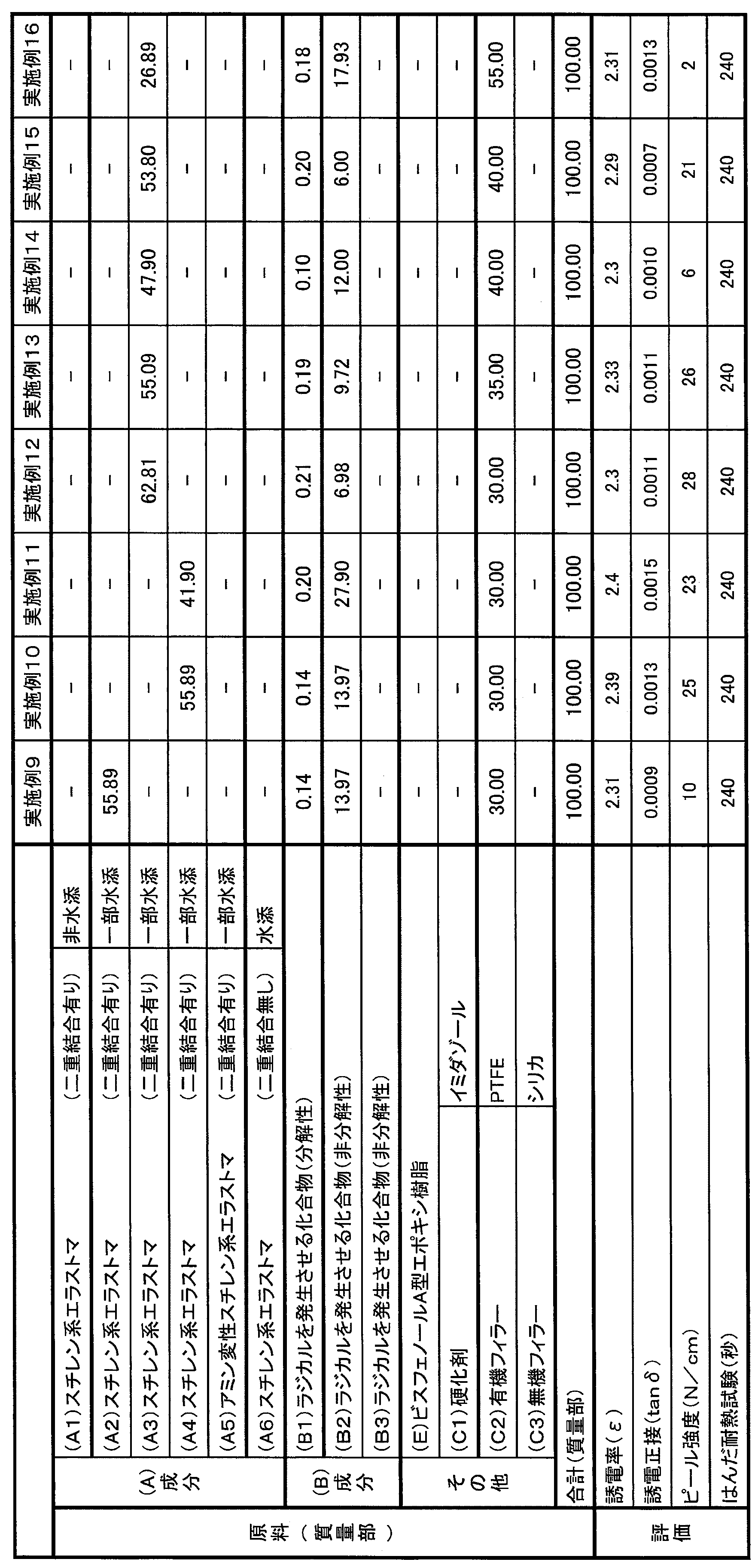
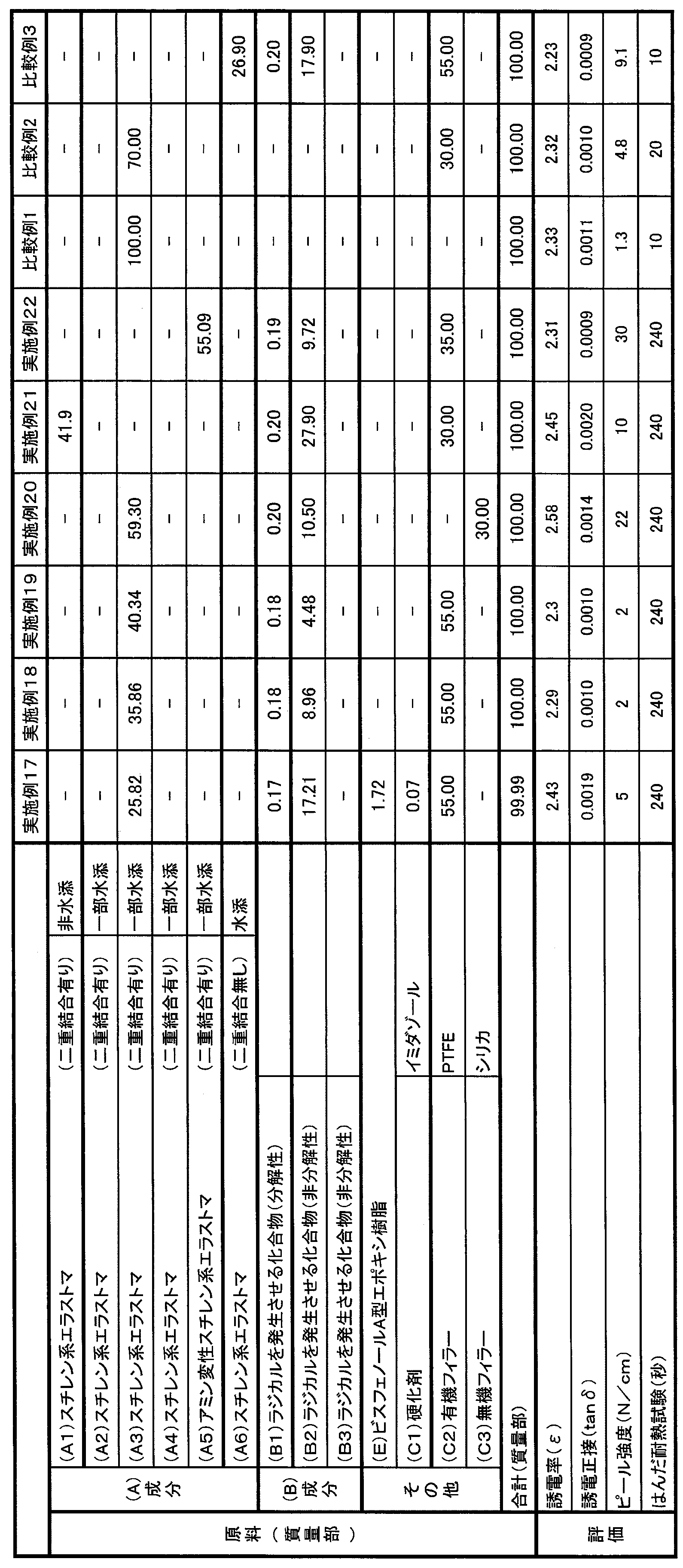
表1~表3に示すように、(A)成分として二重結合を有するスチレン系エラストマと、(B)成分としてラジカルを発生させる化合物とを含む樹脂組成物の硬化物は、誘電率(ε)及び誘電正接(tanδ)について良好な値を示すものであった。また、このような硬化物は、ピール強度及びはんだ耐熱試験についても良好な結果となった。
一方で、比較例1の樹脂組成物は、(B)成分としてラジカルを発生させる化合物を含んでいないため、ピール強度及びはんだ耐熱試験の評価結果が非常に劣るものであった。比較例2の樹脂組成物は、一定量の有機フィラー((C2)PTFE)を含んでいるものの、(B)成分としてラジカルを発生させる化合物を含んでいないため、はんだ耐熱試験の評価結果が非常に劣るものであった。比較例3の樹脂組成物は、(A)成分として二重結合を有さないスチレン系エラストマを用いた樹脂組成物であり、ピール強度には優れるものの、はんだ耐熱試験の評価結果が非常に劣るものであった。
本発明のアンテナ付き半導体パッケージは、5Gミリ波の送信・受信の通信を行うRFチップが実装される高周波基板として利用することができる。本発明のアンテナ付き半導体パッケージ用樹脂組成物は、本発明のアンテナ付き半導体パッケージの絶縁層に利用することができる。
1 絶縁層
1A 第一絶縁層
1B 第二絶縁層
1C 第三絶縁層
1D 第四絶縁層
1E 第五絶縁層
2 コア基板
4 配線層
5 アンテナ部(パッチアンテナ)
7 電気連結金属
8 RFチップ
9 接続パッド
10 半導体装置部
21 絶縁層
22 コア基板
24 配線層
25 アンテナ部(パッチアンテナ)
26 アンテナ部(ダイポールアンテナ)
27 電気連結金属
28 RFチップ
30 半導体装置部
100,200 アンテナ付き半導体パッケージ
1A 第一絶縁層
1B 第二絶縁層
1C 第三絶縁層
1D 第四絶縁層
1E 第五絶縁層
2 コア基板
4 配線層
5 アンテナ部(パッチアンテナ)
7 電気連結金属
8 RFチップ
9 接続パッド
10 半導体装置部
21 絶縁層
22 コア基板
24 配線層
25 アンテナ部(パッチアンテナ)
26 アンテナ部(ダイポールアンテナ)
27 電気連結金属
28 RFチップ
30 半導体装置部
100,200 アンテナ付き半導体パッケージ
Claims (9)
- 半導体装置部にアンテナ部が一体的に形成されたアンテナ付き半導体パッケージであって、
前記半導体装置部と前記アンテナ部とを接続するための絶縁層、及び前記アンテナ部内部の絶縁層のうちの少なくとも一方が、
(A)二重結合を有するスチレン系エラストマと、(B)ラジカルを発生させる化合物とを含む樹脂組成物の硬化物である、アンテナ付き半導体パッケージ。 - 前記硬化物中のエポキシ樹脂及び硬化剤の合計質量が、前記(A)二重結合を有するスチレン系エラストマ及び前記(B)ラジカルを発生させる化合物の合計100質量部に対して、5質量部以下である、請求項1に記載のアンテナ付き半導体パッケージ。
- 前記(A)二重結合を有するスチレン系エラストマが、スチレン/ブタジエン/ブチレン/スチレンブロックコポリマーを含む、請求項1又は2記載のアンテナ付き半導体パッケージ。
- 前記硬化物がPTFEフィラーを含む、請求項1~3のいずれか一項に記載のアンテナ付き半導体パッケージ。
- (A)二重結合を有するスチレン系エラストマと、(B)ラジカルを発生させる化合物とを含む、アンテナ付き半導体パッケージ用樹脂組成物。
- 樹脂組成物中のエポキシ樹脂及び硬化剤の合計質量が、前記(A)二重結合を有するスチレン系エラストマ及び前記(B)ラジカルを発生させる化合物の合計100質量部に対して、5質量部以下である、請求項5に記載のアンテナ付き半導体パッケージ用樹脂組成物。
- 前記(A)二重結合を有するスチレン系エラストマが、スチレン/ブタジエン/ブチレン/スチレンブロックコポリマーを含む、請求項5又は6記載のアンテナ付き半導体パッケージ用樹脂組成物。
- PTFEフィラーを含む、請求項5~7のいずれか一項に記載のアンテナ付き半導体パッケージ用樹脂組成物。
- 請求項5~8のいずれか一項に記載の樹脂組成物を含むアンテナ付き半導体パッケージ用フィルム。
Priority Applications (5)
| Application Number | Priority Date | Filing Date | Title |
|---|---|---|---|
| JP2022533847A JP7630847B2 (ja) | 2020-07-03 | 2021-06-17 | アンテナ付き半導体パッケージ及びアンテナ付き半導体パッケージ用樹脂組成物 |
| US18/010,265 US20230299461A1 (en) | 2020-07-03 | 2021-06-17 | Antenna-equipped semiconductor package and resin composition for antenna-equipped semiconductor package |
| KR1020237000117A KR102912082B1 (ko) | 2020-07-03 | 2021-06-17 | 안테나 부착 반도체 패키지 및 안테나 부착 반도체 패키지용 수지 조성물 |
| CN202180047205.3A CN115812249A (zh) | 2020-07-03 | 2021-06-17 | 带天线的半导体封装体和带天线的半导体封装体用树脂组合物 |
| JP2024201389A JP2025015763A (ja) | 2020-07-03 | 2024-11-19 | アンテナ付き半導体パッケージ及びアンテナ付き半導体パッケージ用樹脂組成物 |
Applications Claiming Priority (2)
| Application Number | Priority Date | Filing Date | Title |
|---|---|---|---|
| JP2020115697 | 2020-07-03 | ||
| JP2020-115697 | 2020-07-03 |
Publications (1)
| Publication Number | Publication Date |
|---|---|
| WO2022004409A1 true WO2022004409A1 (ja) | 2022-01-06 |
Family
ID=79316066
Family Applications (1)
| Application Number | Title | Priority Date | Filing Date |
|---|---|---|---|
| PCT/JP2021/023019 Ceased WO2022004409A1 (ja) | 2020-07-03 | 2021-06-17 | アンテナ付き半導体パッケージ及びアンテナ付き半導体パッケージ用樹脂組成物 |
Country Status (6)
| Country | Link |
|---|---|
| US (1) | US20230299461A1 (ja) |
| JP (2) | JP7630847B2 (ja) |
| KR (1) | KR102912082B1 (ja) |
| CN (1) | CN115812249A (ja) |
| TW (1) | TWI905217B (ja) |
| WO (1) | WO2022004409A1 (ja) |
Cited By (2)
| Publication number | Priority date | Publication date | Assignee | Title |
|---|---|---|---|---|
| WO2022177006A1 (ja) * | 2021-02-22 | 2022-08-25 | 昭和電工マテリアルズ株式会社 | 樹脂組成物、硬化物、積層体、透明アンテナ及びその製造方法、並びに、画像表示装置 |
| WO2024098356A1 (en) * | 2022-11-11 | 2024-05-16 | Innoscience (suzhou) Semiconductor Co., Ltd. | Nitride-based semiconductor circuit and method for manufacturing thereof |
Families Citing this family (2)
| Publication number | Priority date | Publication date | Assignee | Title |
|---|---|---|---|---|
| US12266618B2 (en) * | 2022-02-18 | 2025-04-01 | Advanced Semiconductor Engineering, Inc. | Semiconductor device and method of manufacturing the same |
| US12597706B2 (en) | 2022-04-08 | 2026-04-07 | Advanced Semiconductor Engineering, Inc. | Electronic device antenna package with multiple antennas |
Citations (1)
| Publication number | Priority date | Publication date | Assignee | Title |
|---|---|---|---|---|
| WO2018016489A1 (ja) * | 2016-07-19 | 2018-01-25 | 日立化成株式会社 | 樹脂組成物、積層板及び多層プリント配線板 |
Family Cites Families (21)
| Publication number | Priority date | Publication date | Assignee | Title |
|---|---|---|---|---|
| JP4394266B2 (ja) * | 2000-09-18 | 2010-01-06 | カシオ計算機株式会社 | 半導体装置および半導体装置の製造方法 |
| CN101819648A (zh) * | 2004-10-13 | 2010-09-01 | 凸版资讯股份有限公司 | 非接触ic标签及其制造方法和制造装置 |
| JP2006113750A (ja) * | 2004-10-13 | 2006-04-27 | Toppan Forms Co Ltd | 非接触型データ受送信体 |
| JP2006253953A (ja) * | 2005-03-09 | 2006-09-21 | Fujitsu Ltd | 通信用高周波モジュールおよびその製造方法 |
| JP4101814B2 (ja) * | 2005-03-15 | 2008-06-18 | 富士通株式会社 | 高周波モジュール |
| JP4732128B2 (ja) * | 2005-11-01 | 2011-07-27 | 太陽誘電株式会社 | 高周波無線モジュール |
| JP5303852B2 (ja) * | 2006-04-13 | 2013-10-02 | 日立化成株式会社 | セミipn型複合体の樹脂組成物並びにこれを用いたワニス、プリプレグ及び金属張積層板 |
| JP5435685B2 (ja) * | 2007-02-28 | 2014-03-05 | ナミックス株式会社 | 封止用樹脂フィルム |
| JP5435699B2 (ja) * | 2009-03-06 | 2014-03-05 | ナミックス株式会社 | 配線基板の製造方法、配線基板および半導体装置 |
| JP5731148B2 (ja) * | 2010-09-03 | 2015-06-10 | ナミックス株式会社 | フィルムアンテナおよびその製造方法、ならびに、それに用いるアンテナ基板用フィルム |
| KR20140009201A (ko) * | 2011-01-07 | 2014-01-22 | 가부시끼가이샤 다이셀 | 경화성 에폭시 수지 조성물 |
| CN103140089A (zh) * | 2011-12-05 | 2013-06-05 | 深圳富泰宏精密工业有限公司 | 壳体的制备方法及由该方法制得的壳体 |
| JP5726787B2 (ja) * | 2012-02-28 | 2015-06-03 | 株式会社東芝 | 無線装置、それを備えた情報処理装置および記憶装置 |
| JP6031059B2 (ja) * | 2014-03-31 | 2016-11-24 | 信越化学工業株式会社 | 半導体装置、積層型半導体装置、封止後積層型半導体装置、及びこれらの製造方法 |
| KR20170122722A (ko) * | 2014-12-25 | 2017-11-06 | 리켄 테크노스 가부시키가이샤 | 전지 팩 보호 부재용 열가소성 엘라스토머 조성물 |
| JP6570259B2 (ja) * | 2015-02-11 | 2019-09-04 | ナミックス株式会社 | 樹脂組成物、絶縁フィルム、および半導体装置 |
| JP6682190B2 (ja) * | 2015-04-17 | 2020-04-15 | ナミックス株式会社 | 金属被膜付絶縁体、半導体装置、および金属被膜付絶縁体の製造方法 |
| US20200058577A1 (en) * | 2017-02-22 | 2020-02-20 | Namics Corporation | Multi-layer wiring substrate and semiconductor device |
| KR102460870B1 (ko) * | 2017-10-20 | 2022-10-31 | 삼성전기주식회사 | 인쇄회로기판 |
| JP7020332B2 (ja) * | 2018-07-26 | 2022-02-16 | 味の素株式会社 | 樹脂組成物 |
| KR102426215B1 (ko) * | 2018-12-04 | 2022-07-28 | 삼성전기주식회사 | 인쇄회로기판 및 이를 포함하는 모듈 |
-
2021
- 2021-06-17 US US18/010,265 patent/US20230299461A1/en active Pending
- 2021-06-17 CN CN202180047205.3A patent/CN115812249A/zh active Pending
- 2021-06-17 KR KR1020237000117A patent/KR102912082B1/ko active Active
- 2021-06-17 WO PCT/JP2021/023019 patent/WO2022004409A1/ja not_active Ceased
- 2021-06-17 JP JP2022533847A patent/JP7630847B2/ja active Active
- 2021-06-29 TW TW110123749A patent/TWI905217B/zh active
-
2024
- 2024-11-19 JP JP2024201389A patent/JP2025015763A/ja active Pending
Patent Citations (1)
| Publication number | Priority date | Publication date | Assignee | Title |
|---|---|---|---|---|
| WO2018016489A1 (ja) * | 2016-07-19 | 2018-01-25 | 日立化成株式会社 | 樹脂組成物、積層板及び多層プリント配線板 |
Cited By (2)
| Publication number | Priority date | Publication date | Assignee | Title |
|---|---|---|---|---|
| WO2022177006A1 (ja) * | 2021-02-22 | 2022-08-25 | 昭和電工マテリアルズ株式会社 | 樹脂組成物、硬化物、積層体、透明アンテナ及びその製造方法、並びに、画像表示装置 |
| WO2024098356A1 (en) * | 2022-11-11 | 2024-05-16 | Innoscience (suzhou) Semiconductor Co., Ltd. | Nitride-based semiconductor circuit and method for manufacturing thereof |
Also Published As
| Publication number | Publication date |
|---|---|
| JPWO2022004409A1 (ja) | 2022-01-06 |
| TW202220119A (zh) | 2022-05-16 |
| US20230299461A1 (en) | 2023-09-21 |
| TWI905217B (zh) | 2025-11-21 |
| KR102912082B1 (ko) | 2026-01-13 |
| JP2025015763A (ja) | 2025-01-30 |
| CN115812249A (zh) | 2023-03-17 |
| KR20230035029A (ko) | 2023-03-10 |
| JP7630847B2 (ja) | 2025-02-18 |
Similar Documents
| Publication | Publication Date | Title |
|---|---|---|
| JP7630847B2 (ja) | アンテナ付き半導体パッケージ及びアンテナ付き半導体パッケージ用樹脂組成物 | |
| JP7378494B2 (ja) | 共重合体及びこれを含む積層体 | |
| JP7428815B2 (ja) | 組成物及びその硬化体 | |
| KR102323672B1 (ko) | 수지 조성물 및 이를 사용한 절연 필름 및 반도체 장치 | |
| JP4325337B2 (ja) | 樹脂組成物、それを用いたプリプレグ、積層板及び多層プリント配線板 | |
| KR101116181B1 (ko) | 성형성이 우수한 에폭시수지를 포함한 적층체 및 그 제조방법 | |
| JP6136348B2 (ja) | 多層伝送線路板、該多層伝送線路板を有する電磁結合モジュール、アンテナモジュール | |
| TW202313831A (zh) | 樹脂組成物及其製造方法以及接著薄膜及層間接著用黏合片 | |
| TW201910123A (zh) | 銅箔基板和包含它的印刷電路板 | |
| WO2005100435A1 (ja) | エポキシ樹脂組成物 | |
| KR101797723B1 (ko) | 접착용 수지 조성물, 접착용 필름 및 연성 금속 적층체 | |
| KR20240072288A (ko) | 수지 시트, 적층판, 금속 피복 적층판, 프린트 배선판 및 반도체 패키지 | |
| Sato et al. | High performance insulating adhesive film for high-frequency applications | |
| KR20250055502A (ko) | 수지 조성물, 접착 필름, 층간 접착용 본딩 시트, 및 안테나가 형성된 반도체 패키지용 수지 조성물 | |
| JP7513467B2 (ja) | グラフト変性ポリメチルペンテン組成物、成形品、及び銅張積層板 | |
| JP7569954B1 (ja) | 熱硬化性接着剤組成物、熱硬化性接着シート及びプリント配線板 | |
| WO2023053749A1 (ja) | 樹脂組成物、接着フィルム、層間接着用ボンディングシート、アンテナ付き半導体パッケージ用樹脂組成物及びアンテナ付き半導体パッケージ | |
| JP2023013224A (ja) | アンテナモジュール用積層板の製造方法、アンテナ装置の製造方法、アンテナモジュールの製造方法及び通信装置の製造方法 | |
| JP2003060359A (ja) | 多層回路基板 | |
| TWI843644B (zh) | 樹脂組合物 | |
| US20250066609A1 (en) | Resin composition | |
| TW202423200A (zh) | 電路基板之製造方法 | |
| WO2025187225A1 (ja) | 接着層用フィルム、配線基板、多層配線基板、及び半導体装置。 | |
| CN117777663A (zh) | 一种树脂组合物及其应用 | |
| CN118202522A (zh) | 用于低成本pcb mmwave相控阵天线的双背钻过孔 |
Legal Events
| Date | Code | Title | Description |
|---|---|---|---|
| 121 | Ep: the epo has been informed by wipo that ep was designated in this application |
Ref document number: 21833015 Country of ref document: EP Kind code of ref document: A1 |
|
| ENP | Entry into the national phase |
Ref document number: 2022533847 Country of ref document: JP Kind code of ref document: A |
|
| NENP | Non-entry into the national phase |
Ref country code: DE |
|
| 122 | Ep: pct application non-entry in european phase |
Ref document number: 21833015 Country of ref document: EP Kind code of ref document: A1 |