WO2021214932A1 - 半導体装置およびその製造方法 - Google Patents
半導体装置およびその製造方法 Download PDFInfo
- Publication number
- WO2021214932A1 WO2021214932A1 PCT/JP2020/017453 JP2020017453W WO2021214932A1 WO 2021214932 A1 WO2021214932 A1 WO 2021214932A1 JP 2020017453 W JP2020017453 W JP 2020017453W WO 2021214932 A1 WO2021214932 A1 WO 2021214932A1
- Authority
- WO
- WIPO (PCT)
- Prior art keywords
- layer
- electrode
- gan
- emitter
- algan
- Prior art date
- Legal status (The legal status is an assumption and is not a legal conclusion. Google has not performed a legal analysis and makes no representation as to the accuracy of the status listed.)
- Ceased
Links
Images








Classifications
-
- H—ELECTRICITY
- H10—SEMICONDUCTOR DEVICES; ELECTRIC SOLID-STATE DEVICES NOT OTHERWISE PROVIDED FOR
- H10D—INORGANIC ELECTRIC SEMICONDUCTOR DEVICES
- H10D10/00—Bipolar junction transistors [BJT]
- H10D10/80—Heterojunction BJTs
- H10D10/821—Vertical heterojunction BJTs
- H10D10/841—Vertical heterojunction BJTs having a two-dimensional base, e.g. modulation-doped base, inversion layer base or delta-doped base
-
- H—ELECTRICITY
- H10—SEMICONDUCTOR DEVICES; ELECTRIC SOLID-STATE DEVICES NOT OTHERWISE PROVIDED FOR
- H10D—INORGANIC ELECTRIC SEMICONDUCTOR DEVICES
- H10D30/00—Field-effect transistors [FET]
- H10D30/01—Manufacture or treatment
- H10D30/015—Manufacture or treatment of FETs having heterojunction interface channels or heterojunction gate electrodes, e.g. HEMT
-
- H—ELECTRICITY
- H10—SEMICONDUCTOR DEVICES; ELECTRIC SOLID-STATE DEVICES NOT OTHERWISE PROVIDED FOR
- H10D—INORGANIC ELECTRIC SEMICONDUCTOR DEVICES
- H10D10/00—Bipolar junction transistors [BJT]
- H10D10/01—Manufacture or treatment
- H10D10/021—Manufacture or treatment of heterojunction BJTs [HBT]
-
- H—ELECTRICITY
- H10—SEMICONDUCTOR DEVICES; ELECTRIC SOLID-STATE DEVICES NOT OTHERWISE PROVIDED FOR
- H10D—INORGANIC ELECTRIC SEMICONDUCTOR DEVICES
- H10D30/00—Field-effect transistors [FET]
- H10D30/40—FETs having zero-dimensional [0D], one-dimensional [1D] or two-dimensional [2D] charge carrier gas channels
- H10D30/47—FETs having zero-dimensional [0D], one-dimensional [1D] or two-dimensional [2D] charge carrier gas channels having two-dimensional [2D] charge carrier gas channels, e.g. nanoribbon FETs or high electron mobility transistors [HEMT]
- H10D30/471—High electron mobility transistors [HEMT] or high hole mobility transistors [HHMT]
- H10D30/475—High electron mobility transistors [HEMT] or high hole mobility transistors [HHMT] having wider bandgap layer formed on top of lower bandgap active layer, e.g. undoped barrier HEMTs such as i-AlGaN/GaN HEMTs
-
- H—ELECTRICITY
- H10—SEMICONDUCTOR DEVICES; ELECTRIC SOLID-STATE DEVICES NOT OTHERWISE PROVIDED FOR
- H10D—INORGANIC ELECTRIC SEMICONDUCTOR DEVICES
- H10D62/00—Semiconductor bodies, or regions thereof, of devices having potential barriers
- H10D62/80—Semiconductor bodies, or regions thereof, of devices having potential barriers characterised by the materials
- H10D62/85—Semiconductor bodies, or regions thereof, of devices having potential barriers characterised by the materials being Group III-V materials, e.g. GaAs
- H10D62/8503—Nitride Group III-V materials, e.g. AlN or GaN
Definitions
- the present invention relates to a semiconductor device composed of a nitride semiconductor and a method for manufacturing the same.
- Gallium nitride (GaN) -based materials are promising as high-voltage power devices and high-power high-frequency device materials because they have a large bandgap and high dielectric breakdown electric field strength.
- GaN has a hexagonal wurtzite structure as a stable phase, and polarization occurs in the c-axis direction. By utilizing this effect, a high-concentration two-dimensional electron gas can be formed at the AlGaN / GaN interface.
- High electron mobility transistors (HEMTs) using this two-dimensional electron gas have been actively studied.
- a heterojunction bipolar transistor which is a vertical element using a nitride semiconductor, has a feature that the current density and power density can be higher than those of HEMT, so that it can be used for high frequency and power applications. Is expected to be applied.
- high-performance devices not only for transistors but also for 2-terminal elements such as Schottky barrier diodes and pn junction diodes.
- GaN HEMT In the application of GaN HEMT as a power device, a so-called normal off operation in which the transistor is turned off when the power is off is desired from the viewpoint of compensating for the operation of the electronic circuit.
- a GIT Gate Injection Transistor
- the p-GaN layer is formed on the AlGaN barrier layer in the gate region to raise the energy of the conduction band and realize the normalization operation.
- the GIT structure can be formed without including the recess etching process of the AlGaN barrier layer, so that it is excellent in controllability and productivity, and the device can be manufactured only with GaN-based materials.
- a high-performance device can be manufactured using a GaN substrate or the like.
- the p-type layer is also very useful in the GaN MOSFET structure.
- it may be used for so-called current constriction in which a current is concentrated in a region directly under the gate by forming a pn junction by a p-type region formed directly under the channel region. .. It is also possible to separate elements by pn junction.
- the base layer requires a GaN-based material in which a high concentration of p-type impurities is doped.
- the importance of controlling the p-type layer is increasing in order to improve the performance of GaN devices.
- the technique of forming ohmic contact with the electrode is a very important technique not only in the actual device but also in the process of evaluating the crystal quality of, for example, the p-type GaN layer.
- a low-resistance ohmic electrode forming technique for p-type GaN has not yet been realized.
- NiO formed by oxidation of a Ni electrode by an annealing treatment in an atmosphere such as air is a factor capable of reducing contact resistance.
- a sufficiently low contact resistance cannot be obtained.
- One of the techniques for increasing the hole concentration in GaN-based materials is a method using two-dimensional hole gas.
- the AlGaN / GaN interface With the polarization axis reversed from that of the conventional HEMT, the bending of the band of the valence band toward the Fermi level is formed at the AlGaN / GaN interface.
- Dimensional hole gas can be generated. It is considered that this structure capable of obtaining a high hole concentration by utilizing such a polarization effect in a nitride semiconductor can be applied to various devices (Non-Patent Document 1).
- the structure using the AlGaN / GaN interface in which the polarization axis is reversed described above has difficulty in forming an ohmic electrode.
- two-dimensional hole gas is generated directly under the AlGaN layer, and this is generated at the hetero interface due to the effect of polarization of AlGaN and GaN.
- AlGaN is a high resistance material, forming an electrode through AlGaN can hinder the reduction of contact resistance.
- the AlGaN layer is recess-etched to form a direct contact with GaN, the two-dimensional hole gas disappears directly under the recess-etched AlGaN layer, and the effect of the two-dimensional hole gas is sufficient. It cannot be used (Non-Patent Document 2).
- p-type GaN is important in GaN devices, but GaN cannot increase the hole concentration. Therefore, it is difficult to form an electrode on p-type GaN with a low contact resistance, and its application as a device is limited. Further, in the technique of forming a two-dimensional hole gas with the N-polar plane as the main plane orientation to increase the hole concentration, it is difficult to realize a low contact resistance because the resistance of the AlGaN layer serving as a barrier is high. ..
- the present invention has been made to solve the above problems, and an object of the present invention is to reduce the contact resistance to the two-dimensional hole gas formed near the heterojunction interface between GaN and AlGaN. ..
- the semiconductor device has a first semiconductor layer made of p-type GaN formed on a substrate with the main surface set to N polarity, and a main surface N on the first semiconductor layer.
- the second semiconductor layer made of undoped AlGaN formed in a polar state, the electrode made of an electrode material containing Ni formed on the second semiconductor layer, and the second semiconductor layer and the electrode are in contact with each other. It is provided with an oxide layer made of an oxide of an electrode material formed between the second semiconductor layer and the electrode.
- the method for manufacturing a semiconductor device is a first step of forming a first semiconductor layer made of p-type GaN on a substrate with the main surface set to N polarity, and on the first semiconductor layer.
- a fifth step is provided in which the oxide layer is formed, and the oxide layer is arranged between the electrode and the second semiconductor layer in a state of being in contact with both the second semiconductor layer and the electrode.
- the semiconductor device is formed on a substrate with a collector layer made of GaN in which the main surface is N-polar, and on the collector layer in a state where the main surface is N-polar.
- the method for manufacturing a semiconductor device includes a first step of forming a collector layer made of GaN on a substrate with the main surface set to N polarity, and a method of forming a collector layer made of GaN on the collector layer with the main surface set to N polarity.
- the sixth step of forming the base electrode composed of the above in contact with the surface oxide layer and by heating, an oxide layer made of the oxide of the electrode material is formed in the portion of the base electrode in contact with the surface oxide layer. Then, between the base electrode and the emitter layer, the seventh step of arranging the oxide layer in a state of being in contact with both the emitter layer and the base electrode, and the collector electrode electrically connected to the collector layer are provided. It includes an eighth step of forming.
- the second semiconductor layer (emitter layer) and the electrode (base electrode) are in contact with both the second semiconductor layer (emitter layer) and the electrode (base layer) made of AlGaN. Since the oxide layer made of the oxide of the electrode material formed between them is provided, the contact resistance to the two-dimensional hole gas formed in the vicinity of the heterojunction interface between GaN and AlGaN can be lowered.
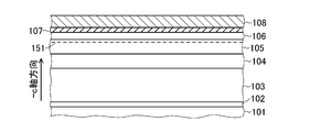
- FIG. 1A is a cross-sectional view showing a state of a semiconductor device in an intermediate process for explaining a method for manufacturing a semiconductor device according to the first embodiment of the present invention.
- FIG. 1B is a cross-sectional view showing a state of the semiconductor device in the intermediate process for explaining the method for manufacturing the semiconductor device according to the first embodiment of the present invention.
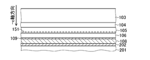
- FIG. 1C is a cross-sectional view showing a state of the semiconductor device in the intermediate process for explaining the manufacturing method of the semiconductor device according to the first embodiment of the present invention.
- FIG. 1D is a cross-sectional view showing a state of the semiconductor device in the intermediate process for explaining the manufacturing method of the semiconductor device according to the first embodiment of the present invention.
- FIG. 1A is a cross-sectional view showing a state of a semiconductor device in an intermediate process for explaining a method for manufacturing a semiconductor device according to the first embodiment of the present invention.
- FIG. 1B is a cross-sectional view showing a state of the semiconductor device in the intermediate
- FIG. 2 is a cross-sectional view showing the configuration of another semiconductor device according to the first embodiment of the present invention.
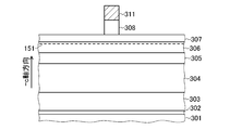
- FIG. 3A is a cross-sectional view showing a state of the semiconductor device in the intermediate process for explaining the manufacturing method of the semiconductor device according to the first embodiment of the present invention.
- FIG. 3B is a cross-sectional view showing a state of the semiconductor device in the intermediate process for explaining the manufacturing method of the semiconductor device according to the first embodiment of the present invention.
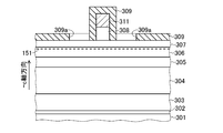
- FIG. 3C is a cross-sectional view showing a state of the semiconductor device in the intermediate process for explaining the manufacturing method of the semiconductor device according to the first embodiment of the present invention.
- FIG. 3A is a cross-sectional view showing a state of the semiconductor device in the intermediate process for explaining the manufacturing method of the semiconductor device according to the first embodiment of the present invention.
- FIG. 3B is a cross-sectional view showing a state of the semiconductor device in the intermediate process for explaining the manufacturing method of the semiconductor device according to the first embodiment of the present invention.
- FIG. 3D is a cross-sectional view showing a state of the semiconductor device in the intermediate process for explaining the manufacturing method of the semiconductor device according to the first embodiment of the present invention.
- FIG. 3E is a cross-sectional view showing a state of the semiconductor device in the intermediate process for explaining the manufacturing method of the semiconductor device according to the first embodiment of the present invention.
- FIG. 3F is a cross-sectional view showing a state of the semiconductor device in the intermediate process for explaining the manufacturing method of the semiconductor device according to the first embodiment of the present invention.
- FIG. 3G is a cross-sectional view showing a state of the semiconductor device in the intermediate process for explaining the manufacturing method of the semiconductor device according to the first embodiment of the present invention.
- FIG. 3H is a cross-sectional view showing a state of the semiconductor device in the intermediate process for explaining the manufacturing method of the semiconductor device according to the first embodiment of the present invention.
- FIG. 4A is a cross-sectional view showing a state of the semiconductor device in the intermediate process for explaining the manufacturing method of the semiconductor device according to the first embodiment of the present invention.
- FIG. 4B is a cross-sectional view showing a state of the semiconductor device in the intermediate process for explaining the manufacturing method of the semiconductor device according to the first embodiment of the present invention.
- FIG. 4C is a cross-sectional view showing a state of the semiconductor device in the intermediate process for explaining the manufacturing method of the semiconductor device according to the first embodiment of the present invention.
- FIG. 4D is a cross-sectional view showing a state of the semiconductor device in the intermediate process for explaining the manufacturing method of the semiconductor device according to the first embodiment of the present invention.
- the nucleation layer 102, the buffer layer 103, the p-GaN layer 104, the i-GaN layer 105, and the i-AlGaN layer 106 were placed on the substrate 101 with the main surface set to N polarity. In this state (in the ⁇ c axis direction), epitaxial growth is carried out in these order (first step, second step).
- the substrate 101 is made of, for example, Al 2 O 3 (sapphire), and the plane orientation of the main surface is, for example, (0001).
- the substrate 101 can be made of a material capable of crystal growth of nitride semiconductors such as GaN, AlGaN, and InGaN, and whose main plane orientation can be an N-polar plane.
- the nucleation layer 102 is made of, for example, GaN. As is well known, the nucleation layer 102 supports nucleation in the early stage of growth in order to crystallize a nitride semiconductor such as GaN on a dissimilar substrate such as Al 2 O 3, and is of high quality. This is a layer for obtaining flat crystals.
- the nucleation layer 102 has various names such as a low temperature buffer layer and a low temperature buffer. Further, by adjusting the nucleation layer 102, the surface of the nucleation layer 102 becomes a group V polar (N polar) surface.
- a nitride semiconductor can grow crystals on the nucleation layer 102 in the ⁇ c axis direction.
- the nucleation layer 102 is not limited to GaN, and can be composed of other nitrides such as AlN and AlON. However, when the substrate 101 is made of GaN, the nucleation layer 102 may not be necessary.
- the buffer layer 103 is composed of GaN
- the p-GaN layer 104 is composed of p-type GaN
- the i-GaN layer 105 is composed of undoped GaN
- the i-AlGaN layer 106 is composed of undoped AlGaN.
- Each of these semiconductor layers can be formed by the well-known metalorganic vapor phase growth method. Further, each of the above-mentioned semiconductor layers can be formed (epitaxially grown) by molecular beam epitaxy (there is a classification such as gas source, RF plasma source, laser, etc., but any of them may be used), a hydride vapor phase growth method, or the like.
- each layer is crystal-grown on a growth substrate in advance with Group III polarity (Ga polarity).
- the i-AlGaN layer 106, the i-GaN layer 105, and the p-GaN layer 104 are laminated in this order on the growth substrate from the growth substrate side. This can also be formed by bonding this to another substrate by wafer bonding and then removing the growth substrate. When the growth substrate is removed by bonding to another substrate, each layer is laminated on the other substrate with the main surface having N polarity (in the ⁇ c axis direction). Further, the p-GaN layer 104, the i-GaN layer 105, and the i-AlGaN layer 106 are laminated in this order on another substrate.
- the selection of the buffer layer for growing the i-AlGaN layer 106, the i-GaN layer 105, and the p-GaN layer 104 on the growth substrate is also different. It will be appropriately selected so that the group III polar plane is the main plane orientation.
- the plane orientation at the time of crystal growth is not important, and the p-GaN layer 104, the i-GaN layer 105, and the i-AlGaN layer 106 are laminated in this order with the main surface having N polarity. It is important that it is done.
- a two-dimensional hole gas 151 is generated in the vicinity of the heterojunction interface formed by the i-AlGaN layer 106, and a high hole concentration can be obtained.
- the surface of the i-AlGaN layer 106 is oxidized to form the surface oxide layer 107 made of AlGaON as shown in FIG. 1B (third step).
- the surface of the i-AlGaN layer 106 can be oxidized.
- the surface of the i-AlGaN layer 106 can be oxidized by heating in an atmosphere of air or oxygen. Since AlGaN contains Al, it is more easily oxidized than GaN.
- an electrode 108 made of an electrode material containing Ni is formed in contact with the surface oxide layer 107 (fourth step).
- the electrode 108 can be formed by depositing Ni by using, for example, electron beam deposition or a sputtering method.
- an oxide layer 109 made of an oxide of the electrode 108 material is formed at a portion of the electrode 108 in contact with the surface oxide layer 107 (fifth step).
- the oxide layer 109 is arranged between the electrode 108 and the i-AlGaN layer 106 in a state of being in contact with both the i-AlGaN layer 106 and the electrode 108.
- NiO is easily p-typed and efficiently forms ohmic contact with the two-dimensional hole gas 151.
- the temperature and time of the heat treatment are set to an appropriate temperature and time at which ohmic contact (ohmic contact) between the oxide layer 109 and the two-dimensional hole gas 151 can be obtained.
- the main surface is formed on the substrate 101 with the main surface set to N polarity, and the main surface is formed on the p-GaN layer 104 made of p-type GaN and the p-GaN layer 104.
- An i-AlGaN layer 106 made of undoped AlGaN formed in an N-polar state, an electrode 108 made of an electrode 108 material containing Ni formed on the i-AlGaN layer 106, and an i-AlGaN layer 106.
- a semiconductor device including an oxide layer 109 made of an oxide of the electrode 108 material formed between the i-AlGaN layer 106 and the electrode 108 in contact with both the electrode 108 and the electrode 108 can be obtained.
- the oxide layer 109 is in ohmic contact with the two-dimensional hole gas formed in the vicinity of the interface of the p-GaN layer 104 with the i-AlGaN layer 106.
- the oxide layer 109 made of the oxide of the electrode material constituting the electrode 108 is provided (formed), the two-dimensional hole gas formed in the vicinity of the heterojunction interface between GaN and AlGaN is provided.
- the contact resistance to 151 can be lowered.
- the oxide layer 109 is formed by substituting a part of the surface oxide layer 107 with NiO. Further, the surface oxide layer 107 is composed of a part of the i-AlGaN layer 106. Therefore, by forming the oxide layer 109, the effective layer thickness of the i-AlGaN layer 106, which is a barrier layer, is reduced. The decrease in the effective layer thickness of the i-AlGaN layer 106 leads to a decrease in the concentration of the two-dimensional hole gas 151 immediately below the i-AlGaN layer 106. In order to suppress the decrease in the concentration of the two-dimensional hole gas 151 and obtain the above-mentioned ohmic contact, it is important to appropriately select each condition for forming the surface oxide layer 107.
- the surface of the substrate is designed to be an N-polar surface, but the present invention is not limited to this.
- each semiconductor layer is grown with the N-polar plane as the main plane orientation, the surface of the i-AlGaN layer 106 is oxidized to form the surface oxide layer 107, and the electrodes are formed. Form 108.
- the electrodes 108 of the substrate 101 are bonded onto the other substrate 201 via the adhesive metal layer 202 by wafer bonding, and the substrate 101 is removed to be placed on the other substrate 201.
- the main surface of each semiconductor layer can be laminated in a state of being group III polar.
- an appropriate material is selected from the viewpoint of wafer bonding.
- the adhesive metal layer 202 can be made of Au.
- the surface of the adhesive metal layer 202 may be impaired in surface flatness due to the heat treatment step for forming the oxide layer 109. In this case, the adhesive metal layer 202 is flattened by a technique such as chemical mechanical polishing.
- the electrode 108 is made of Ni, it may not be possible to use Ni alone from the viewpoint of adhesion to the semiconductor layer.
- the electrode 108 can be configured from a laminated structure in which Ti is deposited after Ni or Ni is deposited after Ti as long as the effect of the present invention is not impaired.
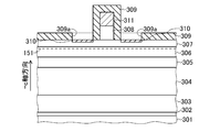
- a nucleation layer 302, a sub-collector layer 303, a collector layer 304, a p-base layer 305, an i-base layer 306, an emitter layer 307, and an emitter cap layer 308 are placed on the substrate 301.
- epitaxial growth is carried out in these order (first step, second step, third step).
- the substrate 301 is made of, for example, Al 2 O 3 (sapphire), and the plane orientation of the main surface is, for example, (0001).
- the substrate 301 can be made of a material capable of crystal growth of nitride semiconductors such as GaN, AlGaN, and InGaN, and whose main plane orientation can be an N-polar plane.
- the nucleation layer 302 is made of, for example, GaN. As is well known, the nucleation layer 302 supports nucleation in the early stage of growth in order to crystallize a nitride semiconductor such as GaN on a dissimilar substrate such as Al 2 O 3, and is of high quality. This is a layer for obtaining flat crystals.
- the nucleation layer 302 has various names such as a low temperature buffer layer and a low temperature buffer. Further, by adjusting the nucleation layer 302, the surface of the nucleation layer 302 becomes a group V polar (N polar) surface.
- a nitride semiconductor can grow crystals on the nucleation layer 302 in the ⁇ c axis direction.
- the nucleation layer 302 is not limited to GaN, and can be composed of other nitrides such as AlN and AlON. However, when the substrate 301 is made of GaN, the nucleation layer 302 may not be necessary.
- the sub-collector layer 303 is composed of n-type GaN. Since the sub-collector layer 303 needs to form ohmic contact with the collector electrode described later, it can be configured to be doped with a high concentration n-type. In addition, the sub-collector layer 303 can reduce the dislocation density as the layer thickness increases, and has the effect of improving crystal quality. Therefore, the sub-collector layer 303 can be formed to be relatively thick with a thickness of about several micrometers.
- the collector layer 304 is composed of undoped GaN.
- the collector layer 304 can also be composed of n-type GaN.
- the collector layer 304 is a layer that determines the withstand voltage of the heterojunction bipolar transistor, and determines the thickness and the doping concentration according to the specifications.
- the p-base layer 305 is composed of, for example, p-type GaN using Mg or the like as a dopant. Since the p-base layer 305 needs to form ohmic contact with the base electrode, which will be described later, it is desirable that the p-base layer 305 has a concentration as high as possible.
- the i-base layer 306 is composed of undoped GaN
- the emitter layer 307 is composed of undoped AlGaN.
- the interface between the i-base layer 306 and the emitter layer 307 is in a state where the band is bent by the spontaneous polarization and the piezoelectric polarization electric field, and the valence band end is above the Fermi level.
- the two-dimensional hole gas 151 is formed in the vicinity of the interface on the side of the i-base layer 306.
- the emitter cap layer 308 is composed of n-type AlGaN in which n-type impurities are introduced at a high concentration.
- Each of these semiconductor layers can be formed by the well-known metalorganic vapor phase growth method.
- each of the above-mentioned semiconductor layers can be formed (epitaxially grown) by molecular beam epitaxy (there is a classification such as gas source, RF plasma source, laser, etc., but any of them may be used), a hydride vapor phase growth method, or the like.
- the emitter electrode 311 is formed on the emitter layer 307 (fourth step).
- the emitter electrode 311 is formed on the emitter layer 307 via the emitter cap layer 308.
- an electrode material is deposited on the emitter cap layer 308 by a known deposition technique such as a sputtering method or a vapor deposition method to form a metal layer, and this metal layer is patterned by a known lithography technique and etching technique. Then, the emitter electrode 311 can be formed.
- an electrode material capable of forming ohmic contact with n-GaN constituting the emitter cap layer 308 is appropriately selected.
- the electrode material can be composed of a single material, for example, a laminated structure of materials such as Ni, Ti, Al, and Au that can form ohmic contact with n-GaN.
- an annealing treatment or the like may be performed to form an ohmic contact between the emitter electrode 311 and the emitter cap layer 308. Since the flatness of the electrode surface and the surface of the epitaxial wafer may be impaired by this annealing treatment, an appropriate protective film is deposited and the annealing treatment is performed.
- the emitter cap layer 308 is patterned into a mesa shape.
- the emitter electrode 311 is used as a mask and the emitter cap layer 308 is selectively etched by a known etching technique, the emitter cap layer 308 can be processed into a predetermined mesa shape (first mesa).
- a protective film 309 having an opening 309a is formed in the base electrode forming region.
- the surface of the emitter layer 307 exposed to the opening 309a around the emitter electrode 311 is oxidized to form a surface oxide layer 310 made of AlGaON (step 5).
- the surface oxide layer 310 can be formed by a technique of irradiating oxygen plasma or an annealing treatment in an air or oxygen atmosphere. Since AlGaN is more easily oxidized than GaN because it contains Al, the surface oxide layer 310 can be formed by the above-mentioned oxidation treatment.
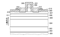
- a base electrode 312 composed of an electrode material containing Ni is formed in contact with the surface oxide layer 310 (sixth step).
- the base electrode 312 can be formed by depositing Ni by using, for example, electron beam deposition or a sputtering method.
- the device is heat-treated.
- an oxide layer made of an oxide (NiO) of the electrode material is formed on the portion of the base electrode 312 in contact with the surface oxide layer 310, and as shown in FIG. 3G, the base electrode 312 and the emitter layer 307 are combined.
- the oxide layer 321 is placed in contact with both the emitter layer 307 and the base electrode 312 (7th step).
- NiO is easily p-typed and efficiently forms ohmic contact with the two-dimensional hole gas 151.
- the temperature and time of the heat treatment are set to an appropriate temperature and time at which ohmic contact (ohmic contact) between the oxide layer 321 and the two-dimensional hole gas 151 can be obtained.
- the layer has a mesa shape.
- This mesa shape (second mesa) is, for example, rectangular in a plan view.
- the above-mentioned second mesa has a larger area in a plan view than the first mesa of the emitter cap layer 308.
- the collector electrode 313 is formed on the sub-collector layer 303 around the second mesa.
- the collector electrode 313 is electrically connected to the collector layer 304 via the sub-collector layer 303 (step 8).
- a heterojunction bipolar transistor including an oxide layer 321 formed between an emitter layer 307 and a base electrode 312 and made of an oxide of an electrode material, and a collector electrode 313 electrically connected to a collector layer 304. Device) is obtained.
- the oxide layer 321 is in ohmic contact with the two-dimensional hole gas formed in the vicinity of the interface of the p-base layer 305 with the emitter layer 307.
- the oxide layer 321 made of the oxide of the electrode material constituting the base electrode 312 is provided (formed), the two-dimensional holes formed in the vicinity of the heterojunction interface between GaN and AlGaN are provided.
- the contact resistance to the gas 151 can be lowered.
- the surface of the substrate is designed to have N polarity, but the present invention is not limited to this.
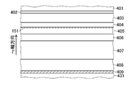
- the nucleation layer 402, the emitter cap layer 403, the emitter layer 404, the i-base layer 405, the p-base layer 406, the collector layer 407, and the sub-collector layer are placed on the growth substrate 401.
- 408 is epitaxially grown in this order with the main surface having a group III polarity (in the + c-axis direction).
- the growth substrate 401 is made of, for example, Al 2 O 3 (sapphire), and the plane orientation of the main surface is, for example, (0001).
- the growth substrate 401 can be made of a material capable of crystal growth of nitride semiconductors such as GaN, AlGaN, and InGaN, and whose main plane orientation can be an N-polar plane.
- the nucleation layer 402 is made of, for example, GaN.
- the emitter cap layer 403 is composed of n-type AlGaN in which n-type impurities are introduced at a high concentration.
- the emitter layer 404 is composed of undoped AlGaN, and the i-base layer 405 is composed of undoped GaN. With this configuration, the interface between the i-base layer 405 and the emitter layer 404 is in a state where the band is bent by the spontaneous polarization and the piezoelectric polarization electric field, and the valence band end is above the Fermi level. As a result, the two-dimensional hole gas 151 is formed in the vicinity of the interface on the side of the i-base layer 405.
- the p-base layer 406 is composed of p-type GaN.
- the collector layer 407 is composed of undoped GaN.
- the sub-collector layer 408 is composed of n-type GaN.
- Each of these semiconductor layers can be formed by the well-known metalorganic vapor phase growth method. Further, each of the above-mentioned semiconductor layers can be formed (epitaxially grown) by molecular beam epitaxy (there is a classification such as gas source, RF plasma source, laser, etc., but any of them may be used), a hydride vapor phase growth method, or the like. Further, a metal layer 409 made of metal is formed on the sub-collector layer 408.
- the metal layer 409 is used as an adhesive layer, and the heat dissipation substrate 431 having high heat dissipation is attached to the metal layer 409 by wafer bonding.
- the surface of the metal layer 409 can be flattened by a technique such as chemical mechanical polishing.
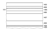
- the semiconductor layers are laminated (in the ⁇ c axis direction) with the main surface having N polarity.
- the nucleation layer 402 and the growth substrate 401 are removed to expose the surface of the emitter cap layer 403 as shown in FIG. 4C.
- the emitter electrode 411 is formed on the emitter layer 404, and the emitter cap layer 403 is formed into a mesa shape. Pattern.
- a base electrode 412 is formed on the emitter layer 404 via an oxide layer 421, and then an emitter layer 404, an i-base layer 405, a p-base layer 406, a collector layer 407, and a sub-collector layer are formed. By patterning the 408, these layers are formed into a mesa shape.
- the collector electrode 413 is formed on the metal layer 409 around the mesa. The collector electrode 413 is electrically connected to the collector layer 407 via the metal layer 409 and the sub-collector layer 408.
- the metal layer 409 can be used as a collector electrode, and a collector contact can be formed on the back surface side of the heat radiating substrate 431.
- the second semiconductor layer (emitter layer) and the electrode (base electrode) are in contact with both the second semiconductor layer (emitter layer) and the electrode (base layer) made of AlGaN. Since the oxide layer made of the oxide of the electrode material formed between the two is provided, the contact resistance to the two-dimensional hole gas formed in the vicinity of the heterojunction interface between GaN and AlGaN can be lowered.
Landscapes
- Bipolar Transistors (AREA)
- Electrodes Of Semiconductors (AREA)
Priority Applications (3)
| Application Number | Priority Date | Filing Date | Title |
|---|---|---|---|
| JP2022516570A JP7298779B2 (ja) | 2020-04-23 | 2020-04-23 | 半導体装置およびその製造方法 |
| US17/920,479 US20230207661A1 (en) | 2020-04-23 | 2020-04-23 | Semiconductor Device and Method of Manufacturing the Same |
| PCT/JP2020/017453 WO2021214932A1 (ja) | 2020-04-23 | 2020-04-23 | 半導体装置およびその製造方法 |
Applications Claiming Priority (1)
| Application Number | Priority Date | Filing Date | Title |
|---|---|---|---|
| PCT/JP2020/017453 WO2021214932A1 (ja) | 2020-04-23 | 2020-04-23 | 半導体装置およびその製造方法 |
Publications (1)
| Publication Number | Publication Date |
|---|---|
| WO2021214932A1 true WO2021214932A1 (ja) | 2021-10-28 |
Family
ID=78270510
Family Applications (1)
| Application Number | Title | Priority Date | Filing Date |
|---|---|---|---|
| PCT/JP2020/017453 Ceased WO2021214932A1 (ja) | 2020-04-23 | 2020-04-23 | 半導体装置およびその製造方法 |
Country Status (3)
| Country | Link |
|---|---|
| US (1) | US20230207661A1 (https=) |
| JP (1) | JP7298779B2 (https=) |
| WO (1) | WO2021214932A1 (https=) |
Cited By (4)
| Publication number | Priority date | Publication date | Assignee | Title |
|---|---|---|---|---|
| WO2023101630A1 (en) * | 2022-04-20 | 2023-06-08 | Antalya Bilim Universitesi Rektorlugu | A transistor device structure containing two-dimensional hole gas and operating in e-mode |
| WO2023112252A1 (ja) * | 2021-12-16 | 2023-06-22 | 日本電信電話株式会社 | ヘテロ接合バイポーラトランジスタ |
| JP2024042934A (ja) * | 2022-09-16 | 2024-03-29 | 株式会社東芝 | 半導体装置 |
| WO2024116263A1 (ja) * | 2022-11-29 | 2024-06-06 | 日本電信電話株式会社 | ヘテロ接合バイポーラトランジスタ |
Families Citing this family (2)
| Publication number | Priority date | Publication date | Assignee | Title |
|---|---|---|---|---|
| KR102944587B1 (ko) * | 2021-06-25 | 2026-03-25 | 삼성전자주식회사 | 고전자이동도 트랜지스터 및 그 제조 방법 |
| FR3160267A1 (fr) * | 2024-03-15 | 2025-09-19 | Soitec | Procédé de fabrication d’une structure verticale de nitrure de gallium et d’un dispositif basé sur cette structure |
Citations (5)
| Publication number | Priority date | Publication date | Assignee | Title |
|---|---|---|---|---|
| JP2007142365A (ja) * | 2005-11-22 | 2007-06-07 | National Central Univ | p型ひずみInGaNベース層を有するGaNヘテロ接合バイポーラトランジスタとその製造方法 |
| JP2008016615A (ja) * | 2006-07-05 | 2008-01-24 | Matsushita Electric Ind Co Ltd | バイポーラトランジスタ |
| US20140264380A1 (en) * | 2013-03-15 | 2014-09-18 | The Government Of The United States Of America, As Represented By The Secretary Of The Navy | Complementary Field Effect Transistors Using Gallium Polar and Nitrogen Polar III-Nitride Material |
| JP2017139338A (ja) * | 2016-02-04 | 2017-08-10 | 株式会社パウデック | ヘテロ接合バイポーラトランジスタおよび電気機器 |
| JP2018046168A (ja) * | 2016-09-15 | 2018-03-22 | 株式会社東芝 | 半導体装置 |
Family Cites Families (4)
| Publication number | Priority date | Publication date | Assignee | Title |
|---|---|---|---|---|
| US8174048B2 (en) * | 2004-01-23 | 2012-05-08 | International Rectifier Corporation | III-nitride current control device and method of manufacture |
| JP2008004779A (ja) * | 2006-06-23 | 2008-01-10 | Matsushita Electric Ind Co Ltd | 窒化物半導体バイポーラトランジスタ及び窒化物半導体バイポーラトランジスタの製造方法 |
| JP2011204717A (ja) * | 2010-03-24 | 2011-10-13 | Sanken Electric Co Ltd | 化合物半導体装置 |
| JP6242678B2 (ja) * | 2013-12-25 | 2017-12-06 | 住友化学株式会社 | 窒化物半導体素子及びその製造方法 |
-
2020
- 2020-04-23 JP JP2022516570A patent/JP7298779B2/ja active Active
- 2020-04-23 US US17/920,479 patent/US20230207661A1/en active Pending
- 2020-04-23 WO PCT/JP2020/017453 patent/WO2021214932A1/ja not_active Ceased
Patent Citations (5)
| Publication number | Priority date | Publication date | Assignee | Title |
|---|---|---|---|---|
| JP2007142365A (ja) * | 2005-11-22 | 2007-06-07 | National Central Univ | p型ひずみInGaNベース層を有するGaNヘテロ接合バイポーラトランジスタとその製造方法 |
| JP2008016615A (ja) * | 2006-07-05 | 2008-01-24 | Matsushita Electric Ind Co Ltd | バイポーラトランジスタ |
| US20140264380A1 (en) * | 2013-03-15 | 2014-09-18 | The Government Of The United States Of America, As Represented By The Secretary Of The Navy | Complementary Field Effect Transistors Using Gallium Polar and Nitrogen Polar III-Nitride Material |
| JP2017139338A (ja) * | 2016-02-04 | 2017-08-10 | 株式会社パウデック | ヘテロ接合バイポーラトランジスタおよび電気機器 |
| JP2018046168A (ja) * | 2016-09-15 | 2018-03-22 | 株式会社東芝 | 半導体装置 |
Non-Patent Citations (2)
| Title |
|---|
| ANDO, YUTO ET AL.: "Fabrication of Collector-top Vertical Gallium Nitride Heterojunction Bipolar Transistor with 2DHG", LECTURE PREPRINTS OF THE 64TH JSAP SPRING MEETING, 12 December 2017 (2017-12-12) * |
| HO JIN-KUO, JONG CHARNG-SHYANG, CHIU CHIEN C., HUANG CHAO-NIEN, SHIH KWANG-KUO, CHEN LI-CHIEN, CHEN FU-RONG, KAI JI-JUNG: "Low-resistance ohmic contacts to p-type GaN achieved by the oxidation of Ni/Au films", JOURNAL OF APPLIED PHYSICS, AMERICAN INSTITUTE OF PHYSICS, 2 HUNTINGTON QUADRANGLE, MELVILLE, NY 11747, vol. 86, no. 8, 15 October 1999 (1999-10-15), 2 Huntington Quadrangle, Melville, NY 11747, pages 4491 - 4497, XP012048827, ISSN: 0021-8979, DOI: 10.1063/1.371392 * |
Cited By (7)
| Publication number | Priority date | Publication date | Assignee | Title |
|---|---|---|---|---|
| WO2023112252A1 (ja) * | 2021-12-16 | 2023-06-22 | 日本電信電話株式会社 | ヘテロ接合バイポーラトランジスタ |
| JPWO2023112252A1 (https=) * | 2021-12-16 | 2023-06-22 | ||
| JP7740373B2 (ja) | 2021-12-16 | 2025-09-17 | Ntt株式会社 | ヘテロ接合バイポーラトランジスタ |
| WO2023101630A1 (en) * | 2022-04-20 | 2023-06-08 | Antalya Bilim Universitesi Rektorlugu | A transistor device structure containing two-dimensional hole gas and operating in e-mode |
| JP2024042934A (ja) * | 2022-09-16 | 2024-03-29 | 株式会社東芝 | 半導体装置 |
| JP7765368B2 (ja) | 2022-09-16 | 2025-11-06 | 株式会社東芝 | 半導体装置 |
| WO2024116263A1 (ja) * | 2022-11-29 | 2024-06-06 | 日本電信電話株式会社 | ヘテロ接合バイポーラトランジスタ |
Also Published As
| Publication number | Publication date |
|---|---|
| JP7298779B2 (ja) | 2023-06-27 |
| JPWO2021214932A1 (https=) | 2021-10-28 |
| US20230207661A1 (en) | 2023-06-29 |
Similar Documents
| Publication | Publication Date | Title |
|---|---|---|
| JP7298779B2 (ja) | 半導体装置およびその製造方法 | |
| JP5087818B2 (ja) | 電界効果トランジスタ | |
| US20070051977A1 (en) | Nitride semiconductor device | |
| CN108807527A (zh) | 具有栅极堆叠中的隧道二极管的iiia族氮化物hemt | |
| JP2013179337A (ja) | 埋込み層に低抵抗コンタクトを形成する打込み領域を含んだ半導体デバイスの製作方法および関連したデバイス | |
| KR20070032701A (ko) | 재성장된 오믹 콘택 영역을 갖는 질화물계 트랜지스터의제조방법 및 재성장된 오믹 콘택 영역을 갖는 질화물계트랜지스터 | |
| CN102403347A (zh) | 氮化镓基半导体器件及其制造方法 | |
| JP2010206020A (ja) | 半導体装置 | |
| JP2006269939A5 (https=) | ||
| CN103035696A (zh) | 化合物半导体器件和用于制造化合物半导体器件的方法 | |
| WO2015077916A1 (zh) | GaN基肖特基二极管整流器 | |
| JP2010171416A (ja) | 半導体装置、半導体装置の製造方法および半導体装置のリーク電流低減方法 | |
| JP7147972B2 (ja) | ヘテロ接合バイポーラトランジスタおよびその作製方法 | |
| JPH09307097A (ja) | 半導体装置 | |
| JP4889203B2 (ja) | 窒化物半導体装置及びその製造方法 | |
| CN118039701A (zh) | 一种高导热氧化镓晶体管及其制备方法 | |
| CN111211176B (zh) | 一种氮化镓基异质结集成器件结构及制造方法 | |
| JP2008004779A (ja) | 窒化物半導体バイポーラトランジスタ及び窒化物半導体バイポーラトランジスタの製造方法 | |
| CN107958939A (zh) | 一种氮化鎵基异质结肖特基二极管结构 | |
| JP2015126016A (ja) | 窒化物半導体素子及びその製造方法 | |
| CN111446296A (zh) | p型栅增强型氮化镓基高迁移率晶体管结构及制作方法 | |
| CN113257924A (zh) | 带高阻层的肖特基二极管及其制备方法、功率二极管模块 | |
| JP5355927B2 (ja) | 半導体装置および半導体装置の製造方法 | |
| CN102881594A (zh) | 制造功率器件的方法 | |
| JP2010114219A (ja) | 半導体装置及びその製造方法 |
Legal Events
| Date | Code | Title | Description |
|---|---|---|---|
| 121 | Ep: the epo has been informed by wipo that ep was designated in this application |
Ref document number: 20932500 Country of ref document: EP Kind code of ref document: A1 |
|
| ENP | Entry into the national phase |
Ref document number: 2022516570 Country of ref document: JP Kind code of ref document: A |
|
| NENP | Non-entry into the national phase |
Ref country code: DE |
|
| 122 | Ep: pct application non-entry in european phase |
Ref document number: 20932500 Country of ref document: EP Kind code of ref document: A1 |