WO2021015097A1 - 樹脂多層基板および樹脂多層基板の製造方法 - Google Patents
樹脂多層基板および樹脂多層基板の製造方法 Download PDFInfo
- Publication number
- WO2021015097A1 WO2021015097A1 PCT/JP2020/027689 JP2020027689W WO2021015097A1 WO 2021015097 A1 WO2021015097 A1 WO 2021015097A1 JP 2020027689 W JP2020027689 W JP 2020027689W WO 2021015097 A1 WO2021015097 A1 WO 2021015097A1
- Authority
- WO
- WIPO (PCT)
- Prior art keywords
- coil conductor
- conductor pattern
- overlapping portion
- coil
- adjacent
- Prior art date
- Legal status (The legal status is an assumption and is not a legal conclusion. Google has not performed a legal analysis and makes no representation as to the accuracy of the status listed.)
- Ceased
Links
Images


Classifications
-
- H—ELECTRICITY
- H01—ELECTRIC ELEMENTS
- H01F—MAGNETS; INDUCTANCES; TRANSFORMERS; SELECTION OF MATERIALS FOR THEIR MAGNETIC PROPERTIES
- H01F27/00—Details of transformers or inductances, in general
- H01F27/28—Coils; Windings; Conductive connections
- H01F27/2804—Printed windings
-
- H—ELECTRICITY
- H01—ELECTRIC ELEMENTS
- H01F—MAGNETS; INDUCTANCES; TRANSFORMERS; SELECTION OF MATERIALS FOR THEIR MAGNETIC PROPERTIES
- H01F5/00—Coils
- H01F5/003—Printed circuit coils
-
- H—ELECTRICITY
- H01—ELECTRIC ELEMENTS
- H01F—MAGNETS; INDUCTANCES; TRANSFORMERS; SELECTION OF MATERIALS FOR THEIR MAGNETIC PROPERTIES
- H01F41/00—Apparatus or processes specially adapted for manufacturing or assembling magnets, inductances or transformers; Apparatus or processes specially adapted for manufacturing materials characterised by their magnetic properties
- H01F41/02—Apparatus or processes specially adapted for manufacturing or assembling magnets, inductances or transformers; Apparatus or processes specially adapted for manufacturing materials characterised by their magnetic properties for manufacturing cores, coils, or magnets
- H01F41/04—Apparatus or processes specially adapted for manufacturing or assembling magnets, inductances or transformers; Apparatus or processes specially adapted for manufacturing materials characterised by their magnetic properties for manufacturing cores, coils, or magnets for manufacturing coils
- H01F41/041—Printed circuit coils
-
- H—ELECTRICITY
- H05—ELECTRIC TECHNIQUES NOT OTHERWISE PROVIDED FOR
- H05K—PRINTED CIRCUITS; CASINGS OR CONSTRUCTIONAL DETAILS OF ELECTRIC APPARATUS; MANUFACTURE OF ASSEMBLAGES OF ELECTRICAL COMPONENTS
- H05K1/00—Printed circuits
- H05K1/16—Printed circuits incorporating printed electric components, e.g. printed resistors, capacitors or inductors
-
- H—ELECTRICITY
- H05—ELECTRIC TECHNIQUES NOT OTHERWISE PROVIDED FOR
- H05K—PRINTED CIRCUITS; CASINGS OR CONSTRUCTIONAL DETAILS OF ELECTRIC APPARATUS; MANUFACTURE OF ASSEMBLAGES OF ELECTRICAL COMPONENTS
- H05K3/00—Apparatus or processes for manufacturing printed circuits
- H05K3/46—Manufacturing multilayer circuits
-
- H—ELECTRICITY
- H01—ELECTRIC ELEMENTS
- H01F—MAGNETS; INDUCTANCES; TRANSFORMERS; SELECTION OF MATERIALS FOR THEIR MAGNETIC PROPERTIES
- H01F27/00—Details of transformers or inductances, in general
- H01F27/28—Coils; Windings; Conductive connections
- H01F27/2804—Printed windings
- H01F2027/2809—Printed windings on stacked layers
Definitions
- the present invention relates to a resin multilayer substrate in which a coil conductor pattern is formed in each of a plurality of resin layers, and a method for manufacturing the same.
- a resin multilayer substrate including a laminated body of a plurality of resin layers and a coil including a plurality of coil conductor patterns formed in the laminated body and having a winding axis in the stacking direction has been known. There is.
- Patent Document 1 includes a coil conductor pattern in which a non-overlapping portion that does not overlap with another coil conductor pattern is formed when viewed from the stacking direction, so that the non-overlapping portion is close to the other coil conductor pattern.
- a curved resin multilayer substrate is disclosed. According to this configuration, the flow of the resin near the other coil conductor patterns during thermocompression bonding (when forming the laminate) is suppressed by the curved non-overlapping portion, which accompanies the flow of the resin during thermocompression bonding. Positional deviation and deformation of other coil conductor patterns are suppressed. Therefore, fluctuations in electrical characteristics due to misalignment of other coil conductor patterns can be suppressed.
- a large number of coil conductor patterns may be superposed in the laminating direction to form a multi-turn winding coil in the laminated body.
- an unnecessary capacitance is formed between these non-overlapping portions.
- the electrical characteristics of the coil may fluctuate.
- An object of the present invention is to suppress fluctuations in the electrical characteristics of a coil by suppressing unnecessary capacitance formation between non-overlapping portions adjacent to each other in the stacking direction in a configuration including a coil in which a plurality of non-overlapping portions are formed.
- the present invention is to provide a resin multilayer substrate and a method for producing the same.
- the resin multilayer substrate of the present invention is configured to include a laminate formed by laminating a plurality of resin layers and a plurality of coil conductor patterns formed on two or more resin layers among the plurality of resin layers.
- a coil having a winding axis in the stacking direction of the plurality of resin layers, and the plurality of coil conductor patterns include a first coil conductor pattern and a second coil conductor pattern alternately arranged in the stacking direction.
- the first coil conductor pattern has a first overlapping portion that overlaps the adjacent second coil conductor pattern and a first non-overlapping portion that does not overlap the adjacent second coil conductor pattern when viewed from the stacking direction.
- the second coil conductor pattern has a second overlapping portion that overlaps the adjacent first coil conductor pattern and a second overlapping portion that does not overlap the adjacent first coil conductor pattern when viewed from the stacking direction.
- the first non-overlapping portion has a non-overlapping portion, and the first non-overlapping portion projects toward the outer peripheral side in the radial direction of the plurality of coil conductor patterns from the adjacent second coil conductor pattern, and the second non-overlapping portion It is characterized in that it protrudes toward the inner peripheral side in the radial direction from the adjacent first coil conductor pattern.
- the coil conductor pattern with a narrow wire width is more likely to be displaced due to the flow of resin during thermocompression bonding (when forming a laminate). Therefore, for the purpose of suppressing misalignment of the coil conductor pattern during thermocompression bonding, a resin multilayer substrate having a coil conductor pattern provided with a wider portion having a wider line width than other coil conductor patterns can be considered. As a result, misalignment of the wide portion during thermocompression bonding is suppressed. However, even with this configuration, due to the flow of the resin during thermocompression bonding, some misalignment or the like occurs in the narrow portion whose line width is narrower than that of the wide portion.
- the coil conductor patterns having a large line width may overlap each other when viewed from the stacking direction. At this time, the unnecessary capacitance generated in the portion where the coil conductor patterns having a large line width overlap each other becomes very large.
- the non-overlapping portions of the two coil conductor patterns (first coil conductor pattern and second coil conductor pattern) adjacent to each other in the stacking direction project in opposite directions in the radial direction. There is. Therefore, the non-overlapping portions of the first coil conductor pattern and the second coil conductor pattern adjacent to each other in the stacking direction do not overlap each other when viewed from the stacking axis direction. Therefore, unnecessary capacitance formation between the non-overlapping portions of the two adjacent coil conductor patterns is suppressed.
- the method for manufacturing a resin multilayer substrate of the present invention is to form a coil conductor in which a plurality of coil conductor patterns including a first coil conductor pattern and a second coil conductor pattern are formed in two or more resin layers among the plurality of resin layers.
- the plurality of resin layers are laminated so that the first coil conductor pattern and the second coil conductor pattern are alternately arranged with respect to the stacking direction of the plurality of resin layers. If it overlaps the first overlapping portion that overlaps the second coil conductor pattern that is adjacent to the first coil conductor pattern when viewed from the stacking direction, and the second coil conductor pattern that is adjacent to the first coil conductor pattern when viewed from the stacking direction.
- a first non-overlapping portion that protrudes toward the outer periphery in the radial direction of the plurality of coil conductor patterns from the adjacent second coil conductor pattern is formed, and the second coil conductor pattern has the said.
- the second overlapping portion that overlaps the first coil conductor pattern that is adjacent when viewed from the stacking direction and the first coil conductor pattern that is adjacent to the first coil conductor pattern that does not overlap when viewed from the stacking direction are more than the adjacent first coil conductor pattern.
- the present invention in a configuration including a coil in which a plurality of non-overlapping portions are formed, fluctuations in the electrical characteristics of the coil are suppressed by suppressing unnecessary capacitance formation between non-overlapping portions adjacent to each other in the stacking direction. It is possible to realize a resin multilayer substrate.
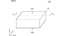
- FIG. 1 is an external perspective view of the resin multilayer substrate 101 according to the first embodiment.
- FIG. 2 is an exploded plan view of the resin multilayer substrate 101.
- FIG. 3 is a cross-sectional view taken along the line AA in FIG. 4-1 and 4-2 and 4-3 are cross-sectional views showing the manufacturing method of the resin multilayer substrate 101 in order.
- FIG. 5 is an external perspective view of the resin multilayer substrate 102 according to the second embodiment.
- FIG. 6 is an exploded plan view of the resin multilayer substrate 102.
- FIG. 7 is a cross-sectional view taken along the line BB in FIG.
- FIG. 1 is an external perspective view of the resin multilayer substrate 101 according to the first embodiment.
- FIG. 2 is an exploded plan view of the resin multilayer substrate 101.
- FIG. 3 is a cross-sectional view taken along the line AA in FIG. In FIG. 2, in order to make the structure easy to understand, the first openings AP11 and AP12 and the second openings AP21 and AP22 are shown in a dot pattern.
- the resin multilayer substrate 101 includes a laminate 10, a coil L1, external electrodes P1, P2, and the like.
- the coil L1 is configured to include a plurality of coil conductor patterns (first coil conductor patterns CP11, CP12 and second coil conductor patterns CP21, CP22), and has a winding shaft AX in the Z-axis direction. Have.
- the laminated body 10 is a rectangular parallelepiped whose longitudinal direction coincides with the X-axis direction. Further, the laminated body 10 has a first main surface VS1 and a second main surface VS2 facing each other.
- the coil L1 is formed inside the laminated body 10.
- the external electrodes P1 and P2 are exposed on the second main surface VS2 of the laminated body 10 (provided on the second main surface VS2 side).
- the laminated body 10 is formed by laminating the resin layers 16, 15, 14, 13, 12, and 11 in this order and thermocompression bonding.
- the first main surface VS1 and the second main surface VS2 of the laminated body 10 are planes orthogonal to the laminating direction (Z-axis direction) of the plurality of resin layers 11, 12, 13, 14, 15, and 16.
- the resin layers 11 to 16 are all rectangular flat plates whose longitudinal directions coincide with the X-axis direction. Each of the resin layers 11 to 16 has flexibility.
- the resin layers 11 to 16 are sheets containing, for example, a liquid crystal polymer (LCP) or a polyetheretherketone (PEEK) as a main component.
- LCP liquid crystal polymer
- PEEK polyetheretherketone
- the first coil conductor pattern CP11 is formed on the back surface of the resin layer 11.
- the first coil conductor pattern CP11 is a rectangular loop-shaped conductor pattern having about one turn wound around the outer circumference of the resin layer 11.
- the first coil conductor pattern CP11 is a conductor pattern such as Cu foil.
- a second coil conductor pattern CP21 and a conductor pattern 23 are formed on the back surface of the resin layer 12.
- the second coil conductor pattern CP21 is a rectangular loop-shaped conductor pattern of about one turn formed along the outer circumference of the resin layer 12.
- the conductor pattern 23 is a rectangular conductor pattern arranged near the first corner of the resin layer 12 (lower left corner of the resin layer 12 in FIG. 2).
- the second coil conductor pattern CP21 and the conductor pattern 23 are conductor patterns such as Cu foil. Further, interlayer connection conductors V4 and V5 are formed on the resin layer 12.
- the first opening AP11 is formed on the surface of the resin layer 12.
- the first opening AP11 is a rectangular loop-shaped recess (groove), and has a planar shape along the outer circumference of the second coil conductor pattern CP21 when viewed from the Z-axis direction.
- the first coil conductor pattern CP12 and the conductor pattern 22 are formed on the back surface of the resin layer 13.
- the first coil conductor pattern CP12 is a rectangular loop-shaped conductor pattern of about one turn formed along the outer circumference of the resin layer 13.
- the conductor pattern 22 is a rectangular conductor pattern arranged near the first corner of the resin layer 13 (lower left corner of the resin layer 13 in FIG. 2).
- the first coil conductor pattern CP12 and the conductor pattern 22 are conductor patterns such as Cu foil. Further, interlayer connection conductors V3 and V6 are formed on the resin layer 13.
- the second opening AP21 is formed on the surface of the resin layer 13.
- the second opening AP21 is a rectangular loop-shaped recess (groove), and has a planar shape along the inner circumference of the first coil conductor pattern CP12 when viewed from the Z-axis direction.
- a second coil conductor pattern CP22 and a conductor pattern 21 are formed on the back surface of the resin layer 14.
- the second coil conductor pattern CP22 is a rectangular loop-shaped conductor pattern of about one turn formed along the outer circumference of the resin layer 14.
- the conductor pattern 21 is a rectangular conductor pattern arranged near the first corner of the resin layer 14 (lower left corner of the resin layer 14 in FIG. 2).
- the second coil conductor pattern CP22 and the conductor pattern 21 are conductor patterns such as Cu foil. Further, interlayer connection conductors V2 and V7 are formed on the resin layer 14.
- the first opening AP12 is formed on the surface of the resin layer 14.
- the first opening AP11 is a rectangular loop-shaped recess (groove), and has a planar shape along the outer circumference of the second coil conductor pattern CP22 when viewed from the Z-axis direction.
- External electrodes P1 and P2 are formed on the back surface of the resin layer 15.
- the external electrodes P1 and P2 are rectangular conductor patterns whose longitudinal directions coincide with the Y-axis direction.
- the external electrode P1 is arranged near the first side of the resin layer 15 (the left side of the resin layer 15 in FIG. 2).
- the external electrode P2 is arranged near the second side of the resin layer 15 (the right side of the resin layer 15 in FIG. 2).
- the external electrodes P1 and P2 are conductor patterns such as Cu foil. Further, interlayer connection conductors V1 and V8 are formed on the resin layer 15.
- a second opening AP22 is formed on the surface of the resin layer 15.
- the second opening AP22 is a concave portion (groove) having a substantially ring-shaped planar shape.
- the second opening AP22 is arranged between the external electrodes P1 and P2 when viewed from the Z-axis direction.
- the openings HP1 and HP2 are formed in the resin layer 16.
- the opening HP1 is a rectangular through hole arranged near the first side of the resin layer 16 (the left side of the resin layer 16 in FIG. 2).
- the opening HP2 is a rectangular through hole arranged near the second side of the resin layer 16 (the right side of the resin layer 16 in FIG. 2).
- the opening HP1 is provided at a position corresponding to the position of the external electrode P1.
- the opening HP2 is provided at a position corresponding to the position of the external electrode P2. Therefore, even when the resin layer 16 is laminated on the back surface of the resin layer 15, the external electrode P1 is exposed to the outside from the opening HP1 and the external electrode P2 is exposed to the outside from the opening HP2.
- one end of the first coil conductor pattern CP11 is connected to one end of the second coil conductor pattern CP21 via the interlayer connection conductor V5. Further, the other end of the second coil conductor pattern CP21 is connected to one end of the first coil conductor pattern CP12 via the interlayer connection conductor V6. Further, the other end of the first coil conductor pattern CP12 is connected to one end of the second coil conductor pattern CP22 via the interlayer connection conductor V7.
- two or more coil conductor patterns (first coil conductor patterns CP11, CP12 and second coil conductor patterns CP21, CP22) and interlayer connection conductors V5, V6 formed on the two or more resin layers 11 to 14, respectively. , V7 constitute a coil L1 having a winding shaft AX in the Z-axis direction.
- the first end of the coil L1 is connected to the external electrode P1, and the second end of the coil L1 is connected to the external electrode P2.
- the other end of the first coil conductor pattern CP11 is connected to the external electrode P1 via the conductor patterns 21, 22, 23 and the interlayer connection conductors V1, V2, V3, V4.
- the other end of the second coil conductor pattern CP22 is connected to the external electrode P2 via the interlayer connection conductor V8.
- the first coil conductor patterns CP11 and CP12 and the second coil conductor patterns CP21 and CP22 are alternately arranged in the Z-axis direction.
- the first coil conductor patterns CP11 and CP12 and the second coil conductor patterns CP21 and CP22 are the first coil conductor pattern CP11, the second coil conductor pattern CP21, the first coil conductor pattern CP12 and the second coil conductor pattern. They are arranged in the ⁇ Z direction in the order of CP22.
- the first coil conductor pattern CP11 has a first overlapping portion OP11 that overlaps the second coil conductor pattern CP21 adjacent to the Z-axis direction when viewed from the Z-axis direction, and a first non-overlapping portion that does not overlap the second coil conductor pattern CP21. It has NOP11 and.
- the first non-overlapping portion NOP 11 has a radial direction (a direction parallel to the XY axis direction and a radial direction centered on the winding axis AX) with respect to the second coil conductor pattern CP21 adjacent to the Z axis direction. For example, FIG. It protrudes toward the outer peripheral side in the X-axis direction in 3. Further, in the Z-axis direction, the first non-overlapping portion NOP11 is curved so as to be closer to the second coil conductor pattern CP21 than the first overlapping portion OP11.
- the first coil conductor pattern CP12 has a first overlapping portion OP12 that overlaps the second coil conductor patterns CP21 and CP22 that are adjacent in the Z-axis direction when viewed from the Z-axis direction, and a second coil conductor pattern CP21 that does not overlap the second coil conductor patterns CP21 and CP22. It has 1 non-overlapping portion NOP12 and.
- the first non-overlapping portion NOP 12 protrudes to the outer peripheral side in the radial direction from the second coil conductor patterns CP21 and CP22 adjacent in the Z-axis direction. Further, in the Z-axis direction, the first non-overlapping portion NOP12 is curved so as to be closer to the second coil conductor pattern CP22 than the first overlapping portion OP12.
- the second coil conductor pattern CP21 has a second overlapping portion OP21 that overlaps the first coil conductor patterns CP11 and CP12 that are adjacent in the Z-axis direction when viewed from the Z-axis direction, and a second coil conductor pattern CP11 that does not overlap the first coil conductor patterns CP11 and CP12. It has two non-overlapping portions NOP21.
- the second non-overlapping portion NOP 21 projects to the inner peripheral side in the radial direction from the first coil conductor patterns CP11 and CP12 adjacent to each other in the Z-axis direction. Further, in the Z-axis direction, the second non-overlapping portion NOP21 is curved so as to be closer to the first coil conductor pattern CP12 than the second overlapping portion OP21.
- the second coil conductor pattern CP22 has a second overlapping portion OP22 that overlaps the first coil conductor pattern CP12 adjacent in the Z-axis direction and a second non-overlapping portion that does not overlap the first coil conductor pattern CP12 when viewed from the Z-axis direction. It has NOP22 and.
- the second non-overlapping portion NOP 22 projects to the inner peripheral side in the radial direction from the first coil conductor pattern CP12 adjacent in the Z-axis direction.
- the second coil conductor pattern CP22 of the present embodiment is located closest to the external electrodes P1 and P2 in the Z-axis direction among the plurality of coil conductor patterns (external electrodes in the Z-axis direction). It is located closest to P1 and P2).
- the second overlapping portion OP22 corresponds to an “electrode overlapping portion” that also overlaps with the external electrodes P1 and P2 when viewed from the Z-axis direction.
- the second non-overlapping portion NOP22 corresponds to an "electrode non-overlapping portion” that does not overlap the external electrodes P1 and P2 when viewed from the Z-axis direction.
- the second non-overlapping portion NOP22 (electrode non-overlapping portion) is curved so as to be closer to the external electrodes P1 and P2 than the second overlapping portion OP22 (electrode overlapping portion) in the Z-axis direction.
- the coil conductor pattern having a narrow wire width is more likely to be displaced due to the flow of the resin during thermocompression bonding (when forming a laminate) than the coil conductor pattern having a wide wire width. Therefore, for the purpose of suppressing misalignment of the coil conductor pattern during thermocompression bonding, a resin multilayer substrate having a coil conductor pattern provided with a wider portion having a wider line width than other coil conductor patterns can be considered. As a result, misalignment of the wide portion during thermocompression bonding is suppressed. However, even with this configuration, due to the flow of the resin during thermocompression bonding, some misalignment or the like occurs in the narrow portion whose line width is narrower than that of the wide portion.
- the coil conductor patterns having a large line width may overlap each other when viewed from the stacking direction. At this time, the unnecessary capacitance generated in the portion where the coil conductor patterns having a large line width overlap each other becomes very large.
- the non-overlapping portions of the two coil conductor patterns (first coil conductor pattern and second coil conductor pattern) adjacent to each other in the stacking direction (Z-axis direction) are formed. They project in opposite directions in the radial direction. Therefore, the coil conductor patterns adjacent to each other in the Z-axis direction are alternately arranged on the inner peripheral side and the outer peripheral side in the radial direction.
- the non-overlapping portions of the first coil conductor pattern and the second coil conductor pattern adjacent to each other in the Z-axis direction (for example, the first non-overlapping portion NOP11 and the second non-overlapping portion NOP21, the first non-overlapping portion)
- the NOP12 and the second non-overlapping portions NOP21, NOP22) do not overlap when viewed from the Z-axis direction. Therefore, according to this configuration, even when the line width of the coil conductor patterns adjacent to each other in the stacking direction is thick, it is possible to reduce the portions that overlap each other when viewed from the stacking direction. Therefore, unnecessary capacitance formation between (non-overlapping portions) of two adjacent coil conductor patterns is suppressed.
- the first non-overlapping portion NOP11 of the first coil conductor pattern CP11 and the second coil conductor pattern CP21 adjacent in the Z-axis direction are curved so as to be close to each other.
- the first non-overlapping portion NOP12 of the first coil conductor pattern CP12 and the second coil conductor pattern CP22 adjacent to each other in the Z-axis direction are curved so as to be close to each other in the stacking direction.
- the curved first non-overlapping portions NOP11 and NOP12 suppress the flow of the resin near the second coil conductor patterns CP21 and CP22 during thermocompression bonding. Therefore, the misalignment of the second coil conductor patterns CP21 and CP22 due to the flow of the resin during thermocompression bonding is suppressed.
- the second non-overlapping portion NOP21 of the second coil conductor pattern CP21 and the first coil conductor pattern CP12 adjacent in the Z-axis direction are curved so as to be close to each other. .. Therefore, as a result, the misalignment of the first coil conductor pattern CP12 during thermocompression bonding is suppressed.
- the second non-overlapping portion NOP22 (electrode non-overlapping portion) of the second coil conductor pattern CP22 located closest to the external electrodes P1 and P2 in the Z-axis direction is located in the Z-axis direction. , It is curved so as to be closer to the external electrodes P1 and P2 than the second overlapping portion OP22 (electrode overlapping portion). As described above, the external electrodes P1 and P2 arranged on the second main surface VS2 side are likely to be displaced due to the flow of the resin during thermocompression bonding.
- the second non-overlapping portion NOP22 is curved so as to be close to the external electrodes P1 and P2 (second main surface VS2) in the Z-axis direction.
- the flow of the resin near the external electrodes P1 and P2 which tends to flow during thermocompression bonding, is suppressed. Therefore, the displacement of the external electrodes P1 and P2 is suppressed.
- the non-overlapping portions NOP12 and NOP21 are also provided in the coil conductor patterns on the inner layer side other than the first main surface side coil conductor pattern and the second main surface side coil conductor pattern. Has been done. According to this configuration, the non-overlapping portions provided in the first main surface side coil conductor pattern and the second main surface side coil conductor pattern suppress the flow of the resin during thermocompression bonding, and the other coils on the inner layer side. The non-overlapping portion provided in the conductor pattern suppresses the flow of the resin during thermocompression bonding.
- the first main surface side coil conductor pattern is, for example, the first coil conductor pattern CP11 located closest to the first main surface VS1 in the Z-axis direction among a plurality of coil conductor patterns. is there.
- the second main surface side coil conductor pattern is, for example, the second coil conductor pattern CP22 located closest to the second main surface VS2 in the Z-axis direction among a plurality of coil conductor patterns.
- the other coil conductor patterns located on the inner layer side are, for example, the first coil conductor pattern CP12 and the second coil conductor pattern CP21.
- the non-overlapping portion provided in one coil conductor pattern is Z. It is preferable that they are arranged on at least two opposite sides (for example, the left side and the right side of the first coil conductor pattern in FIG. 2) when viewed from the axial direction. According to this configuration, the non-overlapping portions provided on the two sides facing each other effectively suppress the misalignment of the coil (or coil conductor pattern) due to the flow of the resin during thermocompression bonding.
- the non-overlapping portion provided in a certain coil conductor pattern is , It is preferable that the coils are provided on three or more sides when viewed from the Z-axis direction. According to this configuration, the effect of suppressing the misalignment of the coil due to the non-overlapping portion is further enhanced as compared with the case where the non-overlapping portion is provided on the two sides when viewed from the Z-axis direction.
- the resin multilayer substrate of the present invention is not limited to this configuration.
- the inner and outer shapes of the coil conductor pattern can be changed as appropriate.
- the inner and outer shapes of the coil conductor pattern may be circular, elliptical, L-shaped, or the like.
- the non-overlapping portion provided in a certain coil conductor pattern is in four directions (for example, + X direction, + Y direction, and ⁇ X direction) orthogonal to the winding axis AX of the coil when viewed from the Z axis direction. And ⁇ Y direction), it is preferable that they are located in at least two directions.
- the non-overlapping portion is located in two parallel directions (for example, + X direction and ⁇ X direction) among the four orthogonal directions viewed from the Z axis direction with respect to the winding axis AX, respectively.
- the displacement of the coil due to the flow of the resin during thermocompression bonding is effectively suppressed.
- the non-overlapping portion is arranged so as to surround the winding axis AX when viewed from the Z-axis direction (from the Z-axis direction). It is preferably located in at least three of the four orthogonal directions viewed). As a result, the effect of suppressing the misalignment of the coil due to the non-overlapping portion is further enhanced.
- the resin multilayer substrate 101 in which the non-overlapping portion is provided over the entire length of one coil conductor pattern is shown.
- the resin multilayer substrate of the present invention is not limited to this configuration. If the non-overlapping portion provided in a certain coil conductor pattern is provided in a portion of 1/5 or more of the total length of the coil conductor pattern, the action / effect of the present invention can be obtained. Further, the number of turns of the first coil conductor pattern and the second coil conductor pattern is not limited to one turn, respectively. It may be different for each coil conductor pattern.
- the resin multilayer substrate 101 according to this embodiment is manufactured by, for example, the following manufacturing method.
- 4-1 and 4-2 and 4-3 are cross-sectional views showing the manufacturing method of the resin multilayer substrate 101 in order.
- FIGS. 4-1 and 4-2 and 4-3 for convenience of explanation, the one-chip (individual piece) manufacturing process will be described, but the actual manufacturing process of the resin multilayer substrate 101 is in the assembled substrate state. Will be done.
- the “aggregate substrate” refers to a substrate including a plurality of resin multilayer substrates 101. This also applies to each cross-sectional view showing the subsequent manufacturing process of the resin multilayer substrate.
- the resin layers 11 to 16 are sheets such as, for example, a liquid crystal polymer (LCP) or a polyetheretherketone (PEEK).
- LCP liquid crystal polymer
- PEEK polyetheretherketone
- first coil conductor patterns CP11, CP12 and second coil conductor patterns CP21, CP22 are formed on the resin layers 11 to 15.
- a metal foil for example, Cu foil
- the metal leaf is patterned by photolithography.
- the first coil conductor pattern CP11 is formed on the back surface of the resin layer 11
- the second coil conductor pattern CP21 is formed on the back surface of the resin layer 12
- the first coil conductor pattern CP12 is formed on the back surface of the resin layer 13.
- a second coil conductor pattern CP22 is formed on the back surface of the resin layer 14.
- the external electrodes P1 and P2 are formed on the back surface of the resin layer 15.
- the step of forming a plurality of coil conductor patterns (first coil conductor patterns CP11, CP12 and second coil conductor patterns CP21, CP22) on two or more resin layers 11 to 14, respectively, is the step of forming the "coil" of the present invention.
- This is an example of the "conductor forming process”.
- interlayer connecting conductors are formed on the resin layers 11 to 15.
- a conductive paste containing a metal powder such as Cu, Sn or an alloy thereof and a resin material is arranged (filled) in the holes. , It is provided by solidifying the conductive paste by subsequent thermal pressure bonding.
- openings HP1 and HP2 are formed in the resin layer 16.
- the opening HP1 is a rectangular through hole arranged in the vicinity of the first side of the resin layer 16 (the left side of the resin layer 16 in FIGS. 4-1, 4-2 and 4-3).
- the opening HP2 is a rectangular through hole arranged in the vicinity of the second side of the resin layer 16 (the right side of the resin layer 16 in FIGS. 4-1, 4-2 and 4-3).
- the openings HP1 and HP2 are formed by etching the resin layer 16 with, for example, a laser or the like. Further, the openings HP1 and HP2 may be formed by punching or the like.
- the first opening AP11 having a predetermined shape is formed on the resin layer 12, and the first opening AP12 having a predetermined shape is formed on the resin layer 14.
- the first opening AP11 is a recess (groove) having substantially the same shape as the first non-overlapping portion NOP11 of the first coil conductor pattern CP11.
- the first opening AP12 is a recess (groove) having substantially the same shape as the first non-overlapping portion NOP12 of the first coil conductor pattern CP12.
- the resin layer 13 is formed with the second opening AP21 having a predetermined shape
- the resin layer 15 is formed with the second opening AP22 having a predetermined shape.
- the second opening AP21 is a recess (groove) having substantially the same shape as the second coil conductor pattern CP21.
- the second opening AP21 is a recess (groove) having substantially the same shape as the second non-overlapping portion NOP21 of the second coil conductor pattern CP21.
- the second opening AP22 is a recess (groove) having substantially the same shape as the second non-overlapping portion NOP22 of the second coil conductor pattern CP22.
- the step of forming the first openings AP11, AP12 and the second openings AP21, AP22 having a predetermined shape in the plurality of resin layers 12 to 15, respectively, is an example of the "opening forming step" of the present invention.
- the first coil conductor patterns CP11 and CP12 and the second coil conductor patterns CP21 and CP22 are laminated (placed) so as to be alternately arranged in the Z-axis direction.
- the resin layers 11 to 16 are laminated (placed) in the order of the resin layers 16, 15, 14, 13, 12, and 11.
- the first coil conductor pattern CP11 has a first overlapping portion OP11 that overlaps the second coil conductor pattern CP21 adjacent to the Z-axis direction when viewed from the Z-axis direction, and a first overlapping portion OP11 that does not overlap the second coil conductor pattern.
- the non-overlapping portion NOP 11 is formed.
- the first coil conductor pattern CP12 has a first overlapping portion OP12 overlapping the second coil conductor patterns CP21 and CP22 adjacent to the Z-axis direction when viewed from the Z-axis direction, and the second coil conductor patterns CP21 and CP22.
- a first non-overlapping portion NOP12 that does not overlap is formed.
- the second coil conductor pattern CP21 has a second overlapping portion OP21 overlapping the first coil conductor patterns CP11 and CP12 adjacent to the Z-axis direction when viewed from the Z-axis direction, and the first coil conductor patterns CP11 and CP12.
- a second non-overlapping portion NOP21 that does not overlap is formed.
- the second coil conductor pattern CP22 has a second overlapping portion OP22 that overlaps the first coil conductor pattern CP12 adjacent to the Z-axis direction when viewed from the Z-axis direction, and a second overlapping portion OP22 that does not overlap the first coil conductor pattern CP12.
- the non-overlapping portion NOP 22 is formed.
- the first non-overlapping portion NOP11 of the first coil conductor pattern CP11 is on the outer peripheral side in the radial direction (for example, the X-axis direction in FIGS. 4-1, 4-2 and 4-3) with respect to the second coil conductor pattern CP21. Protruding into. Further, the first non-overlapping portion NOP12 of the first coil conductor pattern CP12 projects toward the outer peripheral side in the radial direction with respect to the second coil conductor patterns CP21 and CP22. Further, the second non-overlapping portion NOP21 of the second coil conductor pattern CP21 projects toward the inner peripheral side in the radial direction with respect to the first coil conductor patterns CP11 and CP12. The second non-overlapping portion NOP22 of the second coil conductor pattern CP22 projects toward the inner peripheral side in the radial direction with respect to the first coil conductor pattern CP12.
- the first opening AP11 overlaps the first non-overlapping portion NOP11 and the first opening AP12 overlaps the first non-overlapping portion NOP12 when viewed from the Z-axis direction. .. Further, when the plurality of resin layers 11 to 16 are laminated, the second opening AP21 overlaps the second non-overlapping portion NOP21 and the second opening AP22 overlaps the second non-overlapping portion NOP22 when viewed from the Z-axis direction. ..
- the resin layers 11 to 16 are arranged so that the first coil conductor patterns CP11 and CP12 and the second coil conductor patterns CP21 and CP22 are alternately arranged in the Z-axis direction after the “coil conductor forming step”. Is an example of the "lamination process" of the present invention.
- the plurality of laminated resin layers 11 to 16 are thermocompression bonded (collectively pressed) to form the laminated body 10 (resin multilayer substrate 101) shown in FIG. 4-3. Specifically, while heating the plurality of laminated resin layers 11 to 16, a pseudo isotropic pressure press (pressurization) is performed from the direction of the white arrow shown in FIG. 4-2.
- the first non-overlapping portions NOP11 and NOP12 of the first coil conductor patterns CP11 and CP12 have a smaller number of overlapping conductor patterns when viewed from the Z-axis direction than the first overlapping portions OP11 and OP12. Therefore, the resin near the first non-overlapping portions NOP11 and NOP12 at the time of thermocompression bonding is more easily deformed than the vicinity of the first overlapping portions OP11 and OP12. Therefore, the first non-overlapping portion NOP11 of the first coil conductor pattern CP11 is curved so as to be closer to the second coil conductor pattern CP21 than the first overlapping portion OP11 in the stacking direction. Further, the first non-overlapping portion NOP12 of the first coil conductor pattern CP12 is curved so as to be closer to the second coil conductor pattern CP22 than the first overlapping portion OP12 in the stacking direction.
- the second non-overlapping portions NOP21 and NOP22 of the second coil conductor patterns CP21 and CP22 have a smaller number of overlapping conductor patterns when viewed from the Z-axis direction than the second overlapping portions OP21 and OP22. Therefore, the resin near the second non-overlapping portions NOP21 and NOP22 at the time of thermocompression bonding is more easily deformed than the vicinity of the second overlapping portions OP21 and OP22. Therefore, the second non-overlapping portion NOP21 of the second coil conductor pattern CP21 is curved so as to be closer to the first coil conductor pattern CP12 than the second overlapping portion OP21 in the stacking direction. Further, the second non-overlapping portion NOP22 of the second coil conductor pattern CP22 is curved so as to be closer to the external electrodes P1 and P2 than the second overlapping portion OP22 in the stacking direction.
- the step of forming the laminated body 10 by thermocompression bonding the plurality of laminated resin layers 11 to 16 after the "laminated step” is an example of the “laminated body forming step” of the present invention.
- the first openings AP11 and AP12 are provided at positions overlapping the first non-overlapping portions NOP11 and NOP12, respectively, and the second opening is provided at a position overlapping the second non-overlapping portions NOP21 and NOP22.
- AP21 and AP22 are provided respectively.
- the opening provided at the position where the non-overlapping portion overlaps is a recess (groove). Therefore, as compared with the case where the opening is a through hole (detailed later), a short circuit due to the curvature of the non-overlapping portion during thermocompression bonding (particularly, a short circuit between coil conductor patterns adjacent in the Z-axis direction). Can be suppressed.
- the first opening AP11 is formed on the surface of the resin layer 12 (the resin layer in contact with the first non-overlapping part NOP11), and the surface of the resin layer 14 (the resin layer in contact with the first non-overlapping part NOP12).
- An example in which the first opening AP12 was formed was shown.
- the first opening AP11 may be formed on, for example, the back surface of the resin layer 12, or may be formed on both the front surface and the back surface of the resin layer 12.
- the first opening AP12 may be formed on the back surface of the resin layer 14, or may be formed on both the front surface and the back surface of the resin layer 14.
- the second opening AP21 may be formed on, for example, the back surface of the resin layer 13, or may be formed on both the front surface and the back surface of the resin layer 13. Further, the second opening AP22 may be formed on the back surface of the resin layer 15, or may be formed on both the front surface and the back surface of the resin layer 15.
- first openings AP11 and AP12 and the second openings AP21 and AP22 are not limited to the recesses (grooves).
- the first opening AP11, AP12 and the second opening AP21, AP22 may be through holes penetrating from the front surface to the back surface of the resin layer.
- the non-overlapping portions first non-overlapping portions NOP11, NOP12 and second non-overlapping portions NOP21, NOP22
- a short circuit is likely to occur between the first coil conductor pattern and the second coil conductor pattern.
- the opening when the opening is a through hole, it is preferable to form a laminated body by sandwiching another resin layer in which the opening is not formed between the non-overlapping portion and the opening. Specifically, it is preferable to sandwich different resin layers between the resin layers 11 and 12, between the resin layers 12 and 13, and between the resin layers 13 and 14, respectively.
- the second embodiment shows an example of a resin multilayer substrate having a plurality of spiral coil conductor patterns.
- FIG. 5 is an external perspective view of the resin multilayer substrate 102 according to the second embodiment.
- FIG. 6 is an exploded plan view of the resin multilayer substrate 102.
- FIG. 7 is a cross-sectional view taken along the line BB in FIG.
- the wide portions WP11 and WP12 of the first coil conductor patterns CP11A and CP12A and the wide portions WP21 and WP22 of the second coil conductor patterns CP21A and CP22A are shown by hatching in order to make the structure easy to understand.
- the resin multilayer substrate 102 includes a laminate 10A, a coil L2, external electrodes P1A, P2A, and the like.
- the length of the laminated body 10A in the longitudinal direction (X-axis direction) is longer than that of the laminated body 10 described in the first embodiment.
- Other configurations of the laminated body 10A are the same as those of the laminated body 10.
- the laminated body 10A is formed by laminating the resin layers 16a, 15a, 14a, 13a, 12a, and 11a in this order and thermocompression bonding.
- the length of the resin layers 11a to 16a in the longitudinal direction is longer than that of the resin layers 11 to 16 described in the first embodiment.
- Other configurations of the resin layers 11a to 16a are the same as those of the resin layers 11 to 16.
- the first coil conductor pattern CP11A is formed on the back surface of the resin layer 11a.
- the first coil conductor pattern CP11A is arranged near the center of the resin layer 11a in the longitudinal direction.
- the first coil conductor pattern CP11A is a rectangular spiral conductor pattern having about 2.75 turns.
- the first coil conductor pattern CP11A has a wide portion WP11 at the outermost peripheral portion in the radial direction (about one winding portion located on the outermost peripheral side).
- a second coil conductor pattern CP21A and a conductor pattern 23 are formed on the back surface of the resin layer 12a.
- the second coil conductor pattern CP21A is arranged near the center of the resin layer 12a in the longitudinal direction.
- the second coil conductor pattern CP21A is a rectangular spiral conductor pattern having about 3 turns.
- the second coil conductor pattern CP21A has a wide portion WP21 at the innermost peripheral portion in the radial direction (about one winding portion located on the innermost peripheral side).
- the conductor pattern 23 is the same as that described in the first embodiment.
- the first coil conductor pattern CP12A and the conductor pattern 22 are formed on the back surface of the resin layer 13a.
- the first coil conductor pattern CP12A is arranged near the center of the resin layer 13a in the longitudinal direction.
- the first coil conductor pattern CP12A is a rectangular spiral conductor pattern having about 3 turns.
- the first coil conductor pattern CP12A has a wide portion WP12 at the outermost peripheral portion in the radial direction.
- the conductor pattern 22 is the same as that described in the first embodiment.
- a second coil conductor pattern CP22A and a conductor pattern 21 are formed on the back surface of the resin layer 14a.
- the second coil conductor pattern CP22A is arranged near the center of the resin layer 14 in the longitudinal direction.
- the second coil conductor pattern CP22A is a rectangular spiral conductor pattern having about 3 turns.
- the second coil conductor pattern CP22A has a wide portion WP22 at the innermost peripheral portion in the radial direction.
- the conductor pattern 21 is the same as that described in the first embodiment.
- External electrodes P1A and P2A are formed on the back surface of the resin layer 15a.
- the external electrode P1A is the same as the external electrode P1 described in the first embodiment.
- the external electrode P2A is arranged near the second side of the resin layer 15a (the right side of the resin layer 15a in FIG. 6).
- the external electrode P2A is an L-shaped conductor pattern.
- openings HP1 and HP2 are formed in the resin layer 16a. The openings HP1 and HP2 are the same as those described in the first embodiment.
- one end of the first coil conductor pattern CP11A is connected to one end of the second coil conductor pattern CP21A via the interlayer connection conductor V5. Further, the other end of the second coil conductor pattern CP21A is connected to one end of the first coil conductor pattern CP12A via the interlayer connection conductor V6. The other end of the first coil conductor pattern CP12A is connected to one end of the second coil conductor pattern CP22A via the interlayer connection conductor V7.
- the three or more coil conductor patterns (first coil conductor patterns CP11A, CP12A and the second coil conductor patterns CP21A, CP22A) and the interlayer connection conductors V5, V6, respectively, which are formed in the three or more resin layers 11a to 14a, respectively.
- the V7 constitutes a coil L2 having a winding shaft AX in the Z-axis direction.
- first end of the coil L2 is connected to the external electrode P1A.
- second end of the coil L2 is connected to the external electrode P2A.
- the other end of the first coil conductor pattern CP11A is connected to the external electrode P1A via the conductor patterns 21, 22, 23 and the interlayer connection conductors V1, V2, V3, V4.
- the other end of the second coil conductor pattern CP22A is connected to the external electrode P2A via the interlayer connection conductor V8.
- the first coil conductor patterns CP11A and CP12A and the second coil conductor patterns CP21A and CP22A are alternately arranged in the Z-axis direction.
- the first coil conductor patterns CP11A, CP12A and the second coil conductor patterns CP21A, CP22A are the first coil conductor pattern CP11A, the second coil conductor pattern CP21A, the first coil conductor pattern CP12A, and the second coil conductor pattern. They are arranged in the ⁇ Z direction in the order of CP22A.
- the wide portion (outermost peripheral portion) of the first coil conductor pattern CP11A includes a first overlapping portion OP11 that overlaps the second coil conductor pattern CP21 adjacent to the Z axis when viewed from the Z axis direction. It has a first non-overlapping portion NOP11 that does not overlap with the second coil conductor pattern CP21A.
- the first non-overlapping portion NOP 11 projects to the outer peripheral side in the radial direction from the second coil conductor pattern CP21. Further, the first non-overlapping portion NOP11 is curved so as to be closer to the second coil conductor pattern CP21A than the first overlapping portion OP11.
- the wide portion (innermost peripheral portion) of the second coil conductor pattern CP21A includes a second overlapping portion OP21 overlapping the first coil conductor patterns CP11A and CP12A adjacent to each other in the Z-axis direction and a first coil. It has a second non-overlapping portion NOP21 that does not overlap with the conductor patterns CP11A and CP12A.
- the second non-overlapping portion NOP21 projects to the inner peripheral side in the radial direction from the first coil conductor patterns CP11A and CP12A. Further, the second non-overlapping portion NOP21 is curved so as to be closer to the first coil conductor pattern CP12A than the second overlapping portion NOP21.
- the wide portion (outermost peripheral portion) of the first coil conductor pattern CP12A includes a first overlapping portion OP12 overlapping the second coil conductor patterns CP21A and CP22A adjacent to each other in the Z-axis direction and a second coil conductor. It has a first non-overlapping portion NOP12 that does not overlap with the patterns CP21A and CP22A.
- the first non-overlapping portion NOP12 projects to the outer peripheral side in the radial direction from the second coil conductor patterns CP21A and CP22A. Further, the first non-overlapping portion NOP12 is curved so as to be closer to the second coil conductor pattern CP22A than the first overlapping portion OP12.
- the wide portion (innermost peripheral portion) of the second coil conductor pattern CP22A includes a second overlapping portion OP22 that overlaps the first coil conductor pattern CP12A adjacent to the Z-axis direction when viewed from the Z-axis direction, and a first coil conductor pattern. It has a second non-overlapping portion NOP22 that does not overlap the CP12A.
- the second non-overlapping portion NOP 22 projects to the inner peripheral side in the radial direction from the first coil conductor pattern CP12A. Further, the second non-overlapping portion NOP22 is curved so as to be closer to the second main surface VS2 than the second overlapping portion OP22.
- the plurality of coil conductor patterns may each have a spiral shape of two or more turns.
- the plurality of coil conductor patterns are not limited to the configuration in which the number of turns is substantially the same. That is, the plurality of coil conductor patterns may have different turns.
- the wide portions WP11 and WP12 are located only on the outermost peripheral portions in the radial direction of the spiral first coil conductor patterns CP11A and CP12A, but the configuration is not limited to this. Absent.
- the wide portions WP11 and WP12 may be formed in a portion other than the outermost peripheral portion of the spiral first coil conductor pattern, or the entire first coil conductor pattern may be a wide portion.
- the wide portions WP21 and WP22 may be formed in a portion other than the innermost peripheral portion of the spiral second coil conductor patterns CP21A and CP22A, and the entire second coil conductor pattern may be a wide portion. Good.
- the laminated body is a rectangular parallelepiped having a longitudinal direction in the X-axis direction, but the shape of the laminated body is not limited to this.
- the shape of the laminate can be appropriately changed within the range in which the action and effect of the present invention are exhibited.
- the planar shape of the laminated body may be, for example, polygonal, circular, elliptical, L-shaped, U-shaped, crank-shaped, T-shaped, Y-shaped, or the like.
- thermocompression bonding six resin layers an example of a laminated body formed by thermocompression bonding six resin layers is shown.
- the laminate of the present invention is not limited to this.
- the number of layers of the resin layer forming the laminate can be changed as appropriate.
- a protective film such as a coverlay film or a resist film may be formed on the surface of the laminate.
- coils L1 and L2 in which the winding shaft AX coincides with the Z-axis direction are shown.
- the winding shaft AX of the coil is not limited to the one that exactly coincides with the Z-axis direction.
- "having a winding axis along the stacking direction of a plurality of resin layers” means, for example, a case where the winding axis AX of the coil is in the range of -30 ° to + 30 ° with respect to the Z-axis direction. Including.
- the first coil conductor pattern is located closest to the first main surface VS1 among the plurality of coil conductor patterns
- the second coil conductor pattern is the plurality of coil conductor patterns.
- An example of being located closest to the second main surface VS2 is shown.
- the arrangement of the first coil conductor pattern and the second coil conductor pattern is not limited to this configuration.
- the first coil conductor pattern and the second coil conductor pattern may be arranged alternately in the stacking direction.
- the second coil conductor pattern may be located closest to the first main surface VS1
- the first coil conductor pattern may be located closest to the second main surface VS2.
- the circuit configuration formed on the resin multilayer substrate is not limited to the configuration of each of the above-described embodiments, and can be appropriately changed as long as the operation and effect of the present invention are exhibited.
- the circuit formed on the resin multilayer substrate may be formed with, for example, a capacitor formed by a conductor pattern or a frequency filter such as various filters (low-pass filter, high-pass filter, band-pass filter, band-elimination filter).
- various transmission lines strip line, microstrip line, coplanar line, etc.
- various electronic components such as chip components may be mounted or embedded in the resin multilayer substrate.
- the planar shape, position, and number of the first coil conductor pattern, the second coil conductor pattern, and the external electrodes are not limited to the configurations of the above-described embodiments, and the actions and effects of the present invention are exhibited. It can be changed as appropriate within the range.
- the planar shape of the external electrode may be, for example, polygonal, circular, elliptical, arcuate, ring-shaped, L-shaped, U-shaped, T-shaped, Y-shaped, crank-shaped, or the like.
- the external electrodes may be formed only on the second main surface VS2, and the first main surface VS1 side (or on the first main surface VS1) and the second main surface VS2 side (or the second main surface). It may be formed on both surfaces (on surface VS2).
- the resin multilayer substrate may include a dummy electrode that is not connected to the circuit.
Landscapes
- Engineering & Computer Science (AREA)
- Power Engineering (AREA)
- Manufacturing & Machinery (AREA)
- Microelectronics & Electronic Packaging (AREA)
- Coils Or Transformers For Communication (AREA)
- Manufacturing Cores, Coils, And Magnets (AREA)
- Parts Printed On Printed Circuit Boards (AREA)
Priority Applications (3)
| Application Number | Priority Date | Filing Date | Title |
|---|---|---|---|
| JP2021533990A JP7127744B2 (ja) | 2019-07-19 | 2020-07-16 | 樹脂多層基板および樹脂多層基板の製造方法 |
| CN202090000725.XU CN216752238U (zh) | 2019-07-19 | 2020-07-16 | 树脂多层基板 |
| US17/569,548 US12586707B2 (en) | 2019-07-19 | 2022-01-06 | Multilayer resin substrate and method of manufacturing multilayer resin substrate |
Applications Claiming Priority (2)
| Application Number | Priority Date | Filing Date | Title |
|---|---|---|---|
| JP2019133246 | 2019-07-19 | ||
| JP2019-133246 | 2019-07-19 |
Related Child Applications (1)
| Application Number | Title | Priority Date | Filing Date |
|---|---|---|---|
| US17/569,548 Continuation US12586707B2 (en) | 2019-07-19 | 2022-01-06 | Multilayer resin substrate and method of manufacturing multilayer resin substrate |
Publications (1)
| Publication Number | Publication Date |
|---|---|
| WO2021015097A1 true WO2021015097A1 (ja) | 2021-01-28 |
Family
ID=74193074
Family Applications (1)
| Application Number | Title | Priority Date | Filing Date |
|---|---|---|---|
| PCT/JP2020/027689 Ceased WO2021015097A1 (ja) | 2019-07-19 | 2020-07-16 | 樹脂多層基板および樹脂多層基板の製造方法 |
Country Status (4)
| Country | Link |
|---|---|
| US (1) | US12586707B2 (https=) |
| JP (1) | JP7127744B2 (https=) |
| CN (1) | CN216752238U (https=) |
| WO (1) | WO2021015097A1 (https=) |
Cited By (1)
| Publication number | Priority date | Publication date | Assignee | Title |
|---|---|---|---|---|
| CN114974801A (zh) * | 2021-02-18 | 2022-08-30 | Tdk株式会社 | 层叠线圈部件 |
Families Citing this family (1)
| Publication number | Priority date | Publication date | Assignee | Title |
|---|---|---|---|---|
| JP7287216B2 (ja) * | 2019-09-24 | 2023-06-06 | Tdk株式会社 | コイル構造体 |
Citations (6)
| Publication number | Priority date | Publication date | Assignee | Title |
|---|---|---|---|---|
| JPH02110907A (ja) * | 1988-10-19 | 1990-04-24 | Toko Inc | 積層インダクタとそのインダクタンス調整方法 |
| JP2008118059A (ja) * | 2006-11-07 | 2008-05-22 | Tdk Corp | コモンモードチョークコイル |
| WO2015005161A1 (ja) * | 2013-07-11 | 2015-01-15 | 株式会社村田製作所 | 電子部品 |
| JP2015050422A (ja) * | 2013-09-04 | 2015-03-16 | 株式会社村田製作所 | 樹脂多層基板およびその製造方法 |
| WO2015079941A1 (ja) * | 2013-11-28 | 2015-06-04 | 株式会社村田製作所 | 多層基板の製造方法、多層基板および電磁石 |
| WO2018174133A1 (ja) * | 2017-03-24 | 2018-09-27 | 株式会社村田製作所 | 多層基板、アクチュエータおよび多層基板の製造方法 |
Family Cites Families (7)
| Publication number | Priority date | Publication date | Assignee | Title |
|---|---|---|---|---|
| JP3821083B2 (ja) * | 2002-10-11 | 2006-09-13 | 株式会社デンソー | 電子機器 |
| WO2009081865A1 (ja) * | 2007-12-26 | 2009-07-02 | Murata Manufacturing Co., Ltd. | 積層型電子部品及びこれを備えた電子部品モジュール |
| JP5636842B2 (ja) * | 2010-09-24 | 2014-12-10 | 株式会社村田製作所 | 多層アンテナの製造方法 |
| US8836460B2 (en) * | 2012-10-18 | 2014-09-16 | International Business Machines Corporation | Folded conical inductor |
| WO2015083525A1 (ja) * | 2013-12-06 | 2015-06-11 | 株式会社村田製作所 | インダクタ素子及び電子機器 |
| DE102015222400A1 (de) * | 2015-11-13 | 2017-06-08 | Schaeffler Technologies AG & Co. KG | Multilayer-Platine und Verfahren zu deren Herstellung |
| CN208273381U (zh) * | 2016-03-15 | 2018-12-21 | 株式会社村田制作所 | 电路基板 |
-
2020
- 2020-07-16 CN CN202090000725.XU patent/CN216752238U/zh active Active
- 2020-07-16 JP JP2021533990A patent/JP7127744B2/ja active Active
- 2020-07-16 WO PCT/JP2020/027689 patent/WO2021015097A1/ja not_active Ceased
-
2022
- 2022-01-06 US US17/569,548 patent/US12586707B2/en active Active
Patent Citations (6)
| Publication number | Priority date | Publication date | Assignee | Title |
|---|---|---|---|---|
| JPH02110907A (ja) * | 1988-10-19 | 1990-04-24 | Toko Inc | 積層インダクタとそのインダクタンス調整方法 |
| JP2008118059A (ja) * | 2006-11-07 | 2008-05-22 | Tdk Corp | コモンモードチョークコイル |
| WO2015005161A1 (ja) * | 2013-07-11 | 2015-01-15 | 株式会社村田製作所 | 電子部品 |
| JP2015050422A (ja) * | 2013-09-04 | 2015-03-16 | 株式会社村田製作所 | 樹脂多層基板およびその製造方法 |
| WO2015079941A1 (ja) * | 2013-11-28 | 2015-06-04 | 株式会社村田製作所 | 多層基板の製造方法、多層基板および電磁石 |
| WO2018174133A1 (ja) * | 2017-03-24 | 2018-09-27 | 株式会社村田製作所 | 多層基板、アクチュエータおよび多層基板の製造方法 |
Cited By (1)
| Publication number | Priority date | Publication date | Assignee | Title |
|---|---|---|---|---|
| CN114974801A (zh) * | 2021-02-18 | 2022-08-30 | Tdk株式会社 | 层叠线圈部件 |
Also Published As
| Publication number | Publication date |
|---|---|
| JP7127744B2 (ja) | 2022-08-30 |
| US20220130592A1 (en) | 2022-04-28 |
| US12586707B2 (en) | 2026-03-24 |
| CN216752238U (zh) | 2022-06-14 |
| JPWO2021015097A1 (https=) | 2021-01-28 |
Similar Documents
| Publication | Publication Date | Title |
|---|---|---|
| CN207250269U (zh) | 线圈内置多层基板 | |
| US8169288B2 (en) | Electronic component and method for making the same | |
| CN206976139U (zh) | 共模噪声滤波器 | |
| JP2014038884A (ja) | 電子部品および電子部品の製造方法 | |
| US11189413B2 (en) | Multilayer coil component and method for producing the same | |
| JP2013077849A (ja) | 電子部品 | |
| JP2002252117A (ja) | 積層型コイル部品及びその製造方法 | |
| JP2009278009A (ja) | コモンモードフィルタ | |
| KR20140021711A (ko) | 전자 부품 및 그 제조 방법 | |
| CN213124016U (zh) | 树脂多层基板以及致动器 | |
| WO2013108862A1 (ja) | コイル部品 | |
| CN210840270U (zh) | 多层基板以及致动器 | |
| JP2014038883A (ja) | 電子部品および電子部品の製造方法 | |
| JP7127744B2 (ja) | 樹脂多層基板および樹脂多層基板の製造方法 | |
| JP4638322B2 (ja) | コモンモードフィルタ | |
| WO2019107131A1 (ja) | 多層基板、多層基板の実装構造、多層基板の製造方法、および電子機器の製造方法 | |
| JP7120465B2 (ja) | 樹脂多層基板およびその製造方法 | |
| JP2009088329A (ja) | コイル部品 | |
| JP2003217935A (ja) | 積層インダクタアレイ | |
| WO2018074104A1 (ja) | 磁気素子 | |
| JP2007281315A (ja) | コイル部品 | |
| WO2021025025A1 (ja) | 樹脂多層基板および樹脂多層基板の製造方法 | |
| JP2016157897A (ja) | コモンモードノイズフィルタ | |
| WO2020121801A1 (ja) | 樹脂多層基板、および樹脂多層基板の製造方法 | |
| KR20150053174A (ko) | 적층 인덕터 및 그 실장기판 |
Legal Events
| Date | Code | Title | Description |
|---|---|---|---|
| 121 | Ep: the epo has been informed by wipo that ep was designated in this application |
Ref document number: 20843221 Country of ref document: EP Kind code of ref document: A1 |
|
| ENP | Entry into the national phase |
Ref document number: 2021533990 Country of ref document: JP Kind code of ref document: A |
|
| NENP | Non-entry into the national phase |
Ref country code: DE |
|
| 122 | Ep: pct application non-entry in european phase |
Ref document number: 20843221 Country of ref document: EP Kind code of ref document: A1 |