WO2020130128A1 - 弾性波装置、分波器および通信装置 - Google Patents
弾性波装置、分波器および通信装置 Download PDFInfo
- Publication number
- WO2020130128A1 WO2020130128A1 PCT/JP2019/050045 JP2019050045W WO2020130128A1 WO 2020130128 A1 WO2020130128 A1 WO 2020130128A1 JP 2019050045 W JP2019050045 W JP 2019050045W WO 2020130128 A1 WO2020130128 A1 WO 2020130128A1
- Authority
- WO
- WIPO (PCT)
- Prior art keywords
- layer
- resonator
- wave device
- elastic wave
- substrate
- Prior art date
Links
- 238000004891 communication Methods 0.000 title claims description 12
- 239000000758 substrate Substances 0.000 claims abstract description 48
- 239000013078 crystal Substances 0.000 claims abstract description 7
- 230000005540 biological transmission Effects 0.000 claims description 26
- 229910004298 SiO 2 Inorganic materials 0.000 claims description 6
- 229910013641 LiNbO 3 Inorganic materials 0.000 claims description 3
- 230000003746 surface roughness Effects 0.000 claims description 3
- 238000001914 filtration Methods 0.000 claims 1
- 229910012463 LiTaO3 Inorganic materials 0.000 abstract 1
- 239000011295 pitch Substances 0.000 description 29
- 239000010408 film Substances 0.000 description 28
- 238000010586 diagram Methods 0.000 description 18
- 239000000463 material Substances 0.000 description 16
- 230000000052 comparative effect Effects 0.000 description 9
- 238000000034 method Methods 0.000 description 8
- 238000004088 simulation Methods 0.000 description 8
- WSMQKESQZFQMFW-UHFFFAOYSA-N 5-methyl-pyrazole-3-carboxylic acid Chemical compound CC1=CC(C(O)=O)=NN1 WSMQKESQZFQMFW-UHFFFAOYSA-N 0.000 description 5
- 229910052751 metal Inorganic materials 0.000 description 5
- 239000002184 metal Substances 0.000 description 5
- 230000001902 propagating effect Effects 0.000 description 4
- 230000001681 protective effect Effects 0.000 description 4
- 229910000838 Al alloy Inorganic materials 0.000 description 3
- 244000126211 Hericium coralloides Species 0.000 description 3
- 238000010897 surface acoustic wave method Methods 0.000 description 3
- VYPSYNLAJGMNEJ-UHFFFAOYSA-N Silicium dioxide Chemical compound O=[Si]=O VYPSYNLAJGMNEJ-UHFFFAOYSA-N 0.000 description 2
- 229910045601 alloy Inorganic materials 0.000 description 2
- 239000000956 alloy Substances 0.000 description 2
- 229910052782 aluminium Inorganic materials 0.000 description 2
- 239000000919 ceramic Substances 0.000 description 2
- 238000006243 chemical reaction Methods 0.000 description 2
- 238000005229 chemical vapour deposition Methods 0.000 description 2
- 230000006866 deterioration Effects 0.000 description 2
- 230000000694 effects Effects 0.000 description 2
- 239000011810 insulating material Substances 0.000 description 2
- 238000004519 manufacturing process Methods 0.000 description 2
- 238000012986 modification Methods 0.000 description 2
- 230000004048 modification Effects 0.000 description 2
- 239000011347 resin Substances 0.000 description 2
- 229920005989 resin Polymers 0.000 description 2
- 239000010936 titanium Substances 0.000 description 2
- YLZOPXRUQYQQID-UHFFFAOYSA-N 3-(2,4,6,7-tetrahydrotriazolo[4,5-c]pyridin-5-yl)-1-[4-[2-[[3-(trifluoromethoxy)phenyl]methylamino]pyrimidin-5-yl]piperazin-1-yl]propan-1-one Chemical compound N1N=NC=2CN(CCC=21)CCC(=O)N1CCN(CC1)C=1C=NC(=NC=1)NCC1=CC(=CC=C1)OC(F)(F)F YLZOPXRUQYQQID-UHFFFAOYSA-N 0.000 description 1
- AFCARXCZXQIEQB-UHFFFAOYSA-N N-[3-oxo-3-(2,4,6,7-tetrahydrotriazolo[4,5-c]pyridin-5-yl)propyl]-2-[[3-(trifluoromethoxy)phenyl]methylamino]pyrimidine-5-carboxamide Chemical compound O=C(CCNC(=O)C=1C=NC(=NC=1)NCC1=CC(=CC=C1)OC(F)(F)F)N1CC2=C(CC1)NN=N2 AFCARXCZXQIEQB-UHFFFAOYSA-N 0.000 description 1
- RTAQQCXQSZGOHL-UHFFFAOYSA-N Titanium Chemical compound [Ti] RTAQQCXQSZGOHL-UHFFFAOYSA-N 0.000 description 1
- XAGFODPZIPBFFR-UHFFFAOYSA-N aluminium Chemical compound [Al] XAGFODPZIPBFFR-UHFFFAOYSA-N 0.000 description 1
- WPPDFTBPZNZZRP-UHFFFAOYSA-N aluminum copper Chemical compound [Al].[Cu] WPPDFTBPZNZZRP-UHFFFAOYSA-N 0.000 description 1
- 238000013459 approach Methods 0.000 description 1
- 238000004364 calculation method Methods 0.000 description 1
- 238000012790 confirmation Methods 0.000 description 1
- 239000010949 copper Substances 0.000 description 1
- 230000007797 corrosion Effects 0.000 description 1
- 238000005260 corrosion Methods 0.000 description 1
- 238000013461 design Methods 0.000 description 1
- 238000009792 diffusion process Methods 0.000 description 1
- 229910000449 hafnium oxide Inorganic materials 0.000 description 1
- WIHZLLGSGQNAGK-UHFFFAOYSA-N hafnium(4+);oxygen(2-) Chemical compound [O-2].[O-2].[Hf+4] WIHZLLGSGQNAGK-UHFFFAOYSA-N 0.000 description 1
- 238000010438 heat treatment Methods 0.000 description 1
- 239000012212 insulator Substances 0.000 description 1
- GQYHUHYESMUTHG-UHFFFAOYSA-N lithium niobate Chemical compound [Li+].[O-][Nb](=O)=O GQYHUHYESMUTHG-UHFFFAOYSA-N 0.000 description 1
- 238000005259 measurement Methods 0.000 description 1
- 239000012528 membrane Substances 0.000 description 1
- TWNQGVIAIRXVLR-UHFFFAOYSA-N oxo(oxoalumanyloxy)alumane Chemical compound O=[Al]O[Al]=O TWNQGVIAIRXVLR-UHFFFAOYSA-N 0.000 description 1
- BPUBBGLMJRNUCC-UHFFFAOYSA-N oxygen(2-);tantalum(5+) Chemical compound [O-2].[O-2].[O-2].[O-2].[O-2].[Ta+5].[Ta+5] BPUBBGLMJRNUCC-UHFFFAOYSA-N 0.000 description 1
- 230000000737 periodic effect Effects 0.000 description 1
- 230000002265 prevention Effects 0.000 description 1
- 230000003014 reinforcing effect Effects 0.000 description 1
- 229910052594 sapphire Inorganic materials 0.000 description 1
- 239000010980 sapphire Substances 0.000 description 1
- 238000007789 sealing Methods 0.000 description 1
- 239000004065 semiconductor Substances 0.000 description 1
- 229910052710 silicon Inorganic materials 0.000 description 1
- 239000010703 silicon Substances 0.000 description 1
- 235000012239 silicon dioxide Nutrition 0.000 description 1
- 239000000377 silicon dioxide Substances 0.000 description 1
- 125000006850 spacer group Chemical group 0.000 description 1
- PBCFLUZVCVVTBY-UHFFFAOYSA-N tantalum pentoxide Inorganic materials O=[Ta](=O)O[Ta](=O)=O PBCFLUZVCVVTBY-UHFFFAOYSA-N 0.000 description 1
- 239000010409 thin film Substances 0.000 description 1
- 229910052719 titanium Inorganic materials 0.000 description 1
- 238000012795 verification Methods 0.000 description 1
- 239000011800 void material Substances 0.000 description 1
Images


Classifications
-
- H—ELECTRICITY
- H03—ELECTRONIC CIRCUITRY
- H03H—IMPEDANCE NETWORKS, e.g. RESONANT CIRCUITS; RESONATORS
- H03H9/00—Networks comprising electromechanical or electro-acoustic devices; Electromechanical resonators
- H03H9/46—Filters
- H03H9/54—Filters comprising resonators of piezoelectric or electrostrictive material
- H03H9/56—Monolithic crystal filters
- H03H9/566—Electric coupling means therefor
- H03H9/568—Electric coupling means therefor consisting of a ladder configuration
-
- H—ELECTRICITY
- H03—ELECTRONIC CIRCUITRY
- H03H—IMPEDANCE NETWORKS, e.g. RESONANT CIRCUITS; RESONATORS
- H03H9/00—Networks comprising electromechanical or electro-acoustic devices; Electromechanical resonators
- H03H9/02—Details
- H03H9/02535—Details of surface acoustic wave devices
- H03H9/02543—Characteristics of substrate, e.g. cutting angles
- H03H9/02574—Characteristics of substrate, e.g. cutting angles of combined substrates, multilayered substrates, piezoelectrical layers on not-piezoelectrical substrate
-
- H—ELECTRICITY
- H01—ELECTRIC ELEMENTS
- H01P—WAVEGUIDES; RESONATORS, LINES, OR OTHER DEVICES OF THE WAVEGUIDE TYPE
- H01P5/00—Coupling devices of the waveguide type
- H01P5/12—Coupling devices having more than two ports
- H01P5/16—Conjugate devices, i.e. devices having at least one port decoupled from one other port
-
- H—ELECTRICITY
- H03—ELECTRONIC CIRCUITRY
- H03H—IMPEDANCE NETWORKS, e.g. RESONANT CIRCUITS; RESONATORS
- H03H9/00—Networks comprising electromechanical or electro-acoustic devices; Electromechanical resonators
- H03H9/02—Details
- H03H9/02535—Details of surface acoustic wave devices
- H03H9/02543—Characteristics of substrate, e.g. cutting angles
- H03H9/02559—Characteristics of substrate, e.g. cutting angles of lithium niobate or lithium-tantalate substrates
-
- H—ELECTRICITY
- H03—ELECTRONIC CIRCUITRY
- H03H—IMPEDANCE NETWORKS, e.g. RESONANT CIRCUITS; RESONATORS
- H03H9/00—Networks comprising electromechanical or electro-acoustic devices; Electromechanical resonators
- H03H9/02—Details
- H03H9/125—Driving means, e.g. electrodes, coils
- H03H9/13—Driving means, e.g. electrodes, coils for networks consisting of piezoelectric or electrostrictive materials
-
- H—ELECTRICITY
- H03—ELECTRONIC CIRCUITRY
- H03H—IMPEDANCE NETWORKS, e.g. RESONANT CIRCUITS; RESONATORS
- H03H9/00—Networks comprising electromechanical or electro-acoustic devices; Electromechanical resonators
- H03H9/02—Details
- H03H9/125—Driving means, e.g. electrodes, coils
- H03H9/145—Driving means, e.g. electrodes, coils for networks using surface acoustic waves
- H03H9/14538—Formation
-
- H—ELECTRICITY
- H03—ELECTRONIC CIRCUITRY
- H03H—IMPEDANCE NETWORKS, e.g. RESONANT CIRCUITS; RESONATORS
- H03H9/00—Networks comprising electromechanical or electro-acoustic devices; Electromechanical resonators
- H03H9/02—Details
- H03H9/125—Driving means, e.g. electrodes, coils
- H03H9/145—Driving means, e.g. electrodes, coils for networks using surface acoustic waves
- H03H9/14544—Transducers of particular shape or position
- H03H9/14594—Plan-rotated or plan-tilted transducers
-
- H—ELECTRICITY
- H03—ELECTRONIC CIRCUITRY
- H03H—IMPEDANCE NETWORKS, e.g. RESONANT CIRCUITS; RESONATORS
- H03H9/00—Networks comprising electromechanical or electro-acoustic devices; Electromechanical resonators
- H03H9/15—Constructional features of resonators consisting of piezoelectric or electrostrictive material
- H03H9/17—Constructional features of resonators consisting of piezoelectric or electrostrictive material having a single resonator
-
- H—ELECTRICITY
- H03—ELECTRONIC CIRCUITRY
- H03H—IMPEDANCE NETWORKS, e.g. RESONANT CIRCUITS; RESONATORS
- H03H9/00—Networks comprising electromechanical or electro-acoustic devices; Electromechanical resonators
- H03H9/70—Multiple-port networks for connecting several sources or loads, working on different frequencies or frequency bands, to a common load or source
- H03H9/72—Networks using surface acoustic waves
- H03H9/725—Duplexers
-
- H—ELECTRICITY
- H01—ELECTRIC ELEMENTS
- H01P—WAVEGUIDES; RESONATORS, LINES, OR OTHER DEVICES OF THE WAVEGUIDE TYPE
- H01P1/00—Auxiliary devices
- H01P1/20—Frequency-selective devices, e.g. filters
- H01P1/201—Filters for transverse electromagnetic waves
- H01P1/203—Strip line filters
- H01P1/20327—Electromagnetic interstage coupling
- H01P1/20336—Comb or interdigital filters
- H01P1/20345—Multilayer filters
-
- H—ELECTRICITY
- H03—ELECTRONIC CIRCUITRY
- H03H—IMPEDANCE NETWORKS, e.g. RESONANT CIRCUITS; RESONATORS
- H03H9/00—Networks comprising electromechanical or electro-acoustic devices; Electromechanical resonators
- H03H9/46—Filters
- H03H9/64—Filters using surface acoustic waves
- H03H9/6423—Means for obtaining a particular transfer characteristic
- H03H9/6433—Coupled resonator filters
- H03H9/6436—Coupled resonator filters having one acoustic track only
Definitions
- the present disclosure relates to an elastic wave device that uses elastic waves, a duplexer including the elastic wave device, and a communication device.
- An elastic wave device that applies a voltage to an IDT (Inter Digital Transducer) electrode on a piezoelectric body to generate an elastic wave propagating through the piezoelectric body.
- the IDT electrode has a pair of comb-teeth electrodes.
- Each of the pair of comb-teeth electrodes has a plurality of electrode fingers (corresponding to the teeth of the comb) and is arranged so as to mesh with each other.
- a standing wave of an elastic wave having a wavelength that is twice the pitch of the electrode fingers is formed, and the frequency of this standing wave becomes the resonance frequency. Therefore, the resonance point of the acoustic wave device is defined by the pitch of the electrode fingers.
- an elastic wave device has a substrate, an acoustic reflection layer located on the substrate, a piezoelectric layer located on the acoustic reflection layer, and an IDT electrode located on the piezoelectric layer. Things have been proposed.
- the acoustic reflection layer is configured by alternately stacking low acoustic impedance layers and high acoustic impedance layers. With such a configuration, a plate wave can be used as an elastic wave, and it can be realized with a period of about 3 ⁇ m of electrode fingers having resonance at 5 GHz.
- An acoustic wave device includes an LN layer made of a single crystal of LiNbO 3 and an IDT electrode located on the LN layer.
- the thickness of the LN layer is 0.3 ⁇ or less, where ⁇ is twice the pitch of the electrode fingers of the IDT electrode, and the Euler angle ( ⁇ , ⁇ , ⁇ ) of the LT layer is (0 ° ⁇ 10°, -25° or more and 15° or less, 0° or more and 360° or less).
- a duplexer includes an antenna terminal, a transmission filter that filters a signal output to the antenna terminal, and a reception filter that filters a signal input from the antenna terminal. At least one of the transmission filter and the reception filter includes the acoustic wave device.
- a communication device includes an antenna, the above-mentioned duplexer in which the antenna terminal is connected to the antenna, and the antenna terminal with respect to a signal path with respect to the transmission filter and the reception filter. And an IC connected to the opposite side.
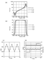
- FIG. 2 is a sectional view taken along line II-II of the elastic wave device of FIG. 1.
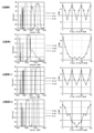
- FIG. 3A, FIG. 3B, and FIG. 3C are diagrams showing impedance characteristics, phase characteristics, and the difference between the resonance frequency and the anti-resonance frequency of the resonator according to the embodiment, respectively.
- FIG. 4A, FIG. 4B, FIG. 4C, and FIG. 4D are impedance characteristics, phase characteristics, resonance frequency, and the difference between the resonance frequency and the antiresonance frequency of the resonator according to the embodiment, respectively. It is a figure which shows and a maximum phase value.
- FIG. 5C are plan views showing arrangement examples of a plurality of resonators. It is a diagram which shows the characteristic of the resonator which concerns on a comparative example.
- FIG. 7A, FIG. 7B and FIG. 7C are diagrams corresponding to FIG. 3 when the thickness of the LN layer is different.
- 8A and 8B are diagrams showing impedance characteristics and phase characteristics of the resonator according to the embodiment.
- 9A and 9B are diagrams showing the impedance characteristic and the phase characteristic of the resonator according to the embodiment.
- 10A and 10B are diagrams showing the impedance characteristic and the phase characteristic of the resonator according to the embodiment. It is a circuit diagram which shows typically the structure of the duplexer as an example of utilization of the elastic wave apparatus of FIG.
- FIG. 14A and 14B are diagrams showing impedance characteristics and phase characteristics of the acoustic wave device shown in FIG. 13, respectively.
- 15(a), 15(b), and 15(c) are diagrams showing the resonance frequency, the difference between the resonance frequency and the anti-resonance frequency, and the maximum phase value of the acoustic wave device shown in FIG. 13, respectively.
- the acoustic wave device may be either upward or downward in any direction, but hereinafter, for convenience, an orthogonal coordinate system composed of the D1 axis, the D2 axis, and the D3 axis is defined and ,
- the term “upper surface” or “lower surface” may be used with the positive side of the D3 axis as the upper side.
- the term “planar view” or “planar see-through” means viewing in the D3 axis direction unless otherwise specified.
- the D1 axis is defined to be parallel to the propagation direction of elastic waves propagating along the upper surface of the LN layer described later, and the D2 axis is defined to be parallel to the upper surface of the LN layer and orthogonal to the D1 axis.
- the D3 axis is defined to be orthogonal to the upper surface of the LN layer.
- FIG. 1 is a plan view showing a configuration of a main part of the acoustic wave device 1.
- FIG. 2 is a sectional view taken along line II-II in FIG.
- the acoustic wave device 1 is located, for example, on the substrate 3 (FIG. 2), the multilayer film 5 (FIG. 2) located on the substrate 3, the LN layer 7 located on the multilayer film 5, and the LN layer 7. And a conductive layer 9.
- Each layer has, for example, a substantially constant thickness.
- the combination of the substrate 3, the multilayer film 5 and the LN layer 7 may be referred to as the fixed substrate 2 (FIG. 2).
- the acoustic wave device 1 when a voltage is applied to the conductive layer 9, the acoustic wave propagating in the LN layer 7 is excited.
- the elastic wave device 1 constitutes, for example, a resonator and/or a filter that uses this elastic wave.
- the multilayer film 5 contributes to, for example, reflecting elastic waves and confining the energy of the elastic waves in the LN layer 7.
- the substrate 3 contributes to reinforcing the strength of the multilayer film 5 and the LN layer 7, for example.
- the substrate 3 does not directly affect the electrical characteristics of the acoustic wave device 1, as will be understood from the description below. Therefore, the material and size of the substrate 3 may be set appropriately.
- the material of the substrate 3 is, for example, an insulating material, and the insulating material is, for example, resin or ceramic.
- the substrate 3 may be made of a material having a lower coefficient of thermal expansion than the LN layer 7 or the like. In this case, for example, it is possible to reduce the risk that the frequency characteristics of the acoustic wave device 1 will change due to temperature changes. Examples of such a material include a semiconductor such as silicon, a single crystal such as sapphire, and a ceramic such as an aluminum oxide sintered body.
- the substrate 3 may be configured by stacking a plurality of layers made of different materials. The thickness of the substrate 3 is thicker than that of the LN layer 7, for example.
- the multilayer film 5 includes a low sound velocity layer 11 made of a material having a lower sound velocity than the LN layer 7 such as silicon dioxide (SiO 2 ), and tantalum pentoxide (Ta 2 O 5 ), hafnium oxide (HfO 3 ), or the like.
- the LN layer 7 and the high sonic layer 13 made of a material having a higher sonic velocity are alternately laminated.
- the high sound velocity layer 13 has a higher acoustic impedance than the low sound velocity layer 11.
- the elastic wave reflectance is relatively high at the interface between the two.
- leakage of elastic waves propagating through the LN layer 7 is reduced.
- the number of laminated layers of the multilayer film 5 may be set appropriately.
- the total number of laminated layers of the low sound velocity layer 11 and the high sound velocity layer 13 may be 3 or more and 12 or less.
- the multilayer film 5 may be composed of a total of two layers, one low sound velocity layer 11 and one high sound velocity layer 13.
- the total number of laminated layers of the multilayer film 5 may be even or odd, but the layer in contact with the LN layer 7 is the low acoustic velocity layer 11.
- the layer in contact with the substrate 3 may be the low sound velocity layer 11 or the high sound velocity layer 13.
- an additional layer may be inserted between each layer for the purpose of adhesion and prevention of diffusion. In that case, there is no problem if the layer is thin enough not to affect the characteristics (approximately 0.01 ⁇ or less based on the wavelength ⁇ described later).
- the LN layer 7 is composed of a single crystal of lithium niobate (LiNbO 3 , LN).
- the cut angle of the LN layer 7 is, for example, Euler angles ( ⁇ , ⁇ , ⁇ ) (0° ⁇ 10°, ⁇ 25° or more and 15° or less, 0° or more and 360° or less).
- the thickness of the LN layer 7 is relatively thin, and is, for example, 0.3 ⁇ or less with respect to ⁇ .
- the conductive layer 9 is made of metal, for example.
- the metal may be of any suitable type, for example, aluminum (Al) or an alloy containing Al as a main component (Al alloy).
- the Al alloy is, for example, an aluminum-copper (Cu) alloy.
- the conductive layer 9 may be composed of a plurality of metal layers. For example, a relatively thin layer made of titanium (Ti) may be provided between Al or Al alloy and the LN layer 7 to enhance their bondability.
- the conductive layer 9 is formed so as to constitute the resonator 15 in the example of FIG.
- the resonator 15 is configured as a so-called 1-port elastic wave resonator, and when an electric signal of a predetermined frequency is input from one of the terminals 17A and 17B which are conceptually and schematically shown, resonance is caused and the resonance is generated. The generated signal can be output from the other terminal 17A and 17B.
- the conductive layer 9 (resonator 15) includes, for example, an IDT electrode 19 and a pair of reflectors 21 located on both sides of the IDT electrode 19.
- the IDT electrode 19 includes a pair of comb-teeth electrodes 23. Note that one comb-tooth electrode 23 is hatched to improve visibility. Each comb-tooth electrode 23 includes, for example, a bus bar 25, a plurality of electrode fingers 27 extending from the bus bar 25 in parallel with each other, and a dummy electrode 29 protruding from the bus bar 25 between the plurality of electrode fingers 27. The pair of comb-teeth electrodes 23 are arranged so that the plurality of electrode fingers 27 are engaged with each other (intersecting).
- the bus bar 25 is, for example, formed in a long shape having a substantially constant width and linearly extending in the propagation direction of the elastic wave (the direction in which the electrode fingers 27 are repeatedly arranged, in this example, the D1 axis direction).
- the pair of bus bars 25 are opposed to each other in the direction (D2 axis direction) orthogonal to the elastic wave propagation direction.
- the bus bar 25 may have a changed width or may be inclined with respect to the propagation direction of the elastic wave.
- Each electrode finger 27 is, for example, formed in an elongated shape having a substantially constant width and extending linearly in a direction (D2 axis direction) orthogonal to the elastic wave propagation direction.
- the plurality of electrode fingers 27 are arranged in the elastic wave propagation direction. Further, the plurality of electrode fingers 27 of the one comb-teeth electrode 23 and the plurality of electrode fingers 27 of the other comb-teeth electrode 23 are basically arranged alternately.
- the pitch p of the plurality of electrode fingers 27 (for example, the distance between the centers of two electrode fingers 27 adjacent to each other) is basically constant in the IDT electrode 19. It should be noted that a part of the IDT electrode 19 may be provided with a narrow pitch part in which the pitch p is narrower than the other part, or a wide pitch part in which the pitch p is wider than the other part.
- the pitch p is the pitch of the portion (most of the plurality of electrode fingers 27) excluding the peculiar portion such as the narrow pitch portion or the wide pitch portion as described above unless otherwise specified. Shall be said. Also, in the case where the pitches of most of the plurality of electrode fingers 27 except for the peculiar portion are changed, the average value of the pitches of most of the plurality of electrode fingers 27 is set as the value of pitch p. May be used. Therefore, a value twice the pitch p is set as the wavelength ⁇ .
- the number of electrode fingers 27 may be appropriately set according to the electrical characteristics required of the resonator 15. Since FIG. 2 is a schematic diagram, the number of electrode fingers 27 is shown small. The same applies to the strip electrode 33 of the reflector 21 described later.
- the lengths and widths of the plurality of electrode fingers 27 may be appropriately set according to required electrical characteristics and the like.
- the dummy electrode 29 has, for example, a substantially constant width and projects in a direction orthogonal to the propagation direction of the elastic wave.
- the plurality of dummy electrodes 29 are arranged at the same pitch as the plurality of electrode fingers 27, and the tip of the dummy electrode 29 of the one comb-teeth electrode 23 is separated from the tip of the electrode finger 27 of the other comb-teeth electrode 23 by a gap. Are facing through.
- the IDT electrode 19 may not include the dummy electrode 29.
- the pair of reflectors 21 are located on both sides of the plurality of IDT electrodes 19 in the acoustic wave propagation direction.
- the reflector 21 includes a pair of bus bars 31 facing each other and a plurality of strip electrodes 33 extending between the pair of bus bars 31.
- the upper surface of the LN layer 7 may be covered with a protective film made of SiO 2 , Si 3 N 4 or the like from above the conductive layer 9.
- the protective film may be a laminate of a plurality of layers made of these materials. The protective film may simply prevent corrosion of the conductive layer 9 or may contribute to temperature compensation.
- an additional film made of an insulator or a metal may be provided on the upper surface or the lower surface of the IDT electrode 19 and the reflector 21 in order to improve the reflection coefficient of elastic waves.
- the configurations shown in FIGS. 1 and 2 may be packaged appropriately.
- the package may be, for example, one in which the configuration shown in the figure is mounted on a substrate (not shown) such that the upper surfaces of the LN layers 7 face each other with a gap therebetween, and resin sealing is performed from above. It may be a wafer level package type in which a box-shaped cover is provided on the top.
- the LN layer 7 is relatively thin, and its Euler angles ( ⁇ , ⁇ , ⁇ ) are (0° ⁇ 10°, ⁇ 25° to 15°, 0° to 360°).
- Modal elastic waves are available.
- the propagation velocity (sound velocity) of the elastic wave in the slab mode is higher than the propagation velocity of a general SAW (Surface Acoustic Wave).
- the propagation speed of a general SAW is 3000 to 4000 m/s, while the propagation speed of elastic waves in the slab mode is 10000 m/s or more. Therefore, it is possible to realize resonance in a high frequency region as compared with the related art with the pitch p equal to that of the related art.
- a resonance frequency (fr) of 5 GHz or higher can be realized with a pitch p of 1 ⁇ m or higher.
- the inventor of the present application variously changes the material and thickness of the multilayer film 5, the Euler angle of the piezoelectric layer (LN layer 7 in the present embodiment), the material and thickness, and the thickness of the conductive layer 9 to obtain the elastic wave.
- a simulation calculation was performed on the frequency characteristics of the device 1. Then, the inventors have found conditions that can realize resonance in a relatively high frequency region (for example, 5 GHz or more) by using elastic waves in the slab mode. Specifically, it is as follows.
- the Euler angle of the LN layer 7 is swung to perform a simulation, and resonance in a relatively high high frequency region can be realized, and the Euler angle of the LN layer 7 where spurious does not exist near fr and the anti-resonance frequency (fa) is obtained.
- the LN layer 7 has a thickness of 0.1875 ⁇
- the low sound velocity layer 11 has a thickness of 0.09 ⁇
- the high sound velocity layer 13 has a thickness of 0.07 ⁇
- the conductive layer 9 has a thickness of 0.06 ⁇
- the pitch p is 1 ⁇ m
- Duty0 It is set to 0.5.
- FIGS. 3(a) to 3(c) 3A is an impedance characteristic
- FIG. 3B is a phase characteristic
- FIG. 3C is a diagram showing how the difference ( ⁇ f) between fr and fa changes when ⁇ is changed. is there.
- the horizontal axis represents frequency
- the vertical axis represents absolute value of impedance in FIG. 3A
- FIG. 3B represents phase
- the horizontal axis represents ⁇ and the vertical axis represents ⁇ f.
- FIG. 4(a) shows impedance characteristics
- FIG. 4(b) shows phase characteristics
- FIG. 4(c) shows fr
- FIG. 4(d) shows ⁇ f and the maximum phase value (MaxPhase) between fr and fa. Is shown.
- a plurality of resonators 15 shown in FIG. 1 may be provided and the propagation angles (directions of repeated arrangement of electrode fingers) may be different from each other.
- the propagation angle of the series resonator may be different from the propagation angle of the parallel resonator.
- the propagation angle of the series resonator is set to any of 15° to 45°, 75° to 105°, 135° to 165°, 195° to 225°, 255° to 285°, and 315° to 345°.
- the propagation angles of the parallel resonators are -15° (345°) to 15°, 45° to 75°, 105° to 135°, 165° to 195°, 225° to 255°, 285° to 315°. Good.
- the upper limit and the lower limit are included in the angular range of the series resonator, and the upper limit and the lower limit are not included in the angular range of the parallel resonator.
- the propagation angle of the series resonator is 20°+60° ⁇ n1 or more and 40°+60° ⁇ n1 or less, and the propagation angle of the parallel resonator is ⁇ 10°+60° ⁇ n2 or more 10°+60° ⁇ n2. It may be as follows. Hereinafter, the propagation angle may be represented by ⁇ .
- the fr can be changed by the difference in the propagation angle, which facilitates the design. For example, fr can be further moved to the higher frequency side without reducing the pitch p.
- the thickness of the LN layer 7 and the thickness of each layer of the multilayer film 5 are optimized by the pitch p of the electrode fingers 27, the pitch p of each resonator 15 is set even when there are a plurality of resonators 15 having different fr. Since they can be brought close to each other, a high-performance acoustic wave device can be provided.
- the series resonator 15S (first resonator) is arranged so that ⁇ is 90°
- the parallel resonator 15P (second resonator) is ⁇ .
- the series resonator 15S is arranged so that ⁇ is 30° and 90°
- the parallel resonator 15P is arranged so that ⁇ is 0° and 60°. Good. In this case, the degree of freedom of layout is further increased.
- the propagation angle is different between the series resonator 15S and the parallel resonator 15P, but the propagation angle may be different between the series resonators and the parallel resonators.
- fr may be made different between series resonators and parallel resonators in order to improve the shoulder characteristics of the filter and to adjust the out-of-band attenuation characteristics.
- the propagation angle may be used for this adjustment.
- Fig. 5(c) shows the case where the propagation angle ( ⁇ ) is made different between the series resonators.
- the first series resonator 15S1 (first resonator) and the second series resonator 15S2 (second resonator) may be present in the series resonator 15S.
- resonators having the same pitch and different fr can be realized. For example, it is possible to suppress a decrease in the power resistance due to the pitch becoming small and the electric power being concentrated in a specific resonator. be able to.
- adjacent resonators means that other resonators are not located between the resonators, and the directions in which they are adjacent are not limited.
- the propagation angle is made different between the resonators located on the extension line of the propagation direction, the above effect is enhanced.
- the resonator 15 is shown in a rectangular shape, and the long side indicates the propagation direction.
- the propagation direction in each resonator that is, the direction in which the electrode fingers are repeatedly arranged may be indicated by an arrow in a rectangle representing the resonator.
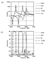
- Comparative Example 1 a resonator having the same configuration as that of the above-described embodiment except that a thick LN substrate was used as the LN layer 7 and the multilayer film 5 was not provided, and the characteristics were measured with different propagation angles.
- Comparative Example 2 a resonator having a configuration in which the Euler angle of the LN substrate was changed to (0, 38, ⁇ ) from Comparative Example 1 was made, and the characteristics were measured with different propagation angles.
- the Euler angle corresponds to the cut angle generally used for the LN substrate.
- Comparative Example 1-2 a resonator having a configuration in which the thickness of the LN substrate of Comparative Example 1 was 0.5 ⁇ and the Si substrate was arranged on the lower surface of the resonator was measured, and the characteristics were measured with different propagation angles.
- Comparative Example 2-2 a resonator having a configuration in which the thickness of the LN substrate of Comparative Example 2 was 0.5 ⁇ and the Si substrate was arranged on the lower surface thereof was prepared, and the characteristics were measured with different propagation angles. ..
- FIG. 6 is a diagram showing the correlation between the phase characteristics and the propagation angle and the correlation between ⁇ f and the propagation angle of Comparative Examples 1, 1-2, 2 and 2-1.
- no elastic wave in the slab mode could be confirmed, and it was confirmed that the resonance frequency was in the 2 MHz range. That is, it was confirmed that the types of elastic waves handled were different from those of the above-described embodiment.
- FIG. 7 is a diagram corresponding to FIG. 3 when the thickness of the LN layer is changed.
- the thickness of the LN layer 7 may be 0.1175 ⁇ or more and 0.22 ⁇ or less. The characteristics shown in FIG. 3 are obtained by setting the thickness of the LN layer 7 to 0.1875 ⁇ .
- FIG. 8A and 8B show simulation results when the thickness of the high sonic layer 13 is set to 0.07 ⁇ and the thickness of the low sonic layer 11 is changed.
- FIG. 8A shows impedance characteristics
- FIG. 8B shows phase characteristics.
- the horizontal axis represents the frequency
- the vertical axis represents the absolute value of impedance in FIG. 8A
- the phase in FIG. 8B is shown.
- the thickness of the low sound velocity layer 11 may be 0.065 ⁇ or more and 0.1375 ⁇ or less.
- FIGS. 9A and 9B show the simulation results when the thickness of the low sonic layer 11 is set to 0.09 ⁇ and the thickness of the high sonic layer 13 is changed.
- 9A and 9B are diagrams corresponding to FIGS. 8A and 8B.
- the thickness of the high sound velocity layer 13 may be 0.055 ⁇ or more and 0.1175 ⁇ or less.
- the surface roughness of each layer constituting the multilayer film 5 may be increased as the LN layer 7 approaches the substrate 3. More specifically, the surface roughness of the layer in contact with the LN layer 7 in the low acoustic velocity layer 11 is smaller than that of the layer located closest to the substrate 3 side. With such a configuration, the bulk wave transmitted from the LN layer 3 can be scattered.
- FIGS. 10A and 10B are diagrams corresponding to FIGS. 9A and 9B, respectively.
- the conductive layer 9 may have a thickness of 0.01 ⁇ or more and 0.0875 ⁇ or less.
- the acoustic wave device 1 may be manufactured by combining various known processes.
- the low acoustic velocity layer 11 and the high acoustic velocity layer 13 are sequentially formed on the wafer to be the substrate 3 by a thin film forming method such as CVD (chemical vapor deposition).
- a wafer to be the LN layer 7 is prepared by the same manufacturing process as that for a general LN substrate wafer.
- the wafer to be the LN layer 7 is attached to the wafer to be the substrate 3 and the multilayer film 5.
- the LN layer 7 is brought into direct contact with the uppermost layer (eg, SiO 2 layer) of the multilayer film 5.
- Heat treatment or the like may be performed before or after the contact. After that, a metal layer to be the conductive layer 9 is formed and patterned on the upper surface of the wafer to be the LN layer 7, and the wafer is diced. Thereby, the acoustic wave device 1 is manufactured. Of course, appropriate steps may be added depending on the form of the package.
- an acoustic wave device 1A that does not include a multilayer film may be used.
- the acoustic wave device 1A is similar to the acoustic wave device 1 in that the LN layer 7 is supported by the substrate 3, but there is no multilayer film 5 and the region where the IDT electrode 19 is located in the LN layer 7 and the substrate 3 are separated. It has a membrane shape with voids in between. This void allows the elastic wave to be confined in the LN layer 7.
- a concave portion 3 a is formed on the upper surface of the substrate 3.
- the LN layer 7 is directly or indirectly bonded to the substrate 3 so that the recess 3a and the IDT electrode 19 overlap each other in a top view.
- the basic configuration of the acoustic wave device 1A is that the Euler angle of the LN layer 7 is (0, 0, ⁇ ), the thickness of the LN layer 7 is 0.185 ⁇ , the thickness of the conductive layer 9 is 0.065 ⁇ , the pitch p is 1 ⁇ m, and Duty0. It is set to 0.5.
- FIGS. 15A, 15B, and 15C show fr, ⁇ f, and maximum phase value when ⁇ is changed.
- the dyne back wave device 1A like the elastic wave device 1, does not change fr, ⁇ f, and maximum phase value even when ⁇ (propagation angle) is changed. It was confirmed that there was little fluctuation.
- the example shown in FIG. 13 has a configuration in which the substrate 3 is provided with a recess, but the configuration is not limited to this.
- a convex portion functioning as a spacer may be provided on the upper surface of the substrate 3 having a flat upper surface, and the LN layer may be arranged on the convex portion.
- the convex portion may be formed of a material different from that of the substrate 3.
- the recess 3a may be provided with one recess 3a for one resonator, or may be provided with a recess 3a for withstanding a plurality of resonators.
- the material of the substrate 3 is not particularly limited, but a Si substrate may be used in consideration of workability.
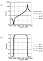
- FIG. 11 is a circuit diagram schematically showing the configuration of the duplexer 101 as an example of using the elastic wave device 1.
- the comb-teeth electrode 23 is schematically shown in this figure by a forked shape of a fork, and the reflector 21 is a single line bent at both ends. It is represented by.
- the demultiplexer 101 filters, for example, a transmission signal from the transmission terminal 105 and outputs it to the antenna terminal 103, and a reception signal from the antenna terminal 103 and outputs it to a pair of reception terminals 107. It has a reception filter 111.
- the transmission filter 109 is composed of, for example, a ladder type filter in which a plurality of resonators 15 are connected in a ladder type. That is, the transmission filter 109 connects a plurality (or one) of the resonators 15 connected in series between the transmission terminal 105 and the antenna terminal 103, the series line (series arm) thereof, and the reference potential. A plurality of (even one is possible) resonators 15 (parallel arms). The plurality of resonators 15 that form the transmission filter 109 are provided, for example, on the same fixed substrate 2 (3, 5, and 7).
- the reception filter 111 includes, for example, a resonator 15 and a multimode type filter (including a double mode type filter) 113.
- the multimode filter 113 has a plurality of (three in the illustrated example) IDT electrodes 19 arranged in the propagation direction of the elastic wave, and a pair of reflectors 21 arranged on both sides thereof.
- the resonator 15 and the multimode filter 113 that form the reception filter 111 are provided on the same fixed substrate 2, for example.
- the transmission filter 109 and the reception filter 111 may be provided on the same fixed substrate 2 or different fixed substrates 2.
- FIG. 11 is merely an example of the configuration of the demultiplexer 101, and the reception filter 111 may be configured by a ladder type filter like the transmission filter 109, for example.
- the demultiplexer 101 includes the transmission filter 109 and the reception filter 111 has been described, but the demultiplexer 101 is not limited to this. For example, it may be a diplexer or a multiplexer including three or more filters.
- FIG. 12 is a block diagram showing a main part of a communication device 151 as an example of using the elastic wave device 1 (branching filter 101).
- the communication device 151 performs wireless communication using radio waves and includes the duplexer 101.
- the transmission information signal TIS including the information to be transmitted is modulated by the RF-IC (Radio Frequency Integrated Circuit) 153 and the frequency is raised (conversion of the carrier frequency to a high frequency signal) to form a transmission signal TS.
- the transmission signal TS has unnecessary components other than the transmission pass band removed by the band pass filter 155, is amplified by the amplifier 157, and is input to the demultiplexer 101 (transmission terminal 105). Then, the demultiplexer 101 (transmission filter 109) removes unnecessary components other than the transmission pass band from the input transmission signal TS, and outputs the removed transmission signal TS from the antenna terminal 103 to the antenna 159. ..
- the antenna 159 converts the input electric signal (transmission signal TS) into a radio signal (radio wave) and transmits it.
- a radio signal (radio wave) received by the antenna 159 is converted into an electric signal (received signal RS) by the antenna 159 and input to the duplexer 101 (antenna terminal 103).
- the demultiplexer 101 removes unnecessary components other than the reception pass band from the input reception signal RS and outputs it from the reception terminal 107 to the amplifier 161.
- the output reception signal RS is amplified by the amplifier 161, and unnecessary components other than the reception pass band are removed by the band pass filter 163. Then, the reception signal RS is subjected to frequency reduction and demodulation by the RF-IC 153 to be a reception information signal RIS.
- the transmission information signal TIS and the reception information signal RIS may be low-frequency signals (baseband signals) containing appropriate information, and are, for example, analog voice signals or digitized voice signals.
- the pass band of the radio signal may be set appropriately, and in the present embodiment, a pass band of relatively high frequency (for example, 5 GHz or more) is also possible.
- the modulation method may be phase modulation, amplitude modulation, frequency modulation, or a combination of two or more of these.
- the direct conversion method is illustrated in FIG. 12 as the circuit method, any other suitable circuit method may be used, and for example, a double superheterodyne method may be used.
- FIG. 12 schematically shows only a main part, and a low-pass filter, an isolator or the like may be added at an appropriate position, or a position of an amplifier or the like may be changed.
- the present invention is not limited to the above embodiment and may be implemented in various modes.
- the thickness of each layer and the Euler angle of the LN layer may be values outside the range exemplified in the embodiment.
Landscapes
- Physics & Mathematics (AREA)
- Acoustics & Sound (AREA)
- Chemical & Material Sciences (AREA)
- Crystallography & Structural Chemistry (AREA)
- Engineering & Computer Science (AREA)
- Materials Engineering (AREA)
- Surface Acoustic Wave Elements And Circuit Networks Thereof (AREA)
Priority Applications (3)
| Application Number | Priority Date | Filing Date | Title |
|---|---|---|---|
| JP2020550191A JP6856825B2 (ja) | 2018-12-21 | 2019-12-20 | 弾性波装置、分波器および通信装置 |
| US17/414,778 US20220069803A1 (en) | 2018-12-21 | 2019-12-20 | Elastic wave device, splitter, and communication apparatus |
| CN201980082801.8A CN113302840A (zh) | 2018-12-21 | 2019-12-20 | 弹性波装置、分波器以及通信装置 |
Applications Claiming Priority (2)
| Application Number | Priority Date | Filing Date | Title |
|---|---|---|---|
| JP2018239125 | 2018-12-21 | ||
| JP2018-239125 | 2018-12-21 |
Publications (1)
| Publication Number | Publication Date |
|---|---|
| WO2020130128A1 true WO2020130128A1 (ja) | 2020-06-25 |
Family
ID=71101295
Family Applications (1)
| Application Number | Title | Priority Date | Filing Date |
|---|---|---|---|
| PCT/JP2019/050045 WO2020130128A1 (ja) | 2018-12-21 | 2019-12-20 | 弾性波装置、分波器および通信装置 |
Country Status (4)
| Country | Link |
|---|---|
| US (1) | US20220069803A1 (zh) |
| JP (1) | JP6856825B2 (zh) |
| CN (1) | CN113302840A (zh) |
| WO (1) | WO2020130128A1 (zh) |
Cited By (13)
| Publication number | Priority date | Publication date | Assignee | Title |
|---|---|---|---|---|
| JP6935573B1 (ja) * | 2020-12-23 | 2021-09-15 | 日本碍子株式会社 | 複合基板および弾性表面波素子 |
| WO2021187537A1 (ja) * | 2020-03-18 | 2021-09-23 | 株式会社村田製作所 | 弾性波装置 |
| WO2022054372A1 (ja) * | 2020-09-10 | 2022-03-17 | 日本碍子株式会社 | 弾性波デバイス用複合基板 |
| WO2022054773A1 (ja) * | 2020-09-09 | 2022-03-17 | 株式会社村田製作所 | 弾性波装置 |
| WO2022059759A1 (ja) * | 2020-09-16 | 2022-03-24 | 株式会社村田製作所 | 弾性波装置 |
| WO2022075415A1 (ja) * | 2020-10-08 | 2022-04-14 | 株式会社村田製作所 | 弾性波装置 |
| WO2022138457A1 (ja) * | 2020-12-23 | 2022-06-30 | 株式会社村田製作所 | 弾性波装置 |
| WO2023033032A1 (ja) * | 2021-08-31 | 2023-03-09 | 京セラ株式会社 | 弾性波素子、分波器および通信装置 |
| WO2023058713A1 (ja) * | 2021-10-07 | 2023-04-13 | 株式会社村田製作所 | 弾性波素子の製造方法および弾性波素子 |
| WO2023145878A1 (ja) * | 2022-01-27 | 2023-08-03 | 株式会社村田製作所 | 弾性波装置 |
| WO2024014204A1 (ja) * | 2022-07-13 | 2024-01-18 | 株式会社村田製作所 | 弾性波装置 |
| WO2024043343A1 (ja) * | 2022-08-26 | 2024-02-29 | 株式会社村田製作所 | 弾性波装置 |
| WO2024128164A1 (ja) * | 2022-12-12 | 2024-06-20 | 京セラ株式会社 | 弾性波装置、フィルタ、および通信装置 |
Families Citing this family (1)
| Publication number | Priority date | Publication date | Assignee | Title |
|---|---|---|---|---|
| WO2020116528A1 (ja) * | 2018-12-06 | 2020-06-11 | 株式会社村田製作所 | 弾性波装置 |
Citations (8)
| Publication number | Priority date | Publication date | Assignee | Title |
|---|---|---|---|---|
| WO2005069485A1 (ja) * | 2004-01-13 | 2005-07-28 | Murata Manufacturing Co., Ltd. | 弾性境界波装置 |
| JP2009290914A (ja) * | 2003-12-16 | 2009-12-10 | Murata Mfg Co Ltd | 弾性境界波装置 |
| JP2010220204A (ja) * | 2009-02-17 | 2010-09-30 | Ngk Insulators Ltd | ラム波装置 |
| JP2010278830A (ja) * | 2009-05-29 | 2010-12-09 | Murata Mfg Co Ltd | ラダー型フィルタ及びその製造方法並びにデュプレクサ |
| WO2012086441A1 (ja) * | 2010-12-24 | 2012-06-28 | 株式会社村田製作所 | 弾性波装置及びその製造方法 |
| JP2016140110A (ja) * | 2013-10-31 | 2016-08-04 | 京セラ株式会社 | 弾性波素子、フィルタ素子および通信装置 |
| WO2016129662A1 (ja) * | 2015-02-13 | 2016-08-18 | 京セラ株式会社 | 弾性波装置、分波器および通信装置 |
| WO2018154950A1 (ja) * | 2017-02-21 | 2018-08-30 | 株式会社村田製作所 | 弾性波装置、高周波フロントエンド回路及び通信装置 |
Family Cites Families (12)
| Publication number | Priority date | Publication date | Assignee | Title |
|---|---|---|---|---|
| JP4553047B2 (ja) * | 2008-03-12 | 2010-09-29 | セイコーエプソン株式会社 | ラム波型共振子及び発振器 |
| WO2010001522A1 (ja) * | 2008-06-30 | 2010-01-07 | 株式会社村田製作所 | 帯域阻止フィルタ |
| CN102089970A (zh) * | 2008-07-11 | 2011-06-08 | 松下电器产业株式会社 | 板波元件和使用该板波元件的电子设备 |
| JP5176863B2 (ja) * | 2008-10-21 | 2013-04-03 | 株式会社村田製作所 | 弾性波装置 |
| JP5601377B2 (ja) * | 2010-11-30 | 2014-10-08 | 株式会社村田製作所 | 弾性波装置及びその製造方法 |
| WO2013080461A1 (ja) * | 2011-11-30 | 2013-06-06 | パナソニック株式会社 | ラダー型弾性波フィルタと、これを用いたアンテナ共用器 |
| WO2016052129A1 (ja) * | 2014-09-30 | 2016-04-07 | 株式会社村田製作所 | 弾性波装置及びその製造方法 |
| CN107852144B (zh) * | 2015-10-30 | 2021-12-10 | 京瓷株式会社 | 弹性波谐振器、弹性波滤波器、分波器、通信装置以及弹性波谐振器的设计方法 |
| JP2018056630A (ja) * | 2016-09-26 | 2018-04-05 | 株式会社村田製作所 | 弾性波装置、高周波フロントエンド回路及び通信装置 |
| JP2018182615A (ja) * | 2017-04-18 | 2018-11-15 | 株式会社村田製作所 | 弾性波装置 |
| CN110582938B (zh) * | 2017-04-26 | 2023-06-23 | 株式会社村田制作所 | 弹性波装置 |
| KR102329740B1 (ko) * | 2017-09-27 | 2021-11-22 | 가부시키가이샤 무라타 세이사쿠쇼 | 탄성파 장치 |
-
2019
- 2019-12-20 CN CN201980082801.8A patent/CN113302840A/zh active Pending
- 2019-12-20 JP JP2020550191A patent/JP6856825B2/ja active Active
- 2019-12-20 WO PCT/JP2019/050045 patent/WO2020130128A1/ja active Application Filing
- 2019-12-20 US US17/414,778 patent/US20220069803A1/en active Pending
Patent Citations (8)
| Publication number | Priority date | Publication date | Assignee | Title |
|---|---|---|---|---|
| JP2009290914A (ja) * | 2003-12-16 | 2009-12-10 | Murata Mfg Co Ltd | 弾性境界波装置 |
| WO2005069485A1 (ja) * | 2004-01-13 | 2005-07-28 | Murata Manufacturing Co., Ltd. | 弾性境界波装置 |
| JP2010220204A (ja) * | 2009-02-17 | 2010-09-30 | Ngk Insulators Ltd | ラム波装置 |
| JP2010278830A (ja) * | 2009-05-29 | 2010-12-09 | Murata Mfg Co Ltd | ラダー型フィルタ及びその製造方法並びにデュプレクサ |
| WO2012086441A1 (ja) * | 2010-12-24 | 2012-06-28 | 株式会社村田製作所 | 弾性波装置及びその製造方法 |
| JP2016140110A (ja) * | 2013-10-31 | 2016-08-04 | 京セラ株式会社 | 弾性波素子、フィルタ素子および通信装置 |
| WO2016129662A1 (ja) * | 2015-02-13 | 2016-08-18 | 京セラ株式会社 | 弾性波装置、分波器および通信装置 |
| WO2018154950A1 (ja) * | 2017-02-21 | 2018-08-30 | 株式会社村田製作所 | 弾性波装置、高周波フロントエンド回路及び通信装置 |
Cited By (15)
| Publication number | Priority date | Publication date | Assignee | Title |
|---|---|---|---|---|
| WO2021187537A1 (ja) * | 2020-03-18 | 2021-09-23 | 株式会社村田製作所 | 弾性波装置 |
| WO2022054773A1 (ja) * | 2020-09-09 | 2022-03-17 | 株式会社村田製作所 | 弾性波装置 |
| WO2022054372A1 (ja) * | 2020-09-10 | 2022-03-17 | 日本碍子株式会社 | 弾性波デバイス用複合基板 |
| WO2022059759A1 (ja) * | 2020-09-16 | 2022-03-24 | 株式会社村田製作所 | 弾性波装置 |
| WO2022075415A1 (ja) * | 2020-10-08 | 2022-04-14 | 株式会社村田製作所 | 弾性波装置 |
| WO2022138457A1 (ja) * | 2020-12-23 | 2022-06-30 | 株式会社村田製作所 | 弾性波装置 |
| JP6935573B1 (ja) * | 2020-12-23 | 2021-09-15 | 日本碍子株式会社 | 複合基板および弾性表面波素子 |
| WO2022137646A1 (ja) * | 2020-12-23 | 2022-06-30 | 日本碍子株式会社 | 複合基板および弾性表面波素子 |
| JP2022099722A (ja) * | 2020-12-23 | 2022-07-05 | 日本碍子株式会社 | 複合基板および弾性表面波素子 |
| WO2023033032A1 (ja) * | 2021-08-31 | 2023-03-09 | 京セラ株式会社 | 弾性波素子、分波器および通信装置 |
| WO2023058713A1 (ja) * | 2021-10-07 | 2023-04-13 | 株式会社村田製作所 | 弾性波素子の製造方法および弾性波素子 |
| WO2023145878A1 (ja) * | 2022-01-27 | 2023-08-03 | 株式会社村田製作所 | 弾性波装置 |
| WO2024014204A1 (ja) * | 2022-07-13 | 2024-01-18 | 株式会社村田製作所 | 弾性波装置 |
| WO2024043343A1 (ja) * | 2022-08-26 | 2024-02-29 | 株式会社村田製作所 | 弾性波装置 |
| WO2024128164A1 (ja) * | 2022-12-12 | 2024-06-20 | 京セラ株式会社 | 弾性波装置、フィルタ、および通信装置 |
Also Published As
| Publication number | Publication date |
|---|---|
| US20220069803A1 (en) | 2022-03-03 |
| JPWO2020130128A1 (ja) | 2021-02-15 |
| CN113302840A (zh) | 2021-08-24 |
| JP6856825B2 (ja) | 2021-04-14 |
Similar Documents
| Publication | Publication Date | Title |
|---|---|---|
| JP6856825B2 (ja) | 弾性波装置、分波器および通信装置 | |
| JP7433268B2 (ja) | 弾性波装置、分波器および通信装置 | |
| JP7278305B2 (ja) | 弾性波装置、分波器および通信装置 | |
| JP6806907B2 (ja) | 弾性波装置、分波器および通信装置 | |
| JP6854891B2 (ja) | 弾性波装置、分波器および通信装置 | |
| CN107204750B (zh) | 声波器件 | |
| JPWO2005086345A1 (ja) | 弾性境界波装置 | |
| JP6994855B2 (ja) | 弾性波素子、分波器および通信装置 | |
| JP6626904B2 (ja) | 弾性波素子および通信装置 | |
| US11863155B2 (en) | Surface acoustic wave element | |
| WO2022045307A1 (ja) | 弾性波素子及び通信装置 | |
| JP2019201345A (ja) | 弾性波共振器、フィルタおよびマルチプレクサ | |
| JPWO2019082806A1 (ja) | 弾性波素子 | |
| JP2020043403A (ja) | 弾性波共振器、フィルタおよびマルチプレクサ | |
| TW201939889A (zh) | 用於表面聲波濾波裝置中源抑制的轉換器結構 | |
| JP2019192994A (ja) | 弾性波共振器、フィルタおよびマルチプレクサ | |
| JP2019180064A (ja) | 弾性波フィルタ、分波器および通信装置 | |
| WO2021020102A1 (ja) | 弾性波装置及び通信装置 | |
| JP7037439B2 (ja) | 弾性波素子、分波器および通信装置 | |
| WO2024034528A1 (ja) | 弾性波装置、複合フィルタ及び通信装置 | |
| WO2023286704A1 (ja) | 弾性波装置、フィルタ、分波器及び通信装置 |
Legal Events
| Date | Code | Title | Description |
|---|---|---|---|
| 121 | Ep: the epo has been informed by wipo that ep was designated in this application |
Ref document number: 19901338 Country of ref document: EP Kind code of ref document: A1 |
|
| ENP | Entry into the national phase |
Ref document number: 2020550191 Country of ref document: JP Kind code of ref document: A |
|
| NENP | Non-entry into the national phase |
Ref country code: DE |
|
| 122 | Ep: pct application non-entry in european phase |
Ref document number: 19901338 Country of ref document: EP Kind code of ref document: A1 |