WO2023286704A1 - 弾性波装置、フィルタ、分波器及び通信装置 - Google Patents
弾性波装置、フィルタ、分波器及び通信装置 Download PDFInfo
- Publication number
- WO2023286704A1 WO2023286704A1 PCT/JP2022/027079 JP2022027079W WO2023286704A1 WO 2023286704 A1 WO2023286704 A1 WO 2023286704A1 JP 2022027079 W JP2022027079 W JP 2022027079W WO 2023286704 A1 WO2023286704 A1 WO 2023286704A1
- Authority
- WO
- WIPO (PCT)
- Prior art keywords
- electrode
- elastic wave
- electrode fingers
- region
- filter
- Prior art date
Links
- 238000004891 communication Methods 0.000 title claims description 13
- 230000005540 biological transmission Effects 0.000 claims description 27
- 239000000758 substrate Substances 0.000 description 56
- 239000011295 pitch Substances 0.000 description 35
- 239000000463 material Substances 0.000 description 28
- 238000010586 diagram Methods 0.000 description 24
- 239000004020 conductor Substances 0.000 description 21
- 230000000052 comparative effect Effects 0.000 description 16
- 230000000694 effects Effects 0.000 description 15
- 239000012528 membrane Substances 0.000 description 14
- 244000126211 Hericium coralloides Species 0.000 description 6
- VYPSYNLAJGMNEJ-UHFFFAOYSA-N Silicium dioxide Chemical compound O=[Si]=O VYPSYNLAJGMNEJ-UHFFFAOYSA-N 0.000 description 6
- 238000004088 simulation Methods 0.000 description 6
- 229910004298 SiO 2 Inorganic materials 0.000 description 5
- 238000004364 calculation method Methods 0.000 description 5
- 230000008859 change Effects 0.000 description 5
- 230000001902 propagating effect Effects 0.000 description 5
- 239000010936 titanium Substances 0.000 description 5
- 229910000838 Al alloy Inorganic materials 0.000 description 4
- 235000019687 Lamb Nutrition 0.000 description 4
- 238000006243 chemical reaction Methods 0.000 description 4
- 230000001681 protective effect Effects 0.000 description 4
- 239000013078 crystal Substances 0.000 description 3
- 229910052751 metal Inorganic materials 0.000 description 3
- 239000002184 metal Substances 0.000 description 3
- 238000000034 method Methods 0.000 description 3
- 229910045601 alloy Inorganic materials 0.000 description 2
- 239000000956 alloy Substances 0.000 description 2
- 229910052782 aluminium Inorganic materials 0.000 description 2
- 239000010949 copper Substances 0.000 description 2
- 239000000395 magnesium oxide Substances 0.000 description 2
- CPLXHLVBOLITMK-UHFFFAOYSA-N magnesium oxide Inorganic materials [Mg]=O CPLXHLVBOLITMK-UHFFFAOYSA-N 0.000 description 2
- AXZKOIWUVFPNLO-UHFFFAOYSA-N magnesium;oxygen(2-) Chemical compound [O-2].[Mg+2] AXZKOIWUVFPNLO-UHFFFAOYSA-N 0.000 description 2
- TWNQGVIAIRXVLR-UHFFFAOYSA-N oxo(oxoalumanyloxy)alumane Chemical compound O=[Al]O[Al]=O TWNQGVIAIRXVLR-UHFFFAOYSA-N 0.000 description 2
- 230000002787 reinforcement Effects 0.000 description 2
- 230000004044 response Effects 0.000 description 2
- 235000012239 silicon dioxide Nutrition 0.000 description 2
- 239000000377 silicon dioxide Substances 0.000 description 2
- 230000005236 sound signal Effects 0.000 description 2
- 238000010897 surface acoustic wave method Methods 0.000 description 2
- 229910052719 titanium Inorganic materials 0.000 description 2
- WSMQKESQZFQMFW-UHFFFAOYSA-N 5-methyl-pyrazole-3-carboxylic acid Chemical compound CC1=CC(C(O)=O)=NN1 WSMQKESQZFQMFW-UHFFFAOYSA-N 0.000 description 1
- 229910018072 Al 2 O 3 Inorganic materials 0.000 description 1
- 229910013641 LiNbO 3 Inorganic materials 0.000 description 1
- 229910052581 Si3N4 Inorganic materials 0.000 description 1
- XUIMIQQOPSSXEZ-UHFFFAOYSA-N Silicon Chemical compound [Si] XUIMIQQOPSSXEZ-UHFFFAOYSA-N 0.000 description 1
- GWEVSGVZZGPLCZ-UHFFFAOYSA-N Titan oxide Chemical compound O=[Ti]=O GWEVSGVZZGPLCZ-UHFFFAOYSA-N 0.000 description 1
- RTAQQCXQSZGOHL-UHFFFAOYSA-N Titanium Chemical compound [Ti] RTAQQCXQSZGOHL-UHFFFAOYSA-N 0.000 description 1
- MCMNRKCIXSYSNV-UHFFFAOYSA-N ZrO2 Inorganic materials O=[Zr]=O MCMNRKCIXSYSNV-UHFFFAOYSA-N 0.000 description 1
- XAGFODPZIPBFFR-UHFFFAOYSA-N aluminium Chemical compound [Al] XAGFODPZIPBFFR-UHFFFAOYSA-N 0.000 description 1
- 239000000919 ceramic Substances 0.000 description 1
- 229910052681 coesite Inorganic materials 0.000 description 1
- 230000008094 contradictory effect Effects 0.000 description 1
- 229910052802 copper Inorganic materials 0.000 description 1
- 238000005260 corrosion Methods 0.000 description 1
- 230000007797 corrosion Effects 0.000 description 1
- 229910052906 cristobalite Inorganic materials 0.000 description 1
- 230000009977 dual effect Effects 0.000 description 1
- CJNBYAVZURUTKZ-UHFFFAOYSA-N hafnium(iv) oxide Chemical compound O=[Hf]=O CJNBYAVZURUTKZ-UHFFFAOYSA-N 0.000 description 1
- 230000006872 improvement Effects 0.000 description 1
- 239000011810 insulating material Substances 0.000 description 1
- 238000003475 lamination Methods 0.000 description 1
- GQYHUHYESMUTHG-UHFFFAOYSA-N lithium niobate Chemical compound [Li+].[O-][Nb](=O)=O GQYHUHYESMUTHG-UHFFFAOYSA-N 0.000 description 1
- 238000005259 measurement Methods 0.000 description 1
- 239000007769 metal material Substances 0.000 description 1
- BPUBBGLMJRNUCC-UHFFFAOYSA-N oxygen(2-);tantalum(5+) Chemical group [O-2].[O-2].[O-2].[O-2].[O-2].[Ta+5].[Ta+5] BPUBBGLMJRNUCC-UHFFFAOYSA-N 0.000 description 1
- RVTZCBVAJQQJTK-UHFFFAOYSA-N oxygen(2-);zirconium(4+) Chemical compound [O-2].[O-2].[Zr+4] RVTZCBVAJQQJTK-UHFFFAOYSA-N 0.000 description 1
- 230000000704 physical effect Effects 0.000 description 1
- 230000009467 reduction Effects 0.000 description 1
- 239000011347 resin Substances 0.000 description 1
- 229920005989 resin Polymers 0.000 description 1
- 239000004065 semiconductor Substances 0.000 description 1
- 229910052710 silicon Inorganic materials 0.000 description 1
- 239000010703 silicon Substances 0.000 description 1
- HQVNEWCFYHHQES-UHFFFAOYSA-N silicon nitride Chemical compound N12[Si]34N5[Si]62N3[Si]51N64 HQVNEWCFYHHQES-UHFFFAOYSA-N 0.000 description 1
- 229910052814 silicon oxide Inorganic materials 0.000 description 1
- 229910052682 stishovite Inorganic materials 0.000 description 1
- 238000005728 strengthening Methods 0.000 description 1
- PBCFLUZVCVVTBY-UHFFFAOYSA-N tantalum pentoxide Inorganic materials O=[Ta](=O)O[Ta](=O)=O PBCFLUZVCVVTBY-UHFFFAOYSA-N 0.000 description 1
- 230000008719 thickening Effects 0.000 description 1
- 229910052905 tridymite Inorganic materials 0.000 description 1
Images


Classifications
-
- H—ELECTRICITY
- H03—ELECTRONIC CIRCUITRY
- H03H—IMPEDANCE NETWORKS, e.g. RESONANT CIRCUITS; RESONATORS
- H03H9/00—Networks comprising electromechanical or electro-acoustic devices; Electromechanical resonators
- H03H9/02—Details
- H03H9/125—Driving means, e.g. electrodes, coils
- H03H9/145—Driving means, e.g. electrodes, coils for networks using surface acoustic waves
-
- H—ELECTRICITY
- H03—ELECTRONIC CIRCUITRY
- H03H—IMPEDANCE NETWORKS, e.g. RESONANT CIRCUITS; RESONATORS
- H03H9/00—Networks comprising electromechanical or electro-acoustic devices; Electromechanical resonators
- H03H9/25—Constructional features of resonators using surface acoustic waves
-
- H—ELECTRICITY
- H03—ELECTRONIC CIRCUITRY
- H03H—IMPEDANCE NETWORKS, e.g. RESONANT CIRCUITS; RESONATORS
- H03H9/00—Networks comprising electromechanical or electro-acoustic devices; Electromechanical resonators
- H03H9/46—Filters
- H03H9/64—Filters using surface acoustic waves
-
- H—ELECTRICITY
- H03—ELECTRONIC CIRCUITRY
- H03H—IMPEDANCE NETWORKS, e.g. RESONANT CIRCUITS; RESONATORS
- H03H9/00—Networks comprising electromechanical or electro-acoustic devices; Electromechanical resonators
- H03H9/70—Multiple-port networks for connecting several sources or loads, working on different frequencies or frequency bands, to a common load or source
- H03H9/72—Networks using surface acoustic waves
Definitions
- the present disclosure provides an acoustic wave device capable of at least one of conversion from an acoustic wave to an electrical signal and conversion from an electrical signal to an acoustic wave, a filter including the acoustic wave device, and a demultiplexer including the filter. and a communication device including the branching filter.
- Patent Document 1 As an elastic wave device, one having a piezoelectric layer and an IDT (Interdigital Transducer) electrode positioned on the piezoelectric layer is known (for example, Patent Document 1 below).
- the IDT electrode has a pair of comb electrodes.
- Each comb tooth electrode has a bus bar and a plurality of electrode fingers extending in parallel from the bus bar.
- a pair of comb-teeth electrodes are arranged so as to mesh with each other.
- Patent Literature 1 discloses an IDT electrode in which a busbar is provided with a plurality of openings arranged in the direction in which the busbar extends.
- An elastic wave device includes a piezoelectric body having a first surface and an IDT electrode positioned on the first surface.
- the IDT electrode has a first bus bar, a second bus bar, a plurality of first electrode fingers, a plurality of second electrode fingers, a plurality of bar electrodes, and a plurality of connection portions.
- the second busbar faces the first busbar.
- the plurality of first electrode fingers are electrically connected to the first bus bar.
- the plurality of second electrode fingers are electrically connected to the second bus bar, respectively, and arranged alternately with the plurality of first electrode fingers in the elastic wave propagation direction.
- the plurality of bar electrodes are interposed between the first bus bars and between the plurality of first electrode fingers, extend parallel to the first bus bars, and extend parallel to each other.
- the plurality of connection portions include a connection portion interposed between and connecting the first bus bar and the bar electrode adjacent to the first bus bar, and a connection portion interposed between the adjacent bar electrodes and connecting the two. and connecting connections. At least some of the plurality of connecting portions are arranged discontinuously with respect to the extending direction of the plurality of first electrode fingers.
- a filter according to an aspect of the present disclosure is located on the elastic wave device and the first surface, and is connected to the IDT electrode in a ladder shape to form a ladder filter. and an IDT electrode.
- a filter according to an aspect of the present disclosure is positioned on the elastic wave device and the first surface, and arranged in the elastic wave propagation direction with respect to the IDT electrode to form a multimode filter. and one or more other IDT electrodes.
- a duplexer includes an antenna terminal, a transmission filter connected to the antenna terminal, and a reception filter connected to the antenna terminal. At least one of the transmission filter and the reception filter is configured by one of the above filters.
- a communication device includes the branching filter described above, an antenna connected to the antenna terminal, and an IC (Integrated Circuit) connected to the transmission filter and the reception filter. are doing.
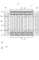
- FIG. 2 is an enlarged view of region II in FIG. 1 and shows a part of a specific example of an IDT electrode;
- FIG. 10 is a diagram showing another specific example (second example) of an IDT electrode;
- FIG. 10 is a diagram showing still another specific example (third example) of an IDT electrode;
- FIG. 10 is a diagram showing still another specific example (fourth example) of an IDT electrode;
- FIG. 10 is a diagram showing still another specific example (fifth example) of the IDT electrode;
- FIG. 10 is a diagram showing still another specific example (sixth example) of an IDT electrode;
- FIG. 10 is a diagram showing still another specific example (seventh example) of the IDT electrode;
- FIG. 10 is a diagram showing another specific example (seventh example) of the IDT electrode;
- FIG. 10 is a diagram showing another specific example (second example) of an IDT electrode;
- FIG. 10 is a diagram showing another specific example (second example) of an IDT electrode;
- FIG. 10 is a diagram showing still another specific example (eighth example) of an IDT electrode;
- FIG. 10 is a diagram showing still another specific example (ninth example) of the IDT electrode;
- FIG. 10 is a diagram showing still another specific example (tenth example) of the IDT electrode;
- FIG. 10 is a diagram showing still another specific example (eleventh example) of an IDT electrode;
- FIG. 2 is a diagram showing an example of a cross section taken along line VI-VI of FIG. 1;
- 2 is a diagram showing another example of a cross section taken along the line VI-VI of FIG. 1;
- FIG. 1 is a plan view showing the configuration of an elastic wave resonator according to an embodiment;
- FIG. 1 is a circuit diagram schematically showing the configuration of a branching filter according to an embodiment
- FIG. 1 is a block diagram showing the configuration of a communication device according to an embodiment
- FIG. FIG. 5 is a diagram showing characteristics of resonators according to the first comparative example and the first example
- FIG. 5 is a diagram showing characteristics of resonators according to first to third examples
- FIG. 10 is a diagram showing characteristics of resonators according to second and third comparative examples and a fourth example;
- any direction of the elastic wave device according to the present disclosure may be upward or downward.
- an orthogonal coordinate system consisting of the D1 axis, the D2 axis and the D3 axis is defined, and terms such as the upper surface and the lower surface may be used with the positive side of the D3 axis being the upper side.
- the term "planar view” or “planar see-through” refers to viewing in the D3 direction.
- the D1 axis is defined to be parallel to the propagation direction of an elastic wave propagating along the upper surface of the piezoelectric body, which will be described later, and the D2 axis is defined to be parallel to the upper surface of the piezoelectric body and perpendicular to the D1 axis. and the D3 axis is defined to be orthogonal to the top surface of the piezoelectric.
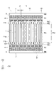
- FIG. 1 is a plan view showing a configuration of a main part of an elastic wave device 1 (hereinafter sometimes simply referred to as "device 1") according to an embodiment.
- the device 1 has, for example, a piezoelectric body 3 (see FIG. 6 and the like, which will be described later), and an IDT electrode 5 located on the upper surface 3a (an example of the first surface) of the piezoelectric body 3.
- FIG. 1 is a plan view of the upper surface 3a. However, the reference numerals relating to the piezoelectric body 3 and the outer edge of the upper surface 3a are omitted from the illustration.
- the device 1 may, for example, constitute resonators and/or filters that utilize such conversion between acoustic waves and voltages (electrical signals).
- the D1 direction may be referred to as an elastic wave propagation direction or a propagation direction.
- the IDT electrode 5 is composed of a conductor layer overlapping the upper surface 3 a of the piezoelectric body 3 . Also, the IDT electrode 5 includes a pair of comb electrodes 7 . Each comb-teeth electrode 7 includes, for example, a busbar 9 and a plurality of electrode fingers 11 electrically connected to the busbar 9 . A pair of comb-teeth electrodes 7 are arranged such that a plurality of electrode fingers 11 mesh with each other (intersect each other).
- the intersection region R0 is a region in which the plurality of electrode fingers 11 of one comb-shaped electrode 7 and the plurality of electrode fingers 11 of the other comb-shaped electrode 7 overlap in the elastic wave propagation direction.
- each comb-teeth electrode 7 has an intervening electrode 41 interposed between the busbar 9 and the plurality of electrode fingers 11 .
- transverse mode spurious can be reduced, as will be described in detail later.
- the configuration other than the configuration related to the intervening electrode 41 may be in various modes, for example, it may be in a known mode. A description of such a configuration that may be a known aspect will be omitted as appropriate.
- the bus bar 9 is formed, for example, in an elongated shape having a substantially constant width and linearly extending in the elastic wave propagation direction (D1 direction).
- the pair of busbars 9 face each other in a direction (D2 direction) perpendicular to the elastic wave propagation direction.
- the edge of each busbar 9 on the side of the intersection region R0 is, for example, linear.
- the edges on the intersection region R0 side are, for example, parallel to each other (the concept of "parallel” may be extended to "curve”). From another point of view, the distance between both edges (D2 direction) is constant regardless of the position in the D1 direction.
- the busbar 9 may vary in width or may be inclined with respect to the propagation direction of the elastic wave. Further, in each bus bar 9, the edge portion on the intersection region R0 side may be curved, or may be formed by a plurality of straight lines that intersect with each other. Also, in the pair of busbars 9, the distance between the edges facing each other may vary depending on the position in the D1 direction.
- the length (D1 direction) of the bus bar 9 may be approximately equal to the product of the pitch p and the number of the plurality of electrode fingers 11 in the pair of comb-teeth electrodes 7, for example.
- the width (D2 direction) of the bus bar 9 is arbitrary. In general, the width of bus bar 9 is greater than the width of electrode fingers 11 (D1 direction). For example, the width of the busbar 9 may be 1p or more.
- the plurality of electrode fingers 11 have, for example, the same shape and dimensions. Unlike the illustrated example, the plurality of electrode fingers 11 may have different shapes and/or sizes. For example, the multiple electrode fingers 11 may have different lengths. That is, the IDT electrode 5 may be a so-called apodized one.
- Each electrode finger 11 is, for example, generally elongated with its center line extending linearly in a direction (D2 direction) orthogonal to the propagation direction of the elastic wave.
- the electrode finger 11 may extend with a constant width (length in the D1 direction), or may vary in width depending on the position in the length direction (D2 direction) (example shown).
- the electrode finger 11 has widened portions 11b at the tip and base sides, the width of which is wider than that of the other major portion (main portion 11a).
- a so-called piston mode (or a mode similar thereto; the same shall apply hereinafter) is utilized, thereby reducing lateral mode spurious. Note that the description of the present embodiment may be expressed on the premise of this aspect.
- each comb-teeth electrode 7 a plurality of electrode fingers 11 are arranged in the acoustic wave propagation direction.
- a line (not shown) connecting the tips (or roots) of the plurality of electrode fingers 11 is, for example, a straight line parallel to the propagation direction.
- the line may be inclined in the propagation direction, curved, or formed of a plurality of straight lines that intersect each other.
- the line may be a straight line parallel to or inclined with respect to the propagation direction.
- the plurality of electrode fingers 11 of one comb-teeth electrode 7 and the electrode fingers 11 of the other comb-teeth electrode 7 are alternately arranged in the propagation direction of the elastic wave.
- the plurality of electrode fingers 11 of one comb-teeth electrode 7 and the electrode fingers 11 of the other comb-teeth electrode 7 may be alternately arranged one by one.
- two or more lines may be alternately arranged.
- a specific portion may exist due to so-called thinning or the like. In the description of the embodiment, an example is taken in which the wires are arranged alternately one by one.
- the pitch p (for example, the center-to-center distance between two adjacent electrode fingers 11) of a pair of comb-teeth electrodes 7 is basically constant within the IDT electrode 5 .
- the IDT electrode 5 may partially have a unique portion with respect to the pitch p.
- the peculiar portions include, for example, a narrow pitch portion in which the pitch p is narrower than the majority (e.g., 80% or more), a wide pitch portion in which the pitch p is wider than the majority, and a portion in which a small number of electrode fingers 11 are substantially spaced.
- a thinning portion that has been drawn can be mentioned.
- the pitch p means the pitch of the portion (most of the plurality of electrode fingers 11) excluding the peculiar portion as described above.
- the average value of the pitches of most of the plurality of electrode fingers 11 is taken as the value of the pitch p. may be used.
- the number of electrode fingers 11 may be appropriately set according to the electrical characteristics required for the IDT electrode 5 (device 1). Since FIG. 1 is a schematic diagram, the number of electrode fingers 11 is shown to be small. Actually, more electrode fingers 11 than illustrated may be arranged. For example, the number of electrode fingers 11 may be 100 or more. Note that FIG. 1 may be understood as a diagram showing an extracted portion of the IDT electrode 5 .
- each electrode finger 11 of one comb-teeth electrode 7 is separated from the edge of the intervening electrode 41 of the other comb-teeth electrode 7 (more specifically, the bar electrode 43 closest to the electrode finger 11 (described later)) and the gap G1. facing through.
- the lengths in the D2 direction of the plurality of gaps G1 are, for example, the same.
- the length may be set as appropriate, and may be, for example, 0.1 p or more and 0.5 p or less.
- the pitch p is set to a half wavelength, and elastic waves propagating in the D1 direction are most likely to be excited.
- the voltage applied to the IDT electrode 5 mainly the component having a frequency equivalent to the frequency of the elastic wave whose half wavelength is approximately the pitch p is converted into an elastic wave.
- the pitch p is set to approximately half the wavelength and the elastic wave propagates in the D1 direction mainly by the principle opposite to the above. Waves are converted into voltage.
- a resonator or filter is realized using such a principle.
- the acoustic wave may be a surface acoustic wave (SAW).
- SAW surface acoustic wave
- the elastic wave may be a plate wave that propagates through a thin plate-like piezoelectric body.
- the Lamb wave for example, an A1 mode Lamb wave, an S0 mode Lamb wave, and an SH (Shear Horizontal) type Lamb wave may be used.
- the elastic wave modes may not be so clearly identifiable or distinguishable.
- the pitch p of the electrode fingers 11 is, as described above, basically half the wavelength of the elastic wave having a frequency equivalent to the intended resonance frequency.
- An example of the absolute value of the pitch p is 0.5 ⁇ m or more and 15 ⁇ m or less.
- the length (D2 direction) of the electrode finger 11 may be, for example, 10p or more or 20p or more, and may be 100p or less or 50p or less. The above lower and upper limits may be combined in any way.
- the duty ratio may be set appropriately.
- the duty ratio of the main portion 11a (or the electrode fingers 11 having a constant width over the entire length) may be 0.40 or more or 0.45 or more, or 0.60 or less or 0.55 or less. may be assumed.
- the above upper and lower limits may be combined in any way.
- the duty ratio of the widened portion 11b may be 0.50 or more or 0.55 or more, provided that it is larger than the duty ratio of the main portion 11a. or less or 0.65 or less.
- the above upper and lower limits may be combined in any way.
- each electrode finger 11 has one main portion 11a and two widened portions 11b
- these lengths may be set as appropriate.
- the length of one widened portion 11b may be 0.5p or more, 0.7p or more, or 0.9p or more, or may be 2p or less, 1.5p or less, or 1.1p or less.
- the above upper and lower limits may be combined in any way.
- the thickness of the IDT electrode 5 is, for example, generally constant regardless of the position in the planar direction (direction parallel to the D1-D2 plane).
- the thickness of the conductor layer may be appropriately set according to the properties required of the device 1 .
- the thickness of the conductor layer may be between 0.04p and 0.20p and/or between 50nm and 600nm.
- the conductor layer is made of metal, for example.
- the metal may be of any suitable type, such as aluminum (Al) or an alloy based on Al (Al alloy).
- the Al alloy is, for example, an Al-copper (Cu) alloy.
- the conductor layer may be composed of multiple metal layers.
- the conductor layer may be composed of a relatively thin layer of titanium (Ti) overlaid on the upper surface 3a of the piezoelectric body 3 and Al or an Al alloy overlaid thereon. Ti contributes, for example, to strengthening the bondability between Al or an Al alloy and the piezoelectric body 3 .
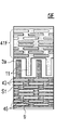
- FIG. 2 is an enlarged view of area II of FIG.
- FIG. 2 illustrates an intervening electrode 41A according to the first example.
- the busbar 9, the electrode fingers 11 and the intervening electrodes 41 are connected to each other unless otherwise noted or contradictory. 1 (within one comb-teeth electrode 7).
- the intervening electrode 41 is, for example, generally configured in a lattice or mesh. Specifically, for example, the intervening electrode 41 has two types of parts: a plurality of (eight in the illustrated example) bar electrodes 43 and a plurality of connecting portions 45 .
- the plurality of bar electrodes 43 extend parallel to the busbar 9 and extend parallel to each other.
- a region between two adjacent bar electrodes 43 (or adjacent bar electrodes 43 and busbars 9) may be referred to as a slit region S1.
- Each connecting portion 45 is positioned in the slit region S1 and connects two adjacent bar electrodes 43 (or adjacent bar electrodes 43 and bus bars 9).
- At least some (all in the illustrated example) of the plurality of connecting portions 45 are arranged discontinuously with respect to the extending direction (D2 direction) of the electrode fingers 11 . That is, at least some of the plurality of connecting portions 45 are not arranged to form a straight line parallel to the direction D2 extending from the bus bar 9 to the bar electrode 43 closest to the electrode finger 11 side. From another point of view, at least a part of at least one connecting portion 45 has no conductor (IDT electrode 5) in at least one slit region S1 (for example, adjacent slit region S1) other than the slit region S1 in which it is located. It overlaps with the area in the D2 direction.
- spurious can be reduced.
- the applicant has confirmed this effect through actual measurements and simulation calculations in a prototype, and will show some examples later.
- Principles that can reduce spurious include the following.
- the elastic wave is reflected at the boundary between the area where the conductor (IDT electrode 5) is arranged and the area where the conductor (IDT electrode 5) is not arranged. If all the connecting portions 45 are arranged to form a straight line parallel to the direction D2, the transverse mode spurious is generated at the position of the straight line in the direction D1 by the bar electrode 43 closest to the electrode finger 11. , and is reflected by each of the plurality of bar electrodes 43 (and bus bars 9) at other positions in the D1 direction. That is, the position in the D2 direction where reflection occurs is basically constant regardless of the position in the D1 direction. As a result, transverse mode spurs tend to align in wavelength and node and antinode positions, and thus tend to reinforce each other.
- connection portions 45 are arranged discontinuously in the D2 direction as in the present embodiment, a conductor non-arrangement region exists at a position overlapping the connection portions 45 in the D2 direction.
- Transverse mode spurious signals are also reflected between the non-arrangement area and the bar electrode 43 . Reflection also occurs at the connection portion 45 depending on the shape of the connection portion 45 . The positions of these new reflections are distributed in positions in the D1 and D2 directions. As a result, the transverse mode spurs are dispersed in wavelength and node and antinode locations, thus reducing their mutually constructive effects.
- connection portions 45 are arranged discontinuously in the D2 direction, the number, shape, position, size, etc. of the plurality of bar electrodes 43 and the plurality of connection portions 45 are Optional.
- the number, shape, position, size, etc. of the plurality of bar electrodes 43 and the plurality of connection portions 45 are Optional.
- the number, shape, position, size, etc. of the plurality of bar electrodes 43 and the plurality of connection portions 45 are Optional.
- the number of the plurality of bar electrodes 43 may be any number of 2 or more.
- two slit regions S1 are formed by the two bar electrodes 43 and the busbars 9 .
- at least two connecting portions 45 located in mutually different slit regions S1 can be arranged discontinuously in the D2 direction.
- the plurality of bar electrodes 43 have, for example, the same shape and dimensions as each other. Moreover, each bar electrode 43 has a shape extending linearly with a substantially constant width. From another point of view, the shape of the edge or the center line of the bar electrode 43 is the same as the shape of the edge of the bus bar 9 on the side of the electrode fingers 11 and/or the electrodes facing the intervening electrode 41 via the gap G1. It has the same shape as the line connecting the tips of the fingers 11 (the tips of the electrode fingers 11 of the comb-teeth electrode 7 meshing with the comb-teeth electrode 7 to which the bar electrode 43 of interest belongs).
- At least one bar electrode 43 has a different shape and/or size with respect to at least one other bar electrode 43 .
- may have The width (D2 direction) of the bar electrode 43 may vary depending on the position in the D1 direction.
- the centerline and/or edge of the bar electrode 43 may be curved or may have a plurality of straight lines that intersect each other. Further, the shape of the center line and/or the edge of the bar electrode 43 may be different from the shape of the edge of the bus bar 9 on the side of the electrode fingers 11, and/or the shape of the edge of the bus bar 9 may be different from that of the electrode finger 11 side, It may be different from the shape of the line connecting the tips of the electrode fingers 11 .
- the length of the bar electrode 43 may be approximately equal to the length of the busbar 9 .
- the width of the bar electrode 43 may be, for example, smaller than the width of the bus bar 9 (D2 direction) and/or the width of the electrode fingers 11 (D1 direction) (example shown), equal to or larger than the width of the bus bar 9 (D2 direction).
- the width of the bar electrode 43 may be 0.1p or more or 0.2p or more, and may be 0.5p or less or 0.3p or less. The above lower and upper limits may be combined in any way.
- the plurality of bar electrodes 43 extend parallel to the busbar 9 and extend parallel to each other. More specifically, in the illustrated example, the plurality of bar electrodes 43 (for example, center lines; hereinafter the same) and the edges of the bus bars 9 on the side of the electrode fingers 11 extend parallel to each other. From another point of view, the distance in the D2 direction (extending direction of the electrode fingers 11) is constant regardless of the position in the D1 direction (propagation direction of the elastic wave). The direction in which the plurality of bar electrodes 43 (and the busbars 9) extend is, for example, the D1 direction.
- part or all of at least one bar electrode 43 may be inclined with respect to the busbar 9, at least one other bar electrode 43, and/or the D1 direction.
- the bar electrodes 43 may have portions that intersect the busbars 9 and/or other bar electrodes 43 .
- a part of the intersecting portion may be regarded as a type of connection portion 45, and the plurality of bar electrodes 43 may be regarded as not intersecting.
- the pitches of the plurality of bar electrodes 43 are, for example, the same. However, at least one pitch may differ from the other pitches. Also, the pitch of the bar electrodes 43 may be smaller than the pitch p of the electrode fingers 11 (example shown), equal to it, or larger. The pitch of the bar electrodes 43 may be, for example, 0.2p or more or 0.4p or more, and may be 1p or less or 0.6p or less. The above lower and upper limits may be combined in any way.
- the widths (D2 direction) of the plurality of slit regions S1 are, for example, the same. However, at least one width may differ from the other widths. Also, the width of the slit region S1 may be smaller than the pitch p of the electrode fingers 11 (example shown in the figure), equal to it, or larger. For example, the width of the slit region S1 may be 0.1p or more or 0.2p or more, and may be 0.5p or less or 0.3p or less. The above lower and upper limits may be combined in any way.
- the ratio of the width of the bar electrodes 43 to the pitch of the bar electrodes 43 may be smaller or equal to the duty ratio of the electrode fingers 11, for example. It can be big.
- the duty ratio of the bar electrode 43 may be 0.1 or more or 0.4 or more, and may be 0.8 or less or 0.6 or less. The above lower and upper limits may be combined in any way.
- the shapes and dimensions of the plurality of connecting portions 45 are, for example, identical to each other.
- the discontinuity of the plurality of connection portions 45 with respect to the D2 direction is such that the positions of the plurality of connection portions 45 (for example, the position of the geometric center; unless otherwise specified, the same applies hereinafter) are on a straight line parallel to the D2 direction. It is realized by not being located (displaced from each other in direction D1). However, unlike the illustrated example, the shapes and dimensions of the plurality of connecting portions 45 may be different from each other. In this case, discontinuity in the D2 direction may be realized by the difference in shape and/or size of the plurality of connecting portions 45 in addition to or instead of the positional deviation in the D1 direction.
- connection portion 45 for example, a rectangular shape having four sides parallel to the D1 direction and the D2 direction (see FIG. 4A), or a parallelogram shape having two sides parallel to the D1 direction (example of FIG. 2), or these (see, for example, FIG. 5).
- the length of the connection portion 45 in the D2 direction is the same as the width of the slit region S1, and the width is as described above.
- the length of the connection portion 45 in the D1 direction may be set appropriately.
- the length of the connecting portion 45 in the D1 direction may be shorter than, equal to, or longer than the length of the connecting portion 45 in the D2 direction.
- the length of the connection portion 45 in the D1 direction may be 0.1p or more, 0.3p or more, or 0.5p or more, and may be 1p or less, 0.8p or less, or 0.7p or less. you can The above lower and upper limits may be combined in any way.
- 3A to 5 are plan views showing other specific examples of the IDT electrode 5 (especially the intervening electrode 41).
- 3A to 3D and FIG. 5, like FIG. 2 show the range corresponding to area II in FIG. 4A to 4E show a partial range of a pair of comb electrodes 7 in the D1 direction.
- the orthogonal coordinate system D1-D2-D3 is omitted, but as in FIG. 2, the horizontal direction in the drawing is the D1 direction, and the vertical direction in the drawing is the D2 direction. is.
- the plurality of connecting portions 45 are arranged to form a straight line inclined in the D2 direction.
- the straight line extends, for example, from the bus bar 9 to the bar electrode 43 closest to the electrode finger 11 side. Focusing on two adjacent straight lines in the D1 direction, the plurality of connecting portions 45 are arranged in a V shape that closes (or opens) toward the electrode finger 11 side.
- a plurality of V-shapes are arranged so as to connect with each other in the D1 direction.
- the plurality of connecting portions 45 are arranged in a zigzag line extending in the D1 direction. Note that, unlike the illustrated example, one V-shape may be positioned at a specific position in the D1 direction, or adjacent V-shapes may be separated from each other.
- a closed V is formed.
- the electrode finger it may be understood that a closed V shape is formed on the 11 side. The same applies to the case where a closed V shape is formed on the busbar 9 side.
- connection portion 45 positioned closest to the electrode finger 11 and the connection portion positioned closest to the busbar 9 The position of 45 in the D1 direction may be set appropriately.
- the connection portion 45 positioned closest to the electrode finger 11 may be positioned at the position in the D1 direction of the electrode finger 11 of the comb-teeth electrode 7 to which it belongs (see the center side in the left-right direction of FIG. 3A).
- the inclination angle of the straight line may be set as appropriate.
- the size of the V shape in the D1 direction may be set appropriately.
- the distance (relative position) in the D1 direction between the connecting portion 45 positioned closest to the electrode finger 11 and the connecting portion 45 positioned closest to the busbar 9 on the straight line may be appropriately set.
- the pitch of the plurality of V-shaped arrangements may be set as appropriate.
- a linear or V-shaped arrangement range in the D1 direction is considered (in another specific example, a straight line or a V-shaped
- the arrangement range of one straight line in the D1 direction may be 0.1p or more or 0.2p or more, and may be 2.0p or less, 1.5p or less, or 1.2p or less.
- the above lower and upper limits may be combined in any way.
- the arrangement range of one straight line in the D1 direction is approximately 1p (for example, 0.8p or more and 1.2p or less).
- the arrangement range of the V shape in the D1 direction is approximately 2p (for example, 1.8p or more and 2.2p or less).
- the edge on the -D1 side or +D1 side of the plurality of connecting portions 45 arranged linearly (or curvedly). At this time, the edge is located on the same straight line (or on the same curve) that is inclined in the D1 direction (not stepped like in FIG. 4C). In other words, the ⁇ D1 side edges and/or the +D side edges of the plurality of connection portions 45 are configured as if they are smoothly connected to each other (strictly speaking, the bar electrodes 43 are interposed). there is.). In any aspect in which the plurality of connection portions 45 are arranged in a V shape or other shape, the edge on the -D1 side and/or the edge on the +D side are configured as if they were smoothly connected. It may or may not.
- adjacent connecting portions 45 may partially overlap in the D2 direction (example in FIG. 2) or may not overlap. (see FIGS. 4A and 4E).
- the amount of overlap in the former case is arbitrary, and may be smaller, equal, or larger than half the length of one connecting portion 45 in the D1 direction, for example.
- the distance between the two connections 45 in the latter case is arbitrary, for example the distance may be 0 (examples of FIGS. 4A and 4E) or greater than 0.
- the intervening electrode 41B (IDT electrode 5B) shown in FIG. 3A has a plurality of connecting portions 45 arranged in a V-shape like the intervening electrode 41A in FIG.
- the size of the V shape in the D1 direction is made smaller than that in the intervening electrode 41A.
- the number of V-shaped repeats arranged in a predetermined length range in the D1 direction is large.
- the arrangement range of one straight line in the D1 direction is approximately 0.5p (for example, 0.3p or more and 0.7p or less).
- the arrangement range of the V shape in the D1 direction is approximately 1p (for example, 0.8p or more and 1.2p or less).
- connection portions 45 are arranged in a Y shape opening toward the electrode finger 11 side.
- the plurality of connecting portions 45 may include two or more connecting portions 45 arranged in a straight line parallel to the D2 direction.
- a plurality of connection portions 45 (the number of which is smaller than the number of the slit regions S1) positioned on the electrode finger 11 side are arranged in a V shape that opens toward the electrode finger 11 side. .
- the description of the V-shape of the intervening electrode 41A may be appropriately incorporated into the V-shape of the Y-shape of the intervening electrode 41C.
- the ratio between the number of slit regions S1 forming the V-shaped portion of the Y-shape and the number of slit regions S1 forming the I-shaped portion of the Y-shape is arbitrary.
- a plurality of electrode fingers 11 extend over the entire length with a constant width.
- the intervening electrode 41A of FIG. 2 is illustrated as the intervening electrode 41.
- the electrode fingers 11 extending with a constant width over the entire length may be combined with other specific examples of the intervening electrodes 41 .
- electrode fingers 11 having widened portions 11b may be combined with any specific example of intervening electrode 41 .
- the IDT electrode 5E shown in FIG. 3D has a so-called dummy electrode 25.
- the plurality of dummy electrodes 25 extend in parallel with the plurality of electrode fingers 11 from the intervening electrode 41 (more specifically, the bar electrode 43 closest to the electrode fingers 11 ).
- the tips of the dummy electrodes 25 of one comb-teeth electrode 7 face the tips of the electrode fingers 11 of the other comb-teeth electrode 7 with a gap G1 interposed therebetween.
- the shape of the dummy electrode 25 may be set appropriately.
- the shape of the dummy electrode 25 is generally a shape protruding in a direction perpendicular to the propagation direction of the elastic wave with a constant width.
- the width of the dummy electrode 25 is the same as the width of the electrode finger 11 without the widened portion 11b (or the width of the main portion 11a of the electrode finger 11 with the widened portion 11b).
- the width of the dummy electrode 25 may be partially widened on the gap G1 side and/or the bus bar 9 side.
- the presence or absence of the widened portions of the electrode fingers 11 and the dummy electrodes 25 can be combined arbitrarily.
- a combination of electrode fingers 11 having a widened portion and dummy electrodes 25 not having a widened portion, a combination of electrode fingers 11 having a widened portion and dummy electrodes 25 having a widened portion, and a widened portion A combination of the electrode fingers 11 having no width and the dummy electrode 25 having the widened portion may be employed.
- the width of the dummy electrodes 25 may be, for example, equal to the width of the main portion 11a, or the widened portion 11b. may be equal to the width of
- the intervening electrode 41A of FIG. 2 is illustrated as the intervening electrode 41.
- the dummy electrode 25 may be combined with other specific examples of the intervening electrode 41 .
- the embodiment without dummy electrode 25 may be applied to any specific example of intervening electrode 41 .
- a plurality of connecting portions 45 are arranged in a straight line inclined in the D2 direction, similar to the intervening electrode 41A in FIG.
- the plurality of connecting portions 45 are arranged in a V shape that opens to one side in the D1 direction (the right side in FIG. 4A), not in a V shape that opens to the electrode finger 11 side.
- the plurality of connection portions 45 are arranged along two straight lines that incline opposite to each other with respect to the D2 direction and intersect each other.
- the direction in which the V-shape opens may be the same (example shown) or different between the pair of comb-tooth electrodes 7 .
- the plurality of connecting portions 45 may be arranged along three or more straight lines (zigzag paths) that intersect in order. Although two connecting portions 45 are positioned at the intersection of the straight lines, only one connecting portion 45 may be positioned.
- the lengths and/or angles of inclination of the two (or more) straight lines formed by the plurality of connection portions 45 may be the same (example shown) or may be different.
- the edges on the -D1 side or +D1 side of the plurality of linearly arranged connecting portions 45 may be positioned on the same straight line (smoothly connected). ) or may not be located. In the example of FIG. 4A, the latter is adopted, and the edges of the plurality of connecting portions 45 are stepped.
- the connecting portions 45 adjacent to each other may or may not partially overlap each other in the D2 direction. may In the example of FIG. 4A, it is the latter, and more specifically, the connecting portions 45 adjacent to each other are adjacent to each other when projected in the D1 direction (the distance between them is 0).
- the plurality of connecting portions 45 are arranged in a checkered pattern. From another point of view, the plurality of connecting portions 45 are arranged in a plurality of mutually parallel straight lines inclined in the D2 direction, and the plurality of straight lines partially overlap each other in the D2 direction.
- the plurality of connection portions 45 are arranged in a plurality of mutually parallel straight lines that are inclined with respect to the D2 direction.
- the plurality of straight lines have different arrangement ranges in the D1 direction and do not overlap each other in the D2 direction.
- the intervening electrode 41I (IDT electrode 5I) shown in FIG. 4D has substantially the same configuration as the intervening electrode 41H in FIG. 4C. That is, the plurality of connecting portions 45 are arranged in a plurality of parallel straight lines that are inclined with respect to the D2 direction (extending direction of the electrode fingers 11). However, in FIG. 4C, the straight line of one comb-teeth electrode 7 and the straight line of the other comb-teeth electrode 7 are inclined opposite to each other with respect to the D2 direction, whereas in FIG. The straight line of the electrode 7 and the straight line of the other comb-teeth electrode 7 are inclined to the same side.
- the intervening electrode 41J (IDT electrode 5J) shown in FIG. 4E has substantially the same configuration as the intervening electrode 41H in FIG. 4C. That is, the plurality of connecting portions 45 are arranged in a plurality of parallel straight lines that are inclined with respect to the D2 direction (extending direction of the electrode fingers 11). However, unlike the intervening electrode 41H, the plurality of straight lines of the intervening electrode 41J partially overlap each other in the D2 direction by an amount that does not result in a checkerboard pattern (see the intervening electrode 41G in FIG. 4B).
- IDT electrode 41K In the intervening electrode 41K (IDT electrode 5K) shown in FIG. 5, a region (a conductor-free region) surrounded by the connecting portions 45 adjacent to each other in each slit region S1 and the bar electrodes 43 on both sides of each slit region S1. shall be referred to as an aperture region 47. At least one (all in the illustrated example) of the plurality of opening regions 47 has an elliptical shape. Note that the ellipse referred to here does not have to be an ellipse defined by mathematics. For example, if the edge portions on both sides in the D1 direction are curvilinear and bulging outward, it may be regarded as an elliptical shape.
- an ellipse is, for example, a shape obtained by squashing a circle in the D2 direction.
- a circle may also be included in an ellipse.
- the elliptical shape referred to here may also include a shape in which the short sides of a rectangle are curved outward.
- an example is taken in which a plurality of connecting portions 45 are arranged in a V shape.
- the elliptical opening region 47 may be applied to other aspects.
- the plurality of connecting portions 45 may be arranged in an X shape.
- multiple connections 45 may be arranged along a curve.
- the area where the IDT electrodes 5 are arranged can be divided into the following four areas in the D2 direction based on the configuration of the IDT electrodes 5 .
- Gap region RG where gap G1 is located.
- an intervening region RI where the intervening electrode 41 is located;
- the intersection region R0 is a region sandwiched between a line (not shown) connecting the tips of the electrode fingers 11 of one comb-teeth electrode 7 and a line (not shown) connecting the tips of the electrode fingers 11 of the other comb-teeth electrode 7.
- a line connecting predetermined portions (for example, tips) of the plurality of electrode fingers 11 if the position of the line differs depending on which position within the width of the electrode finger 11 is used as a reference, The center line of the electrode finger 11 may be used as a reference.
- the intersection region R0 can be divided into the following two (three) regions in the D2 direction based on the width of the electrode fingers 11.
- a central region RC in which a plurality of main portions 11a overlap each other in the D1 direction.
- An edge region RE in which a plurality of widened portions 11b overlap each other in the D2 direction.
- D2 direction refer to the description of the main portion 11a and the widened portion 11b.
- the speed of sound referred to here may be, for example, the speed at which the elastic wave of the mode utilized by the device 1 propagates through the piezoelectric body 3 .
- the speed of sound referred to here may be, for example, the speed at which the elastic wave of the mode utilized by the device 1 propagates through the piezoelectric body 3 .
- the relationship between the speeds of sound in the plurality of regions is reversed according to the difference in the specific mode of the elastic wave used. never. Therefore, when considering the relationship between high and low sound velocities to be described below, it is not necessary to specify which mode the sound velocity of the elastic wave is.
- the sound velocity of the elastic wave is affected by the mass of the member (for example, the IDT electrode 5) located on the upper surface 3a of the piezoelectric body 3. For example, in each region, the greater the mass per unit area, the lower the speed of sound. On the other hand, when the thickness of the conductor layer forming the IDT electrode 5 is constant, the mass per unit area increases as the ratio of the conductor layer to the unit area increases. Therefore, the greater the area ratio of the conductor layer forming the IDT electrode 5, the lower the sound velocity.
- the areas with the lowest sound velocities are named, for example, the busbar area RB, the intersection area R0, and the gap area RG.
- the sound velocity in the edge region RE is lower than that in the central region RC.
- the speed of sound in the intervening region RI is higher than the speed of sound in the busbar region RB.
- the speed of sound in the intervening region RI may be lower than, equal to, or higher than the speed of sound in the intersecting region R0 and the gap region RG.
- the sound velocity of the intervening region RI is lower than the sound speed of the gap region RG and the sound speed of the central region RC (or the intersecting region R0 where the width of the electrode fingers 11 is constant over the entire length).
- the speed of sound in the intersection region R0 may change in three or more steps instead of two steps.
- the central region RC may include two or more regions with different sound velocities. The same is true for the edge region RE.
- the change in the speed of sound with respect to the position in the D2 direction may not be stepwise but may be continuous.
- the speed profile (relationship between high and low speeds between regions) described above may be realized by a method other than the ratio of the conductor layer to the unit area. For example, by providing an additional film (described later) that partially overlaps the upper or lower surface of the IDT electrode 5, the velocity in the region provided with the additional film may be reduced.
- the speed of the thickened region may be reduced.
- the insulating film may be provided at an appropriate position, thereby reducing the speed of the area provided with the insulating film.
- the piezoelectric body 3 having the upper surface 3a on which the IDT electrodes 5 are formed may be, for example, part or all of the substrate.
- the configuration of the substrate may be in various modes, for example, it may be in a known mode.
- the configuration of the substrate is exemplified below.
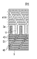
- FIG. 6 is a cross-sectional view showing the configuration of a substrate 13A as a first example of the substrate.
- the illustrated cross section corresponds to the cross section taken along line VI-VI in FIG.
- the substrate 13A has, for example, a supporting substrate 15, an intermediate layer 17 overlapping the upper surface of the supporting substrate 15, and a piezoelectric body 3 overlapping the upper surface of the intermediate layer 17.
- the piezoelectric body 3 is constructed as a piezoelectric film.
- the terms "plate”, “layer” and “film” are the same unless otherwise specified.
- the thickness of each layer is, for example, constant regardless of the position in the planar direction (direction parallel to the D1-D2 plane).
- the piezoelectric body 3 is made of, for example, a piezoelectric single crystal.
- materials constituting such a single crystal include lithium tantalate (LiTaO 3 , hereinafter sometimes abbreviated as LT), lithium niobate (LiNbO 3 , hereinafter sometimes abbreviated as LN), and Quartz (SiO 2 ) may be mentioned.
- the piezoelectric body 3 may be made of polycrystal. The cut angle, planar shape and various dimensions of the piezoelectric body 3 may be appropriately set.
- a piezoelectric body of LT or LN may be of rotational Y-cut X-propagation.
- the elastic wave propagation direction (D1 direction) and the X axis may substantially coincide (for example, the difference between the two is ⁇ 10°).
- the inclination angle of the Y-axis with respect to the normal line (D3 direction) of the upper surface 3a of the piezoelectric body 3 may be set appropriately.
- the thickness of the piezoelectric body 3 may be, for example, 0.1p or more or 0.3p or more, and may be 2p or less or 1p or less. The above upper limit and lower limit may be combined appropriately.
- the supporting substrate 15 may contribute to at least one of, for example, improving the strength of the substrate 13A, compensating for characteristic changes due to temperature changes (temperature compensation), and confining elastic waves in the piezoelectric body 3.
- An improvement in strength may be realized, for example, by appropriately setting the thickness of the support substrate 15 made of a material having a certain degree of strength.
- Temperature compensation may be realized, for example, by making the coefficient of linear expansion of the support substrate 15 smaller than the coefficient of linear expansion of the piezoelectric body 3 .
- Acoustic waves are confined by, for example, the support substrate 15 having a higher sound velocity than the piezoelectric body 3 (and/or the intermediate layer 17), and/or the acoustic impedance of the support substrate 15 and the acoustic impedance of the intermediate layer 17 It may be realized by different things.
- the material and thickness of the support substrate 15 may be appropriately set in light of the above purposes.
- the material of the support substrate 15 may be a semiconductor such as silicon (Si), a single crystal such as sapphire (Al 2 O 3 ), or a ceramic such as sintered aluminum oxide (Al 2 O 3 ).
- the thickness of the support substrate 15 is, for example, 1p or more or 3p or more.
- the thickness of the support substrate 15 is thicker than the thickness of the piezoelectric body 3, for example.
- the intermediate layer 17 may contribute, for example, to at least one of improving the bonding strength between the piezoelectric body 3 and the support substrate 15 and confining the elastic wave to the piezoelectric body 3 . Improving the bonding strength may be achieved by selecting, as the material of the intermediate layer 17, a material that has relatively high bonding strength with the piezoelectric body 3 and the support substrate 15 when a predetermined bonding method is used, for example. . Acoustic wave confinement is achieved, for example, by having the acoustic velocity of the intermediate layer 17 lower than that of the piezoelectric body 3 (and/or the support substrate 15), and/or the acoustic impedance of the intermediate layer 17 and the piezoelectric body 3 (and/or the support substrate 15). It may be realized by different acoustic impedance of the substrate 15).
- the material and thickness of the intermediate layer 17 may be appropriately set in light of the above purposes.
- the material of intermediate layer 17 may be silicon oxide (SiO 2 ).
- the thickness of the intermediate layer 17 may be, for example, 0.01p or more, or 0.1p or more, and may be 2p or less, 1p or less, or 0.5p or less. The above upper limit and lower limit may be combined as appropriate.
- the thickness of the intermediate layer 17 is thinner than the thickness of the support substrate 15, for example.
- the thickness of the intermediate layer 17 may be thinner than, equal to, or thicker than the thickness of the piezoelectric body 3 .
- the intermediate layer 17 may be a low sound velocity layer whose sound velocity is lower than that of the piezoelectric body 3
- the support substrate 15 may be a high sound velocity layer whose sound velocity is higher than that of the piezoelectric body 3 .
- the sound velocity referred to here may be, for example, the shear wave sound velocity determined by the physical property values of each material itself. In other words, unlike the sound velocity described in the velocity profile in the region where the IDT electrodes 5 are arranged, the influence of the IDT electrodes 5 can be ignored.
- the shear wave speed is given by the square root of the elastic modulus divided by the density.
- the sound velocity of the piezoelectric body 3 to be compared with the sound velocity of the intermediate layer 17 and the support substrate 15 is the central region RC of the elastic wave of the mode to be used (the width of the electrode finger 11 is In certain aspects, it may be the speed of sound in the intersection region R0).
- the acoustic velocity of the intermediate layer 17 and/or the support substrate 15 may be the acoustic velocity of the bulk wave of the mode that has a relatively large effect on the energy leakage of the elastic wave of the utilized mode.
- the combination of the material of the intermediate layer 17 as the low acoustic velocity layer and the material of the support substrate 15 as the high acoustic velocity layer is arbitrary.
- combinations of these materials can include the combination of SiO 2 and Si described above.
- a layer that improves the bonding strength between the intermediate layer 17 and the piezoelectric body 3 and/or a layer that improves the bonding strength between the intermediate layer 17 and the support substrate 15 A thin layer may be provided.
- FIG. 7 is a cross-sectional view showing the configuration of a substrate 13B as a second example of the substrate.
- the illustrated cross section corresponds to the cross section taken along line VI-VI in FIG.
- the substrate 13B is obtained by providing a multilayer film 19 in place of the intermediate layer 17 in the substrate 13A described above.
- the multilayer film 19 has two or more layers (six layers in the illustrated example) of acoustic films (first film 21A and second film 21B).
- the materials of the multiple layers of acoustic membranes are different between the acoustic membranes adjacent to each other in the lamination direction (overlapping each other without another acoustic membrane interposed). From another point of view, adjacent acoustic membranes have different acoustic impedances.
- the reflectance of elastic waves is relatively high at the interface between the two.
- leakage of elastic waves propagating through the piezoelectric body 3 is reduced.
- the combination of the intermediate layer 17 and the support substrate 15 in the substrate 13A of FIG. 6 may be regarded as a type of multilayer film.
- a multi-layer film may be defined including the support substrate 15.
- the number of types of materials for the acoustic films of the multilayer film 19 and the number of acoustic films may be set as appropriate.
- two types of acoustic films (first film 21A and second film 21B) are alternately laminated in three or more layers (more specifically, six layers).
- the material of the acoustic membrane is also arbitrary.
- the material of the first film 21A may be silicon dioxide (SiO 2 ).
- the material of the second film 21B is tantalum pentoxide (Ta 2 O 5 ), hafnium oxide (HfO 2 ), zirconium dioxide (ZrO 2 ), titanium oxide (TiO 2 ), magnesium oxide (MgO) or silicon nitride (Si 3 N 4 ).
- the first film 21A has, for example, a lower acoustic impedance than the second film 21B.
- the thickness of the acoustic membrane may be set as appropriate, and for example, the above description of the thickness of the intermediate layer 17 may be used.
- the acoustic membranes may constitute the low acoustic velocity membrane and the high acoustic velocity membrane, like the intermediate layer 17 and the support substrate 15 of the substrate 13A of FIG.
- the first film 21A may be made of a material (such as SiO 2 or Ta 2 O 5 ) having a lower sound speed than the piezoelectric body 3 .
- the second film 21B may be made of a material (for example, Si 3 N 4 ) having a higher sound velocity than the piezoelectric body 3 .
- the substrate including the piezoelectric body 3 may be in various forms other than the above examples.
- the substrate may be composed almost entirely of the piezoelectric body 3 .
- the piezoelectric body 3 may be made relatively thick.
- the substrate may have a cavity below the relatively thin (for example, thickness of 2p or less or 1p or less) piezoelectric body 3 .
- the substrate may have a high sound velocity layer that overlaps with the lower surface of the intermediate layer 17 as a low sound velocity layer, separately from the support substrate 15.
- acoustic wave confinement may be achieved by a high acoustic velocity layer overlapping the lower surface of piezoelectric body 3 .
- the acoustic wave device 1 may have an insulating protective film covering the upper surface 3a of the piezoelectric body 3 from above the conductor layer including the IDT electrodes 5 .
- the protective film may, for example, contribute to reducing corrosion of the conductor layer and/or contribute to temperature compensation. Examples of materials for the protective film include SiO 2 , Si 3 N 4 and Si.
- the protective film may be a laminate of these materials.
- the device 1 may have an additional film that overlaps the upper or lower surface of the IDT electrode 5 .
- the additional film for example, overlaps all or part of the IDT electrode 5 and has a shape that fits within the IDT electrode 5 when seen through a plan view.
- Such an additional film is made of, for example, an insulating material or a metal material that has different acoustic properties from the material of the IDT electrode 5, and contributes to improving the reflection coefficient of elastic waves.
- the device 1 may be packaged appropriately.
- Examples of the configuration of the package include the following. A package in which a substrate 13A (or 13B or the like) is mounted on a substrate (not shown) so that the upper surface 3a of the piezoelectric body 3 is opposed to the substrate with a gap therebetween, and the substrate is sealed with mold resin.
- a wafer level package in which a box-shaped cover covering the upper surface 3a is provided on the substrate 13A (or 13B or the like).
- the elastic wave device 1 has the piezoelectric body 3 and the IDT electrodes 5 .
- the piezoelectric body 3 has a first surface (upper surface 3a).
- the IDT electrode 5 is located on the upper surface 3a.
- the IDT electrode 5 has the following parts. First bus bar (bus bar 9 of one comb tooth electrode 7).
- a second bus bar facing the first bus bar (the bus bar 9 of the other comb tooth electrode 7).
- a plurality of first electrode fingers electrode fingers 11 of one comb-teeth electrode 7) electrically connected to the first bus bars respectively.
- a plurality of second electrode fingers (electrode fingers 11 of the other comb-teeth electrode 7) electrically connected to the second bus bars and alternately arranged in the acoustic wave propagation direction (D1 direction) with the plurality of first electrode fingers. ).
- a plurality of bar electrodes 43 interposed between the first bus bars and between the plurality of first electrode fingers, extending parallel to the first bus bars and extending parallel to each other (here, one of the comb-tooth electrodes) 7 bar electrode 43 as an example).
- a connecting portion 45 interposed between and connecting the first bus bar and the bar electrode 43 adjacent to the first bus bar, and a connecting portion interposed between and connecting the adjacent bar electrodes 43. 45 and a plurality (at least two) of connections 45 . At least some of the plurality of connecting portions 45 are arranged discontinuously with respect to the extending direction (D2 direction) of the plurality of electrode fingers 11 .
- the plurality of connecting portions 45 may be arranged in a direction inclined with respect to the extending direction (D2 direction) of the electrode fingers 11 (FIGS. 2 to 5).
- the plurality of connecting portions 45 may be arranged in a V shape that closes toward the side of the plurality of electrode fingers 11 (FIGS. 2 and 3A to 3D).
- the plurality of connecting portions 45 may be arranged in a Y shape that opens toward the side of the plurality of electrode fingers 11 (FIG. 3B).
- the same effect as above can be achieved.
- the size of the V-shape included in the Y-shape can be adjusted in the D2 direction.
- the bar electrodes 43 remaining after the adjustment are maintained at the same potential by the I-shape included in the Y-shape.
- the area where the IDT electrode 5 is located may have the following areas.
- a gap region where a gap G1 adjacent to the intervening region RI side with respect to the tips of a plurality of second electrode fingers (the electrode fingers 11 of the comb-teeth electrode 7 meshing with the comb-teeth electrode 7 to which the intervening electrode 41 of interest belongs) is located RG.
- intersection region R0 may have the following regions.
- a central region RC located in the center of the intersection region R0 in the D2 direction and having a lower sound speed than the gap region RG.
- An edge region RE located between the central region RC and the gap region RG and having a lower sound velocity than the central region RC.
- the intervening region RI may have a higher sound velocity than the busbar region RB.
- the lateral mode spurious is reduced by using the piston mode, so the lateral mode spurious can be further reduced.
- the intervening electrode 41 functions in the same manner as the busbar 9, reducing the significance of providing the intervening electrode 41 between the busbar 9 and the gap region RG. do.
- the effect of dispersing the reflection positions of the transverse mode spurious is reduced.
- such a problem is reduced because the intervening region RI has a higher sound speed than the busbar region RB.
- the edge portions of the plurality of connection portions 45 located on one side (+D1 side or -D1 side) in the elastic wave propagation direction are on the same straight line or the same curved line inclined with respect to the extending direction (D2 direction) of the electrode fingers 11. It may be located above (FIGS. 2-3D).
- the edge of each connection portion 45 can constitute the reflection position of the transverse mode spurious, and The position can be changed in the D2 direction depending on the position in the D1 direction. As a result, the effect of reducing spurious is improved.
- connection parts 45 having different positions in the acoustic wave propagation direction (D1 direction) may be positioned.
- a region (opening region 47) surrounded by the two or more connection portions 45 and the bar electrodes 43 connected by the two or more connection portions 45 may have an oval shape.
- the edge of one aperture region 47 constitutes the reflection position of the transverse mode spurious, and the position can be changed in the D2 direction depending on the position in the D1 direction. As a result, the effect of reducing spurious is improved.
- the device 1 may further have a plurality of dummy electrodes 25.
- the plurality of dummy electrodes 25 are connected to the bar electrode 43 (the bar electrode 43 having the same potential as the first electrode finger) positioned closest to the plurality of first electrode fingers (electrode finger 11 of one comb-teeth electrode 7). , may face the tips of the plurality of second electrode fingers (the electrode fingers 11 of the other comb-teeth electrode 7) via a gap G1.
- the IDT electrode 5 can be apodized to change the position of the gap G1 in the D2 direction with respect to the position in the D1 direction while keeping the size of the gap G1 constant, thereby reducing transverse mode spurious.
- the acoustic wave device 1 further includes a low acoustic velocity film (the intermediate layer 17 in FIG. 6 or the first membrane 21A in FIG. 7) and a high acoustic velocity membrane (the support substrate 15 in FIG. 6 or the second membrane 21B in FIG. 7). good.
- the low sound velocity film overlaps on the side opposite to the upper surface 3 a of the piezoelectric body 3 made of a piezoelectric film, and has a lower sound velocity than the piezoelectric body 3 .
- the high acoustic velocity film overlaps the low acoustic velocity film on the opposite side of the piezoelectric body 3 and has a higher acoustic velocity than the piezoelectric body 3 .
- the elastic wave device 1 may be used in various forms such as resonators and filters. In the following, application examples of elastic wave devices are shown. Specifically, it will be described in general in the following order. ⁇ An example of a resonator ⁇ An example of a demultiplexer ⁇ An example of a communication device
- Resonators, demultiplexers, and communication devices are all examples of using elastic wave devices.
- branching filter an example of a filter as an example of use of the elastic wave device will also be explained.
- FIG. 8 is a plan view showing the structure of the resonator 31. As shown in FIG. In addition, in the following description, please refer to FIG.
- the resonator 31 is configured as a so-called one-port elastic wave resonator.
- the resonator 31 resonates when an electrical signal of a predetermined frequency is input from one of two terminals 33 conceptually and schematically shown in FIG. 33 can be output.
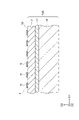
- the resonator 31 has, for example, a piezoelectric body 3 (see FIG. 6, etc.), an IDT electrode 5 positioned on the upper surface 3a of the piezoelectric body 3, and a pair of reflectors 35.
- the resonator 31 may be regarded as including the elastic wave device 1 or may be regarded as being included in the device 1 .
- Resonator 31 also includes piezoelectric body 3 (and other layers that affect acoustic waves), as described above.
- the combination of the IDT electrode 5 and the pair of reflectors 35 may be expressed as the resonator 31 .
- the pair of reflectors 35 is composed of, for example, the same conductor layer as the conductor layer that constitutes the IDT electrode 5 . In a mode in which an additional film that overlaps all or part of the IDT electrode 5 is provided, an additional film that overlaps all or part of the reflector 35 may be provided.
- a pair of reflectors 35 are located on both sides of the IDT electrode 5 in the acoustic wave propagation direction. Each reflector 35 may be, for example, electrically floating or given a reference potential.
- Each reflector 35 is formed, for example, in a lattice shape. That is, reflector 35 includes a pair of busbars 37 facing each other and a plurality of strip electrodes 39 extending between the pair of busbars 37 . As with the plurality of electrode fingers 11, the plurality of strip electrodes 39 may actually be provided in a larger number than shown.
- the busbar 37 has, for example, substantially the same configuration as the busbar 9 of the IDT electrode 5 , and the description of the busbar 9 may be applied to the busbar 37 .
- the position of the bus bar 37 in the D2 direction may be, for example, an appropriate position outside the gap region RG. In the illustrated example, the bus bar 37 is located within the arrangement range of the intervening electrode 41 in the D2 direction.
- the width (D2 direction) of the busbar 37 may be smaller than, equal to, or larger than the width of the busbar 9 .
- the busbar 37 When the busbar 9 is inclined in the elastic wave propagation direction, the busbar 37 may be inclined in the same manner as the busbar 9 or may be parallel to the elastic wave propagation direction.
- the schematic configuration of the plurality of strip electrodes 39 is similar to the schematic configuration of the electrode fingers 11 of the IDT electrodes 5 except that they are bridged over a pair of busbars 37 .
- the description of the electrode fingers 11 may be incorporated into the strip electrodes 39 as appropriate.
- the plurality of strip electrodes 39 are arranged in the acoustic wave propagation direction so as to follow the arrangement of the plurality of electrode fingers 11 .
- the pitch of the plurality of strip electrodes 39 and the pitch between the electrode fingers 11 adjacent to the reflector 35 and the strip electrodes 39 adjacent to the IDT electrode 5 are, for example, the same as the pitch of the plurality of electrode fingers 11 .
- the specific planar shape of the strip electrode 39 (from another point of view, the change in width (length in the D1 direction) according to the position in the D2 direction) is arbitrary.
- the strip electrode 39 has a main portion 39a and a widened portion 39b, similar to the electrode finger 11. As shown in FIG.
- the main portion 39a overlaps the main portion 11a of the electrode finger 11 in the D2 direction.
- the widened portion 39b overlaps the widened portion 39b of the electrode finger 11 in the D2 direction.
- the description of the main portion 11a and the widened portion 11b may be used for the main portion 39a and the widened portion 39b.
- the reflector 35 does not have a structure corresponding to the intervening electrode 41 .
- the reflector 35 may have a structure corresponding to the intervening electrode 41 .
- FIG. 9 is a circuit diagram schematically showing the configuration of the branching filter 101 (for example, duplexer).
- the branching filter 101 for example, duplexer.
- the comb-teeth electrode 7 is schematically shown in a bifurcated fork shape, and the reflector 35 is a line with both ends bent. is represented by
- the branching filter 101 includes, for example, a transmission filter 109 that filters a transmission signal from the transmission terminal 105 and outputs it to the antenna terminal 103, and a reception signal that is filtered from the antenna terminal 103 and outputs it to a pair of reception terminals 107. and a reception filter 111 .
- the transmission filter 109 is configured by, for example, a ladder-type filter configured by connecting a plurality of resonators 31 (series resonators 31S and parallel resonators 31P) in a ladder-type manner. That is, the transmission filter 109 includes a plurality of (one possible) series resonators 31S connected in series between the transmission terminal 105 and the antenna terminal 103, the series line (serial arm) and the reference potential section ( symbol omitted) and a plurality of parallel resonators 31P (parallel arm) connected to each other.
- the reception filter 111 includes, for example, a resonator 31 and a multimode filter (including a double mode filter) 113 .
- the multimode filter includes a dual mode filter.
- the multimode filter 113 has a plurality of (three in the illustrated example) IDT electrodes 5 arranged in the acoustic wave propagation direction, and a pair of reflectors 35 arranged on both sides thereof.
- At least one of the multiple resonators of the transmission filter 109 may include the elastic wave device 1 (IDT electrode 5) according to the embodiment.
- the transmission filter 109 is positioned on the device 1 and the upper surface 3a of the piezoelectric body 3 of the device 1, and the one IDT electrode 5 and the ladder type and one or more other IDT electrodes (in the illustrated example, the other IDT electrodes are also the IDT electrodes 5 according to the embodiment) that are connected to to form a ladder-type filter.
- At least one of the multiple IDT electrodes of the multimode filter 113 may include the elastic wave device 1 (IDT electrode 5) according to the embodiment.
- the multimode filter 113 is positioned on the device 1 and the upper surface 3a of the piezoelectric body 3 of the device 1, and is attached to the one IDT electrode 5.
- it has one or more other IDT electrodes (in the illustrated example, the other IDT electrodes are also the IDT electrodes 5 according to the embodiment) arranged in the elastic wave propagation direction and constituting a multimode filter. .
- each of the branching filter 101, the transmission filter 109 (ladder filter), the reception filter 111, and the multimode filter 113 may be regarded as including the device 1 according to the embodiment, or the device 1 may be taken to be included.
- a plurality of IDT electrodes 5 (and reflectors 35) of the branching filter 101 may be provided on one piezoelectric body 3 (substrate), or may be dispersedly provided on two or more piezoelectric bodies 3.
- the plurality of resonators 31 forming the transmission filter 109 may be provided on the same piezoelectric body 3 .
- the resonator 31 and the multimode filter 113 that constitute the reception filter 111 may be provided on the same piezoelectric body 3, for example.
- the transmission filter 109 and the reception filter 111 may be provided on the same piezoelectric body 3 or may be provided on different piezoelectric bodies 3 .
- a plurality of series resonators 31S may be provided on the same piezoelectric body 3, and a plurality of parallel resonators 31P may be provided on another same piezoelectric body 3.
- FIG. 9 is just an example of the configuration of the branching filter 101.
- the receive filter 111 may be configured by a ladder-type filter like the transmit filter 109 .
- the transmit filter 109 may have a multimode filter 113 .
- the demultiplexer 101 is not limited to a duplexer, and may be, for example, a diplexer or a multiplexer including three or more filters.
- FIG. 10 is a block diagram showing a main part of a communication device 151 as an application example of the elastic wave device 1. As shown in FIG. The communication device 151 performs wireless communication using radio waves, and includes the branching filter 101 .
- a radio signal (radio waves) received by the antenna 159 is converted into an electric signal (received signal RS) by the antenna 159 and input to the branching filter 101 (antenna terminal 103).
- the demultiplexer 101 removes unnecessary components outside the pass band for reception from the input reception signal RS, and outputs the signal from the reception terminal 107 to the amplifier 161 .
- the output reception signal RS is amplified by an amplifier 161 and a bandpass filter 163 removes unnecessary components outside the passband for reception. Then, the reception signal RS is subjected to frequency reduction and demodulation by the RF-IC 153 to be a reception information signal RIS.
- the transmitted information signal TIS and the received information signal RIS may be low-frequency signals (baseband signals) containing appropriate information, such as analog audio signals or digitized audio signals.
- the pass band of the radio signal may be set appropriately and may comply with various known standards.
- the modulation method may be phase modulation, amplitude modulation, frequency modulation, or a combination of two or more of these.
- the direct conversion system is exemplified as the circuit system, other appropriate systems may be used. For example, a double superheterodyne system may be used.
- FIG. 10 schematically shows only the main part, and low-pass filters, isolators, etc. may be added at appropriate positions, and the positions of amplifiers, etc. may be changed.
- the elastic wave device 1 may be used in various modes other than the modes illustrated above.
- the elastic wave device 1 may be used as a two-port resonator or as a transversal filter.
- FIG. 11 is a diagram showing characteristics of resonators according to the first comparative example and the first example.
- the horizontal axis indicates frequency.
- the vertical axis indicates the impedance phase.
- a line LC1 indicates the characteristics of the first comparative example.
- a line LE1 indicates the characteristics of the first embodiment.
- the resonator 31 has a resonance frequency at which the absolute value of impedance is a minimum value and an anti-resonance frequency at which the absolute value of impedance is a maximum value.
- the range between the resonance frequency and the anti-resonance frequency the closer the impedance phase is to 90°, the better the characteristics of the resonator 31 are. Outside the above range, the characteristics of the resonator 31 are said to be better when the phase of the impedance is closer to -90°.
- the range on the horizontal axis generally corresponds to the range between the resonance frequency and the anti-resonance frequency.
- the IDT electrode 5 has the same configuration as the IDT electrode 5A according to the first example shown in FIG.
- the first comparative example has a configuration in which the plurality of connecting portions 45 are eliminated from the first embodiment.
- each comb tooth electrode 7 it is assumed that the plurality of bar electrodes 43 and the bus bars 9 are at the same potential (electrically connected).
- the number and magnitude of spurious signals are reduced compared to the first comparative example. That is, it was confirmed that the spurious response was reduced by discontinuously providing a plurality of connecting portions 45 in the D2 direction.
- ⁇ Piezoelectric material Material: LT Cut angle: 50° rotation Y cut X propagation Thickness: 0.65 ⁇ m - Low sound speed layer (intermediate layer 17): Material: SiO2 Thickness: 0.22 ⁇ m - High sound velocity layer (support substrate 15): Material: Si Thickness: Sufficient thickness (200 ⁇ m) for pitch p ⁇ IDT electrode: Material: Laminated structure of Ti and Al Thickness: Ti: 60 ⁇ Al: 1400 ⁇ Electrode finger: Number: 250 Pitch: 1.03 ⁇ m Main duty: 0.50 Duty of widening part: 0.60 Length of one widened portion (D2 direction): 1.0 ⁇ m Width of intersection region R0: 40p Gap G1 length (D2 direction): 0.3 ⁇ m Bar electrode: Number: 8 Width (D2 direction): 0.25p Distance between bar electrodes (width of slit region S1): 0.25p ⁇ Reflector:
- FIG. 12 is a diagram showing the characteristics of the resonators according to the first to third examples, similar to FIG. 11.
- line LE1 indicates the characteristics of the first embodiment and is the same as line LE1 shown in FIG.
- Lines LE2 and LE3 show the characteristics of the second and third embodiments, respectively.
- the IDT electrode 5 has the same configuration as the IDT electrode 5B according to the second example shown in FIG. 3A. That is, in the first embodiment, the size of the V-shape in the D2 direction is approximately 2p, whereas in the second embodiment, the size of the V-shape in the D2 direction is approximately 1p.
- the third embodiment has the same configuration as the IDT electrode 5C according to the third embodiment shown in FIG. 3B. However, it is assumed that the connection portion 45 is eliminated from the I-shaped portion including the Y-shaped portion, and that the plurality of bar electrodes 43 and the bus bars 9 are set to the same potential (electrically connected to each other).
- the second embodiment has less spurious than the first embodiment
- the first embodiment has less spurious than the third embodiment. That is, the larger the change in the position of the connecting portion 45 in the D2 direction with respect to the position in the D1 direction, the more spurious is reduced. It should be noted that the first embodiment is easier to fabricate than the second embodiment.
- FIG. 13 is a diagram similar to FIG. 11 showing the characteristics of the resonators according to the second and third comparative examples and the fourth example.
- lines LC2, LC3 and LE4 indicate the characteristics of the second and third comparative examples and the fourth example, respectively.
- the IDT electrode 5 has the same configuration as the IDT electrode 5D according to the fourth example shown in FIG. 3C. That is, in the fourth embodiment, the width of the electrode fingers 11 is made constant over the entire length of the electrode fingers 11 in the first embodiment.
- the intervening electrode 41 is eliminated by expanding the bus bar 9 to the arrangement area of the intervening electrode 41 in the fourth embodiment.
- the third comparative example is obtained by eliminating the plurality of connection portions 45 in the fourth embodiment.
- the fourth embodiment has less spurious than the second and third comparative examples. As a result, even if the IDT electrode 5 does not use the piston mode, it was confirmed that the spurious response is reduced by discontinuously arranging the plurality of connecting portions 45 in the D2 direction.
- a simulation calculation was also performed for a comparative example in which the thickness of the bus bar was reduced in the second comparative example. From another point of view, a simulation calculation was also performed for a comparative example in which the intervening electrode 41 was not provided and the sound velocity in the region corresponding to the intervening region RI was increased. As a result, when the thickness of the bus bar is reduced, the spurious effect can be reduced, but the effect is not as good as that of the example. From this, it was confirmed that the effect of reducing the spurious by the intervening electrode 41 is the effect as a reflector against the spurious in the transverse mode.
Landscapes
- Physics & Mathematics (AREA)
- Acoustics & Sound (AREA)
- Surface Acoustic Wave Elements And Circuit Networks Thereof (AREA)
Abstract
IDT電極は、以下の部位を有している。第1バスバー。第1バスバーに対向する第2バスバー。第1バスバーにそれぞれ電気的に接続されている複数の第1電極指。第2バスバーにそれぞれ電気的に接続され、複数の第1電極指と弾性波伝搬方向に交互に配列されている複数の第2電極指。第1バスバーの間と複数の第1電極指との間に介在し、第1バスバーに対して並列に延びているとともに互いに並列に延びている複数のバー電極。第1バスバーと第1バスバーに隣り合うバー電極との間に介在して両者を接続している接続部と、隣り合うバー電極の間に介在して両者を接続している接続部と、を含む複数の接続部。複数の接続部の少なくとも一部は、複数の電極指の延在方向に対して、不連続に配置されている。
Description
本開示は、弾性波(acoustic wave)から電気信号への変換、及び電気信号から弾性波への変換の少なくとも一方が可能な弾性波装置、当該弾性波装置を含むフィルタ、当該フィルタを含む分波器、並びに当該分波器を含む通信装置に関する。
弾性波装置として、圧電層と、圧電層上に位置するIDT(Interdigital Transducer)電極とを有するものが知られている(例えば、下記特許文献1)。IDT電極は、1対の櫛歯電極を有する。各櫛歯電極は、バスバーと、バスバーから互いに並列に延びる複数の電極指とを有する。1対の櫛歯電極は、互いに噛み合うように配置される。特許文献1では、バスバーが延びる方向に配列された複数の開口をバスバーに設けたIDT電極が開示されている。
本開示の一態様に係る弾性波装置は、第1面を有している圧電体と、前記第1面上に位置するIDT電極と、を有している。前記IDT電極は、第1バスバーと、第2バスバーと、複数の第1電極指と、複数の第2電極指と、複数のバー電極と、複数の接続部と、を有している。前記第2バスバーは、前記第1バスバーと対向する。前記複数の第1電極指は、前記第1バスバーにそれぞれ電気的に接続されている。前記複数の第2電極指は、前記第2バスバーにそれぞれ電気的に接続され、弾性波伝搬方向に前記複数の第1電極指と交互に配列されている。前記複数のバー電極は、前記第1バスバーの間と前記複数の第1電極指との間に介在し、前記第1バスバーに対して並列に延びているとともに互いに並列に延びている。前記複数の接続部は、前記第1バスバーと前記第1バスバーに隣り合うバー電極との間に介在して両者を接続している接続部と、隣り合うバー電極の間に介在して両者を接続している接続部と、を含む。前記複数の接続部の少なくとも一部は、前記複数の第1電極指の延在方向に対して、不連続に配置されている。
本開示の一態様に係るフィルタは、上記弾性波装置と、前記第1面上に位置しており、前記IDT電極とラダー型に接続されてラダー型フィルタを構成している1以上の他のIDT電極と、を有している。
本開示の一態様に係るフィルタは、上記弾性波装置と、前記第1面上に位置しており、前記IDT電極に対して前記弾性波伝搬方向に並べられて多重モード型フィルタを構成している1以上の他のIDT電極と、を有している。
本開示の一態様に係る分波器は、アンテナ端子と、前記アンテナ端子に接続されている送信フィルタと、前記アンテナ端子に接続されている受信フィルタと、を有している。前記送信フィルタ及び受信フィルタの少なくとも一方が、上記のいずれかのフィルタによって構成されている。
本開示の一態様に係る通信装置は、上記の分波器と、前記アンテナ端子に接続されているアンテナと、前記送信フィルタ及び前記受信フィルタに接続されているIC(Integrated Circuit)と、を有している。
以下、本開示に係る実施形態について、図面を参照して説明する。以下の説明で用いられる図は模式的なものである。従って、例えば、図面上の寸法比率等は現実のものとは必ずしも一致していない。寸法比率等が図面同士で一致しないこともある。特定の形状又は寸法等が誇張されて示されることもある。
本開示に係る弾性波装置は、いずれの方向が上方または下方とされてもよい。ただし、以下では、便宜的に、D1軸、D2軸およびD3軸からなる直交座標系を定義するとともに、D3軸の正側を上方として、上面または下面等の用語を用いることがある。また、平面視または平面透視という場合、特に断りがない限りは、D3方向に見ることをいう。なお、D1軸は、後述する圧電体の上面に沿って伝搬する弾性波の伝搬方向に平行になるように定義され、D2軸は、圧電体の上面に平行かつD1軸に直交するように定義され、D3軸は、圧電体の上面に直交するように定義されている。
<弾性波装置>
(弾性波装置の概要)
図1は、実施形態に係る弾性波装置1(以下、単に「装置1」ということがある。)の要部の構成を示す平面図である。
(弾性波装置の概要)
図1は、実施形態に係る弾性波装置1(以下、単に「装置1」ということがある。)の要部の構成を示す平面図である。
装置1は、例えば、圧電体3(後述する図6等を参照)と、圧電体3の上面3a(第1面の一例)上に位置しているIDT電極5とを有している。図1は、上面3aの平面視となっている。ただし、圧電体3に係る符号及び上面3aの外縁等の図示は省略されている。
IDT電極5に電圧が印加されることによって、圧電体3の交差領域R0(IDT電極5のD2方向中央側の領域)をD1方向に伝搬する弾性波が励振される。及び/又は、弾性波が交差領域R0をD1方向に伝搬することによって、圧電体3に電荷が生成され、IDT電極5に電圧が印加される。装置1は、例えば、このような弾性波と電圧(電気信号)との間の変換を利用する共振子及び/又はフィルタを構成してよい。なお、以下において、D1方向を弾性波伝搬方向又は伝搬方向等ということがある。
IDT電極5は、圧電体3の上面3aに重なる導体層によって構成されている。また、IDT電極5は、1対の櫛歯電極7を含んでいる。各櫛歯電極7は、例えば、バスバー9と、バスバー9に電気的に接続されている複数の電極指11と、を含んでいる。1対の櫛歯電極7は、複数の電極指11が互いに噛み合うように(交差するように)配置されている。上記の交差領域R0は、一方の櫛歯電極7の複数の電極指11と他方の櫛歯電極7の複数の電極指11とが弾性波伝搬方向に重なる領域である。
一般に、各櫛歯電極7において、複数の電極指11は、バスバー9から延びる。すなわち、両者は直接的に接続されている。一方、本実施形態においては、各櫛歯電極7は、バスバー9と複数の電極指11との間に介在する介在電極41を有している。これにより、例えば、後に詳述するように、横モードのスプリアスを低減することができる。
装置1において、介在電極41に係る構成以外の構成は、種々の態様とされてよく、例えば、公知の態様とされても構わない。このような公知の態様とされても構わない構成については、適宜に説明を省略する。
実施形態の説明では、概ね、以下の順に説明を行う。
・IDT電極5(主として介在電極41以外の部分)(図1)
・介在電極41(図2)
・IDT電極5(特に介在電極41)の種々の具体例(図2~図5)
・弾性波の速度プロファイル(図1)
・圧電体を含む基板の種々の構成例(図6及び図7)
・弾性波装置のその他の構成
・弾性波装置のまとめ
・IDT電極5(主として介在電極41以外の部分)(図1)
・介在電極41(図2)
・IDT電極5(特に介在電極41)の種々の具体例(図2~図5)
・弾性波の速度プロファイル(図1)
・圧電体を含む基板の種々の構成例(図6及び図7)
・弾性波装置のその他の構成
・弾性波装置のまとめ
(IDT電極)
バスバー9は、例えば、概略、一定の幅で弾性波の伝搬方向(D1方向)に直線状に延びる長尺状に形成されている。1対のバスバー9は、弾性波の伝搬方向に直交する方向(D2方向)において互いに対向している。各バスバー9の交差領域R0側の縁部は、例えば、直線状である。また、1対のバスバー9において、交差領域R0側の縁部は、例えば、互いに平行(「平行」の概念は「曲線」に拡張されてよい。)である。別の観点では両縁部の距離(D2方向)はD1方向の位置によらずに一定である。
バスバー9は、例えば、概略、一定の幅で弾性波の伝搬方向(D1方向)に直線状に延びる長尺状に形成されている。1対のバスバー9は、弾性波の伝搬方向に直交する方向(D2方向)において互いに対向している。各バスバー9の交差領域R0側の縁部は、例えば、直線状である。また、1対のバスバー9において、交差領域R0側の縁部は、例えば、互いに平行(「平行」の概念は「曲線」に拡張されてよい。)である。別の観点では両縁部の距離(D2方向)はD1方向の位置によらずに一定である。
図示の例とは異なり、バスバー9は、幅が変化したり、弾性波の伝搬方向に対して傾斜したりしていてもよい。また、各バスバー9において、交差領域R0側の縁部は、曲線状であってもよいし、互いに交差する複数の直線からなる形状であってもよい。また、1対のバスバー9において、互いに対向している縁部同士の距離は、D1方向の位置に応じて変化してもよい。
バスバー9の長さ(D1方向)は、例えば、1対の櫛歯電極7における複数の電極指11のピッチp及び本数の積と概ね同等とされてよい。バスバー9の幅(D2方向)は任意である。一般に、バスバー9の幅は、電極指11の幅(D1方向)よりも大きい。例えば、バスバー9の幅は、1p以上とされてよい。
複数の電極指11は、例えば、互いに同じ形状及び寸法を有している。図示の例とは異なり、複数の電極指11は、互いに異なる形状及び/又は寸法を有していても構わない。例えば、複数の電極指11は、互いに長さが異なっていてもよい。すなわち、IDT電極5は、いわゆるアポダイズが施されたものであってもよい。
各電極指11は、例えば、概略、その中心線が弾性波の伝搬方向に直交する方向(D2方向)に直線状に延びる長尺状に形成されている。電極指11は、一定の幅(D1方向の長さ)で延びていてもよいし、長さ方向(D2方向)の位置に応じて幅が変化していてもよい(図示の例)。図1に示す例では、電極指11は、先端と根元側とに、他の大部分(主部11a)よりも幅が広い拡幅部11bを有している。これにより、いわゆるピストンモード(又はこれに類似するモード。以下、同様。)が利用され、ひいては、横モードのスプリアスが低減される。なお、本実施形態の説明では、当該態様を前提とした表現をすることがある。
各櫛歯電極7において、複数の電極指11は、弾性波の伝搬方向に配列されている。各櫛歯電極7において、複数の電極指11の先端(又は根元)を結ぶ線(不図示)は、例えば、伝搬方向に平行な直線状である。ただし、図示の例とは異なり、上記線は、伝搬方向に傾斜していてもよいし、曲線状であってもよいし、互いに交差する複数の直線からなる形状であってもよい。なお、上記のようにピストンモードが利用される態様においては、例えば、上記線は、伝搬方向に対して平行な、又は傾斜する、直線状とされてよい。
一方の櫛歯電極7の複数の電極指11と、他方の櫛歯電極7の電極指11とは、弾性波の伝搬方向に交互に配列されている。なお、このようにいうとき、一方の櫛歯電極7の複数の電極指11と、他方の櫛歯電極7の電極指11とは、1本ずつ交互に配列されていてもよいし(図示の例)、2以上の本数ずつ交互に配列されていてもよい。また、いわゆる間引き等によって、特異的な部分が存在していても構わない。実施形態の説明では、1本ずつ交互に配列されている態様を例に取る。
1対の櫛歯電極7における複数の電極指11のピッチp(例えば互いに隣り合う2本の電極指11の中心間距離)は、IDT電極5内において基本的に一定である。なお、IDT電極5は、一部にピッチpに関して特異な部分を有していてもよい。特異な部分としては、例えば、大部分(例えば8割以上)よりもピッチpが狭くなる狭ピッチ部、大部分よりもピッチpが広くなる広ピッチ部、少数の電極指11が実質的に間引かれた間引き部が挙げられる。
実施形態の説明において、ピッチpという場合、特に断りがない限りは、上記のような特異な部分を除いた部分(複数の電極指11の大部分)のピッチをいうものとする。また、特異な部分を除いた大部分の複数の電極指11においても、ピッチが変化しているような場合においては、大部分の複数の電極指11のピッチの平均値をピッチpの値として用いてよい。
電極指11の本数は、IDT電極5(装置1)に要求される電気特性等に応じて適宜に設定されてよい。図1は模式図であることから、電極指11の本数は少なく示されている。実際には、図示よりも多くの電極指11が配列されてよい。例えば、電極指11の本数は100本以上とされてよい。なお、図1は、IDT電極5の一部を抽出して示す図として捉えられてもよい。
一方の櫛歯電極7の各電極指11の先端は、他方の櫛歯電極7の介在電極41(より詳細には最も電極指11側のバー電極43(後述))の縁部とギャップG1を介して対向している。複数のギャップG1のD2方向における長さは、例えば、互いに同一である。当該長さは、適宜に設定されてよく、例えば、0.1p以上0.5p以下とされてよい。
1対の櫛歯電極7に電圧が印加されると、複数の電極指11によって圧電体3の上面3aに電圧が印加され、圧電体3の上面(圧電体3が相対的に厚い場合)又は圧電体3の全体(圧電体3が相対的に薄い場合)が振動する。これにより、上面3aに沿って伝搬する弾性波が励振される。このとき、複数の電極指11によって励振された複数の弾性波は、その半波長が概ねピッチpと同等であるときに、複数の電極指11に直交する方向(D1方向)において互いに同相となり、その振幅が足し合わされる。すなわち、ピッチpを半波長とし、D1方向に伝搬する弾性波が最も励振されやすい。その結果、IDT電極5に印加された電圧のうち、主として、概ねピッチpを半波長とする弾性波の周波数と同等の周波数を有する成分が弾性波に変換される。また、上面3aのうち1対の櫛歯電極7の配置領域に弾性波が生じた場合においては、上記とは逆の原理によって、主として、概ねピッチpを半波長とし、D1方向に伝搬する弾性波が電圧に変換される。このような原理を利用して、共振子又はフィルタが実現される。
装置1においては、適宜なモードの弾性波が利用されてよい。例えば、弾性波は、弾性表面波(SAW:Surface Acoustic Wave)であってよい。SAWとしては、例えば、レイリー波又はリーキー波が利用されてよい。また、弾性波は、薄板状の圧電体を伝搬する板波であってよい。板波としては、例えば、A1モードのラム波、S0モードのラム波及びSH(Shear Horizontal)型の板波が利用されてよい。また、弾性波のモードは、このように明確に特定又は区別できなくてもよい。
電極指11のピッチpは、上記のように、基本的に、意図されている共振周波数と同等の周波数を有している弾性波の半波長である。ピッチpの絶対値を例示すると、0.5μm以上15μm以下である。電極指11の長さ(D2方向)は、例えば、10p以上又は20p以上とされてよく、また、100p以下又は50p以下とされてよい。上記の下限と上限とは、いかようにも組み合わされてよい。
電極指11のピッチpの2倍(2p)に対する電極指11の幅(D1方向)の比(=幅/2p)をデューティー比ということがある。デューティー比は適宜に設定されてよい。例えば、主部11a(若しくは全長に亘って一定の幅を有する電極指11)のデューティー比は、0.40以上又は0.45以上とされてよく、また、0.60以下又は0.55以下とされてよい。上記の上限と下限とは、いかように組み合わされてもよい。また、拡幅部11bのデューティー比は、上記の主部11aのデューティー比よりも大きいことを条件として、0.50以上又は0.55以上とされてよく、また、0.80以下、0.70以下又は0.65以下とされてよい。上記の上限と下限とは、いかようにも組み合わされてよい。
図示の例のように、各電極指11が1つの主部11aと2つの拡幅部11bとを有する構成である態様において、これらの長さ(D2方向)は適宜に設定されてよい。例えば、1つの拡幅部11bの長さは、0.5p以上、0.7p以上又は0.9p以上とされてよく、また、2p以下、1.5p以下又は1.1p以下とされてよい。上記の上限と下限とは、いかようにも組み合わされてよい。
IDT電極5(導体層)の厚さは、例えば、概ね、平面方向(D1-D2平面に平行な方向)の位置によらずに一定である。導体層の厚さは、装置1に要求される特性に応じて適宜に設定されてよい。例えば、導体層の厚さは、0.04p以上0.20p以下、及び/又は50nm以上600nm以下とされてよい。
導体層は、例えば、金属により形成されている。金属は、適宜な種類のものとされてよく、例えば、アルミニウム(Al)又はAlを主成分とする合金(Al合金)である。Al合金は、例えば、Al-銅(Cu)合金である。導体層は、複数の金属層から構成されていてもよい。例えば、導体層は、圧電体3の上面3aに重なるチタン(Ti)からなる比較的薄い層と、その上に重なるAl又はAl合金とによって構成されてよい。Tiは、例えば、Al又はAl合金と圧電体3との接合性の強化に寄与する。
(介在電極)
図2は、図1の領域IIの拡大図である。
図2は、図1の領域IIの拡大図である。
なお、後に例示するように、介在電極41の具体的な形状は種々可能である。図2では、第1例に係る介在電極41Aが例示されている。図2(及び図2に類似する図面)を参照して行う説明において、特に断りがない限り、また、矛盾等が生じない限り、バスバー9、電極指11及び介在電極41は、互いに接続されているもの(1つの櫛歯電極7内のもの)を指す。
介在電極41は、例えば、概略、格子状若しくは網目状に構成されている。具体的には、例えば、介在電極41は、複数(図示の例では8本)のバー電極43及び複数の接続部45の2種の部位を有している。複数のバー電極43は、バスバー9に並列に延びているとともに、互いに並列に延びている。隣り合う2つのバー電極43(又は隣り合うバー電極43及びバスバー9)の間の領域をスリット領域S1と呼称することがある。各接続部45は、スリット領域S1に位置して、隣り合う2つのバー電極43(又は隣り合うバー電極43及びバスバー9)を接続する。
複数の接続部45の少なくとも一部(図示の例では全部)は、電極指11の延在方向(D2方向)に対して不連続に配置されている。すなわち、複数の接続部45の少なくとも一部は、バスバー9から最も電極指11側のバー電極43まで延びるD2方向に平行な直線を構成するように配置されていない。別の観点では、少なくとも1つの接続部45の少なくとも一部は、自己が位置するスリット領域S1以外の少なくとも1つのスリット領域S1(例えば隣のスリット領域S1)における導体(IDT電極5)の非配置領域とD2方向に重なる。
上記のように複数の接続部45を配置することによって、例えば、スプリアスを低減することができる。当該効果について、出願人は、試作品における実測値及びシミュレーション計算によって確認しており、後に、いくつかの例を示す。スプリアスを低減できる原理としては、以下に説明するものが挙げられる。
弾性波は、導体(IDT電極5)の配置領域と非配置領域との境界で反射する。仮に、全ての接続部45がD2方向に平行な直線を構成するように配置されている場合、横モードのスプリアスは、上記直線のD1方向の位置においては、最も電極指11側のバー電極43で反射し、他のD1方向の位置においては、複数のバー電極43(及びバスバー9)それぞれにより反射する。すなわち、反射が生じるD2方向における位置は、基本的に、D1方向の位置によらずに一定である。その結果、横モードのスプリアスは、波長、並びに節及び腹の位置が揃いやすく、ひいては、互いに強め合いやすい。
一方、本実施形態のように複数の接続部45がD2方向に対して不連続に配置されていると、接続部45とD2方向に重なる位置に導体の非配置領域が存在する。この非配置領域とバー電極43との間でも横モードのスプリアスが反射する。また、接続部45の形状によっては、接続部45においても反射が生じる。これらの新たな反射の位置は、D1方向及びD2方向の位置が分散されている。その結果、横モードのスプリアスは、波長、並びに節及び腹の位置が分散され、ひいては、互いに強め合う作用が減じられる。
上記の原理から理解されるように、複数の接続部45がD2方向に対して不連続に配置される限り、複数のバー電極43及び複数の接続部45の数、形状、位置及び寸法等は任意である。例えば、以下のとおりである。
複数のバー電極43の数は、2以上の任意の数とされてよい。2本のバー電極43が設けられていると、当該2本のバー電極43及びバスバー9によって2つのスリット領域S1が構成される。ひいては、互いに異なるスリット領域S1に位置する少なくとも2つの接続部45をD2方向に対して不連続に配置できる。
複数のバー電極43は、例えば、互いに同一の形状及び寸法を有している。また、各バー電極43は、概略、一定の幅で直線状に延びる形状である。別の観点では、バー電極43の縁部又は中心線の形状は、バスバー9の電極指11側の縁部の形状と同じ、及び/又は介在電極41とギャップG1を介して対向している電極指11の先端(着目しているバー電極43が属する櫛歯電極7と噛み合う櫛歯電極7の電極指11の先端)を結ぶ線の形状と同じである。
上記の例示の裏返しとなるが、念のために記載すると、図示の例とは異なり、少なくとも1つのバー電極43は、他の少なくとも1つのバー電極43に対して、互いに異なる形状及び/又は寸法を有していてもよい。バー電極43は、D1方向の位置に応じて幅(D2方向)が変化してもよい。バー電極43の中心線及び/又は縁部は、曲線状であったり、互いに交差する複数の直線を有する形状であったりしてもよい。また、バー電極43の中心線及び/又は縁部の形状は、バスバー9の電極指11側の縁部の形状と異なっていてもよいし、及び/又は介在電極41とギャップG1を介して対向している電極指11の先端を結ぶ線の形状と異なっていてもよい。
バー電極43の長さ(D1方向)は、バスバー9の長さと概ね同等とされてよい。バー電極43の幅は、例えば、バスバー9の幅(D2方向)及び/又は電極指11の幅(D1方向)に対して、小さくてもよいし(図示の例)、同等でもよいし、大きくてもよい。また、例えば、バー電極43の幅は、0.1p以上又は0.2p以上とされてよく、0.5p以下又は0.3p以下とされてよい。上記の下限と上限とは、いかようにも組み合わされてよい。
既述のように、複数のバー電極43は、バスバー9に対して並列に延びているとともに互いに並列に延びている。より詳細には、図示の例では、複数のバー電極43(例えば中心線。以下、同様。)及びバスバー9の電極指11側の縁部は、互いに平行に延びている。別の観点では、これらのD2方向(電極指11の延在方向)における距離は、D1方向(弾性波の伝搬方向)の位置によらずに一定である。複数のバー電極43(及びバスバー9)が延びる方向は、例えば、D1方向である。
図示の例とは異なり、少なくとも1つのバー電極43の一部又は全部は、バスバー9、他の少なくとも1つのバー電極43、及び/又はD1方向に対して傾斜していてもよい。また、その結果、バー電極43は、バスバー9及び/又は他のバー電極43に対して交差する部分を有していてもよい。ただし、この場合、交差する部分の一部を接続部45の一種として捉え、複数のバー電極43は交差していないと捉えてもよい。
複数のバー電極43のピッチ(例えば互いに隣り合う2本のバー電極43の中心間距離)は、例えば、互いに同一である。ただし、少なくとも1つのピッチが他のピッチと異なっていてもよい。また、バー電極43のピッチは、電極指11のピッチpに対して、小さくてもよいし(図示の例)、同等でもよいし、大きくてもよい。バー電極43のピッチは、例えば、0.2p以上又は0.4p以上とされてよく、1p以下又は0.6p以下とされてよい。上記の下限と上限とは、いかようにも組み合わされてよい。
複数のスリット領域S1の幅(D2方向)は、例えば、互いに同一である。ただし、少なくとも1つの幅が他の幅と異なっていてもよい。また、スリット領域S1の幅は、電極指11のピッチpに対して、小さくてもよいし(図示の例)、同等でもよいし、大きくてもよい。例えば、スリット領域S1の幅は、0.1p以上又は0.2p以上とされてよく、0.5p以下又は0.3p以下とされてよい。上記の下限と上限とは、いかようにも組み合わされてよい。
バー電極43のピッチに対するバー電極43の幅の比(後者を前者で割った値。デューティー比)は、例えば、電極指11のデューティー比に対して、小さくてもよいし、同等でもよいし、大きくてもよい。例えば、バー電極43のデューティー比は、0.1以上又は0.4以上とされてよく、0.8以下又は0.6以下とされてよい。上記の下限と上限とは、いかようにも組み合わされてよい。
複数の接続部45の形状及び寸法は、例えば、互いに同一である。そして、複数の接続部45のD2方向に対する不連続性は、複数の接続部45の位置(例えば幾何中心の位置。特に断りが無い限り、以下、同様。)がD2方向に平行な直線上に位置しない(D1方向に互いにずれる)ことによって実現されている。ただし、図示の例とは異なり、複数の接続部45の形状及び寸法は、互いに異なっていてもよい。この場合、D1方向の位置のずれに加えて、又は代えて、複数の接続部45の形状及び/又は寸法の相違によって、D2方向に対する不連続性が実現されてもよい。
接続部45の形状、例えば、D1方向及びD2方向に平行な4辺を有する矩形状(図4A参照)、若しくはD1方向に平行な2辺を有する平行四辺形状(図2の例)、又はこれらのいずれとも言えない形状(例えば図5参照)とされてよい。接続部45のD2方向の長さは、スリット領域S1の幅と同等であり、当該幅については、既述のとおりである。接続部45のD1方向の長さは適宜に設定されてよい。例えば、接続部45のD1方向の長さは、接続部45のD2方向の長さに対して、短くてもよいし、同等でもよいし、長くてもよい。また、例えば、接続部45のD1方向の長さは、0.1p以上、0.3p以上又は0.5p以上とされてよく、また、1p以下、0.8p以下又は0.7p以下とされてよい。上記の下限と上限とは、いかようにも組み合わされてよい。
(IDT電極(特に介在電極)の種々の具体例)
図3A~図5は、IDT電極5(特に介在電極41)の他の具体例を示す平面図である。図3A~図3D及び図5は、図2と同様に、図1の領域IIに相当する範囲を示している。図4A~図4Eは、1対の櫛歯電極7のD1方向における一部の範囲を示している。なお、図3A~図4Eにおいては、直交座標系D1-D2-D3の図示が省略されているが、図2と同様に、図の左右方向がD1方向であり、図の上下方向がD2方向である。
図3A~図5は、IDT電極5(特に介在電極41)の他の具体例を示す平面図である。図3A~図3D及び図5は、図2と同様に、図1の領域IIに相当する範囲を示している。図4A~図4Eは、1対の櫛歯電極7のD1方向における一部の範囲を示している。なお、図3A~図4Eにおいては、直交座標系D1-D2-D3の図示が省略されているが、図2と同様に、図の左右方向がD1方向であり、図の上下方向がD2方向である。
これらの図に例示されている種々の具体例は、主として、複数の接続部45の配置が互いに異なっている。以下、図2から順に、各具体例について説明する。なお、図2に示されているIDT電極5A(介在電極41A)の説明の後においては、基本的に、先に説明されたIDT電極5との相違点について述べる。特に言及が無い事項については、先に説明されたIDT電極5と同様とされたり、先に説明されたIDT電極5から類推されたりしてよい。また、複数の具体例間において、互いに対応する部位が互いに異なる形状を有していても、便宜上、当該部位に同一の符号を用いることがある。
(IDT電極の第1例)
図2に示すIDT電極5A(介在電極41A)では、複数の接続部45は、D2方向に傾斜する直線を構成するように配置されている。当該直線は、例えば、バスバー9から、最も電極指11側のバー電極43まで延びている。また、D1方向において隣り合う2本の直線に着目すると、複数の接続部45は、電極指11側に向かって閉じる(又は開く)V字状に配列されている。図示の例では、複数のV字がD1方向に互いにつながるように配列されている。換言すれば、複数の接続部45は、ジグザグにD1方向に延びる線上に配列されている。なお、図示の例とは異なり、D1方向の特定の位置に1つのV字が位置したり、隣り合うV字が互いに離れていたりしてもよい。
図2に示すIDT電極5A(介在電極41A)では、複数の接続部45は、D2方向に傾斜する直線を構成するように配置されている。当該直線は、例えば、バスバー9から、最も電極指11側のバー電極43まで延びている。また、D1方向において隣り合う2本の直線に着目すると、複数の接続部45は、電極指11側に向かって閉じる(又は開く)V字状に配列されている。図示の例では、複数のV字がD1方向に互いにつながるように配列されている。換言すれば、複数の接続部45は、ジグザグにD1方向に延びる線上に配列されている。なお、図示の例とは異なり、D1方向の特定の位置に1つのV字が位置したり、隣り合うV字が互いに離れていたりしてもよい。
図2の例では、最も電極指11側のスリット領域S1においては、2直線上の2つの接続部45がつながっている、又は1つの接続部45が2直線に共用されている。一方、最もバスバー9側のスリット領域S1においては、2直線上の2つの接続部45は互いに離れている。ただし、図示の例とは異なり、最も電極指11側のスリット領域S1において、2直線状の2つの接続部45は、互いに離れていてもよい。最もバスバー9側のスリット領域S1において、2直線状の2つの接続部45は、互いにつながっていてもよい(2直線に共用されていてもよい。)
なお、最も電極指11側のスリット領域S1において、2直線上の2つの接続部45が互いに離れている場合においても、当該2つの接続部45の距離が大きくない限りは、電極指11側において閉じるV字が構成されていると捉えられてよい。例えば、最も電極指11側の2つの接続部45の間の隙間の大きさ(又は幾何中心同士の距離)が、1.5p以下、1.0p以下又は0.7p以下の場合は、電極指11側において閉じるV字が構成されていると捉えられてよい。バスバー9側において閉じるV字が構成されていると捉える場合についても同様である。また、複数のV字がD1方向に繰り返し配列されている態様において、V字同士がつながっていると捉える場合についても同様である。
複数の接続部45がD2方向に対して傾斜する直線(又は曲線)に沿って配列されている態様において、最も電極指11側に位置する接続部45、及び最もバスバー9側に位置する接続部45のD1方向における位置は適宜に設定されてよい。例えば、最も電極指11側に位置する接続部45は、自己が属する櫛歯電極7の電極指11のD1方向における位置に位置していてもよいし(図3Aの左右方向中央側を参照)、他の櫛歯電極7の電極指11のD1方向における位置に位置していてもよいし(図2の例)、前者の位置と後者の位置との間の任意の位置に位置していてもよい。最もバスバー9の側に位置する接続部45についても同様である。
複数の接続部45がD2方向に対して傾斜する直線(又は曲線)に沿って配列されている態様において、当該直線の傾斜角は適宜に設定されてよい。別の観点では、V字のD1方向における大きさは適宜に設定されてよい。さらに別の観点では、上記直線上における最も電極指11側に位置する接続部45と、最もバスバー9側に位置する接続部45とのD1方向における距離(相対位置)は適宜に設定されてよい。さらに別の観点では、複数のV字の配列のピッチは適宜に設定されてよい。
例えば、直線状(又は曲線状)に配列された複数の接続部45の幾何中心を連ねた線を基準として、直線又はV字のD1方向における配置範囲を考える(他の具体例において直線又はV字等の配置範囲について説明するときも同様とする。)。このとき、1つの直線のD1方向における配置範囲は、0.1p以上又は0.2p以上とされてよく、また、2.0p以下、1.5p以下又は1.2p以下とされてよい。上記の下限と上限とは、いかようにも組み合わされてよい。図2の例では、1つの直線のD1方向における配置範囲は、概ね1p(例えば0.8p以上1.2p以下)とされている。また、別の観点では、図2の例では、V字のD1方向における配置範囲は、概ね2p(例えば1.8p以上2.2p以下)とされている。
直線状(又は曲線状)に配列された複数の接続部45の-D1側又は+D1側の縁部に着目する。このとき、当該縁部は、例えば、D1方向に傾斜する同一直線上(又は同一曲線上)に位置している(図4Cのように階段状になっていない。)。換言すれば、複数の接続部45の-D1側の縁部及び/又は+D側の縁部は、互いに滑らかにつながっているかのように構成されている(厳密にはバー電極43が介在している。)。なお、複数の接続部45の配列がV字又は他の形状をなすいずれの態様においても、-D1側の縁部及び/又は+D側の縁部は、滑らかにつながっているかのように構成されていてもよいし、そうでなくてもよい。
直線状(又は曲線状)に配列された複数の接続部45において、隣り合う接続部45同士は、一部同士がD2方向に重なっていてもよいし(図2の例)、重なっていなくてもよい(図4A及び図4Eを参照)。前者の場合における重なる量は、任意であり、例えば、1つの接続部45のD1方向における長さの半分に対して、小さくてもよいし、同等でもよいし、大きくてもよい。後者の場合における2つの接続部45の距離は任意であり、例えば、当該距離は0でもよいし(図4A及び図4Eの例)、0よりも大きくてもよい。
(IDT電極の第2例)
図3Aに示す介在電極41B(IDT電極5B)は、図2の介在電極41Aと同様に、V字状に配列された複数の接続部45を有している。ただし、介在電極41Bでは、V字のD1方向における大きさが介在電極41Aよりも小さくされている。別の観点では、D1方向の所定の長さ範囲において、V字を繰り返し配列する数が多くなっている。具体的には、介在電極41Bでは、1つの直線のD1方向における配置範囲は、概ね0.5p(例えば0.3p以上0.7p以下)とされている。また、別の観点では、図3Aの例では、V字のD1方向における配置範囲は、概ね1p(例えば0.8p以上1.2p以下)とされている。
図3Aに示す介在電極41B(IDT電極5B)は、図2の介在電極41Aと同様に、V字状に配列された複数の接続部45を有している。ただし、介在電極41Bでは、V字のD1方向における大きさが介在電極41Aよりも小さくされている。別の観点では、D1方向の所定の長さ範囲において、V字を繰り返し配列する数が多くなっている。具体的には、介在電極41Bでは、1つの直線のD1方向における配置範囲は、概ね0.5p(例えば0.3p以上0.7p以下)とされている。また、別の観点では、図3Aの例では、V字のD1方向における配置範囲は、概ね1p(例えば0.8p以上1.2p以下)とされている。
(IDT電極の第3例)
図3Bに示す介在電極41C(IDT電極5C)では、複数の接続部45が電極指11側に開くY字状に配置されている。この例に示されるように、複数の接続部45は、D2方向に平行な直線状に配列される2以上の接続部45を含んでいても構わない。介在電極41Cに関しては、電極指11側に位置する複数(スリット領域S1の数よりも少ない数)の接続部45が電極指11側に開くV字状に配置されていると捉えられてもよい。従って、介在電極41AにおけるV字に関する説明は、適宜に介在電極41CのY字のうちのV字に援用されてよい。Y字のうちのV字状部分を構成するスリット領域S1の数と、Y字のうちのI字状部分を構成するスリット領域S1の数との比率は任意である。
図3Bに示す介在電極41C(IDT電極5C)では、複数の接続部45が電極指11側に開くY字状に配置されている。この例に示されるように、複数の接続部45は、D2方向に平行な直線状に配列される2以上の接続部45を含んでいても構わない。介在電極41Cに関しては、電極指11側に位置する複数(スリット領域S1の数よりも少ない数)の接続部45が電極指11側に開くV字状に配置されていると捉えられてもよい。従って、介在電極41AにおけるV字に関する説明は、適宜に介在電極41CのY字のうちのV字に援用されてよい。Y字のうちのV字状部分を構成するスリット領域S1の数と、Y字のうちのI字状部分を構成するスリット領域S1の数との比率は任意である。
(IDT電極の第4例)
図3Cに示すIDT電極5Cでは、複数の電極指11がその全長に亘って一定の幅で延びている。図3Cの例では、介在電極41として、図2の介在電極41Aが例示されている。ただし、全長に亘って一定の幅で延びる電極指11は、他の介在電極41の具体例と組み合わされてもよい。同様に、拡幅部11bを有する電極指11は、いずれの介在電極41の具体例と組み合わされてもよい。
図3Cに示すIDT電極5Cでは、複数の電極指11がその全長に亘って一定の幅で延びている。図3Cの例では、介在電極41として、図2の介在電極41Aが例示されている。ただし、全長に亘って一定の幅で延びる電極指11は、他の介在電極41の具体例と組み合わされてもよい。同様に、拡幅部11bを有する電極指11は、いずれの介在電極41の具体例と組み合わされてもよい。
(IDT電極の第5例)
図3Dに示すIDT電極5Eは、いわゆるダミー電極25を有している。複数のダミー電極25は、介在電極41(より詳細には最も電極指11側のバー電極43)から複数の電極指11と並列に延びている。一方の櫛歯電極7のダミー電極25の先端は、他方の櫛歯電極7の電極指11の先端とギャップG1を介して対向している。
図3Dに示すIDT電極5Eは、いわゆるダミー電極25を有している。複数のダミー電極25は、介在電極41(より詳細には最も電極指11側のバー電極43)から複数の電極指11と並列に延びている。一方の櫛歯電極7のダミー電極25の先端は、他方の櫛歯電極7の電極指11の先端とギャップG1を介して対向している。
ダミー電極25の形状は適宜に設定されてよい。図示の例では、ダミー電極25の形状は、概略、一定の幅で弾性波の伝搬方向に直交する方向に突出する形状とされている。また、図示の例では、ダミー電極25の幅は、拡幅部11bを有さない電極指11の幅(又は拡幅部11bを有する電極指11の主部11aの幅)と同じとされている。
図示の例とは異なり、ダミー電極25の幅は、ギャップG1側及び/又はバスバー9側の一部が拡幅していてもよい。電極指11及びダミー電極25の拡幅部の有無の組み合わせは任意である。例えば、図示の例の他、拡幅部を有する電極指11と拡幅部を有さないダミー電極25との組み合わせ、拡幅部を有する電極指11と拡幅部を有するダミー電極25との組み合わせ、拡幅部を有さない電極指11と拡幅部を有するダミー電極25との組み合わせが採用されてもよい。また、拡幅部を有する電極指11と拡幅部を有さないダミー電極25との組み合わせにおいて、ダミー電極25の幅は、例えば、主部11aの幅と同等であってもよいし、拡幅部11bの幅と同等であってもよい。
図3Dの例では、介在電極41として、図2の介在電極41Aが例示されている。ただし、ダミー電極25は、他の介在電極41の具体例と組み合わされてもよい。同様に、ダミー電極25を有さない態様は、いずれの介在電極41の具体例に適用されてもよい。
(IDT電極の第6例)
図4Aに示す介在電極41F(IDT電極5F)では、複数の接続部45は、図2の介在電極41Aと同様に、D2方向に傾斜する直線状に配列されている。ただし、複数の接続部45は、電極指11側に開くV字状ではなく、D1方向の一方側(図4Aの右側)に開くV字状に配列されている。別の観点では、複数の接続部45は、D2方向に対して互いに逆側に傾斜するとともに互いに交差する2直線に沿って配列されている。V字が開く方向は、1対の櫛歯電極7同士で、同一であってもよいし(図示の例)、異なっていてもよい。特に図示しないが、複数の接続部45は、順に交差する3つ以上の直線(ジグザグの経路)に沿って配置されていてもよい。直線が交差する位置では、2つの接続部45が位置しているが、1つの接続部45のみが位置してもよい。
図4Aに示す介在電極41F(IDT電極5F)では、複数の接続部45は、図2の介在電極41Aと同様に、D2方向に傾斜する直線状に配列されている。ただし、複数の接続部45は、電極指11側に開くV字状ではなく、D1方向の一方側(図4Aの右側)に開くV字状に配列されている。別の観点では、複数の接続部45は、D2方向に対して互いに逆側に傾斜するとともに互いに交差する2直線に沿って配列されている。V字が開く方向は、1対の櫛歯電極7同士で、同一であってもよいし(図示の例)、異なっていてもよい。特に図示しないが、複数の接続部45は、順に交差する3つ以上の直線(ジグザグの経路)に沿って配置されていてもよい。直線が交差する位置では、2つの接続部45が位置しているが、1つの接続部45のみが位置してもよい。
複数の接続部45が構成する2つ(又はそれ以上)の直線の長さ及び/又は傾斜角は、互いに同等であってもよいし(図示の例)、互いに異なっていてもよい。また、介在電極41Aの説明で述べたように、直線状に配列された複数の接続部45の-D1側又は+D1側の縁部は、同一直線上に位置してもよいし(滑らかにつながってもよいし)、位置しなくてもよい。図4Aの例では、後者が採用されており、複数の接続部45の縁部は階段状を呈している。また、介在電極41Aの説明で述べたように、直線状に配列された複数の接続部45において、互いに隣り合う接続部45は、一部同士がD2方向に重なってもよいし、重ならなくてもよい。図4Aの例では、後者であり、より詳細には、互いに隣り合う接続部45は、D1方向に投影したときに互いに隣接している(両者の距離は0である。)。
(IDT電極の第7例)
図4Bに示す介在電極41G(IDT電極5G)では、複数の接続部45は、市松模様をなすように配置されている。また、別の観点では、複数の接続部45は、D2方向に傾斜する互いに平行な複数の直線状に配置され、かつ複数の直線は、一部同士がD2方向に互いに重なっている。
図4Bに示す介在電極41G(IDT電極5G)では、複数の接続部45は、市松模様をなすように配置されている。また、別の観点では、複数の接続部45は、D2方向に傾斜する互いに平行な複数の直線状に配置され、かつ複数の直線は、一部同士がD2方向に互いに重なっている。
(IDT電極の第8例)
図4Cに示す介在電極41H(IDT電極5H)では、複数の接続部45は、D2方向に対して傾斜する互いに平行な複数の直線状に配置されている。ただし、図4Bとは異なり、複数の直線は、D1方向の配置範囲が互いに異なっており、D2方向に互いに重なっていない。
図4Cに示す介在電極41H(IDT電極5H)では、複数の接続部45は、D2方向に対して傾斜する互いに平行な複数の直線状に配置されている。ただし、図4Bとは異なり、複数の直線は、D1方向の配置範囲が互いに異なっており、D2方向に互いに重なっていない。
(IDT電極の第9例)
図4Dに示す介在電極41I(IDT電極5I)は、図4Cの介在電極41Hと概ね同様の構成を有している。すなわち、複数の接続部45は、D2方向(電極指11の延在方向)に対して傾斜する互いに平行な複数の直線状に配置されている。ただし、図4Cでは、一方の櫛歯電極7の直線と他方の櫛歯電極7における直線とが、D2方向に対して互いに逆側に傾斜したのに対して、図4Dでは、一方の櫛歯電極7の直線と他方の櫛歯電極7における直線とが互いに同一側に傾斜している。
図4Dに示す介在電極41I(IDT電極5I)は、図4Cの介在電極41Hと概ね同様の構成を有している。すなわち、複数の接続部45は、D2方向(電極指11の延在方向)に対して傾斜する互いに平行な複数の直線状に配置されている。ただし、図4Cでは、一方の櫛歯電極7の直線と他方の櫛歯電極7における直線とが、D2方向に対して互いに逆側に傾斜したのに対して、図4Dでは、一方の櫛歯電極7の直線と他方の櫛歯電極7における直線とが互いに同一側に傾斜している。
(IDT電極の第10例)
図4Eに示す介在電極41J(IDT電極5J)は、図4Cの介在電極41Hと概ね同様の構成を有している。すなわち、複数の接続部45は、D2方向(電極指11の延在方向)に対して傾斜する互いに平行な複数の直線状に配置されている。ただし、介在電極41Hとは異なり、介在電極41Jの複数の直線は、市松模様(図4Bの介在電極41G参照)に至らない量で、一部同士がD2方向に互いに重なっている。
図4Eに示す介在電極41J(IDT電極5J)は、図4Cの介在電極41Hと概ね同様の構成を有している。すなわち、複数の接続部45は、D2方向(電極指11の延在方向)に対して傾斜する互いに平行な複数の直線状に配置されている。ただし、介在電極41Hとは異なり、介在電極41Jの複数の直線は、市松模様(図4Bの介在電極41G参照)に至らない量で、一部同士がD2方向に互いに重なっている。
(IDT電極の第11例)
図5に示す介在電極41K(IDT電極5K)において、各スリット領域S1内において互いに隣り合う接続部45と、各スリット領域S1の両側のバー電極43とによって囲まれる領域(導体の非配置領域)を開口領域47と呼称するものとする。複数の開口領域47のうち少なくとも1つ(図示の例では全て)の形状は、楕円状となっている。なお、ここでいう楕円は、数学で定義される楕円でなくてよい。例えば、D1方向の両側の縁部が外側に膨らむ曲線状である場合、楕円状と捉えられてよい。典型的には、楕円は、例えば、円形をD2方向につぶした形状である。また、円形も楕円に含まれてよい。長方形の短辺を外側に曲線状に膨らませた形状も、ここでいう楕円状に含まれてよい。ここでは、図2の介在電極41Aと同様に、複数の接続部45がV字状に配置されている態様を例に取っている。ただし、楕円状の開口領域47は、他の態様に適用されて構わない。
図5に示す介在電極41K(IDT電極5K)において、各スリット領域S1内において互いに隣り合う接続部45と、各スリット領域S1の両側のバー電極43とによって囲まれる領域(導体の非配置領域)を開口領域47と呼称するものとする。複数の開口領域47のうち少なくとも1つ(図示の例では全て)の形状は、楕円状となっている。なお、ここでいう楕円は、数学で定義される楕円でなくてよい。例えば、D1方向の両側の縁部が外側に膨らむ曲線状である場合、楕円状と捉えられてよい。典型的には、楕円は、例えば、円形をD2方向につぶした形状である。また、円形も楕円に含まれてよい。長方形の短辺を外側に曲線状に膨らませた形状も、ここでいう楕円状に含まれてよい。ここでは、図2の介在電極41Aと同様に、複数の接続部45がV字状に配置されている態様を例に取っている。ただし、楕円状の開口領域47は、他の態様に適用されて構わない。
(その他)
複数の接続部45の配置は、図示の例以外にも種々可能である。例えば、複数の接続部45は、X字状に配置されてもよい。既に触れているように、曲線に沿って複数の接続部45が配列されてもよい。
複数の接続部45の配置は、図示の例以外にも種々可能である。例えば、複数の接続部45は、X字状に配置されてもよい。既に触れているように、曲線に沿って複数の接続部45が配列されてもよい。
(速度プロファイル)
図1に戻る。圧電体3の上面3aの平面視において、IDT電極5が配置されている領域は、IDT電極5の構成に基づいて、D2方向において以下の4種の領域に区分することができる。複数の第1電極指(一方の櫛歯電極7の電極指11)と複数の第2電極指(他方の櫛歯電極7の電極指11)とが弾性波伝搬方向に重なる交差領域R0。ギャップG1が位置するギャップ領域RG。介在電極41が位置する介在領域RI。バスバー9が位置するバスバー領域RB。
図1に戻る。圧電体3の上面3aの平面視において、IDT電極5が配置されている領域は、IDT電極5の構成に基づいて、D2方向において以下の4種の領域に区分することができる。複数の第1電極指(一方の櫛歯電極7の電極指11)と複数の第2電極指(他方の櫛歯電極7の電極指11)とが弾性波伝搬方向に重なる交差領域R0。ギャップG1が位置するギャップ領域RG。介在電極41が位置する介在領域RI。バスバー9が位置するバスバー領域RB。
交差領域R0は、一方の櫛歯電極7の電極指11の先端を結ぶ線(不図示)と、他方の櫛歯電極7の電極指11の先端を結ぶ線(不図示)とに挟まれる領域として捉えられてもよい。なお、複数の電極指11の所定部位(例えば先端)を結ぶ線を仮定するときに、電極指11の幅内のいずれの位置を基準にするかで上記線の位置等が異なる場合においては、電極指11の中心線を基準としてよい。
図示の例においては、交差領域R0は、電極指11の幅に基づいて、D2方向において以下の2種(3つ)の領域に区分することができる。複数の主部11aがD1方向に互いに重なる中央領域RC。複数の拡幅部11bがD2方向に互いに重なるエッジ領域RE。これらの幅(D2方向)については、主部11a及び拡幅部11bの説明を参照されたい。
これらの複数の領域は、互いに音速が異なる。ここでいう音速は、例えば、装置1によって利用されるモードの弾性波が圧電体3を伝搬する速度とされてよい。ただし、通常、IDT電極5の形状等に基づいて複数の領域が規定されている場合において、利用される弾性波の具体的なモードの相違に応じて複数の領域の音速の高低関係が逆転することはない。従って、以下に述べる音速の高低の関係を考慮するに際して、いずれのモードの弾性波の音速であるかは特定されなくても構わない。
弾性波の音速は、圧電体3の上面3a上に位置する部材(例えばIDT電極5)の質量の影響を受ける。例えば、各領域において、単位面積当たりの質量が大きいほど音速は低くなる。一方、IDT電極5を構成する導体層の厚さが一定の場合、単位面積に占める導体層の比率が大きいほど、単位面積当たりの質量は大きくなる。従って、IDT電極5を構成する導体層の面積比率が大きい領域ほど音速は低くなる。
従って、図示の例において、音速が低いものから領域名を挙げると、例えば、バスバー領域RB、交差領域R0及びギャップ領域RGである。また、交差領域R0においては、エッジ領域REは、中央領域RCよりも音速が低い。介在領域RIの音速は、バスバー領域RBの音速よりも高い。介在領域RIの音速は、交差領域R0及びギャップ領域RGの音速に対して、低くもよいし、同等でもよいし、高くてもよい。例えば、介在領域RIの音速は、ギャップ領域RGの音速及び中央領域RC(又は電極指11の幅が全長に亘って一定の態様における交差領域R0)の音速よりも低い。
特に図示しないが、交差領域R0の音速は、2段階ではなく、3段階以上で変化してもよい。例えば、中央領域RCは、音速が異なる2種以上の領域を含んでよい。エッジ領域REについても同様である。また、D2方向の位置に対する音速の変化は、段階的なものでなく、連続的なものであってもよい。上述した速度プロファイル(領域間の速度の高低の関係)は、単位面積に占める導体層の比率以外の方法によって実現されてもよい。例えば、IDT電極5の上面又は下面に対して部分的に重なる付加膜(後述)が設けられることによって、当該付加膜が設けられた領域の速度が低くされてよい。また、IDT電極5を構成する導体層が部分的に厚くされることによって、当該厚くされた領域の速度が低くされてよい。また、IDT電極5を構成する導体の配置領域及び非配置領域を問わずに、適宜な位置に絶縁膜が設けられることによって、当該絶縁膜が設けられた領域の速度が低くされてよい。
(圧電体を含む基板の種々の構成例)
IDT電極5が形成される上面3aを有する圧電体3は、例えば、基板の一部又は全部とされてよい。当該基板の構成は、種々の態様とされてよく、例えば、公知の態様とされても構わない。以下に、基板の構成を例示する。
IDT電極5が形成される上面3aを有する圧電体3は、例えば、基板の一部又は全部とされてよい。当該基板の構成は、種々の態様とされてよく、例えば、公知の態様とされても構わない。以下に、基板の構成を例示する。
図6は、基板の第1例としての基板13Aの構成を示す断面図である。図示の断面は、図1のVI-VI線における断面に相当する。
基板13Aは、例えば、支持基板15と、支持基板15の上面に重なっている中間層17と、中間層17の上面に重なっている圧電体3とを有している。ここでは、圧電体3は、圧電膜として構成されている。なお、弾性波装置の構成の説明において、特に断りがない限り、「板」、「層」及び「膜」の語に相違はないものとする。各層の厚さは、例えば、平面方向(D1-D2平面に平行な方向)の位置によらずに一定である。
圧電体3は、例えば、圧電性を有する単結晶によって構成されている。このような単結晶を構成する材料としては、例えば、タンタル酸リチウム(LiTaO3。以下、LTと略すことがある。)、ニオブ酸リチウム(LiNbO3。以下、LNと略すことがある。)及び水晶(SiO2)を挙げることができる。なお、圧電体3は、多結晶によって構成されていても構わない。圧電体3のカット角、平面形状及び各種の寸法は適宜に設定されてよい。例えば、LT又はLNからなる圧電体は、回転YカットX伝搬のものとされてよい。すなわち、弾性波の伝搬方向(D1方向)とX軸とは略一致してよい(例えば両者の差は±10°)。このときの圧電体3の上面3aの法線(D3方向)に対するY軸の傾斜角は適宜に設定されてよい。圧電体3の厚さは、例えば、0.1p以上又は0.3p以上とされてよく、また、2p以下又は1p以下とされてよい。上記の上限と下限とは適宜に組み合わされてよい。
支持基板15は、例えば、基板13Aの強度の向上、温度変化に起因する特性変化の補償(温度補償)、及び圧電体3への弾性波の閉じ込めの少なくとも1つに寄与してよい。強度の向上は、例えば、ある程度の強度を有する材料によって構成された支持基板15の厚さが適宜に設定されることによって実現されてよい。温度補償は、例えば、支持基板15の線膨張率が圧電体3の線膨張率よりも小さいことによって実現されてよい。弾性波の閉じ込めは、例えば、支持基板15の音速が圧電体3(及び/又は中間層17)の音速よりも高いこと、及び/又は支持基板15の音響インピーダンスと中間層17の音響インピーダンスとが異なることによって実現されてよい。
支持基板15の材料及び厚さは、上記のような目的に照らして適宜に設定されてよい。例えば、支持基板15の材料は、シリコン(Si)等の半導体、サファイア(Al2O3)等の単結晶又は酸化アルミニウム質焼結体(Al2O3)等のセラミックとされてよい。支持基板15の厚さは、例えば、1p以上又は3p以上である。また、支持基板15の厚さは、例えば、圧電体3の厚さよりも厚い。
中間層17は、例えば、圧電体3と支持基板15の接合強度の向上、及び圧電体3への弾性波の閉じ込めの少なくとも1つに寄与してよい。接合強度の向上は、例えば、所定の接合手法を用いたときに圧電体3及び支持基板15との接合強度が相対的に高い材料が中間層17の材料として選択されることによって実現されてよい。弾性波の閉じ込めは、例えば、中間層17の音速が圧電体3(及び/又は支持基板15)の音速よりも低いこと、及び/又は中間層17の音響インピーダンスと圧電体3(及び/又は支持基板15)の音響インピーダンスとが異なることによって実現されてよい。
中間層17の材料及び厚さは、上記のような目的に照らして適宜に設定されてよい。例えば、中間層17の材料は、酸化ケイ素(SiO2)とされてよい。中間層17の厚さは、例えば、0.01p以上又は0.1p以上とされてよく、また、2p以下、1p以下又は0.5p以下とされてよい。上記の上限と下限とは、適宜に組み合わされてよい。また、中間層17の厚さは、例えば、支持基板15の厚さよりも薄い。また、中間層17の厚さは、圧電体3の厚さに対して、薄くてもよいし、同等でもよいし、厚くてもよい。
上記のように、中間層17が圧電体3よりも音速が低い低音速層とされる一方で、支持基板15が圧電体3よりも音速が高い高音速層とされてもよい。これにより、例えば、圧電体3から漏れる弾性波を低減できる。
ここでいう音速は、例えば、各材料自体の物性値によって決定される横波音速とされてよい。換言すれば、IDT電極5の配置領域における速度プロファイルで述べた音速とは異なり、IDT電極5の影響は無視されてよい。横波音速は、弾性率を密度で割った値の平方根によって得られる。ただし、中間層17及び支持基板15の音速と比較される圧電体3の音速は、横波音速に代えて、利用されるモードの弾性波の中央領域RC(電極指11の幅が全長に亘って一定の態様では交差領域R0)における音速とされてもよい。また、中間層17及び/又は支持基板15の音速は、利用されるモードの弾性波のエネルギーの漏れに及ぼす影響が相対的に大きいモードのバルク波の音速とされてもよい。
低音速層としての中間層17の材料及び高音速層としての支持基板15の材料の組み合わせは任意である。例えば、これらの材料の組み合わせとしては、上述したSiO2及びSiの組み合わせを挙げることができる。中間層17が低音速層として設けられている場合において、中間層17と圧電体3との接合強度を向上させる層、及び/又は中間層17と支持基板15との接合強度を向上させる比較的薄い層が設けられていてもよい。
図7は、基板の第2例としての基板13Bの構成を示す断面図である。図示の断面は、図1のVI-VI線における断面に相当する。
基板13Bは、既述の基板13Aにおいて、中間層17に代えて多層膜19を設けたものである。多層膜19は、2層以上(図示の例では6層)の音響膜(第1膜21A及び第2膜21B)を有している。複数層の音響膜の材料は、積層方向において互いに隣り合っている(他の音響膜を介さずに互いに重なっている)音響膜同士で互いに異なっている。別の観点では、隣り合う音響膜同士は、音響インピーダンスが互いに異なっている。これにより、例えば、両者の界面においては弾性波の反射率が比較的高くなる。その結果、例えば、圧電体3を伝搬する弾性波の漏れが低減される。なお、図6の基板13Aにおける中間層17及び支持基板15の組み合わせは多層膜の一種と捉えられてよい。図7の基板13Bにおいて、支持基板15を含んで多層膜が定義されてもよい。
多層膜19の音響膜の材料の種類の数及び音響膜の数は適宜に設定されてよい。図示の例では、2種の音響膜(第1膜21A及び第2膜21B)が交互に3層以上(より詳細には6層)で積層されている。また、音響膜の材料も任意である。例えば、第1膜21Aの材料は、二酸化ケイ素(SiO2)とされてよい。第2膜21Bの材料は、五酸化タンタル(Ta2O5)、酸化ハフニウム(HfO2)、二酸化ジルコニウム(ZrO2)、酸化チタン(TiO2)、酸化マグネシウム(MgO)又は窒化ケイ素(Si3N4)とされてよい。この場合、第1膜21Aは、例えば、第2膜21Bよりも、音響インピーダンスが低い。音響膜の厚さは適宜に設定されてよく、例えば、上記の中間層17の厚さの説明が援用されてよい。
音響膜(第1膜21A及び第2膜21B)は、図6の基板13Aの中間層17及び支持基板15と同様に、低音速膜と高音速膜とを構成してもよい。例えば、第1膜21Aは、圧電体3よりも音速が低い材料(例えばSiO2又はTa2O5)とされてよい。第2膜21Bは、圧電体3よりも音速が高い材料(例えばSi3N4)とされてよい。
特に図示しないが、圧電体3を含む基板は、上記の例以外の種々の態様とされてもよい。例えば、基板は、その概ね全体が圧電体3によって構成されるものであってもよい。別の観点では、圧電体3は、比較的厚くされてよい。また、基板は、比較的薄い(例えば2p以下又は1p以下の厚さ)圧電体3の下方に空洞を有するものであってもよい。また、基板は、図6の基板13Aにおいて、低音速層としての中間層17の下面に重なる高音速層を支持基板15とは別に有するものであってもよい。基板13A及び13Bの説明とは逆に、高音速層が圧電体3の下面に重なることによって弾性波の閉じ込めが実現されてもよい。
(弾性波装置のその他の構成)
特に図示しないが、弾性波装置1は、IDT電極5を含む導体層の上から圧電体3の上面3aを覆う絶縁性の保護膜を有していてもよい。保護膜は、例えば、導体層の腐食を低減することに寄与したり、及び/又は温度補償に寄与したりしてよい。保護膜の材料としては、例えば、SiO2、Si3N4及びSiを挙げることができる。保護膜は、これらの材料の積層体であってもよい。
特に図示しないが、弾性波装置1は、IDT電極5を含む導体層の上から圧電体3の上面3aを覆う絶縁性の保護膜を有していてもよい。保護膜は、例えば、導体層の腐食を低減することに寄与したり、及び/又は温度補償に寄与したりしてよい。保護膜の材料としては、例えば、SiO2、Si3N4及びSiを挙げることができる。保護膜は、これらの材料の積層体であってもよい。
また、装置1は、IDT電極5の上面又は下面に重なる付加膜を有していてもよい。付加膜は、例えば、IDT電極5の全体又は一部に重なり、平面透視においてIDT電極5に収まる形状を有している。このような付加膜は、例えば、IDT電極5の材料とは音響的な特性が異なる絶縁材料又は金属材料からなり、弾性波の反射係数を向上させることに寄与する。
装置1は、適宜にパッケージングされてよい。パッケージの構成としては、例えば、以下のものを挙げることができる。不図示の基板上に隙間を介して圧電体3の上面3aを対向させるように基板13A(又は13B等)を実装し、その上からモールド樹脂によって封止を行うパッケージ。又は、上面3aを覆う箱型のカバーを基板13A(又は13B等)に設けるウェハレベルパッケージ。
(弾性波装置のまとめ)
以上のとおり、弾性波装置1は、圧電体3と、IDT電極5とを有している。圧電体3は、第1面(上面3a)を有している。IDT電極5は、上面3a上に位置する。IDT電極5は、以下の部位を有している。第1バスバー(一方の櫛歯電極7のバスバー9)。第1バスバーに対向する第2バスバー(他方の櫛歯電極7のバスバー9)。第1バスバーにそれぞれ電気的に接続されている複数の第1電極指(一方の櫛歯電極7の電極指11)。第2バスバーにそれぞれ電気的に接続され、複数の第1電極指と弾性波伝搬方向(D1方向)に交互に配列されている複数の第2電極指(他方の櫛歯電極7の電極指11)。第1バスバーの間と複数の第1電極指との間に介在し、第1バスバーに対して並列に延びているとともに互いに並列に延びている複数のバー電極43(ここでは一方の櫛歯電極7のバー電極43を例に取る。)。第1バスバーと第1バスバーに隣り合うバー電極43との間に介在して両者を接続している接続部45と、隣り合うバー電極43の間に介在して両者を接続している接続部45と、を含む複数(少なくとも2つ)の接続部45。そして、複数の接続部45の少なくとも一部は、複数の電極指11の延在方向(D2方向)に対して、不連続に配置されている。
以上のとおり、弾性波装置1は、圧電体3と、IDT電極5とを有している。圧電体3は、第1面(上面3a)を有している。IDT電極5は、上面3a上に位置する。IDT電極5は、以下の部位を有している。第1バスバー(一方の櫛歯電極7のバスバー9)。第1バスバーに対向する第2バスバー(他方の櫛歯電極7のバスバー9)。第1バスバーにそれぞれ電気的に接続されている複数の第1電極指(一方の櫛歯電極7の電極指11)。第2バスバーにそれぞれ電気的に接続され、複数の第1電極指と弾性波伝搬方向(D1方向)に交互に配列されている複数の第2電極指(他方の櫛歯電極7の電極指11)。第1バスバーの間と複数の第1電極指との間に介在し、第1バスバーに対して並列に延びているとともに互いに並列に延びている複数のバー電極43(ここでは一方の櫛歯電極7のバー電極43を例に取る。)。第1バスバーと第1バスバーに隣り合うバー電極43との間に介在して両者を接続している接続部45と、隣り合うバー電極43の間に介在して両者を接続している接続部45と、を含む複数(少なくとも2つ)の接続部45。そして、複数の接続部45の少なくとも一部は、複数の電極指11の延在方向(D2方向)に対して、不連続に配置されている。
従って、例えば、既述のように、複数の接続部45がD2方向に対して連続して配置されている態様に比較して、横モードのスプリアスの反射位置を分散させることができる。その結果、横モードのスプリアスの波長、並びに節及び腹の位置を分散させ、横モードのスプリアスの強め合いを低減できる。ひいては、スプリアスを低減できる。
複数の接続部45は、電極指11の延在方向(D2方向)に対して傾斜する方向に並んでいてよい(図2~図5)。
この場合、例えば、接続部45の周囲における反射位置は、D1方向の一方側に位置するほど、+D2側又は-D2側に位置する。これにより、確実かつ効率的に横モードのスプリアスの反射位置を分散させ、横モードのスプリアスの強め合いを低減できる。特に、最も電極指11側のバー電極43からバスバー9に至るまで、複数の接続部45が斜めに並んでいると、上記効果が向上する。
複数の接続部45は、複数の電極指11の側へ向かって閉じるV字状に配置されてよい(図2、図3A~図3D)。
この場合、例えば、複数の接続部45の配列によって構成されたD2方向に傾斜する2つの直線が交差するから、2つの直線が互いに離れている態様に比較して、反射位置を分散させる効果をD1方向において隙間なく得ることが容易である。その結果、横モードのスプリアスを低減する効果が向上する。
複数の接続部45は、複数の電極指11の側へ向かって開くY字状に配置されてよい(図3B)。
この場合、例えば、Y字はV字を含むから、上記と同様の効果が奏される。また、例えば、Y字が含むV字のD2方向における大きさを調整できる。調整の結果残ったバー電極43は、Y字が含むI字によって同電位に維持される。
圧電体3の上面3aの平面視において、IDT電極5が位置している領域は、以下の領域を有してよい。バスバー9が位置しているバスバー領域RB。複数のバー電極43及び複数の接続部45が位置している介在領域RI。複数の第2電極指(着目している介在電極41が属する櫛歯電極7と噛み合う櫛歯電極7の電極指11)の先端に対して介在領域RI側に隣接するギャップG1が位置するギャップ領域RG。1対の櫛歯電極7の電極指11が弾性波伝搬方向(D1方向)に重なる交差領域R0。また、交差領域R0は、以下の領域を有してよい。交差領域R0のD2方向における中央に位置し、ギャップ領域RGよりも音速が低い中央領域RC。中央領域RCとギャップ領域RGとの間に位置し、中央領域RCよりも音速が低いエッジ領域RE。介在領域RIは、バスバー領域RBよりも音速が高くされてよい。
この場合、例えば、ピストンモードの利用によって横モードのスプリアスが低減されるから、横モードのスプリアスをより低減することができる。また、介在領域RIの音速がバスバー領域RBの音速よりも低いと、介在電極41がバスバー9と同様に機能して、介在電極41をバスバー9とギャップ領域RGとの間に設けた意義が低下する。ひいては、横モードのスプリアスの反射位置を分散させた効果が低減される。しかし、介在領域RIの音速がバスバー領域RBの音速よりも高いことによって、そのような不都合が低減される。
複数の接続部45の弾性波伝搬方向の一方側(+D1側又は-D1側)に位置する縁部は、電極指11の延在方向(D2方向)に対して傾斜する同一直線上又は同一曲線上に位置してよい(図2~図3D)。
この場合、例えば、上記縁部がD2方向に平行な態様(図4A~図4E)に比較して、各接続部45の縁部によって横モードのスプリアスの反射位置を構成することができ、かつその位置をD1方向の位置によってD2方向に変化させることができる。その結果、スプリアスを低減する効果が向上する。
隣り合うバー電極43の間のそれぞれに(各スリット領域S1に)、弾性波伝搬方向(D1方向)の位置が互いに異なる2以上の接続部45が位置してよい。この2以上の接続部45と、当該2以上の接続部45によって接続されているバー電極43とによって囲まれている領域(開口領域47)の形状は、楕円状とされてよい。
この場合、例えば、1つの開口領域47の縁部によって、横モードのスプリアスの反射位置を構成し、かつその位置をD1方向の位置によってD2方向に変化させることができる。その結果、スプリアスを低減する効果が向上する。
装置1は、複数のダミー電極25を更に有してよい。複数のダミー電極25は、最も複数の第1電極指(一方の櫛歯電極7の電極指11)の側に位置するバー電極43(第1電極指と同電位のバー電極43)に接続され、先端が複数の第2電極指(他方の櫛歯電極7の電極指11)の先端とギャップG1を介して対向してよい。
この場合、例えば、ギャップG1と介在電極41との距離の調整が容易である。ギャップG1は、弾性波の回析が生じる部分であり、横モードのスプリアスに影響を及ぼすから、上記距離の調整によって、スプリアスの低減が容易である。また、例えば、ギャップG1の大きさを一定にしつつ、D1方向の位置に対してギャップG1のD2方向の位置を変化させるアポダイズをIDT電極5に施し、横モードのスプリアスを低減することもできる。
弾性波装置1は、低音速膜(図6の中間層17又は図7の第1膜21A)及び高音速膜(図6の支持基板15又は図7の第2膜21B)を更に有してよい。低音速膜は、圧電膜からなる圧電体3の上面3aとは反対側に重なり、圧電体3より音速が低い。高音速膜は、低音速膜の圧電体3とは反対側に重なり、圧電体3より音速が高い。
この場合、例えば、圧電体3から漏れる弾性波を低減することができる。その結果、装置1の特性が向上する。
<弾性波装置の利用例>
弾性波装置1は、共振子及びフィルタ等の種々の態様で利用されてよい。以下では、弾性波装置の利用例を示す。具体的には、概ね、以下の順に説明する。
・共振子の一例
・分波器の一例
・通信装置の一例
弾性波装置1は、共振子及びフィルタ等の種々の態様で利用されてよい。以下では、弾性波装置の利用例を示す。具体的には、概ね、以下の順に説明する。
・共振子の一例
・分波器の一例
・通信装置の一例
共振子、分波器及び通信装置のいずれも、弾性波装置の利用例である。分波器の説明では、弾性波装置の利用例としてのフィルタの例についても説明する。
(共振子の一例)
図8は、共振子31の構成を示す平面図である。なお、下記の説明において、IDT電極5に係る符号は、図1等を参照されたい。
図8は、共振子31の構成を示す平面図である。なお、下記の説明において、IDT電極5に係る符号は、図1等を参照されたい。
共振子31は、いわゆる1ポート弾性波共振子として構成されている。共振子31は、図8において概念的かつ模式的に示されている2つの端子33の一方から所定の周波数の電気信号が入力されると共振を生じ、その共振を生じた信号を2つの端子33の他方から出力可能である。
共振子31は、例えば、圧電体3(図6等を参照)を有しているとともに、圧電体3の上面3a上に位置しているIDT電極5及び1対の反射器35を有している。なお、共振子31は、弾性波装置1を含んでいると捉えられてもよいし、装置1に含まれていると捉えられてもよい。また、共振子31は、上記のように、圧電体3(及び弾性波に影響を及ぼす他の層)を含む。ただし、便宜上、IDT電極5及び1対の反射器35の組み合わせを共振子31として表現することがある。
1対の反射器35は、例えば、IDT電極5を構成する導体層と同じ導体層によって構成されている。IDT電極5の全部又は一部に重なる付加膜が設けられている態様では、反射器35の全部又は一部に重なる付加膜が設けられてもよい。1対の反射器35は、弾性波の伝搬方向においてIDT電極5の両側に位置している。各反射器35は、例えば、電気的に浮遊状態とされてもよいし、基準電位が付与されてもよい。
各反射器35は、例えば、格子状に形成されている。すなわち、反射器35は、互いに対向する1対のバスバー37と、1対のバスバー37間において延びる複数のストリップ電極39とを含んでいる。なお、複数の電極指11と同様に、複数のストリップ電極39は、実際には図示された数よりも多い数で設けられてよい。
バスバー37は、例えば、IDT電極5のバスバー9と概ね同様の構成であり、バスバー9の説明は、バスバー37に援用されてよい。バスバー37のD2方向における位置は、例えば、ギャップ領域RGよりも外側の適宜な位置とされてよい。図示の例では、バスバー37は、介在電極41のD2方向における配置範囲に位置している。バスバー37の幅(D2方向)は、バスバー9の幅に対して、小さくてもよいし、同等でもよいし、大きくてもよい。バスバー9が弾性波の伝搬方向に傾斜しているとき、バスバー37は、バスバー9と同様に傾斜していてもよいし、弾性波の伝搬方向に平行であってもよい。
複数のストリップ電極39の概略構成は、1対のバスバー37に架け渡されていることを除いて、IDT電極5の電極指11の概略構成と同様である。電極指11の説明は、適宜にストリップ電極39に援用されてよい。複数のストリップ電極39は、複数の電極指11の配列に続くように弾性波の伝搬方向に配列されている。複数のストリップ電極39のピッチ、並びに反射器35に隣接する電極指11とIDT電極5に隣接するストリップ電極39とのピッチは、例えば、複数の電極指11のピッチと同等である。
ストリップ電極39の具体的な平面形状(別の観点ではD2方向の位置に応じた幅(D1方向の長さ)の変化)は任意である。図示の例では、ストリップ電極39は、電極指11と同様に、主部39a及び拡幅部39bを有している。主部39aは、電極指11の主部11aとD2方向に重なる。拡幅部39bは、電極指11の拡幅部39bとD2方向に重なる。主部11a及び拡幅部11bの説明は、主部39a及び拡幅部39bに援用されてよい。
図示の例では、反射器35は、介在電極41に相当する構成を有していない。ただし、反射器35は、介在電極41に相当する構成を有していてもよい。
(分波器の一例)
図9は、分波器101(例えばデュプレクサ)の構成を模式的に示す回路図である。この図の紙面左上に示された符号から理解されるように、この図では、櫛歯電極7が二叉のフォーク形状によって模式的に示され、反射器35は両端が屈曲した1本の線で表わされている。
図9は、分波器101(例えばデュプレクサ)の構成を模式的に示す回路図である。この図の紙面左上に示された符号から理解されるように、この図では、櫛歯電極7が二叉のフォーク形状によって模式的に示され、反射器35は両端が屈曲した1本の線で表わされている。
分波器101は、例えば、送信端子105からの送信信号をフィルタリングしてアンテナ端子103へ出力する送信フィルタ109と、アンテナ端子103からの受信信号をフィルタリングして1対の受信端子107に出力する受信フィルタ111とを有している。
送信フィルタ109は、例えば、複数の共振子31(直列共振子31S及び並列共振子31P)がラダー型に接続されて構成された、ラダー型フィルタによって構成されている。すなわち、送信フィルタ109は、送信端子105とアンテナ端子103との間で直列に接続された複数(1つでも可)の直列共振子31Sと、その直列のライン(直列腕)と基準電位部(符号省略)とを接続する複数(1つでも可)の並列共振子31P(並列腕)とを有している。
受信フィルタ111は、例えば、共振子31と、多重モード型フィルタ(ダブルモード型フィルタを含むものとする。)113とを含んで構成されている。なお、多重モード型フィルタは、2重モード型フィルタを含むものとする。多重モード型フィルタ113は、弾性波の伝搬方向に配列された複数(図示の例では3つ)のIDT電極5と、その両側に配置された1対の反射器35とを有している。
送信フィルタ109(ラダー型フィルタ)の複数の共振子の少なくとも1つは、実施形態に係る弾性波装置1(IDT電極5)を含んでよい。装置1が有する1つのIDT電極5を基準とした表現では、送信フィルタ109は、装置1と、装置1の圧電体3の上面3a上に位置しており、上記1つのIDT電極5とラダー型に接続されてラダー型フィルタを構成している1以上の他のIDT電極(図示の例では他のIDT電極も実施形態に係るIDT電極5)とを有している。
多重モード型フィルタ113の複数のIDT電極の少なくとも1つは、実施形態に係る弾性波装置1(IDT電極5)を含んでよい。装置1が有する1つのIDT電極5を基準とした表現では、多重モード型フィルタ113は、装置1と、装置1の圧電体3の上面3a上に位置しており、上記1つのIDT電極5に対して弾性波伝搬方向に並べられて多重モード型フィルタを構成している1以上の他のIDT電極(図示の例では他のIDT電極も実施形態に係るIDT電極5)とを有している。
なお、分波器101、送信フィルタ109(ラダー型フィルタ)、受信フィルタ111及び多重モード型フィルタ113のそれぞれは、実施形態に係る装置1を含んでいると捉えられてもよいし、装置1に含まれていると捉えられてもよい。
分波器101の複数のIDT電極5(及び反射器35)は、1つの圧電体3(基板)に設けられてもよいし、2以上の圧電体3に分散して設けられてもよい。例えば、送信フィルタ109を構成する複数の共振子31は、同一の圧電体3に設けられてよい。同様に、受信フィルタ111を構成する共振子31及び多重モード型フィルタ113は、例えば、同一の圧電体3に設けられてよい。送信フィルタ109及び受信フィルタ111は、例えば、同一の圧電体3に設けられてもよいし、互いに異なる圧電体3に設けられてもよい。上記の他、例えば、複数の直列共振子31Sを同一の圧電体3に設けるとともに、複数の並列共振子31Pを他の同一の圧電体3に設けてもよい。
図9は、あくまで分波器101の構成の一例である。従って、例えば、受信フィルタ111が送信フィルタ109と同様にラダー型フィルタによって構成されてもよい。また、送信フィルタ109が多重モード型フィルタ113を有していてもよい。分波器101は、デュプレクサに限定されず、例えば、ダイプレクサであってもよいし、3以上のフィルタを含んだマルチプレクサであってもよい。
(通信装置)
図10は、弾性波装置1の利用例としての通信装置151の要部を示すブロック図である。通信装置151は、電波を利用した無線通信を行うものであり、分波器101を含んでいる。
図10は、弾性波装置1の利用例としての通信装置151の要部を示すブロック図である。通信装置151は、電波を利用した無線通信を行うものであり、分波器101を含んでいる。
通信装置151において、送信すべき情報を含む送信情報信号TISは、RF-IC(Radio Frequency Integrated Circuit)153によって変調および周波数の引き上げ(搬送波周波数を有する高周波信号への変換)がなされて送信信号TSとされる。送信信号TSは、バンドパスフィルタ155によって送信用の通過帯以外の不要成分が除去され、増幅器157によって増幅されて分波器101(送信端子105)に入力される。そして、分波器101(送信フィルタ109)は、入力された送信信号TSから送信用の通過帯以外の不要成分を除去し、その除去後の送信信号TSをアンテナ端子103からアンテナ159に出力する。アンテナ159は、入力された電気信号(送信信号TS)を無線信号(電波)に変換して送信する。
また、通信装置151において、アンテナ159によって受信された無線信号(電波)は、アンテナ159によって電気信号(受信信号RS)に変換されて分波器101(アンテナ端子103)に入力される。分波器101(受信フィルタ111)は、入力された受信信号RSから受信用の通過帯以外の不要成分を除去して受信端子107から増幅器161へ出力する。出力された受信信号RSは、増幅器161によって増幅され、バンドパスフィルタ163によって受信用の通過帯以外の不要成分が除去される。そして、受信信号RSは、RF-IC153によって周波数の引き下げおよび復調がなされて受信情報信号RISとされる。
送信情報信号TISおよび受信情報信号RISは、適宜な情報を含む低周波信号(ベースバンド信号)でよく、例えば、アナログの音声信号若しくはデジタル化された音声信号である。無線信号の通過帯は、適宜に設定されてよく、公知の各種の規格に従ってよい。変調方式は、位相変調、振幅変調、周波数変調もしくはこれらのいずれか2つ以上の組み合わせのいずれであってもよい。回路方式は、ダイレクトコンバージョン方式を例示したが、それ以外の適宜なものとされてよく、例えば、ダブルスーパーヘテロダイン方式であってもよい。また、図10は、要部のみを模式的に示すものであり、適宜な位置にローパスフィルタやアイソレータ等が追加されてもよいし、また、増幅器等の位置が変更されてもよい。
弾性波装置1は、上記に例示した態様以外の種々の態様で利用されてよい。例えば、弾性波装置1は、2ポート共振子に利用されたり、トランスバーサルフィルタに利用されたりしてもよい。
<実施例>
実施形態に係る共振子31(図8)の試作品の特性を測定したり、共振子31の特性をシミュレーションによって計算したりして、実施形態に係る弾性波装置1の効果を確認した。以下に、シミュレーション計算の結果のうち、いくつかの例を示す。
実施形態に係る共振子31(図8)の試作品の特性を測定したり、共振子31の特性をシミュレーションによって計算したりして、実施形態に係る弾性波装置1の効果を確認した。以下に、シミュレーション計算の結果のうち、いくつかの例を示す。
(第1比較例及び第1実施例)
図11は、第1比較例及び第1実施例に係る共振子の特性を示す図である。
図11は、第1比較例及び第1実施例に係る共振子の特性を示す図である。
図11において、横軸は周波数を示している。縦軸はインピーダンスの位相を示している。線LC1は、第1比較例の特性を示している。線LE1は、第1実施例の特性を示している。
共振子31は、インピーダンスの絶対値が極小値となる共振周波数と、インピーダンスの絶対値が極大値となる反共振周波数とを有している。一般に、共振周波数と反共振周波数との間の範囲においては、インピーダンスの位相が90°に近いほど共振子31の特性がよいとされる。また、上記の範囲の外側においては、インピーダンスの位相が-90°に近いほど共振子31の特性がよいとされる。図11では、横軸の範囲は、概ね、共振周波数と反共振周波数との間の範囲に対応している。
第1実施例は、IDT電極5として、図2に示した第1例に係るIDT電極5Aと同様の構成を有している。第1比較例は、第1実施例において、複数の接続部45を無くした構成である。ただし、各櫛歯電極7において、複数のバー電極43及びバスバー9は、互いに同電位となっている(電気的に接続されている)と仮定している。
図11に示されているように、第1実施例では、第1比較例に比較して、スプリアスの数及び大きさが低減されている。すなわち、複数の接続部45をD2方向に対して不連続に設けることによって、スプリアスが低減されることが確認された。
シミュレーション計算の具体的な条件を以下に示す。
・圧電体:
材料:LT
カット角:50°回転YカットX伝搬
厚さ:0.65μm
・低音速層(中間層17):
材料:SiO2
厚さ:0.22μm
・高音速層(支持基板15):
材料:Si
厚さ:ピッチpに対して十分な厚さ(200μm)
・IDT電極:
材料:TiとAlとの積層構造
厚さ:
Ti:60Å
Al:1400Å
電極指:
本数:250本
ピッチ:1.03μm
主部のデューティー:0.50
拡幅部のデューティー:0.60
1つの拡幅部の長さ(D2方向):1.0μm
交差領域R0の幅:40p
ギャップG1の長さ(D2方向):0.3μm
バー電極:
本数:8本
幅(D2方向):0.25p
バー電極の間隔(スリット領域S1の幅):0.25p
・反射器:
材料及び厚さ:IDT電極と同じ
ストリップ電極:
本数:30本(1つの反射器)
ピッチ:電極指のピッチと同じ
(第1~第3実施例)
図12は、第1~第3実施例に係る共振子の特性を示す図であり、図11と同様の図である。図12において、線LE1は、第1実施例の特性を示しており、図11に示した線LE1と同一のものである。線LE2及びLE3は、それぞれ第2及び第3実施例の特性を示している。
図12は、第1~第3実施例に係る共振子の特性を示す図であり、図11と同様の図である。図12において、線LE1は、第1実施例の特性を示しており、図11に示した線LE1と同一のものである。線LE2及びLE3は、それぞれ第2及び第3実施例の特性を示している。
第2実施例は、IDT電極5として、図3Aに示した第2例に係るIDT電極5Bと同様の構成を有している。すなわち、第1実施例は、V字のD2方向の大きさが概ね2pであるのに対して、第2実施例は、V字のD2方向の大きさが概ね1pである。また、第3実施例は、概略、図3Bに示した第3例に係るIDT電極5Cと同様の構成を有している。ただし、Y字が含むI字の部分については、接続部45を無くすとともに、複数のバー電極43及びバスバー9が互いに同電位とされている(互いに電気的に接続されている)と仮定した。
図12に示されているように、概略、第2実施例は第1実施例よりもスプリアスが低減されており、第1実施例は第3実施例よりもスプリアスが低減されている。すなわち、D1方向の位置に対する接続部45のD2方向の位置の変化が大きいほど、スプリアスが低減されている。なお、第1実施例は、第2実施例に比較して、作製が容易である。
(第2及び第3比較例並びに第4実施例)
図13は、第2及び第3比較例並びに第4実施例に係る共振子の特性を示す図であり、図11と同様の図である。図13において、線LC2、LC3及びLE4は、それぞれ、第2及び第3比較例並びに第4実施例の特性を示している。
図13は、第2及び第3比較例並びに第4実施例に係る共振子の特性を示す図であり、図11と同様の図である。図13において、線LC2、LC3及びLE4は、それぞれ、第2及び第3比較例並びに第4実施例の特性を示している。
第4実施例は、IDT電極5として、図3Cに示した第4例に係るIDT電極5Dと同様の構成を有している。すなわち、第4実施例は、第1実施例において、電極指11の幅を電極指11の全長に亘って一定としたものである。第2比較例は、第4実施例において、バスバー9を介在電極41の配置領域まで広げることによって、介在電極41を無くしたものである。第3比較例は、第4実施例において、複数の接続部45を無くしたものである。ただし、第4実施例において、各櫛歯電極7の複数のバー電極43及びバスバー9は、互いに同電位とされている(互いに電気的に接続されている)と仮定した。
図13に示されているように、概略、第4実施例は第2及び第3比較例よりもスプリアスが低減されている。これにより、IDT電極5がピストンモードを利用しないものであても、複数の接続部45をD2方向に対して不連続に配置することによって、スプリアスが低減されることが確認された。
特に図示しないが、第2比較例において、バスバーの厚さを薄くした比較例についてもシミュレーション計算を行った。別の観点では、介在電極41を設けずに、介在領域RIに相当する領域における音速を高くした比較例についてもシミュレーション計算を行った。その結果、バスバーの厚さを薄くすると、スプリアスを低減する効果が得られるものの、実施例ほどの効果は得られなかった。このことから、介在電極41よるスプリアスを低減する効果は、横モードのスプリアスに対する反射器としての効果であることが確認できた。
1…弾性波装置、3…圧電体、3a…上面(第1面)、5…IDT電極、9…バスバー(第1バスバー、第2バスバー)、11…電極指(第1電極指、第2電極指)、43…バー電極、45…接続部。
Claims (13)
- 第1面を有している圧電体と、
前記第1面上に位置するIDT電極と、を有し、
前記IDT電極は、
第1バスバーと、
前記第1バスバーと対向する第2バスバーと、
前記第1バスバーにそれぞれ電気的に接続した複数の第1電極指と、
前記第2バスバーにそれぞれ電気的に接続し、弾性波伝搬方向に前記複数の第1電極指と交互に配列されている、複数の第2電極指と、
前記第1バスバーの間と前記複数の第1電極指との間に介在し、前記第1バスバーに対して並列に延びているとともに互いに並列に延びている複数のバー電極と、
前記第1バスバーと前記第1バスバーに隣り合うバー電極との間に介在して両者を接続している接続部と、隣り合うバー電極の間に介在して両者を接続している接続部と、を含む複数の接続部と、を有し、
前記複数の接続部の少なくとも一部は、前記複数の第1電極指の延在方向に対して、不連続に配置されている、
弾性波装置。 - 前記複数の接続部が、前記延在方向に対して傾斜する方向に並んでいる、
請求項1に記載の弾性波装置。 - 前記複数の接続部が、前記複数の第1電極指の側へ向かって閉じるV字状に配置されている、
請求項1又は2に記載の弾性波装置。 - 前記複数の接続部が、前記複数の第1電極指の側へ向かって開くY字状に配置されている、
請求項1又は2に記載の弾性波装置。 - 前記第1面の平面視において、前記IDT電極が位置している領域は、
前記バスバーが位置しているバスバー領域と、
前記複数のバー電極及び前記複数の接続部が位置している介在領域と、
前記複数の第2電極指の先端に対して前記介在領域側に隣接するギャップが位置するギャップ領域と、
前記複数の第1電極指と前記複数の第2電極指とが前記弾性波伝搬方向に重なる交差領域とを有しており、
前記交差領域は、
当該交差領域の前記延在方向における中央に位置し、前記ギャップ領域よりも音速が低い中央領域と、
前記中央領域と前記ギャップ領域との間に位置し、前記中央領域よりも音速が低いエッジ領域と、を有し、
前記介在領域は、前記バスバー領域よりも音速が高い
請求項1~4のいずれか1項に記載の弾性波装置。 - 前記複数の接続部の前記弾性波伝搬方向の一方側に位置する縁部が、前記延在方向に対して傾斜する同一直線上又は同一曲線上に位置する、
請求項1~5のいずれか1項に記載の弾性波装置。 - 前記隣り合うバー電極の間のそれぞれに、前記弾性波伝搬方向の位置が互いに異なる2以上の接続部が位置しており、
前記2以上の接続部と、当該2以上の接続部によって接続されているバー電極と、によって囲まれている領域の形状が楕円状である
請求項1~6のいずれか1項に記載の弾性波装置。 - 最も前記複数の第1電極指の側に位置するバー電極に接続され、先端が前記複数の第2電極指の先端とギャップを介して対向する複数のダミー電極を更に有している、
請求項1~7のいずれか1項に記載の弾性波装置。 - 圧電膜からなる前記圧電体の前記第1面とは反対側に重なり、前記圧電体より音速の低い低音速膜と、
前記低音速膜の前記圧電膜とは反対側に重なり、前記圧電体より音速の高い高音速膜と、を更に有している、
請求項1~8のいずれか1項に記載の弾性波装置。 - 請求項1~9のいずれか1項に記載の弾性波装置と、
前記第1面上に位置しており、前記IDT電極とラダー型に接続されてラダー型フィルタを構成している1以上の他のIDT電極と、
を有しているフィルタ。 - 請求項1~9のいずれか1項に記載の弾性波装置と、
前記第1面上に位置しており、前記IDT電極に対して前記弾性波伝搬方向に並べられて多重モード型フィルタを構成している1以上の他のIDT電極と、
を有しているフィルタ。 - アンテナ端子と、
前記アンテナ端子に接続されている送信フィルタと、
前記アンテナ端子に接続されている受信フィルタと、
を有しており、
前記送信フィルタ及び受信フィルタの少なくとも一方が、請求項10又は11のフィルタによって構成されている
分波器。 - 請求項12に記載の分波器と、
前記アンテナ端子に接続されているアンテナと、
前記送信フィルタ及び前記受信フィルタに接続されているICと、
を有している通信装置。
Priority Applications (2)
| Application Number | Priority Date | Filing Date | Title |
|---|---|---|---|
| JP2023534771A JPWO2023286704A1 (ja) | 2021-07-16 | 2022-07-08 | |
| CN202280047826.6A CN117813764A (zh) | 2021-07-16 | 2022-07-08 | 弹性波装置、滤波器、分波器以及通信装置 |
Applications Claiming Priority (2)
| Application Number | Priority Date | Filing Date | Title |
|---|---|---|---|
| JP2021117708 | 2021-07-16 | ||
| JP2021-117708 | 2021-07-16 |
Publications (1)
| Publication Number | Publication Date |
|---|---|
| WO2023286704A1 true WO2023286704A1 (ja) | 2023-01-19 |
Family
ID=84919398
Family Applications (1)
| Application Number | Title | Priority Date | Filing Date |
|---|---|---|---|
| PCT/JP2022/027079 WO2023286704A1 (ja) | 2021-07-16 | 2022-07-08 | 弾性波装置、フィルタ、分波器及び通信装置 |
Country Status (3)
| Country | Link |
|---|---|
| JP (1) | JPWO2023286704A1 (ja) |
| CN (1) | CN117813764A (ja) |
| WO (1) | WO2023286704A1 (ja) |
Citations (8)
| Publication number | Priority date | Publication date | Assignee | Title |
|---|---|---|---|---|
| JPS5654114A (en) * | 1979-10-11 | 1981-05-14 | Nec Corp | Reed screen shape converter of elastic surface wave |
| JPH10173467A (ja) * | 1996-12-13 | 1998-06-26 | Toyo Commun Equip Co Ltd | トランスバーサル型sawフィルタ |
| JPH11261370A (ja) * | 1998-03-11 | 1999-09-24 | Nec Corp | 弾性表面波デバイス |
| JP2006246510A (ja) * | 2006-04-05 | 2006-09-14 | Murata Mfg Co Ltd | 表面波装置 |
| JP2015056746A (ja) * | 2013-09-11 | 2015-03-23 | 株式会社村田製作所 | 弾性波装置 |
| WO2016208446A1 (ja) * | 2015-06-24 | 2016-12-29 | 株式会社村田製作所 | フィルタ装置 |
| WO2019017422A1 (ja) * | 2017-07-20 | 2019-01-24 | 株式会社村田製作所 | マルチプレクサ、高周波フロントエンド回路および通信装置 |
| WO2020120153A1 (en) * | 2018-12-12 | 2020-06-18 | RF360 Europe GmbH | Electro acoustic resonator with suppressed transversal gap mode excitation and reduced transversal modes |
-
2022
- 2022-07-08 WO PCT/JP2022/027079 patent/WO2023286704A1/ja active Application Filing
- 2022-07-08 CN CN202280047826.6A patent/CN117813764A/zh active Pending
- 2022-07-08 JP JP2023534771A patent/JPWO2023286704A1/ja active Pending
Patent Citations (8)
| Publication number | Priority date | Publication date | Assignee | Title |
|---|---|---|---|---|
| JPS5654114A (en) * | 1979-10-11 | 1981-05-14 | Nec Corp | Reed screen shape converter of elastic surface wave |
| JPH10173467A (ja) * | 1996-12-13 | 1998-06-26 | Toyo Commun Equip Co Ltd | トランスバーサル型sawフィルタ |
| JPH11261370A (ja) * | 1998-03-11 | 1999-09-24 | Nec Corp | 弾性表面波デバイス |
| JP2006246510A (ja) * | 2006-04-05 | 2006-09-14 | Murata Mfg Co Ltd | 表面波装置 |
| JP2015056746A (ja) * | 2013-09-11 | 2015-03-23 | 株式会社村田製作所 | 弾性波装置 |
| WO2016208446A1 (ja) * | 2015-06-24 | 2016-12-29 | 株式会社村田製作所 | フィルタ装置 |
| WO2019017422A1 (ja) * | 2017-07-20 | 2019-01-24 | 株式会社村田製作所 | マルチプレクサ、高周波フロントエンド回路および通信装置 |
| WO2020120153A1 (en) * | 2018-12-12 | 2020-06-18 | RF360 Europe GmbH | Electro acoustic resonator with suppressed transversal gap mode excitation and reduced transversal modes |
Also Published As
| Publication number | Publication date |
|---|---|
| CN117813764A (zh) | 2024-04-02 |
| JPWO2023286704A1 (ja) | 2023-01-19 |
Similar Documents
| Publication | Publication Date | Title |
|---|---|---|
| JP7433268B2 (ja) | 弾性波装置、分波器および通信装置 | |
| JP6856825B2 (ja) | 弾性波装置、分波器および通信装置 | |
| JP6806907B2 (ja) | 弾性波装置、分波器および通信装置 | |
| WO2022045307A1 (ja) | 弾性波素子及び通信装置 | |
| JP7278305B2 (ja) | 弾性波装置、分波器および通信装置 | |
| JP6994855B2 (ja) | 弾性波素子、分波器および通信装置 | |
| CN111937305A (zh) | 弹性波元件、弹性波滤波器、分波器以及通信装置 | |
| US20220393665A1 (en) | Acoustic wave device | |
| US20220224305A1 (en) | Acoustic wave device | |
| JP7330693B2 (ja) | 弾性波素子 | |
| WO2023286704A1 (ja) | 弾性波装置、フィルタ、分波器及び通信装置 | |
| JP7117880B2 (ja) | 弾性波フィルタ、分波器および通信装置 | |
| WO2023286705A1 (ja) | 弾性波装置、フィルタ、分波器及び通信装置 | |
| US20240030886A1 (en) | Acoustic wave device | |
| WO2023085210A1 (ja) | 弾性波装置、フィルタ、分波器及び通信装置 | |
| US20220263491A1 (en) | Acoustic wave device and communication apparatus | |
| US20230344413A1 (en) | Filter device | |
| WO2023167221A1 (ja) | 複合基板、弾性波素子、モジュール及び通信装置 | |
| WO2023171741A1 (ja) | 弾性波フィルタ、分波器、および通信装置 | |
| WO2024034528A1 (ja) | 弾性波装置、複合フィルタ及び通信装置 | |
| WO2024024778A1 (ja) | 弾性波共振子、弾性波フィルタおよび通信装置 | |
| US20240113684A1 (en) | Acoustic wave device | |
| JP2022039360A (ja) | 弾性波デバイス、通信装置及び弾性波デバイスの製造方法 | |
| CN115769492A (zh) | 弹性波装置以及通信装置 | |
| CN117083800A (zh) | 弹性波装置 |
Legal Events
| Date | Code | Title | Description |
|---|---|---|---|
| 121 | Ep: the epo has been informed by wipo that ep was designated in this application |
Ref document number: 22842048 Country of ref document: EP Kind code of ref document: A1 |
|
| WWE | Wipo information: entry into national phase |
Ref document number: 202280047826.6 Country of ref document: CN |
|
| WWE | Wipo information: entry into national phase |
Ref document number: 2023534771 Country of ref document: JP |
|
| NENP | Non-entry into the national phase |
Ref country code: DE |