WO2020130128A1 - Elastic wave device, splitter, and communication device - Google Patents
Elastic wave device, splitter, and communication device Download PDFInfo
- Publication number
- WO2020130128A1 WO2020130128A1 PCT/JP2019/050045 JP2019050045W WO2020130128A1 WO 2020130128 A1 WO2020130128 A1 WO 2020130128A1 JP 2019050045 W JP2019050045 W JP 2019050045W WO 2020130128 A1 WO2020130128 A1 WO 2020130128A1
- Authority
- WO
- WIPO (PCT)
- Prior art keywords
- layer
- resonator
- wave device
- elastic wave
- substrate
- Prior art date
Links
- 238000004891 communication Methods 0.000 title claims description 12
- 239000000758 substrate Substances 0.000 claims abstract description 48
- 239000013078 crystal Substances 0.000 claims abstract description 7
- 230000005540 biological transmission Effects 0.000 claims description 26
- 229910004298 SiO 2 Inorganic materials 0.000 claims description 6
- 229910013641 LiNbO 3 Inorganic materials 0.000 claims description 3
- 230000003746 surface roughness Effects 0.000 claims description 3
- 238000001914 filtration Methods 0.000 claims 1
- 229910012463 LiTaO3 Inorganic materials 0.000 abstract 1
- 239000011295 pitch Substances 0.000 description 29
- 239000010408 film Substances 0.000 description 28
- 238000010586 diagram Methods 0.000 description 18
- 239000000463 material Substances 0.000 description 16
- 230000000052 comparative effect Effects 0.000 description 9
- 238000000034 method Methods 0.000 description 8
- 238000004088 simulation Methods 0.000 description 8
- WSMQKESQZFQMFW-UHFFFAOYSA-N 5-methyl-pyrazole-3-carboxylic acid Chemical compound CC1=CC(C(O)=O)=NN1 WSMQKESQZFQMFW-UHFFFAOYSA-N 0.000 description 5
- 229910052751 metal Inorganic materials 0.000 description 5
- 239000002184 metal Substances 0.000 description 5
- 230000001902 propagating effect Effects 0.000 description 4
- 230000001681 protective effect Effects 0.000 description 4
- 229910000838 Al alloy Inorganic materials 0.000 description 3
- 244000126211 Hericium coralloides Species 0.000 description 3
- 238000010897 surface acoustic wave method Methods 0.000 description 3
- VYPSYNLAJGMNEJ-UHFFFAOYSA-N Silicium dioxide Chemical compound O=[Si]=O VYPSYNLAJGMNEJ-UHFFFAOYSA-N 0.000 description 2
- 229910045601 alloy Inorganic materials 0.000 description 2
- 239000000956 alloy Substances 0.000 description 2
- 229910052782 aluminium Inorganic materials 0.000 description 2
- 239000000919 ceramic Substances 0.000 description 2
- 238000006243 chemical reaction Methods 0.000 description 2
- 238000005229 chemical vapour deposition Methods 0.000 description 2
- 230000006866 deterioration Effects 0.000 description 2
- 230000000694 effects Effects 0.000 description 2
- 239000011810 insulating material Substances 0.000 description 2
- 238000004519 manufacturing process Methods 0.000 description 2
- 238000012986 modification Methods 0.000 description 2
- 230000004048 modification Effects 0.000 description 2
- 239000011347 resin Substances 0.000 description 2
- 229920005989 resin Polymers 0.000 description 2
- 239000010936 titanium Substances 0.000 description 2
- YLZOPXRUQYQQID-UHFFFAOYSA-N 3-(2,4,6,7-tetrahydrotriazolo[4,5-c]pyridin-5-yl)-1-[4-[2-[[3-(trifluoromethoxy)phenyl]methylamino]pyrimidin-5-yl]piperazin-1-yl]propan-1-one Chemical compound N1N=NC=2CN(CCC=21)CCC(=O)N1CCN(CC1)C=1C=NC(=NC=1)NCC1=CC(=CC=C1)OC(F)(F)F YLZOPXRUQYQQID-UHFFFAOYSA-N 0.000 description 1
- AFCARXCZXQIEQB-UHFFFAOYSA-N N-[3-oxo-3-(2,4,6,7-tetrahydrotriazolo[4,5-c]pyridin-5-yl)propyl]-2-[[3-(trifluoromethoxy)phenyl]methylamino]pyrimidine-5-carboxamide Chemical compound O=C(CCNC(=O)C=1C=NC(=NC=1)NCC1=CC(=CC=C1)OC(F)(F)F)N1CC2=C(CC1)NN=N2 AFCARXCZXQIEQB-UHFFFAOYSA-N 0.000 description 1
- RTAQQCXQSZGOHL-UHFFFAOYSA-N Titanium Chemical compound [Ti] RTAQQCXQSZGOHL-UHFFFAOYSA-N 0.000 description 1
- XAGFODPZIPBFFR-UHFFFAOYSA-N aluminium Chemical compound [Al] XAGFODPZIPBFFR-UHFFFAOYSA-N 0.000 description 1
- WPPDFTBPZNZZRP-UHFFFAOYSA-N aluminum copper Chemical compound [Al].[Cu] WPPDFTBPZNZZRP-UHFFFAOYSA-N 0.000 description 1
- 238000013459 approach Methods 0.000 description 1
- 238000004364 calculation method Methods 0.000 description 1
- 238000012790 confirmation Methods 0.000 description 1
- 239000010949 copper Substances 0.000 description 1
- 230000007797 corrosion Effects 0.000 description 1
- 238000005260 corrosion Methods 0.000 description 1
- 238000013461 design Methods 0.000 description 1
- 238000009792 diffusion process Methods 0.000 description 1
- 229910000449 hafnium oxide Inorganic materials 0.000 description 1
- WIHZLLGSGQNAGK-UHFFFAOYSA-N hafnium(4+);oxygen(2-) Chemical compound [O-2].[O-2].[Hf+4] WIHZLLGSGQNAGK-UHFFFAOYSA-N 0.000 description 1
- 238000010438 heat treatment Methods 0.000 description 1
- 239000012212 insulator Substances 0.000 description 1
- GQYHUHYESMUTHG-UHFFFAOYSA-N lithium niobate Chemical compound [Li+].[O-][Nb](=O)=O GQYHUHYESMUTHG-UHFFFAOYSA-N 0.000 description 1
- 238000005259 measurement Methods 0.000 description 1
- 239000012528 membrane Substances 0.000 description 1
- TWNQGVIAIRXVLR-UHFFFAOYSA-N oxo(oxoalumanyloxy)alumane Chemical compound O=[Al]O[Al]=O TWNQGVIAIRXVLR-UHFFFAOYSA-N 0.000 description 1
- BPUBBGLMJRNUCC-UHFFFAOYSA-N oxygen(2-);tantalum(5+) Chemical compound [O-2].[O-2].[O-2].[O-2].[O-2].[Ta+5].[Ta+5] BPUBBGLMJRNUCC-UHFFFAOYSA-N 0.000 description 1
- 230000000737 periodic effect Effects 0.000 description 1
- 230000002265 prevention Effects 0.000 description 1
- 230000003014 reinforcing effect Effects 0.000 description 1
- 229910052594 sapphire Inorganic materials 0.000 description 1
- 239000010980 sapphire Substances 0.000 description 1
- 238000007789 sealing Methods 0.000 description 1
- 239000004065 semiconductor Substances 0.000 description 1
- 229910052710 silicon Inorganic materials 0.000 description 1
- 239000010703 silicon Substances 0.000 description 1
- 235000012239 silicon dioxide Nutrition 0.000 description 1
- 239000000377 silicon dioxide Substances 0.000 description 1
- 125000006850 spacer group Chemical group 0.000 description 1
- PBCFLUZVCVVTBY-UHFFFAOYSA-N tantalum pentoxide Inorganic materials O=[Ta](=O)O[Ta](=O)=O PBCFLUZVCVVTBY-UHFFFAOYSA-N 0.000 description 1
- 239000010409 thin film Substances 0.000 description 1
- 229910052719 titanium Inorganic materials 0.000 description 1
- 238000012795 verification Methods 0.000 description 1
- 239000011800 void material Substances 0.000 description 1
Images


Classifications
-
- H—ELECTRICITY
- H03—ELECTRONIC CIRCUITRY
- H03H—IMPEDANCE NETWORKS, e.g. RESONANT CIRCUITS; RESONATORS
- H03H9/00—Networks comprising electromechanical or electro-acoustic devices; Electromechanical resonators
- H03H9/46—Filters
- H03H9/54—Filters comprising resonators of piezo-electric or electrostrictive material
- H03H9/56—Monolithic crystal filters
- H03H9/566—Electric coupling means therefor
- H03H9/568—Electric coupling means therefor consisting of a ladder configuration
-
- H—ELECTRICITY
- H03—ELECTRONIC CIRCUITRY
- H03H—IMPEDANCE NETWORKS, e.g. RESONANT CIRCUITS; RESONATORS
- H03H9/00—Networks comprising electromechanical or electro-acoustic devices; Electromechanical resonators
- H03H9/02—Details
- H03H9/02535—Details of surface acoustic wave devices
- H03H9/02543—Characteristics of substrate, e.g. cutting angles
- H03H9/02574—Characteristics of substrate, e.g. cutting angles of combined substrates, multilayered substrates, piezoelectrical layers on not-piezoelectrical substrate
-
- H—ELECTRICITY
- H01—ELECTRIC ELEMENTS
- H01P—WAVEGUIDES; RESONATORS, LINES, OR OTHER DEVICES OF THE WAVEGUIDE TYPE
- H01P5/00—Coupling devices of the waveguide type
- H01P5/12—Coupling devices having more than two ports
- H01P5/16—Conjugate devices, i.e. devices having at least one port decoupled from one other port
-
- H—ELECTRICITY
- H03—ELECTRONIC CIRCUITRY
- H03H—IMPEDANCE NETWORKS, e.g. RESONANT CIRCUITS; RESONATORS
- H03H9/00—Networks comprising electromechanical or electro-acoustic devices; Electromechanical resonators
- H03H9/02—Details
- H03H9/02535—Details of surface acoustic wave devices
- H03H9/02543—Characteristics of substrate, e.g. cutting angles
- H03H9/02559—Characteristics of substrate, e.g. cutting angles of lithium niobate or lithium-tantalate substrates
-
- H—ELECTRICITY
- H03—ELECTRONIC CIRCUITRY
- H03H—IMPEDANCE NETWORKS, e.g. RESONANT CIRCUITS; RESONATORS
- H03H9/00—Networks comprising electromechanical or electro-acoustic devices; Electromechanical resonators
- H03H9/02—Details
- H03H9/125—Driving means, e.g. electrodes, coils
- H03H9/13—Driving means, e.g. electrodes, coils for networks consisting of piezoelectric or electrostrictive materials
-
- H—ELECTRICITY
- H03—ELECTRONIC CIRCUITRY
- H03H—IMPEDANCE NETWORKS, e.g. RESONANT CIRCUITS; RESONATORS
- H03H9/00—Networks comprising electromechanical or electro-acoustic devices; Electromechanical resonators
- H03H9/02—Details
- H03H9/125—Driving means, e.g. electrodes, coils
- H03H9/145—Driving means, e.g. electrodes, coils for networks using surface acoustic waves
- H03H9/14538—Formation
-
- H—ELECTRICITY
- H03—ELECTRONIC CIRCUITRY
- H03H—IMPEDANCE NETWORKS, e.g. RESONANT CIRCUITS; RESONATORS
- H03H9/00—Networks comprising electromechanical or electro-acoustic devices; Electromechanical resonators
- H03H9/02—Details
- H03H9/125—Driving means, e.g. electrodes, coils
- H03H9/145—Driving means, e.g. electrodes, coils for networks using surface acoustic waves
- H03H9/14544—Transducers of particular shape or position
- H03H9/14594—Plan-rotated or plan-tilted transducers
-
- H—ELECTRICITY
- H03—ELECTRONIC CIRCUITRY
- H03H—IMPEDANCE NETWORKS, e.g. RESONANT CIRCUITS; RESONATORS
- H03H9/00—Networks comprising electromechanical or electro-acoustic devices; Electromechanical resonators
- H03H9/15—Constructional features of resonators consisting of piezoelectric or electrostrictive material
- H03H9/17—Constructional features of resonators consisting of piezoelectric or electrostrictive material having a single resonator
-
- H—ELECTRICITY
- H03—ELECTRONIC CIRCUITRY
- H03H—IMPEDANCE NETWORKS, e.g. RESONANT CIRCUITS; RESONATORS
- H03H9/00—Networks comprising electromechanical or electro-acoustic devices; Electromechanical resonators
- H03H9/70—Multiple-port networks for connecting several sources or loads, working on different frequencies or frequency bands, to a common load or source
- H03H9/72—Networks using surface acoustic waves
- H03H9/725—Duplexers
-
- H—ELECTRICITY
- H01—ELECTRIC ELEMENTS
- H01P—WAVEGUIDES; RESONATORS, LINES, OR OTHER DEVICES OF THE WAVEGUIDE TYPE
- H01P1/00—Auxiliary devices
- H01P1/20—Frequency-selective devices, e.g. filters
- H01P1/201—Filters for transverse electromagnetic waves
- H01P1/203—Strip line filters
- H01P1/20327—Electromagnetic interstage coupling
- H01P1/20336—Comb or interdigital filters
- H01P1/20345—Multilayer filters
-
- H—ELECTRICITY
- H03—ELECTRONIC CIRCUITRY
- H03H—IMPEDANCE NETWORKS, e.g. RESONANT CIRCUITS; RESONATORS
- H03H9/00—Networks comprising electromechanical or electro-acoustic devices; Electromechanical resonators
- H03H9/46—Filters
- H03H9/64—Filters using surface acoustic waves
- H03H9/6423—Means for obtaining a particular transfer characteristic
- H03H9/6433—Coupled resonator filters
- H03H9/6436—Coupled resonator filters having one acoustic track only
Definitions
- the present disclosure relates to an elastic wave device that uses elastic waves, a duplexer including the elastic wave device, and a communication device.
- An elastic wave device that applies a voltage to an IDT (Inter Digital Transducer) electrode on a piezoelectric body to generate an elastic wave propagating through the piezoelectric body.
- the IDT electrode has a pair of comb-teeth electrodes.
- Each of the pair of comb-teeth electrodes has a plurality of electrode fingers (corresponding to the teeth of the comb) and is arranged so as to mesh with each other.
- a standing wave of an elastic wave having a wavelength that is twice the pitch of the electrode fingers is formed, and the frequency of this standing wave becomes the resonance frequency. Therefore, the resonance point of the acoustic wave device is defined by the pitch of the electrode fingers.
- an elastic wave device has a substrate, an acoustic reflection layer located on the substrate, a piezoelectric layer located on the acoustic reflection layer, and an IDT electrode located on the piezoelectric layer. Things have been proposed.
- the acoustic reflection layer is configured by alternately stacking low acoustic impedance layers and high acoustic impedance layers. With such a configuration, a plate wave can be used as an elastic wave, and it can be realized with a period of about 3 ⁇ m of electrode fingers having resonance at 5 GHz.
- An acoustic wave device includes an LN layer made of a single crystal of LiNbO 3 and an IDT electrode located on the LN layer.
- the thickness of the LN layer is 0.3 ⁇ or less, where ⁇ is twice the pitch of the electrode fingers of the IDT electrode, and the Euler angle ( ⁇ , ⁇ , ⁇ ) of the LT layer is (0 ° ⁇ 10°, -25° or more and 15° or less, 0° or more and 360° or less).
- a duplexer includes an antenna terminal, a transmission filter that filters a signal output to the antenna terminal, and a reception filter that filters a signal input from the antenna terminal. At least one of the transmission filter and the reception filter includes the acoustic wave device.
- a communication device includes an antenna, the above-mentioned duplexer in which the antenna terminal is connected to the antenna, and the antenna terminal with respect to a signal path with respect to the transmission filter and the reception filter. And an IC connected to the opposite side.
- FIG. 2 is a sectional view taken along line II-II of the elastic wave device of FIG. 1.
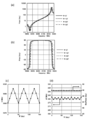
- FIG. 3A, FIG. 3B, and FIG. 3C are diagrams showing impedance characteristics, phase characteristics, and the difference between the resonance frequency and the anti-resonance frequency of the resonator according to the embodiment, respectively.
- FIG. 4A, FIG. 4B, FIG. 4C, and FIG. 4D are impedance characteristics, phase characteristics, resonance frequency, and the difference between the resonance frequency and the antiresonance frequency of the resonator according to the embodiment, respectively. It is a figure which shows and a maximum phase value.
- FIG. 5C are plan views showing arrangement examples of a plurality of resonators. It is a diagram which shows the characteristic of the resonator which concerns on a comparative example.
- FIG. 7A, FIG. 7B and FIG. 7C are diagrams corresponding to FIG. 3 when the thickness of the LN layer is different.
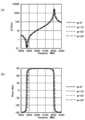
- 8A and 8B are diagrams showing impedance characteristics and phase characteristics of the resonator according to the embodiment.
- 9A and 9B are diagrams showing the impedance characteristic and the phase characteristic of the resonator according to the embodiment.
- 10A and 10B are diagrams showing the impedance characteristic and the phase characteristic of the resonator according to the embodiment. It is a circuit diagram which shows typically the structure of the duplexer as an example of utilization of the elastic wave apparatus of FIG.
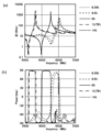
- FIG. 14A and 14B are diagrams showing impedance characteristics and phase characteristics of the acoustic wave device shown in FIG. 13, respectively.
- 15(a), 15(b), and 15(c) are diagrams showing the resonance frequency, the difference between the resonance frequency and the anti-resonance frequency, and the maximum phase value of the acoustic wave device shown in FIG. 13, respectively.
- the acoustic wave device may be either upward or downward in any direction, but hereinafter, for convenience, an orthogonal coordinate system composed of the D1 axis, the D2 axis, and the D3 axis is defined and ,
- the term “upper surface” or “lower surface” may be used with the positive side of the D3 axis as the upper side.
- the term “planar view” or “planar see-through” means viewing in the D3 axis direction unless otherwise specified.
- the D1 axis is defined to be parallel to the propagation direction of elastic waves propagating along the upper surface of the LN layer described later, and the D2 axis is defined to be parallel to the upper surface of the LN layer and orthogonal to the D1 axis.
- the D3 axis is defined to be orthogonal to the upper surface of the LN layer.
- FIG. 1 is a plan view showing a configuration of a main part of the acoustic wave device 1.
- FIG. 2 is a sectional view taken along line II-II in FIG.
- the acoustic wave device 1 is located, for example, on the substrate 3 (FIG. 2), the multilayer film 5 (FIG. 2) located on the substrate 3, the LN layer 7 located on the multilayer film 5, and the LN layer 7. And a conductive layer 9.
- Each layer has, for example, a substantially constant thickness.
- the combination of the substrate 3, the multilayer film 5 and the LN layer 7 may be referred to as the fixed substrate 2 (FIG. 2).
- the acoustic wave device 1 when a voltage is applied to the conductive layer 9, the acoustic wave propagating in the LN layer 7 is excited.
- the elastic wave device 1 constitutes, for example, a resonator and/or a filter that uses this elastic wave.
- the multilayer film 5 contributes to, for example, reflecting elastic waves and confining the energy of the elastic waves in the LN layer 7.
- the substrate 3 contributes to reinforcing the strength of the multilayer film 5 and the LN layer 7, for example.
- the substrate 3 does not directly affect the electrical characteristics of the acoustic wave device 1, as will be understood from the description below. Therefore, the material and size of the substrate 3 may be set appropriately.
- the material of the substrate 3 is, for example, an insulating material, and the insulating material is, for example, resin or ceramic.
- the substrate 3 may be made of a material having a lower coefficient of thermal expansion than the LN layer 7 or the like. In this case, for example, it is possible to reduce the risk that the frequency characteristics of the acoustic wave device 1 will change due to temperature changes. Examples of such a material include a semiconductor such as silicon, a single crystal such as sapphire, and a ceramic such as an aluminum oxide sintered body.
- the substrate 3 may be configured by stacking a plurality of layers made of different materials. The thickness of the substrate 3 is thicker than that of the LN layer 7, for example.
- the multilayer film 5 includes a low sound velocity layer 11 made of a material having a lower sound velocity than the LN layer 7 such as silicon dioxide (SiO 2 ), and tantalum pentoxide (Ta 2 O 5 ), hafnium oxide (HfO 3 ), or the like.
- the LN layer 7 and the high sonic layer 13 made of a material having a higher sonic velocity are alternately laminated.
- the high sound velocity layer 13 has a higher acoustic impedance than the low sound velocity layer 11.
- the elastic wave reflectance is relatively high at the interface between the two.
- leakage of elastic waves propagating through the LN layer 7 is reduced.
- the number of laminated layers of the multilayer film 5 may be set appropriately.
- the total number of laminated layers of the low sound velocity layer 11 and the high sound velocity layer 13 may be 3 or more and 12 or less.
- the multilayer film 5 may be composed of a total of two layers, one low sound velocity layer 11 and one high sound velocity layer 13.
- the total number of laminated layers of the multilayer film 5 may be even or odd, but the layer in contact with the LN layer 7 is the low acoustic velocity layer 11.
- the layer in contact with the substrate 3 may be the low sound velocity layer 11 or the high sound velocity layer 13.
- an additional layer may be inserted between each layer for the purpose of adhesion and prevention of diffusion. In that case, there is no problem if the layer is thin enough not to affect the characteristics (approximately 0.01 ⁇ or less based on the wavelength ⁇ described later).
- the LN layer 7 is composed of a single crystal of lithium niobate (LiNbO 3 , LN).
- the cut angle of the LN layer 7 is, for example, Euler angles ( ⁇ , ⁇ , ⁇ ) (0° ⁇ 10°, ⁇ 25° or more and 15° or less, 0° or more and 360° or less).
- the thickness of the LN layer 7 is relatively thin, and is, for example, 0.3 ⁇ or less with respect to ⁇ .
- the conductive layer 9 is made of metal, for example.
- the metal may be of any suitable type, for example, aluminum (Al) or an alloy containing Al as a main component (Al alloy).
- the Al alloy is, for example, an aluminum-copper (Cu) alloy.
- the conductive layer 9 may be composed of a plurality of metal layers. For example, a relatively thin layer made of titanium (Ti) may be provided between Al or Al alloy and the LN layer 7 to enhance their bondability.
- the conductive layer 9 is formed so as to constitute the resonator 15 in the example of FIG.
- the resonator 15 is configured as a so-called 1-port elastic wave resonator, and when an electric signal of a predetermined frequency is input from one of the terminals 17A and 17B which are conceptually and schematically shown, resonance is caused and the resonance is generated. The generated signal can be output from the other terminal 17A and 17B.
- the conductive layer 9 (resonator 15) includes, for example, an IDT electrode 19 and a pair of reflectors 21 located on both sides of the IDT electrode 19.
- the IDT electrode 19 includes a pair of comb-teeth electrodes 23. Note that one comb-tooth electrode 23 is hatched to improve visibility. Each comb-tooth electrode 23 includes, for example, a bus bar 25, a plurality of electrode fingers 27 extending from the bus bar 25 in parallel with each other, and a dummy electrode 29 protruding from the bus bar 25 between the plurality of electrode fingers 27. The pair of comb-teeth electrodes 23 are arranged so that the plurality of electrode fingers 27 are engaged with each other (intersecting).
- the bus bar 25 is, for example, formed in a long shape having a substantially constant width and linearly extending in the propagation direction of the elastic wave (the direction in which the electrode fingers 27 are repeatedly arranged, in this example, the D1 axis direction).
- the pair of bus bars 25 are opposed to each other in the direction (D2 axis direction) orthogonal to the elastic wave propagation direction.
- the bus bar 25 may have a changed width or may be inclined with respect to the propagation direction of the elastic wave.
- Each electrode finger 27 is, for example, formed in an elongated shape having a substantially constant width and extending linearly in a direction (D2 axis direction) orthogonal to the elastic wave propagation direction.
- the plurality of electrode fingers 27 are arranged in the elastic wave propagation direction. Further, the plurality of electrode fingers 27 of the one comb-teeth electrode 23 and the plurality of electrode fingers 27 of the other comb-teeth electrode 23 are basically arranged alternately.
- the pitch p of the plurality of electrode fingers 27 (for example, the distance between the centers of two electrode fingers 27 adjacent to each other) is basically constant in the IDT electrode 19. It should be noted that a part of the IDT electrode 19 may be provided with a narrow pitch part in which the pitch p is narrower than the other part, or a wide pitch part in which the pitch p is wider than the other part.
- the pitch p is the pitch of the portion (most of the plurality of electrode fingers 27) excluding the peculiar portion such as the narrow pitch portion or the wide pitch portion as described above unless otherwise specified. Shall be said. Also, in the case where the pitches of most of the plurality of electrode fingers 27 except for the peculiar portion are changed, the average value of the pitches of most of the plurality of electrode fingers 27 is set as the value of pitch p. May be used. Therefore, a value twice the pitch p is set as the wavelength ⁇ .
- the number of electrode fingers 27 may be appropriately set according to the electrical characteristics required of the resonator 15. Since FIG. 2 is a schematic diagram, the number of electrode fingers 27 is shown small. The same applies to the strip electrode 33 of the reflector 21 described later.
- the lengths and widths of the plurality of electrode fingers 27 may be appropriately set according to required electrical characteristics and the like.
- the dummy electrode 29 has, for example, a substantially constant width and projects in a direction orthogonal to the propagation direction of the elastic wave.
- the plurality of dummy electrodes 29 are arranged at the same pitch as the plurality of electrode fingers 27, and the tip of the dummy electrode 29 of the one comb-teeth electrode 23 is separated from the tip of the electrode finger 27 of the other comb-teeth electrode 23 by a gap. Are facing through.
- the IDT electrode 19 may not include the dummy electrode 29.
- the pair of reflectors 21 are located on both sides of the plurality of IDT electrodes 19 in the acoustic wave propagation direction.
- the reflector 21 includes a pair of bus bars 31 facing each other and a plurality of strip electrodes 33 extending between the pair of bus bars 31.
- the upper surface of the LN layer 7 may be covered with a protective film made of SiO 2 , Si 3 N 4 or the like from above the conductive layer 9.
- the protective film may be a laminate of a plurality of layers made of these materials. The protective film may simply prevent corrosion of the conductive layer 9 or may contribute to temperature compensation.
- an additional film made of an insulator or a metal may be provided on the upper surface or the lower surface of the IDT electrode 19 and the reflector 21 in order to improve the reflection coefficient of elastic waves.
- the configurations shown in FIGS. 1 and 2 may be packaged appropriately.
- the package may be, for example, one in which the configuration shown in the figure is mounted on a substrate (not shown) such that the upper surfaces of the LN layers 7 face each other with a gap therebetween, and resin sealing is performed from above. It may be a wafer level package type in which a box-shaped cover is provided on the top.
- the LN layer 7 is relatively thin, and its Euler angles ( ⁇ , ⁇ , ⁇ ) are (0° ⁇ 10°, ⁇ 25° to 15°, 0° to 360°).
- Modal elastic waves are available.
- the propagation velocity (sound velocity) of the elastic wave in the slab mode is higher than the propagation velocity of a general SAW (Surface Acoustic Wave).
- the propagation speed of a general SAW is 3000 to 4000 m/s, while the propagation speed of elastic waves in the slab mode is 10000 m/s or more. Therefore, it is possible to realize resonance in a high frequency region as compared with the related art with the pitch p equal to that of the related art.
- a resonance frequency (fr) of 5 GHz or higher can be realized with a pitch p of 1 ⁇ m or higher.
- the inventor of the present application variously changes the material and thickness of the multilayer film 5, the Euler angle of the piezoelectric layer (LN layer 7 in the present embodiment), the material and thickness, and the thickness of the conductive layer 9 to obtain the elastic wave.
- a simulation calculation was performed on the frequency characteristics of the device 1. Then, the inventors have found conditions that can realize resonance in a relatively high frequency region (for example, 5 GHz or more) by using elastic waves in the slab mode. Specifically, it is as follows.
- the Euler angle of the LN layer 7 is swung to perform a simulation, and resonance in a relatively high high frequency region can be realized, and the Euler angle of the LN layer 7 where spurious does not exist near fr and the anti-resonance frequency (fa) is obtained.
- the LN layer 7 has a thickness of 0.1875 ⁇
- the low sound velocity layer 11 has a thickness of 0.09 ⁇
- the high sound velocity layer 13 has a thickness of 0.07 ⁇
- the conductive layer 9 has a thickness of 0.06 ⁇
- the pitch p is 1 ⁇ m
- Duty0 It is set to 0.5.
- FIGS. 3(a) to 3(c) 3A is an impedance characteristic
- FIG. 3B is a phase characteristic
- FIG. 3C is a diagram showing how the difference ( ⁇ f) between fr and fa changes when ⁇ is changed. is there.
- the horizontal axis represents frequency
- the vertical axis represents absolute value of impedance in FIG. 3A
- FIG. 3B represents phase
- the horizontal axis represents ⁇ and the vertical axis represents ⁇ f.
- FIG. 4(a) shows impedance characteristics
- FIG. 4(b) shows phase characteristics
- FIG. 4(c) shows fr
- FIG. 4(d) shows ⁇ f and the maximum phase value (MaxPhase) between fr and fa. Is shown.
- a plurality of resonators 15 shown in FIG. 1 may be provided and the propagation angles (directions of repeated arrangement of electrode fingers) may be different from each other.
- the propagation angle of the series resonator may be different from the propagation angle of the parallel resonator.
- the propagation angle of the series resonator is set to any of 15° to 45°, 75° to 105°, 135° to 165°, 195° to 225°, 255° to 285°, and 315° to 345°.
- the propagation angles of the parallel resonators are -15° (345°) to 15°, 45° to 75°, 105° to 135°, 165° to 195°, 225° to 255°, 285° to 315°. Good.
- the upper limit and the lower limit are included in the angular range of the series resonator, and the upper limit and the lower limit are not included in the angular range of the parallel resonator.
- the propagation angle of the series resonator is 20°+60° ⁇ n1 or more and 40°+60° ⁇ n1 or less, and the propagation angle of the parallel resonator is ⁇ 10°+60° ⁇ n2 or more 10°+60° ⁇ n2. It may be as follows. Hereinafter, the propagation angle may be represented by ⁇ .
- the fr can be changed by the difference in the propagation angle, which facilitates the design. For example, fr can be further moved to the higher frequency side without reducing the pitch p.
- the thickness of the LN layer 7 and the thickness of each layer of the multilayer film 5 are optimized by the pitch p of the electrode fingers 27, the pitch p of each resonator 15 is set even when there are a plurality of resonators 15 having different fr. Since they can be brought close to each other, a high-performance acoustic wave device can be provided.
- the series resonator 15S (first resonator) is arranged so that ⁇ is 90°
- the parallel resonator 15P (second resonator) is ⁇ .
- the series resonator 15S is arranged so that ⁇ is 30° and 90°
- the parallel resonator 15P is arranged so that ⁇ is 0° and 60°. Good. In this case, the degree of freedom of layout is further increased.
- the propagation angle is different between the series resonator 15S and the parallel resonator 15P, but the propagation angle may be different between the series resonators and the parallel resonators.
- fr may be made different between series resonators and parallel resonators in order to improve the shoulder characteristics of the filter and to adjust the out-of-band attenuation characteristics.
- the propagation angle may be used for this adjustment.
- Fig. 5(c) shows the case where the propagation angle ( ⁇ ) is made different between the series resonators.
- the first series resonator 15S1 (first resonator) and the second series resonator 15S2 (second resonator) may be present in the series resonator 15S.
- resonators having the same pitch and different fr can be realized. For example, it is possible to suppress a decrease in the power resistance due to the pitch becoming small and the electric power being concentrated in a specific resonator. be able to.
- adjacent resonators means that other resonators are not located between the resonators, and the directions in which they are adjacent are not limited.
- the propagation angle is made different between the resonators located on the extension line of the propagation direction, the above effect is enhanced.
- the resonator 15 is shown in a rectangular shape, and the long side indicates the propagation direction.
- the propagation direction in each resonator that is, the direction in which the electrode fingers are repeatedly arranged may be indicated by an arrow in a rectangle representing the resonator.
- Comparative Example 1 a resonator having the same configuration as that of the above-described embodiment except that a thick LN substrate was used as the LN layer 7 and the multilayer film 5 was not provided, and the characteristics were measured with different propagation angles.
- Comparative Example 2 a resonator having a configuration in which the Euler angle of the LN substrate was changed to (0, 38, ⁇ ) from Comparative Example 1 was made, and the characteristics were measured with different propagation angles.
- the Euler angle corresponds to the cut angle generally used for the LN substrate.
- Comparative Example 1-2 a resonator having a configuration in which the thickness of the LN substrate of Comparative Example 1 was 0.5 ⁇ and the Si substrate was arranged on the lower surface of the resonator was measured, and the characteristics were measured with different propagation angles.
- Comparative Example 2-2 a resonator having a configuration in which the thickness of the LN substrate of Comparative Example 2 was 0.5 ⁇ and the Si substrate was arranged on the lower surface thereof was prepared, and the characteristics were measured with different propagation angles. ..
- FIG. 6 is a diagram showing the correlation between the phase characteristics and the propagation angle and the correlation between ⁇ f and the propagation angle of Comparative Examples 1, 1-2, 2 and 2-1.
- no elastic wave in the slab mode could be confirmed, and it was confirmed that the resonance frequency was in the 2 MHz range. That is, it was confirmed that the types of elastic waves handled were different from those of the above-described embodiment.
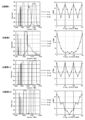
- FIG. 7 is a diagram corresponding to FIG. 3 when the thickness of the LN layer is changed.
- the thickness of the LN layer 7 may be 0.1175 ⁇ or more and 0.22 ⁇ or less. The characteristics shown in FIG. 3 are obtained by setting the thickness of the LN layer 7 to 0.1875 ⁇ .
- FIG. 8A and 8B show simulation results when the thickness of the high sonic layer 13 is set to 0.07 ⁇ and the thickness of the low sonic layer 11 is changed.
- FIG. 8A shows impedance characteristics
- FIG. 8B shows phase characteristics.
- the horizontal axis represents the frequency
- the vertical axis represents the absolute value of impedance in FIG. 8A
- the phase in FIG. 8B is shown.
- the thickness of the low sound velocity layer 11 may be 0.065 ⁇ or more and 0.1375 ⁇ or less.
- FIGS. 9A and 9B show the simulation results when the thickness of the low sonic layer 11 is set to 0.09 ⁇ and the thickness of the high sonic layer 13 is changed.
- 9A and 9B are diagrams corresponding to FIGS. 8A and 8B.
- the thickness of the high sound velocity layer 13 may be 0.055 ⁇ or more and 0.1175 ⁇ or less.
- the surface roughness of each layer constituting the multilayer film 5 may be increased as the LN layer 7 approaches the substrate 3. More specifically, the surface roughness of the layer in contact with the LN layer 7 in the low acoustic velocity layer 11 is smaller than that of the layer located closest to the substrate 3 side. With such a configuration, the bulk wave transmitted from the LN layer 3 can be scattered.
- FIGS. 10A and 10B are diagrams corresponding to FIGS. 9A and 9B, respectively.
- the conductive layer 9 may have a thickness of 0.01 ⁇ or more and 0.0875 ⁇ or less.
- the acoustic wave device 1 may be manufactured by combining various known processes.
- the low acoustic velocity layer 11 and the high acoustic velocity layer 13 are sequentially formed on the wafer to be the substrate 3 by a thin film forming method such as CVD (chemical vapor deposition).
- a wafer to be the LN layer 7 is prepared by the same manufacturing process as that for a general LN substrate wafer.
- the wafer to be the LN layer 7 is attached to the wafer to be the substrate 3 and the multilayer film 5.
- the LN layer 7 is brought into direct contact with the uppermost layer (eg, SiO 2 layer) of the multilayer film 5.
- Heat treatment or the like may be performed before or after the contact. After that, a metal layer to be the conductive layer 9 is formed and patterned on the upper surface of the wafer to be the LN layer 7, and the wafer is diced. Thereby, the acoustic wave device 1 is manufactured. Of course, appropriate steps may be added depending on the form of the package.
- an acoustic wave device 1A that does not include a multilayer film may be used.
- the acoustic wave device 1A is similar to the acoustic wave device 1 in that the LN layer 7 is supported by the substrate 3, but there is no multilayer film 5 and the region where the IDT electrode 19 is located in the LN layer 7 and the substrate 3 are separated. It has a membrane shape with voids in between. This void allows the elastic wave to be confined in the LN layer 7.
- a concave portion 3 a is formed on the upper surface of the substrate 3.
- the LN layer 7 is directly or indirectly bonded to the substrate 3 so that the recess 3a and the IDT electrode 19 overlap each other in a top view.
- the basic configuration of the acoustic wave device 1A is that the Euler angle of the LN layer 7 is (0, 0, ⁇ ), the thickness of the LN layer 7 is 0.185 ⁇ , the thickness of the conductive layer 9 is 0.065 ⁇ , the pitch p is 1 ⁇ m, and Duty0. It is set to 0.5.
- FIGS. 15A, 15B, and 15C show fr, ⁇ f, and maximum phase value when ⁇ is changed.
- the dyne back wave device 1A like the elastic wave device 1, does not change fr, ⁇ f, and maximum phase value even when ⁇ (propagation angle) is changed. It was confirmed that there was little fluctuation.
- the example shown in FIG. 13 has a configuration in which the substrate 3 is provided with a recess, but the configuration is not limited to this.
- a convex portion functioning as a spacer may be provided on the upper surface of the substrate 3 having a flat upper surface, and the LN layer may be arranged on the convex portion.
- the convex portion may be formed of a material different from that of the substrate 3.
- the recess 3a may be provided with one recess 3a for one resonator, or may be provided with a recess 3a for withstanding a plurality of resonators.
- the material of the substrate 3 is not particularly limited, but a Si substrate may be used in consideration of workability.
- FIG. 11 is a circuit diagram schematically showing the configuration of the duplexer 101 as an example of using the elastic wave device 1.
- the comb-teeth electrode 23 is schematically shown in this figure by a forked shape of a fork, and the reflector 21 is a single line bent at both ends. It is represented by.
- the demultiplexer 101 filters, for example, a transmission signal from the transmission terminal 105 and outputs it to the antenna terminal 103, and a reception signal from the antenna terminal 103 and outputs it to a pair of reception terminals 107. It has a reception filter 111.
- the transmission filter 109 is composed of, for example, a ladder type filter in which a plurality of resonators 15 are connected in a ladder type. That is, the transmission filter 109 connects a plurality (or one) of the resonators 15 connected in series between the transmission terminal 105 and the antenna terminal 103, the series line (series arm) thereof, and the reference potential. A plurality of (even one is possible) resonators 15 (parallel arms). The plurality of resonators 15 that form the transmission filter 109 are provided, for example, on the same fixed substrate 2 (3, 5, and 7).
- the reception filter 111 includes, for example, a resonator 15 and a multimode type filter (including a double mode type filter) 113.
- the multimode filter 113 has a plurality of (three in the illustrated example) IDT electrodes 19 arranged in the propagation direction of the elastic wave, and a pair of reflectors 21 arranged on both sides thereof.
- the resonator 15 and the multimode filter 113 that form the reception filter 111 are provided on the same fixed substrate 2, for example.
- the transmission filter 109 and the reception filter 111 may be provided on the same fixed substrate 2 or different fixed substrates 2.
- FIG. 11 is merely an example of the configuration of the demultiplexer 101, and the reception filter 111 may be configured by a ladder type filter like the transmission filter 109, for example.
- the demultiplexer 101 includes the transmission filter 109 and the reception filter 111 has been described, but the demultiplexer 101 is not limited to this. For example, it may be a diplexer or a multiplexer including three or more filters.
- FIG. 12 is a block diagram showing a main part of a communication device 151 as an example of using the elastic wave device 1 (branching filter 101).
- the communication device 151 performs wireless communication using radio waves and includes the duplexer 101.
- the transmission information signal TIS including the information to be transmitted is modulated by the RF-IC (Radio Frequency Integrated Circuit) 153 and the frequency is raised (conversion of the carrier frequency to a high frequency signal) to form a transmission signal TS.
- the transmission signal TS has unnecessary components other than the transmission pass band removed by the band pass filter 155, is amplified by the amplifier 157, and is input to the demultiplexer 101 (transmission terminal 105). Then, the demultiplexer 101 (transmission filter 109) removes unnecessary components other than the transmission pass band from the input transmission signal TS, and outputs the removed transmission signal TS from the antenna terminal 103 to the antenna 159. ..
- the antenna 159 converts the input electric signal (transmission signal TS) into a radio signal (radio wave) and transmits it.
- a radio signal (radio wave) received by the antenna 159 is converted into an electric signal (received signal RS) by the antenna 159 and input to the duplexer 101 (antenna terminal 103).
- the demultiplexer 101 removes unnecessary components other than the reception pass band from the input reception signal RS and outputs it from the reception terminal 107 to the amplifier 161.
- the output reception signal RS is amplified by the amplifier 161, and unnecessary components other than the reception pass band are removed by the band pass filter 163. Then, the reception signal RS is subjected to frequency reduction and demodulation by the RF-IC 153 to be a reception information signal RIS.
- the transmission information signal TIS and the reception information signal RIS may be low-frequency signals (baseband signals) containing appropriate information, and are, for example, analog voice signals or digitized voice signals.
- the pass band of the radio signal may be set appropriately, and in the present embodiment, a pass band of relatively high frequency (for example, 5 GHz or more) is also possible.
- the modulation method may be phase modulation, amplitude modulation, frequency modulation, or a combination of two or more of these.
- the direct conversion method is illustrated in FIG. 12 as the circuit method, any other suitable circuit method may be used, and for example, a double superheterodyne method may be used.
- FIG. 12 schematically shows only a main part, and a low-pass filter, an isolator or the like may be added at an appropriate position, or a position of an amplifier or the like may be changed.
- the present invention is not limited to the above embodiment and may be implemented in various modes.
- the thickness of each layer and the Euler angle of the LN layer may be values outside the range exemplified in the embodiment.
Abstract
[Problem] To provide an elastic wave device capable of achieving resonance at a frequency that is relatively high with respect to the pitch of electrode fingers. [Solution] An elastic wave device 1 comprising: a substrate 3; a multilayer film 5 positioned on the substrate 3; an LT layer 7 formed from a single crystal of LiTaO3 and positioned on the multilayer film 5; and an IDT electrode 19 positioned on the LT layer 7. When a value equivalent to two times the pitch P of the electrode fingers 27 of the IDT electrode 19 is denoted by λ, the thickness of the LT layer 7 is 0.3λ or less. The Euler angles of the LT layer 7 are (0° ± 10°, -25° to 15° inclusive, and 0° to 360° inclusive).
Description
本開示は、弾性波を利用する弾性波装置、当該弾性波装置を含む分波器および通信装置に関する。
The present disclosure relates to an elastic wave device that uses elastic waves, a duplexer including the elastic wave device, and a communication device.
圧電体上のIDT(InterDigital Transducer)電極に電圧を印加して、圧電体を伝搬する弾性波を生じさせる弾性波装置が知られている。IDT電極は、1対の櫛歯電極を有している。1対の櫛歯電極は、それぞれ複数の電極指(櫛の歯に相当する)を有しており、互いに噛み合うように配置される。弾性波装置においては、電極指のピッチの2倍を波長とする弾性波の定在波が形成され、この定在波の周波数が共振周波数となる。従って、弾性波装置の共振点は、電極指のピッチによって規定される。
An elastic wave device is known that applies a voltage to an IDT (Inter Digital Transducer) electrode on a piezoelectric body to generate an elastic wave propagating through the piezoelectric body. The IDT electrode has a pair of comb-teeth electrodes. Each of the pair of comb-teeth electrodes has a plurality of electrode fingers (corresponding to the teeth of the comb) and is arranged so as to mesh with each other. In the elastic wave device, a standing wave of an elastic wave having a wavelength that is twice the pitch of the electrode fingers is formed, and the frequency of this standing wave becomes the resonance frequency. Therefore, the resonance point of the acoustic wave device is defined by the pitch of the electrode fingers.
近年、弾性波装置として、基板と、基板上に位置している音響反射層と、音響反射層上に位置している圧電体層と、圧電体層上に位置しているIDT電極とを有するものが提案されている。音響反射層は、低音響インピーダンス層と高音響インピーダンス層とを交互に積層して構成されている。このような構成により、弾性波として板波を利用でき、5GHzに共振を有する3μm程度の電極指の周期で実現できる。
In recent years, an elastic wave device has a substrate, an acoustic reflection layer located on the substrate, a piezoelectric layer located on the acoustic reflection layer, and an IDT electrode located on the piezoelectric layer. Things have been proposed. The acoustic reflection layer is configured by alternately stacking low acoustic impedance layers and high acoustic impedance layers. With such a configuration, a plate wave can be used as an elastic wave, and it can be realized with a period of about 3 μm of electrode fingers having resonance at 5 GHz.
電極指のピッチに対して相対的に周波数が高い共振を実現できる弾性波装置、分波器および通信装置が提供されることが望まれる。
It is desirable to provide an acoustic wave device, a duplexer, and a communication device that can realize resonance having a relatively high frequency with respect to the pitch of the electrode fingers.
本開示の一態様に係る弾性波装置は、LiNbO3の単結晶により構成されているLN層と、前記LN層上に位置しているIDT電極と、を有している。前記LN層の厚さが、前記IDT電極の電極指のピッチの2倍をλとしたときに、0.3λ以下であり、前記LT層のオイラー角(φ,θ,ψ)が、(0°±10°,-25°以上15°以下,0°以上360°以下)である。
An acoustic wave device according to an aspect of the present disclosure includes an LN layer made of a single crystal of LiNbO 3 and an IDT electrode located on the LN layer. The thickness of the LN layer is 0.3λ or less, where λ is twice the pitch of the electrode fingers of the IDT electrode, and the Euler angle (φ, θ, ψ) of the LT layer is (0 °±10°, -25° or more and 15° or less, 0° or more and 360° or less).
本開示の一態様に係る分波器は、アンテナ端子と、前記アンテナ端子へ出力される信号をフィルタリングする送信フィルタと、前記アンテナ端子から入力される信号をフィルタリングする受信フィルタと、を有しており、前記送信フィルタおよび前記受信フィルタの少なくとも一方が上記の弾性波装置を含んでいる。
A duplexer according to an aspect of the present disclosure includes an antenna terminal, a transmission filter that filters a signal output to the antenna terminal, and a reception filter that filters a signal input from the antenna terminal. At least one of the transmission filter and the reception filter includes the acoustic wave device.
本開示の一態様に係る通信装置は、アンテナと、前記アンテナに前記アンテナ端子が接続されている上記の分波器と、前記送信フィルタおよび前記受信フィルタに対して信号経路に関して前記アンテナ端子とは反対側に接続されているICと、を有している。
A communication device according to an aspect of the present disclosure includes an antenna, the above-mentioned duplexer in which the antenna terminal is connected to the antenna, and the antenna terminal with respect to a signal path with respect to the transmission filter and the reception filter. And an IC connected to the opposite side.
上記の構成によれば、電極指のピッチに対して相対的に周波数が高い共振を実現できる。
With the above configuration, it is possible to realize resonance having a relatively high frequency with respect to the pitch of the electrode fingers.
以下、本開示に係る実施形態について、図面を参照して説明する。なお、以下の説明で用いられる図は模式的なものであり、図面上の寸法比率等は現実のものとは必ずしも一致していない。
Hereinafter, embodiments according to the present disclosure will be described with reference to the drawings. Note that the drawings used in the following description are schematic, and the dimensional ratios and the like in the drawings do not always match the actual ones.
本開示に係る弾性波装置は、いずれの方向が上方または下方とされてもよいものであるが、以下では、便宜的に、D1軸、D2軸およびD3軸からなる直交座標系を定義するとともに、D3軸の正側を上方として、上面または下面等の用語を用いることがある。また、平面視または平面透視という場合、特に断りがない限りは、D3軸方向に見ることをいう。なお、D1軸は、後述するLN層の上面に沿って伝搬する弾性波の伝搬方向に平行になるように定義され、D2軸は、LN層の上面に平行かつD1軸に直交するように定義され、D3軸は、LN層の上面に直交するように定義されている。
The acoustic wave device according to the present disclosure may be either upward or downward in any direction, but hereinafter, for convenience, an orthogonal coordinate system composed of the D1 axis, the D2 axis, and the D3 axis is defined and , The term "upper surface" or "lower surface" may be used with the positive side of the D3 axis as the upper side. Further, the term "planar view" or "planar see-through" means viewing in the D3 axis direction unless otherwise specified. The D1 axis is defined to be parallel to the propagation direction of elastic waves propagating along the upper surface of the LN layer described later, and the D2 axis is defined to be parallel to the upper surface of the LN layer and orthogonal to the D1 axis. The D3 axis is defined to be orthogonal to the upper surface of the LN layer.
(弾性波装置の全体構成)
図1は、弾性波装置1の要部の構成を示す平面図である。図2は、図1のII-II線における断面図である。 (Overall structure of elastic wave device)
FIG. 1 is a plan view showing a configuration of a main part of theacoustic wave device 1. FIG. 2 is a sectional view taken along line II-II in FIG.
図1は、弾性波装置1の要部の構成を示す平面図である。図2は、図1のII-II線における断面図である。 (Overall structure of elastic wave device)
FIG. 1 is a plan view showing a configuration of a main part of the
弾性波装置1は、例えば、基板3(図2)と、基板3上に位置する多層膜5(図2)と、多層膜5上に位置するLN層7と、LN層7上に位置する導電層9とを有している。各層は、例えば、概ね一定の厚さとされている。なお、基板3、多層膜5およびLN層7の組み合わせを固着基板2(図2)ということがある。
The acoustic wave device 1 is located, for example, on the substrate 3 (FIG. 2), the multilayer film 5 (FIG. 2) located on the substrate 3, the LN layer 7 located on the multilayer film 5, and the LN layer 7. And a conductive layer 9. Each layer has, for example, a substantially constant thickness. The combination of the substrate 3, the multilayer film 5 and the LN layer 7 may be referred to as the fixed substrate 2 (FIG. 2).
弾性波装置1では、導電層9に電圧が印加されることによって、LN層7を伝搬する弾性波が励振される。弾性波装置1は、例えば、この弾性波を利用する共振子および/またはフィルタを構成している。多層膜5は、例えば、弾性波を反射して弾性波のエネルギーをLN層7に閉じ込めることに寄与している。基板3は、例えば、多層膜5およびLN層7の強度を補強することに寄与している。
In the acoustic wave device 1, when a voltage is applied to the conductive layer 9, the acoustic wave propagating in the LN layer 7 is excited. The elastic wave device 1 constitutes, for example, a resonator and/or a filter that uses this elastic wave. The multilayer film 5 contributes to, for example, reflecting elastic waves and confining the energy of the elastic waves in the LN layer 7. The substrate 3 contributes to reinforcing the strength of the multilayer film 5 and the LN layer 7, for example.
(固着基板の概略構成)
基板3は、後述する説明から理解されるように、直接的には、弾性波装置1の電気的特性に影響しない。従って、基板3の材料および寸法は適宜に設定されてよい。基板3の材料は、例えば、絶縁材料であり、絶縁材料は、例えば、樹脂またはセラミックである。なお、基板3は、LN層7等に比較して熱膨張係数が低い材料によって構成されていてもよい。この場合、例えば、温度変化によって弾性波装置1の周波数特性が変化してしまうおそれを低減することができる。このような材料としては、例えば、シリコン等の半導体、サファイア等の単結晶および酸化アルミニウム質焼結体等のセラミックを挙げることができる。なお、基板3は、互いに異なる材料からなる複数の層が積層されて構成されていてもよい。基板3の厚さは、例えば、LN層7よりも厚い。 (Schematic structure of fixed substrate)
Thesubstrate 3 does not directly affect the electrical characteristics of the acoustic wave device 1, as will be understood from the description below. Therefore, the material and size of the substrate 3 may be set appropriately. The material of the substrate 3 is, for example, an insulating material, and the insulating material is, for example, resin or ceramic. The substrate 3 may be made of a material having a lower coefficient of thermal expansion than the LN layer 7 or the like. In this case, for example, it is possible to reduce the risk that the frequency characteristics of the acoustic wave device 1 will change due to temperature changes. Examples of such a material include a semiconductor such as silicon, a single crystal such as sapphire, and a ceramic such as an aluminum oxide sintered body. The substrate 3 may be configured by stacking a plurality of layers made of different materials. The thickness of the substrate 3 is thicker than that of the LN layer 7, for example.
基板3は、後述する説明から理解されるように、直接的には、弾性波装置1の電気的特性に影響しない。従って、基板3の材料および寸法は適宜に設定されてよい。基板3の材料は、例えば、絶縁材料であり、絶縁材料は、例えば、樹脂またはセラミックである。なお、基板3は、LN層7等に比較して熱膨張係数が低い材料によって構成されていてもよい。この場合、例えば、温度変化によって弾性波装置1の周波数特性が変化してしまうおそれを低減することができる。このような材料としては、例えば、シリコン等の半導体、サファイア等の単結晶および酸化アルミニウム質焼結体等のセラミックを挙げることができる。なお、基板3は、互いに異なる材料からなる複数の層が積層されて構成されていてもよい。基板3の厚さは、例えば、LN層7よりも厚い。 (Schematic structure of fixed substrate)
The
多層膜5は、例えば二酸化ケイ素(SiO2)等のLN層7に比べ低音速の材料からなる低音速層11と、例えば五酸化タンタル(Ta2O5),酸化ハフニウム(HfO3)等のLN層7に比べ高音速の材料からなる高音速層13とを交互に積層することにより構成されている。高音速層13は、低音速層11に比較して音響インピーダンスが高い。これにより、両者の界面においては弾性波の反射率が比較的高くなっている。その結果、例えば、LN層7を伝搬する弾性波の漏れが低減される。
The multilayer film 5 includes a low sound velocity layer 11 made of a material having a lower sound velocity than the LN layer 7 such as silicon dioxide (SiO 2 ), and tantalum pentoxide (Ta 2 O 5 ), hafnium oxide (HfO 3 ), or the like. The LN layer 7 and the high sonic layer 13 made of a material having a higher sonic velocity are alternately laminated. The high sound velocity layer 13 has a higher acoustic impedance than the low sound velocity layer 11. As a result, the elastic wave reflectance is relatively high at the interface between the two. As a result, for example, leakage of elastic waves propagating through the LN layer 7 is reduced.
多層膜5の積層数は適宜に設定されてよい。例えば、多層膜5は、低音速層11および高音速層13の合計の積層数が3層以上12層以下とされてよい。ただし、多層膜5は、1層の低音速層11と1層の高音速層13との合計2層から構成されてもよい。また、多層膜5の合計の積層数は、偶数でもよいし、奇数でもよいが、LN層7に接する層は、低音速層11である。基板3に接する層については低音速層11であってもよいし、高音速層13であってもよい。また、各層の間に、密着や拡散防止を目的に付加的な層を挿入することがある。その場合、その層が特性に影響を与えない程度に薄ければ(後述する波長λを基準にすると、おおむね0.01λ以下とすれば)問題ない。
The number of laminated layers of the multilayer film 5 may be set appropriately. For example, in the multilayer film 5, the total number of laminated layers of the low sound velocity layer 11 and the high sound velocity layer 13 may be 3 or more and 12 or less. However, the multilayer film 5 may be composed of a total of two layers, one low sound velocity layer 11 and one high sound velocity layer 13. The total number of laminated layers of the multilayer film 5 may be even or odd, but the layer in contact with the LN layer 7 is the low acoustic velocity layer 11. The layer in contact with the substrate 3 may be the low sound velocity layer 11 or the high sound velocity layer 13. In addition, an additional layer may be inserted between each layer for the purpose of adhesion and prevention of diffusion. In that case, there is no problem if the layer is thin enough not to affect the characteristics (approximately 0.01λ or less based on the wavelength λ described later).
LN層7は、ニオブ酸リチウム(LiNbO3、LN)の単結晶によって構成されている。LN層7のカット角は、例えば、オイラー角(φ,θ,ψ)で(0°±10°,-25°以上15°以下,0°以上360°以下)である。またLN層7の厚さは、比較的薄くされており、例えば、λを基準として、0.3λ以下である。LN層7のカット角および厚さをこのように設定することにより、弾性波として、スラブモードに近い振動モードのものを利用することが可能になる。言い換えると、弾性波としてA1モードの板波を用いることができるので、後述のIDT電極19の電極指27の間隔が比較的広くても、高い周波数での共振を得ることができる。
The LN layer 7 is composed of a single crystal of lithium niobate (LiNbO 3 , LN). The cut angle of the LN layer 7 is, for example, Euler angles (φ, θ, ψ) (0°±10°, −25° or more and 15° or less, 0° or more and 360° or less). Further, the thickness of the LN layer 7 is relatively thin, and is, for example, 0.3λ or less with respect to λ. By setting the cut angle and the thickness of the LN layer 7 in this way, it is possible to use an elastic wave having a vibration mode close to the slab mode. In other words, since the plate wave of A1 mode can be used as the elastic wave, it is possible to obtain resonance at a high frequency even if the interval between the electrode fingers 27 of the IDT electrode 19 described later is relatively wide.
(導電層の概略構成)
導電層9は、例えば、金属により形成されている。金属は、適宜な種類のものとされてよく、例えば、アルミニウム(Al)またはAlを主成分とする合金(Al合金)である。Al合金は、例えば、アルミニウム-銅(Cu)合金である。なお、導電層9は、複数の金属層から構成されていてもよい。例えば、AlまたはAl合金と、LN層7との間に、これらの接合性を強化するためのチタン(Ti)からなる比較的薄い層が設けられていてもよい。 (Schematic structure of conductive layer)
Theconductive layer 9 is made of metal, for example. The metal may be of any suitable type, for example, aluminum (Al) or an alloy containing Al as a main component (Al alloy). The Al alloy is, for example, an aluminum-copper (Cu) alloy. The conductive layer 9 may be composed of a plurality of metal layers. For example, a relatively thin layer made of titanium (Ti) may be provided between Al or Al alloy and the LN layer 7 to enhance their bondability.
導電層9は、例えば、金属により形成されている。金属は、適宜な種類のものとされてよく、例えば、アルミニウム(Al)またはAlを主成分とする合金(Al合金)である。Al合金は、例えば、アルミニウム-銅(Cu)合金である。なお、導電層9は、複数の金属層から構成されていてもよい。例えば、AlまたはAl合金と、LN層7との間に、これらの接合性を強化するためのチタン(Ti)からなる比較的薄い層が設けられていてもよい。 (Schematic structure of conductive layer)
The
導電層9は、図1の例では、共振子15を構成するように形成されている。共振子15は、いわゆる1ポート弾性波共振子として構成されており、概念的かつ模式的に示す端子17Aおよび17Bの一方から所定の周波数の電気信号が入力されると共振を生じ、その共振を生じた信号を端子17Aおよび17Bの他方から出力可能である。
The conductive layer 9 is formed so as to constitute the resonator 15 in the example of FIG. The resonator 15 is configured as a so-called 1-port elastic wave resonator, and when an electric signal of a predetermined frequency is input from one of the terminals 17A and 17B which are conceptually and schematically shown, resonance is caused and the resonance is generated. The generated signal can be output from the other terminal 17A and 17B.
導電層9(共振子15)は、例えば、IDT電極19と、IDT電極19の両側に位置する1対の反射器21とを含んでいる。
The conductive layer 9 (resonator 15) includes, for example, an IDT electrode 19 and a pair of reflectors 21 located on both sides of the IDT electrode 19.
IDT電極19は、1対の櫛歯電極23を含んでいる。なお、視認性を良くするために、一方の櫛歯電極23にはハッチングを付している。各櫛歯電極23は、例えば、バスバー25と、バスバー25から互いに並列に延びる複数の電極指27と、複数の電極指27間においてバスバー25から突出するダミー電極29とを含んでいる。1対の櫛歯電極23は、複数の電極指27が互いに噛み合うように(交差するように)配置されている。
The IDT electrode 19 includes a pair of comb-teeth electrodes 23. Note that one comb-tooth electrode 23 is hatched to improve visibility. Each comb-tooth electrode 23 includes, for example, a bus bar 25, a plurality of electrode fingers 27 extending from the bus bar 25 in parallel with each other, and a dummy electrode 29 protruding from the bus bar 25 between the plurality of electrode fingers 27. The pair of comb-teeth electrodes 23 are arranged so that the plurality of electrode fingers 27 are engaged with each other (intersecting).
バスバー25は、例えば、概ね一定の幅で弾性波の伝搬方向(電極指27の繰り返し配列方向、この例ではD1軸方向)に直線状に延びる長尺状に形成されている。そして、一対のバスバー25は、弾性波の伝搬方向に直交する方向(D2軸方向)において互いに対向している。なお、バスバー25は、幅が変化したり、弾性波の伝搬方向に対して傾斜したりしていてもよい。
The bus bar 25 is, for example, formed in a long shape having a substantially constant width and linearly extending in the propagation direction of the elastic wave (the direction in which the electrode fingers 27 are repeatedly arranged, in this example, the D1 axis direction). The pair of bus bars 25 are opposed to each other in the direction (D2 axis direction) orthogonal to the elastic wave propagation direction. The bus bar 25 may have a changed width or may be inclined with respect to the propagation direction of the elastic wave.
各電極指27は、例えば、概ね一定の幅で弾性波の伝搬方向に直交する方向(D2軸方向)に直線状に延びる長尺状に形成されている。各櫛歯電極23において、複数の電極指27は、弾性波の伝搬方向に配列されている。また、一方の櫛歯電極23の複数の電極指27と他方の櫛歯電極23の複数の電極指27とは、基本的には交互に配列されている。
Each electrode finger 27 is, for example, formed in an elongated shape having a substantially constant width and extending linearly in a direction (D2 axis direction) orthogonal to the elastic wave propagation direction. In each comb-tooth electrode 23, the plurality of electrode fingers 27 are arranged in the elastic wave propagation direction. Further, the plurality of electrode fingers 27 of the one comb-teeth electrode 23 and the plurality of electrode fingers 27 of the other comb-teeth electrode 23 are basically arranged alternately.
複数の電極指27のピッチp(例えば互いに隣り合う2本の電極指27の中心間距離)は、IDT電極19内において基本的に一定である。なお、IDT電極19の一部に、他の大部分よりもピッチpが狭くなる狭ピッチ部、または他の大部分よりもピッチpが広くなる広ピッチ部が設けられてもよい。
The pitch p of the plurality of electrode fingers 27 (for example, the distance between the centers of two electrode fingers 27 adjacent to each other) is basically constant in the IDT electrode 19. It should be noted that a part of the IDT electrode 19 may be provided with a narrow pitch part in which the pitch p is narrower than the other part, or a wide pitch part in which the pitch p is wider than the other part.
なお、以下において、ピッチpという場合、特に断りがない限りは、上記のような狭ピッチ部または広ピッチ部のような特異な部分を除いた部分(複数の電極指27の大部分)のピッチをいうものとする。また、特異な部分を除いた大部分の複数の電極指27においても、ピッチが変化しているような場合においては、大部分の複数の電極指27のピッチの平均値をピッチpの値として用いてよい。そいて、このピッチpの2倍の値を波長λとする。
In the following description, the pitch p is the pitch of the portion (most of the plurality of electrode fingers 27) excluding the peculiar portion such as the narrow pitch portion or the wide pitch portion as described above unless otherwise specified. Shall be said. Also, in the case where the pitches of most of the plurality of electrode fingers 27 except for the peculiar portion are changed, the average value of the pitches of most of the plurality of electrode fingers 27 is set as the value of pitch p. May be used. Therefore, a value twice the pitch p is set as the wavelength λ.
電極指27の本数は、共振子15に要求される電気特性等に応じて適宜に設定されてよい。なお、図2は模式図であることから、電極指27の本数は少なく示されている。後述する反射器21のストリップ電極33についても同様である。
The number of electrode fingers 27 may be appropriately set according to the electrical characteristics required of the resonator 15. Since FIG. 2 is a schematic diagram, the number of electrode fingers 27 is shown small. The same applies to the strip electrode 33 of the reflector 21 described later.
複数の電極指27の長さおよび幅は、要求される電気特性等に応じて適宜に設定されてよい。
The lengths and widths of the plurality of electrode fingers 27 may be appropriately set according to required electrical characteristics and the like.
ダミー電極29は、例えば、概ね一定の幅で弾性波の伝搬方向に直交する方向に突出している。複数のダミー電極29は、複数の電極指27と同等のピッチで配列されており、一方の櫛歯電極23のダミー電極29の先端は、他方の櫛歯電極23の電極指27の先端とギャップを介して対向している。なお、IDT電極19は、ダミー電極29を含まないものであってもよい。
The dummy electrode 29 has, for example, a substantially constant width and projects in a direction orthogonal to the propagation direction of the elastic wave. The plurality of dummy electrodes 29 are arranged at the same pitch as the plurality of electrode fingers 27, and the tip of the dummy electrode 29 of the one comb-teeth electrode 23 is separated from the tip of the electrode finger 27 of the other comb-teeth electrode 23 by a gap. Are facing through. The IDT electrode 19 may not include the dummy electrode 29.
1対の反射器21は、弾性波の伝搬方向において複数のIDT電極19の両側に位置している。反射器21は、互いに対向する1対のバスバー31と、1対のバスバー31間において延びる複数のストリップ電極33とを含んでいる。
The pair of reflectors 21 are located on both sides of the plurality of IDT electrodes 19 in the acoustic wave propagation direction. The reflector 21 includes a pair of bus bars 31 facing each other and a plurality of strip electrodes 33 extending between the pair of bus bars 31.
なお、特に図示しないが、LN層7の上面は、導電層9の上から、SiO2やSi3N4等からなる保護膜によって覆われていてもよい。保護膜はこれらの材料からなる複数層の積層体としてもよい。保護膜は、単に導電層9の腐食を抑制するためのものであってもよいし、温度補償に寄与するものであってもよい。保護膜が設けられる場合等において、IDT電極19および反射器21の上面または下面には、弾性波の反射係数を向上させるために、絶縁体または金属からなる付加膜が設けられてもよい。
Although not particularly shown, the upper surface of the LN layer 7 may be covered with a protective film made of SiO 2 , Si 3 N 4 or the like from above the conductive layer 9. The protective film may be a laminate of a plurality of layers made of these materials. The protective film may simply prevent corrosion of the conductive layer 9 or may contribute to temperature compensation. When a protective film is provided, an additional film made of an insulator or a metal may be provided on the upper surface or the lower surface of the IDT electrode 19 and the reflector 21 in order to improve the reflection coefficient of elastic waves.
図1および図2に示した構成は、適宜にパッケージされてよい。パッケージは、例えば、不図示の基板上に隙間を介してLN層7の上面を対向させるように図示の構成を実装し、その上から樹脂封止するものであってもよいし、LN層7上に箱型のカバーを設けるウェハレベルパッケージ型のものであってもよい。
The configurations shown in FIGS. 1 and 2 may be packaged appropriately. The package may be, for example, one in which the configuration shown in the figure is mounted on a substrate (not shown) such that the upper surfaces of the LN layers 7 face each other with a gap therebetween, and resin sealing is performed from above. It may be a wafer level package type in which a box-shaped cover is provided on the top.
(スラブモードの利用)
LN層7は、比較的薄くされ、かつそのオイラー角(φ,θ,ψ)が(0°±10°,-25°~15°,0°~360°)とされていることから、スラブモードの弾性波を利用可能になっている。スラブモードの弾性波の伝搬速度(音速)は、一般的なSAW(Surface Acoustic Wave)の伝搬速度よりも速い。例えば、一般的なSAWの伝搬速度が3000~4000m/sであるのに対して、スラブモードの弾性波の伝搬速度は10000m/s以上である。従って、従来と同等のピッチpで、従来よりも高周波領域での共振を実現することができる。例えば、1μm以上のピッチpで5GHz以上の共振周波数(fr)を実現することができる。 (Use of slab mode)
TheLN layer 7 is relatively thin, and its Euler angles (φ, θ, ψ) are (0°±10°, −25° to 15°, 0° to 360°). Modal elastic waves are available. The propagation velocity (sound velocity) of the elastic wave in the slab mode is higher than the propagation velocity of a general SAW (Surface Acoustic Wave). For example, the propagation speed of a general SAW is 3000 to 4000 m/s, while the propagation speed of elastic waves in the slab mode is 10000 m/s or more. Therefore, it is possible to realize resonance in a high frequency region as compared with the related art with the pitch p equal to that of the related art. For example, a resonance frequency (fr) of 5 GHz or higher can be realized with a pitch p of 1 μm or higher.
LN層7は、比較的薄くされ、かつそのオイラー角(φ,θ,ψ)が(0°±10°,-25°~15°,0°~360°)とされていることから、スラブモードの弾性波を利用可能になっている。スラブモードの弾性波の伝搬速度(音速)は、一般的なSAW(Surface Acoustic Wave)の伝搬速度よりも速い。例えば、一般的なSAWの伝搬速度が3000~4000m/sであるのに対して、スラブモードの弾性波の伝搬速度は10000m/s以上である。従って、従来と同等のピッチpで、従来よりも高周波領域での共振を実現することができる。例えば、1μm以上のピッチpで5GHz以上の共振周波数(fr)を実現することができる。 (Use of slab mode)
The
(各層の材料および厚さの設定)
本願発明者は、多層膜5の材料および厚さ、圧電体層(本実施形態ではLN層7)のオイラー角、材料および厚さ、ならびに導電層9の厚さを種々変更して、弾性波装置1の周波数特性についてシミュレーション計算を行った。そして、スラブモードの弾性波を利用して比較的高い周波数領域(例えば5GHz以上)の共振を実現できる条件を見出した。具体的には、以下のとおりである。 (Setting of material and thickness of each layer)
The inventor of the present application variously changes the material and thickness of themultilayer film 5, the Euler angle of the piezoelectric layer (LN layer 7 in the present embodiment), the material and thickness, and the thickness of the conductive layer 9 to obtain the elastic wave. A simulation calculation was performed on the frequency characteristics of the device 1. Then, the inventors have found conditions that can realize resonance in a relatively high frequency region (for example, 5 GHz or more) by using elastic waves in the slab mode. Specifically, it is as follows.
本願発明者は、多層膜5の材料および厚さ、圧電体層(本実施形態ではLN層7)のオイラー角、材料および厚さ、ならびに導電層9の厚さを種々変更して、弾性波装置1の周波数特性についてシミュレーション計算を行った。そして、スラブモードの弾性波を利用して比較的高い周波数領域(例えば5GHz以上)の共振を実現できる条件を見出した。具体的には、以下のとおりである。 (Setting of material and thickness of each layer)
The inventor of the present application variously changes the material and thickness of the
(LN層7の伝搬角について)
まず、圧電体層(LN層7)のカット角および伝搬角を種々変更してシミュレーションを行なった。その結果、オイラー角(φ,θ,ψ)において、カット角に関するφ,θをそれぞれ0°±10°、-25°~15°とすることで、スラブモードの弾性波を利用して比較的高い周波数領域の共振を実現できることを見出した。さらに、LN層7が0.3λ以下であり、かつ、φ,θがこの範囲内にある場合には、伝搬角に関するψに制限はないことを見出した。 (About propagation angle of LN layer 7)
First, simulation was performed by changing the cut angle and the propagation angle of the piezoelectric layer (LN layer 7) variously. As a result, in Euler angles (φ, θ, ψ), by setting φ and θ related to the cut angle to 0°±10° and -25° to 15°, respectively, it is possible to relatively use elastic waves in the slab mode. It was found that resonance in the high frequency range can be realized. Further, it has been found that when theLN layer 7 is 0.3λ or less and φ and θ are within this range, there is no limitation on ψ related to the propagation angle.
まず、圧電体層(LN層7)のカット角および伝搬角を種々変更してシミュレーションを行なった。その結果、オイラー角(φ,θ,ψ)において、カット角に関するφ,θをそれぞれ0°±10°、-25°~15°とすることで、スラブモードの弾性波を利用して比較的高い周波数領域の共振を実現できることを見出した。さらに、LN層7が0.3λ以下であり、かつ、φ,θがこの範囲内にある場合には、伝搬角に関するψに制限はないことを見出した。 (About propagation angle of LN layer 7)
First, simulation was performed by changing the cut angle and the propagation angle of the piezoelectric layer (LN layer 7) variously. As a result, in Euler angles (φ, θ, ψ), by setting φ and θ related to the cut angle to 0°±10° and -25° to 15°, respectively, it is possible to relatively use elastic waves in the slab mode. It was found that resonance in the high frequency range can be realized. Further, it has been found that when the
まず、LN層7のオイラー角を振ってシミュレーションを行ない、比較的高い高周波領域での共振を実現でき、かつ、frおよび反共振周波数(fa)近傍にスプリアスが存在しないLN層7のオイラー角として(0,0,0)を見出した。なお、LN層7の厚みは0.1875λ、低音速層11の厚みを0.09λ,高音速層13の厚みを0.07λ,導電層9の厚みを0.06λ、ピッチpを1μm、Duty0.5としている。
First, the Euler angle of the LN layer 7 is swung to perform a simulation, and resonance in a relatively high high frequency region can be realized, and the Euler angle of the LN layer 7 where spurious does not exist near fr and the anti-resonance frequency (fa) is obtained. Found (0,0,0). The LN layer 7 has a thickness of 0.1875λ, the low sound velocity layer 11 has a thickness of 0.09λ, the high sound velocity layer 13 has a thickness of 0.07λ, the conductive layer 9 has a thickness of 0.06λ, the pitch p is 1 μm, and Duty0. It is set to 0.5.
次に、オイラー角(0,0,0)からφ,θを変化させた場合について検討する。その結果、φを±10°を超えて変化させると共振波形が崩れることが分かった。また、θを変化させたときの周波数特性の測定結果を、図3(a)~図3(c)に示す。図3(a)はインピーダンス特性、図3(b)は位相特性を示し、図3(c)はθを変化させたときのfrとfaとの差分(Δf)の変化の様子を示す図である。図3(a),図3(b)において横軸は周波数であり、縦軸は図3(a)がインピーダンスの絶対値であり、図3(b)は位相である。また、図3(c)において、横軸はθであり、縦軸はΔfを示している。
Next, consider the case where φ and θ are changed from the Euler angles (0,0,0). As a result, it was found that the resonance waveform collapsed when φ was changed over ±10°. Further, the measurement results of the frequency characteristics when θ is changed are shown in FIGS. 3(a) to 3(c). 3A is an impedance characteristic, FIG. 3B is a phase characteristic, and FIG. 3C is a diagram showing how the difference (Δf) between fr and fa changes when θ is changed. is there. In FIGS. 3A and 3B, the horizontal axis represents frequency, the vertical axis represents absolute value of impedance in FIG. 3A, and FIG. 3B represents phase. Further, in FIG. 3C, the horizontal axis represents θ and the vertical axis represents Δf.
図からも明らかなように、θを-25°より小さくするとLN結晶を使っているにも拘わらず、Δfがタンタル酸リチウム(LT)結晶を用いた場合と同等以下となる。また、15°より大きくすると、frとfaとの近傍にスプリアスが生じることが分かった。以上より、θを、-25°~15°とすればΔfが大きく、かつスプリアスの影響を低減した弾性波素子を得ることができる。
As is clear from the figure, when θ is smaller than -25°, Δf becomes equal to or less than when lithium tantalate (LT) crystal is used, even though LN crystal is used. Further, it was found that when the angle was larger than 15°, spurious was generated in the vicinity of fr and fa. From the above, it is possible to obtain an acoustic wave device having a large Δf and reducing the influence of spurious when θ is set to -25° to 15°.
次に、ψを変化させてシミュレーションを行なった。その結果を、図4に示す。図4(a)はインピーダンス特性を、図4(b)は位相特性を、図4(c)はfrを、図4(d)はΔfおよびfrとfaとの間の最大位相値(MaxPhase)を示している。
Next, a simulation was performed by changing ψ. The result is shown in FIG. 4(a) shows impedance characteristics, FIG. 4(b) shows phase characteristics, FIG. 4(c) shows fr, and FIG. 4(d) shows Δf and the maximum phase value (MaxPhase) between fr and fa. Is shown.
この図からも明らかなように、ψを変更してもスプリアスは発生せず、MaxPhaseも変化することがなかった。すなわち、ψによるロスの悪化は確認されなかった。なお、Δfは周期的な変動があるものの、変動の中心値は変化せず、その変動幅は5MHz未満の極めて小さい値であり、かつ、Δfの絶対値はLTに比べて十分に大きい値を維持していることが分かった。さらに、frに注目すると、60°周期で変動しており、30°+60°×n1(ただし、n1は0~5までの自然数)のときに最大値をとり、0°+60°×n2(ただし、n2は0~5までの自然数)のときに最小値をとり、その差は15MHz程度であった。
As is clear from this figure, spurious did not occur even if ψ was changed, and MaxPhase did not change. That is, the deterioration of loss due to ψ was not confirmed. Note that although Δf has periodic fluctuations, the center value of the fluctuations does not change, the fluctuation width is an extremely small value of less than 5 MHz, and the absolute value of Δf is a sufficiently large value compared to LT. It turned out to be maintained. Furthermore, focusing on fr, it fluctuates in a 60° cycle, and takes the maximum value at 30°+60°×n1 (where n1 is a natural number from 0 to 5), and 0°+60°×n2 (however, , N2 has a minimum value when n2 is a natural number from 0 to 5, and the difference is about 15 MHz.
このことから、図1に示す共振子15を複数設け、互いに伝搬角(電極指の繰り返し配列方向)を異ならせてもよい。例えば、複数の共振子15をラダー型に接続してフィルタを形成するときに、直列共振子の伝搬角を並列共振子の伝搬角とを異ならせてもよい。具体的には、直列共振子の伝搬角を15°~45°,75°~105°,135°~165°,195°~225°、255°~285°、315°~345°のいずれかとし、並列共振子の伝搬角を―15°(345°)~15°,45°~75°,105°~135°,165°~195°,225°~255°,285°~315°としてもよい。ただし、直列共振子の角度範囲では上限値下限値を含み、並列共振子の角度範囲では上限値下限値を含まないものとする。
Therefore, a plurality of resonators 15 shown in FIG. 1 may be provided and the propagation angles (directions of repeated arrangement of electrode fingers) may be different from each other. For example, when a plurality of resonators 15 are connected in a ladder type to form a filter, the propagation angle of the series resonator may be different from the propagation angle of the parallel resonator. Specifically, the propagation angle of the series resonator is set to any of 15° to 45°, 75° to 105°, 135° to 165°, 195° to 225°, 255° to 285°, and 315° to 345°. The propagation angles of the parallel resonators are -15° (345°) to 15°, 45° to 75°, 105° to 135°, 165° to 195°, 225° to 255°, 285° to 315°. Good. However, the upper limit and the lower limit are included in the angular range of the series resonator, and the upper limit and the lower limit are not included in the angular range of the parallel resonator.
より好ましくは、直列共振子の伝搬角は、20°+60°×n1以上40°+60°×n1以下とし、並列共振子の伝搬角は、-10°+60°×n2以上10°+60°×n2以下としてもよい。以下、伝搬角としてψで表示することがある。
More preferably, the propagation angle of the series resonator is 20°+60°×n1 or more and 40°+60°×n1 or less, and the propagation angle of the parallel resonator is −10°+60°×n2 or more 10°+60°×n2. It may be as follows. Hereinafter, the propagation angle may be represented by ψ.
このような構成とすることで、電極指のピッチpによるfr制御に加え、伝搬角の違いによってもfrを変化させることができるので、設計が容易となる。例えば、ピッチpを小さくしなくても、さらにfrを高周波数側に移動させることができる。また、LN層7の厚みや多層膜5の各層の厚みは電極指27のピッチpにより最適化されるが、frの異なる共振子15が複数存在する場合にも各共振子15のピッチpを近付けることができるので、高性能な弾性波装置を提供することができる。
With such a configuration, in addition to the fr control by the pitch p of the electrode fingers, the fr can be changed by the difference in the propagation angle, which facilitates the design. For example, fr can be further moved to the higher frequency side without reducing the pitch p. Although the thickness of the LN layer 7 and the thickness of each layer of the multilayer film 5 are optimized by the pitch p of the electrode fingers 27, the pitch p of each resonator 15 is set even when there are a plurality of resonators 15 having different fr. Since they can be brought close to each other, a high-performance acoustic wave device can be provided.
具体的には、図5(a)に示すように、直列共振子15S(第1共振子)はψが90°となるように配置し、並列共振子15P(第2共振子)はψが0°となるように配置してもよい。すなわち、直列共振子15Sと並列共振子15Pとは90°向きが異なる。この場合には、フィルタを構成する複数の共振子15のレイアウトの自由度を高めることができる。
Specifically, as shown in FIG. 5A, the series resonator 15S (first resonator) is arranged so that ψ is 90°, and the parallel resonator 15P (second resonator) is ψ. You may arrange|position so that it may become 0 degree. That is, the series resonator 15S and the parallel resonator 15P have different 90° directions. In this case, it is possible to increase the degree of freedom in layout of the plurality of resonators 15 that form the filter.
さらに、図5(b)に示すように、直列共振子15Sはψが30°,90°となるように配置し、並列共振子15Pはψが0°,60°となるように配置してもよい。この場合にはさらにレイアウトの自由度が高まる。
Further, as shown in FIG. 5B, the series resonator 15S is arranged so that ψ is 30° and 90°, and the parallel resonator 15P is arranged so that ψ is 0° and 60°. Good. In this case, the degree of freedom of layout is further increased.
また、上述の例では、直列共振子15Sと並列共振子15Pとで伝搬角を異ならせたが、直列共振子間,並列共振子間で伝搬角を異ならせてもよい。ラダー型フィルタにおいて、フィルタの肩特性を向上させるためや、帯域外減衰特性を調整するために、直列共振子間、並列共振子間でfrを異ならせることがある。この調整に伝搬角を利用してもよい。
Also, in the above example, the propagation angle is different between the series resonator 15S and the parallel resonator 15P, but the propagation angle may be different between the series resonators and the parallel resonators. In a ladder type filter, fr may be made different between series resonators and parallel resonators in order to improve the shoulder characteristics of the filter and to adjust the out-of-band attenuation characteristics. The propagation angle may be used for this adjustment.
図5(c)に直列共振子間で伝搬角(ψ)を異ならせた場合を示す。直列共振子15Sの中に第1直列共振子15S1(第1共振子)、第2直列共振子15S2(第2共振子)が存在するようにしてもよい。このような構成とすることで同一のピッチで異なるfrを有する共振子を実現できるので、例えば、特定の共振子でピッチが小さくなり電力が集中することで耐電力性が低下することを抑制することができる。
Fig. 5(c) shows the case where the propagation angle (ψ) is made different between the series resonators. The first series resonator 15S1 (first resonator) and the second series resonator 15S2 (second resonator) may be present in the series resonator 15S. With such a configuration, resonators having the same pitch and different fr can be realized. For example, it is possible to suppress a decrease in the power resistance due to the pitch becoming small and the electric power being concentrated in a specific resonator. be able to.
また、図5(a)~図5(c)に示すように、隣り合う共振子間で伝搬角が異なるように配置する場合には、共振子から漏洩する弾性波が分散され、その結果、一方が他方の共振子のスプリアス特性を悪化させることを低減することができる。ここで、隣り合う共振子とは、互いの共振子の間に他の共振子が位置しないことをいい、隣り合う方向は限定されない。ただし、伝搬方向の延長線上に位置する共振子同士で伝搬角を異ならせる場合には、上述の効果が強まる。
Further, as shown in FIGS. 5(a) to 5(c), when the resonators are arranged so that the propagation angles of adjacent resonators are different, elastic waves leaking from the resonators are dispersed, and as a result, It is possible to reduce the deterioration of the spurious characteristics of one resonator by the other resonator. Here, the term “adjacent resonators” means that other resonators are not located between the resonators, and the directions in which they are adjacent are not limited. However, when the propagation angle is made different between the resonators located on the extension line of the propagation direction, the above effect is enhanced.
なお、図5において、共振子15を矩形状で示しており、長辺側が伝搬方向を示すものとする。参考までに、図5中において、各共振子における伝搬方向、すなわち、電極指の繰り返し配列方向を、共振子を表す矩形中に矢印で示すことがある。
Note that, in FIG. 5, the resonator 15 is shown in a rectangular shape, and the long side indicates the propagation direction. For reference, in FIG. 5, the propagation direction in each resonator, that is, the direction in which the electrode fingers are repeatedly arranged may be indicated by an arrow in a rectangle representing the resonator.
なお、上述のような伝搬角を変化させてもMaxphase、Δf、スプリアス等の特性変化がないという特性は、LN層7を用い、かつその厚みが0.3λ以下であるときに初めて発現するものである。以下、上述の条件を満たさない場合の伝搬角の影響について検証した結果を示す。
The characteristic that there is no change in characteristics such as Maxphase, Δf, and spurious even if the propagation angle is changed as described above is first exhibited when the LN layer 7 is used and the thickness thereof is 0.3λ or less. Is. The results of verification of the effect of the propagation angle when the above conditions are not satisfied are shown below.
比較例1として、LN層7として厚いLN基板を用い、かつ多層膜5を備えない構成以外は上記実施形態と同等の構成の共振子を作り、伝搬角を異ならせてその特性を測定した。
As Comparative Example 1, a resonator having the same configuration as that of the above-described embodiment except that a thick LN substrate was used as the LN layer 7 and the multilayer film 5 was not provided, and the characteristics were measured with different propagation angles.
また、比較例2として、比較例1からLN基板のオイラー角を(0,38,ψ)に変更した構成の共振子を作り、伝搬角を異ならせてその特性を測定した。なお、このオイラー角はLN基板で一般的に用いられるカット角に相当する。
Also, as Comparative Example 2, a resonator having a configuration in which the Euler angle of the LN substrate was changed to (0, 38, ψ) from Comparative Example 1 was made, and the characteristics were measured with different propagation angles. The Euler angle corresponds to the cut angle generally used for the LN substrate.
さらに、比較例1-2として、比較例1のLN基板の厚みを0.5λとし、その下面にSi基板を配置した構成の共振子を作り、伝搬角を異ならせてその特性を測定した。
Further, as Comparative Example 1-2, a resonator having a configuration in which the thickness of the LN substrate of Comparative Example 1 was 0.5λ and the Si substrate was arranged on the lower surface of the resonator was measured, and the characteristics were measured with different propagation angles.
同様に、比較例2-2として、比較例2のLN基板の厚みを0.5λとし、その下面にSi基板を配置した構成の共振子を作り、伝搬角を異ならせてその特性を測定した。
Similarly, as Comparative Example 2-2, a resonator having a configuration in which the thickness of the LN substrate of Comparative Example 2 was 0.5λ and the Si substrate was arranged on the lower surface thereof was prepared, and the characteristics were measured with different propagation angles. ..
図6に、比較例1,1-2,2,2-1の位相特性と伝搬角との相関,Δfと伝搬角との相関を線図で示す。いずれの場合も、スラブモードの弾性波が確認できず、共振周波数は2MHz台を取ることが確認された。すなわち、上述の実施形態とは取り扱う弾性波の種類が異なることを確認した。
FIG. 6 is a diagram showing the correlation between the phase characteristics and the propagation angle and the correlation between Δf and the propagation angle of Comparative Examples 1, 1-2, 2 and 2-1. In each case, no elastic wave in the slab mode could be confirmed, and it was confirmed that the resonance frequency was in the 2 MHz range. That is, it was confirmed that the types of elastic waves handled were different from those of the above-described embodiment.
さらに、いずれの場合であっても伝搬角を変化させることでスプリアスが発生したり、Δfが小さくなったり、MaxPhaseが悪化したりして、伝搬角度0°以外を用いることはできないことが確認できる。なお、圧電層としてLTを用いた場合についても同様に確認したが、伝搬角による特性変化は顕著であった。
Furthermore, in any case, it can be confirmed that it is not possible to use a propagation angle other than 0° because spurious occurs by changing the propagation angle, Δf becomes small, or MaxPhase deteriorates. .. Similar confirmation was made when LT was used as the piezoelectric layer, but the characteristic change due to the propagation angle was remarkable.
(LN層の厚み)
次に、LN層7の厚みを種々変化させたときの弾性波素子の特性を測定した。具体的には、LN層7の厚みを0.115λから0.2225λまで変化させたときの、インピーダンス特性を図7(a)に、位相特性を図7(b)に、Δfの値を図7(c)にそれぞれ示した。図7はLN層の厚みを異ならせた場合の図3に相当する図である。 (LN layer thickness)
Next, the characteristics of the acoustic wave device were measured when the thickness of theLN layer 7 was variously changed. Specifically, when the thickness of the LN layer 7 is changed from 0.115λ to 0.2225λ, the impedance characteristic is shown in FIG. 7A, the phase characteristic is shown in FIG. 7B, and the value of Δf is shown. 7(c). FIG. 7 is a diagram corresponding to FIG. 3 when the thickness of the LN layer is changed.
次に、LN層7の厚みを種々変化させたときの弾性波素子の特性を測定した。具体的には、LN層7の厚みを0.115λから0.2225λまで変化させたときの、インピーダンス特性を図7(a)に、位相特性を図7(b)に、Δfの値を図7(c)にそれぞれ示した。図7はLN層の厚みを異ならせた場合の図3に相当する図である。 (LN layer thickness)
Next, the characteristics of the acoustic wave device were measured when the thickness of the
図7からも明らかなように、0.1175λ未満の場合にはΔfが小さくなりLNを用いる必要がなくなる。また、0.22λを超える場合にはスプリアスが発生する。以上より、LN層7の厚みは0.1175λ以上0.22λ以下としてもよい。なお、図3に示す特性はLN層7の厚みを0.1875λとしたものである。
As is clear from FIG. 7, when it is less than 0.1175λ, Δf becomes small and it becomes unnecessary to use LN. If it exceeds 0.22λ, spurious will occur. From the above, the thickness of the LN layer 7 may be 0.1175λ or more and 0.22λ or less. The characteristics shown in FIG. 3 are obtained by setting the thickness of the LN layer 7 to 0.1875λ.
(多層膜の材料)
次に、多層膜5の材料を種々変更してシミュレーションを行った結果、多層膜5の材料としてSiO2およびTa2O5を用いることによって、スラブモードの弾性波を利用して比較的高い周波数領域の共振を実現できることを見出した。 (Material for multilayer film)
Next, as a result of performing simulations by changing the material of themultilayer film 5 variously, by using SiO 2 and Ta 2 O 5 as the material of the multilayer film 5, a relatively high frequency is obtained by using the elastic wave of the slab mode. It has been found that the resonance of the region can be realized.
次に、多層膜5の材料を種々変更してシミュレーションを行った結果、多層膜5の材料としてSiO2およびTa2O5を用いることによって、スラブモードの弾性波を利用して比較的高い周波数領域の共振を実現できることを見出した。 (Material for multilayer film)
Next, as a result of performing simulations by changing the material of the
そして、高音速層13の厚みを0.07λとして低音速層11の厚みを変化させたときのシミュレーション結果を図8(a),図8(b)に示す。図8(a)はインピーダンス特性を、図8(b)は位相特性と示している。これらの図において、横軸は周波数を示しており、縦軸は図8(a)はインピーダンスの絶対値を、図8(b)は位相をそれぞれ示している。
8A and 8B show simulation results when the thickness of the high sonic layer 13 is set to 0.07λ and the thickness of the low sonic layer 11 is changed. FIG. 8A shows impedance characteristics, and FIG. 8B shows phase characteristics. In these figures, the horizontal axis represents the frequency, the vertical axis represents the absolute value of impedance in FIG. 8A, and the phase in FIG. 8B.
図8からも明らかなように、低音速層11の厚みが波長λの6.5%未満となるとスプリアスが近接してfr近傍の位相特性が劣化する。波長λの13.75%を超えるとfr-fa間にスプリアスが発生してしまう。以上より、低音速層11の厚みは0.065λ以上0.1375λ以下としてもよい。
As is apparent from FIG. 8, when the thickness of the low sound velocity layer 11 is less than 6.5% of the wavelength λ, spurious waves are brought close to each other and the phase characteristic near fr is deteriorated. If it exceeds 13.75% of the wavelength λ, spurious will occur between fr and fa. From the above, the thickness of the low sound velocity layer 11 may be 0.065λ or more and 0.1375λ or less.
同様に、低音速層11の厚みを0.09λとして高音速層13の厚みを変化させたときのシミユレーション結果を図9(a),図9(b)に示す。図9(a),図9(b)は図8(a),図8(b)に相当する図である。
Similarly, FIGS. 9A and 9B show the simulation results when the thickness of the low sonic layer 11 is set to 0.09λ and the thickness of the high sonic layer 13 is changed. 9A and 9B are diagrams corresponding to FIGS. 8A and 8B.
図9からも明らかなように、高音速層13の厚みが波長λの5.5%未満となるとスプリアスが近接してfr近傍の位相特性が劣化する。一方で、波長λの11.75%を超えるとΔfが小さくなる。以上より、高音速層13の厚みは0.055λ以上0.1175λ以下としてもよい。
As is clear from FIG. 9, when the thickness of the high sound velocity layer 13 is less than 5.5% of the wavelength λ, spurious waves are brought close to each other and the phase characteristic near fr is deteriorated. On the other hand, if it exceeds 11.75% of the wavelength λ, Δf becomes small. From the above, the thickness of the high sound velocity layer 13 may be 0.055λ or more and 0.1175λ or less.
また、多層膜5を構成する各層の表面粗さは、LN層7から基板3に近付くにつれ大きくなるようにしてもよい。より具体的には、低音速層11のうちLN層7に接する層の表面粗さは、最も基板3側に位置する層に比べ小さくなっている。このような構成とすることで、LN層3から伝達されるバルク波を散乱することができる。
The surface roughness of each layer constituting the multilayer film 5 may be increased as the LN layer 7 approaches the substrate 3. More specifically, the surface roughness of the layer in contact with the LN layer 7 in the low acoustic velocity layer 11 is smaller than that of the layer located closest to the substrate 3 side. With such a configuration, the bulk wave transmitted from the LN layer 3 can be scattered.
(導電層9の厚み)
次に、導電層9の厚みを変化させたときの弾性波素子のインピーダンス特性,位相特性をシミレーションした。その結果を図10に示す。図10(a),図10(b)はそれぞれ、図9(a),図9(b)に相当する図である。図10からも明らかなように、導電層9の厚みが0.875λを超えるとスプリアスが発生することが分かった。また、導電層の厚みが0.01λ未満となるとシミュレーション上では確認できないが、実際には電極抵抗が大きくなり特性が悪化する虞がある。そこで、導電層9の厚みは0.01λ以上0.0875λ以下としてもよい。 (Thickness of conductive layer 9)
Next, impedance characteristics and phase characteristics of the acoustic wave device when the thickness of theconductive layer 9 was changed were simulated. The result is shown in FIG. FIGS. 10A and 10B are diagrams corresponding to FIGS. 9A and 9B, respectively. As is clear from FIG. 10, it was found that spurious occurs when the thickness of the conductive layer 9 exceeds 0.875λ. Further, if the thickness of the conductive layer is less than 0.01λ, it cannot be confirmed in the simulation, but in reality, the electrode resistance may increase and the characteristics may deteriorate. Therefore, the conductive layer 9 may have a thickness of 0.01λ or more and 0.0875λ or less.
次に、導電層9の厚みを変化させたときの弾性波素子のインピーダンス特性,位相特性をシミレーションした。その結果を図10に示す。図10(a),図10(b)はそれぞれ、図9(a),図9(b)に相当する図である。図10からも明らかなように、導電層9の厚みが0.875λを超えるとスプリアスが発生することが分かった。また、導電層の厚みが0.01λ未満となるとシミュレーション上では確認できないが、実際には電極抵抗が大きくなり特性が悪化する虞がある。そこで、導電層9の厚みは0.01λ以上0.0875λ以下としてもよい。 (Thickness of conductive layer 9)
Next, impedance characteristics and phase characteristics of the acoustic wave device when the thickness of the
(弾性波装置の製造方法)
弾性波装置1は、公知の種々の工程を組み合わせて製造されてよい。例えば、基板3となるウェハ上に、CVD(chemical vapor deposition)等の薄膜形成法によって、低音速層11および高音速層13を順次形成していく。一方で、一般的なLN基板のウェハと同様の作製工程によってLN層7となるウェハを準備しておく。そして、LN層7となるウェハを、基板3および多層膜5となるウェハに対して貼り合わせる。貼り合わせでは、多層膜5の最上層(例えばSiO2層)に対してLN層7を直接に当接させる。その当接の前または後に熱処理等がなされてもよい。その後、LN層7となるウェハの上面に対して導電層9となる金属層の形成およびパターニングが行われ、ウェハがダイシングされる。これにより、弾性波装置1が作製される。パッケージの態様等に応じて適宜な工程が追加されてよいことはもちろんである。 (Method for manufacturing elastic wave device)
Theacoustic wave device 1 may be manufactured by combining various known processes. For example, the low acoustic velocity layer 11 and the high acoustic velocity layer 13 are sequentially formed on the wafer to be the substrate 3 by a thin film forming method such as CVD (chemical vapor deposition). On the other hand, a wafer to be the LN layer 7 is prepared by the same manufacturing process as that for a general LN substrate wafer. Then, the wafer to be the LN layer 7 is attached to the wafer to be the substrate 3 and the multilayer film 5. In the bonding, the LN layer 7 is brought into direct contact with the uppermost layer (eg, SiO 2 layer) of the multilayer film 5. Heat treatment or the like may be performed before or after the contact. After that, a metal layer to be the conductive layer 9 is formed and patterned on the upper surface of the wafer to be the LN layer 7, and the wafer is diced. Thereby, the acoustic wave device 1 is manufactured. Of course, appropriate steps may be added depending on the form of the package.
弾性波装置1は、公知の種々の工程を組み合わせて製造されてよい。例えば、基板3となるウェハ上に、CVD(chemical vapor deposition)等の薄膜形成法によって、低音速層11および高音速層13を順次形成していく。一方で、一般的なLN基板のウェハと同様の作製工程によってLN層7となるウェハを準備しておく。そして、LN層7となるウェハを、基板3および多層膜5となるウェハに対して貼り合わせる。貼り合わせでは、多層膜5の最上層(例えばSiO2層)に対してLN層7を直接に当接させる。その当接の前または後に熱処理等がなされてもよい。その後、LN層7となるウェハの上面に対して導電層9となる金属層の形成およびパターニングが行われ、ウェハがダイシングされる。これにより、弾性波装置1が作製される。パッケージの態様等に応じて適宜な工程が追加されてよいことはもちろんである。 (Method for manufacturing elastic wave device)
The
(弾性波装置の変形例)
上述の例では、多層膜5でスラブモードの弾性波(板波)をLN層7に閉じ込める構成を用いて説明したが、この限りではない。 (Modification of elastic wave device)
In the above-described example, the structure in which the slab mode elastic wave (plate wave) is confined in theLN layer 7 by the multilayer film 5 has been described, but the configuration is not limited to this.
上述の例では、多層膜5でスラブモードの弾性波(板波)をLN層7に閉じ込める構成を用いて説明したが、この限りではない。 (Modification of elastic wave device)
In the above-described example, the structure in which the slab mode elastic wave (plate wave) is confined in the
例えば、図13に示すように、多層膜を備えない弾性波装置1Aとしてもよい。弾性波装置1Aは、LN層7が基板3に支持されている点は弾性波装置1と同様だが、多層膜5はなく、LN層7のうちIDT電極19が位置する領域と基板3との間に空隙が位置するメンブレン形状となっている。この空隙により弾性波をLN層7に閉じ込めることができる。
For example, as shown in FIG. 13, an acoustic wave device 1A that does not include a multilayer film may be used. The acoustic wave device 1A is similar to the acoustic wave device 1 in that the LN layer 7 is supported by the substrate 3, but there is no multilayer film 5 and the region where the IDT electrode 19 is located in the LN layer 7 and the substrate 3 are separated. It has a membrane shape with voids in between. This void allows the elastic wave to be confined in the LN layer 7.
以下、弾性波装置1と異なる点のみ説明する。
Only the points different from the acoustic wave device 1 will be described below.
図13において、基板3の上面には凹部3aが形成されている。上面視でこの凹部3aと、IDT電極19とが重なるように、基板3上に直接または間接的にLN層7が接合されている。
In FIG. 13, a concave portion 3 a is formed on the upper surface of the substrate 3. The LN layer 7 is directly or indirectly bonded to the substrate 3 so that the recess 3a and the IDT electrode 19 overlap each other in a top view.
図14,図15に弾性波装置1Aの図4に相当する図を示す。弾性波装置1Aの基本構成は、LN層7のオイラー角は(0,0,ψ)、LN層7の厚みは0.185λ、導電層9の厚みを0.065λ、ピッチpを1μm、Duty0.5としている。
14 and 15 show views corresponding to FIG. 4 of the acoustic wave device 1A. The basic configuration of the acoustic wave device 1A is that the Euler angle of the LN layer 7 is (0, 0, ψ), the thickness of the LN layer 7 is 0.185λ, the thickness of the conductive layer 9 is 0.065λ, the pitch p is 1 μm, and Duty0. It is set to 0.5.
図14(a),図14(b)には、ψを変化させたときのインピーダンス特性および位相特性を示す。図15(a),図15(b),図15(c)には、ψを変化させたときのfr、Δf、最大位相値を示している。図14,図15からも明らかなように、ダイン背波装置1Aは、弾性波装置1と同様に、ψ(伝搬角)を変化させた場合であっても、fr、Δf、最大位相値の変動が少ないことが確認できた。
14(a) and 14(b) show impedance characteristics and phase characteristics when ψ is changed. FIGS. 15A, 15B, and 15C show fr, Δf, and maximum phase value when ψ is changed. As is clear from FIG. 14 and FIG. 15, the dyne back wave device 1A, like the elastic wave device 1, does not change fr, Δf, and maximum phase value even when ψ (propagation angle) is changed. It was confirmed that there was little fluctuation.
なお、図13に示す例は、基板3に凹部を設けた構成としたが、これに限定されない。例えば、上面が平坦な基板3の上面にスペーサーとして機能する凸部を設け、凸部上にLN層を配置してもよい。凸部は、基板3と別材料で形成してもよい。
The example shown in FIG. 13 has a configuration in which the substrate 3 is provided with a recess, but the configuration is not limited to this. For example, a convex portion functioning as a spacer may be provided on the upper surface of the substrate 3 having a flat upper surface, and the LN layer may be arranged on the convex portion. The convex portion may be formed of a material different from that of the substrate 3.
また、図13において、凹部3aは、1つの共振子に対して1つの凹部3aを設けてもよいし、複数の共振子に耐宇する凹部3aを設けてもよい。基板3の材料は特に限定されないが、加工容易性を鑑みてSi基板を用いてもよい。
Further, in FIG. 13, the recess 3a may be provided with one recess 3a for one resonator, or may be provided with a recess 3a for withstanding a plurality of resonators. The material of the substrate 3 is not particularly limited, but a Si substrate may be used in consideration of workability.
(弾性波装置の利用例:分波器)
図11は、弾性波装置1の利用例としての分波器101の構成を模式的に示す回路図である。この図の紙面左上に示された符号から理解されるように、この図では、櫛歯電極23が二叉のフォーク形状によって模式的に示され、反射器21は両端が屈曲した1本の線で表わされている。 (Application example of elastic wave device: duplexer)
FIG. 11 is a circuit diagram schematically showing the configuration of theduplexer 101 as an example of using the elastic wave device 1. As can be seen from the reference numerals shown in the upper left of the drawing, the comb-teeth electrode 23 is schematically shown in this figure by a forked shape of a fork, and the reflector 21 is a single line bent at both ends. It is represented by.
図11は、弾性波装置1の利用例としての分波器101の構成を模式的に示す回路図である。この図の紙面左上に示された符号から理解されるように、この図では、櫛歯電極23が二叉のフォーク形状によって模式的に示され、反射器21は両端が屈曲した1本の線で表わされている。 (Application example of elastic wave device: duplexer)
FIG. 11 is a circuit diagram schematically showing the configuration of the
分波器101は、例えば、送信端子105からの送信信号をフィルタリングしてアンテナ端子103へ出力する送信フィルタ109と、アンテナ端子103からの受信信号をフィルタリングして1対の受信端子107に出力する受信フィルタ111とを有している。
The demultiplexer 101 filters, for example, a transmission signal from the transmission terminal 105 and outputs it to the antenna terminal 103, and a reception signal from the antenna terminal 103 and outputs it to a pair of reception terminals 107. It has a reception filter 111.
送信フィルタ109は、例えば、複数の共振子15がラダー型に接続されて構成された、ラダー型フィルタによって構成されている。すなわち、送信フィルタ109は、送信端子105とアンテナ端子103との間に直列に接続された複数(1つでも可)の共振子15と、その直列のライン(直列腕)と基準電位とを接続する複数(1つでも可)の共振子15(並列腕)とを有している。なお、送信フィルタ109を構成する複数の共振子15は、例えば、同一の固着基板2(3、5および7)に設けられている。
The transmission filter 109 is composed of, for example, a ladder type filter in which a plurality of resonators 15 are connected in a ladder type. That is, the transmission filter 109 connects a plurality (or one) of the resonators 15 connected in series between the transmission terminal 105 and the antenna terminal 103, the series line (series arm) thereof, and the reference potential. A plurality of (even one is possible) resonators 15 (parallel arms). The plurality of resonators 15 that form the transmission filter 109 are provided, for example, on the same fixed substrate 2 (3, 5, and 7).
受信フィルタ111は、例えば、共振子15と、多重モード型フィルタ(ダブルモード型フィルタを含むものとする。)113とを含んで構成されている。多重モード型フィルタ113は、弾性波の伝搬方向に配列された複数(図示の例では3つ)のIDT電極19と、その両側に配置された1対の反射器21とを有している。なお、受信フィルタ111を構成する共振子15および多重モード型フィルタ113は、例えば、同一の固着基板2に設けられている。
The reception filter 111 includes, for example, a resonator 15 and a multimode type filter (including a double mode type filter) 113. The multimode filter 113 has a plurality of (three in the illustrated example) IDT electrodes 19 arranged in the propagation direction of the elastic wave, and a pair of reflectors 21 arranged on both sides thereof. The resonator 15 and the multimode filter 113 that form the reception filter 111 are provided on the same fixed substrate 2, for example.
なお、送信フィルタ109および受信フィルタ111は、同一の固着基板2に設けられていてもよいし、互いに異なる固着基板2に設けられていてもよい。図11は、あくまで分波器101の構成の一例であり、例えば、受信フィルタ111が送信フィルタ109と同様にラダー型フィルタによって構成されるなどしてもよい。
Note that the transmission filter 109 and the reception filter 111 may be provided on the same fixed substrate 2 or different fixed substrates 2. FIG. 11 is merely an example of the configuration of the demultiplexer 101, and the reception filter 111 may be configured by a ladder type filter like the transmission filter 109, for example.
なお、分波器101として、送信フィルタ109と受信フィルタ111とを備える場合について説明したが、これに限定されない。例えば、ダイプレクサでもよいし、3以上のフィルタを含んだマルチプレクサであってもよい。
The case where the demultiplexer 101 includes the transmission filter 109 and the reception filter 111 has been described, but the demultiplexer 101 is not limited to this. For example, it may be a diplexer or a multiplexer including three or more filters.
(弾性波装置の利用例:通信装置)
図12は、弾性波装置1(分波器101)の利用例としての通信装置151の要部を示すブロック図である。通信装置151は、電波を利用した無線通信を行うものであり、分波器101を含んでいる。 (Application example of elastic wave device: communication device)
FIG. 12 is a block diagram showing a main part of acommunication device 151 as an example of using the elastic wave device 1 (branching filter 101). The communication device 151 performs wireless communication using radio waves and includes the duplexer 101.
図12は、弾性波装置1(分波器101)の利用例としての通信装置151の要部を示すブロック図である。通信装置151は、電波を利用した無線通信を行うものであり、分波器101を含んでいる。 (Application example of elastic wave device: communication device)
FIG. 12 is a block diagram showing a main part of a
通信装置151において、送信すべき情報を含む送信情報信号TISは、RF-IC(Radio Frequency Integrated Circuit)153によって変調および周波数の引き上げ(搬送波周波数の高周波信号への変換)がなされて送信信号TSとされる。送信信号TSは、バンドパスフィルタ155によって送信用の通過帯以外の不要成分が除去され、増幅器157によって増幅されて分波器101(送信端子105)に入力される。そして、分波器101(送信フィルタ109)は、入力された送信信号TSから送信用の通過帯以外の不要成分を除去し、その除去後の送信信号TSをアンテナ端子103からアンテナ159に出力する。アンテナ159は、入力された電気信号(送信信号TS)を無線信号(電波)に変換して送信する。
In the communication device 151, the transmission information signal TIS including the information to be transmitted is modulated by the RF-IC (Radio Frequency Integrated Circuit) 153 and the frequency is raised (conversion of the carrier frequency to a high frequency signal) to form a transmission signal TS. To be done. The transmission signal TS has unnecessary components other than the transmission pass band removed by the band pass filter 155, is amplified by the amplifier 157, and is input to the demultiplexer 101 (transmission terminal 105). Then, the demultiplexer 101 (transmission filter 109) removes unnecessary components other than the transmission pass band from the input transmission signal TS, and outputs the removed transmission signal TS from the antenna terminal 103 to the antenna 159. .. The antenna 159 converts the input electric signal (transmission signal TS) into a radio signal (radio wave) and transmits it.
また、通信装置151において、アンテナ159によって受信された無線信号(電波)は、アンテナ159によって電気信号(受信信号RS)に変換されて分波器101(アンテナ端子103)に入力される。分波器101(受信フィルタ111)は、入力された受信信号RSから受信用の通過帯以外の不要成分を除去して受信端子107から増幅器161へ出力する。出力された受信信号RSは、増幅器161によって増幅され、バンドパスフィルタ163によって受信用の通過帯以外の不要成分が除去される。そして、受信信号RSは、RF-IC153によって周波数の引き下げおよび復調がなされて受信情報信号RISとされる。
Further, in the communication device 151, a radio signal (radio wave) received by the antenna 159 is converted into an electric signal (received signal RS) by the antenna 159 and input to the duplexer 101 (antenna terminal 103). The demultiplexer 101 (reception filter 111) removes unnecessary components other than the reception pass band from the input reception signal RS and outputs it from the reception terminal 107 to the amplifier 161. The output reception signal RS is amplified by the amplifier 161, and unnecessary components other than the reception pass band are removed by the band pass filter 163. Then, the reception signal RS is subjected to frequency reduction and demodulation by the RF-IC 153 to be a reception information signal RIS.
なお、送信情報信号TISおよび受信情報信号RISは、適宜な情報を含む低周波信号(ベースバンド信号)でよく、例えば、アナログの音声信号もしくはデジタル化された音声信号である。無線信号の通過帯は、適宜に設定されてよく、本実施形態では、比較的高周波の通過帯(例えば5GHz以上)も可能である。変調方式は、位相変調、振幅変調、周波数変調もしくはこれらのいずれか2つ以上の組み合わせのいずれであってもよい。回路方式は、図12では、ダイレクトコンバージョン方式を例示したが、それ以外の適宜なものとされてよく、例えば、ダブルスーパーヘテロダイン方式であってもよい。また、図12は、要部のみを模式的に示すものであり、適宜な位置にローパスフィルタやアイソレータ等が追加されてもよいし、また、増幅器等の位置が変更されてもよい。
Note that the transmission information signal TIS and the reception information signal RIS may be low-frequency signals (baseband signals) containing appropriate information, and are, for example, analog voice signals or digitized voice signals. The pass band of the radio signal may be set appropriately, and in the present embodiment, a pass band of relatively high frequency (for example, 5 GHz or more) is also possible. The modulation method may be phase modulation, amplitude modulation, frequency modulation, or a combination of two or more of these. Although the direct conversion method is illustrated in FIG. 12 as the circuit method, any other suitable circuit method may be used, and for example, a double superheterodyne method may be used. Further, FIG. 12 schematically shows only a main part, and a low-pass filter, an isolator or the like may be added at an appropriate position, or a position of an amplifier or the like may be changed.
本発明は、以上の実施形態に限定されず、種々の態様で実施されてよい。例えば、各層の厚さおよびLN層のオイラー角は、実施形態で例示した範囲外の値とされてもよい。
The present invention is not limited to the above embodiment and may be implemented in various modes. For example, the thickness of each layer and the Euler angle of the LN layer may be values outside the range exemplified in the embodiment.
1…弾性波装置、3…基板、5…多層膜、7…LN層、19…IDT電極、11…SiO2層、13…Ta2O5層。
1... Elastic wave device, 3... Substrate, 5... Multilayer film, 7... LN layer, 19... IDT electrode, 11... SiO 2 layer, 13... Ta 2 O 5 layer.
Claims (11)
- LiNbO3の単結晶により構成されているLN層と、
前記LN層上に位置しているIDT電極を備える、複数の共振子と、
を有しており、
前記LN層の厚さが、前記IDT電極の電極指のピッチの2倍をλとしたときに、0.3λ以下であり、
前記LN層のオイラー角(φ,θ,ψ)が、(0°±10°,-25°以上15°以下,0°以上360°)である
弾性波装置。 An LN layer composed of a single crystal of LiNbO 3 ,
A plurality of resonators comprising IDT electrodes located on the LN layer;
Has
The thickness of the LN layer is 0.3λ or less, where λ is twice the pitch of the electrode fingers of the IDT electrodes,
An elastic wave device in which the Euler angles (φ, θ, ψ) of the LN layer are (0°±10°, −25° or more and 15° or less, 0° or more and 360°). - 前記複数の共振子は第1共振子と第2共振子とを含み、
前記第1共振子の伝搬角と前記第2共振子の伝搬角とが異なる、請求項1に記載の弾性波装置。 The plurality of resonators includes a first resonator and a second resonator,
The acoustic wave device according to claim 1, wherein a propagation angle of the first resonator and a propagation angle of the second resonator are different. - 前記複数の共振子は、ラダー型フィルタを構成しており、
直列共振子に前記第1共振子を用い、並列共振子に前記第2共振子を用い、
n1,n2を0~5までの自然数としたときに、前記第1共振子は、伝搬角が20°+60°×n1以上40°+60°×n1以下であり、前記第2共振子は、伝搬角が-10°+60°×n2以上10°+60°×n2以下である、請求項2に記載の弾性波装置。 The plurality of resonators constitutes a ladder type filter,
The first resonator is used as a series resonator, the second resonator is used as a parallel resonator,
When n1 and n2 are natural numbers from 0 to 5, the first resonator has a propagation angle of 20°+60°×n1 or more and 40°+60°×n1 or less, and the second resonator is The elastic wave device according to claim 2, wherein the angle is −10°+60°×n2 or more and 10°+60°×n2 or less. - 前記第1共振子と前記第2共振子との間に他の共振子がない、請求項2または3に記載の弾性波装置。 The elastic wave device according to claim 2 or 3, wherein there is no other resonator between the first resonator and the second resonator.
- 基板と、
前記基板上に位置している多層膜と、を備え、
前記IDT電極は、前記多層膜上に位置している、請求項1~4のいずれかに記載の弾性波装置。 Board,
A multilayer film positioned on the substrate,
The acoustic wave device according to claim 1, wherein the IDT electrode is located on the multilayer film. - 前記多層膜は、低音速層と高音速層とを備え、前記低音速層はSiO2からなり、前記高音速層はTa2O5からなる、請求項4に記載の弾性波装置。 The elastic wave device according to claim 4, wherein the multilayer film includes a low sound velocity layer and a high sound velocity layer, the low sound velocity layer is made of SiO 2 , and the high sound velocity layer is made of Ta 2 O 5 .
- 前記LN層の厚さが、0.1175λ以上0.22λ以下であり、
前記低音速層の厚さが、0.065λ以上0.1375λ以下であり、
前記高音速層の厚さが、0.055λ以上0.1175λ以下である
請求項6に記載の弾性波装置。 The thickness of the LN layer is 0.1175λ or more and 0.22λ or less,
The thickness of the low sound velocity layer is 0.065λ or more and 0.1375λ or less,
The elastic wave device according to claim 6, wherein the thickness of the high acoustic velocity layer is 0.055λ or more and 0.1175λ or less. - 前記多層膜は、第1層と前記第1層よりも前記基板側に位置する第2層とを備え、前記第1層は前記第2層に比べ表面粗さが小さい、請求項5~7のいずれかに記載の弾性波装置。 The multilayer film includes a first layer and a second layer located closer to the substrate than the first layer, and the first layer has a surface roughness smaller than that of the second layer. The elastic wave device according to any one of 1.
- 前記LN層を支持する基板を備え、
前記LN層のうち前記複数の共振子が位置する領域と、前記基板との間には空隙がある、請求項1~4のいずれかに記載の弾性波装置。 A substrate supporting the LN layer,
The acoustic wave device according to any one of claims 1 to 4, wherein there is a gap between a region of the LN layer where the plurality of resonators are located and the substrate. - アンテナ端子と、
前記アンテナ端子へ出力される信号をフィルタリングする送信フィルタと、
前記アンテナ端子から入力される信号をフィルタリングする受信フィルタと、
を有しており、
前記送信フィルタおよび前記受信フィルタの少なくとも一方が請求項1~9のいずれか1項に記載の弾性波装置を含んでいる
分波器。 Antenna terminal,
A transmission filter for filtering a signal output to the antenna terminal,
A reception filter that filters a signal input from the antenna terminal,
Has
A duplexer in which at least one of the transmission filter and the reception filter includes the acoustic wave device according to any one of claims 1 to 9. - アンテナと、
前記アンテナに前記アンテナ端子が接続されている請求項10に記載の分波器と、
前記送信フィルタおよび前記受信フィルタに対して信号経路に関して前記アンテナ端子とは反対側に接続されているICと、
を有している通信装置。 An antenna,
The duplexer according to claim 10, wherein the antenna terminal is connected to the antenna.
An IC connected to the transmission filter and the reception filter on the side opposite to the antenna terminal with respect to the signal path,
A communication device having.
Priority Applications (3)
| Application Number | Priority Date | Filing Date | Title |
|---|---|---|---|
| JP2020550191A JP6856825B2 (en) | 2018-12-21 | 2019-12-20 | Elastic wave device, demultiplexer and communication device |
| US17/414,778 US20220069803A1 (en) | 2018-12-21 | 2019-12-20 | Elastic wave device, splitter, and communication apparatus |
| CN201980082801.8A CN113302840A (en) | 2018-12-21 | 2019-12-20 | Elastic wave device, branching filter, and communication device |
Applications Claiming Priority (2)
| Application Number | Priority Date | Filing Date | Title |
|---|---|---|---|
| JP2018-239125 | 2018-12-21 | ||
| JP2018239125 | 2018-12-21 |
Publications (1)
| Publication Number | Publication Date |
|---|---|
| WO2020130128A1 true WO2020130128A1 (en) | 2020-06-25 |
Family
ID=71101295
Family Applications (1)
| Application Number | Title | Priority Date | Filing Date |
|---|---|---|---|
| PCT/JP2019/050045 WO2020130128A1 (en) | 2018-12-21 | 2019-12-20 | Elastic wave device, splitter, and communication device |
Country Status (4)
| Country | Link |
|---|---|
| US (1) | US20220069803A1 (en) |
| JP (1) | JP6856825B2 (en) |
| CN (1) | CN113302840A (en) |
| WO (1) | WO2020130128A1 (en) |
Cited By (12)
| Publication number | Priority date | Publication date | Assignee | Title |
|---|---|---|---|---|
| JP6935573B1 (en) * | 2020-12-23 | 2021-09-15 | 日本碍子株式会社 | Composite substrate and surface acoustic wave element |
| WO2021187537A1 (en) * | 2020-03-18 | 2021-09-23 | 株式会社村田製作所 | Elastic wave device |
| WO2022054372A1 (en) * | 2020-09-10 | 2022-03-17 | 日本碍子株式会社 | Composite substrate for elastic wave device |
| WO2022054773A1 (en) * | 2020-09-09 | 2022-03-17 | 株式会社村田製作所 | Acoustic wave device |
| WO2022059759A1 (en) * | 2020-09-16 | 2022-03-24 | 株式会社村田製作所 | Elastic wave device |
| WO2022075415A1 (en) * | 2020-10-08 | 2022-04-14 | 株式会社村田製作所 | Elastic wave device |
| WO2022138457A1 (en) * | 2020-12-23 | 2022-06-30 | 株式会社村田製作所 | Elastic wave device |
| WO2023033032A1 (en) * | 2021-08-31 | 2023-03-09 | 京セラ株式会社 | Elastic wave element, demultiplexer, and communication device |
| WO2023058713A1 (en) * | 2021-10-07 | 2023-04-13 | 株式会社村田製作所 | Method for manufacturing elastic wave element and elastic wave element |
| WO2023145878A1 (en) * | 2022-01-27 | 2023-08-03 | 株式会社村田製作所 | Elastic wave device |
| WO2024014204A1 (en) * | 2022-07-13 | 2024-01-18 | 株式会社村田製作所 | Elastic wave device |
| WO2024043343A1 (en) * | 2022-08-26 | 2024-02-29 | 株式会社村田製作所 | Acoustic wave device |
Families Citing this family (1)
| Publication number | Priority date | Publication date | Assignee | Title |
|---|---|---|---|---|
| WO2020116528A1 (en) * | 2018-12-06 | 2020-06-11 | 株式会社村田製作所 | Elastic wave apparatus |
Citations (8)
| Publication number | Priority date | Publication date | Assignee | Title |
|---|---|---|---|---|
| WO2005069485A1 (en) * | 2004-01-13 | 2005-07-28 | Murata Manufacturing Co., Ltd. | Boundary acoustic wave device |
| JP2009290914A (en) * | 2003-12-16 | 2009-12-10 | Murata Mfg Co Ltd | Acoustic boundary wave device |
| JP2010220204A (en) * | 2009-02-17 | 2010-09-30 | Ngk Insulators Ltd | Lamb wave device |
| JP2010278830A (en) * | 2009-05-29 | 2010-12-09 | Murata Mfg Co Ltd | Ladder type filter and method of manufacturing the same, as well as duplexer |
| WO2012086441A1 (en) * | 2010-12-24 | 2012-06-28 | 株式会社村田製作所 | Elastic wave device and production method thereof |
| JP2016140110A (en) * | 2013-10-31 | 2016-08-04 | 京セラ株式会社 | Acoustic wave element, filter element and communication device |
| WO2016129662A1 (en) * | 2015-02-13 | 2016-08-18 | 京セラ株式会社 | Elastic wave device, duplexer, and communication device |
| WO2018154950A1 (en) * | 2017-02-21 | 2018-08-30 | 株式会社村田製作所 | Elastic wave device, high-frequency front end circuit, and communication device |
Family Cites Families (11)
| Publication number | Priority date | Publication date | Assignee | Title |
|---|---|---|---|---|
| JP4553047B2 (en) * | 2008-03-12 | 2010-09-29 | セイコーエプソン株式会社 | Lamb wave resonator and oscillator |
| WO2010001522A1 (en) * | 2008-06-30 | 2010-01-07 | 株式会社村田製作所 | Band elimination filter |
| WO2010004741A1 (en) * | 2008-07-11 | 2010-01-14 | パナソニック株式会社 | Plate wave element and electronic equipment using same |
| JP5176863B2 (en) * | 2008-10-21 | 2013-04-03 | 株式会社村田製作所 | Elastic wave device |
| JP5601377B2 (en) * | 2010-11-30 | 2014-10-08 | 株式会社村田製作所 | Elastic wave device and manufacturing method thereof |
| WO2013080461A1 (en) * | 2011-11-30 | 2013-06-06 | パナソニック株式会社 | Ladder-type elastic wave filter and antenna duplexer using same |
| WO2016052129A1 (en) * | 2014-09-30 | 2016-04-07 | 株式会社村田製作所 | Acoustic wave device and method for manufacturing same |
| US11128279B2 (en) * | 2015-10-30 | 2021-09-21 | Kyocera Corporation | Acoustic wave resonator, acoustic wave filter, multiplexer, communication apparatus, and method designing acoustic wave resonator |
| JP2018056630A (en) * | 2016-09-26 | 2018-04-05 | 株式会社村田製作所 | Elastic wave device, high-frequency front end circuit, and communication device |
| JP2018182615A (en) * | 2017-04-18 | 2018-11-15 | 株式会社村田製作所 | Elastic wave device |
| KR102290079B1 (en) * | 2017-04-26 | 2021-08-17 | 가부시키가이샤 무라타 세이사쿠쇼 | seismic device |
-
2019
- 2019-12-20 WO PCT/JP2019/050045 patent/WO2020130128A1/en active Application Filing
- 2019-12-20 US US17/414,778 patent/US20220069803A1/en active Pending
- 2019-12-20 JP JP2020550191A patent/JP6856825B2/en active Active
- 2019-12-20 CN CN201980082801.8A patent/CN113302840A/en active Pending
Patent Citations (8)
| Publication number | Priority date | Publication date | Assignee | Title |
|---|---|---|---|---|
| JP2009290914A (en) * | 2003-12-16 | 2009-12-10 | Murata Mfg Co Ltd | Acoustic boundary wave device |
| WO2005069485A1 (en) * | 2004-01-13 | 2005-07-28 | Murata Manufacturing Co., Ltd. | Boundary acoustic wave device |
| JP2010220204A (en) * | 2009-02-17 | 2010-09-30 | Ngk Insulators Ltd | Lamb wave device |
| JP2010278830A (en) * | 2009-05-29 | 2010-12-09 | Murata Mfg Co Ltd | Ladder type filter and method of manufacturing the same, as well as duplexer |
| WO2012086441A1 (en) * | 2010-12-24 | 2012-06-28 | 株式会社村田製作所 | Elastic wave device and production method thereof |
| JP2016140110A (en) * | 2013-10-31 | 2016-08-04 | 京セラ株式会社 | Acoustic wave element, filter element and communication device |
| WO2016129662A1 (en) * | 2015-02-13 | 2016-08-18 | 京セラ株式会社 | Elastic wave device, duplexer, and communication device |
| WO2018154950A1 (en) * | 2017-02-21 | 2018-08-30 | 株式会社村田製作所 | Elastic wave device, high-frequency front end circuit, and communication device |
Cited By (14)
| Publication number | Priority date | Publication date | Assignee | Title |
|---|---|---|---|---|
| WO2021187537A1 (en) * | 2020-03-18 | 2021-09-23 | 株式会社村田製作所 | Elastic wave device |
| WO2022054773A1 (en) * | 2020-09-09 | 2022-03-17 | 株式会社村田製作所 | Acoustic wave device |
| WO2022054372A1 (en) * | 2020-09-10 | 2022-03-17 | 日本碍子株式会社 | Composite substrate for elastic wave device |
| WO2022059759A1 (en) * | 2020-09-16 | 2022-03-24 | 株式会社村田製作所 | Elastic wave device |
| WO2022075415A1 (en) * | 2020-10-08 | 2022-04-14 | 株式会社村田製作所 | Elastic wave device |
| WO2022137646A1 (en) * | 2020-12-23 | 2022-06-30 | 日本碍子株式会社 | Composite substrate and elastic surface wave element |
| JP6935573B1 (en) * | 2020-12-23 | 2021-09-15 | 日本碍子株式会社 | Composite substrate and surface acoustic wave element |
| WO2022138457A1 (en) * | 2020-12-23 | 2022-06-30 | 株式会社村田製作所 | Elastic wave device |
| JP2022099722A (en) * | 2020-12-23 | 2022-07-05 | 日本碍子株式会社 | Composite substrate and elastic surface-wave device |
| WO2023033032A1 (en) * | 2021-08-31 | 2023-03-09 | 京セラ株式会社 | Elastic wave element, demultiplexer, and communication device |
| WO2023058713A1 (en) * | 2021-10-07 | 2023-04-13 | 株式会社村田製作所 | Method for manufacturing elastic wave element and elastic wave element |
| WO2023145878A1 (en) * | 2022-01-27 | 2023-08-03 | 株式会社村田製作所 | Elastic wave device |
| WO2024014204A1 (en) * | 2022-07-13 | 2024-01-18 | 株式会社村田製作所 | Elastic wave device |
| WO2024043343A1 (en) * | 2022-08-26 | 2024-02-29 | 株式会社村田製作所 | Acoustic wave device |
Also Published As
| Publication number | Publication date |
|---|---|
| CN113302840A (en) | 2021-08-24 |
| US20220069803A1 (en) | 2022-03-03 |
| JP6856825B2 (en) | 2021-04-14 |
| JPWO2020130128A1 (en) | 2021-02-15 |
Similar Documents
| Publication | Publication Date | Title |
|---|---|---|
| JP6856825B2 (en) | Elastic wave device, demultiplexer and communication device | |
| JP7433268B2 (en) | Elastic wave devices, duplexers and communication devices | |
| JP7278305B2 (en) | Acoustic wave device, branching filter and communication device | |
| JP6806907B2 (en) | Elastic wave device, duplexer and communication device | |
| JP6854891B2 (en) | Elastic wave device, demultiplexer and communication device | |
| CN107204750B (en) | Acoustic wave device | |
| JP6994855B2 (en) | Elastic wave elements, demultiplexers and communication devices | |
| JPWO2005086345A1 (en) | Boundary acoustic wave device | |
| JP6626904B2 (en) | Elastic wave element and communication device | |
| WO2022045307A1 (en) | Elastic wave element and communication device | |
| JP2019201345A (en) | Acoustic wave resonator, filter and multiplexer | |
| JPWO2019082806A1 (en) | Elastic wave element | |
| US11863155B2 (en) | Surface acoustic wave element | |
| JP2019180064A (en) | Acoustic wave filter, branching filter, and communication device | |
| WO2021020102A1 (en) | Elastic wave device and communication device | |
| TW201939889A (en) | Transducer structure for source suppression in SAW filter devices | |
| JP2019192994A (en) | Acoustic wave resonator, filter, and multiplexer | |
| JP2020043403A (en) | Acoustic wave resonator, filter, and multiplexer | |
| JP7037439B2 (en) | Elastic wave elements, demultiplexers and communication devices | |
| WO2024034528A1 (en) | Elastic wave device, composite filter, and communication device | |
| WO2023210524A1 (en) | Elastic wave element and communication device | |
| WO2023286704A1 (en) | Elastic wave device, filter, splitter, and communication device |
Legal Events
| Date | Code | Title | Description |
|---|---|---|---|
| 121 | Ep: the epo has been informed by wipo that ep was designated in this application |
Ref document number: 19901338 Country of ref document: EP Kind code of ref document: A1 |
|
| ENP | Entry into the national phase |
Ref document number: 2020550191 Country of ref document: JP Kind code of ref document: A |
|
| NENP | Non-entry into the national phase |
Ref country code: DE |
|
| 122 | Ep: pct application non-entry in european phase |
Ref document number: 19901338 Country of ref document: EP Kind code of ref document: A1 |