WO2022045307A1 - Elastic wave element and communication device - Google Patents
Elastic wave element and communication device Download PDFInfo
- Publication number
- WO2022045307A1 WO2022045307A1 PCT/JP2021/031584 JP2021031584W WO2022045307A1 WO 2022045307 A1 WO2022045307 A1 WO 2022045307A1 JP 2021031584 W JP2021031584 W JP 2021031584W WO 2022045307 A1 WO2022045307 A1 WO 2022045307A1
- Authority
- WO
- WIPO (PCT)
- Prior art keywords
- bus bar
- edge
- electrode
- region
- cavity
- Prior art date
Links
- 238000004891 communication Methods 0.000 title claims description 11
- 239000000463 material Substances 0.000 claims description 69
- 238000002594 fluoroscopy Methods 0.000 claims description 14
- 235000019687 Lamb Nutrition 0.000 claims description 10
- 229910052710 silicon Inorganic materials 0.000 claims description 3
- 239000010703 silicon Substances 0.000 claims description 3
- TWNQGVIAIRXVLR-UHFFFAOYSA-N oxo(oxoalumanyloxy)alumane Chemical compound O=[Al]O[Al]=O TWNQGVIAIRXVLR-UHFFFAOYSA-N 0.000 claims description 2
- 229910052594 sapphire Inorganic materials 0.000 claims description 2
- 239000010980 sapphire Substances 0.000 claims description 2
- 230000000052 comparative effect Effects 0.000 description 58
- 239000000758 substrate Substances 0.000 description 49
- 239000002131 composite material Substances 0.000 description 34
- 239000011295 pitch Substances 0.000 description 28
- 230000005540 biological transmission Effects 0.000 description 22
- 239000004020 conductor Substances 0.000 description 21
- 244000126211 Hericium coralloides Species 0.000 description 20
- 238000010586 diagram Methods 0.000 description 20
- 230000000694 effects Effects 0.000 description 15
- 238000004088 simulation Methods 0.000 description 12
- 229910004298 SiO 2 Inorganic materials 0.000 description 11
- 230000001902 propagating effect Effects 0.000 description 10
- 238000004364 calculation method Methods 0.000 description 9
- 238000000034 method Methods 0.000 description 9
- 230000007423 decrease Effects 0.000 description 6
- 230000001965 increasing effect Effects 0.000 description 6
- PMHQVHHXPFUNSP-UHFFFAOYSA-M copper(1+);methylsulfanylmethane;bromide Chemical compound Br[Cu].CSC PMHQVHHXPFUNSP-UHFFFAOYSA-M 0.000 description 5
- 239000011810 insulating material Substances 0.000 description 5
- 229910052751 metal Inorganic materials 0.000 description 5
- 239000002184 metal Substances 0.000 description 5
- 230000035515 penetration Effects 0.000 description 5
- 230000001681 protective effect Effects 0.000 description 5
- 239000013078 crystal Substances 0.000 description 4
- 239000011347 resin Substances 0.000 description 4
- 229920005989 resin Polymers 0.000 description 4
- 238000010897 surface acoustic wave method Methods 0.000 description 4
- 229910000838 Al alloy Inorganic materials 0.000 description 3
- VYPSYNLAJGMNEJ-UHFFFAOYSA-N Silicium dioxide Chemical compound O=[Si]=O VYPSYNLAJGMNEJ-UHFFFAOYSA-N 0.000 description 3
- 238000011156 evaluation Methods 0.000 description 3
- 239000007789 gas Substances 0.000 description 3
- IJGRMHOSHXDMSA-UHFFFAOYSA-N Atomic nitrogen Chemical compound N#N IJGRMHOSHXDMSA-UHFFFAOYSA-N 0.000 description 2
- 238000012935 Averaging Methods 0.000 description 2
- XUIMIQQOPSSXEZ-UHFFFAOYSA-N Silicon Chemical compound [Si] XUIMIQQOPSSXEZ-UHFFFAOYSA-N 0.000 description 2
- 229910045601 alloy Inorganic materials 0.000 description 2
- 239000000956 alloy Substances 0.000 description 2
- 229910052782 aluminium Inorganic materials 0.000 description 2
- 239000000919 ceramic Substances 0.000 description 2
- 238000006243 chemical reaction Methods 0.000 description 2
- 239000010949 copper Substances 0.000 description 2
- 238000006073 displacement reaction Methods 0.000 description 2
- 239000011261 inert gas Substances 0.000 description 2
- 238000010030 laminating Methods 0.000 description 2
- 230000005236 sound signal Effects 0.000 description 2
- 239000010936 titanium Substances 0.000 description 2
- WSMQKESQZFQMFW-UHFFFAOYSA-N 5-methyl-pyrazole-3-carboxylic acid Chemical compound CC1=CC(C(O)=O)=NN1 WSMQKESQZFQMFW-UHFFFAOYSA-N 0.000 description 1
- PIGFYZPCRLYGLF-UHFFFAOYSA-N Aluminum nitride Chemical compound [Al]#N PIGFYZPCRLYGLF-UHFFFAOYSA-N 0.000 description 1
- 229910013641 LiNbO 3 Inorganic materials 0.000 description 1
- GWEVSGVZZGPLCZ-UHFFFAOYSA-N Titan oxide Chemical compound O=[Ti]=O GWEVSGVZZGPLCZ-UHFFFAOYSA-N 0.000 description 1
- RTAQQCXQSZGOHL-UHFFFAOYSA-N Titanium Chemical compound [Ti] RTAQQCXQSZGOHL-UHFFFAOYSA-N 0.000 description 1
- XAGFODPZIPBFFR-UHFFFAOYSA-N aluminium Chemical compound [Al] XAGFODPZIPBFFR-UHFFFAOYSA-N 0.000 description 1
- 238000013459 approach Methods 0.000 description 1
- 239000012141 concentrate Substances 0.000 description 1
- 229910052802 copper Inorganic materials 0.000 description 1
- 238000005260 corrosion Methods 0.000 description 1
- 230000007797 corrosion Effects 0.000 description 1
- 230000003247 decreasing effect Effects 0.000 description 1
- 238000007599 discharging Methods 0.000 description 1
- 230000002708 enhancing effect Effects 0.000 description 1
- CJNBYAVZURUTKZ-UHFFFAOYSA-N hafnium(iv) oxide Chemical compound O=[Hf]=O CJNBYAVZURUTKZ-UHFFFAOYSA-N 0.000 description 1
- 239000010954 inorganic particle Substances 0.000 description 1
- 230000009545 invasion Effects 0.000 description 1
- GQYHUHYESMUTHG-UHFFFAOYSA-N lithium niobate Chemical compound [Li+].[O-][Nb](=O)=O GQYHUHYESMUTHG-UHFFFAOYSA-N 0.000 description 1
- 239000007769 metal material Substances 0.000 description 1
- 238000012986 modification Methods 0.000 description 1
- 230000004048 modification Effects 0.000 description 1
- 229910052757 nitrogen Inorganic materials 0.000 description 1
- BPUBBGLMJRNUCC-UHFFFAOYSA-N oxygen(2-);tantalum(5+) Chemical compound [O-2].[O-2].[O-2].[O-2].[O-2].[Ta+5].[Ta+5] BPUBBGLMJRNUCC-UHFFFAOYSA-N 0.000 description 1
- RVTZCBVAJQQJTK-UHFFFAOYSA-N oxygen(2-);zirconium(4+) Chemical compound [O-2].[O-2].[Zr+4] RVTZCBVAJQQJTK-UHFFFAOYSA-N 0.000 description 1
- 238000000059 patterning Methods 0.000 description 1
- 230000000149 penetrating effect Effects 0.000 description 1
- 239000004065 semiconductor Substances 0.000 description 1
- 235000012239 silicon dioxide Nutrition 0.000 description 1
- 239000000377 silicon dioxide Substances 0.000 description 1
- 229910052814 silicon oxide Inorganic materials 0.000 description 1
- PBCFLUZVCVVTBY-UHFFFAOYSA-N tantalum pentoxide Inorganic materials O=[Ta](=O)O[Ta](=O)=O PBCFLUZVCVVTBY-UHFFFAOYSA-N 0.000 description 1
- 229910052719 titanium Inorganic materials 0.000 description 1
- OGIDPMRJRNCKJF-UHFFFAOYSA-N titanium oxide Inorganic materials [Ti]=O OGIDPMRJRNCKJF-UHFFFAOYSA-N 0.000 description 1
- 229910001928 zirconium oxide Inorganic materials 0.000 description 1
Images


Classifications
-
- H—ELECTRICITY
- H03—ELECTRONIC CIRCUITRY
- H03H—IMPEDANCE NETWORKS, e.g. RESONANT CIRCUITS; RESONATORS
- H03H9/00—Networks comprising electromechanical or electro-acoustic devices; Electromechanical resonators
- H03H9/02—Details
- H03H9/02228—Guided bulk acoustic wave devices or Lamb wave devices having interdigital transducers situated in parallel planes on either side of a piezoelectric layer
-
- H—ELECTRICITY
- H03—ELECTRONIC CIRCUITRY
- H03H—IMPEDANCE NETWORKS, e.g. RESONANT CIRCUITS; RESONATORS
- H03H9/00—Networks comprising electromechanical or electro-acoustic devices; Electromechanical resonators
- H03H9/02—Details
- H03H9/125—Driving means, e.g. electrodes, coils
- H03H9/145—Driving means, e.g. electrodes, coils for networks using surface acoustic waves
- H03H9/14544—Transducers of particular shape or position
-
- H—ELECTRICITY
- H03—ELECTRONIC CIRCUITRY
- H03H—IMPEDANCE NETWORKS, e.g. RESONANT CIRCUITS; RESONATORS
- H03H9/00—Networks comprising electromechanical or electro-acoustic devices; Electromechanical resonators
- H03H9/02—Details
- H03H9/02007—Details of bulk acoustic wave devices
- H03H9/02157—Dimensional parameters, e.g. ratio between two dimension parameters, length, width or thickness
-
- H—ELECTRICITY
- H03—ELECTRONIC CIRCUITRY
- H03H—IMPEDANCE NETWORKS, e.g. RESONANT CIRCUITS; RESONATORS
- H03H9/00—Networks comprising electromechanical or electro-acoustic devices; Electromechanical resonators
- H03H9/02—Details
- H03H9/02535—Details of surface acoustic wave devices
- H03H9/02992—Details of bus bars, contact pads or other electrical connections for finger electrodes
-
- H—ELECTRICITY
- H03—ELECTRONIC CIRCUITRY
- H03H—IMPEDANCE NETWORKS, e.g. RESONANT CIRCUITS; RESONATORS
- H03H9/00—Networks comprising electromechanical or electro-acoustic devices; Electromechanical resonators
- H03H9/02—Details
- H03H9/125—Driving means, e.g. electrodes, coils
- H03H9/13—Driving means, e.g. electrodes, coils for networks consisting of piezoelectric or electrostrictive materials
- H03H9/132—Driving means, e.g. electrodes, coils for networks consisting of piezoelectric or electrostrictive materials characterized by a particular shape
-
- H—ELECTRICITY
- H03—ELECTRONIC CIRCUITRY
- H03H—IMPEDANCE NETWORKS, e.g. RESONANT CIRCUITS; RESONATORS
- H03H9/00—Networks comprising electromechanical or electro-acoustic devices; Electromechanical resonators
- H03H9/15—Constructional features of resonators consisting of piezoelectric or electrostrictive material
- H03H9/17—Constructional features of resonators consisting of piezoelectric or electrostrictive material having a single resonator
- H03H9/171—Constructional features of resonators consisting of piezoelectric or electrostrictive material having a single resonator implemented with thin-film techniques, i.e. of the film bulk acoustic resonator [FBAR] type
- H03H9/172—Means for mounting on a substrate, i.e. means constituting the material interface confining the waves to a volume
- H03H9/173—Air-gaps
-
- H—ELECTRICITY
- H03—ELECTRONIC CIRCUITRY
- H03H—IMPEDANCE NETWORKS, e.g. RESONANT CIRCUITS; RESONATORS
- H03H9/00—Networks comprising electromechanical or electro-acoustic devices; Electromechanical resonators
- H03H9/25—Constructional features of resonators using surface acoustic waves
-
- H—ELECTRICITY
- H03—ELECTRONIC CIRCUITRY
- H03H—IMPEDANCE NETWORKS, e.g. RESONANT CIRCUITS; RESONATORS
- H03H9/00—Networks comprising electromechanical or electro-acoustic devices; Electromechanical resonators
- H03H9/46—Filters
- H03H9/64—Filters using surface acoustic waves
- H03H9/6423—Means for obtaining a particular transfer characteristic
- H03H9/6433—Coupled resonator filters
- H03H9/6483—Ladder SAW filters
Definitions
- the present disclosure relates to an elastic wave element capable of converting an elastic wave to an electric signal and at least one of an electric signal to an elastic wave, and a communication device including the elastic wave element.
- the IDT electrode has a pair of comb-tooth electrodes.
- Each comb tooth electrode has a bus bar and a plurality of electrode fingers extending in parallel with each other from the bus bar.
- a pair of comb tooth electrodes are arranged so as to mesh with each other.
- the piezoelectric layer is superposed on the upper surface of a support having a cavity formed on the upper surface.
- the IDT electrode is provided so as to overlap the cavity in planar fluoroscopy. In planar fluoroscopy, the edge of the cavity is located outside the IDT electrode or overlaps the bus bar.
- the width of the root portion of the electrode finger connected to the bus bar is wider than the width of the other portion.
- the elastic wave element has a support, a piezoelectric layer on the support, and an IDT electrode on the piezoelectric layer.
- a cavity that overlaps with the IDT electrode in planar fluoroscopy is formed between the piezoelectric layer and the support.
- the IDT electrodes include a first bus bar and a second bus bar facing each other in a direction intersecting the first direction, and a plurality of first electrodes extending in parallel with each other from the first bus bar toward the second bus bar. It has a finger and a plurality of second electrode fingers extending in parallel with each other from the second bus bar toward the first bus bar. The plurality of first electrode fingers and the plurality of second electrode fingers are alternately arranged in the first direction.
- the region extending along the array is called an intersection region.
- the intersection region has a central region, a first end region, and a second end region.
- the central region includes a central position between the first bus bar and the second bus bar.
- the first end region is a region between the edge of the central region on the first busbar side and the edge of the intersection region on the first busbar side.
- the second end region is a region between the edge of the central region on the second busbar side and the edge of the intersection region on the second busbar side.
- the cavity overlaps the central region.
- the first busbar-side edge of the cavity is located within the range from the first busbar-side edge of the central region to the opposite edge of the first busbar to the central region. ..
- Each of the plurality of first electrode fingers has a first portion located in the central region and a second portion located on the first busbar side or the second busbar side with respect to the central region. Have.
- the mass on the lower surface of the plurality of first electrode fingers per unit length in the second direction orthogonal to the first direction has a larger value in the second portion than the value in the first portion.
- the communication device includes a filter including the elastic wave element, an antenna connected to the filter, and an integrated circuit element connected to the antenna via the filter. ing.
- FIG. 3 is a cross-sectional view taken along the line III-III of FIG. It is sectional drawing which shows the modification.
- FIG. 11A It is a figure which shows the other characteristic of the resonator which concerns on FIG. 11A. It is a figure which shows the characteristic of a resonator which has a Duty of 0.70 of a widening part. It is a figure which shows the other characteristic of the resonator which concerns on FIG. 12A. It is a figure which shows the characteristic of a resonator which has a Duty of 0.80 of a widening part. It is a figure which shows the other characteristic of the resonator which concerns on FIG. 13A. It is a figure which shows the characteristic of the resonator which concerns on the comparative example and the Example which the width of a bus bar is different from each other.
- FIG. 14A It is a figure which shows the other characteristic of the resonator which concerns on FIG. 14A. It is a figure which shows the change of the characteristic of a resonator with respect to the change of the width of a bus bar. It is a figure which shows the other characteristic of the resonator which concerns on FIG. 15A. It is a figure which shows the characteristic of the resonator which concerns on 2nd Embodiment. It is a figure which shows the other characteristic of the resonator which concerns on FIG. 16A. It is a circuit diagram which shows typically the structure of the demultiplexer which concerns on embodiment. It is a block diagram which shows the structure of the communication apparatus which concerns on embodiment.
- the elastic wave element according to the present disclosure may be upward or downward in any direction.
- an orthogonal coordinate system including the D1 axis, the D2 axis, and the D3 axis may be defined, and terms such as the upper surface or the lower surface may be used with the positive side of the D3 axis facing upward.
- the term "planar view” or “planar perspective” means viewing in the D3 direction unless otherwise specified.
- the D1 axis is defined to be parallel to the propagation direction of the elastic wave propagating along the upper surface of the piezoelectric layer described later
- the D2 axis is defined to be parallel to the upper surface of the piezoelectric layer and orthogonal to the D1 axis.
- the D3 axis is defined to be orthogonal to the upper surface of the piezoelectric layer.
- FIG. 1 is a plan view showing a configuration of a main part of an elastic wave element 1 (hereinafter, may be simply referred to as “element 1”) according to an embodiment.
- the element 1 has, for example, a composite substrate 3 and a conductor layer 5 located on the upper surface of the composite substrate 3. At least a part of the upper surface of the composite substrate 3 (for example, the region shown in FIG. 1) has piezoelectricity (a piezoelectric material). By applying a voltage from the conductor layer 5 to the piezoelectric body, elastic waves propagating in the piezoelectric body are excited. And / or, by the elastic wave propagating through the piezoelectric body, an electric charge is generated in the piezoelectric body and a voltage is applied to the conductor layer 5.
- the element 1 may constitute, for example, a resonator and / or a filter that utilizes such a conversion between an elastic wave and a voltage (electrical signal).
- elastic waves in an appropriate mode may be used.
- a plate wave propagating in a thin plate-shaped piezoelectric material may be used.
- the plate wave include an A1 mode lamb wave, an S0 mode lamb wave, and an SH (Shear Horizontal) type plate wave.
- a lamb wave is a wave whose main component is a displacement component in the propagation direction (D1 direction) and a displacement component in the thickness direction (D3 direction) of the piezoelectric body.
- a Lamb wave in A1 mode is a Lamb wave having one node in the thickness direction.
- the elastic wave may be a Rayleigh wave or a leaky wave.
- the element 1 may have an insulating protective film that covers the upper surface of the composite substrate 3 from above the conductor layer 5.
- the protective film may, for example, contribute to suppressing corrosion of the conductor layer 5 and / or contribute to temperature compensation.
- Examples of the material of the protective film include SiO 2 , Si 3 N 4 and Si.
- the protective film may be a laminate of these materials.
- the element 1 may have an additional film that overlaps the upper surface or the lower surface of the conductor layer 5 and has a shape that basically fits in the conductor layer 5 in planar fluoroscopy.
- Such an additional film is made of, for example, an insulating material or a metal material having different acoustic characteristics from the material of the conductor layer 5, and contributes to improving the reflectance coefficient of elastic waves.
- the element 1 may be appropriately packaged.
- the package may be, for example, a structure in which the illustrated configuration is mounted on a substrate (not shown) so that the upper surfaces of the composite substrate 3 face each other through a gap, and the package is sealed with a mold resin from above. It may be a wafer level package type in which a box-shaped cover is provided on the composite substrate 3.
- the thickness of the conductor layer 5 is, for example, generally constant regardless of the position in the plane direction (direction parallel to the D1-D2 plane).
- the thickness of the conductor layer 5 may be appropriately set according to the characteristics required for the element 1.
- the thickness of the conductor layer 5 may be 0.04p or more and 0.20p or less, and / or 50 nm or more and 600 nm or less.
- the conductor layer 5 is made of, for example, metal.
- the metal may be of an appropriate type, for example, aluminum (Al) or an alloy containing Al as a main component (Al alloy).
- the Al alloy is, for example, an Al-copper (Cu) alloy.
- the conductor layer 5 may be composed of a plurality of metal layers. Further, a relatively thin layer made of titanium (Ti) for enhancing the bondability thereof may be provided between the Al or Al alloy and the composite substrate 3.
- the conductor layer 5 is formed so as to form a resonator 7.
- the resonator 7 is configured as a so-called one-port elastic wave resonator, and resonates when an electric signal having a predetermined frequency is input from one of the two terminals 9 conceptually and schematically shown in FIG. Is generated, and the signal at which the resonance is generated can be output from the other of the two terminals 9.
- the conductor layer 5 (from another point of view, the resonator 7) includes, for example, an IDT electrode 11 and a pair of reflectors 13 located on both sides of the IDT electrode 11.
- the resonator 7 includes a piezoelectric layer (described later) of the composite substrate 3 related to the propagation of elastic waves.
- the combination of the IDT electrode 11 and the pair of reflectors 13 may be expressed as the resonator 7.
- the IDT electrode 11 includes a pair of comb tooth electrodes 15.
- Each comb tooth electrode 15 includes, for example, a bus bar 17, a plurality of electrode fingers 19 extending in parallel with each other from the bus bar 17, and a dummy electrode 21 protruding from the bus bar 17 between the plurality of electrode fingers 19.
- the pair of comb tooth electrodes 15 are arranged so that a plurality of electrode fingers 19 mesh with each other (intersect).
- the bus bar 17 is formed in a long shape that extends linearly in the propagation direction (D1 direction) of elastic waves with a substantially constant width, for example.
- the pair of bus bars 17 face each other in the direction orthogonal to the propagation direction of the elastic wave (D2 direction).
- the width of the bus bar 17 may change or the bus bar 17 may be inclined with respect to the propagation direction of the elastic wave.
- the plurality of electrode fingers 19 basically have the same shape and dimensions as each other.
- Each electrode finger 19 is formed, for example, in a long shape extending linearly in a direction (D2 direction) orthogonal to the propagation direction of elastic waves.
- a plurality of electrode fingers 19 are arranged in the propagation direction of elastic waves. Further, the plurality of electrode fingers 19 of one comb tooth electrode 15 and the plurality of electrode fingers 19 of the other comb tooth electrode 15 are basically arranged alternately.
- the pitch p of the plurality of electrode fingers 19 (for example, the distance between the centers of the two electrode fingers 19 adjacent to each other) is basically constant in the IDT electrode 11.
- the IDT electrode 11 may have a part peculiar to the pitch p.
- peculiar parts for example, a narrow pitch part in which the pitch p is narrower than most (for example, 80% or more), a wide pitch part in which the pitch p is wider than most (for example, 80% or more), and a small number of electrode fingers 19 are substantially interleaved.
- the thinned out part drawn is mentioned.
- the pitch p refers to the pitch of the portion (most of the plurality of electrode fingers 19) excluding the above-mentioned peculiar portion unless otherwise specified. Further, even in most of the plurality of electrode fingers 27 excluding the peculiar portion, when the pitch is changed, the average value of the pitches of most of the plurality of electrode fingers 27 is used as the value of pitch p. You may use it.
- the number of electrode fingers 19 may be appropriately set according to the electrical characteristics required for the resonator 7 (element 1) and the like. Since FIG. 1 is a schematic diagram, the number of electrode fingers 19 is shown to be small. In practice, more electrode fingers 19 may be arranged than shown. The same applies to the strip electrode 25 of the reflector 13 described later.
- the lengths of the plurality of electrode fingers 19 are, for example, equivalent to each other.
- the IDT electrode 11 may be subjected to so-called apodization in which the lengths (intersection widths) of the plurality of electrode fingers 19 change according to the positions in the propagation direction.
- the length and width of the electrode finger 19 may be appropriately set according to the required electrical characteristics and the like.
- the dummy electrode 21 has, for example, a shape that protrudes in a direction orthogonal to the propagation direction of the elastic wave with a substantially constant width. Further, the tip of the dummy electrode 21 of one comb tooth electrode 15 faces the tip of the electrode finger 19 of the other comb tooth electrode 15 via the gap G1.
- the IDT electrode 11 may not include the dummy electrode 21.
- the pair of reflectors 13 are located on both sides of the plurality of IDT electrodes 11 in the propagation direction of elastic waves. Each reflector 13 may be electrically suspended or may be provided with a reference potential. Each reflector 13 is formed in a grid pattern, for example. That is, the reflector 13 includes a pair of bus bars 23 facing each other and a plurality of strip electrodes 25 extending between the pair of bus bars 23. The pitch of the plurality of strip electrodes 25 and the pitch of the electrode fingers 19 adjacent to each other and the strip electrodes 25 are basically the same as the pitch of the plurality of electrode fingers 19.
- an A1 mode lamb wave When an A1 mode lamb wave is used as a surface acoustic wave, its propagation velocity (sound velocity) is faster than that of a general SAW (Surface Acoustic Wave).
- the propagation velocity of a general SAW is 3000 to 4000 m / s, whereas the propagation velocity of a Lamb wave in A1 mode is 10000 m / s or more. Therefore, it is possible to realize resonance in a higher frequency region than before with the same pitch p as the conventional one. For example, a resonance frequency of 5 GHz or more can be realized with a pitch p of 1 ⁇ m or more.
- the region between the pair of bus bars 17 on the upper surface of the composite substrate 3 may be considered as being divided into a plurality of regions in the D2 direction based on the shape of the IDT electrode 11. Based on this division, the range of the widening portion 19b (described later) of the electrode finger 19 in the D2 direction may be set, or the range of the cavity 33 (described later) of the composite substrate 3 may be set in the D2 direction.
- the area between the pair of bus bars 17 is divided as follows.
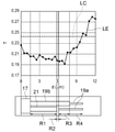
- FIG. 2 is an enlarged view of region II of FIG.
- the electrode finger 19 belonging to one comb tooth electrode 15 may be referred to as an electrode finger 19A
- the electrode finger 19 belonging to the other comb tooth electrode 15 may be referred to as an electrode finger 19B
- the bus bar 17 belonging to the one comb tooth electrode 15 may be referred to as a bus bar 17A
- the bus bar 17 belonging to the other comb tooth electrode 15 may be referred to as a bus bar 17B
- the dummy electrode 21 belonging to the one comb tooth electrode 15 may be referred to as a dummy electrode 21A
- the dummy electrode 21 belonging to the other comb tooth electrode 15 may be referred to as a dummy electrode 21B.
- the side of the center position between the pair of bus bars 17 may be referred to as "inside”, and the side opposite to the center position may be referred to as "outside”.
- the region between the pair of bus bars 17 has a so-called intersection region R6 and two outer regions R5 located on both sides in the D2 direction with respect to the intersection region R6.
- the intersection region R6 has a width (intersection width) at which the electrode fingers 19A and the electrode fingers 19B adjacent to each other overlap each other when viewed in the propagation direction of the elastic wave (D1 direction), and the plurality of electrode fingers 19A. And it can be said that the region extends along the arrangement of the plurality of electrode fingers 19B.
- the intersecting region R6 is a region sandwiched between a virtual line connecting the tips of the plurality of electrode fingers 19A and a virtual line connecting the tips of the plurality of electrode fingers 19B.
- the outer region R5 is the remaining region excluding the intersection region R6 from the region between the pair of bus bars 17.
- the intersecting region R6 has a central region R4 and two end regions R3 located on both sides in the D2 direction with respect to the central region R4.
- the central region R4 is an region including the central position between the pair of bus bars 17.
- the end region R3 is the remaining region excluding the central region R4 from the intersection region R6. That is, the end region R3 is a region from the edge of one (or the other) of the central region R4 on the bus bar 17 side to the edge of the intersection region R6 on the bus bar 17 side of the one (or the other).
- the end region R3 is the region where the tip of one of the electrode fingers 19A and 19B is located.
- the outer region R5 has, for example, a dummy region R1 on the bus bar 17 side and a gap region R2 on the intersection region R6 side.
- the dummy region R1 is a region where the dummy electrode 21 is located. That is, the dummy region R1 connects the tips of a plurality of dummy electrodes 21 protruding from the one (or the other) bus bar 17 from the inner (center region R4 side) edge of the one (or the other) bus bar 17.
- the gap region R2 is a region where the gap G1 between the dummy electrode 21 and the tip of the electrode finger 19 is located. That is, the gap region R2 is a region from the virtual line connecting the tips of the plurality of electrode fingers 19A (or 19B) to the virtual line connecting the tips of the plurality of dummy electrodes 21A (or 21B).
- the edge of the intersection region R6 on the bus bar 17 side (the edge of the end region R3 on the bus bar 17 side) and the edge of the outer region R5 on the bus bar 17 side (the edge of the dummy region R1 on the bus bar 17 side) are, for example, , It is a linear shape parallel to the propagation direction (D1 direction) of elastic waves.
- these edges may be curved, curved to form corners, beveled with respect to the propagation direction, or extend in a meandering manner. You may.
- the IDT electrode 11 may be apodized.
- the bus bar 17 may be bent or inclined with respect to the propagation direction of the elastic wave.
- the distance between the edge of the central region R4 on the bus bar 17 side and the edge of the intersection region R6 on the bus bar 17 side is constant regardless of the position in the D1 direction. It may be set to be.
- the edge of the gap region R2 on the bus bar 17 side is, for example, the distance from the edge of the intersection region R6 on the bus bar 17 side (in another viewpoint, the width of the gap region R2) regardless of the position in the D1 direction. It may be set to be constant. However, these intervals may differ depending on the position in the D1 direction.
- the relative relationship between the widths (lengths in the D2 direction) of a plurality of regions may be appropriately set.
- the width of the intersecting region R6 may be wider than the sum of the widths of the two outer regions R5.
- the above relationship may be established at the position where the width of the crossing region R6 is the widest.
- the width of the central region R4 may be wider than the sum of the widths of the two end regions R3.
- the width of one dummy region R1 may be wider than the width of one gap region R2.
- the specific value of the width of each area may be set as appropriate.
- the width of the intersection region R6, the width of the outer region R5, the width of the gap region R2, and the width of the dummy region R1 may be substantially the same as various known values, and are not particularly limited. An example of these width ranges is given by comparison with pitch p.
- the width of the intersection region R6 may be 10p or more and 200p or less.
- the width of each outer region R5 may be 0.2p or more and 10p or less.
- the width of each gap region R2 may be 0.1p or more and 9.9p or less.
- the width of each dummy region R1 may be 0.1p or more and 9.9p or less.
- a specific example of the width of the end region R3 will be described later in the description of the length of the widening portion 19b in the D2 direction.
- the width of the electrode finger 19 is constant over the entire length of the electrode finger 19.
- the width of the electrode finger 19 differs depending on the position in the length direction. This reduces, for example, transverse mode spurious. Specifically, it is as follows.
- each electrode finger 19 has a portion located in the intersection region R6 (central region R4 + end region R3) and one of the two outer regions R5 (gap region R2 +). It has a portion located in the dummy region R1).
- the portion located in the central region R4 is referred to as the main portion 19a.
- the electrode finger 19 has a width wider than the width of the main portion 19a (length in the D1 direction) in at least a part of the range (R3 + R2 + R1) from the edge of the central region R4 to the edge of the bus bar 17 on the central region R4 side. It has a widening portion 19b having the above.
- the widening portion 19b may be provided on either one or both. In the illustrated example, the widening portion 19b is provided on the root side.
- the widening portion 19b When the widening portion 19b is provided on the root side of the electrode finger 19, the widening portion 19b may be provided in any one or more of the end region R3, the gap region R2, and the dummy region R1. Further, the widening portion 19b may be located in a part of each region or may be located in the entire region. In the illustrated example, the widening portion 19b covers the entire three regions (R3, R2 and R1). Unlike the illustrated example, when the widening portion 19b is provided on the tip end side of the electrode finger 19, the widening portion 19b is located in the end region R3.
- the widening portion 19b may be located in the end region R3 by being provided on the root side and / or the tip side of the electrode finger 19.
- the portion of the intersection region R6 where the widening portion 19b is located is designated as the end region R3. May be defined.
- the widening portion 19b may be provided in an arbitrary region outside the central region R4, the length of the widening portion 19b in the D2 direction may be appropriately set. Further, as in the illustrated example, when the widening portion 19b extends over the entire range from the bus bar 17 to the edge of the central region R4, the length of the widening portion 19b in the D2 direction is described, for example, as described above.
- Patent Document 2 International Publication No. 2020/100419
- an elastic wave element having the IDT electrode 11 of the present embodiment is prototyped, and its frequency characteristics are measured. Specifically, as shown in FIG. 2 of the present disclosure, among the lengths of the widening portion 19b from the bus bar 17 to the central region R4 side, the length from the tip of the dummy electrode 21 to the central region R4 side (another). From the viewpoint, the sum of the width of one gap region R2 and the width of one end region R3) is defined as the "offset amount s1". A plurality of prototypes have been produced in which the width of each gap region R2 is 0.3p and the offset amount s1 is different from each other in the range of 0p or more and 10p or less.
- the offset amount s1 is 1p or more and 3p or less (particularly when it is 1.5p or more and 2.5p or less), the frequency characteristics are improved. Further, it is shown in the figure that there may be an offset amount whose characteristics are improved even outside the above range.
- the length of the widening portion 19b extending from the bus bar 17 toward the central region R4 is, for example, an offset amount s1 of more than 0p and 10p or less, 1p or more and 3p or less, or 1.5p or more and 2.5p or less. It may be set to be.
- the width of the end region R3 may be, for example, more than 0p and 10p or less, 0.5p or more and 2.5p or less, or 1.0p or more and 2.0p or less.
- the width of the central region R4 may be, for example, 65% or more of the width of the intersection region R6.
- the width of the widening portion 19b may be set as appropriate.
- the contents of Patent Document 2 may be incorporated for the width of the widening portion 19b.
- an elastic wave element having the IDT electrode 11 of the present embodiment is prototyped, and its frequency characteristics are measured.
- the duty of the widening portion 19b is 0.05 or more larger than the duty of the main portion 19a, for example, 0.40 or more and 0.80 or less, 0.40 or more and 0.65 or less, or 0.50. It may be 0.60 or less. And / or, the duty of the widening portion 19b may be set to a large value by a difference of 0.5 or more and 1.5 or less with respect to the duty of the main portion 19a.
- the width of the widening portion 19b may be 1.05 times or more or 1.1 times or more the width of the main portion 19a, or may be 2 times or less or 1.3 times or less, as described above. The lower and upper limits may be combined as appropriate.
- the density and thickness of the electrode finger 19 are, for example, constant over the entire length of the electrode finger 19. Therefore, it can be said that the widening portion 19b is a portion where the mass per unit length in the D2 direction is larger than that in the main portion 19a from another viewpoint.
- the width of the dummy electrode 21 may be appropriately set in a range of, for example, equal to or larger than the width of the main portion 19a and equal to or smaller than the width of the widening portion 19b.
- the width of the dummy electrode 21 may be the same as the width of the widening portion 19b of the electrode finger 19 (illustrated example), or may be the same as the width of the main portion 19a of the electrode finger 19. It may be different from both.
- FIG. 3 is a cross-sectional view taken along the line III-III of FIG.
- the composite substrate 3 has, for example, a support 29 and a piezoelectric layer 31 located on the upper surface of the support 29.
- the piezoelectric layer 31 constitutes at least a part of the upper surface of the composite substrate 3.
- the conductor layer 5 At least a portion constituting the resonator 7 is located on the upper surface of the piezoelectric layer 31. This makes it possible to convert elastic waves into electrical signals, as described above.
- the piezoelectric layer 31 constitutes the entire upper surface of the composite substrate 3, and the entire conductor layer 5 is located on the upper surface of the piezoelectric layer 31. And.
- a cavity 33 is formed between the support 29 and the piezoelectric layer 31.
- the cavity 33 overlaps the resonator 7 (in another aspect, the IDT electrode 11) in planar fluoroscopy. This facilitates, for example, exciting elastic waves in a particular mode, as described below.
- the cavity 33 may be configured by forming recesses on at least one of the upper surface of the support 29 and the lower surface of the piezoelectric layer 31.
- the cavity 33 is formed by forming a recess on the upper surface of the support 29.
- the support 29 has a support substrate 35 and a cavity layer 37 located on the upper surface of the support substrate 35.
- the cavity layer 37 is configured with an opening that penetrates the cavity layer 37 in the thickness direction, and this opening becomes the cavity 33.
- a recess may be formed on the upper surface of the integrally formed support 29.
- the thickness of the composite substrate 3 is, for example, substantially constant in the plane direction. Further, a specific value of the thickness may be appropriately set. For example, the thickness of the composite substrate 3 may be set so as to secure the strength of the wafer on which a large number of elements 1 are taken.
- the thickness of each layer (29, 31, 35, 37, and 37a and 37b described later) constituting the composite substrate 3 is, for example, in the plane direction except for a region where the thickness is reduced to form the cavity 33. Is almost constant.
- the thickness of the support substrate 35 may be appropriately set.
- the thickness of the support substrate 35 is thicker than the thickness of the piezoelectric layer 31 and the thickness of the cavity layer 37, respectively, and is thicker than the total of these.
- the material of the support substrate 35 may be appropriately set. Unlike the cavity layer 37, the support substrate 35 (in other words, the portion below the portion constituting the upper surface of the support 29) has little influence on the boundary conditions regarding the elastic waves propagating inside the piezoelectric layer 31. There is no. Therefore, the degree of freedom of the material of the support substrate 35 is high.
- the material of the support substrate 35 may be selected, for example, to improve the strength of the composite substrate 3.
- the material of the support substrate 35 is, for example, an insulating material.
- the insulating material is, for example, resin or ceramic.
- the insulating material may be a composite material in which a base material is impregnated with a resin, a composite material in which inorganic particles are mixed in a resin, or a single material that is not a composite material.
- the entire support substrate 35 may be made of one kind of material, or may be made of a plurality of materials by laminating layers made of different materials.
- the support substrate 35 may be made of a material having a coefficient of thermal expansion lower than that of the piezoelectric layer 31. In this case, for example, it is possible to reduce the probability that the frequency characteristic of the element 1 will change due to a temperature change. Examples of such a material include semiconductors such as silicon, single crystals such as sapphire, and ceramics such as aluminum oxide sintered bodies.
- the thickness of the cavity layer 37 may be appropriately set.
- the thickness of the cavity layer 37 is as small as possible within a range in which the upper surface of the cavity 33 (lower surface of the piezoelectric layer 31) and the lower surface of the cavity 33 (upper surface of the support substrate 35) do not come into contact with each other under the intended usage conditions. It may be, or it may be larger than such a size. Further, for example, the thickness of the cavity layer 37 may be smaller, equal to, or larger than the thickness of the piezoelectric layer 31.
- the material of the cavity layer 37 may be appropriately set. Since the cavity layer 37 (in other words, the portion constituting the upper surface of the support 29) is in contact with the lower surface of the piezoelectric layer 31, it affects the boundary conditions regarding the elastic waves propagating inside the piezoelectric layer 31. Therefore, as will be understood from the result of the simulation calculation described later, the characteristics of the element 1 can be improved by setting the material of the portion. However, regardless of the material, the acoustic difference from the cavity 33 (in other words, gas) is clear, and the action according to the present embodiment described later is exhibited.
- the acoustic impedance and / or the speed of sound may be relatively high or relatively low.
- Acoustic impedance is the product of density and speed of sound.
- the speed of sound here is the square root of the elastic modulus (for example, Young's modulus) divided by the density. In other words, the density and / or elastic modulus of the cavity layer 37 may be relatively high or relatively low.
- the material of the cavity layer 37 may have a relatively high electric resistance or may have a relatively low electric resistance. Regarding the latter, it can be said that the cavity layer 37 is a low resistance layer.
- the sheet resistance of the low resistance layer may be, for example, 5 ⁇ 10 3 ⁇ or more and 5 ⁇ 10 7 ⁇ or less. This value is based on International Publication No. 2019/022006. When the sheet resistance has frequency dependence, the above-mentioned sheet resistance value may be satisfied at any frequency in the range from the resonance frequency to the antiresonance frequency of the IDT electrode 11.
- the material of the cavity layer 37 include silicon (Si), silicon dioxide (SiO 2 ), aluminum nitride (AlN), hafnium oxide (HfO 2 ), tantalum pentoxide (Ta 2 O 5 ), and zirconium oxide. (ZrO 2 ) and titanium oxide (TIM 2 ) can be mentioned.
- the material of the low resistance layer for example, a material whose resistivity is adjusted by diffusing a metal or the like into an insulating material such as SiOx may be used.
- the cavity layer 37 may be entirely composed of one kind of material, or may be composed of a plurality of materials by laminating a plurality of layers made of different materials.
- FIG. 3B is a cross-sectional view showing an example of a cavity layer 37 composed of a plurality of layers, and corresponds to a part of FIG. 3A.
- the cavity layer 37 illustrated in FIG. 3B may have a first layer 37a and a second layer 37b overlapping the upper surface of the first layer 37a.
- the second layer 37b constitutes the upper surface of the cavity layer 37 and is in contact with the piezoelectric layer 31.
- the second layer 37b is thinner than, for example, the first layer 37a.
- the material of the second layer 37b can be selected in consideration of the boundary conditions regarding the elastic wave propagating in the piezoelectric layer 31.
- the first layer 37a can ensure the thickness of the cavity layer 37 (in another aspect, the height of the cavity 33), the strength of the cavity layer 37, and / or the bondability with the support substrate 35. ..
- the above-mentioned description of the material of the cavity layer 37 may be incorporated.
- the material of the first layer 37a or the second layer 37b may be Si, SiO 2 , AlN, HfO 2 , or the like described above.
- the second layer 37b may be the above-mentioned low resistance layer.
- the second layer 37b injects a predetermined element such as metal into the upper surface of the cavity layer 37 made of the material of the first layer 37a, or conversely releases a predetermined element from the upper surface of the cavity layer 37. It may be formed by letting it.
- the material exemplified as the material of the cavity layer 37 may be used for the support substrate 35.
- the material exemplified as the material of the support substrate 35 may be used for the cavity layer 37.
- the support 29 does not have the cavity layer 37 and the support substrate 35, and the entire support 29 may be integrally formed.
- the material of the support 29 in this case may be, for example, the material of the cavity layer 37 and / or the material exemplified as the material of the support 29.
- the piezoelectric layer 31 is composed of, for example, a single crystal having piezoelectricity.
- Examples of the material constituting such a single crystal include lithium tantalate (LiTaO 3 , hereinafter may be abbreviated as LT), lithium niobate (LiNbO 3 , hereinafter may be abbreviated as LN) and the like.
- a crystal (SiO 2 ) can be mentioned.
- the cut angle, planar shape and various dimensions may be set as appropriate.
- the piezoelectric layer 31 may be composed of polycrystals.
- the cut angle may be Euler angles ( ⁇ , ⁇ , ⁇ ) (0 ° ⁇ 10 °, 0 ° or more and 55 ° or less, 0 ° ⁇ 10 °).
- the LT is of rotational Y-cut X propagation.
- the Y-axis is inclined at an angle of 90 ° or more and 145 ° with respect to the normal line (D3 axis) of the piezoelectric layer 31.
- the X-axis is substantially parallel to the upper surface (D1 axis) of the piezoelectric layer 31.
- the X-axis and the D1 axis may be inclined to each other by a difference of ⁇ 10 ° or more and 10 ° or less in the XZ plane or the D1D2 plane.
- the cut angle may be Euler angles ( ⁇ , ⁇ , ⁇ ) (0 ° ⁇ 10 °, 15 ° ⁇ 10 °, 0 ° ⁇ 10 °). ..
- the LN is of rotational Y-cut X propagation.
- the Y-axis is inclined at an angle of 105 ° ⁇ 10 ° with respect to the normal line (D3 axis) of the piezoelectric layer 31.
- the cut angles may be Euler angles (0 ° ⁇ 10 °, 0 ° ⁇ 15 °, ⁇ ).
- ⁇ is 0 ° or more and 360 ° or less.
- the cut angle may be (0 ° ⁇ 5 °, 0 ° ⁇ 5 °, ⁇ ).
- the LN may be a Z-cut substrate.
- the thickness of the piezoelectric layer 31 may be appropriately set.
- the thickness of the piezoelectric layer 31 may be 1.5 p or less when expressed using a pitch p (a value excluding a peculiar pitch p as described above).
- the thickness of the piezoelectric layer 31 may be 0.3p or more and 0.6p or less.
- the lower surface of the piezoelectric layer 31 is exposed to, for example, the cavity 33.
- the lower surface of the piezoelectric layer 31 may be covered with a layer thinner than the piezoelectric layer 31 at least in a part (for example, the entire surface) including the region overlapping the cavity 33.
- the material of such a layer for example, the material exemplified as the material of the cavity layer 37 may be used.
- the thin layer may be a low resistance layer.
- the above-mentioned thin material made of a material different from the material of the piezoelectric layer 31 by injecting a predetermined element into the lower surface of the piezoelectric layer 31 or, conversely, discharging a predetermined element from the lower surface of the piezoelectric layer 31. Layers may be formed.
- the cavity 33 is sealed, for example.
- a gas is present in the cavity 33.
- the gas is, for example, air or an inert gas.
- nitrogen can be mentioned.
- the atmospheric pressure in the cavity 33 may be lower, equal to, or higher than that of the atmospheric pressure in a temperature environment where the element 1 is assumed to be used.
- the position, shape and dimensions of the cavity 33 may be appropriately set. As shown in FIG. 1, in planar fluoroscopy, the cavity 33 overlaps at least a portion of the resonator 7. In other words, the cavity 33 overlaps at least a portion of the IDT electrode 11. More specifically, the cavity 33 overlaps, for example, at least a portion (eg, all) of the central region R4.
- the edges 33a of the cavity 33 on both sides in the D2 direction overlap with, for example, the arrangement region of the IDT electrode 11. More specifically, the edge 33a is a range (end region R3, gap region) from the edge of the central region R4 on the bus bar 17 side to the edge of the outside of the bus bar 17 (opposite to the central region R4). It is located at either position of R2 and the dummy area R1).
- the edge portion 33a of the cavity 33 when it is said that the edge portion 33a of the cavity 33 is located within a predetermined range in planar fluoroscopy, the edge portion 33a may be located at the edge portion (boundary with another range) of the above range. ..
- the edge portion 33a may be located at the edge portion of the central region R4 on the bus bar 17 side or the outer edge portion of the bus bar 17. It goes without saying that tolerances may exist even if it is said that the edge portion 33a is located at the edge portion of a predetermined range in planar fluoroscopy, and to this extent, the edge portion 33a is located outside the predetermined range. May be good. Boundaries between adjacent regions may be interpreted as belonging to both unless otherwise specified and there is no contradiction.
- the distance from the outer edge of the bus bar 17 to the edge 33a of the cavity 33 may be referred to as the "penetration amount d" (FIG. 3A) of the support 29 (cavity layer 37).
- the edges 33b on both sides of the cavity 33 in the D1 direction are located, for example, outside the arrangement region of the resonator 7.
- the edge 33b is located outside the placement region of the IDT electrode 11.
- the edge portion 33b is, for example, described above. It may be located outside the filter placement area.
- the edge 33a on the bus bar 17 side of the cavity 33 is, for example, parallel to the propagation direction of the elastic wave (D1 direction), the edge of the intersection region R6, and / or the edge of the bus bar 17. From another viewpoint, the edge portion 33a has a constant distance from the edge portion of the intersection region R6 and / or the edge portion of the bus bar 17. Further, the edge portion 33a extends linearly.
- the edge portion 33a may have a different distance from the edge portion of the intersection region R6 and / or the edge portion of the bus bar 17, may be curved in a curved shape, or may be curved so as to form a corner portion. It may be, or it may extend in a meandering manner.
- the description of the position of the edge portion 33a described above may be established for a part of the edge portion 33a, for example, or most of the edge portion 33a (for example, the edge portion 33a is parallel to the D2 direction). It may hold for 80% or more of the length when projected on the D1 axis), or it may hold for all.
- the edge portion 33a has a portion inclined with respect to the D1 direction and / or a curved portion, for example, it is facilitated to scatter the elastic wave reflected by the edge portion 33a.
- edges 33b on both sides of the cavity 33 in the D1 direction extend linearly, for example, orthogonal to the D1 direction.
- the edge portion 33a may be inclined with respect to a direction orthogonal to the D1 direction, may be curved in a curved shape, may be curved so as to form a corner portion, or may meander. May extend to.
- the edge portion 33a on the bus bar 17 side of the cavity 33 is located within the arrangement region of the IDT electrode 11. Further, the plurality of electrode fingers 19 of the IDT electrode 11 have a widening portion 19b. By combining both, it is possible to reduce the spurious in the transverse mode and improve the characteristics of the element 1. Specifically, it is as follows.
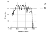
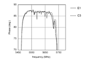
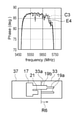
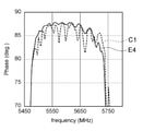
- FIGS. 4A and 4B are diagrams showing the characteristics of the resonator according to the comparative example and the embodiment.
- the horizontal axis indicates frequency.
- the vertical axis shows the impedance phase.
- the resonator 7 has a resonance frequency at which the absolute value of impedance is the minimum value and an antiresonance frequency at which the absolute value of impedance is the maximum value.
- the range between the resonance frequency and the antiresonance frequency it is said that the closer the impedance phase is to 90 °, the better the characteristics of the resonator 7. Further, outside the above range, the closer the impedance phase is to ⁇ 90 °, the better the characteristics of the resonator 7.
- the range on the horizontal axis generally corresponds to the range between the resonant frequency and the antiresonant frequency.
- FIG. 4A the characteristics of the first comparative example C1 and the second comparative example C2 are shown.
- the electrode finger 19 does not have the widening portion 19b.
- the edge portion 33a of the cavity 33 is located outside the IDT electrode 11.
- the edge portion 33a of the cavity 33 overlaps with the IDT electrode 11 as in the embodiment. Conditions other than the above are the same between the two comparative examples.
- both the first comparative example C1 and the second comparative example C2 there is a frequency in which the impedance phase specifically decreases within the frequency range in which the impedance phase should be 90 °. That is, a horizontal mode spurious is generated.
- the size and number of spurious are substantially the same in the first comparative example C1 and the second comparative example C2.
- the electrode finger 19 having no widening portion 19b is provided, whether or not the edge portion 33a of the cavity 33 overlaps with the IDT electrode 11 is determined with respect to the reduction of spurious in the transverse mode. There is no significant difference.
- FIG. 4B the characteristics of the third comparative example C3 and the first embodiment E1 are shown.
- the electrode finger 19 has the widening portion 19b as in the embodiment.
- the edge portion 33a of the cavity 33 is located outside the IDT electrode 11.
- the edge portion 33a of the cavity 33 overlaps with the IDT electrode 11 as in the embodiment. Conditions other than the above are the same among the three Comparative Examples and the First Example E1.
- the edge portion 33a on the bus bar 17 side of the cavity 33 is located in the arrangement region of the IDT electrode 11, and that the plurality of electrode fingers 19 of the IDT electrode 11 have the widening portion 19b.
- the size of the spurious is reduced for the first time by the combination with the matter. The reason is not always clear.
- the widening portion 19b reduces the speed of sound in the region outside the central region R4 by increasing the mass per unit length of the electrode finger 19 in the D2 direction.
- the support 29 reduces the speed of sound in the piezoelectric layer 31.
- the reason is that the boundary condition between the central region R4 and the region outside the central region R4 is conspicuous and the spurious in the transverse mode is reduced by superimposing both of them. For this reason, the length of the widening portion 19b in the D2 direction and the amount d of the support 29 penetrating into the IDT electrode 11 may be small. This is because the spurious in the transverse mode is still reduced to some extent.
- the edge 33a of the cavity 33 may be located inside the central region R4 rather than the edge on the bus bar 17 side of the central region R4.
- the area of the central region R4 is reduced.
- the impedance phase is lowered as a whole. Therefore, the limit position on the central region R4 side of the edge portion 33a may be the edge portion of the central region R4.
- Piezoelectric layer 31 Material: LN Cut angle: 105 ° rotation Y cut X propagation Thickness: 0.44 ⁇ m
- Cavity layer 37 Material: Si IDT electrode 11: Material: Al Thickness: 0.11 ⁇ m
- Pitch p 1.0 ⁇ m Width of bus bar 17: 1.5 ⁇ m Width of intersection area
- R6 40p Width of outer region
- R5 4.32 ⁇ m Width of dummy region
- R1 4 ⁇ m Width of gap region
- the thickness of the cavity layer 37 was set to be relatively thick. That is, it was assumed that the material of the support substrate 35 does not affect the boundary conditions of elastic waves.
- the conditions of the electrode finger 19 in the second comparative example C2, the third comparative example C3, and the first embodiment E1 are as follows.
- the entire Duty of the electrode finger 19 in the first Comparative Example C1 is the Duty of the main portion 19a.
- the configuration of the resonator 7 is the configuration exemplified in FIGS. 1, 2 and 3A (or FIG. 3B) unless otherwise specified.
- the various regions (R1 to R6) and the cavity 33 have a rectangular shape having long sides parallel to the propagation direction (D1 direction) of elastic waves.
- the widening portion 19b is provided on the root side of the electrode finger 19 and extends over a range (R1 + R2 + R3) from the bus bar 17 to the edge portion of the central region R4 on the bus bar 17 side.
- the edge 33a on the bus bar 17 side of the cavity 33 is set at an appropriate position within the range from the edge on the bus bar 17 side of the central region R4 to the edge on the outside of the bus bar 17 (opposite to the central region R4). You can do it. Within this range, for example, the effect of reducing spurious in the transverse mode is expected.
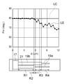
- examples of the characteristics of the resonator 7 will be shown for a plurality of cases in which the positions of the edge portions 33a (the amount of penetration d from another viewpoint) are different from each other.
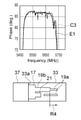
- FIGS. 5A to 5C and FIGS. 6A to 6C are diagrams showing the results of simulation calculations for the characteristics of the resonator 7.
- the upper part is the same as FIGS. 4A and 4B.
- the lower part schematically shows the positional relationship between the edge portion 33a of the cavity 33 and the IDT electrode 11.
- FIG. 5A corresponds to a comparative example (the third comparative example C3 described above) in which the edge portion 33a of the cavity 33 is located outside the IDT electrode 11.
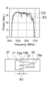
- FIG. 5B corresponds to an embodiment in which the edge portion 33a is located on the outer edge portion of the bus bar 17 (the above-described first embodiment E1).
- FIG. 5C corresponds to the second embodiment E2 in which the edge portion 33a is located in the middle of the bus bar 17.
- FIG. 6A corresponds to the third embodiment E3 in which the edge portion 33a is located in the dummy region R1.
- FIG. 6B corresponds to the fourth embodiment E4 in which the edge portion 33a is located at the edge portion of the intersection region R6.
- FIG. 6C corresponds to the fifth embodiment E5 in which the edge portion 33a is located at the edge portion of the central region R4.
- the conditions other than the position of the edge 33a of the cavity 33 are the same between the above-mentioned one comparative example and the five embodiments, and are the same as the conditions of the first embodiment E1 described with reference to FIG. 4B. Is.
- the distance between the edge portion 33a and the bus bar 17 is 1 ⁇ m.
- the amount of the cavity layer 37 (edge 33a) invading the central region R4 side from the outer edge of the bus bar 17 is 0 ⁇ m.
- the penetration amount d is 1 ⁇ m.
- the intrusion amount d is 3 ⁇ m.
- the intrusion amount d is 5.82 ⁇ m.
- the intrusion amount d is 7.5 ⁇ m.
- Evaluation index An evaluation index for evaluating the characteristics of the resonator 7 is defined. Then, based on this evaluation index, the influence of the position of the edge 33a on the bus bar 17 side of the cavity 33 on the characteristics of the resonator 7 is examined in detail.
- phase average value Pm is the value obtained by averaging the impedance phases over the frequency range from the resonance frequency to the antiresonance frequency.
- the overall magnitude of the impedance phase shall be evaluated by this phase mean value Pm.
- the value obtained by averaging the absolute value of the rate of change in the change of the impedance phase with respect to the change in frequency over the frequency range from the resonance frequency to the antiresonance frequency is used as the index T of the transverse mode.
- Transverse mode spurious shall be evaluated by this index T.
- the index T is 0.
- the changes in the phase mean value Pm and the index T with respect to the change in the intrusion amount d were obtained by simulation calculation for each material of the cavity layer 37.
- the simulation conditions are the same among the plurality of simulation cases except for the material of the cavity layer 37 and the penetration amount d, and are the same as the simulation cases described with reference to FIGS. 4A to 6C.
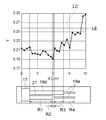
- (Si) 7A and 7B are diagrams showing the characteristics of the resonator 7 in which the material of the cavity layer 37 is Si.
- the horizontal axis shows the intrusion amount d.
- the vertical axis indicates the index T.
- the vertical axis shows the phase mean value Pm.
- the lower part of FIGS. 7A and 7B schematically shows the shape of the IDT electrode 11.
- the position of the horizontal axis in the upper row and the position in the horizontal direction in the IDT electrode 11 in the lower row correspond to each other.
- 0 ⁇ m in the upper row corresponds to the outer edge of the bus bar 17 in the lower row.
- the upper 1.5 ⁇ m corresponds to the inner edge of the lower bus bar 17.
- the line LE shows the characteristics of the embodiment.
- the line LC shows the characteristics of the comparative example. That is, the line LC shows the value of the index T or the phase average value Pm when the intrusion amount d is a negative value (more specifically, -1 ⁇ m) regardless of the position on the horizontal axis.
- the change in the index T with respect to the change in the intrusion amount d is as follows.
- the index T is smaller than the index T in the comparative example.
- the index T generally decreases.
- the edge 33a of the cavity 33 approaches the gap region R2
- the index T stops lowering. After that, the index T increases slightly before the edge portion 33a reaches the central region R4.
- the edge portion 33a is located in the central region R4 and the intrusion amount d is further increased, the index T becomes larger than the index T in the comparative example.
- the relationship between the range where the edge 33a of the cavity 33 is located and the size of the index T is as follows.
- the index T is reduced as compared with the comparative example.
- the index T is roughly equal to or smaller than the size when the intrusion amount d is 0 ⁇ m. More strictly, when the edge portion 33a is located in the range of R1 + R2, the index T is equal to or less than the size when the intrusion amount d is 0 ⁇ m.
- the index T is the smallest.
- a range having a width of about 10 times the width of the gap region R2 centered on the gap region R2 can be mentioned.
- a range of the dummy region R1 adjacent to the gap region R2 and having a width of about 5 times the gap region R2 can be mentioned.
- the change in the phase mean value Pm with respect to the change in the intrusion amount d is as follows.
- the phase mean value Pm is substantially the same as the phase mean value Pm of the comparative example (slightly larger). Even if the intrusion amount d increases from 0 ⁇ m, the phase mean value Pm does not change significantly, and a state substantially equivalent to the phase mean value Pm of the comparative example is maintained. After that, the phase average value Pm decreases slightly before the edge portion 33a of the cavity 33 reaches the central region R4. Then, the phase mean value Pm is smaller than the phase mean value Pm of the comparative example.
- phase mean value Pm is the phase mean value Pm of the comparative example. Generally equal or better. Further, when the edge portion 33a is located in the range of R1 + R2, the phase mean value Pm is larger than the phase mean value Pm of the comparative example.
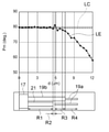
- (SiO 2 ) 8A and 8B are diagrams showing the characteristics of the resonator 7 in which the cavity layer 37 has a first layer 37a made of Si and a second layer 37b made of SiO 2 , and is similar to FIGS. 7A and 7B. It is a figure of.
- the thickness of the second layer 37b is 0.1 ⁇ m.
- the change in the index T with respect to the change in the intrusion amount d is substantially the same as in FIG. 7A.
- the rise of the index T starts earlier after the edge portion 33a of the cavity 33 is close to the gap region R2 and the index T stops lowering.
- the relationship between the range where the edge 33a of the cavity 33 is located and the size of the index T is as follows.
- the index T is reduced as compared with the comparative example as in FIG. 7A.
- the index T is not smaller than the size when the intrusion amount d is 0 ⁇ m.
- the index T is equal to or smaller than the size when the intrusion amount d is 0 ⁇ m, as in FIG. 7A.
- the index T is the smallest.
- a range of the dummy area R1 that is adjacent to the gap area R2 and has a width of about 5 times the gap area R2 can be mentioned.
- the relationship between the range where the edge 33a of the cavity 33 is located and the size of the phase average value Pm is as follows.
- the phase mean value Pm is the phase mean value Pm of the comparative example. It is almost the same.
- (Low resistance layer) 9A and 9B are diagrams showing the characteristics of the resonator 7 in which the cavity layer 37 has a first layer 37a made of Si and a second layer 37b made of a low resistance layer. It is a similar figure.
- the thickness of the second layer 37b is 2 nm.
- the resistivity of the second layer 37b is 2.5 ⁇ ⁇ cm at 5500 MHz. That is, the sheet resistance of the second layer 37b is 1.25 ⁇ 107 ⁇ .
- the sheet resistance of the second layer 37b is adjusted by subjecting the upper surface of the first layer 37a to a predetermined treatment, and its density and elastic modulus are substantially the same as those of Si.
- FIG. 9A the change in the index T with respect to the change in the intrusion amount d, and the relationship between the range where the edge 33a of the cavity 33 is located and the size of the index T are substantially the same as those in FIG. 7A.
- FIG. 9B the change in the phase average value Pm with respect to the change in the intrusion amount d, and the relationship between the range where the edge portion 33a of the cavity 33 is located and the size of the phase average value Pm are substantially the same as in FIG. 7B.
- (AlN) 10A and 10B are diagrams showing the characteristics of the resonator 7 in which the cavity layer 37 has a first layer 37a made of Si and a second layer 37b made of AlN, and is similar to FIGS. 7A and 7B. It is a figure.
- the thickness of the second layer 37b is 0.1 ⁇ m.
- the change in the index T with respect to the change in the intrusion amount d, and the relationship between the range where the edge 33a of the cavity 33 is located and the size of the index T are substantially the same as those in FIG. 8A.
- the index T is defined as the smallest range, for example, the range described in FIG. 8A (the range of the dummy area R1 that is adjacent to the gap area R2 and has a width of about 5 times the gap area R2).
- a range in which half of the gap region R2 on the dummy region R1 side is added to the range can be mentioned.
- the change in the phase mean value Pm with respect to the change in the intrusion amount d, and the relationship between the range where the edge 33a of the cavity 33 is located and the size of the phase mean value Pm are substantially the same as in FIG. 8B.
- FIGS. 7A and 7B are diagrams showing the characteristics of the resonator 7 in which the cavity layer 37 has a first layer 37a made of Si and a second layer 37b made of HfO 2 , and is similar to FIGS. 7A and 7B. It is a figure of.
- the thickness of the second layer 37b is 0.1 ⁇ m.
- the change in the index T with respect to the change in the intrusion amount d is substantially the same as in FIG. 8A.
- the index T when the intrusion amount d is 0 is different from the previous examples and is substantially the same as the index T of the comparative example. Further, when the decrease of the index T stops decreasing and then increases, it becomes equivalent to the value of the index T of the comparative example earlier than the previous examples.
- the relationship between the range where the edge 33a of the cavity 33 is located and the size of the index T is as follows.
- the index T is roughly equal to or less than the index T of the comparative example. be.
- the index T is roughly equal to or smaller than the size when the intrusion amount d is 0 ⁇ m.
- the index T is the smallest when the edge 33a is within the range of the gap region R2 and / or its surroundings.
- a range similar to that in FIG. 8A (a range of the dummy area R1 adjacent to the gap area R2 and having a width of about 5 times the gap area R2) can be mentioned. can.
- HfO 2 is a relatively high density material.
- the densities of LN and LT are 4 g / cm 3 or more and 8 g / cm 3 or less.
- the density of HfO 2 is 9 g / cm 3 or more and 11 g / cm 3 or less.
- the densities of Si, SiO 2 and AlN are 2 g / cm 3 or more and 4 g / cm 3 or less. Therefore, the material constituting the upper surface of the support 29 (for example, the entire cavity layer 37 or the second layer 37b) may be, for example, a material having a density smaller than the density of the material of the piezoelectric layer 31.
- Si (FIG. 7A) and SiO 2 (FIG. 8A) have relatively close densities (2 g / cm 3 or more and 3 g / cm 3 or less).
- the material of the cavity layer 37 is Si
- the value of the index T itself is small
- the amount of reduction of the index T with respect to the index T of the comparative example is large
- the range is wide. The reason is that the speed of sound in SiO 2 is relatively low, and elastic waves leaking from the central region R4 tend to concentrate in the portion near the edge 33a of the cavity layer 37.
- the speed of sound of SiO 2 (square root of the value obtained by dividing the elastic modulus by the density) is 5000 m / s or more and 6000 m / s or less, and the speed of sound of Si is 7000 m / s or more and 9000 m / s or less. Therefore, the material constituting the upper surface of the support 29 (for example, the entire cavity layer 37 or the second layer 37b) may be, for example, a material having a sound velocity of 7,000 m / s or more.
- the duty of the widening portion 19b was set to 0.60.
- the characteristics obtained by the simulation calculation are shown for the case where the Duty of the widening portion 19b is different from 0.60.
- the conditions other than the duty of the widening portion 19b are the same as those in FIG. 7A.
- the cavity layer 37 is entirely composed of Si.
- 12A and 12B are diagrams showing the characteristics of the resonator 7 having a duty of 0.70 in the widening portion 19b, and are the same diagrams as those in FIGS. 7A and 7B.
- 13A and 13B are diagrams showing the characteristics of the resonator 7 having a duty of 0.80 in the widening portion 19b, and are the same views as those in FIGS. 7A and 7B.
- the same tendency as in FIGS. 7A and 7B can be seen for the index T and the phase mean value Pm.
- the position of the edge 33a of the cavity 33 where the index T is the minimum is the position adjacent to the gap region R2 in the dummy region R1
- the index is The position of the edge portion 33a where T is the minimum is located in the end region R3.
- the position of the edge portion 33a where the index T is the minimum is located in the widening portion 19b.
- FIG. 7A is the smallest.
- FIG. 14B is a diagram similar to FIG. 4A showing the characteristics of the first comparative example C1 of FIG. 4A and the fourth embodiment E4 of FIG. 6B.
- the electrode finger 19 does not have the widening portion 19b, and the edge portion 33a of the cavity 33 is located outside the arrangement region of the IDT electrode 11. ing.
- the width of the bus bar 17 is 1.5 ⁇ m.
- FIG. 14A is a diagram similar to FIG. 4A showing the characteristics of the fourth comparative example C4 and the sixth embodiment E6.
- the width of the bus bar 17 is 0.3 ⁇ m.
- Other conditions in the fourth comparative example C4 are the same as those in the first comparative example C1.
- Other conditions in the sixth embodiment E6 are the same as those in the fourth embodiment E4.
- the edge 33a of the cavity 33 is located in the arrangement region of the IDT electrode 11, and the widening portion 19b is provided on the electrode finger 19, so that the width of the bus bar 17 does not depend on the width of the bus bar 17. The effect of reducing the spurious of the mode can be obtained.
- 15A and 15B are diagrams showing changes in the characteristics of the resonator 7 with respect to changes in the width of the bus bar 17.
- the horizontal axis BW indicates the width of the bus bar 17.
- the vertical axis of FIG. 15A indicates the index T.
- the vertical axis of FIG. 15B shows the phase mean value Pm.
- the polygonal line in the figure shows the characteristics in the embodiment. Further, in the figure, points showing the characteristics of the first Comparative Example C1, the fourth Example E4, the fourth Comparative Example C4, and the sixth Example E6 shown in FIGS. 14A and 14B are shown. From these figures, it can be seen that the actions described so far do not depend on the width of the bus bar 17.
- the elastic wave element 1 has a support 29, a piezoelectric layer 31 on the support 29, and an IDT electrode 11 on the piezoelectric layer 31.
- a cavity 33 that overlaps with the IDT electrode 11 in planar fluoroscopy is formed between the piezoelectric layer 31 and the support 29.
- the IDT electrode 11 has a first bus bar and a second bus bar (bus bars 17A and 17B), and a plurality of first electrode fingers and a plurality of second electrode fingers (electrode fingers 19A and 19B).
- the bus bars 17A and 17B face each other in the direction (D2 direction) intersecting the first direction (D1 direction).
- the plurality of electrode fingers 19A extend in parallel with each other from the bus bar 17A toward the bus bar 17B.
- the plurality of electrode fingers 19B extend in parallel with each other from the bus bar 17B toward the bus bar 17A.
- the plurality of electrode fingers 19A and the plurality of electrode fingers 19B are alternately arranged in the D1 direction.
- a region extending along an array of a plurality of electrode fingers 19A and a plurality of electrode fingers 19B at an intersecting width in which the electrode fingers 19A and the electrode fingers 19B adjacent to each other overlap each other when viewed in the D1 direction. Is referred to as an intersection region R6.
- the intersecting region R6 has a central region R4 and a first end region and a second end region (two end regions R3).
- the central region R4 includes a central position between the two bus bars 17.
- Each end region R3 is a region from the edge portion of the central region R4 on the bus bar 17 side to the edge portion of the intersection region R6 on the bus bar 17 side.
- the cavity 33 overlaps the central region R4.
- the edge of the cavity 33 on the bus bar 17A side is located within a range from the edge of the central region R4 on the bus bar 17A side to the edge of the bus bar 17A on the opposite side (outer side) of the central region R4.
- Each of the plurality of electrode fingers 19A has a first portion (main portion 19a) and a second portion (widening portion 19b).
- the main portion 19a is located in the central region R4.
- the widened portion 19b of the electrode finger 19A is located on the bus bar 17A side or the bus bar 17B side (in this embodiment, the bus bar 17A side) with respect to the central region R4.
- the mass on the lower surface of the plurality of electrode fingers 19A per unit length in the second direction (D2 direction) orthogonal to the D1 direction has a larger value in the widening portion 19b than in the main portion 19a.
- the widening portion 19b can reduce the speed of sound in the region where the IDT electrode 11 is arranged and in the region outside the central region R4. Further, the support 29 can reduce the speed of sound in the region where the IDT electrode 11 is arranged and in the region outside the central region R4. And, by this combination, the spurious of the transverse mode can be reduced.
- the width of the second portion may be wider than the width of the first portion (main portion 19a).
- the mass per unit length of the second portion can be increased by patterning the conductor layer 5.
- the embodiment may also be included in the technique according to the present disclosure.
- the mass per unit length can be easily increased. As a result, it is advantageous in terms of cost.
- the widened portion 19b of the electrode finger 19A may be located on the bus bar 17A side with respect to the central region R4. That is, the widening portion 19b may be located on the root side of the electrode finger 19.
- a second portion (widening portion 19b) is provided on the tip end side of the electrode finger 19 (this aspect is also included in the technique according to the present disclosure). Good), it is easier to reduce the spurious in the transverse mode.
- the second portion is provided on the tip side in addition to the root side of the electrode finger 19, for example, the characteristics on the higher frequency side than the antiresonance frequency are improved.
- the widening portion 19b of the electrode finger 19A may extend from the bus bar 17A to the edge of the central region R4 on the bus bar 17A side (R1 + R2 + R3).
- the spurious in the transverse mode is reduced as compared with the embodiment in which the widening portion 19b is located only in a part of the range of R1 + R2 + R3 (the embodiment may also be included in the technique according to the present disclosure). The effect is improved.
- the edge 33a on the bus bar 17A side of the cavity 33 is located at any position in the range from the edge of the crossing region R6 on the bus bar 17A side to the edge of the bus bar 17A on the opposite side (outer side) of the central region R4. You can do it.
- the IDT electrode 11 may have a first dummy electrode and a second dummy electrode (dummy electrodes 21A and 21B).
- the dummy electrode 21A projects from the bus bar 17A toward the bus bar 17B between the plurality of electrode fingers 19A, and the tips of the dummy electrodes 21A face each other with the plurality of electrode fingers 19B. The same applies to the dummy electrode 21B.
- the edge 33a on the bus bar 17A side of the cavity 33 is located at any position in the range (R1 + R2) from the tips of the plurality of dummy electrodes 21A to the edge on the opposite side (outside) of the central region R4 of the bus bar 17A. You can do it.
- the above-mentioned effect is further improved. That is, there is a high probability that the effect of reducing spurious in the transverse mode will be achieved. The probability that the phase mean value Pm becomes small is reduced.
- the Duty of the widening portion 19b is set so that the effect of reducing the spurious in the transverse mode is relatively large, it is facilitated to minimize the spurious in the transverse mode.
- the edge 33a on the bus bar 17A side of the cavity 33 is located at any position in the range (R1 + R2 + R3) from the edge of the central region R4 on the bus bar 17A side to the edge of the bus bar 17A on the central region R4 side (inside). You can do it.
- the index T tends to become smaller as the intrusion amount d increases from 0 ⁇ m, so that it is easy to minimize the spurious in the transverse mode.
- the material, cut angle, and thickness of the piezoelectric layer 31 may have a relationship in which the amplitude of the A1 mode lamb wave is the largest among the elastic waves excited by the IDT electrode 11. That is, the element 1 may utilize the A1 mode lamb wave.
- the support 29 constitutes the upper surface of the support 29 and has a layer whose density is lower than the density of the piezoelectric layer 31 (for example, the entire support 29, the cavity layer 37 or the second layer 37b). It's okay. And / or the support 29 constitutes the upper surface of the support 29 and has a layer having a sound velocity of 7,000 m / s or more (for example, the entire support 29, the cavity layer 37 or the second layer 37b). You can do it.
- the effect of reducing spurious in the transverse mode can be improved.
- the range of the intrusion amount d from which the effect of reducing spurious in the transverse mode can be obtained can be widened.
- the elastic wave element may utilize a so-called piston mode. Even in this case, the same effect as that of the first embodiment is obtained. Specifically, it is as follows.
- 16A and 16B are diagrams showing the characteristics of the resonator according to the second embodiment, and are the same diagrams as those of FIGS. 7A and 7B.
- the bus bar 217 has a plurality of (only one is shown) openings 217h arranged in the propagation direction of elastic waves (vertical direction on the paper surface). ing. Further, the dummy electrode 21 (in other words, the dummy region R1) is not provided.
- the electrode finger 19 has a widening portion 19c not only on the root side but also on the tip side. As shown in the upper part of FIGS. 16A and 16B, the same tendency as that of the first embodiment was confirmed with respect to the index T and the phase mean value Pm even with the above configuration.
- FIG. 17 is a circuit diagram schematically showing the configuration of a duplexer 101 (for example, a duplexer) as a usage example of the element 1.
- a duplexer 101 for example, a duplexer
- the comb tooth electrode 15 is schematically shown by a bifurcated fork shape, and the reflector 13 is a single line with both ends bent. It is represented by.
- the demultiplexer 101 for example, has a transmission filter 109 that filters the transmission signal from the transmission terminal 105 and outputs the signal to the antenna terminal 103, and the demultiplexer 101 filters the reception signal from the antenna terminal 103 and outputs the signal to the pair of reception terminals 107. It has a reception filter 111.
- the transmission filter 109 is composed of, for example, a ladder type filter in which a plurality of resonators 7 (7S and 7P) are connected in a ladder type. That is, the transmission filter 109 includes a plurality of (or even one) series resonators 7S connected in series between the transmission terminal 105 and the antenna terminal 103, a line (series arm) thereof, and a reference potential portion (a reference potential portion). It has a plurality of (or even one) parallel resonators 7P (parallel arms) connecting the reference numerals (omitted).
- the reception filter 111 is configured to include, for example, a resonator 7 and a multiple mode type filter (including a double mode type filter) 113.
- the multimode filter 113 has a plurality of (three in the illustrated example) IDT electrodes 11 arranged in the propagation direction of elastic waves, and a pair of reflectors 13 arranged on both sides thereof.
- the plurality of IDT electrodes 11 (and reflectors 13) of the duplexer 101 may be provided on one composite substrate 3 or may be dispersedly provided on two or more composite substrates 3.
- the plurality of resonators 7 constituting the transmission filter 109 may be provided on the same composite substrate 3.
- the resonator 7 and the multiple mode filter 113 constituting the reception filter 111 may be provided on the same composite substrate 3, for example.
- the transmission filter 109 and the reception filter 111 may be provided on the same composite substrate 3 or on different composite substrates 3 from each other, for example.
- a plurality of series resonators 7S may be provided on the same composite substrate 3, and a plurality of parallel resonators 7P may be provided on another same composite substrate 3.
- FIG. 17 is just an example of the configuration of the demultiplexer 101. Therefore, for example, the reception filter 111 may be configured by a ladder type filter like the transmission filter 109. Further, the transmission filter 109 may have a multiple mode type filter 113.
- the duplexer 101 is not limited to the duplexer, and may be, for example, a duplexer or a multiplexer including three or more filters.
- the resonator 7 and the multiple mode filter 113 may be regarded as the element 1, respectively. Further, each of the transmission filter 109 and the reception filter 111 may be regarded as the element 1. Further, the duplexer 101 may be regarded as the element 1.
- FIG. 18 is a block diagram showing a main part of the communication device 151 as a usage example of the element 1 (from another viewpoint, the duplexer 101).
- the communication device 151 performs wireless communication using radio waves, and includes a demultiplexer 101.
- the transmission information signal TIS including information to be transmitted is modulated and frequency-raised (converted to a high-frequency signal having a carrier frequency) by an RF-IC (Radio Frequency Integrated Circuit) 153, and the transmission signal TS is performed. It is said that.
- the transmission signal TS has unnecessary components other than the pass band for transmission removed by the bandpass filter 155, is amplified by the amplifier 157, and is input to the demultiplexer 101 (transmission terminal 105). Then, the demultiplexer 101 (transmission filter 109) removes unnecessary components other than the passing band for transmission from the input transmission signal TS, and outputs the removed transmission signal TS from the antenna terminal 103 to the antenna 159. ..
- the antenna 159 converts the input electric signal (transmission signal TS) into a radio signal (radio wave) and transmits the radio signal (radio wave).
- the radio signal (radio wave) received by the antenna 159 is converted into an electric signal (received signal RS) by the antenna 159 and input to the demultiplexer 101 (antenna terminal 103).
- the demultiplexer 101 removes unnecessary components other than the passing band for reception from the input reception signal RS and outputs the signal from the reception terminal 107 to the amplifier 161.
- the output received signal RS is amplified by the amplifier 161 and unnecessary components other than the passing band for reception are removed by the bandpass filter 163. Then, the frequency of the received signal RS is reduced and demodulated by the RF-IC153 to obtain the received information signal RIS.
- the transmission information signal TIS and the reception information signal RIS may be low frequency signals (baseband signals) containing appropriate information, and are, for example, analog audio signals or digitized audio signals.
- the pass band of the radio signal may be appropriately set and may follow various known standards.
- the modulation method may be phase modulation, amplitude modulation, frequency modulation, or a combination of any two or more of these.
- the direct conversion system is exemplified as the circuit system, other appropriate circuit systems may be used, and for example, a double superheterodyne system may be used.
- FIG. 18 schematically shows only the main part, and a low-pass filter, an isolator, or the like may be added at an appropriate position, or the position of the amplifier or the like may be changed.
- the bus bar 17A and the bus bar 217 are examples of the first bus bar, respectively.
- the bus bar 17B and the bus bar 217 are examples of the second bus bar, respectively.
- the electrode finger 19A is an example of the first electrode finger.
- the electrode finger 19B is an example of the second electrode finger.
- the end region R3 on the bus bar 17A side is an example of the first end region.
- the end region R3 on the bus bar 17B side is an example of the second end region.
- the main part 19a is an example of the first part.
- the widening portion 19b and the widening portion 19c are examples of the second portion, respectively.
- the dummy electrode 21A is an example of the first dummy electrode.
- the dummy electrode 21B is an example of the second dummy electrode.
- RF-IC153 is an example of an integrated circuit element.
- the method of increasing the mass on the lower surface of the electrode finger at the second portion per unit length in the second direction is not limited to the method of using the second portion as the widening portion.
- the thickness of the second part may be made thicker than the thickness of the first part, or an insulating or conductive additional film may be provided only on the second part of the first part and the second part. It's okay.
- the portion on the second portion may be made thicker than the portion on the first portion. Two or more of the methods described so far may be combined.
- the mass on the lower surface of the electrode finger may include not only the mass of the electrode finger itself but also the mass of the member overlapping the electrode finger.
- the widening portion is provided on both the first electrode finger and the second electrode finger. Further, both the edge of the cavity on the first busbar side and the edge of the cavity on the second busbar side overlapped with the IDT electrode. However, the widening portion is provided only on one of the first electrode finger and the second electrode finger, and / or only one of the edge portion on the first bus bar side and the edge portion on the second bus bar side overlaps with the IDT electrode. You may. The range of positions of the edges of the cavities examined with reference to FIGS. 7A-16B may be combined with an electrode shape different from the illustrated example.
Abstract
Between a piezoelectric layer and a support, a cavity which overlaps an IDT electrode in a see-through plan view is formed. An intersection region in which first electrode fingers overlap second electrode fingers has a central region and two edge regions which are located on either side of the central region. The cavity overlaps the central region. An edge part of the cavity on a first bus bar side is located within a range from an edge part of the central region which is on the first bus bar side to an edge part of the first bus bar which is opposite to the central region. The first electrode fingers extending from the first bus bar each have a first portion which is located in the central region and a second portion which is located on the first bus bar side or a second bus bar side of the central region. The mass per unit length of the first electrode fingers on the lower surface is such that the value thereof for the first portions is greater than the value thereof for the second portions.
Description
本開示は、弾性波から電気信号への変換、及び電気信号から弾性波への変換の少なくとも一方が可能な弾性波素子、並びに当該弾性波素子を含む通信装置に関する。
The present disclosure relates to an elastic wave element capable of converting an elastic wave to an electric signal and at least one of an electric signal to an elastic wave, and a communication device including the elastic wave element.
弾性波素子として、圧電層と、圧電層上に位置するIDT(Interdigital Transducer)電極とを有するものが知られている(例えば、下記特許文献1又は2)。IDT電極は、1対の櫛歯電極を有する。各櫛歯電極は、バスバーと、バスバーから互いに並列に延びる複数の電極指とを有する。1対の櫛歯電極は、互いに噛み合うように配置される。
As an elastic wave element, one having a piezoelectric layer and an IDT (Interdigital Transducer) electrode located on the piezoelectric layer is known (for example, Patent Document 1 or 2 below). The IDT electrode has a pair of comb-tooth electrodes. Each comb tooth electrode has a bus bar and a plurality of electrode fingers extending in parallel with each other from the bus bar. A pair of comb tooth electrodes are arranged so as to mesh with each other.
特許文献1では、圧電層は、上面に空洞が形成された支持体の上面に重ねられている。IDT電極は、平面透視において空洞に重なるように設けられている。平面透視において、空洞の縁部は、IDT電極の外側に位置するか、バスバーに重なっている。特許文献2では、電極指は、バスバーに接続されている根元部分の幅が他の部分の幅よりも広くされている。なお、これらの文献の内容は、本願において参照による援用がなされてよい。
In Patent Document 1, the piezoelectric layer is superposed on the upper surface of a support having a cavity formed on the upper surface. The IDT electrode is provided so as to overlap the cavity in planar fluoroscopy. In planar fluoroscopy, the edge of the cavity is located outside the IDT electrode or overlaps the bus bar. In Patent Document 2, the width of the root portion of the electrode finger connected to the bus bar is wider than the width of the other portion. The contents of these documents may be incorporated by reference in the present application.
本開示の一態様に係る弾性波素子は、支持体と、前記支持体上の圧電層と、前記圧電層上のIDT電極と、を有している。前記圧電層と前記支持体との間に、平面透視において前記IDT電極と重なる空洞が構成されている。前記IDT電極は、第1方向に交差する方向において互いに対向している第1バスバー及び第2バスバーと、前記第1バスバーから前記第2バスバーに向かって互いに並列に延びている複数の第1電極指と、前記第2バスバーから前記第1バスバーに向かって互いに並列に延びている複数の第2電極指と、を有している。前記複数の第1電極指と複数の第2電極指とは、前記第1方向に交互に配列されている。互いに隣り合っている第1電極指と第2電極指とを前記第1方向に見たときに両者が互いに重複する交差幅で、前記複数の第1電極指及び前記複数の第2電極指の配列に沿って延びている領域を交差領域と呼称する。該交差領域は、中央領域と、第1端部領域と、第2端部領域とを有している。前記中央領域は、前記第1バスバーと前記第2バスバーとの間の中央位置を含む。前記第1端部領域は、前記中央領域の前記第1バスバー側の縁部から前記交差領域の前記第1バスバー側の縁部までの間の領域である。前記第2端部領域は、前記中央領域の前記第2バスバー側の縁部から前記交差領域の前記第2バスバー側の縁部までの間の領域である。前記空洞は、前記中央領域に重なっている。前記空洞の前記第1バスバー側の縁部は、前記中央領域の前記第1バスバー側の縁部から前記第1バスバーの前記中央領域とは反対側の縁部までの範囲内に位置している。前記複数の第1電極指のそれぞれは、前記中央領域に位置している第1部位と、前記中央領域に対して前記第1バスバー側又は前記第2バスバー側に位置する第2部位と、を有している。前記第1方向に直交する第2方向における単位長さ当たりの、前記複数の第1電極指の下面上の質量は、前記第1部位における値よりも前記第2部位における値が大きい。
The elastic wave element according to one aspect of the present disclosure has a support, a piezoelectric layer on the support, and an IDT electrode on the piezoelectric layer. A cavity that overlaps with the IDT electrode in planar fluoroscopy is formed between the piezoelectric layer and the support. The IDT electrodes include a first bus bar and a second bus bar facing each other in a direction intersecting the first direction, and a plurality of first electrodes extending in parallel with each other from the first bus bar toward the second bus bar. It has a finger and a plurality of second electrode fingers extending in parallel with each other from the second bus bar toward the first bus bar. The plurality of first electrode fingers and the plurality of second electrode fingers are alternately arranged in the first direction. When the first electrode finger and the second electrode finger adjacent to each other are viewed in the first direction, the cross widths of the first electrode finger and the second electrode finger overlap each other, and the plurality of first electrode fingers and the plurality of second electrode fingers have an intersecting width. The region extending along the array is called an intersection region. The intersection region has a central region, a first end region, and a second end region. The central region includes a central position between the first bus bar and the second bus bar. The first end region is a region between the edge of the central region on the first busbar side and the edge of the intersection region on the first busbar side. The second end region is a region between the edge of the central region on the second busbar side and the edge of the intersection region on the second busbar side. The cavity overlaps the central region. The first busbar-side edge of the cavity is located within the range from the first busbar-side edge of the central region to the opposite edge of the first busbar to the central region. .. Each of the plurality of first electrode fingers has a first portion located in the central region and a second portion located on the first busbar side or the second busbar side with respect to the central region. Have. The mass on the lower surface of the plurality of first electrode fingers per unit length in the second direction orthogonal to the first direction has a larger value in the second portion than the value in the first portion.
本開示の一態様に係る通信装置は、上記弾性波素子を含むフィルタと、前記フィルタと接続されているアンテナと、前記フィルタを介して前記アンテナと接続されている集積回路素子と、を有している。
The communication device according to one aspect of the present disclosure includes a filter including the elastic wave element, an antenna connected to the filter, and an integrated circuit element connected to the antenna via the filter. ing.
以下、本開示に係る実施形態について、図面を参照して説明する。以下の説明で用いられる図は模式的なものである。従って、例えば、図面上の寸法比率等は現実のものとは必ずしも一致していない。
Hereinafter, embodiments according to the present disclosure will be described with reference to the drawings. The figures used in the following description are schematic. Therefore, for example, the dimensional ratios on the drawings do not always match the actual ones.
本開示に係る弾性波素子は、いずれの方向が上方または下方とされてもよい。ただし、以下では、便宜的に、D1軸、D2軸およびD3軸からなる直交座標系を定義するとともに、D3軸の正側を上方として、上面または下面等の用語を用いることがある。また、平面視または平面透視という場合、特に断りがない限りは、D3方向に見ることをいう。なお、D1軸は、後述する圧電層の上面に沿って伝搬する弾性波の伝搬方向に平行になるように定義され、D2軸は、圧電層の上面に平行かつD1軸に直交するように定義され、D3軸は、圧電層の上面に直交するように定義されている。
The elastic wave element according to the present disclosure may be upward or downward in any direction. However, in the following, for convenience, an orthogonal coordinate system including the D1 axis, the D2 axis, and the D3 axis may be defined, and terms such as the upper surface or the lower surface may be used with the positive side of the D3 axis facing upward. Further, the term "planar view" or "planar perspective" means viewing in the D3 direction unless otherwise specified. The D1 axis is defined to be parallel to the propagation direction of the elastic wave propagating along the upper surface of the piezoelectric layer described later, and the D2 axis is defined to be parallel to the upper surface of the piezoelectric layer and orthogonal to the D1 axis. The D3 axis is defined to be orthogonal to the upper surface of the piezoelectric layer.
<第1実施形態>
(弾性波素子の全体構成)
図1は、実施形態に係る弾性波素子1(以下、単に「素子1」ということがある。)の要部の構成を示す平面図である。 <First Embodiment>
(Overall configuration of elastic wave element)
FIG. 1 is a plan view showing a configuration of a main part of an elastic wave element 1 (hereinafter, may be simply referred to as “element 1”) according to an embodiment.
(弾性波素子の全体構成)
図1は、実施形態に係る弾性波素子1(以下、単に「素子1」ということがある。)の要部の構成を示す平面図である。 <First Embodiment>
(Overall configuration of elastic wave element)
FIG. 1 is a plan view showing a configuration of a main part of an elastic wave element 1 (hereinafter, may be simply referred to as “
素子1は、例えば、複合基板3と、複合基板3の上面に位置する導体層5とを有している。複合基板3の上面の少なくとも一部の領域(例えば図1に示されている領域)は、圧電性を有している(圧電体である。)。導体層5から圧電体に電圧が印加されることによって、圧電体を伝搬する弾性波が励振される。及び/又は、弾性波が圧電体を伝搬することによって、圧電体に電荷が生成され、導体層5に電圧が印加される。素子1は、例えば、このような弾性波と電圧(電気信号)との間の変換を利用する共振子及び/又はフィルタを構成してよい。
The element 1 has, for example, a composite substrate 3 and a conductor layer 5 located on the upper surface of the composite substrate 3. At least a part of the upper surface of the composite substrate 3 (for example, the region shown in FIG. 1) has piezoelectricity (a piezoelectric material). By applying a voltage from the conductor layer 5 to the piezoelectric body, elastic waves propagating in the piezoelectric body are excited. And / or, by the elastic wave propagating through the piezoelectric body, an electric charge is generated in the piezoelectric body and a voltage is applied to the conductor layer 5. The element 1 may constitute, for example, a resonator and / or a filter that utilizes such a conversion between an elastic wave and a voltage (electrical signal).
素子1においては、適宜なモードの弾性波が利用されてよい。例えば、薄板状の圧電体を伝搬する板波が利用されてよい。板波としては、例えば、A1モードのラム波、S0モードのラム波及びSH(Shear Horizontal)型の板波が挙げられる。ラム波は、伝搬方向(D1方向)における変位成分と圧電体の厚さ方向(D3方向)における変位成分とを主たる成分とする波である。A1モードのラム波は、厚さ方向の節の数が1つであるラム波である。また、弾性波は、レイリー波又はリーキー波であってもよい。
In the element 1, elastic waves in an appropriate mode may be used. For example, a plate wave propagating in a thin plate-shaped piezoelectric material may be used. Examples of the plate wave include an A1 mode lamb wave, an S0 mode lamb wave, and an SH (Shear Horizontal) type plate wave. A lamb wave is a wave whose main component is a displacement component in the propagation direction (D1 direction) and a displacement component in the thickness direction (D3 direction) of the piezoelectric body. A Lamb wave in A1 mode is a Lamb wave having one node in the thickness direction. Further, the elastic wave may be a Rayleigh wave or a leaky wave.
特に図示しないが、素子1は、導体層5の上から複合基板3の上面を覆う絶縁性の保護膜を有していてもよい。保護膜は、例えば、導体層5の腐食を抑制することに寄与したり、及び/又は温度補償に寄与したりしてよい。保護膜の材料としては、例えば、SiO2、Si3N4及びSiを挙げることができる。保護膜は、これらの材料の積層体であってもよい。
Although not particularly shown, the element 1 may have an insulating protective film that covers the upper surface of the composite substrate 3 from above the conductor layer 5. The protective film may, for example, contribute to suppressing corrosion of the conductor layer 5 and / or contribute to temperature compensation. Examples of the material of the protective film include SiO 2 , Si 3 N 4 and Si. The protective film may be a laminate of these materials.
また、素子1は、導体層5の上面又は下面に重なり、基本的に平面透視において導体層5に収まる形状を有している付加膜を有していてもよい。このような付加膜は、例えば、導体層5の材料とは音響的な特性が異なる絶縁材料又は金属材料からなり、弾性波の反射係数を向上させることに寄与する。
Further, the element 1 may have an additional film that overlaps the upper surface or the lower surface of the conductor layer 5 and has a shape that basically fits in the conductor layer 5 in planar fluoroscopy. Such an additional film is made of, for example, an insulating material or a metal material having different acoustic characteristics from the material of the conductor layer 5, and contributes to improving the reflectance coefficient of elastic waves.
素子1は、適宜にパッケージングされてよい。パッケージは、例えば、不図示の基板上に隙間を介して複合基板3の上面を対向させるように図示の構成を実装し、その上からモールド樹脂によって封止を行うものであってもよいし、複合基板3上に箱型のカバーを設けるウェハレベルパッケージ型のものであってもよい。
The element 1 may be appropriately packaged. The package may be, for example, a structure in which the illustrated configuration is mounted on a substrate (not shown) so that the upper surfaces of the composite substrate 3 face each other through a gap, and the package is sealed with a mold resin from above. It may be a wafer level package type in which a box-shaped cover is provided on the composite substrate 3.
(導体層の概略構成)
導体層5の厚さは、例えば、概ね、平面方向(D1-D2平面に平行な方向)の位置によらずに一定である。導体層5の厚さは、素子1に要求される特性に応じて適宜に設定されてよい。例えば、導体層5の厚さは、0.04p以上0.20p以下、及び/又は50nm以上600nm以下とされてよい。 (Rough configuration of conductor layer)
The thickness of theconductor layer 5 is, for example, generally constant regardless of the position in the plane direction (direction parallel to the D1-D2 plane). The thickness of the conductor layer 5 may be appropriately set according to the characteristics required for the element 1. For example, the thickness of the conductor layer 5 may be 0.04p or more and 0.20p or less, and / or 50 nm or more and 600 nm or less.
導体層5の厚さは、例えば、概ね、平面方向(D1-D2平面に平行な方向)の位置によらずに一定である。導体層5の厚さは、素子1に要求される特性に応じて適宜に設定されてよい。例えば、導体層5の厚さは、0.04p以上0.20p以下、及び/又は50nm以上600nm以下とされてよい。 (Rough configuration of conductor layer)
The thickness of the
導体層5は、例えば、金属により形成されている。金属は、適宜な種類のものとされてよく、例えば、アルミニウム(Al)またはAlを主成分とする合金(Al合金)である。Al合金は、例えば、Al-銅(Cu)合金である。なお、導体層5は、複数の金属層から構成されていてもよい。また、AlまたはAl合金と、複合基板3との間に、これらの接合性を強化するためのチタン(Ti)からなる比較的薄い層が設けられていてもよい。
The conductor layer 5 is made of, for example, metal. The metal may be of an appropriate type, for example, aluminum (Al) or an alloy containing Al as a main component (Al alloy). The Al alloy is, for example, an Al-copper (Cu) alloy. The conductor layer 5 may be composed of a plurality of metal layers. Further, a relatively thin layer made of titanium (Ti) for enhancing the bondability thereof may be provided between the Al or Al alloy and the composite substrate 3.
導体層5は、図示の例では、共振子7を構成するように形成されている。共振子7は、いわゆる1ポート弾性波共振子として構成されており、図1に概念的かつ模式的に示されている2つの端子9の一方から所定の周波数の電気信号が入力されると共振を生じ、その共振を生じた信号を2つの端子9の他方から出力可能である。
In the illustrated example, the conductor layer 5 is formed so as to form a resonator 7. The resonator 7 is configured as a so-called one-port elastic wave resonator, and resonates when an electric signal having a predetermined frequency is input from one of the two terminals 9 conceptually and schematically shown in FIG. Is generated, and the signal at which the resonance is generated can be output from the other of the two terminals 9.
導体層5(別の観点では共振子7)は、例えば、IDT電極11と、IDT電極11の両側に位置する1対の反射器13とを含んでいる。なお、共振子7は、厳密には、弾性波の伝搬に係る複合基板3の圧電層(後述)を含む。ただし、便宜上、IDT電極11及び1対の反射器13の組み合わせを共振子7として表現することがある。
The conductor layer 5 (from another point of view, the resonator 7) includes, for example, an IDT electrode 11 and a pair of reflectors 13 located on both sides of the IDT electrode 11. Strictly speaking, the resonator 7 includes a piezoelectric layer (described later) of the composite substrate 3 related to the propagation of elastic waves. However, for convenience, the combination of the IDT electrode 11 and the pair of reflectors 13 may be expressed as the resonator 7.
IDT電極11は、1対の櫛歯電極15を含んでいる。各櫛歯電極15は、例えば、バスバー17と、バスバー17から互いに並列に延びる複数の電極指19と、複数の電極指19間においてバスバー17から突出するダミー電極21とを含んでいる。1対の櫛歯電極15は、複数の電極指19が互いに噛み合うように(交差するように)配置されている。
The IDT electrode 11 includes a pair of comb tooth electrodes 15. Each comb tooth electrode 15 includes, for example, a bus bar 17, a plurality of electrode fingers 19 extending in parallel with each other from the bus bar 17, and a dummy electrode 21 protruding from the bus bar 17 between the plurality of electrode fingers 19. The pair of comb tooth electrodes 15 are arranged so that a plurality of electrode fingers 19 mesh with each other (intersect).
バスバー17は、例えば、概略、一定の幅で弾性波の伝搬方向(D1方向)に直線状に延びる長尺状に形成されている。1対のバスバー17は、弾性波の伝搬方向に直交する方向(D2方向)において互いに対向している。なお、バスバー17は、幅が変化したり、弾性波の伝搬方向に対して傾斜したりしていてもよい。
The bus bar 17 is formed in a long shape that extends linearly in the propagation direction (D1 direction) of elastic waves with a substantially constant width, for example. The pair of bus bars 17 face each other in the direction orthogonal to the propagation direction of the elastic wave (D2 direction). The width of the bus bar 17 may change or the bus bar 17 may be inclined with respect to the propagation direction of the elastic wave.
複数の電極指19は、基本的には互いに同じ形状及び寸法を有している。各電極指19は、例えば、概略、弾性波の伝搬方向に直交する方向(D2方向)に直線状に延びる長尺状に形成されている。各櫛歯電極15において、複数の電極指19は、弾性波の伝搬方向に配列されている。また、一方の櫛歯電極15の複数の電極指19と他方の櫛歯電極15の複数の電極指19とは、基本的には交互に配列されている。
The plurality of electrode fingers 19 basically have the same shape and dimensions as each other. Each electrode finger 19 is formed, for example, in a long shape extending linearly in a direction (D2 direction) orthogonal to the propagation direction of elastic waves. In each comb tooth electrode 15, a plurality of electrode fingers 19 are arranged in the propagation direction of elastic waves. Further, the plurality of electrode fingers 19 of one comb tooth electrode 15 and the plurality of electrode fingers 19 of the other comb tooth electrode 15 are basically arranged alternately.
複数の電極指19のピッチp(例えば互いに隣り合う2本の電極指19の中心間距離)は、IDT電極11内において基本的に一定である。なお、IDT電極11は、一部にピッチpに関して特異な部分を有していてもよい。特異な部分としては、例えば、大部分(例えば8割以上)よりもピッチpが狭くなる狭ピッチ部、大部分よりもピッチpが広くなる広ピッチ部、少数の電極指19が実質的に間引かれた間引き部が挙げられる。
The pitch p of the plurality of electrode fingers 19 (for example, the distance between the centers of the two electrode fingers 19 adjacent to each other) is basically constant in the IDT electrode 11. The IDT electrode 11 may have a part peculiar to the pitch p. As peculiar parts, for example, a narrow pitch part in which the pitch p is narrower than most (for example, 80% or more), a wide pitch part in which the pitch p is wider than most (for example, 80% or more), and a small number of electrode fingers 19 are substantially interleaved. The thinned out part drawn is mentioned.
以下において、ピッチpという場合、特に断りがない限りは、上記のような特異な部分を除いた部分(複数の電極指19の大部分)のピッチをいうものとする。また、特異な部分を除いた大部分の複数の電極指27においても、ピッチが変化しているような場合においては、大部分の複数の電極指27のピッチの平均値をピッチpの値として用いてよい。
In the following, the pitch p refers to the pitch of the portion (most of the plurality of electrode fingers 19) excluding the above-mentioned peculiar portion unless otherwise specified. Further, even in most of the plurality of electrode fingers 27 excluding the peculiar portion, when the pitch is changed, the average value of the pitches of most of the plurality of electrode fingers 27 is used as the value of pitch p. You may use it.
電極指19の本数は、共振子7(素子1)に要求される電気特性等に応じて適宜に設定されてよい。図1は模式図であることから、電極指19の本数は少なく示されている。実際には、図示よりも多くの電極指19が配列されてよい。後述する反射器13のストリップ電極25についても同様である。
The number of electrode fingers 19 may be appropriately set according to the electrical characteristics required for the resonator 7 (element 1) and the like. Since FIG. 1 is a schematic diagram, the number of electrode fingers 19 is shown to be small. In practice, more electrode fingers 19 may be arranged than shown. The same applies to the strip electrode 25 of the reflector 13 described later.
複数の電極指19の長さは、例えば、互いに同等である。なお、IDT電極11は、複数の電極指19の長さ(別の観点では交差幅)が伝搬方向の位置に応じて変化する、いわゆるアポダイズが施されていてもよい。電極指19の長さ及び幅は、要求される電気特性等に応じて適宜に設定されてよい。
The lengths of the plurality of electrode fingers 19 are, for example, equivalent to each other. The IDT electrode 11 may be subjected to so-called apodization in which the lengths (intersection widths) of the plurality of electrode fingers 19 change according to the positions in the propagation direction. The length and width of the electrode finger 19 may be appropriately set according to the required electrical characteristics and the like.
ダミー電極21は、例えば、概略、一定の幅で弾性波の伝搬方向に直交する方向に突出する形状とされている。また、一方の櫛歯電極15のダミー電極21の先端は、他方の櫛歯電極15の電極指19の先端とギャップG1を介して対向している。なお、IDT電極11は、ダミー電極21を含まないものであってもよい。
The dummy electrode 21 has, for example, a shape that protrudes in a direction orthogonal to the propagation direction of the elastic wave with a substantially constant width. Further, the tip of the dummy electrode 21 of one comb tooth electrode 15 faces the tip of the electrode finger 19 of the other comb tooth electrode 15 via the gap G1. The IDT electrode 11 may not include the dummy electrode 21.
1対の反射器13は、弾性波の伝搬方向において複数のIDT電極11の両側に位置している。各反射器13は、例えば、電気的に浮遊状態とされてもよいし、基準電位が付与されてもよい。各反射器13は、例えば、格子状に形成されている。すなわち、反射器13は、互いに対向する1対のバスバー23と、1対のバスバー23間において延びる複数のストリップ電極25とを含んでいる。複数のストリップ電極25のピッチ、および互いに隣接する電極指19とストリップ電極25とのピッチは、基本的には複数の電極指19のピッチと同等である。
The pair of reflectors 13 are located on both sides of the plurality of IDT electrodes 11 in the propagation direction of elastic waves. Each reflector 13 may be electrically suspended or may be provided with a reference potential. Each reflector 13 is formed in a grid pattern, for example. That is, the reflector 13 includes a pair of bus bars 23 facing each other and a plurality of strip electrodes 25 extending between the pair of bus bars 23. The pitch of the plurality of strip electrodes 25 and the pitch of the electrode fingers 19 adjacent to each other and the strip electrodes 25 are basically the same as the pitch of the plurality of electrode fingers 19.
1対の櫛歯電極15に電圧が印加されると、複数の電極指19によって複合基板3の圧電性を有する上面に電圧が印加され、複合基板3の上面が振動する。これにより、複合基板3の上面に沿って伝搬する弾性波が励振される。このとき、複数の電極指19によって励振された複数の弾性波は、その半波長が概ねピッチpと同等であるときに、複数の電極指19に直交する方向(D1方向)において互いに同相となり、その振幅が足し合わされる。すなわち、ピッチpを半波長とし、D1方向に伝搬する弾性波が最も励振されやすい。その結果、IDT電極11に印加された電圧のうち、主として、概ねピッチpを半波長とする弾性波の周波数と同等の周波数を有する成分が弾性波に変換される。また、複合基板3の上面のうち1対の櫛歯電極15の配置領域に弾性波が生じた場合においては、上記とは逆の原理によって、主として、概ねピッチpを半波長とし、D1方向に伝搬する弾性波が電圧に変換される。このような原理を利用して、共振子又はフィルタが実現される。
When a voltage is applied to the pair of comb tooth electrodes 15, a voltage is applied to the top surface of the composite substrate 3 having piezoelectricity by a plurality of electrode fingers 19, and the upper surface of the composite substrate 3 vibrates. As a result, elastic waves propagating along the upper surface of the composite substrate 3 are excited. At this time, the plurality of elastic waves excited by the plurality of electrode fingers 19 are in phase with each other in the direction orthogonal to the plurality of electrode fingers 19 (D1 direction) when the half wavelength thereof is substantially equivalent to the pitch p. The amplitudes are added together. That is, the elastic wave propagating in the D1 direction with the pitch p as a half wavelength is most likely to be excited. As a result, of the voltage applied to the IDT electrode 11, a component having a frequency substantially equal to that of an elastic wave having a pitch p as a half wavelength is converted into an elastic wave. Further, when an elastic wave is generated in the arrangement region of the pair of comb tooth electrodes 15 on the upper surface of the composite substrate 3, the pitch p is mainly set to a half wavelength and the pitch p is mainly set to a half wavelength in the D1 direction by the principle opposite to the above. Propagating elastic waves are converted into voltage. A resonator or a filter is realized by utilizing such a principle.
弾性波としてA1モードのラム波を用いた場合、その伝搬速度(音速)は、一般的なSAW(Surface Acoustic Wave)の伝搬速度よりも速い。例えば、一般的なSAWの伝搬速度が3000~4000m/sであるのに対して、A1モードのラム波の伝搬速度は10000m/s以上である。従って、従来と同等のピッチpで、従来よりも高周波領域での共振を実現することができる。例えば、1μm以上のピッチpで5GHz以上の共振周波数を実現することができる。
When an A1 mode lamb wave is used as a surface acoustic wave, its propagation velocity (sound velocity) is faster than that of a general SAW (Surface Acoustic Wave). For example, the propagation velocity of a general SAW is 3000 to 4000 m / s, whereas the propagation velocity of a Lamb wave in A1 mode is 10000 m / s or more. Therefore, it is possible to realize resonance in a higher frequency region than before with the same pitch p as the conventional one. For example, a resonance frequency of 5 GHz or more can be realized with a pitch p of 1 μm or more.
(バスバー間の領域の区分)
複合基板3の上面のうち1対のバスバー17間の領域は、IDT電極11の形状に基づいて、D2方向において複数の領域に区分して考えられてよい。この区分に基づいて、電極指19の拡幅部19b(後述)のD2方向における範囲が設定されたり、複合基板3の空洞33(後述)のD2方向における範囲が設定されたりしてよい。本実施形態の説明では、1対のバスバー17間の領域を以下のように区分する。 (Area division between bus bars)
The region between the pair of bus bars 17 on the upper surface of thecomposite substrate 3 may be considered as being divided into a plurality of regions in the D2 direction based on the shape of the IDT electrode 11. Based on this division, the range of the widening portion 19b (described later) of the electrode finger 19 in the D2 direction may be set, or the range of the cavity 33 (described later) of the composite substrate 3 may be set in the D2 direction. In the description of this embodiment, the area between the pair of bus bars 17 is divided as follows.
複合基板3の上面のうち1対のバスバー17間の領域は、IDT電極11の形状に基づいて、D2方向において複数の領域に区分して考えられてよい。この区分に基づいて、電極指19の拡幅部19b(後述)のD2方向における範囲が設定されたり、複合基板3の空洞33(後述)のD2方向における範囲が設定されたりしてよい。本実施形態の説明では、1対のバスバー17間の領域を以下のように区分する。 (Area division between bus bars)
The region between the pair of bus bars 17 on the upper surface of the
図2は、図1の領域IIの拡大図である。
FIG. 2 is an enlarged view of region II of FIG.
以下の説明では、一方の櫛歯電極15に属する電極指19を電極指19Aといい、他方の櫛歯電極15に属する電極指19を電極指19Bということがある。同様に、前記一方の櫛歯電極15に属するバスバー17をバスバー17Aといい、前記他方の櫛歯電極15に属するバスバー17をバスバー17Bということがある。前記一方の櫛歯電極15に属するダミー電極21をダミー電極21Aといい、前記他方の櫛歯電極15に属するダミー電極21をダミー電極21Bということがある。また、D2方向に関して、1対のバスバー17間の中央位置の側を「内側」ということがあり、中央位置とは逆側を「外側」ということがある。
In the following description, the electrode finger 19 belonging to one comb tooth electrode 15 may be referred to as an electrode finger 19A, and the electrode finger 19 belonging to the other comb tooth electrode 15 may be referred to as an electrode finger 19B. Similarly, the bus bar 17 belonging to the one comb tooth electrode 15 may be referred to as a bus bar 17A, and the bus bar 17 belonging to the other comb tooth electrode 15 may be referred to as a bus bar 17B. The dummy electrode 21 belonging to the one comb tooth electrode 15 may be referred to as a dummy electrode 21A, and the dummy electrode 21 belonging to the other comb tooth electrode 15 may be referred to as a dummy electrode 21B. Further, in the D2 direction, the side of the center position between the pair of bus bars 17 may be referred to as "inside", and the side opposite to the center position may be referred to as "outside".
1対のバスバー17間の領域は、いわゆる交差領域R6と、交差領域R6に対してD2方向の両側に位置する2つの外側領域R5とを有している。交差領域R6は、互いに隣り合っている電極指19Aと電極指19Bとを弾性波の伝搬方向(D1方向)に見たときに両者が互いに重複する幅(交差幅)で、複数の電極指19A及び複数の電極指19Bの配列に沿って延びている領域ということができる。別の観点では、交差領域R6は、複数の電極指19Aの先端を結ぶ仮想線と、複数の電極指19Bの先端を結ぶ仮想線とに挟まれている領域である。外側領域R5は、1対のバスバー17間の領域から交差領域R6を除いた残りの領域である。
The region between the pair of bus bars 17 has a so-called intersection region R6 and two outer regions R5 located on both sides in the D2 direction with respect to the intersection region R6. The intersection region R6 has a width (intersection width) at which the electrode fingers 19A and the electrode fingers 19B adjacent to each other overlap each other when viewed in the propagation direction of the elastic wave (D1 direction), and the plurality of electrode fingers 19A. And it can be said that the region extends along the arrangement of the plurality of electrode fingers 19B. From another viewpoint, the intersecting region R6 is a region sandwiched between a virtual line connecting the tips of the plurality of electrode fingers 19A and a virtual line connecting the tips of the plurality of electrode fingers 19B. The outer region R5 is the remaining region excluding the intersection region R6 from the region between the pair of bus bars 17.
交差領域R6は、中央領域R4と、中央領域R4に対してD2方向の両側に位置する2つの端部領域R3とを有している。中央領域R4は、1対のバスバー17間の中央位置を含む領域である。端部領域R3は、交差領域R6から中央領域R4を除いた残りの領域である。すなわち、端部領域R3は、中央領域R4の一方(又は他方)のバスバー17側の縁部から交差領域R6の前記一方(又は前記他方)のバスバー17側の縁部までの領域である。別の観点では、端部領域R3は、電極指19A及び19Bの一方の先端部が位置する領域である。
The intersecting region R6 has a central region R4 and two end regions R3 located on both sides in the D2 direction with respect to the central region R4. The central region R4 is an region including the central position between the pair of bus bars 17. The end region R3 is the remaining region excluding the central region R4 from the intersection region R6. That is, the end region R3 is a region from the edge of one (or the other) of the central region R4 on the bus bar 17 side to the edge of the intersection region R6 on the bus bar 17 side of the one (or the other). In another aspect, the end region R3 is the region where the tip of one of the electrode fingers 19A and 19B is located.
外側領域R5は、例えば、バスバー17側のダミー領域R1と、交差領域R6側のギャップ領域R2とを有している。ダミー領域R1は、ダミー電極21が位置する領域である。すなわち、ダミー領域R1は、一方(又は他方)のバスバー17の内側(中央領域R4側)の縁部から前記一方(又は前記他方)のバスバー17から突出している複数のダミー電極21の先端を結ぶ仮想線までの領域である。ギャップ領域R2は、ダミー電極21と電極指19との先端との間のギャップG1が位置する領域である。すなわち、ギャップ領域R2は、複数の電極指19A(又は19B)の先端を結ぶ仮想線から複数のダミー電極21A(又は21B)の先端を結ぶ仮想線までの領域である。
The outer region R5 has, for example, a dummy region R1 on the bus bar 17 side and a gap region R2 on the intersection region R6 side. The dummy region R1 is a region where the dummy electrode 21 is located. That is, the dummy region R1 connects the tips of a plurality of dummy electrodes 21 protruding from the one (or the other) bus bar 17 from the inner (center region R4 side) edge of the one (or the other) bus bar 17. The area up to the virtual line. The gap region R2 is a region where the gap G1 between the dummy electrode 21 and the tip of the electrode finger 19 is located. That is, the gap region R2 is a region from the virtual line connecting the tips of the plurality of electrode fingers 19A (or 19B) to the virtual line connecting the tips of the plurality of dummy electrodes 21A (or 21B).
交差領域R6のバスバー17側の縁部(端部領域R3のバスバー17側の縁部)、及び外側領域R5のバスバー17側の縁部(ダミー領域R1のバスバー17側の縁部)は、例えば、弾性波の伝搬方向(D1方向)に平行な直線状である。ただし、これらの縁部は、曲線状に曲がっていてもよいし、角部を成すように曲がっていてもよいし、伝搬方向に対して傾斜していてもよいし、蛇行するように延びていてもよい。別の観点では、既に触れたように、IDT電極11は、アポダイズが施されていてよい。また、バスバー17は、曲がっていたり、弾性波の伝搬方向に対して傾斜していたりしてよい。
The edge of the intersection region R6 on the bus bar 17 side (the edge of the end region R3 on the bus bar 17 side) and the edge of the outer region R5 on the bus bar 17 side (the edge of the dummy region R1 on the bus bar 17 side) are, for example, , It is a linear shape parallel to the propagation direction (D1 direction) of elastic waves. However, these edges may be curved, curved to form corners, beveled with respect to the propagation direction, or extend in a meandering manner. You may. In another aspect, as already mentioned, the IDT electrode 11 may be apodized. Further, the bus bar 17 may be bent or inclined with respect to the propagation direction of the elastic wave.
中央領域R4のバスバー17側の縁部は、例えば、交差領域R6のバスバー17側の縁部との距離(別の観点では端部領域R3の幅)が、D1方向の位置によらずに一定となるように設定されてよい。同様に、ギャップ領域R2のバスバー17側の縁部は、例えば、交差領域R6のバスバー17側の縁部との距離(別の観点ではギャップ領域R2の幅)が、D1方向の位置によらずに一定となるように設定されてよい。ただし、これらの間隔は、D1方向の位置によって異なっていてもよい。
For example, the distance between the edge of the central region R4 on the bus bar 17 side and the edge of the intersection region R6 on the bus bar 17 side (the width of the end region R3 from another viewpoint) is constant regardless of the position in the D1 direction. It may be set to be. Similarly, the edge of the gap region R2 on the bus bar 17 side is, for example, the distance from the edge of the intersection region R6 on the bus bar 17 side (in another viewpoint, the width of the gap region R2) regardless of the position in the D1 direction. It may be set to be constant. However, these intervals may differ depending on the position in the D1 direction.
複数の領域の幅(D2方向の長さ)の相対関係は適宜に設定されてよい。例えば、交差領域R6の幅は、2つの外側領域R5の幅の合計よりも広くされてよい。なお、アポダイズが施されている態様においては、上記の関係は、最も交差領域R6の幅が広い位置において成り立ってよい。中央領域R4の幅は、2つの端部領域R3の幅の合計よりも広くされてよい。1つのダミー領域R1の幅は、1つのギャップ領域R2の幅よりも広くされてよい。
The relative relationship between the widths (lengths in the D2 direction) of a plurality of regions may be appropriately set. For example, the width of the intersecting region R6 may be wider than the sum of the widths of the two outer regions R5. In addition, in the aspect in which the apodization is applied, the above relationship may be established at the position where the width of the crossing region R6 is the widest. The width of the central region R4 may be wider than the sum of the widths of the two end regions R3. The width of one dummy region R1 may be wider than the width of one gap region R2.
各領域の幅の具体的な値は、適宜に設定されてよい。例えば、交差領域R6の幅、外側領域R5の幅、ギャップ領域R2の幅及びダミー領域R1の幅は、公知の種々の値と概ね同様とされてよく、特に制限はない。ピッチpとの比較によって、これらの幅の範囲の一例を挙げる。交差領域R6の幅は、10p以上200p以下とされてよい。各外側領域R5の幅は、0.2p以上10p以下とされてよい。各ギャップ領域R2の幅は、0.1p以上9.9p以下とされてよい。各ダミー領域R1の幅は、0.1p以上9.9p以下とされてよい。端部領域R3の幅の具体例については、後述する拡幅部19bのD2方向の長さの説明において述べる。
The specific value of the width of each area may be set as appropriate. For example, the width of the intersection region R6, the width of the outer region R5, the width of the gap region R2, and the width of the dummy region R1 may be substantially the same as various known values, and are not particularly limited. An example of these width ranges is given by comparison with pitch p. The width of the intersection region R6 may be 10p or more and 200p or less. The width of each outer region R5 may be 0.2p or more and 10p or less. The width of each gap region R2 may be 0.1p or more and 9.9p or less. The width of each dummy region R1 may be 0.1p or more and 9.9p or less. A specific example of the width of the end region R3 will be described later in the description of the length of the widening portion 19b in the D2 direction.
(電極指の拡幅部)
一般には、電極指19の幅は、電極指19の全長に亘って一定とされる。本実施形態では、電極指19の幅が長さ方向の位置によって異なっている。これにより、例えば、横モードのスプリアスが低減される。具体的には、以下のとおりである。 (Expanded part of electrode finger)
Generally, the width of theelectrode finger 19 is constant over the entire length of the electrode finger 19. In this embodiment, the width of the electrode finger 19 differs depending on the position in the length direction. This reduces, for example, transverse mode spurious. Specifically, it is as follows.
一般には、電極指19の幅は、電極指19の全長に亘って一定とされる。本実施形態では、電極指19の幅が長さ方向の位置によって異なっている。これにより、例えば、横モードのスプリアスが低減される。具体的には、以下のとおりである。 (Expanded part of electrode finger)
Generally, the width of the
交差領域R6及び外側領域R5の定義から明らかなように、各電極指19は、交差領域R6(中央領域R4+端部領域R3)に位置する部分と、2つの外側領域R5の一方(ギャップ領域R2+ダミー領域R1)に位置する部分を有している。電極指19のうち、中央領域R4に位置する部分を主部19aと呼称するものとする。電極指19は、中央領域R4の縁部からバスバー17の中央領域R4側の縁部までの範囲(R3+R2+R1)の少なくとも一部に、主部19aの幅(D1方向の長さ)よりも広い幅を有する拡幅部19bを有している。
As is clear from the definitions of the intersection region R6 and the outer region R5, each electrode finger 19 has a portion located in the intersection region R6 (central region R4 + end region R3) and one of the two outer regions R5 (gap region R2 +). It has a portion located in the dummy region R1). Of the electrode fingers 19, the portion located in the central region R4 is referred to as the main portion 19a. The electrode finger 19 has a width wider than the width of the main portion 19a (length in the D1 direction) in at least a part of the range (R3 + R2 + R1) from the edge of the central region R4 to the edge of the bus bar 17 on the central region R4 side. It has a widening portion 19b having the above.
電極指19のうち、中央領域R4の外側に位置する部分としては、電極指19の先端部と、電極指19の根本側(バスバー17に接続される側)の部分との2つが存在する。電極指19において、拡幅部19bは、そのいずれか一方に設けられてもよいし、双方に設けられてもよい。図示の例では、拡幅部19bは、根本側に設けられている。
Of the electrode fingers 19, there are two parts located outside the central region R4: the tip of the electrode finger 19 and the root side (the side connected to the bus bar 17) of the electrode finger 19. In the electrode finger 19, the widening portion 19b may be provided on either one or both. In the illustrated example, the widening portion 19b is provided on the root side.
拡幅部19bが電極指19の根本側に設けられている場合、拡幅部19bは、端部領域R3、ギャップ領域R2及びダミー領域R1のいずれか1つ以上の領域に設けられてよい。また、拡幅部19bは、各領域の一部に位置してもよいし、各領域の全体に位置してもよい。図示の例では、拡幅部19bは、上記3つの領域(R3、R2及びR1)の全体に亘っている。なお、図示の例とは異なり、拡幅部19bが電極指19の先端側に設けられている場合、拡幅部19bは、端部領域R3に位置する。
When the widening portion 19b is provided on the root side of the electrode finger 19, the widening portion 19b may be provided in any one or more of the end region R3, the gap region R2, and the dummy region R1. Further, the widening portion 19b may be located in a part of each region or may be located in the entire region. In the illustrated example, the widening portion 19b covers the entire three regions (R3, R2 and R1). Unlike the illustrated example, when the widening portion 19b is provided on the tip end side of the electrode finger 19, the widening portion 19b is located in the end region R3.
上記のように、拡幅部19bは、電極指19の根本側及び/又は先端側に設けられることによって、端部領域R3に位置してよい。このような態様においては、既述の中央領域R4及び端部領域R3の定義の説明に対して逆説的であるが、交差領域R6のうち、拡幅部19bが位置する部分が端部領域R3として定義されてよい。
As described above, the widening portion 19b may be located in the end region R3 by being provided on the root side and / or the tip side of the electrode finger 19. In such an embodiment, paradoxically to the explanation of the definitions of the central region R4 and the end region R3 described above, the portion of the intersection region R6 where the widening portion 19b is located is designated as the end region R3. May be defined.
拡幅部19bが中央領域R4の外側の任意の領域に設けられてよい旨の説明から明らかなように、拡幅部19bのD2方向の長さは適宜に設定されてよい。また、図示の例のように、拡幅部19bがバスバー17から中央領域R4の縁部までの範囲の全体に亘っている場合において、拡幅部19bのD2方向における長さについては、例えば、既述の特許文献2(国際公開第2020/100949号)の内容が援用されてよい。
As is clear from the explanation that the widening portion 19b may be provided in an arbitrary region outside the central region R4, the length of the widening portion 19b in the D2 direction may be appropriately set. Further, as in the illustrated example, when the widening portion 19b extends over the entire range from the bus bar 17 to the edge of the central region R4, the length of the widening portion 19b in the D2 direction is described, for example, as described above. The contents of Patent Document 2 (International Publication No. 2020/100419) may be incorporated.
特許文献2では、本実施形態のIDT電極11を有する弾性波素子が試作され、その周波数特性が測定されている。具体的には、本開示の図2に示すように、拡幅部19bのバスバー17から中央領域R4側への長さのうち、ダミー電極21の先端から中央領域R4側への長さ(別の観点では1つのギャップ領域R2の幅と1つの端部領域R3の幅との合計)が「オフセット量s1」として定義されている。各ギャップ領域R2の幅を0.3pとし、オフセット量s1を0p以上10p以下の範囲で互いに異ならせた複数の試作品が作製されている。そして、オフセット量s1が1p以上3p以下である場合(特に1.5p以上2.5p以下である場合)、周波数特性が向上することが見出されている。また、上記の範囲外においても、特性が向上するオフセット量が存在し得ることが図に示されている。
In Patent Document 2, an elastic wave element having the IDT electrode 11 of the present embodiment is prototyped, and its frequency characteristics are measured. Specifically, as shown in FIG. 2 of the present disclosure, among the lengths of the widening portion 19b from the bus bar 17 to the central region R4 side, the length from the tip of the dummy electrode 21 to the central region R4 side (another). From the viewpoint, the sum of the width of one gap region R2 and the width of one end region R3) is defined as the "offset amount s1". A plurality of prototypes have been produced in which the width of each gap region R2 is 0.3p and the offset amount s1 is different from each other in the range of 0p or more and 10p or less. It has been found that when the offset amount s1 is 1p or more and 3p or less (particularly when it is 1.5p or more and 2.5p or less), the frequency characteristics are improved. Further, it is shown in the figure that there may be an offset amount whose characteristics are improved even outside the above range.
従って、バスバー17から中央領域R4側へ延びている拡幅部19bのD2方向の長さは、例えば、オフセット量s1が0p超10p以下、1p以上3p以下、又は1.5p以上2.5p以下になるように設定されてよい。別の観点では、端部領域R3の幅は、例えば、0p超10p以下、0.5p以上2.5p以下、又は1.0p以上2.0p以下とされてよい。端部領域R3の幅が上記のような値とされるとき、中央領域R4の幅は、例えば、交差領域R6の幅の65%以上とされてよい。
Therefore, the length of the widening portion 19b extending from the bus bar 17 toward the central region R4 is, for example, an offset amount s1 of more than 0p and 10p or less, 1p or more and 3p or less, or 1.5p or more and 2.5p or less. It may be set to be. From another viewpoint, the width of the end region R3 may be, for example, more than 0p and 10p or less, 0.5p or more and 2.5p or less, or 1.0p or more and 2.0p or less. When the width of the end region R3 is set to the above value, the width of the central region R4 may be, for example, 65% or more of the width of the intersection region R6.
拡幅部19bの幅は適宜に設定されてよい。例えば、拡幅部19bの幅については、特許文献2の内容が援用されてよい。特許文献2では、上記のように、本実施形態のIDT電極11を有する弾性波素子が試作され、その周波数特性が測定されている。具体的には、電極指19のピッチpに対する電極指19の幅の比であるDuty(=幅/ピッチp)によって電極指19の幅が規定されている。主部19aのDutyを0.35以上0.50以下の範囲で互いに異ならせ、拡幅部19bのDutyを主部19aのDuty以上0.75以下の範囲で互いに異ならせた複数の試作品が作製されている。そして、概略、拡幅部19bのDutyが、主部19aのDutyに対して0.50以上1.50以下の差で大きい場合に周波数特性が向上することが見出されている。また、本開示における後述するシミュレーション計算では、主部19aのDutyを0.50とし、拡幅部19bのDutyを0.60以上0.80以下の範囲で異ならせたケースにおいて、横モードのスプリアスの低減効果が得られている。
The width of the widening portion 19b may be set as appropriate. For example, the contents of Patent Document 2 may be incorporated for the width of the widening portion 19b. In Patent Document 2, as described above, an elastic wave element having the IDT electrode 11 of the present embodiment is prototyped, and its frequency characteristics are measured. Specifically, the width of the electrode finger 19 is defined by the Duty (= width / pitch p), which is the ratio of the width of the electrode finger 19 to the pitch p of the electrode finger 19. Multiple prototypes were produced in which the Duty of the main part 19a was made different from each other in the range of 0.35 or more and 0.50 or less, and the Duty of the widening part 19b was made to be different from each other in the range of the Duty of the main part 19a or more and 0.75 or less. Has been done. It has been found that the frequency characteristics are generally improved when the Duty of the widening portion 19b is larger than the Duty of the main portion 19a by a difference of 0.50 or more and 1.50 or less. Further, in the simulation calculation described later in the present disclosure, in the case where the Duty of the main portion 19a is 0.50 and the Duty of the widening portion 19b is different in the range of 0.60 or more and 0.80 or less, the spurious in the transverse mode is used. The reduction effect is obtained.
従って、拡幅部19bのDutyは、例えば、主部19aのDutyよりも0.05以上大きいことを前提として、0.40以上0.80以下、0.40以上0.65以下、又は0.50以上0.60以下とされてよい。及び/又は、拡幅部19bのDutyは、主部19aのDutyに対して0.5以上1.5以下の差で大きい値とされてよい。別の観点では、拡幅部19bの幅は、主部19aの幅の1.05倍以上又は1.1倍以上とされてよく、2倍以下又は1.3倍以下とされてよく、上記の下限と上限とは適宜に組み合わされてよい。
Therefore, on the assumption that the duty of the widening portion 19b is 0.05 or more larger than the duty of the main portion 19a, for example, 0.40 or more and 0.80 or less, 0.40 or more and 0.65 or less, or 0.50. It may be 0.60 or less. And / or, the duty of the widening portion 19b may be set to a large value by a difference of 0.5 or more and 1.5 or less with respect to the duty of the main portion 19a. From another point of view, the width of the widening portion 19b may be 1.05 times or more or 1.1 times or more the width of the main portion 19a, or may be 2 times or less or 1.3 times or less, as described above. The lower and upper limits may be combined as appropriate.
電極指19の密度及び厚さは、例えば、電極指19の全長に亘って一定である。従って、拡幅部19bは、別の観点では、D2方向における単位長さ当たりの質量が、主部19aにおけるものよりも大きい部位であるということができる。
The density and thickness of the electrode finger 19 are, for example, constant over the entire length of the electrode finger 19. Therefore, it can be said that the widening portion 19b is a portion where the mass per unit length in the D2 direction is larger than that in the main portion 19a from another viewpoint.
ダミー電極21の幅は、例えば、主部19aの幅以上拡幅部19bの幅以下の範囲で適宜に設定されてよい。例えば、ダミー電極21の幅は、電極指19の拡幅部19bの幅と同等であってもよいし(図示の例)、電極指19の主部19aの幅と同等であってもよいし、双方と異なっていてもよい。
The width of the dummy electrode 21 may be appropriately set in a range of, for example, equal to or larger than the width of the main portion 19a and equal to or smaller than the width of the widening portion 19b. For example, the width of the dummy electrode 21 may be the same as the width of the widening portion 19b of the electrode finger 19 (illustrated example), or may be the same as the width of the main portion 19a of the electrode finger 19. It may be different from both.
(複合基板)
図3は、図2のIII-III線における断面図である。 (Composite board)
FIG. 3 is a cross-sectional view taken along the line III-III of FIG.
図3は、図2のIII-III線における断面図である。 (Composite board)
FIG. 3 is a cross-sectional view taken along the line III-III of FIG.
複合基板3は、例えば、支持体29と、支持体29の上面に位置している圧電層31とを有している。圧電層31は、複合基板3の上面の少なくとも一部の領域を構成している。導体層5のうち、少なくとも共振子7を構成している部分は、圧電層31の上面に位置している。これにより、既述のように、弾性波と電気信号との変換が可能となっている。なお、本実施形態の説明では、特に断りがない限り、圧電層31は、複合基板3の上面の全部を構成しており、導体層5の全部が圧電層31の上面に位置しているものとする。
The composite substrate 3 has, for example, a support 29 and a piezoelectric layer 31 located on the upper surface of the support 29. The piezoelectric layer 31 constitutes at least a part of the upper surface of the composite substrate 3. Of the conductor layer 5, at least a portion constituting the resonator 7 is located on the upper surface of the piezoelectric layer 31. This makes it possible to convert elastic waves into electrical signals, as described above. In the description of the present embodiment, unless otherwise specified, the piezoelectric layer 31 constitutes the entire upper surface of the composite substrate 3, and the entire conductor layer 5 is located on the upper surface of the piezoelectric layer 31. And.
支持体29と圧電層31との間には空洞33が構成されている。空洞33は、平面透視において、共振子7(別の観点ではIDT電極11)と重なっている。これにより、例えば、後述するように、特定のモードの弾性波を励振することが容易化される。
A cavity 33 is formed between the support 29 and the piezoelectric layer 31. The cavity 33 overlaps the resonator 7 (in another aspect, the IDT electrode 11) in planar fluoroscopy. This facilitates, for example, exciting elastic waves in a particular mode, as described below.
空洞33は、支持体29の上面、及び圧電層31の下面の少なくとも一方に凹部が形成されることによって構成されてよい。図示の例では、支持体29の上面に凹部が形成されることによって空洞33が構成されている。より詳細には、支持体29は、支持基板35と、支持基板35の上面に位置する空洞層37とを有している。空洞層37には、空洞層37を厚さ方向に貫通する開口が構成されており、この開口が空洞33となる。ただし、図示の例とは異なり、一体に形成されている支持体29の上面に凹部が形成されていてもよい。
The cavity 33 may be configured by forming recesses on at least one of the upper surface of the support 29 and the lower surface of the piezoelectric layer 31. In the illustrated example, the cavity 33 is formed by forming a recess on the upper surface of the support 29. More specifically, the support 29 has a support substrate 35 and a cavity layer 37 located on the upper surface of the support substrate 35. The cavity layer 37 is configured with an opening that penetrates the cavity layer 37 in the thickness direction, and this opening becomes the cavity 33. However, unlike the illustrated example, a recess may be formed on the upper surface of the integrally formed support 29.
複合基板3の厚さは、例えば、平面方向において概ね一定である。また、当該厚さの具体的な値は適宜に設定されてよい。例えば、複合基板3の厚さは、素子1が多数個取りされるウェハの強度を確保できるように設定されてよい。複合基板3を構成する各層(29、31、35、37、並びに後述する37a及び37b)の厚さは、例えば、空洞33を構成するために厚みが減じられている領域を除いて、平面方向において概ね一定である。
The thickness of the composite substrate 3 is, for example, substantially constant in the plane direction. Further, a specific value of the thickness may be appropriately set. For example, the thickness of the composite substrate 3 may be set so as to secure the strength of the wafer on which a large number of elements 1 are taken. The thickness of each layer (29, 31, 35, 37, and 37a and 37b described later) constituting the composite substrate 3 is, for example, in the plane direction except for a region where the thickness is reduced to form the cavity 33. Is almost constant.
(支持体)
支持基板35の厚さは、適宜に設定されてよい。例えば、支持基板35の厚さは、圧電層31の厚さ及び空洞層37の厚さそれぞれよりも厚く、また、これらの合計よりも厚い。 (Support)
The thickness of thesupport substrate 35 may be appropriately set. For example, the thickness of the support substrate 35 is thicker than the thickness of the piezoelectric layer 31 and the thickness of the cavity layer 37, respectively, and is thicker than the total of these.
支持基板35の厚さは、適宜に設定されてよい。例えば、支持基板35の厚さは、圧電層31の厚さ及び空洞層37の厚さそれぞれよりも厚く、また、これらの合計よりも厚い。 (Support)
The thickness of the
支持基板35の材料は適宜に設定されてよい。支持基板35(換言すれば支持体29の上面を構成する部分よりも下方部分)は、空洞層37とは異なり、圧電層31の内部を伝搬する弾性波に関する境界条件に及ぼす影響が小さい、又は無い。従って、支持基板35の材料の自由度は高い。支持基板35の材料は、例えば、複合基板3の強度が向上するように選択されてよい。
The material of the support substrate 35 may be appropriately set. Unlike the cavity layer 37, the support substrate 35 (in other words, the portion below the portion constituting the upper surface of the support 29) has little influence on the boundary conditions regarding the elastic waves propagating inside the piezoelectric layer 31. There is no. Therefore, the degree of freedom of the material of the support substrate 35 is high. The material of the support substrate 35 may be selected, for example, to improve the strength of the composite substrate 3.
支持基板35の材料は、例えば、絶縁材料である。絶縁材料は、例えば、樹脂又はセラミックである。絶縁材料は、基材に樹脂を含浸させた複合材料、又は樹脂に無機粒子を混ぜ込んだ複合材料であってもよいし、複合材料ではない単一の材料であってもよい。支持基板35は、その全体が1種類の材料によって構成されていてもよいし、互いに異なる材料からなる層が積層されることなどによって複数の材料によって構成されていてもよい。支持基板35は、圧電層31に比較して熱膨張係数が低い材料によって構成されてもよい。この場合、例えば、温度変化によって素子1の周波数特性が変化してしまう蓋然性を低減することができる。このような材料としては、例えば、シリコン等の半導体、サファイア等の単結晶及び酸化アルミニウム質焼結体等のセラミックを挙げることができる。
The material of the support substrate 35 is, for example, an insulating material. The insulating material is, for example, resin or ceramic. The insulating material may be a composite material in which a base material is impregnated with a resin, a composite material in which inorganic particles are mixed in a resin, or a single material that is not a composite material. The entire support substrate 35 may be made of one kind of material, or may be made of a plurality of materials by laminating layers made of different materials. The support substrate 35 may be made of a material having a coefficient of thermal expansion lower than that of the piezoelectric layer 31. In this case, for example, it is possible to reduce the probability that the frequency characteristic of the element 1 will change due to a temperature change. Examples of such a material include semiconductors such as silicon, single crystals such as sapphire, and ceramics such as aluminum oxide sintered bodies.
空洞層37の厚さ(別の観点では空洞33の高さ)は適宜に設定されてよい。例えば、空洞層37の厚さは、意図されている使用状況において空洞33の上面(圧電層31の下面)と空洞33の下面(支持基板35の上面)との接触が生じない範囲で極力小さくされてもよいし、そのような大きさよりも大きくてもよい。また、例えば、空洞層37の厚さは、圧電層31の厚さに比較して、小さくてもよいし、同等でもよいし、大きくてもよい。
The thickness of the cavity layer 37 (from another point of view, the height of the cavity 33) may be appropriately set. For example, the thickness of the cavity layer 37 is as small as possible within a range in which the upper surface of the cavity 33 (lower surface of the piezoelectric layer 31) and the lower surface of the cavity 33 (upper surface of the support substrate 35) do not come into contact with each other under the intended usage conditions. It may be, or it may be larger than such a size. Further, for example, the thickness of the cavity layer 37 may be smaller, equal to, or larger than the thickness of the piezoelectric layer 31.
空洞層37の材料は適宜に設定されてよい。空洞層37(換言すれば支持体29の上面を構成する部分)は、圧電層31の下面に接することから、圧電層31の内部を伝搬する弾性波に関する境界条件に影響を及ぼす。従って、後述するシミュレーション計算の結果から理解されるように、当該部分の材料の設定によって、素子1の特性を向上させることができる。ただし、いずれの材料であっても、空洞33(換言すれば気体)との音響的な差異は明確であり、後述する本実施形態に係る作用は奏される。
The material of the cavity layer 37 may be appropriately set. Since the cavity layer 37 (in other words, the portion constituting the upper surface of the support 29) is in contact with the lower surface of the piezoelectric layer 31, it affects the boundary conditions regarding the elastic waves propagating inside the piezoelectric layer 31. Therefore, as will be understood from the result of the simulation calculation described later, the characteristics of the element 1 can be improved by setting the material of the portion. However, regardless of the material, the acoustic difference from the cavity 33 (in other words, gas) is clear, and the action according to the present embodiment described later is exhibited.
空洞層37の材料において、音響インピーダンス及び/又は音速は比較的高くてもよいし、比較的低くてもよい。音響インピーダンスは、密度と音速との積である。ここでいう音速は、弾性率(例えばヤング率)を密度で割った値の平方根である。換言すれば、空洞層37の密度及び/又は弾性率は、比較的高くてもよいし、比較的低くてもよい。
In the material of the cavity layer 37, the acoustic impedance and / or the speed of sound may be relatively high or relatively low. Acoustic impedance is the product of density and speed of sound. The speed of sound here is the square root of the elastic modulus (for example, Young's modulus) divided by the density. In other words, the density and / or elastic modulus of the cavity layer 37 may be relatively high or relatively low.
空洞層37の材料は、電気抵抗が比較的高いものであってもよいし、電気抵抗が比較的低いものであってもよい。後者については、空洞層37は、低抵抗層であるということができる。低抵抗層は、例えば、そのシート抵抗が5×10³Ω以上5×10⁷Ω以下とされてよい。この値は、国際公開第2019/022006号に基づいている。シート抵抗が周波数依存性を有している場合においては、IDT電極11の共振周波数から反共振周波数までの範囲のいずれかの周波数において、上記のシート抵抗の値が満たされてよい。
The material of the cavity layer 37 may have a relatively high electric resistance or may have a relatively low electric resistance. Regarding the latter, it can be said that the cavity layer 37 is a low resistance layer. The sheet resistance of the low resistance layer may be, for example, 5 × 10 3 Ω or more and 5 × 10 7 Ω or less. This value is based on International Publication No. 2019/022006. When the sheet resistance has frequency dependence, the above-mentioned sheet resistance value may be satisfied at any frequency in the range from the resonance frequency to the antiresonance frequency of the IDT electrode 11.
空洞層37の材料の具体例としては、例えば、シリコン(Si)、二酸化ケイ素(SiO2)、窒化アルミニウム(AlN)、酸化ハフニウム(HfO2)、五酸化タンタル(Ta2O5)、酸化ジルコニウム(ZrO2)及び酸化チタン(TiO2)を挙げることができる。低抵抗層の材料としては、例えば、SiOx等の絶縁材料に金属等を拡散させて抵抗率を調整した材料が用いられてよい。
Specific examples of the material of the cavity layer 37 include silicon (Si), silicon dioxide (SiO 2 ), aluminum nitride (AlN), hafnium oxide (HfO 2 ), tantalum pentoxide (Ta 2 O 5 ), and zirconium oxide. (ZrO 2 ) and titanium oxide (TIM 2 ) can be mentioned. As the material of the low resistance layer, for example, a material whose resistivity is adjusted by diffusing a metal or the like into an insulating material such as SiOx may be used.
空洞層37は、その全体が1種類の材料によって構成されていてもよいし、互いに異なる材料からなる複数の層が積層されることなどによって複数の材料によって構成されていてもよい。
The cavity layer 37 may be entirely composed of one kind of material, or may be composed of a plurality of materials by laminating a plurality of layers made of different materials.
図3Bは、複数の層によって構成されている空洞層37の例を示す断面図であり、図3Aの一部に相当している。
FIG. 3B is a cross-sectional view showing an example of a cavity layer 37 composed of a plurality of layers, and corresponds to a part of FIG. 3A.
図3Bに例示する空洞層37は、第1層37aと、第1層37aの上面に重なっている第2層37bとを有してよい。第2層37bは、空洞層37の上面を構成しており、圧電層31に接している。第2層37bは、例えば、第1層37aよりも薄い。このような構成では、例えば、圧電層31を伝搬する弾性波に関する境界条件を考慮して第2層37bの材料を選択することができる。その一方で、第1層37aによって、空洞層37の厚さ(別の観点では空洞33の高さ)、空洞層37の強度、及び/又は支持基板35との接合性を確保することができる。
The cavity layer 37 illustrated in FIG. 3B may have a first layer 37a and a second layer 37b overlapping the upper surface of the first layer 37a. The second layer 37b constitutes the upper surface of the cavity layer 37 and is in contact with the piezoelectric layer 31. The second layer 37b is thinner than, for example, the first layer 37a. In such a configuration, for example, the material of the second layer 37b can be selected in consideration of the boundary conditions regarding the elastic wave propagating in the piezoelectric layer 31. On the other hand, the first layer 37a can ensure the thickness of the cavity layer 37 (in another aspect, the height of the cavity 33), the strength of the cavity layer 37, and / or the bondability with the support substrate 35. ..
第1層37a及び第2層37bのそれぞれの材料については、既述の空洞層37の材料の説明が援用されてよい。例えば、第1層37a又は第2層37bの材料は、既述のSi、SiO2、AlN及びHfO2等とされてよい。また、第2層37bは、既述の低抵抗層とされてよい。第2層37bは、第1層37aの材料によって構成されている空洞層37の上面に対して金属等の所定の元素を注入したり、逆に、空洞層37の上面から所定の元素を放出させたりすることによって形成されてもよい。
For each of the materials of the first layer 37a and the second layer 37b, the above-mentioned description of the material of the cavity layer 37 may be incorporated. For example, the material of the first layer 37a or the second layer 37b may be Si, SiO 2 , AlN, HfO 2 , or the like described above. Further, the second layer 37b may be the above-mentioned low resistance layer. The second layer 37b injects a predetermined element such as metal into the upper surface of the cavity layer 37 made of the material of the first layer 37a, or conversely releases a predetermined element from the upper surface of the cavity layer 37. It may be formed by letting it.
なお、空洞層37の材料として例示した材料は、支持基板35に用いられてもよい。同様に、支持基板35の材料として例示した材料は、空洞層37に用いられてもよい。既述のように、図示の例とは異なり、支持体29は、空洞層37及び支持基板35を有さず、その全体が一体的に構成されてよい。この場合の支持体29の材料は、例えば、空洞層37の材料、及び/又は支持体29の材料として例示した材料とされてよい。
The material exemplified as the material of the cavity layer 37 may be used for the support substrate 35. Similarly, the material exemplified as the material of the support substrate 35 may be used for the cavity layer 37. As described above, unlike the illustrated example, the support 29 does not have the cavity layer 37 and the support substrate 35, and the entire support 29 may be integrally formed. The material of the support 29 in this case may be, for example, the material of the cavity layer 37 and / or the material exemplified as the material of the support 29.
(圧電層)
圧電層31は、例えば、圧電性を有する単結晶によって構成されている。このような単結晶を構成する材料としては、例えば、タンタル酸リチウム(LiTaO3。以下、LTと略すことがある。)、ニオブ酸リチウム(LiNbO3。以下、LNと略すことがある。)及び水晶(SiO2)を挙げることができる。カット角、平面形状及び各種の寸法は適宜に設定されてよい。なお、圧電層31は、多結晶によって構成されていても構わない。 (Piezoelectric layer)
Thepiezoelectric layer 31 is composed of, for example, a single crystal having piezoelectricity. Examples of the material constituting such a single crystal include lithium tantalate (LiTaO 3 , hereinafter may be abbreviated as LT), lithium niobate (LiNbO 3 , hereinafter may be abbreviated as LN) and the like. A crystal (SiO 2 ) can be mentioned. The cut angle, planar shape and various dimensions may be set as appropriate. The piezoelectric layer 31 may be composed of polycrystals.
圧電層31は、例えば、圧電性を有する単結晶によって構成されている。このような単結晶を構成する材料としては、例えば、タンタル酸リチウム(LiTaO3。以下、LTと略すことがある。)、ニオブ酸リチウム(LiNbO3。以下、LNと略すことがある。)及び水晶(SiO2)を挙げることができる。カット角、平面形状及び各種の寸法は適宜に設定されてよい。なお、圧電層31は、多結晶によって構成されていても構わない。 (Piezoelectric layer)
The
カット角の具体例を挙げる。圧電層31としてLTを用いる場合には、カット角は、オイラー角(φ,θ,ψ)で(0°±10°,0°以上55°以下,0°±10°)とされてよい。別の観点では、LTは、回転YカットX伝搬のものである。Y軸は、圧電層31の法線(D3軸)に対して90°以上145°の角度で傾斜している。X軸は、圧電層31の上面(D1軸)に概ね平行である。ただし、X軸とD1軸とは、XZ平面またはD1D2平面において-10°以上10°以下の差で互いに傾斜していてもよい。
Give a specific example of the cut angle. When LT is used as the piezoelectric layer 31, the cut angle may be Euler angles (φ, θ, ψ) (0 ° ± 10 °, 0 ° or more and 55 ° or less, 0 ° ± 10 °). In another aspect, the LT is of rotational Y-cut X propagation. The Y-axis is inclined at an angle of 90 ° or more and 145 ° with respect to the normal line (D3 axis) of the piezoelectric layer 31. The X-axis is substantially parallel to the upper surface (D1 axis) of the piezoelectric layer 31. However, the X-axis and the D1 axis may be inclined to each other by a difference of −10 ° or more and 10 ° or less in the XZ plane or the D1D2 plane.
また、圧電層31としてLNを用いる場合には、カット角は、オイラー角(φ,θ,ψ)で(0°±10°,15°±10°,0°±10°)とされてよい。別の観点では、LNは、回転YカットX伝搬のものである。Y軸は、圧電層31の法線(D3軸)に対して105°±10°の角度で傾斜している。カット角は、オイラー角で(0°±10°,0°±15°,ψ)とされてもよい。ψは0°以上360°以下である。カット角は、(0°±5°,0°±5°,ψ)とされてもよい。別の観点では、LNは、Zカット基板とされてもよい。
When LN is used as the piezoelectric layer 31, the cut angle may be Euler angles (φ, θ, ψ) (0 ° ± 10 °, 15 ° ± 10 °, 0 ° ± 10 °). .. In another aspect, the LN is of rotational Y-cut X propagation. The Y-axis is inclined at an angle of 105 ° ± 10 ° with respect to the normal line (D3 axis) of the piezoelectric layer 31. The cut angles may be Euler angles (0 ° ± 10 °, 0 ° ± 15 °, ψ). ψ is 0 ° or more and 360 ° or less. The cut angle may be (0 ° ± 5 °, 0 ° ± 5 °, ψ). From another point of view, the LN may be a Z-cut substrate.
圧電層31の厚さは、適宜に設定されてよい。例えば、圧電層31の厚さは、ピッチp(既述のように特異なピッチpを除いた値)を用いて表したときに、1.5p以下とされてよい。また、圧電層31の厚さは、0.3p以上0.6p以下とされてもよい。圧電層31のカット角及び厚さを上記のように設定すると、例えば、弾性波として、A1モードのラム波、又はこれに近い振動モードのものを利用することが容易化される。
The thickness of the piezoelectric layer 31 may be appropriately set. For example, the thickness of the piezoelectric layer 31 may be 1.5 p or less when expressed using a pitch p (a value excluding a peculiar pitch p as described above). Further, the thickness of the piezoelectric layer 31 may be 0.3p or more and 0.6p or less. When the cut angle and the thickness of the piezoelectric layer 31 are set as described above, for example, it becomes easy to use a lamb wave in A1 mode or a vibration mode close to this as an elastic wave.
圧電層31の下面は、例えば、空洞33に露出している。ただし、圧電層31の下面は、空洞33と重なる領域を含む少なくとも一部(例えば全面)において、圧電層31よりも薄い層によって覆われていてもよい。そのような層の材料としては、例えば、空洞層37の材料として例示した材料が用いられてよい。上記の薄い層は、低抵抗層とされてもよい。圧電層31の下面に対して所定の元素を注入したり、逆に、圧電層31の下面から所定の元素を放出させたりすることによって、圧電層31の材料とは異なる材料からなる上記の薄い層が形成されてもよい。
The lower surface of the piezoelectric layer 31 is exposed to, for example, the cavity 33. However, the lower surface of the piezoelectric layer 31 may be covered with a layer thinner than the piezoelectric layer 31 at least in a part (for example, the entire surface) including the region overlapping the cavity 33. As the material of such a layer, for example, the material exemplified as the material of the cavity layer 37 may be used. The thin layer may be a low resistance layer. The above-mentioned thin material made of a material different from the material of the piezoelectric layer 31 by injecting a predetermined element into the lower surface of the piezoelectric layer 31 or, conversely, discharging a predetermined element from the lower surface of the piezoelectric layer 31. Layers may be formed.
(空洞)
空洞33は、例えば、密閉されている。空洞33には、例えば、気体が存在している。気体は、例えば、空気又は不活性ガスである。不活性ガスとしては、窒素を挙げることができる。空洞33内の気圧は、素子1の使用が想定されている温度環境下において、大気圧に比較して、低くてもよいし、同等でもよいし、高くてもよい。 (cavity)
Thecavity 33 is sealed, for example. For example, a gas is present in the cavity 33. The gas is, for example, air or an inert gas. As the inert gas, nitrogen can be mentioned. The atmospheric pressure in the cavity 33 may be lower, equal to, or higher than that of the atmospheric pressure in a temperature environment where the element 1 is assumed to be used.
空洞33は、例えば、密閉されている。空洞33には、例えば、気体が存在している。気体は、例えば、空気又は不活性ガスである。不活性ガスとしては、窒素を挙げることができる。空洞33内の気圧は、素子1の使用が想定されている温度環境下において、大気圧に比較して、低くてもよいし、同等でもよいし、高くてもよい。 (cavity)
The
空洞33の位置、形状及び寸法は適宜に設定されてよい。図1に示すように、平面透視において、空洞33は、共振子7の少なくとも一部に重なっている。換言すれば、空洞33は、IDT電極11の少なくとも一部に重なっている。より詳細には、空洞33は、例えば、中央領域R4の少なくとも一部(例えば全部)に重なっている。
The position, shape and dimensions of the cavity 33 may be appropriately set. As shown in FIG. 1, in planar fluoroscopy, the cavity 33 overlaps at least a portion of the resonator 7. In other words, the cavity 33 overlaps at least a portion of the IDT electrode 11. More specifically, the cavity 33 overlaps, for example, at least a portion (eg, all) of the central region R4.
平面透視において、空洞33のD2方向の両側(別の観点ではバスバー17側)の縁部33aは、例えば、IDT電極11の配置領域に重なっている。より具体的には、縁部33aは、中央領域R4のバスバー17側の縁部から、バスバー17の外側(中央領域R4とは反対側)の縁部までの範囲(端部領域R3、ギャップ領域R2及びダミー領域R1)のいずれかの位置に位置している。
In planar fluoroscopy, the edges 33a of the cavity 33 on both sides in the D2 direction (on the bus bar 17 side from another viewpoint) overlap with, for example, the arrangement region of the IDT electrode 11. More specifically, the edge 33a is a range (end region R3, gap region) from the edge of the central region R4 on the bus bar 17 side to the edge of the outside of the bus bar 17 (opposite to the central region R4). It is located at either position of R2 and the dummy area R1).
なお、平面透視において、空洞33の縁部33aが所定の範囲内に位置しているというとき、縁部33aは、上記範囲の縁部(他の範囲との境界)に位置していてもよい。例えば、上記の例では、縁部33aは、中央領域R4のバスバー17側の縁部、又はバスバー17の外側の縁部に位置していてもよい。平面透視において縁部33aが所定の範囲の縁部に位置すると言っても、公差が存在してよいことはもちろんであり、この限りにおいて、縁部33aは所定の範囲の外側に位置していてもよい。隣り合う領域同士の境界は、特に断りがない限り、また、矛盾が生じない限り、双方に属するものとして解釈されてよい。
In addition, when it is said that the edge portion 33a of the cavity 33 is located within a predetermined range in planar fluoroscopy, the edge portion 33a may be located at the edge portion (boundary with another range) of the above range. .. For example, in the above example, the edge portion 33a may be located at the edge portion of the central region R4 on the bus bar 17 side or the outer edge portion of the bus bar 17. It goes without saying that tolerances may exist even if it is said that the edge portion 33a is located at the edge portion of a predetermined range in planar fluoroscopy, and to this extent, the edge portion 33a is located outside the predetermined range. May be good. Boundaries between adjacent regions may be interpreted as belonging to both unless otherwise specified and there is no contradiction.
以下の説明では、バスバー17の外側の縁部から空洞33の縁部33aまでの距離を支持体29(空洞層37)の「侵入量d」(図3A)として参照することがある。
In the following description, the distance from the outer edge of the bus bar 17 to the edge 33a of the cavity 33 may be referred to as the "penetration amount d" (FIG. 3A) of the support 29 (cavity layer 37).
平面透視において、空洞33のD1方向(弾性波の伝搬方向)の両側の縁部33bは、例えば、共振子7の配置領域の外側に位置している。換言すれば、縁部33bは、IDT電極11の配置領域の外側に位置している。なお、2以上のIDT電極11がD1方向に配列されるとともに、その両側に反射器13が配置されて縦結合型多重モードフィルタが構成されている態様においては、縁部33bは、例えば、上記フィルタの配置領域の外側に位置してよい。
In planar fluoroscopy, the edges 33b on both sides of the cavity 33 in the D1 direction (propagation direction of elastic waves) are located, for example, outside the arrangement region of the resonator 7. In other words, the edge 33b is located outside the placement region of the IDT electrode 11. In the embodiment in which two or more IDT electrodes 11 are arranged in the D1 direction and reflectors 13 are arranged on both sides thereof to form a vertically coupled multiple mode filter, the edge portion 33b is, for example, described above. It may be located outside the filter placement area.
平面透視において、空洞33のバスバー17側の縁部33aは、例えば、弾性波の伝搬方向(D1方向)、交差領域R6の縁部及び/又はバスバー17の縁部に対して、平行である。別の観点では、縁部33aは、交差領域R6の縁部及び/又はバスバー17の縁部との距離が一定である。また、縁部33aは、直線状に延びている。
In planar fluoroscopy, the edge 33a on the bus bar 17 side of the cavity 33 is, for example, parallel to the propagation direction of the elastic wave (D1 direction), the edge of the intersection region R6, and / or the edge of the bus bar 17. From another viewpoint, the edge portion 33a has a constant distance from the edge portion of the intersection region R6 and / or the edge portion of the bus bar 17. Further, the edge portion 33a extends linearly.
ただし、縁部33aは、交差領域R6の縁部及び/又はバスバー17の縁部との距離が変化していてもよいし、曲線状に曲がっていてもよいし、角部を成すように曲がっていてもよいし、蛇行するように延びていてもよい。これらの場合において、上述した縁部33aの位置の説明(又は後述する説明)は、例えば、縁部33aの一部について成り立ってもよいし、大部分(例えば縁部33aをD2方向に平行にD1軸上に投影したときの長さの8割以上)について成り立ってもよいし、全部について成り立ってもよい。縁部33aが、D1方向に対して傾斜する部分、及び/又は曲がっている部分を有している場合においては、例えば、縁部33aにおいて反射する弾性波を散乱させることが容易化される。
However, the edge portion 33a may have a different distance from the edge portion of the intersection region R6 and / or the edge portion of the bus bar 17, may be curved in a curved shape, or may be curved so as to form a corner portion. It may be, or it may extend in a meandering manner. In these cases, the description of the position of the edge portion 33a described above (or the description described later) may be established for a part of the edge portion 33a, for example, or most of the edge portion 33a (for example, the edge portion 33a is parallel to the D2 direction). It may hold for 80% or more of the length when projected on the D1 axis), or it may hold for all. When the edge portion 33a has a portion inclined with respect to the D1 direction and / or a curved portion, for example, it is facilitated to scatter the elastic wave reflected by the edge portion 33a.
平面透視において、空洞33のD1方向の両側の縁部33bは、例えば、D1方向に直交する直線状に延びている。ただし、縁部33aは、D1方向に直交する方向に対して傾斜していてもよいし、曲線状に曲がっていてもよいし、角部を成すように曲がっていてもよいし、蛇行するように延びていてもよい。
In planar fluoroscopy, the edges 33b on both sides of the cavity 33 in the D1 direction extend linearly, for example, orthogonal to the D1 direction. However, the edge portion 33a may be inclined with respect to a direction orthogonal to the D1 direction, may be curved in a curved shape, may be curved so as to form a corner portion, or may meander. May extend to.
(空洞の縁部及び電極指の拡幅部)
上記のように、本実施形態では、空洞33のバスバー17側の縁部33aは、IDT電極11の配置領域内に位置している。また、IDT電極11の複数の電極指19は、拡幅部19bを有している。両者を組み合わせることによって、横モードのスプリアスを低減し、素子1の特性を向上させることができる。具体的には、以下のとおりである。 (The edge of the cavity and the widened part of the electrode finger)
As described above, in the present embodiment, theedge portion 33a on the bus bar 17 side of the cavity 33 is located within the arrangement region of the IDT electrode 11. Further, the plurality of electrode fingers 19 of the IDT electrode 11 have a widening portion 19b. By combining both, it is possible to reduce the spurious in the transverse mode and improve the characteristics of the element 1. Specifically, it is as follows.
上記のように、本実施形態では、空洞33のバスバー17側の縁部33aは、IDT電極11の配置領域内に位置している。また、IDT電極11の複数の電極指19は、拡幅部19bを有している。両者を組み合わせることによって、横モードのスプリアスを低減し、素子1の特性を向上させることができる。具体的には、以下のとおりである。 (The edge of the cavity and the widened part of the electrode finger)
As described above, in the present embodiment, the
図4A及び図4Bは、比較例及び実施例に係る共振子の特性を示す図である。これらの図において、横軸は周波数を示している。縦軸はインピーダンスの位相を示している。これらの図は、シミュレーション計算によって得られている。
4A and 4B are diagrams showing the characteristics of the resonator according to the comparative example and the embodiment. In these figures, the horizontal axis indicates frequency. The vertical axis shows the impedance phase. These figures are obtained by simulation calculations.
共振子7は、インピーダンスの絶対値が極小値となる共振周波数と、インピーダンスの絶対値が極大値となる反共振周波数とを有している。一般に、共振周波数と反共振周波数との間の範囲においては、インピーダンスの位相が90°に近いほど共振子7の特性がよいとされる。また、上記の範囲の外側においては、インピーダンスの位相が-90°に近いほど共振子7の特性がよいとされる。図4A及び図4Bでは、横軸の範囲は、概ね、共振周波数と反共振周波数との間の範囲に対応している。
The resonator 7 has a resonance frequency at which the absolute value of impedance is the minimum value and an antiresonance frequency at which the absolute value of impedance is the maximum value. Generally, in the range between the resonance frequency and the antiresonance frequency, it is said that the closer the impedance phase is to 90 °, the better the characteristics of the resonator 7. Further, outside the above range, the closer the impedance phase is to −90 °, the better the characteristics of the resonator 7. In FIGS. 4A and 4B, the range on the horizontal axis generally corresponds to the range between the resonant frequency and the antiresonant frequency.
図4Aにおいては、第1比較例C1及び第2比較例C2の特性が示されている。第1比較例C1及び第2比較例C2では、実施形態とは異なり、電極指19が拡幅部19bを有していない。また、第1比較例C1では、実施形態とは異なり、空洞33の縁部33aがIDT電極11の外側に位置している。第2比較例C2では、実施形態と同様に、空洞33の縁部33aがIDT電極11に重なっている。上記以外の条件は、2つの比較例同士で同一である。
In FIG. 4A, the characteristics of the first comparative example C1 and the second comparative example C2 are shown. In the first comparative example C1 and the second comparative example C2, unlike the embodiment, the electrode finger 19 does not have the widening portion 19b. Further, in the first comparative example C1, unlike the embodiment, the edge portion 33a of the cavity 33 is located outside the IDT electrode 11. In the second comparative example C2, the edge portion 33a of the cavity 33 overlaps with the IDT electrode 11 as in the embodiment. Conditions other than the above are the same between the two comparative examples.
第1比較例C1及び第2比較例C2のいずれにおいても、インピーダンスの位相が90°となるべき周波数範囲内に、インピーダンスの位相が特異的に低下する周波数が存在している。すなわち、横モードのスプリアスが生じている。スプリアスの大きさ及び数は、第1比較例C1と第2比較例C2とで概ね同様である。このように、拡幅部19bを有していない電極指19が設けられている態様では、空洞33の縁部33aがIDT電極11に重なっているか否かは、横モードのスプリアスの低減に対して有意な差を生じていない。
In both the first comparative example C1 and the second comparative example C2, there is a frequency in which the impedance phase specifically decreases within the frequency range in which the impedance phase should be 90 °. That is, a horizontal mode spurious is generated. The size and number of spurious are substantially the same in the first comparative example C1 and the second comparative example C2. As described above, in the embodiment in which the electrode finger 19 having no widening portion 19b is provided, whether or not the edge portion 33a of the cavity 33 overlaps with the IDT electrode 11 is determined with respect to the reduction of spurious in the transverse mode. There is no significant difference.
図4Bにおいては、第3比較例C3及び第1実施例E1の特性が示されている。第3比較例C3及び第1実施例E1では、実施形態と同様に、電極指19が拡幅部19bを有している。第3比較例C3では、実施形態とは異なり、空洞33の縁部33aがIDT電極11の外側に位置している。第1実施例E1では、実施形態と同様に、空洞33の縁部33aがIDT電極11に重なっている。上記以外の条件は、3つの比較例及び第1実施例E1の間で同じである。
In FIG. 4B, the characteristics of the third comparative example C3 and the first embodiment E1 are shown. In the third comparative example C3 and the first embodiment E1, the electrode finger 19 has the widening portion 19b as in the embodiment. In the third comparative example C3, unlike the embodiment, the edge portion 33a of the cavity 33 is located outside the IDT electrode 11. In the first embodiment E1, the edge portion 33a of the cavity 33 overlaps with the IDT electrode 11 as in the embodiment. Conditions other than the above are the same among the three Comparative Examples and the First Example E1.
第3比較例C3では、第1比較例C1及び第2比較例C2に比較すると、スプリアスが低減されているものの、依然として、比較的大きいスプリアスが存在している。一方、第1実施例E1では、第3比較例C3に比較して、スプリアスの大きさが小さくされている。
In the third comparative example C3, spurious was reduced as compared with the first comparative example C1 and the second comparative example C2, but relatively large spurious was still present. On the other hand, in the first embodiment E1, the size of the spurious is smaller than that in the third comparative example C3.
以上のとおり、空洞33のバスバー17側の縁部33aがIDT電極11の配置領域内に位置しているという事項と、IDT電極11の複数の電極指19が拡幅部19bを有しているという事項との組み合わせによって、初めてスプリアスの大きさが小さくされている。その理由は、必ずしも明らかではない。しかし、拡幅部19bは、電極指19のD2方向における単位長さ当たりの質量を増加させることによって、中央領域R4の外側の領域における音速を低下させる。また、空洞33の縁部33a付近において、支持体29は、圧電層31内の音速を低下させる。従って、両者が重畳されることによって、中央領域R4と、その外側の領域との境界条件が際立ち、横モードのスプリアスが低減されたことが理由として挙げられる。この理由からすれば、拡幅部19bのD2方向の長さ、及び支持体29のIDT電極11への侵入量dは、僅かであっても構わない。横モードのスプリアスが多少なりとも低減されることに変わりはないからである。
As described above, it is said that the edge portion 33a on the bus bar 17 side of the cavity 33 is located in the arrangement region of the IDT electrode 11, and that the plurality of electrode fingers 19 of the IDT electrode 11 have the widening portion 19b. The size of the spurious is reduced for the first time by the combination with the matter. The reason is not always clear. However, the widening portion 19b reduces the speed of sound in the region outside the central region R4 by increasing the mass per unit length of the electrode finger 19 in the D2 direction. Further, in the vicinity of the edge 33a of the cavity 33, the support 29 reduces the speed of sound in the piezoelectric layer 31. Therefore, the reason is that the boundary condition between the central region R4 and the region outside the central region R4 is conspicuous and the spurious in the transverse mode is reduced by superimposing both of them. For this reason, the length of the widening portion 19b in the D2 direction and the amount d of the support 29 penetrating into the IDT electrode 11 may be small. This is because the spurious in the transverse mode is still reduced to some extent.
横モードのスプリアスの低減の観点からは、空洞33の縁部33aは、中央領域R4のバスバー17側の縁部よりも中央領域R4の内側に位置してよい。ただし、この場合、中央領域R4の面積が減じられる。その結果、インピーダンスの位相が全体的に低下する。従って、縁部33aの中央領域R4側の限界位置は、中央領域R4の縁部とされてよい。
From the viewpoint of reducing spurious in the transverse mode, the edge 33a of the cavity 33 may be located inside the central region R4 rather than the edge on the bus bar 17 side of the central region R4. However, in this case, the area of the central region R4 is reduced. As a result, the impedance phase is lowered as a whole. Therefore, the limit position on the central region R4 side of the edge portion 33a may be the edge portion of the central region R4.
上述した比較例及び実施例に共通の条件を以下に示す。
圧電層31:
材料:LN
カット角:105°回転YカットX伝搬
厚さ:0.44μm
空洞層37:
材料:Si
IDT電極11:
材料:Al
厚さ:0.11μm
ピッチp:1.0μm
バスバー17の幅:1.5μm
交差領域R6の幅:40p
外側領域R5の幅:4.32μm
ダミー領域R1の幅:4μm
ギャップ領域R2の幅:0.32μm
なお、空洞層37の厚さは、比較的厚く設定された。すなわち、支持基板35の材料は、弾性波の境界条件に影響を及ぼさないものと仮定した。 The conditions common to the above-mentioned comparative examples and examples are shown below.
Piezoelectric layer 31:
Material: LN
Cut angle: 105 ° rotation Y cut X propagation Thickness: 0.44 μm
Cavity layer 37:
Material: Si
IDT electrode 11:
Material: Al
Thickness: 0.11 μm
Pitch p: 1.0 μm
Width of bus bar 17: 1.5 μm
Width of intersection area R6: 40p
Width of outer region R5: 4.32 μm
Width of dummy region R1: 4 μm
Width of gap region R2: 0.32 μm
The thickness of thecavity layer 37 was set to be relatively thick. That is, it was assumed that the material of the support substrate 35 does not affect the boundary conditions of elastic waves.
圧電層31:
材料:LN
カット角:105°回転YカットX伝搬
厚さ:0.44μm
空洞層37:
材料:Si
IDT電極11:
材料:Al
厚さ:0.11μm
ピッチp:1.0μm
バスバー17の幅:1.5μm
交差領域R6の幅:40p
外側領域R5の幅:4.32μm
ダミー領域R1の幅:4μm
ギャップ領域R2の幅:0.32μm
なお、空洞層37の厚さは、比較的厚く設定された。すなわち、支持基板35の材料は、弾性波の境界条件に影響を及ぼさないものと仮定した。 The conditions common to the above-mentioned comparative examples and examples are shown below.
Piezoelectric layer 31:
Material: LN
Cut angle: 105 ° rotation Y cut X propagation Thickness: 0.44 μm
Cavity layer 37:
Material: Si
IDT electrode 11:
Material: Al
Thickness: 0.11 μm
Pitch p: 1.0 μm
Width of bus bar 17: 1.5 μm
Width of intersection area R6: 40p
Width of outer region R5: 4.32 μm
Width of dummy region R1: 4 μm
Width of gap region R2: 0.32 μm
The thickness of the
第2比較例C2、第3比較例C3及び第1実施例E1における電極指19の条件は以下のとおりである。
主部19aのDuty:0.50
拡幅部19bのDuty:0.60
端部領域R3の幅:1.68μm
なお、第1比較例C1における電極指19は、その全体のDutyが上記の主部19aのDutyとなっている。 The conditions of theelectrode finger 19 in the second comparative example C2, the third comparative example C3, and the first embodiment E1 are as follows.
Duty ofmain part 19a: 0.50
Duty of wideningportion 19b: 0.60
Width of end region R3: 1.68 μm
The entire Duty of theelectrode finger 19 in the first Comparative Example C1 is the Duty of the main portion 19a.
主部19aのDuty:0.50
拡幅部19bのDuty:0.60
端部領域R3の幅:1.68μm
なお、第1比較例C1における電極指19は、その全体のDutyが上記の主部19aのDutyとなっている。 The conditions of the
Duty of
Duty of widening
Width of end region R3: 1.68 μm
The entire Duty of the
図4A及び図4Bに係るシミュレーション計算、及び後述する種々のシミュレーション計算において、共振子7の構成は、特に断りがない限り、図1、図2及び図3A(又は図3B)に例示した構成である。例えば、種々の領域(R1~R6)及び空洞33は、弾性波の伝搬方向(D1方向)に平行な長辺を有する矩形状である。拡幅部19bは、電極指19の根本側に設けられており、バスバー17から中央領域R4のバスバー17側の縁部までの範囲(R1+R2+R3)に亘っている。
In the simulation calculation according to FIGS. 4A and 4B, and various simulation calculations described later, the configuration of the resonator 7 is the configuration exemplified in FIGS. 1, 2 and 3A (or FIG. 3B) unless otherwise specified. be. For example, the various regions (R1 to R6) and the cavity 33 have a rectangular shape having long sides parallel to the propagation direction (D1 direction) of elastic waves. The widening portion 19b is provided on the root side of the electrode finger 19 and extends over a range (R1 + R2 + R3) from the bus bar 17 to the edge portion of the central region R4 on the bus bar 17 side.
(空洞の縁部の具体的な位置)
空洞33のバスバー17側の縁部33aは、中央領域R4のバスバー17側の縁部からバスバー17の外側(中央領域R4とは反対側)の縁部までの範囲内の適宜な位置に設定されてよい。この範囲内であれば、例えば、横モードのスプリアスが低減される効果が期待される。以下では、縁部33aの位置(別の観点では侵入量d)を互いに異ならせた複数のケースについて、共振子7の特性の例を示す。 (Specific position of the edge of the cavity)
Theedge 33a on the bus bar 17 side of the cavity 33 is set at an appropriate position within the range from the edge on the bus bar 17 side of the central region R4 to the edge on the outside of the bus bar 17 (opposite to the central region R4). You can do it. Within this range, for example, the effect of reducing spurious in the transverse mode is expected. In the following, examples of the characteristics of the resonator 7 will be shown for a plurality of cases in which the positions of the edge portions 33a (the amount of penetration d from another viewpoint) are different from each other.
空洞33のバスバー17側の縁部33aは、中央領域R4のバスバー17側の縁部からバスバー17の外側(中央領域R4とは反対側)の縁部までの範囲内の適宜な位置に設定されてよい。この範囲内であれば、例えば、横モードのスプリアスが低減される効果が期待される。以下では、縁部33aの位置(別の観点では侵入量d)を互いに異ならせた複数のケースについて、共振子7の特性の例を示す。 (Specific position of the edge of the cavity)
The
図5A~図5C及び図6A~図6Cは、共振子7の特性についてシミュレーション計算を行った結果を示す図である。これらの図において、上段は、図4A及び図4Bと同様の図である。下段は、空洞33の縁部33aと、IDT電極11との位置関係を模式的に示している。
FIGS. 5A to 5C and FIGS. 6A to 6C are diagrams showing the results of simulation calculations for the characteristics of the resonator 7. In these figures, the upper part is the same as FIGS. 4A and 4B. The lower part schematically shows the positional relationship between the edge portion 33a of the cavity 33 and the IDT electrode 11.
図5Aは、空洞33の縁部33aがIDT電極11の外側に位置している比較例(既述の第3比較例C3)に対応している。図5Bは、縁部33aがバスバー17の外側の縁部に位置している実施例(既述の第1実施例E1)に対応している。図5Cは、縁部33aがバスバー17の中途に位置している第2実施例E2に対応している。図6Aは、縁部33aがダミー領域R1に位置している第3実施例E3に対応している。図6Bは、縁部33aが交差領域R6の縁部に位置している第4実施例E4に対応している。図6Cは、縁部33aが中央領域R4の縁部に位置している第5実施例E5に対応している。
FIG. 5A corresponds to a comparative example (the third comparative example C3 described above) in which the edge portion 33a of the cavity 33 is located outside the IDT electrode 11. FIG. 5B corresponds to an embodiment in which the edge portion 33a is located on the outer edge portion of the bus bar 17 (the above-described first embodiment E1). FIG. 5C corresponds to the second embodiment E2 in which the edge portion 33a is located in the middle of the bus bar 17. FIG. 6A corresponds to the third embodiment E3 in which the edge portion 33a is located in the dummy region R1. FIG. 6B corresponds to the fourth embodiment E4 in which the edge portion 33a is located at the edge portion of the intersection region R6. FIG. 6C corresponds to the fifth embodiment E5 in which the edge portion 33a is located at the edge portion of the central region R4.
空洞33の縁部33aの位置以外の条件は、上記の1つの比較例及び5つの実施例の間で同じであり、また、図4Bを参照して説明した第1実施例E1の条件と同様である。第3比較例C3において、縁部33aとバスバー17との距離は1μmである。第1実施例E1において、空洞層37(縁部33a)がバスバー17の外側の縁部から中央領域R4側へ侵入する量(図3Aの侵入量d)は0μmである。第2実施例E2において侵入量dは1μmである。第3実施例E3において侵入量dは3μmである。第4実施例E4において侵入量dは5.82μmである。第5実施例E5において侵入量dは7.5μmである。
The conditions other than the position of the edge 33a of the cavity 33 are the same between the above-mentioned one comparative example and the five embodiments, and are the same as the conditions of the first embodiment E1 described with reference to FIG. 4B. Is. In the third comparative example C3, the distance between the edge portion 33a and the bus bar 17 is 1 μm. In the first embodiment E1, the amount of the cavity layer 37 (edge 33a) invading the central region R4 side from the outer edge of the bus bar 17 (invasion amount d in FIG. 3A) is 0 μm. In the second embodiment E2, the penetration amount d is 1 μm. In the third embodiment E3, the intrusion amount d is 3 μm. In the fourth embodiment E4, the intrusion amount d is 5.82 μm. In the fifth embodiment E5, the intrusion amount d is 7.5 μm.
図5A~図5C及び図6A~図6Cに示した例では、空洞33の縁部33aがバスバー17の外側の縁部から交差領域R6の縁部までの範囲に位置している場合(図5B~図6B)、第3比較例に比較して、横モードのスプリアスが低減されている。一方、縁部33aが中央領域R4の縁部に位置する場合(図6C)、必ずしもスプリアスが低減されているとは言えず、また、インピーダンスの位相が全体的に低下している。従って、この例では、端部領域R3内のいずれかの位置に、スプリアスを低減することができる縁部33aの位置の範囲の中央領域R4側の境界が存在している。
In the examples shown in FIGS. 5A to 5C and 6A to 6C, when the edge 33a of the cavity 33 is located in the range from the outer edge of the bus bar 17 to the edge of the intersection region R6 (FIG. 5B). ~ FIG. 6B), the spurious in the transverse mode is reduced as compared with the third comparative example. On the other hand, when the edge portion 33a is located at the edge portion of the central region R4 (FIG. 6C), it cannot be said that the spurious is necessarily reduced, and the impedance phase is lowered as a whole. Therefore, in this example, at any position in the end region R3, there is a boundary on the central region R4 side of the range of the position of the edge portion 33a where spurious can be reduced.
(評価指標)
共振子7の特性を評価する評価指標について定義する。その後、この評価指標に基づいて、空洞33のバスバー17側の縁部33aの位置が共振子7の特性に及ぼす影響の詳細な検討を行う。 (Evaluation index)
An evaluation index for evaluating the characteristics of theresonator 7 is defined. Then, based on this evaluation index, the influence of the position of the edge 33a on the bus bar 17 side of the cavity 33 on the characteristics of the resonator 7 is examined in detail.
共振子7の特性を評価する評価指標について定義する。その後、この評価指標に基づいて、空洞33のバスバー17側の縁部33aの位置が共振子7の特性に及ぼす影響の詳細な検討を行う。 (Evaluation index)
An evaluation index for evaluating the characteristics of the
インピーダンスの位相を共振周波数から反共振周波数までの周波数範囲について平均した値を位相平均値Pmとする。インピーダンスの位相の全体的な大きさは、この位相平均値Pmによって評価するものとする。これまでの説明から明らかなように、位相平均値Pmが大きいほど(90°に近いほど)、特性がよい。
The phase average value Pm is the value obtained by averaging the impedance phases over the frequency range from the resonance frequency to the antiresonance frequency. The overall magnitude of the impedance phase shall be evaluated by this phase mean value Pm. As is clear from the above description, the larger the phase mean value Pm (closer to 90 °), the better the characteristics.
周波数の変化に対するインピーダンスの位相の変化における変化率の絶対値を、共振周波数から反共振周波数までの周波数範囲について平均した値を横モードの指標Tとする。横モードのスプリアスは、この指標Tによって評価するものとする。インピーダンスの位相の変動が大きいほど指標Tは大きくなる。従って、指標Tが小さいほど、スプリアスが小さく、及び/又はスプリアスの数が少なく、特性がよい。理想的には、指標Tは0である。
The value obtained by averaging the absolute value of the rate of change in the change of the impedance phase with respect to the change in frequency over the frequency range from the resonance frequency to the antiresonance frequency is used as the index T of the transverse mode. Transverse mode spurious shall be evaluated by this index T. The larger the fluctuation of the impedance phase, the larger the index T. Therefore, the smaller the index T, the smaller the spurious and / or the smaller the number of spurious, and the better the characteristics. Ideally, the index T is 0.
(材料別の空洞の縁部の位置)
空洞層37の材料別に、侵入量dの変化に対する位相平均値Pm及び指標Tの変化をシミュレーション計算によって求めた。シミュレーションの条件は、空洞層37の材料及び侵入量dを除いて、複数のシミュレーションケースの間で同じであり、また、図4A~図6Cを参照して説明したシミュレーションケースと同じである。 (Position of the edge of the cavity for each material)
The changes in the phase mean value Pm and the index T with respect to the change in the intrusion amount d were obtained by simulation calculation for each material of thecavity layer 37. The simulation conditions are the same among the plurality of simulation cases except for the material of the cavity layer 37 and the penetration amount d, and are the same as the simulation cases described with reference to FIGS. 4A to 6C.
空洞層37の材料別に、侵入量dの変化に対する位相平均値Pm及び指標Tの変化をシミュレーション計算によって求めた。シミュレーションの条件は、空洞層37の材料及び侵入量dを除いて、複数のシミュレーションケースの間で同じであり、また、図4A~図6Cを参照して説明したシミュレーションケースと同じである。 (Position of the edge of the cavity for each material)
The changes in the phase mean value Pm and the index T with respect to the change in the intrusion amount d were obtained by simulation calculation for each material of the
(Si)
図7A及び図7Bは、空洞層37の材料がSiである共振子7の特性を示す図である。 (Si)
7A and 7B are diagrams showing the characteristics of theresonator 7 in which the material of the cavity layer 37 is Si.
図7A及び図7Bは、空洞層37の材料がSiである共振子7の特性を示す図である。 (Si)
7A and 7B are diagrams showing the characteristics of the
これらの図の上段において、横軸は、侵入量dを示している。図7Aの上段において、縦軸は、指標Tを示している。図7Bの上段において、縦軸は、位相平均値Pmを示している。図7A及び図7Bの下段は、IDT電極11の形状を模式的に示している。各図において、上段の横軸の位置と、下段のIDT電極11内における横方向の位置とは互いに対応している。例えば、上段の0μmと、下段のバスバー17の外側の縁部とは対応している。上段の1.5μmと、下段のバスバー17の内側の縁部とは対応している。
In the upper part of these figures, the horizontal axis shows the intrusion amount d. In the upper part of FIG. 7A, the vertical axis indicates the index T. In the upper part of FIG. 7B, the vertical axis shows the phase mean value Pm. The lower part of FIGS. 7A and 7B schematically shows the shape of the IDT electrode 11. In each figure, the position of the horizontal axis in the upper row and the position in the horizontal direction in the IDT electrode 11 in the lower row correspond to each other. For example, 0 μm in the upper row corresponds to the outer edge of the bus bar 17 in the lower row. The upper 1.5 μm corresponds to the inner edge of the lower bus bar 17.
図7A及び図7Bにおいて、線LEは、実施例の特性を示している。線LCは、比較例の特性を示している。すなわち、線LCは、侵入量dが-の値(より詳細には-1μm)のときの指標T又は位相平均値Pmの値を横軸の位置に関わらずに示している。
In FIGS. 7A and 7B, the line LE shows the characteristics of the embodiment. The line LC shows the characteristics of the comparative example. That is, the line LC shows the value of the index T or the phase average value Pm when the intrusion amount d is a negative value (more specifically, -1 μm) regardless of the position on the horizontal axis.
図7Aにおいて、侵入量dの変化に対する指標Tの変化は、以下のようになっている。侵入量dが0のとき、指標Tは、比較例の指標Tに比較して小さい。侵入量dが0μmから大きくなっていくと、概略、指標Tは小さくなっていく。空洞33の縁部33aがギャップ領域R2に近接すると、指標Tは下げ止まる。その後、縁部33aが中央領域R4に到達する若干手前から、指標Tは上昇していく。縁部33aが中央領域R4内に位置し、さらに侵入量dが大きくなると、指標Tは、比較例の指標Tよりも大きくなる。
In FIG. 7A, the change in the index T with respect to the change in the intrusion amount d is as follows. When the intrusion amount d is 0, the index T is smaller than the index T in the comparative example. As the intrusion amount d increases from 0 μm, the index T generally decreases. When the edge 33a of the cavity 33 approaches the gap region R2, the index T stops lowering. After that, the index T increases slightly before the edge portion 33a reaches the central region R4. When the edge portion 33a is located in the central region R4 and the intrusion amount d is further increased, the index T becomes larger than the index T in the comparative example.
空洞33の縁部33aが位置する範囲と、指標Tの大きさとの関係は、以下のようになっている。縁部33aがバスバー17の外側の縁部から中央領域R4の縁部までの範囲(R1+R2+R3)に位置している場合においては、比較例に比較して、指標Tが低減されている。また、縁部33aが上記範囲に位置している場合においては、指標Tは、概略、侵入量dが0μmのときの大きさ以下である。より厳密には、縁部33aがR1+R2の範囲に位置している場合において、指標Tは、侵入量dが0μmのときの大きさ以下となっている。また、縁部33aが、ギャップ領域R2及び/又はその周囲の範囲に収まっている場合においては、指標Tは最も小さくなる。そのような範囲としては、例えば、ギャップ領域R2を中心とするギャップ領域R2の幅の10倍程度の幅を有する範囲を挙げることができる。また、例えば、ダミー領域R1のうちの、ギャップ領域R2に隣接し、ギャップ領域R2の5倍程度の幅を有している範囲を挙げることができる。
The relationship between the range where the edge 33a of the cavity 33 is located and the size of the index T is as follows. When the edge portion 33a is located in the range (R1 + R2 + R3) from the outer edge portion of the bus bar 17 to the edge portion of the central region R4, the index T is reduced as compared with the comparative example. Further, when the edge portion 33a is located in the above range, the index T is roughly equal to or smaller than the size when the intrusion amount d is 0 μm. More strictly, when the edge portion 33a is located in the range of R1 + R2, the index T is equal to or less than the size when the intrusion amount d is 0 μm. Further, when the edge portion 33a is within the range of the gap region R2 and / or its surroundings, the index T is the smallest. As such a range, for example, a range having a width of about 10 times the width of the gap region R2 centered on the gap region R2 can be mentioned. Further, for example, a range of the dummy region R1 adjacent to the gap region R2 and having a width of about 5 times the gap region R2 can be mentioned.
図7Bにおいて、侵入量dの変化に対する位相平均値Pmの変化は、以下のようになっている。侵入量dが0のとき、位相平均値Pmは、比較例の位相平均値Pmに対して概ね同等である(若干大きい)。侵入量dが0μmから大きくなっていっても、位相平均値Pmは大きくは変化せず、比較例の位相平均値Pmと概ね同等の状態が維持される。その後、空洞33の縁部33aが中央領域R4に到達する若干手前で、位相平均値Pmは低下していく。そして、位相平均値Pmは、比較例の位相平均値Pmよりも小さくなる。
In FIG. 7B, the change in the phase mean value Pm with respect to the change in the intrusion amount d is as follows. When the intrusion amount d is 0, the phase mean value Pm is substantially the same as the phase mean value Pm of the comparative example (slightly larger). Even if the intrusion amount d increases from 0 μm, the phase mean value Pm does not change significantly, and a state substantially equivalent to the phase mean value Pm of the comparative example is maintained. After that, the phase average value Pm decreases slightly before the edge portion 33a of the cavity 33 reaches the central region R4. Then, the phase mean value Pm is smaller than the phase mean value Pm of the comparative example.
空洞33の縁部33aが位置する範囲と、位相平均値Pmの大きさとの関係は、以下のようになっている。縁部33aがバスバー17の外側の縁部から中央領域R4の縁部までの範囲(R1+R2+R3)に位置している場合においては、位相平均値Pmは、比較例の位相平均値Pmに対して、概ね、同等以上である。また、縁部33aがR1+R2の範囲に位置している場合において、位相平均値Pmは、比較例の位相平均値Pmよりも大きい。
The relationship between the range where the edge 33a of the cavity 33 is located and the size of the phase average value Pm is as follows. When the edge portion 33a is located in the range (R1 + R2 + R3) from the outer edge portion of the bus bar 17 to the edge portion of the central region R4, the phase mean value Pm is the phase mean value Pm of the comparative example. Generally equal or better. Further, when the edge portion 33a is located in the range of R1 + R2, the phase mean value Pm is larger than the phase mean value Pm of the comparative example.
(SiO2)
図8A及び図8Bは、空洞層37が、Siからなる第1層37aと、SiO2からなる第2層37bとを有する共振子7の特性を示す図であり、図7A及び図7Bと同様の図である。第2層37bの厚さは、0.1μmである。 (SiO 2 )
8A and 8B are diagrams showing the characteristics of theresonator 7 in which the cavity layer 37 has a first layer 37a made of Si and a second layer 37b made of SiO 2 , and is similar to FIGS. 7A and 7B. It is a figure of. The thickness of the second layer 37b is 0.1 μm.
図8A及び図8Bは、空洞層37が、Siからなる第1層37aと、SiO2からなる第2層37bとを有する共振子7の特性を示す図であり、図7A及び図7Bと同様の図である。第2層37bの厚さは、0.1μmである。 (SiO 2 )
8A and 8B are diagrams showing the characteristics of the
図8Aにおいて、侵入量dの変化に対する指標Tの変化は、概略、図7Aと同様である。ただし、図7Aに比較すると、空洞33の縁部33aがギャップ領域R2に近接して指標Tが下げ止まった後において、指標Tの上昇は早期に開始される。
In FIG. 8A, the change in the index T with respect to the change in the intrusion amount d is substantially the same as in FIG. 7A. However, as compared with FIG. 7A, the rise of the index T starts earlier after the edge portion 33a of the cavity 33 is close to the gap region R2 and the index T stops lowering.
空洞33の縁部33aが位置する範囲と、指標Tの大きさとの関係は、以下のようになっている。縁部33aがバスバー17の外側の縁部から中央領域R4の縁部までの範囲(R1+R2+R3)に位置している場合においては、図7Aと同様に、比較例に比較して、指標Tが低減されている。ただし、図7Aとは異なり、縁部33aが上記範囲に位置している場合において、指標Tは、侵入量dが0μmのときの大きさ以下とはなっていない。縁部33aがR1+R2の範囲に位置している場合においては、図7Aと同様に、指標Tは、侵入量dが0μmのときの大きさ以下となっている。また、図7Aと同様に、縁部33aが、ギャップ領域R2及び/又はその周囲の範囲に収まっている場合においては、指標Tは最も小さくなる。そのような範囲としては、例えば、ダミー領域R1のうちの、ギャップ領域R2に隣接し、ギャップ領域R2の5倍程度の幅を有している範囲を挙げることができる。
The relationship between the range where the edge 33a of the cavity 33 is located and the size of the index T is as follows. When the edge portion 33a is located in the range (R1 + R2 + R3) from the outer edge portion of the bus bar 17 to the edge portion of the central region R4, the index T is reduced as compared with the comparative example as in FIG. 7A. Has been done. However, unlike FIG. 7A, when the edge portion 33a is located in the above range, the index T is not smaller than the size when the intrusion amount d is 0 μm. When the edge portion 33a is located in the range of R1 + R2, the index T is equal to or smaller than the size when the intrusion amount d is 0 μm, as in FIG. 7A. Further, similarly to FIG. 7A, when the edge portion 33a is within the range of the gap region R2 and / or its surroundings, the index T is the smallest. As such a range, for example, a range of the dummy area R1 that is adjacent to the gap area R2 and has a width of about 5 times the gap area R2 can be mentioned.
図8Bにおいて、侵入量dの変化に対する位相平均値Pmの変化は、概略、図7Bと同様である。ただし、図7Aに比較すると、位相平均値Pmの低下は早期に開始される。
In FIG. 8B, the change in the phase mean value Pm with respect to the change in the intrusion amount d is substantially the same as in FIG. 7B. However, as compared with FIG. 7A, the decrease in the phase mean value Pm starts earlier.
空洞33の縁部33aが位置する範囲と、位相平均値Pmの大きさとの関係は、以下のようになっている。縁部33aがバスバー17の外側の縁部から交差領域R6の縁部までの範囲(R1+R2)に位置している場合においては、位相平均値Pmは、比較例の位相平均値Pmに対して、概ね、同等である。
The relationship between the range where the edge 33a of the cavity 33 is located and the size of the phase average value Pm is as follows. When the edge portion 33a is located in the range (R1 + R2) from the outer edge portion of the bus bar 17 to the edge portion of the intersection region R6, the phase mean value Pm is the phase mean value Pm of the comparative example. It is almost the same.
(低抵抗層)
図9A及び図9Bは、空洞層37が、Siからなる第1層37aと、低抵抗層からなる第2層37bとを有する共振子7の特性を示す図であり、図7A及び図7Bと同様の図である。第2層37bの厚さは、2nmである。第2層37bの抵抗率は、5500MHzにおいて2.5Ω・cmである。すなわち、第2層37bのシート抵抗は、1.25×10⁷Ωである。第2層37bは、第1層37aの上面に対して所定の処理を施すことによってシート抵抗が調整されており、その密度及び弾性率は、Siと概略同等である。 (Low resistance layer)
9A and 9B are diagrams showing the characteristics of theresonator 7 in which the cavity layer 37 has a first layer 37a made of Si and a second layer 37b made of a low resistance layer. It is a similar figure. The thickness of the second layer 37b is 2 nm. The resistivity of the second layer 37b is 2.5 Ω · cm at 5500 MHz. That is, the sheet resistance of the second layer 37b is 1.25 × 10⁷ Ω. The sheet resistance of the second layer 37b is adjusted by subjecting the upper surface of the first layer 37a to a predetermined treatment, and its density and elastic modulus are substantially the same as those of Si.
図9A及び図9Bは、空洞層37が、Siからなる第1層37aと、低抵抗層からなる第2層37bとを有する共振子7の特性を示す図であり、図7A及び図7Bと同様の図である。第2層37bの厚さは、2nmである。第2層37bの抵抗率は、5500MHzにおいて2.5Ω・cmである。すなわち、第2層37bのシート抵抗は、1.25×10⁷Ωである。第2層37bは、第1層37aの上面に対して所定の処理を施すことによってシート抵抗が調整されており、その密度及び弾性率は、Siと概略同等である。 (Low resistance layer)
9A and 9B are diagrams showing the characteristics of the
図9Aにおいて、侵入量dの変化に対する指標Tの変化、並びに、空洞33の縁部33aが位置する範囲と指標Tの大きさとの関係は、概略、図7Aにおけるものと同様である。図9Bにおいて、侵入量dの変化に対する位相平均値Pmの変化、並びに、空洞33の縁部33aが位置する範囲と位相平均値Pmの大きさとの関係は、概略、図7Bと同様である。
In FIG. 9A, the change in the index T with respect to the change in the intrusion amount d, and the relationship between the range where the edge 33a of the cavity 33 is located and the size of the index T are substantially the same as those in FIG. 7A. In FIG. 9B, the change in the phase average value Pm with respect to the change in the intrusion amount d, and the relationship between the range where the edge portion 33a of the cavity 33 is located and the size of the phase average value Pm are substantially the same as in FIG. 7B.
(AlN)
図10A及び図10Bは、空洞層37が、Siからなる第1層37aと、AlNからなる第2層37bとを有する共振子7の特性を示す図であり、図7A及び図7Bと同様の図である。第2層37bの厚さは、0.1μmである。 (AlN)
10A and 10B are diagrams showing the characteristics of theresonator 7 in which the cavity layer 37 has a first layer 37a made of Si and a second layer 37b made of AlN, and is similar to FIGS. 7A and 7B. It is a figure. The thickness of the second layer 37b is 0.1 μm.
図10A及び図10Bは、空洞層37が、Siからなる第1層37aと、AlNからなる第2層37bとを有する共振子7の特性を示す図であり、図7A及び図7Bと同様の図である。第2層37bの厚さは、0.1μmである。 (AlN)
10A and 10B are diagrams showing the characteristics of the
図10Aにおいて、侵入量dの変化に対する指標Tの変化、並びに、空洞33の縁部33aが位置する範囲と指標Tの大きさとの関係は、概略、図8Aにおけるものと同様である。ただし、指標Tは最も小さくなる範囲として、例えば、図8Aで述べた範囲(ダミー領域R1のうちの、ギャップ領域R2に隣接し、ギャップ領域R2の5倍程度の幅を有している範囲)の他、当該範囲にギャップ領域R2のダミー領域R1側の半分を加えた範囲を挙げることができる。図10Bにおいて、侵入量dの変化に対する位相平均値Pmの変化、並びに、空洞33の縁部33aが位置する範囲と位相平均値Pmの大きさとの関係は、概略、図8Bと同様である。
In FIG. 10A, the change in the index T with respect to the change in the intrusion amount d, and the relationship between the range where the edge 33a of the cavity 33 is located and the size of the index T are substantially the same as those in FIG. 8A. However, the index T is defined as the smallest range, for example, the range described in FIG. 8A (the range of the dummy area R1 that is adjacent to the gap area R2 and has a width of about 5 times the gap area R2). In addition, a range in which half of the gap region R2 on the dummy region R1 side is added to the range can be mentioned. In FIG. 10B, the change in the phase mean value Pm with respect to the change in the intrusion amount d, and the relationship between the range where the edge 33a of the cavity 33 is located and the size of the phase mean value Pm are substantially the same as in FIG. 8B.
(HfO2)
図11A及び図11Bは、空洞層37が、Siからなる第1層37aと、HfO2からなる第2層37bとを有する共振子7の特性を示す図であり、図7A及び図7Bと同様の図である。第2層37bの厚さは、0.1μmである。 (HfO 2 )
11A and 11B are diagrams showing the characteristics of theresonator 7 in which the cavity layer 37 has a first layer 37a made of Si and a second layer 37b made of HfO 2 , and is similar to FIGS. 7A and 7B. It is a figure of. The thickness of the second layer 37b is 0.1 μm.
図11A及び図11Bは、空洞層37が、Siからなる第1層37aと、HfO2からなる第2層37bとを有する共振子7の特性を示す図であり、図7A及び図7Bと同様の図である。第2層37bの厚さは、0.1μmである。 (HfO 2 )
11A and 11B are diagrams showing the characteristics of the
図11Aにおいて、侵入量dの変化に対する指標Tの変化は、概略、図8Aと同様である。ただし、侵入量dが0のときの指標Tは、これまでの実施例とは異なり、比較例の指標Tと概ね同等である。また、指標Tの低下が下げ止まってから上昇するとき、これまでの実施例よりも早期に比較例の指標Tの値と同等となる。
In FIG. 11A, the change in the index T with respect to the change in the intrusion amount d is substantially the same as in FIG. 8A. However, the index T when the intrusion amount d is 0 is different from the previous examples and is substantially the same as the index T of the comparative example. Further, when the decrease of the index T stops decreasing and then increases, it becomes equivalent to the value of the index T of the comparative example earlier than the previous examples.
空洞33の縁部33aが位置する範囲と、指標Tの大きさとの関係は、以下のようになっている。縁部33aがバスバー17の外側の縁部から交差領域R6の縁部までの範囲(R1+R2)に位置している場合においては、指標Tは、概略、比較例の指標Tに対して同等以下である。また、縁部33aが上記範囲に位置している場合において、指標Tは、概略、侵入量dが0μmのときの大きさ以下である。図7Aと同様に、縁部33aが、ギャップ領域R2及び/又はその周囲の範囲に収まっている場合においては、指標Tは最も小さくなる。そのような範囲としては、例えば、図8Aと同様の範囲(ダミー領域R1のうちの、ギャップ領域R2に隣接し、ギャップ領域R2の5倍程度の幅を有している範囲)を挙げることができる。
The relationship between the range where the edge 33a of the cavity 33 is located and the size of the index T is as follows. When the edge portion 33a is located in the range (R1 + R2) from the outer edge portion of the bus bar 17 to the edge portion of the intersection region R6, the index T is roughly equal to or less than the index T of the comparative example. be. Further, when the edge portion 33a is located in the above range, the index T is roughly equal to or smaller than the size when the intrusion amount d is 0 μm. Similar to FIG. 7A, the index T is the smallest when the edge 33a is within the range of the gap region R2 and / or its surroundings. As such a range, for example, a range similar to that in FIG. 8A (a range of the dummy area R1 adjacent to the gap area R2 and having a width of about 5 times the gap area R2) can be mentioned. can.
図11Bにおいて、侵入量dの変化に対する位相平均値Pmの変化、並びに、空洞33の縁部33aが位置する範囲と位相平均値Pmの大きさとの関係は、概略、図8Bと同様である。
In FIG. 11B, the change in the phase mean value Pm with respect to the change in the intrusion amount d, and the relationship between the range where the edge 33a of the cavity 33 is located and the size of the phase mean value Pm are substantially the same as in FIG. 8B.
(空洞層の材料同士の比較)
図7A~図11Bに示した空洞層37の材料別の特性を材料同士で比較する。このとき、HfO2からなる第2層37b(図11A)の指標Tは、他の実施例に比較すると、比較例の指標Tに対する低下量が小さい。すなわち、HfO2の場合は、スプリアスの低減の効果が相対的に小さい。HfO2は、相対的に高密度の材料である。例えば、LN及びLTの密度は、4g/cm3以上8g/cm3以下である。HfO2の密度は9g/cm3以上11g/cm3以下である。Si、SiO2及びAlNの密度は、2g/cm3以上4g/cm3以下である。従って、支持体29の上面を構成する材料(例えば空洞層37全体又は第2層37b)は、例えば、圧電層31の材料の密度よりも小さい密度を有する材料とされてよい。 (Comparison of hollow layer materials)
The characteristics of thecavity layer 37 shown in FIGS. 7A to 11B for each material are compared between the materials. At this time, the index T of the second layer 37b (FIG. 11A) made of HfO 2 has a smaller decrease with respect to the index T of the comparative example as compared with other examples. That is, in the case of HfO 2 , the effect of reducing spurious is relatively small. HfO 2 is a relatively high density material. For example, the densities of LN and LT are 4 g / cm 3 or more and 8 g / cm 3 or less. The density of HfO 2 is 9 g / cm 3 or more and 11 g / cm 3 or less. The densities of Si, SiO 2 and AlN are 2 g / cm 3 or more and 4 g / cm 3 or less. Therefore, the material constituting the upper surface of the support 29 (for example, the entire cavity layer 37 or the second layer 37b) may be, for example, a material having a density smaller than the density of the material of the piezoelectric layer 31.
図7A~図11Bに示した空洞層37の材料別の特性を材料同士で比較する。このとき、HfO2からなる第2層37b(図11A)の指標Tは、他の実施例に比較すると、比較例の指標Tに対する低下量が小さい。すなわち、HfO2の場合は、スプリアスの低減の効果が相対的に小さい。HfO2は、相対的に高密度の材料である。例えば、LN及びLTの密度は、4g/cm3以上8g/cm3以下である。HfO2の密度は9g/cm3以上11g/cm3以下である。Si、SiO2及びAlNの密度は、2g/cm3以上4g/cm3以下である。従って、支持体29の上面を構成する材料(例えば空洞層37全体又は第2層37b)は、例えば、圧電層31の材料の密度よりも小さい密度を有する材料とされてよい。 (Comparison of hollow layer materials)
The characteristics of the
Si(図7A)とSiO2(図8A)とは、密度が比較的近い(2g/cm3以上3g/cm3以下)。しかし、空洞層37の材料がSiである場合の方が、指標T自体の値が小さく、指標Tの比較例の指標Tに対する低減量が大きく、また、指標Tを低減できる侵入量dの値の範囲が広い。その理由としては、SiO2内の音速が相対的に低く、中央領域R4から漏れた弾性波が空洞層37の縁部33a付近の部分に集中しやすいことが挙げられる。SiO2の音速(弾性率を密度で割った値の平方根)は、5000m/s以上6000m/s以下であり、Siの音速は、7000m/s以上9000m/s以下である。従って、支持体29の上面を構成する材料(例えば空洞層37全体又は第2層37b)は、例えば、その音速が7000m/s以上である材料とされてよい。
Si (FIG. 7A) and SiO 2 (FIG. 8A) have relatively close densities (2 g / cm 3 or more and 3 g / cm 3 or less). However, when the material of the cavity layer 37 is Si, the value of the index T itself is small, the amount of reduction of the index T with respect to the index T of the comparative example is large, and the value of the penetration amount d that can reduce the index T. The range is wide. The reason is that the speed of sound in SiO 2 is relatively low, and elastic waves leaking from the central region R4 tend to concentrate in the portion near the edge 33a of the cavity layer 37. The speed of sound of SiO 2 (square root of the value obtained by dividing the elastic modulus by the density) is 5000 m / s or more and 6000 m / s or less, and the speed of sound of Si is 7000 m / s or more and 9000 m / s or less. Therefore, the material constituting the upper surface of the support 29 (for example, the entire cavity layer 37 or the second layer 37b) may be, for example, a material having a sound velocity of 7,000 m / s or more.
(拡幅部の幅)
図7A~図11Bに示した実施例では、拡幅部19bのDutyを0.60とした。拡幅部19bのDutyを0.60に対して異ならせたケースについて、シミュレーション計算によって得られた特性を示す。なお、拡幅部19bのDuty以外の条件は、図7Aにおけるものと同様である。例えば、空洞層37は、その全体がSiによって構成されている。 (Width of widening part)
In the examples shown in FIGS. 7A to 11B, the duty of the wideningportion 19b was set to 0.60. The characteristics obtained by the simulation calculation are shown for the case where the Duty of the widening portion 19b is different from 0.60. The conditions other than the duty of the widening portion 19b are the same as those in FIG. 7A. For example, the cavity layer 37 is entirely composed of Si.
図7A~図11Bに示した実施例では、拡幅部19bのDutyを0.60とした。拡幅部19bのDutyを0.60に対して異ならせたケースについて、シミュレーション計算によって得られた特性を示す。なお、拡幅部19bのDuty以外の条件は、図7Aにおけるものと同様である。例えば、空洞層37は、その全体がSiによって構成されている。 (Width of widening part)
In the examples shown in FIGS. 7A to 11B, the duty of the widening
図12A及び図12Bは、拡幅部19bのDutyが0.70である共振子7の特性を示す図であり、図7A及び図7Bと同様の図である。図13A及び図13Bは、拡幅部19bのDutyが0.80である共振子7の特性を示す図であり、図7A及び図7Bと同様の図である。
12A and 12B are diagrams showing the characteristics of the resonator 7 having a duty of 0.70 in the widening portion 19b, and are the same diagrams as those in FIGS. 7A and 7B. 13A and 13B are diagrams showing the characteristics of the resonator 7 having a duty of 0.80 in the widening portion 19b, and are the same views as those in FIGS. 7A and 7B.
これらの図においても、指標T及び位相平均値Pmについて、図7A及び図7Bと同様の傾向が伺える。ただし、図7Aにおいては、指標Tが最小となる空洞33の縁部33aの位置は、ダミー領域R1のうちのギャップ領域R2に隣接する位置であったのに対して、図12Aにおいては、指標Tが最小となる縁部33aの位置は、端部領域R3内に位置している。図13Aにおいても、侵入量dが3μmの位置を特異点として見做すと、指標Tが最小となる縁部33aの位置は、拡幅部19b内に位置している。その理由としては、拡幅部19bのDutyが大きくなることによって、拡幅部19bが端部領域R3における音速に及ぼす影響が大きくなったことが挙げられる。また、指標Tの大きさを図7A、図12A及び図13Aで比較すると、図7Aが最も小さい。
In these figures as well, the same tendency as in FIGS. 7A and 7B can be seen for the index T and the phase mean value Pm. However, in FIG. 7A, the position of the edge 33a of the cavity 33 where the index T is the minimum is the position adjacent to the gap region R2 in the dummy region R1, whereas in FIG. 12A, the index is The position of the edge portion 33a where T is the minimum is located in the end region R3. Also in FIG. 13A, when the position where the intrusion amount d is 3 μm is regarded as a singular point, the position of the edge portion 33a where the index T is the minimum is located in the widening portion 19b. The reason is that the increase in the duty of the widening portion 19b increases the influence of the widening portion 19b on the speed of sound in the end region R3. Further, when the size of the index T is compared with FIGS. 7A, 12A and 13A, FIG. 7A is the smallest.
(バスバーの幅)
バスバー17の幅を変化させて共振子7の特性をシミュレーション計算によって求めた。その結果、バスバー17の幅によらずに、横モードのスプリアスを低減する作用が得られることを確認した。具体的には、以下のとおりである。 (Width of bus bar)
The characteristics of theresonator 7 were obtained by simulation calculation by changing the width of the bus bar 17. As a result, it was confirmed that the effect of reducing spurious in the transverse mode can be obtained regardless of the width of the bus bar 17. Specifically, it is as follows.
バスバー17の幅を変化させて共振子7の特性をシミュレーション計算によって求めた。その結果、バスバー17の幅によらずに、横モードのスプリアスを低減する作用が得られることを確認した。具体的には、以下のとおりである。 (Width of bus bar)
The characteristics of the
図14Bは、図4Aの第1比較例C1及び図6Bの第4実施例E4の特性を示す、図4Aと同様の図である。既述のように、第1比較例C1においては、電極指19は、拡幅部19bを有しておらず、また、空洞33の縁部33aは、IDT電極11の配置領域の外側に位置している。第1比較例C1及び第4実施例E4において、バスバー17の幅は、1.5μmである。
FIG. 14B is a diagram similar to FIG. 4A showing the characteristics of the first comparative example C1 of FIG. 4A and the fourth embodiment E4 of FIG. 6B. As described above, in the first comparative example C1, the electrode finger 19 does not have the widening portion 19b, and the edge portion 33a of the cavity 33 is located outside the arrangement region of the IDT electrode 11. ing. In the first comparative example C1 and the fourth embodiment E4, the width of the bus bar 17 is 1.5 μm.
図14Aは、第4比較例C4及び第6実施例E6の特性を示す、図4Aと同様の図である。第4比較例C4及び第6実施例E6においては、バスバー17の幅は、0.3μmとされている。第4比較例C4における他の条件は、第1比較例C1と同様である。第6実施例E6における他の条件は、第4実施例E4と同様である。
FIG. 14A is a diagram similar to FIG. 4A showing the characteristics of the fourth comparative example C4 and the sixth embodiment E6. In the fourth comparative example C4 and the sixth embodiment E6, the width of the bus bar 17 is 0.3 μm. Other conditions in the fourth comparative example C4 are the same as those in the first comparative example C1. Other conditions in the sixth embodiment E6 are the same as those in the fourth embodiment E4.
これらの図から理解されるように、空洞33の縁部33aをIDT電極11の配置領域に位置させ、電極指19に拡幅部19bを設けることによって、バスバー17の幅に依存せずに、横モードのスプリアスを低減する作用が得られる。
As can be understood from these figures, the edge 33a of the cavity 33 is located in the arrangement region of the IDT electrode 11, and the widening portion 19b is provided on the electrode finger 19, so that the width of the bus bar 17 does not depend on the width of the bus bar 17. The effect of reducing the spurious of the mode can be obtained.
図15A及び図15Bは、バスバー17の幅の変化に対する共振子7の特性の変化を示す図である。
15A and 15B are diagrams showing changes in the characteristics of the resonator 7 with respect to changes in the width of the bus bar 17.
これらの図において、横軸BWは、バスバー17の幅を示している。図15Aの縦軸は、指標Tを示している。図15Bの縦軸は、位相平均値Pmを示している。図中の折れ線は、実施例における特性を示している。また、図中では、図14A及び図14Bに示した第1比較例C1、第4実施例E4、第4比較例C4及び第6実施例E6の特性を示す点が示されている。これらの図からも、これまでに説明した作用は、バスバー17の幅に依存していないことが分かる。
In these figures, the horizontal axis BW indicates the width of the bus bar 17. The vertical axis of FIG. 15A indicates the index T. The vertical axis of FIG. 15B shows the phase mean value Pm. The polygonal line in the figure shows the characteristics in the embodiment. Further, in the figure, points showing the characteristics of the first Comparative Example C1, the fourth Example E4, the fourth Comparative Example C4, and the sixth Example E6 shown in FIGS. 14A and 14B are shown. From these figures, it can be seen that the actions described so far do not depend on the width of the bus bar 17.
以上のとおり、弾性波素子1は、支持体29と、支持体29上の圧電層31と、圧電層31上のIDT電極11と、を有している。圧電層31と支持体29との間に、平面透視においてIDT電極11と重なる空洞33が構成されている。IDT電極11は、第1バスバー及び第2バスバー(バスバー17A及び17B)と、複数の第1電極指及び複数の第2電極指(電極指19A及び19B)と、を有している。バスバー17A及び17Bは、第1方向(D1方向)に交差する方向(D2方向)において互いに対向している。複数の電極指19Aは、バスバー17Aからバスバー17Bに向かって互いに並列に延びている。複数の電極指19Bは、バスバー17Bからバスバー17Aに向かって互いに並列に延びている。複数の電極指19Aと複数の電極指19Bとは、D1方向に交互に配列されている。互いに隣り合っている電極指19Aと電極指19BとをD1方向に見たときに両者が互いに重複する交差幅で、複数の電極指19A及び複数の電極指19Bの配列に沿って延びている領域を交差領域R6と呼称する。交差領域R6は、中央領域R4と、第1端部領域及び第2端部領域(2つの端部領域R3)とを有している。中央領域R4は、2つのバスバー17の間の中央位置を含む。各端部領域R3は、中央領域R4のバスバー17側の縁部から交差領域R6のバスバー17側の縁部までの領域である。空洞33は、中央領域R4に重なっている。空洞33のバスバー17A側の縁部は、中央領域R4のバスバー17A側の縁部からバスバー17Aの中央領域R4とは反対側(外側)の縁部までの範囲内に位置している。複数の電極指19Aのそれぞれは、第1部位(主部19a)と、第2部位(拡幅部19b)とを有している。主部19aは、中央領域R4に位置している。電極指19Aの拡幅部19bは、中央領域R4に対してバスバー17A側又はバスバー17B側(本実施形態ではバスバー17A側)に位置している。D1方向に直交する第2方向(D2方向)における単位長さ当たりの、複数の電極指19Aの下面上の質量は、主部19aにおける値よりも拡幅部19bにおける値が大きい。
As described above, the elastic wave element 1 has a support 29, a piezoelectric layer 31 on the support 29, and an IDT electrode 11 on the piezoelectric layer 31. A cavity 33 that overlaps with the IDT electrode 11 in planar fluoroscopy is formed between the piezoelectric layer 31 and the support 29. The IDT electrode 11 has a first bus bar and a second bus bar ( bus bars 17A and 17B), and a plurality of first electrode fingers and a plurality of second electrode fingers ( electrode fingers 19A and 19B). The bus bars 17A and 17B face each other in the direction (D2 direction) intersecting the first direction (D1 direction). The plurality of electrode fingers 19A extend in parallel with each other from the bus bar 17A toward the bus bar 17B. The plurality of electrode fingers 19B extend in parallel with each other from the bus bar 17B toward the bus bar 17A. The plurality of electrode fingers 19A and the plurality of electrode fingers 19B are alternately arranged in the D1 direction. A region extending along an array of a plurality of electrode fingers 19A and a plurality of electrode fingers 19B at an intersecting width in which the electrode fingers 19A and the electrode fingers 19B adjacent to each other overlap each other when viewed in the D1 direction. Is referred to as an intersection region R6. The intersecting region R6 has a central region R4 and a first end region and a second end region (two end regions R3). The central region R4 includes a central position between the two bus bars 17. Each end region R3 is a region from the edge portion of the central region R4 on the bus bar 17 side to the edge portion of the intersection region R6 on the bus bar 17 side. The cavity 33 overlaps the central region R4. The edge of the cavity 33 on the bus bar 17A side is located within a range from the edge of the central region R4 on the bus bar 17A side to the edge of the bus bar 17A on the opposite side (outer side) of the central region R4. Each of the plurality of electrode fingers 19A has a first portion (main portion 19a) and a second portion (widening portion 19b). The main portion 19a is located in the central region R4. The widened portion 19b of the electrode finger 19A is located on the bus bar 17A side or the bus bar 17B side (in this embodiment, the bus bar 17A side) with respect to the central region R4. The mass on the lower surface of the plurality of electrode fingers 19A per unit length in the second direction (D2 direction) orthogonal to the D1 direction has a larger value in the widening portion 19b than in the main portion 19a.
従って、既述のように、拡幅部19bによって、IDT電極11の配置領域内、かつ中央領域R4の外側の領域の音速を低下させることができる。また、支持体29によってIDT電極11の配置領域内、かつ中央領域R4の外側の領域における音速を低下させることができる。そして、この組み合わせによって、横モードのスプリアスを低減することができる。
Therefore, as described above, the widening portion 19b can reduce the speed of sound in the region where the IDT electrode 11 is arranged and in the region outside the central region R4. Further, the support 29 can reduce the speed of sound in the region where the IDT electrode 11 is arranged and in the region outside the central region R4. And, by this combination, the spurious of the transverse mode can be reduced.
第2部位(拡幅部19b)の幅は、第1部位(主部19a)の幅よりも広くされてよい。
The width of the second portion (widening portion 19b) may be wider than the width of the first portion (main portion 19a).
この場合、導体層5のパターニングによって第2部位の単位長さ当たりの質量を大きくすることができる。その結果、他の方法によって、D2方向における単位長さ当たりの、第2部位の下面上の質量を大きくする態様(当該態様も本開示に係る技術に含まれてよい。)に比較して、簡便に単位長さ当たりの質量を大きくすることができる。ひいては、コストの観点において有利である。
In this case, the mass per unit length of the second portion can be increased by patterning the conductor layer 5. As a result, as compared with an embodiment in which the mass on the lower surface of the second portion per unit length in the D2 direction is increased by another method (the embodiment may also be included in the technique according to the present disclosure). The mass per unit length can be easily increased. As a result, it is advantageous in terms of cost.
電極指19Aの拡幅部19bは、中央領域R4に対してバスバー17A側に位置してよい。すなわち、拡幅部19bは、電極指19の根本側に位置してよい。
The widened portion 19b of the electrode finger 19A may be located on the bus bar 17A side with respect to the central region R4. That is, the widening portion 19b may be located on the root side of the electrode finger 19.
この場合、例えば、電極指19の根本側に加えて、又は代えて、電極指19の先端側に第2部位(拡幅部19b)を設ける態様(当該態様も本開示に係る技術に含まれてよい。)に比較して、横モードのスプリアスを低減することが容易である。なお、電極指19の根本側に加えて先端側に第2部位を設けた態様においては、例えば、反共振周波数よりも高周波数側における特性が向上する。
In this case, for example, in addition to or instead of the root side of the electrode finger 19, a second portion (widening portion 19b) is provided on the tip end side of the electrode finger 19 (this aspect is also included in the technique according to the present disclosure). Good), it is easier to reduce the spurious in the transverse mode. In the embodiment in which the second portion is provided on the tip side in addition to the root side of the electrode finger 19, for example, the characteristics on the higher frequency side than the antiresonance frequency are improved.
電極指19Aの拡幅部19bは、バスバー17Aから中央領域R4のバスバー17A側の縁部までの範囲(R1+R2+R3)に亘っていてよい。
The widening portion 19b of the electrode finger 19A may extend from the bus bar 17A to the edge of the central region R4 on the bus bar 17A side (R1 + R2 + R3).
この場合、例えば、拡幅部19bがR1+R2+R3の範囲の一部のみに位置している態様(当該態様も本開示に係る技術に含まれてよい。)に比較して、横モードのスプリアスを低減する効果が向上する。
In this case, for example, the spurious in the transverse mode is reduced as compared with the embodiment in which the widening portion 19b is located only in a part of the range of R1 + R2 + R3 (the embodiment may also be included in the technique according to the present disclosure). The effect is improved.
空洞33のバスバー17A側の縁部33aは、交差領域R6のバスバー17A側の縁部からバスバー17Aの中央領域R4とは反対側(外側)の縁部までの範囲のいずれかの位置に位置してよい。
The edge 33a on the bus bar 17A side of the cavity 33 is located at any position in the range from the edge of the crossing region R6 on the bus bar 17A side to the edge of the bus bar 17A on the opposite side (outer side) of the central region R4. You can do it.
図7A~図11Bに示したように、縁部33aが端部領域R3に位置する態様に比較して、横モードのスプリアスを低減する効果が奏される蓋然性が高くなる。また、位相平均値Pmが小さくなる蓋然性が低減される。さらに、図7A、図7B及び図12A~図13Bの比較から理解されるように、横モードのスプリアスを低減する効果が相対的に大きくなるように拡幅部19bのDutyが設定されたときは(図7A及び図7B)、縁部33aが交差領域R6の外側に位置するときに、横モードのスプリアスが最小になりやすい。
As shown in FIGS. 7A to 11B, there is a high probability that the effect of reducing spurious in the transverse mode will be exhibited as compared with the embodiment in which the edge portion 33a is located in the end region R3. In addition, the probability that the phase average value Pm becomes small is reduced. Further, as can be understood from the comparison of FIGS. 7A, 7B and 12A to 13B, when the duty of the widening portion 19b is set so that the effect of reducing spurious in the transverse mode is relatively large (). 7A and 7B), when the edge 33a is located outside the intersection region R6, the spurious in the transverse mode tends to be minimized.
IDT電極11は、第1ダミー電極及び第2ダミー電極(ダミー電極21A及び21B)を有してよい。ダミー電極21Aは、複数の電極指19Aの間にてバスバー17Aからバスバー17Bに向かって突出し、複数の電極指19Bと先端同士を対向させる。ダミー電極21Bも同様である。空洞33のバスバー17A側の縁部33aは、複数のダミー電極21Aの先端からバスバー17Aの中央領域R4とは反対側(外側)の縁部までの範囲(R1+R2)のいずれかの位置に位置してよい。
The IDT electrode 11 may have a first dummy electrode and a second dummy electrode ( dummy electrodes 21A and 21B). The dummy electrode 21A projects from the bus bar 17A toward the bus bar 17B between the plurality of electrode fingers 19A, and the tips of the dummy electrodes 21A face each other with the plurality of electrode fingers 19B. The same applies to the dummy electrode 21B. The edge 33a on the bus bar 17A side of the cavity 33 is located at any position in the range (R1 + R2) from the tips of the plurality of dummy electrodes 21A to the edge on the opposite side (outside) of the central region R4 of the bus bar 17A. You can do it.
この場合、例えば、上述した効果がさらに向上する。すなわち、横モードのスプリアスを低減する効果が奏される蓋然性が高くなる。位相平均値Pmが小さくなる蓋然性が低減される。横モードのスプリアスを低減する効果が相対的に大きくなるように拡幅部19bのDutyが設定されたときに、横モードのスプリアスを最小にすることが容易化される。
In this case, for example, the above-mentioned effect is further improved. That is, there is a high probability that the effect of reducing spurious in the transverse mode will be achieved. The probability that the phase mean value Pm becomes small is reduced. When the Duty of the widening portion 19b is set so that the effect of reducing the spurious in the transverse mode is relatively large, it is facilitated to minimize the spurious in the transverse mode.
空洞33のバスバー17A側の縁部33aは、中央領域R4のバスバー17A側の縁部からバスバー17Aの中央領域R4側(内側)の縁部までの範囲(R1+R2+R3)のいずれかの位置に位置してよい。
The edge 33a on the bus bar 17A side of the cavity 33 is located at any position in the range (R1 + R2 + R3) from the edge of the central region R4 on the bus bar 17A side to the edge of the bus bar 17A on the central region R4 side (inside). You can do it.
この場合、例えば、既述のように、侵入量dが0μmから大きくなるほど指標Tが小さくなる傾向があるから、横モードのスプリアスを最小にすることが容易化される。
In this case, for example, as described above, the index T tends to become smaller as the intrusion amount d increases from 0 μm, so that it is easy to minimize the spurious in the transverse mode.
圧電層31の材料、カット角及び厚さは、IDT電極11によって励振される弾性波の中でA1モードのラム波の振幅が最も大きくなる関係を有してよい。すなわち、素子1は、A1モードのラム波を利用するものとされてよい。
The material, cut angle, and thickness of the piezoelectric layer 31 may have a relationship in which the amplitude of the A1 mode lamb wave is the largest among the elastic waves excited by the IDT electrode 11. That is, the element 1 may utilize the A1 mode lamb wave.
この場合、例えば、既述のように、ピッチpの大きさに対して周波数を高くすることが容易化される。また、支持体29の上面が弾性波の境界条件に及ぼす影響が大きくなるから、上述した種々の効果が奏されやすい。
In this case, for example, as described above, it is easy to increase the frequency with respect to the size of the pitch p. Further, since the upper surface of the support 29 has a large influence on the boundary conditions of elastic waves, the above-mentioned various effects are likely to be exerted.
支持体29は、当該支持体29の上面を構成しており、その密度が圧電層31の密度よりも小さい層(例えば、支持体29の全部、空洞層37又は第2層37b)を有してよい。及び/又は支持体29は、当該支持体29の上面を構成しており、その音速が7000m/s以上である層(例えば、支持体29の全部、空洞層37又は第2層37b)を有してよい。
The support 29 constitutes the upper surface of the support 29 and has a layer whose density is lower than the density of the piezoelectric layer 31 (for example, the entire support 29, the cavity layer 37 or the second layer 37b). It's okay. And / or the support 29 constitutes the upper surface of the support 29 and has a layer having a sound velocity of 7,000 m / s or more (for example, the entire support 29, the cavity layer 37 or the second layer 37b). You can do it.
この場合、例えば、既述のように、横モードのスプリアスを低減する効果を向上させることができる。また、横モードのスプリアスを低減する効果が得られる侵入量dの範囲を広くすることができる。
In this case, for example, as described above, the effect of reducing spurious in the transverse mode can be improved. In addition, the range of the intrusion amount d from which the effect of reducing spurious in the transverse mode can be obtained can be widened.
<第2実施形態>
弾性波素子は、いわゆるピストンモードを利用するものであってもよい。この場合であっても、第1実施形態と同様の効果が奏される。具体的には、以下のとおりである。 <Second Embodiment>
The elastic wave element may utilize a so-called piston mode. Even in this case, the same effect as that of the first embodiment is obtained. Specifically, it is as follows.
弾性波素子は、いわゆるピストンモードを利用するものであってもよい。この場合であっても、第1実施形態と同様の効果が奏される。具体的には、以下のとおりである。 <Second Embodiment>
The elastic wave element may utilize a so-called piston mode. Even in this case, the same effect as that of the first embodiment is obtained. Specifically, it is as follows.
なお、以下の説明では、基本的に、第1実施形態との相違点についてのみ述べる。特に言及が無い事項については、第1実施形態と同様とされたり、第1実施形態から類推されたりしてよい。また、第1実施形態の構成と対応する構成については、第1実施形態の構成との相違点が存在しても、説明の便宜上、第1実施形態と同一の符号を用いることがある。
In the following description, basically, only the differences from the first embodiment will be described. Matters not particularly mentioned may be the same as those in the first embodiment or may be inferred from the first embodiment. Further, with respect to the configuration corresponding to the configuration of the first embodiment, even if there are differences from the configuration of the first embodiment, the same reference numerals as those of the first embodiment may be used for convenience of explanation.
図16A及び図16Bは、第2実施形態に係る共振子の特性を示す図であり、図7A及び図7Bと同様の図である。
16A and 16B are diagrams showing the characteristics of the resonator according to the second embodiment, and are the same diagrams as those of FIGS. 7A and 7B.
図16A及び図16Bの下段に示すように、図示の例では、バスバー217は、弾性波の伝搬方向(紙面上下方向)に配列されている複数(1つのみ図示する)の開口217hを有している。また、ダミー電極21(換言すればダミー領域R1)は設けられていない。電極指19は、根本側だけでなく、先端側にも拡幅部19cを有している。図16A及び図16Bの上段に示すように、上記のような構成であっても、指標T及び位相平均値Pmに関して、概略、第1実施形態と同様の傾向が確認された。
As shown in the lower part of FIGS. 16A and 16B, in the illustrated example, the bus bar 217 has a plurality of (only one is shown) openings 217h arranged in the propagation direction of elastic waves (vertical direction on the paper surface). ing. Further, the dummy electrode 21 (in other words, the dummy region R1) is not provided. The electrode finger 19 has a widening portion 19c not only on the root side but also on the tip side. As shown in the upper part of FIGS. 16A and 16B, the same tendency as that of the first embodiment was confirmed with respect to the index T and the phase mean value Pm even with the above configuration.
(分波器)
図17は、素子1の利用例としての分波器101(例えばデュプレクサ)の構成を模式的に示す回路図である。この図の紙面左上に示された符号から理解されるように、この図では、櫛歯電極15が二叉のフォーク形状によって模式的に示され、反射器13は両端が屈曲した1本の線で表わされている。 (Demultiplexer)
FIG. 17 is a circuit diagram schematically showing the configuration of a duplexer 101 (for example, a duplexer) as a usage example of theelement 1. As can be understood from the reference numerals shown in the upper left of the paper in this figure, in this figure, the comb tooth electrode 15 is schematically shown by a bifurcated fork shape, and the reflector 13 is a single line with both ends bent. It is represented by.
図17は、素子1の利用例としての分波器101(例えばデュプレクサ)の構成を模式的に示す回路図である。この図の紙面左上に示された符号から理解されるように、この図では、櫛歯電極15が二叉のフォーク形状によって模式的に示され、反射器13は両端が屈曲した1本の線で表わされている。 (Demultiplexer)
FIG. 17 is a circuit diagram schematically showing the configuration of a duplexer 101 (for example, a duplexer) as a usage example of the
分波器101は、例えば、送信端子105からの送信信号をフィルタリングしてアンテナ端子103へ出力する送信フィルタ109と、アンテナ端子103からの受信信号をフィルタリングして1対の受信端子107に出力する受信フィルタ111とを有している。
The demultiplexer 101, for example, has a transmission filter 109 that filters the transmission signal from the transmission terminal 105 and outputs the signal to the antenna terminal 103, and the demultiplexer 101 filters the reception signal from the antenna terminal 103 and outputs the signal to the pair of reception terminals 107. It has a reception filter 111.
送信フィルタ109は、例えば、複数の共振子7(7S及び7P)がラダー型に接続されて構成された、ラダー型フィルタによって構成されている。すなわち、送信フィルタ109は、送信端子105とアンテナ端子103との間で直列に接続された複数(1つでも可)の直列共振子7Sと、その直列のライン(直列腕)と基準電位部(符号省略)とを接続する複数(1つでも可)の並列共振子7P(並列腕)とを有している。
The transmission filter 109 is composed of, for example, a ladder type filter in which a plurality of resonators 7 (7S and 7P) are connected in a ladder type. That is, the transmission filter 109 includes a plurality of (or even one) series resonators 7S connected in series between the transmission terminal 105 and the antenna terminal 103, a line (series arm) thereof, and a reference potential portion (a reference potential portion). It has a plurality of (or even one) parallel resonators 7P (parallel arms) connecting the reference numerals (omitted).
受信フィルタ111は、例えば、共振子7と、多重モード型フィルタ(ダブルモード型フィルタを含むものとする。)113とを含んで構成されている。多重モード型フィルタ113は、弾性波の伝搬方向に配列された複数(図示の例では3つ)のIDT電極11と、その両側に配置された1対の反射器13とを有している。
The reception filter 111 is configured to include, for example, a resonator 7 and a multiple mode type filter (including a double mode type filter) 113. The multimode filter 113 has a plurality of (three in the illustrated example) IDT electrodes 11 arranged in the propagation direction of elastic waves, and a pair of reflectors 13 arranged on both sides thereof.
分波器101の複数のIDT電極11(及び反射器13)は、1つの複合基板3に設けられてもよいし、2以上の複合基板3に分散して設けられてもよい。例えば、送信フィルタ109を構成する複数の共振子7は、同一の複合基板3に設けられてよい。同様に、受信フィルタ111を構成する共振子7及び多重モード型フィルタ113は、例えば、同一の複合基板3に設けられてよい。送信フィルタ109及び受信フィルタ111は、例えば、同一の複合基板3に設けられてもよいし、互いに異なる複合基板3に設けられてもよい。上記の他、例えば、複数の直列共振子7Sを同一の複合基板3に設けるとともに、複数の並列共振子7Pを他の同一の複合基板3に設けてもよい。
The plurality of IDT electrodes 11 (and reflectors 13) of the duplexer 101 may be provided on one composite substrate 3 or may be dispersedly provided on two or more composite substrates 3. For example, the plurality of resonators 7 constituting the transmission filter 109 may be provided on the same composite substrate 3. Similarly, the resonator 7 and the multiple mode filter 113 constituting the reception filter 111 may be provided on the same composite substrate 3, for example. The transmission filter 109 and the reception filter 111 may be provided on the same composite substrate 3 or on different composite substrates 3 from each other, for example. In addition to the above, for example, a plurality of series resonators 7S may be provided on the same composite substrate 3, and a plurality of parallel resonators 7P may be provided on another same composite substrate 3.
図17は、あくまで分波器101の構成の一例である。従って、例えば、受信フィルタ111が送信フィルタ109と同様にラダー型フィルタによって構成されてもよい。また、送信フィルタ109が多重モード型フィルタ113を有していてもよい。分波器101は、デュプレクサに限定されず、例えば、ダイプレクサであってもよいし、3以上のフィルタを含んだマルチプレクサであってもよい。
FIG. 17 is just an example of the configuration of the demultiplexer 101. Therefore, for example, the reception filter 111 may be configured by a ladder type filter like the transmission filter 109. Further, the transmission filter 109 may have a multiple mode type filter 113. The duplexer 101 is not limited to the duplexer, and may be, for example, a duplexer or a multiplexer including three or more filters.
分波器101において、共振子7及び多重モード型フィルタ113は、それぞれ素子1として捉えられてよい。また、送信フィルタ109及び受信フィルタ111のそれぞれが素子1と捉えられてもよい。さらに、分波器101が素子1と捉えられてもよい。
In the duplexer 101, the resonator 7 and the multiple mode filter 113 may be regarded as the element 1, respectively. Further, each of the transmission filter 109 and the reception filter 111 may be regarded as the element 1. Further, the duplexer 101 may be regarded as the element 1.
(通信装置)
図18は、素子1(別の観点では分波器101)の利用例としての通信装置151の要部を示すブロック図である。通信装置151は、電波を利用した無線通信を行うものであり、分波器101を含んでいる。 (Communication device)
FIG. 18 is a block diagram showing a main part of thecommunication device 151 as a usage example of the element 1 (from another viewpoint, the duplexer 101). The communication device 151 performs wireless communication using radio waves, and includes a demultiplexer 101.
図18は、素子1(別の観点では分波器101)の利用例としての通信装置151の要部を示すブロック図である。通信装置151は、電波を利用した無線通信を行うものであり、分波器101を含んでいる。 (Communication device)
FIG. 18 is a block diagram showing a main part of the
通信装置151において、送信すべき情報を含む送信情報信号TISは、RF-IC(Radio Frequency Integrated Circuit)153によって変調および周波数の引き上げ(搬送波周波数を有する高周波信号への変換)がなされて送信信号TSとされる。送信信号TSは、バンドパスフィルタ155によって送信用の通過帯以外の不要成分が除去され、増幅器157によって増幅されて分波器101(送信端子105)に入力される。そして、分波器101(送信フィルタ109)は、入力された送信信号TSから送信用の通過帯以外の不要成分を除去し、その除去後の送信信号TSをアンテナ端子103からアンテナ159に出力する。アンテナ159は、入力された電気信号(送信信号TS)を無線信号(電波)に変換して送信する。
In the communication device 151, the transmission information signal TIS including information to be transmitted is modulated and frequency-raised (converted to a high-frequency signal having a carrier frequency) by an RF-IC (Radio Frequency Integrated Circuit) 153, and the transmission signal TS is performed. It is said that. The transmission signal TS has unnecessary components other than the pass band for transmission removed by the bandpass filter 155, is amplified by the amplifier 157, and is input to the demultiplexer 101 (transmission terminal 105). Then, the demultiplexer 101 (transmission filter 109) removes unnecessary components other than the passing band for transmission from the input transmission signal TS, and outputs the removed transmission signal TS from the antenna terminal 103 to the antenna 159. .. The antenna 159 converts the input electric signal (transmission signal TS) into a radio signal (radio wave) and transmits the radio signal (radio wave).
また、通信装置151において、アンテナ159によって受信された無線信号(電波)は、アンテナ159によって電気信号(受信信号RS)に変換されて分波器101(アンテナ端子103)に入力される。分波器101(受信フィルタ111)は、入力された受信信号RSから受信用の通過帯以外の不要成分を除去して受信端子107から増幅器161へ出力する。出力された受信信号RSは、増幅器161によって増幅され、バンドパスフィルタ163によって受信用の通過帯以外の不要成分が除去される。そして、受信信号RSは、RF-IC153によって周波数の引き下げおよび復調がなされて受信情報信号RISとされる。
Further, in the communication device 151, the radio signal (radio wave) received by the antenna 159 is converted into an electric signal (received signal RS) by the antenna 159 and input to the demultiplexer 101 (antenna terminal 103). The demultiplexer 101 (reception filter 111) removes unnecessary components other than the passing band for reception from the input reception signal RS and outputs the signal from the reception terminal 107 to the amplifier 161. The output received signal RS is amplified by the amplifier 161 and unnecessary components other than the passing band for reception are removed by the bandpass filter 163. Then, the frequency of the received signal RS is reduced and demodulated by the RF-IC153 to obtain the received information signal RIS.
なお、送信情報信号TISおよび受信情報信号RISは、適宜な情報を含む低周波信号(ベースバンド信号)でよく、例えば、アナログの音声信号もしくはデジタル化された音声信号である。無線信号の通過帯は、適宜に設定されてよく、公知の各種の規格に従ってよい。変調方式は、位相変調、振幅変調、周波数変調もしくはこれらのいずれか2つ以上の組み合わせのいずれであってもよい。回路方式は、ダイレクトコンバージョン方式を例示したが、それ以外の適宜なものとされてよく、例えば、ダブルスーパーヘテロダイン方式であってもよい。また、図18は、要部のみを模式的に示すものであり、適宜な位置にローパスフィルタやアイソレータ等が追加されてもよいし、また、増幅器等の位置が変更されてもよい。
The transmission information signal TIS and the reception information signal RIS may be low frequency signals (baseband signals) containing appropriate information, and are, for example, analog audio signals or digitized audio signals. The pass band of the radio signal may be appropriately set and may follow various known standards. The modulation method may be phase modulation, amplitude modulation, frequency modulation, or a combination of any two or more of these. Although the direct conversion system is exemplified as the circuit system, other appropriate circuit systems may be used, and for example, a double superheterodyne system may be used. Further, FIG. 18 schematically shows only the main part, and a low-pass filter, an isolator, or the like may be added at an appropriate position, or the position of the amplifier or the like may be changed.
なお、以上の実施形態において、バスバー17A及びバスバー217はそれぞれ第1バスバーの一例である。バスバー17B及びバスバー217はそれぞれ第2バスバーの一例である。電極指19Aは第1電極指の一例である。電極指19Bは第2電極指の一例である。バスバー17A側の端部領域R3は第1端部領域の一例である。バスバー17B側の端部領域R3は第2端部領域の一例である。主部19aは第1部位の一例である。拡幅部19b及び拡幅部19cはそれぞれ第2部位の一例である。ダミー電極21Aは第1ダミー電極の一例である。ダミー電極21Bは第2ダミー電極の一例である。RF-IC153は集積回路素子の一例である。
In the above embodiment, the bus bar 17A and the bus bar 217 are examples of the first bus bar, respectively. The bus bar 17B and the bus bar 217 are examples of the second bus bar, respectively. The electrode finger 19A is an example of the first electrode finger. The electrode finger 19B is an example of the second electrode finger. The end region R3 on the bus bar 17A side is an example of the first end region. The end region R3 on the bus bar 17B side is an example of the second end region. The main part 19a is an example of the first part. The widening portion 19b and the widening portion 19c are examples of the second portion, respectively. The dummy electrode 21A is an example of the first dummy electrode. The dummy electrode 21B is an example of the second dummy electrode. RF-IC153 is an example of an integrated circuit element.
本開示に係る技術は、上記の実施形態に限定されず、種々の態様で実施されてよい。
The technique according to the present disclosure is not limited to the above embodiment, and may be implemented in various embodiments.
例えば、第2方向(電極指の延びる方向)における単位長さ当たりの、電極指の下面上の質量を第2部位において大きくする方法は、第2部位を拡幅部とする方法に限定されない。例えば、第2部位の厚さが第1部位の厚さよりも厚くされたり、第1部位及び第2部位のうち第2部位の上にのみ、絶縁性又は導電性の付加膜を設けられたりしてよい。また、導体層5の上から圧電層31を覆う保護膜において、第2部位上の部分が第1部位上の部分よりも厚くされてもよい。これまでに述べた方法のうちの2以上が組み合わされてもよい。上記の説明からも理解されるように、電極指の下面上の質量は、電極指自体の質量だけでなく、電極指に重なる部材の質量を含んでよい。
For example, the method of increasing the mass on the lower surface of the electrode finger at the second portion per unit length in the second direction (direction in which the electrode finger extends) is not limited to the method of using the second portion as the widening portion. For example, the thickness of the second part may be made thicker than the thickness of the first part, or an insulating or conductive additional film may be provided only on the second part of the first part and the second part. It's okay. Further, in the protective film covering the piezoelectric layer 31 from above the conductor layer 5, the portion on the second portion may be made thicker than the portion on the first portion. Two or more of the methods described so far may be combined. As can be understood from the above description, the mass on the lower surface of the electrode finger may include not only the mass of the electrode finger itself but also the mass of the member overlapping the electrode finger.
実施形態では、拡幅部は、第1電極指及び第2電極指の双方に設けられた。また、空洞の第1バスバー側の縁部と空洞の第2バスバー側の縁部との双方がIDT電極に重なった。ただし、第1電極指及び第2電極指の一方のみに拡幅部が設けられたり、及び/又は第1バスバー側の縁部及び第2バスバー側の縁部の一方のみがIDT電極に重なったりしてもよい。図7A~図16Bを参照して検討した空洞の縁部の位置の範囲は、図示の例とは異なる電極形状と組み合わされてもよい。
In the embodiment, the widening portion is provided on both the first electrode finger and the second electrode finger. Further, both the edge of the cavity on the first busbar side and the edge of the cavity on the second busbar side overlapped with the IDT electrode. However, the widening portion is provided only on one of the first electrode finger and the second electrode finger, and / or only one of the edge portion on the first bus bar side and the edge portion on the second bus bar side overlaps with the IDT electrode. You may. The range of positions of the edges of the cavities examined with reference to FIGS. 7A-16B may be combined with an electrode shape different from the illustrated example.
1…弾性波素子、3…複合基板、5…導体層、11…IDT電極、17A…バスバー(第1バスバー)、17B…バスバー(第2バスバー)、19A…電極指(第1電極指)、19B…電極指(第2電極指)、19a…主部(第1部位)、19b…拡幅部(第2部位)、29…支持体、31…圧電層、33…空洞、33a…(空洞の)縁部、R4…中央領域、R5…端部領域(第1端部領域又は第2端部領域)、R6…交差領域。
1 ... elastic wave element, 3 ... composite substrate, 5 ... conductor layer, 11 ... IDT electrode, 17A ... bus bar (first bus bar), 17B ... bus bar (second bus bar), 19A ... electrode finger (first electrode finger), 19B ... Electrode finger (second electrode finger), 19a ... Main part (first part), 19b ... Widening part (second part), 29 ... Support, 31 ... Piezoelectric layer, 33 ... Cavity, 33a ... (Cavity) ) Edge, R4 ... central region, R5 ... end region (first end region or second end region), R6 ... intersection region.
Claims (11)
- 支持体と、
前記支持体上の圧電層と、
前記圧電層上のIDT電極と、
を有しており、
前記圧電層と前記支持体との間に、平面透視において前記IDT電極と重なる空洞が構成されており、
前記IDT電極は、
第1方向に交差する方向において互いに対向している第1バスバー及び第2バスバーと、
前記第1バスバーから前記第2バスバーに向かって互いに並列に延びている複数の第1電極指と、
前記第2バスバーから前記第1バスバーに向かって互いに並列に延びている複数の第2電極指と、を有しており、
前記複数の第1電極指と複数の第2電極指とは、前記第1方向に交互に配列されており、
互いに隣り合っている第1電極指と第2電極指とを前記第1方向に見たときに両者が互いに重複する交差幅で、前記複数の第1電極指及び前記複数の第2電極指の配列に沿って延びている交差領域は、
前記第1バスバーと前記第2バスバーとの間の中央位置を含む中央領域と、
前記中央領域の前記第1バスバー側の縁部から前記交差領域の前記第1バスバー側の縁部までの第1端部領域と、
前記中央領域の前記第2バスバー側の縁部から前記交差領域の前記第2バスバー側の縁部までの第2端部領域と、を有しており、
前記空洞は、前記中央領域に重なっており、
前記空洞の前記第1バスバー側の縁部は、前記中央領域の前記第1バスバー側の縁部から前記第1バスバーの前記中央領域とは反対側の縁部までの範囲内に位置しており、
前記複数の第1電極指のそれぞれは、
前記中央領域に位置している第1部位と、
前記中央領域に対して前記第1バスバー側又は前記第2バスバー側に位置する第2部位と、を有しており、
前記第1方向に直交する第2方向における単位長さ当たりの、前記複数の第1電極指の下面上の質量は、前記第1部位における値よりも前記第2部位における値が大きい
弾性波素子。 With the support,
With the piezoelectric layer on the support,
The IDT electrode on the piezoelectric layer and
Have and
A cavity that overlaps with the IDT electrode in planar fluoroscopy is formed between the piezoelectric layer and the support.
The IDT electrode is
The first bus bar and the second bus bar facing each other in the direction intersecting the first direction,
A plurality of first electrode fingers extending in parallel with each other from the first bus bar toward the second bus bar,
It has a plurality of second electrode fingers extending in parallel with each other from the second bus bar toward the first bus bar.
The plurality of first electrode fingers and the plurality of second electrode fingers are alternately arranged in the first direction.
When the first electrode finger and the second electrode finger adjacent to each other are viewed in the first direction, the cross widths of the first electrode finger and the second electrode finger overlap each other, and the plurality of first electrode fingers and the plurality of second electrode fingers have an intersecting width. The intersections extending along the array are
A central region including a central position between the first bus bar and the second bus bar,
The first end region from the edge of the central region on the first busbar side to the edge of the intersection region on the first busbar side, and
It has a second end region from the edge of the central region on the second busbar side to the edge of the intersection region on the second busbar side.
The cavity overlaps the central region and
The edge of the cavity on the first busbar side is located within a range from the edge of the central region on the first busbar side to the edge of the first busbar on the opposite side of the central region. ,
Each of the plurality of first electrode fingers
The first part located in the central region and
It has a second portion located on the first busbar side or the second busbar side with respect to the central region.
The mass on the lower surface of the plurality of first electrode fingers per unit length in the second direction orthogonal to the first direction is an elastic wave element having a larger value in the second portion than the value in the first portion. .. - 前記第2部位の幅は、前記第1部位の幅よりも広い
請求項1に記載の弾性波素子。 The elastic wave element according to claim 1, wherein the width of the second portion is wider than the width of the first portion. - 前記第2部位は、前記中央領域に対して前記第1バスバー側に位置している
請求項1又は2に記載の弾性波素子。 The elastic wave element according to claim 1 or 2, wherein the second portion is located on the first bus bar side with respect to the central region. - 前記第2部位は、前記第1バスバーから前記中央領域の前記第1バスバー側の縁部までの範囲に亘っている
請求項3に記載の弾性波素子。 The elastic wave element according to claim 3, wherein the second portion extends from the first bus bar to the edge of the central region on the first bus bar side. - 前記空洞の前記第1バスバー側の縁部は、前記交差領域の前記第1バスバー側の縁部から前記第1バスバーの前記中央領域とは反対側の縁部までの範囲内に位置している
請求項4に記載の弾性波素子。 The edge of the cavity on the first busbar side is located within a range from the edge of the intersection on the first busbar side to the edge of the first busbar on the opposite side of the central region. The elastic wave element according to claim 4. - 前記IDT電極は、
前記複数の第1電極指の間にて前記第1バスバーから前記第2バスバーに向かって突出し、前記複数の第2電極指と先端同士を対向させている複数の第1ダミー電極と、
前記複数の第2電極指の間にて前記第2バスバーから前記第1バスバーに向かって突出し、前記複数の第1電極指と先端同士を対向させている複数の第2ダミー電極と、を有しており、
前記空洞の前記第1バスバー側の縁部は、前記複数の第1ダミー電極の先端から前記第1バスバーの前記中央領域とは反対側の縁部までの範囲内に位置している
請求項5に記載の弾性波素子。 The IDT electrode is
A plurality of first dummy electrodes protruding from the first bus bar toward the second bus bar between the plurality of first electrode fingers and having their tips facing each other with the plurality of second electrode fingers.
A plurality of second dummy electrodes projecting from the second bus bar toward the first bus bar between the plurality of second electrode fingers and having the tips facing each other with the plurality of first electrode fingers. And
5. The edge of the cavity on the first bus bar side is located within a range from the tips of the plurality of first dummy electrodes to the edge of the first bus bar opposite to the central region. The elastic wave element according to. - 前記空洞の前記第1バスバー側の縁部は、前記中央領域の前記第1バスバー側の縁部から前記第1バスバーの前記中央領域側の縁部までの範囲内に位置している
請求項4~6のいずれか1項に記載の弾性波素子。 4. The first busbar-side edge of the cavity is located within a range from the first busbar-side edge of the central region to the central region-side edge of the first busbar. The elastic wave element according to any one of 6 to 6. - 前記圧電層の材料、カット角及び厚さは、前記IDT電極によって励振される弾性波の中でA1モードのラム波の振幅が最も大きくなる関係を有している
請求項1~7のいずれか1項に記載の弾性波素子。 Any of claims 1 to 7, wherein the material, cut angle, and thickness of the piezoelectric layer have a relationship in which the amplitude of the A1 mode lamb wave is the largest among the elastic waves excited by the IDT electrode. The elastic wave element according to item 1. - 前記支持体の材料は、シリコン、サファイア又は酸化アルミニウム質焼結体である
請求項1~8のいずれか1項に記載の弾性波素子。 The elastic wave element according to any one of claims 1 to 8, wherein the material of the support is silicon, sapphire, or an aluminum oxide sintered body. - 前記支持体は、当該支持体の上面を構成しており、その音速が7000m/s以上である層を有している
請求項1~9のいずれか1項に記載の弾性波素子。 The elastic wave element according to any one of claims 1 to 9, wherein the support constitutes an upper surface of the support and has a layer having a sound velocity of 7,000 m / s or more. - 請求項1~10のいずれか1項に記載の弾性波素子を含むフィルタと、
前記フィルタと接続されているアンテナと、
前記フィルタを介して前記アンテナと接続されている集積回路素子と、
を有している通信装置。 A filter including the elastic wave element according to any one of claims 1 to 10.
The antenna connected to the filter and
An integrated circuit element connected to the antenna via the filter,
Has a communication device.
Priority Applications (3)
| Application Number | Priority Date | Filing Date | Title |
|---|---|---|---|
| CN202180051011.0A CN116097565A (en) | 2020-08-28 | 2021-08-27 | Elastic wave element and communication device |
| JP2022545742A JPWO2022045307A1 (en) | 2020-08-28 | 2021-08-27 | |
| US18/023,535 US20240030891A1 (en) | 2020-08-28 | 2021-08-27 | Elastic wave element and communication device |
Applications Claiming Priority (2)
| Application Number | Priority Date | Filing Date | Title |
|---|---|---|---|
| JP2020144341 | 2020-08-28 | ||
| JP2020-144341 | 2020-08-28 |
Publications (1)
| Publication Number | Publication Date |
|---|---|
| WO2022045307A1 true WO2022045307A1 (en) | 2022-03-03 |
Family
ID=80355405
Family Applications (1)
| Application Number | Title | Priority Date | Filing Date |
|---|---|---|---|
| PCT/JP2021/031584 WO2022045307A1 (en) | 2020-08-28 | 2021-08-27 | Elastic wave element and communication device |
Country Status (4)
| Country | Link |
|---|---|
| US (1) | US20240030891A1 (en) |
| JP (1) | JPWO2022045307A1 (en) |
| CN (1) | CN116097565A (en) |
| WO (1) | WO2022045307A1 (en) |
Cited By (3)
| Publication number | Priority date | Publication date | Assignee | Title |
|---|---|---|---|---|
| WO2023195523A1 (en) * | 2022-04-08 | 2023-10-12 | 株式会社村田製作所 | Elastic wave device |
| WO2023243351A1 (en) * | 2022-06-17 | 2023-12-21 | 京セラ株式会社 | Elastic wave device and communication device |
| WO2024034528A1 (en) * | 2022-08-12 | 2024-02-15 | 京セラ株式会社 | Elastic wave device, composite filter, and communication device |
Citations (6)
| Publication number | Priority date | Publication date | Assignee | Title |
|---|---|---|---|---|
| JP2007312164A (en) * | 2006-05-19 | 2007-11-29 | Hitachi Ltd | Piezoelectric thin film resonator, and high frequency filter and high frequency module using the same |
| JP2012257019A (en) * | 2011-06-08 | 2012-12-27 | Murata Mfg Co Ltd | Elastic wave device |
| WO2018003338A1 (en) * | 2016-06-27 | 2018-01-04 | 株式会社村田製作所 | Acoustic wave filter device |
| WO2019065666A1 (en) * | 2017-09-27 | 2019-04-04 | 株式会社村田製作所 | Acoustic wave device |
| WO2020100949A1 (en) * | 2018-11-14 | 2020-05-22 | 京セラ株式会社 | Elastic wave device, duplexer, and communication device |
| WO2020116528A1 (en) * | 2018-12-06 | 2020-06-11 | 株式会社村田製作所 | Elastic wave apparatus |
-
2021
- 2021-08-27 JP JP2022545742A patent/JPWO2022045307A1/ja active Pending
- 2021-08-27 WO PCT/JP2021/031584 patent/WO2022045307A1/en active Application Filing
- 2021-08-27 US US18/023,535 patent/US20240030891A1/en active Pending
- 2021-08-27 CN CN202180051011.0A patent/CN116097565A/en active Pending
Patent Citations (6)
| Publication number | Priority date | Publication date | Assignee | Title |
|---|---|---|---|---|
| JP2007312164A (en) * | 2006-05-19 | 2007-11-29 | Hitachi Ltd | Piezoelectric thin film resonator, and high frequency filter and high frequency module using the same |
| JP2012257019A (en) * | 2011-06-08 | 2012-12-27 | Murata Mfg Co Ltd | Elastic wave device |
| WO2018003338A1 (en) * | 2016-06-27 | 2018-01-04 | 株式会社村田製作所 | Acoustic wave filter device |
| WO2019065666A1 (en) * | 2017-09-27 | 2019-04-04 | 株式会社村田製作所 | Acoustic wave device |
| WO2020100949A1 (en) * | 2018-11-14 | 2020-05-22 | 京セラ株式会社 | Elastic wave device, duplexer, and communication device |
| WO2020116528A1 (en) * | 2018-12-06 | 2020-06-11 | 株式会社村田製作所 | Elastic wave apparatus |
Cited By (3)
| Publication number | Priority date | Publication date | Assignee | Title |
|---|---|---|---|---|
| WO2023195523A1 (en) * | 2022-04-08 | 2023-10-12 | 株式会社村田製作所 | Elastic wave device |
| WO2023243351A1 (en) * | 2022-06-17 | 2023-12-21 | 京セラ株式会社 | Elastic wave device and communication device |
| WO2024034528A1 (en) * | 2022-08-12 | 2024-02-15 | 京セラ株式会社 | Elastic wave device, composite filter, and communication device |
Also Published As
| Publication number | Publication date |
|---|---|
| US20240030891A1 (en) | 2024-01-25 |
| JPWO2022045307A1 (en) | 2022-03-03 |
| CN116097565A (en) | 2023-05-09 |
Similar Documents
| Publication | Publication Date | Title |
|---|---|---|
| JP7433268B2 (en) | Elastic wave devices, duplexers and communication devices | |
| JP6856825B2 (en) | Elastic wave device, demultiplexer and communication device | |
| WO2022045307A1 (en) | Elastic wave element and communication device | |
| CN110771039B (en) | Elastic wave device, demultiplexer, and communication device | |
| CN105684308A (en) | Elastic wave element, filter element and communication device | |
| JP7278305B2 (en) | Acoustic wave device, branching filter and communication device | |
| JP6994855B2 (en) | Elastic wave elements, demultiplexers and communication devices | |
| JP6854891B2 (en) | Elastic wave device, demultiplexer and communication device | |
| WO2021177108A1 (en) | Elastic wave resonator, elastic wave filter, demultiplexer, and communication device | |
| WO2017111170A1 (en) | Acoustic wave element and communication device | |
| JP2019180064A (en) | Acoustic wave filter, branching filter, and communication device | |
| WO2021060444A1 (en) | Elastic wave filter and communication device | |
| JP7421557B2 (en) | Elastic wave device and communication device | |
| WO2024034528A1 (en) | Elastic wave device, composite filter, and communication device | |
| WO2023286704A1 (en) | Elastic wave device, filter, splitter, and communication device | |
| WO2023210524A1 (en) | Elastic wave element and communication device | |
| WO2021261485A1 (en) | Elastic wave device and communication device | |
| WO2023286705A1 (en) | Acoustic wave device, filter, branching apparatus, and communication device | |
| CN113678371B (en) | Elastic wave device | |
| WO2023033032A1 (en) | Elastic wave element, demultiplexer, and communication device | |
| JP7037439B2 (en) | Elastic wave elements, demultiplexers and communication devices |
Legal Events
| Date | Code | Title | Description |
|---|---|---|---|
| 121 | Ep: the epo has been informed by wipo that ep was designated in this application |
Ref document number: 21861728 Country of ref document: EP Kind code of ref document: A1 |
|
| ENP | Entry into the national phase |
Ref document number: 2022545742 Country of ref document: JP Kind code of ref document: A |
|
| NENP | Non-entry into the national phase |
Ref country code: DE |
|
| 122 | Ep: pct application non-entry in european phase |
Ref document number: 21861728 Country of ref document: EP Kind code of ref document: A1 |