JP2019201345A - Acoustic wave resonator, filter and multiplexer - Google Patents
Acoustic wave resonator, filter and multiplexer Download PDFInfo
- Publication number
- JP2019201345A JP2019201345A JP2018095422A JP2018095422A JP2019201345A JP 2019201345 A JP2019201345 A JP 2019201345A JP 2018095422 A JP2018095422 A JP 2018095422A JP 2018095422 A JP2018095422 A JP 2018095422A JP 2019201345 A JP2019201345 A JP 2019201345A
- Authority
- JP
- Japan
- Prior art keywords
- substrate
- piezoelectric substrate
- acoustic wave
- temperature compensation
- wave resonator
- Prior art date
- Legal status (The legal status is an assumption and is not a legal conclusion. Google has not performed a legal analysis and makes no representation as to the accuracy of the status listed.)
- Pending
Links
Images


Landscapes
- Surface Acoustic Wave Elements And Circuit Networks Thereof (AREA)
Abstract
Description
本発明は、弾性波共振器、フィルタおよびマルチプレクサに関し、例えば一対の櫛型電極を有する弾性波共振器、フィルタおよびマルチプレクサに関する。 The present invention relates to an acoustic wave resonator, a filter, and a multiplexer, for example, an acoustic wave resonator, a filter, and a multiplexer that have a pair of comb-shaped electrodes.
スマートフォン等の通信機器に用いられる弾性波共振器として、弾性表面波共振器が知られている。弾性表面波共振器を形成する圧電基板を支持基板に張り付けることが知られている。圧電基板の厚さを弾性表面波の波長以下とすることが知られている(例えば特許文献1)。 A surface acoustic wave resonator is known as an acoustic wave resonator used in communication devices such as smartphones. It is known to attach a piezoelectric substrate forming a surface acoustic wave resonator to a support substrate. It is known that the thickness of the piezoelectric substrate is made equal to or less than the wavelength of the surface acoustic wave (for example, Patent Document 1).
圧電基板を支持基板に接合することにより、弾性波共振器の周波数温度係数(TCF:Temperature Coefficient of Frequency)を小さくできる。圧電基板の厚さを弾性表面波の波長以下とすることにより、スプリアスおよび損失を抑制できる。しかしながら、周波数温度係数(TCF:Temperature Coefficient of Frequency)および損失の抑制が十分ではない。 By bonding the piezoelectric substrate to the support substrate, the frequency temperature coefficient (TCF) of the acoustic wave resonator can be reduced. By setting the thickness of the piezoelectric substrate to be equal to or less than the wavelength of the surface acoustic wave, spurious and loss can be suppressed. However, suppression of the temperature temperature coefficient (TCF) and loss is not sufficient.
本発明は、上記課題に鑑みなされたものであり、周波数温度特性を向上させかつ損失を抑制することを目的とする。 The present invention has been made in view of the above problems, and has an object to improve frequency temperature characteristics and suppress loss.
本発明は、支持基板と、前記支持基板上に設けられ、前記支持基板の位相速度より小さい位相速度を有する圧電基板と、前記支持基板と前記圧電基板との間に設けられ、前記支持基板の位相速度より小さい位相速度と、前記圧電基板の位相速度の温度係数の符号と逆の符号の位相速度の温度係数と、を有する温度補償膜と、前記圧電基板上に設けられ、各々複数の電極指を備え、一方の櫛型電極の電極指の平均ピッチが前記温度補償膜と前記圧電基板の合計の厚さの1/2以上である一対の櫛型電極と、を備える弾性波共振器である。 The present invention is provided between a support substrate, a piezoelectric substrate provided on the support substrate and having a phase velocity smaller than a phase velocity of the support substrate, and between the support substrate and the piezoelectric substrate. A temperature compensation film having a phase velocity smaller than the phase velocity and a temperature coefficient of a phase velocity having a sign opposite to the sign of the temperature coefficient of the phase velocity of the piezoelectric substrate; and a plurality of electrodes each provided on the piezoelectric substrate. An acoustic wave resonator comprising a pair of comb-shaped electrodes, each having a finger and an average pitch of electrode fingers of one of the comb-shaped electrodes being ½ or more of a total thickness of the temperature compensation film and the piezoelectric substrate is there.
上記構成において、前記平均ピッチは前記圧電基板の厚さより大きい構成とすることができる。 In the above configuration, the average pitch may be larger than the thickness of the piezoelectric substrate.
上記構成において、前記複数の電極指の配列方向における前記支持基板の線熱膨張係数は、前記配列方向における前記圧電基板の線熱膨張係数より小さい構成とすることができる。 In the above configuration, the linear thermal expansion coefficient of the support substrate in the arrangement direction of the plurality of electrode fingers may be smaller than the linear thermal expansion coefficient of the piezoelectric substrate in the arrangement direction.
上記構成において、前記圧電基板の厚さと前記温度補償膜の厚さとは略等しい構成とすることができる。 In the above configuration, the thickness of the piezoelectric substrate and the thickness of the temperature compensation film may be substantially equal.
上記構成において、前記圧電基板は、タンタル酸リチウム基板またはニオブ酸リチウム基板であり、前記支持基板は、サファイア基板、スピネル基板、シリコン基板、水晶基板、石英基板、またはアルミナ基板でありかつ単結晶基板または多結晶基板であり、前記温度補償膜は酸化シリコン膜である構成とすることができる。 In the above configuration, the piezoelectric substrate is a lithium tantalate substrate or a lithium niobate substrate, and the support substrate is a sapphire substrate, a spinel substrate, a silicon substrate, a quartz substrate, a quartz substrate, or an alumina substrate, and a single crystal substrate Alternatively, it may be a polycrystalline substrate, and the temperature compensation film may be a silicon oxide film.
上記構成において、前記一対の櫛型電極は弾性表面波を励振する構成とすることができる。 In the above configuration, the pair of comb electrodes may be configured to excite surface acoustic waves.
上記構成において、前記一方の櫛型電極の電極指の平均ピッチが前記温度補償膜と前記圧電基板の合計の厚さの1/1.5以上である構成とすることができる。 The said structure WHEREIN: The average pitch of the electrode finger of said one comb-shaped electrode can be set as the structure which is 1 / 1.5 or more of the total thickness of the said temperature compensation film and the said piezoelectric substrate.
本発明は、上記弾性波共振器を含むフィルタである。 The present invention is a filter including the elastic wave resonator.
本発明は、上記フィルタを含むマルチプレクサである。 The present invention is a multiplexer including the filter.
本発明によれば、周波数温度特性を向上させかつ損失を抑制することができる。 According to the present invention, frequency temperature characteristics can be improved and loss can be suppressed.
以下、図面を参照し本発明の実施例について説明する。 Embodiments of the present invention will be described below with reference to the drawings.
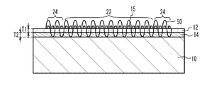
図1は、実施例1に係る弾性波共振器の斜視図、図2(a)は、実施例1における弾性波共振器の平面図、図2(b)は、図2(a)のA−A断面図である。電極指の配列方向をX方向、電極指の延伸方向をY方向、支持基板および圧電基板の積層方向をZ方向とする。X方向、Y方向およびZ方向は、圧電基板の結晶方位のX軸方向およびY軸方向とは必ずしも対応しない。 FIG. 1 is a perspective view of an elastic wave resonator according to the first embodiment, FIG. 2A is a plan view of the elastic wave resonator according to the first embodiment, and FIG. 2B is A in FIG. It is -A sectional drawing. The arrangement direction of the electrode fingers is the X direction, the extending direction of the electrode fingers is the Y direction, and the stacking direction of the support substrate and the piezoelectric substrate is the Z direction. The X direction, the Y direction, and the Z direction do not necessarily correspond to the X axis direction and the Y axis direction of the crystal orientation of the piezoelectric substrate.
図1、図2(a)および図2(b)に示すように、支持基板10上に接合膜11を介し温度補償膜14が接合されている。温度補償膜14上に圧電基板12が接合されている。圧電基板12および温度補償膜14の厚さをそれぞれT1およびT2とする。
As shown in FIGS. 1, 2 (a), and 2 (b), a
圧電基板12上に弾性波共振器20が設けられている。弾性波共振器20はIDT22および反射器24を有する。反射器24はIDT22のX方向の両側に設けられている。IDT22および反射器24は、圧電基板12上の金属膜13により形成される。
An
IDT22は、対向する一対の櫛型電極18を備える。櫛型電極18は、複数の電極指15と、複数の電極指15が接続されたバスバー16と、を備える。一対の櫛型電極18の電極指15が交差する領域が交差領域25である。交差領域25の長さが開口長である。一対の櫛型電極18は、交差領域25の少なくとも一部において電極指15がほぼ互い違いとなるように、対向して設けられている。交差領域25において複数の電極指15が励振する弾性波は、主にX方向に伝搬する。櫛型電極18の電極指15の2本分のピッチがほぼ弾性波の波長λとなる。反射器24は、IDT22の電極指15が励振した弾性波(弾性表面波)を反射する。これにより弾性波はIDT22の交差領域25内に閉じ込められる。
The IDT 22 includes a pair of
圧電基板12としては、例えば、単結晶タンタル酸リチウム(TaLiO3)基板または単結晶ニオブ酸リチウム(NbLiO3)基板であり、例えば回転YカットX伝搬タンタル酸リチウム基板または回転YカットX伝搬ニオブ酸リチウム基板である。
The
温度補償膜14は、圧電基板12の位相速度の温度係数(すなわち弾性率の温度係数)の符号と反対の符号の位相速度の温度係数を有する。例えば圧電基板12の位相速度の温度係数は負であり、温度補償膜14の位相速度の温度係数は正である。温度補償膜14は、例えば無添加または添加元素を含む酸化シリコン(SiO2)膜であり、非結晶状である。
The
支持基板10は、例えばサファイア基板、スピネル基板、シリコン基板、水晶基板、石英基板またはアルミナ基板である。サファイア基板は単結晶Al2O3基板であり、スピネル基板は単結晶もしくは多結晶MgAl2O4基板であり、シリコン基板は単結晶Si基板であり、水晶基板は単結晶SiO2基板であり、石英基板は多結晶SiO2基板であり、アルミナ基板は多結晶Al2O3基板である。支持基板10のX方向の線熱膨張係数は圧電基板12のX方向の線熱膨張係数より小さい。
The
接合膜11は、支持基板10と温度補償膜14とを接合するための層である。例えば、特許文献1に記載されているように、支持基板10の上面と温度補償膜14の下面をイオンビーム、中性ビームまたはプラズマにより活性化する。このとき、支持基板10の上面と温度補償膜14の下面とに各々アモルファス層が形成される。アモルファス層を接合することで、支持基板10の上面に温度補償膜14の下面が接合される。この場合、接合膜11の厚さは1nmから8nmである。接合膜11は厚さが1nmから100nmの絶縁膜でもよい。接合膜11は設けられていなくてもよい。温度補償膜14と圧電基板12との間に接合膜11が設けられていてもよい。
The
金属膜13は、例えばAl(アルミニウム)またはCu(銅)を主成分とする膜であり、例えばAl膜またはCu膜である。電極指15と圧電基板12との間にTi(チタン)膜またはCr(クロム)膜等の密着膜が設けられていてもよい。密着膜は電極指15より薄い。電極指15を覆うように絶縁膜が設けられていてもよい。絶縁膜は保護膜または温度補償膜として機能する。
The
[温度補償膜を設ける理由の説明]
以下、実施例1において周波数温度係数が0に近くなる理由について説明する。周波数温度係数TCFは以下の式により表される。
TCF=TCV−CTE
TCV(Temperature Coefficient of Velocity)は、音速(位相速度)の温度係数である。CTE(Coefficient of Thermal Expansion)は熱膨張係数である。圧電基板12として用いるX伝搬タンタル酸リチウム基板のX軸方向の線熱膨張係数は約16ppm/Kである。支持基板10として用いるサファイア基板のC軸(X軸に平行となる軸)の線熱膨張係数は約7.7ppm/Kである。よって、圧電基板12の厚さを小さくすると、弾性波共振器20としてのCTEは支持基板10のCTEに近づく。しかし、支持基板10のCTEより小さくはならない。
[Description of the reason for providing a temperature compensation film]
Hereinafter, the reason why the frequency temperature coefficient is close to 0 in the first embodiment will be described. The frequency temperature coefficient TCF is expressed by the following equation.
TCF = TCV-CTE
TCV (Temperature Coefficient of Velocity) is a temperature coefficient of sound velocity (phase velocity). CTE (Coefficient of Thermal Expansion) is a thermal expansion coefficient. The linear thermal expansion coefficient in the X-axis direction of the X-propagating lithium tantalate substrate used as the
一般的に線熱膨張係数は材料によらず正である。また、一般的な圧電基板12として用いられる材料ではTCVは負である。このため、TCFは負となってしまう。そこで、温度補償膜14として正のTCVを有する材料を用いる。これにより、温度補償膜14の正のTCVが圧電基板12の負のTCVおよび支持基板10の−CTEを補償する。よって、TCFを0付近にすることができる。
Generally, the linear thermal expansion coefficient is positive regardless of the material. Moreover, TCV is negative in the material used as the general
[圧電基板12と温度補償膜14の厚さの範囲の説明]
次に、圧電基板12と温度補償膜14の好ましい厚さについて説明する。図3は、実施例1に係る弾性波共振器の断面図である。図3に示すように、IDT22の電極指15は弾性波50を励振する。なお、図中の弾性波50は変位のイメージを示しており実際の弾性波の変位とは異なる。例えば圧電基板12が回転YカットX伝搬タンタル酸リチウム基板の場合、IDT22は主にSH(Shear Horizontal)波を励振する。SH波は圧電基板12の表面に平行でかつSH波の伝搬方向に直交方向に変位する波である。温度補償膜14のTCVが圧電基板12の負のTCVおよび支持基板10の−CTEを補償するには、温度補償膜14内に弾性表面波の変位が分布していることが求められる。
[Description of thickness range of
Next, preferable thicknesses of the
そこで、基板内の共振周波数における総変位分布をシミュレーションした。図4(a)および図4(b)は、シミュレーションAおよびBにおける弾性波共振器の断面図である。図4(a)に示すように、シミュレーションAでは、基板を圧電基板12である42°回転YカットX伝搬タンタル酸リチウム基板のみとし、支持基板10および温度補償膜14を設けていない。図4(b)に示すように、シミュレーションBでは、基板を支持基板10であるサファイア基板と圧電基板12である42°回転YカットX伝搬タンタル酸リチウム基板とし、温度補償膜14を設けていない。圧電基板12の厚さT1は約0.7λとした。シミュレーションAおよびBとも電極指15が接する圧電基板12の表面を0とし、基板の深さ方向を位置Zとした。
Therefore, the total displacement distribution at the resonance frequency in the substrate was simulated. 4A and 4B are cross-sectional views of the acoustic wave resonator in simulations A and B. FIG. As shown in FIG. 4A, in the simulation A, the substrate is only the 42 ° rotated Y-cut X-propagating lithium tantalate substrate that is the
図5(a)および図5(b)は、シミュレーションAおよびBにおける位置Zに対する総変位分布を示す図である。図5(a)および図5(b)の上に圧電基板12および支持基板10の範囲を示す両矢印を図示している。図5(a)に示すように、シミュレーションAでは、Z/λが2以下にほとんどの変位が収まる。特に、Z/λが1.5以下にほとんどの変位の分布が収まる。これは、弾性表面波は圧電基板12の表面から約2λ(特に1.5λ)までの範囲を伝搬することを示している。図5(b)に示すように、シミュレーションBでは、Z/λが1以下にほとんどの変位が収まる。特に支持基板10内にはほとんど変位が分布しない。これは、支持基板10の位相速度が大きいためである。
FIGS. 5A and 5B are diagrams showing the total displacement distribution with respect to the position Z in the simulations A and B. FIG. The double-headed arrows indicating the ranges of the
以上のシミュレーションのように、弾性表面波は、基板表面から2λ(特に1.5λ)以内を伝搬する。よって、実施例1において、温度補償膜14を機能させるためには、温度補償膜14は、基板表面から2λ(特に1.5λ)以内に存在することが求められる。
As in the above simulation, the surface acoustic wave propagates within 2λ (especially 1.5λ) from the substrate surface. Therefore, in the first embodiment, in order for the
次に、バルク波について説明する。図6(a)から図6(c)は、バルク波を説明する断面図である。図6(a)に示すように、基板が圧電基板12のみの場合、IDT22が圧電基板12の表面にSH波等の弾性表面波52を励振する。弾性表面波52の変位が存在する厚さT4は2λ程度である。IDT22が弾性表面波52を励振するとき、IDT22は圧電基板12内にバルク波54を放出する。バルク波54は主モードの弾性表面波52に比べて1/10の大きさである。バルク波54が存在する厚さT5は10λ程度である。バルク波54が圧電基板12内を伝搬すると弾性表面波52のエネルギーがバルク波54として失われる。よって、弾性波共振器の損失が大きくなる。
Next, the bulk wave will be described. FIG. 6A to FIG. 6C are cross-sectional views illustrating bulk waves. As shown in FIG. 6A, when the substrate is only the
図6(b)に示すように、圧電基板12の下に温度補償膜14を設け、温度補償膜14の下に支持基板10を設ける。圧電基板12の厚さT1は厚さT4より小さい。これにより、弾性表面波52の変位は圧電基板12と温度補償膜14の両方に分布する。よって、TCFを抑制できる。温度補償膜14の厚さT2が大きいと、温度補償膜14内をバルク波54が伝搬する。これにより、弾性表面波52のエネルギーがバルク波54として失われる。よって、弾性波共振器の損失が大きくなる。矢印56のように、支持基板10内にバルク波が伝搬しない。
As shown in FIG. 6B, a
図6(c)に示すように、実施例1では、温度補償膜14を薄くし、厚さT1とT2との合計の厚さを厚さT4より小さくする。支持基板10は、圧電基板12および温度補償膜14の位相速度より大きい位相速度を有する。例えば、タンタル酸リチウム、酸化シリコンおよびサファイアの速い横波の位相速度は約4211m/秒、約5840m/秒および6761m/秒である。このため、矢印56のように、支持基板10内にバルク波が伝搬しない。弾性表面波52およびバルク波54ともに圧電基板12および温度補償膜14内に閉じ込められる。よって、弾性波共振器の損失を抑制できる。また、バルク波に起因したスプリアスを抑制できる。
As shown in FIG. 6C, in Example 1, the
[実験]
実施例1と比較例1の弾性波共振器を作製した。作製条件は以下である。
実施例1
支持基板10:厚さが500μmのR面を上面とする単結晶サファイア基板
温度補償膜14:厚さT2が1μmの酸化シリコン(SiO2)膜
圧電基板12:厚さT1が1μmの42°回転YカットX伝搬タンタル酸リチウム基板
弾性波の波長λ:4μm
比較例1
支持基板10:厚さが500μmのR面を上面とする単結晶サファイア基板
温度補償膜14:なし
圧電基板12:厚さが3μmの42°回転YカットX伝搬タンタル酸リチウム基板
弾性波の波長λ:4μm
[Experiment]
The acoustic wave resonators of Example 1 and Comparative Example 1 were produced. The production conditions are as follows.
Example 1
Support substrate 10: Single crystal sapphire substrate having an R surface of 500 μm as the upper surface Temperature compensation film 14: Silicon oxide (SiO 2 ) film having a thickness T2 of 1 μm Piezoelectric substrate 12: 42 ° rotation with a thickness T1 of 1 μm Y-cut X-propagating lithium tantalate substrate Wavelength of elastic wave λ: 4 μm
Comparative Example 1
Support substrate 10: Single crystal sapphire substrate having an R surface of 500 μm as the upper surface Temperature compensation film 14: None Piezoelectric substrate 12: 42 ° rotated Y-cut X-propagation lithium tantalate substrate with a thickness of 3 μm Wavelength λ of elastic wave : 4μm
実施例1および比較例1の共振周波数のTCFを測定した。実施例1では、TCF=6ppm/K、比較例1では、TCF=−13.4ppm/Kである。 The resonance frequency TCFs of Example 1 and Comparative Example 1 were measured. In Example 1, TCF = 6 ppm / K, and in Comparative Example 1, TCF = −13.4 ppm / K.
図7は、実施例1における弾性波共振器の周波数に対するアドミッタンスを示す図である。図7に示すように、25℃と85℃においてアドミッタンス特性はほとんど変わらない。共振周波数frおよび反共振周波数faの温度依存はほとんどない。このように、温度補償膜14を設けることで、TCFを0に近づけることができる。
FIG. 7 is a diagram illustrating the admittance with respect to the frequency of the acoustic wave resonator according to the first embodiment. As shown in FIG. 7, the admittance characteristics hardly change at 25 ° C. and 85 ° C. There is almost no temperature dependence of the resonance frequency fr and the antiresonance frequency fa. Thus, by providing the
[実施例1の製造方法]
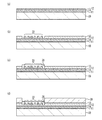
実施例1に係る弾性波共振器の製造方法について説明する。図8(a)から図10(b)は、実施例1に係る弾性波共振器の製造方法を示す断面図である。図8(a)に示すように、圧電基板12を準備する。図8(b)に示すように、圧電基板12上に温度補償膜14をスパッタリング法、真空蒸着法またはCVD(Chemical Vapor Deposition)法を用い形成する。図8(c)に示すように、温度補償膜14上に接合膜11をスパッタリング法、真空蒸着法またはCVD法を用い形成する。接合膜11は、例えばシリコン膜、酸化アルミニウム膜または窒化アルミニウム膜である。図8(d)に示すように、支持基板10の上面および接合膜11の下面を活性化する。活性化の方法は例えば特許文献1と同じである。図8(e)に示すように、支持基板10と接合膜11とを常温において接合する。
[Production Method of Example 1]
A method for manufacturing the acoustic wave resonator according to the first embodiment will be described. FIGS. 8A to 10B are cross-sectional views illustrating the method for manufacturing the acoustic wave resonator according to the first embodiment. As shown in FIG. 8A, the
図9(a)に示すように、圧電基板12の上面を例えばCMP(Chemical Mechanical Polishing)法を用い薄膜化する。図9(b)に示すように、圧電基板12の上面に金属膜13を形成する。金属膜13により弾性波共振器20が形成される。図9(c)に示すように、弾性波共振器20を覆うように保護膜26を形成する。保護膜26は例えば窒化シリコン膜または酸化シリコン膜等の絶縁膜である。図9(d)に示すように、金属膜13上に配線層28を形成する。配線層28は、例えば銅層または金層である。個片化することにより、チップを形成する。
As shown in FIG. 9A, the upper surface of the
図10(a)に示すように、チップ45では、圧電基板12下に弾性波共振器20およびパッド32が設けられ、パッド32下にバンプ30が設けられている。パッド32は、例えば図9(d)の配線層の一部である。バンプ30は例えば金バンプまたは半田バンプである。保護膜26の図示は省略している。パッケージ基板40上にパッド42が設けられ、パッケージ基板40下に端子44が設けられている。バンプ30をパッド42に接合させる。図10(b)に示すように、パッケージ基板40上にチップ45を覆うよう封止部48を形成する。封止部48は、例えば樹脂等の絶縁体または半田等の金属である。封止部48は、弾性波共振器20を空隙43に封止する。これにより弾性波デバイスが製造できる。
As shown in FIG. 10A, in the
実施例1によれば、圧電基板12は、支持基板10上に設けられ、支持基板10の位相速度より小さい位相速度を有する。温度補償膜14は、支持基板10と圧電基板12との間に設けられ、支持基板10の位相速度より小さい位相速度と、圧電基板12の位相速度の温度係数(TCV)の符号と逆の符号の位相速度の温度係数(TCV)と、を有する。一対の櫛型電極18は、圧電基板12上に設けられ、各々複数の電極指15を備え、一方の櫛型電極の電極指15の平均ピッチが温度補償膜14と圧電基板12の合計の厚さ(T1+T2)の1/2以上である。
According to the first embodiment, the
温度補償膜14のTCVの符号を圧電基板12のTCVの符号と逆とする。これにより、図3において説明したようにTCFを抑制できる。電極指15の平均ピッチ(弾性波の波長λにほぼ相当する)を厚さT1+T2の1/2以上とする。これにより、図5(a)および図5(b)のように、弾性波は圧電基板12および温度補償膜14を伝搬するため、TCFを抑制できる。よって、周波数温度特性を向上できる。さらに、図6(a)から図6(c)において説明したように、バルク波に起因する損失を抑制できる。
The sign of TCV of the
電極指15の平均ピッチは、弾性波共振器20のX方向の長さを電極指15の対数(電極指15の本数の1/2)で除することにより算出できる。電極指15の平均ピッチは、温度補償膜14と圧電基板12の合計の厚さ(T1+T2)の1/1.5倍以上が好ましく、1/1.2倍以上がより好ましく、1以上がさらに好ましい。弾性表面波を圧電基板12および温度補償膜14内を伝搬させるため、電極指15の平均ピッチは、厚さ(T1+T2)の1/0.1倍以下が好ましく、1/0.2倍以下がより好ましく、1倍以下がさらに好ましい。
The average pitch of the
電極指15の平均ピッチは圧電基板12の厚さT1より大きい。これにより、図5(a)および図5(b)のように、弾性表面波の変位分布を温度補償膜14内により存在させることができる。電極指15の平均ピッチは圧電基板12の厚さT1の1/0.8倍以上が好ましく、1/0.6倍以上がより好ましく、1/0.5倍以上がさらに好ましい。弾性表面波を圧電基板12内を伝搬させるため、電極指15の平均ピッチは圧電基板12の厚さT1の1/0.1倍以下が好ましく、1/0.2倍以下がより好ましく、1/0.3倍以下がさらに好ましい。
The average pitch of the
複数の電極指15の配列方向における支持基板10の線熱膨張係数は、配列方向における圧電基板12の線熱膨張係数より小さい。これにより、CTEを小さくできる。
The linear thermal expansion coefficient of the
TCFを抑制するため、圧電基板12の厚さT1のT1+T2に対する比は、0.1以上かつ0.9以下が好ましく、0.2以上かつ0.8以下がより好ましく、0.3以上かつ0.7以下がさらに好ましい。図7の実験のように、厚さT1とT2とはT1/(T1+T2)が0.4以上かつ0.6以下となる程度に略等しいことが好ましい。
In order to suppress TCF, the ratio of the thickness T1 of the
圧電基板12は、タンタル酸リチウム基板またはニオブ酸リチウム基板である。支持基板10は、サファイア基板、スピネル基板、シリコン基板、水晶基板、石英基板、またはアルミナ基板でありかつ単結晶基板または多結晶基板である。温度補償膜14は酸化シリコン膜である。これにより、周波数温度特性を向上できかつ損失を抑制できる。
The
図3において説明したように、一対の櫛型電極18が弾性表面波(特にSH波)を励振する場合、バルク波が生成されやすい。よって、弾性表面波がSH波であるとき、T1+T2を1.5λ以下とすることが好ましい。弾性表面波をSH波とするため、圧電基板12は、20°から48°回転YカットX伝搬タンタル酸リチウム基板であることが好ましい。
As described in FIG. 3, when the pair of comb-shaped
図11(a)は、実施例2に係るフィルタの回路図である。図11(a)に示すように、入力端子Tinと出力端子Toutとの間に、1または複数の直列共振器S1からS3が直列に接続されている。入力端子Tinと出力端子Toutとの間に、1または複数の並列共振器P1およびP2が並列に接続されている。1または複数の直列共振器S1からS3および1または複数の並列共振器P1およびP2の少なくとも1つに実施例1の弾性波共振器を用いることができる。ラダー型フィルタの共振器の個数等は適宜設定できる。 FIG. 11A is a circuit diagram of a filter according to the second embodiment. As shown in FIG. 11A, one or more series resonators S1 to S3 are connected in series between the input terminal Tin and the output terminal Tout. One or more parallel resonators P1 and P2 are connected in parallel between the input terminal Tin and the output terminal Tout. The elastic wave resonator of the first embodiment can be used for at least one of the one or more series resonators S1 to S3 and the one or more parallel resonators P1 and P2. The number of resonators of the ladder type filter can be set as appropriate.
[実施例2の変形例1]
図11(b)は、実施例2の変形例1に係るフィルタを示す平面図である。図11(b)に示すように、多重モード型フィルタDMSは、IDT22aから22cおよび反射器24を有している。IDT22aから22cおよび反射器24は圧電基板12上に設けられている。IDT22aから22cは弾性表面波の伝搬方向に配列されている。IDT22aから22cの外側に反射器24が設けられている。IDT22bの一端は入力端子Tinに接続され、他端はグランド端子に接続されている。IDT22aの一端およびIDT22cの一端は共通に出力端子Toutに接続されている。IDT22aの他端およびIDT22cの他端はグランド端子に接続されている。多重モード型フィルタDMSに実施例1の弾性波共振器の構造を用いることができる。
[
FIG. 11B is a plan view illustrating a filter according to the first modification of the second embodiment. As shown in FIG. 11B, the multimode filter DMS includes IDTs 22a to 22c and a
[実施例2の変形例2]
図11(c)は、実施例2の変形例2に係るデュプレクサの回路図である。図11(c)に示すように、共通端子Antと送信端子Txとの間に送信フィルタ46が接続されている。共通端子Antと受信端子Rxとの間に受信フィルタ47が接続されている。送信フィルタ46は、送信端子Txから入力された高周波信号のうち送信帯域の信号を送信信号として共通端子Antに通過させ、他の周波数の信号を抑圧する。受信フィルタ47は、共通端子Antから入力された高周波信号のうち受信帯域の信号を受信信号として受信端子Rxに通過させ、他の周波数の信号を抑圧する。送信フィルタ46および受信フィルタ47の少なくとも一方を実施例2およびその変形例1のフィルタとすることができる。
[
FIG. 11C is a circuit diagram of a duplexer according to the second modification of the second embodiment. As shown in FIG. 11C, a
マルチプレクサとしてデュプレクサを例に説明したがトリプレクサまたはクワッドプレクサでもよい。 Although the duplexer has been described as an example of the multiplexer, a triplexer or a quadplexer may be used.
以上、本発明の実施例について詳述したが、本発明はかかる特定の実施例に限定されるものではなく、特許請求の範囲に記載された本発明の要旨の範囲内において、種々の変形・変更が可能である。 Although the embodiments of the present invention have been described in detail above, the present invention is not limited to such specific embodiments, and various modifications and changes can be made within the scope of the gist of the present invention described in the claims. It can be changed.
10 支持基板
11 接合膜
12 圧電基板
14 温度補償膜
15 電極指
18 櫛型電極
20 弾性波共振器
22 IDT
DESCRIPTION OF
Claims (9)
前記支持基板上に設けられ、前記支持基板の位相速度より小さい位相速度を有する圧電基板と、
前記支持基板と前記圧電基板との間に設けられ、前記支持基板の位相速度より小さい位相速度と、前記圧電基板の位相速度の温度係数の符号と逆の符号の位相速度の温度係数と、を有する温度補償膜と、
前記圧電基板上に設けられ、各々複数の電極指を備え、一方の櫛型電極の電極指の平均ピッチが前記温度補償膜と前記圧電基板の合計の厚さの1/2以上である一対の櫛型電極と、
を備える弾性波共振器。 A support substrate;
A piezoelectric substrate provided on the support substrate and having a phase velocity smaller than the phase velocity of the support substrate;
A phase velocity that is provided between the support substrate and the piezoelectric substrate and that is smaller than the phase velocity of the support substrate, and a temperature coefficient of a phase velocity that is opposite to the sign of the temperature coefficient of the phase velocity of the piezoelectric substrate; A temperature compensation film having,
A pair of electrode fingers provided on the piezoelectric substrate, each having a plurality of electrode fingers, wherein an average pitch of the electrode fingers of one comb-shaped electrode is ½ or more of a total thickness of the temperature compensation film and the piezoelectric substrate A comb electrode;
An elastic wave resonator comprising:
前記支持基板は、サファイア基板、スピネル基板、シリコン基板、水晶基板、石英基板、またはアルミナ基板でありかつ単結晶基板または多結晶基板であり、
前記温度補償膜は酸化シリコン膜である請求項1から4のいずれか一項に記載の弾性波共振器。 The piezoelectric substrate is a lithium tantalate substrate or a lithium niobate substrate,
The support substrate is a sapphire substrate, a spinel substrate, a silicon substrate, a quartz substrate, a quartz substrate, or an alumina substrate, and is a single crystal substrate or a polycrystalline substrate,
The acoustic wave resonator according to claim 1, wherein the temperature compensation film is a silicon oxide film.
Priority Applications (2)
| Application Number | Priority Date | Filing Date | Title |
|---|---|---|---|
| JP2018095422A JP2019201345A (en) | 2018-05-17 | 2018-05-17 | Acoustic wave resonator, filter and multiplexer |
| US16/375,512 US11595019B2 (en) | 2018-04-20 | 2019-04-04 | Acoustic wave resonator, filter, and multiplexer |
Applications Claiming Priority (1)
| Application Number | Priority Date | Filing Date | Title |
|---|---|---|---|
| JP2018095422A JP2019201345A (en) | 2018-05-17 | 2018-05-17 | Acoustic wave resonator, filter and multiplexer |
Publications (1)
| Publication Number | Publication Date |
|---|---|
| JP2019201345A true JP2019201345A (en) | 2019-11-21 |
Family
ID=68613281
Family Applications (1)
| Application Number | Title | Priority Date | Filing Date |
|---|---|---|---|
| JP2018095422A Pending JP2019201345A (en) | 2018-04-20 | 2018-05-17 | Acoustic wave resonator, filter and multiplexer |
Country Status (1)
| Country | Link |
|---|---|
| JP (1) | JP2019201345A (en) |
Cited By (5)
| Publication number | Priority date | Publication date | Assignee | Title |
|---|---|---|---|---|
| CN112929004A (en) * | 2019-12-06 | 2021-06-08 | 太阳诱电株式会社 | Acoustic wave resonator, filter, multiplexer and wafer |
| CN113395054A (en) * | 2020-03-13 | 2021-09-14 | 太阳诱电株式会社 | Acoustic wave device, filter and multiplexer |
| CN116722838A (en) * | 2023-06-29 | 2023-09-08 | 北京超材信息科技有限公司 | Surface acoustic wave filter, surface acoustic wave filter set, multiplexer and radio frequency module |
| US11916531B2 (en) | 2020-07-29 | 2024-02-27 | Taiyo Yuden Co., Ltd. | Acoustic wave device, filter, and multiplexer |
| US11962282B2 (en) | 2020-06-17 | 2024-04-16 | Taiyo Yuden Co., Ltd. | Acoustic wave device, filter, and multiplexer |
Citations (4)
| Publication number | Priority date | Publication date | Assignee | Title |
|---|---|---|---|---|
| JP2004343359A (en) * | 2003-05-14 | 2004-12-02 | Fujitsu Media Device Kk | Method of manufacturing surface acoustic wave element |
| WO2011046117A1 (en) * | 2009-10-13 | 2011-04-21 | 株式会社村田製作所 | Elastic surface-wave device |
| WO2012086639A1 (en) * | 2010-12-24 | 2012-06-28 | 株式会社村田製作所 | Elastic wave device and production method thereof |
| JP2018074575A (en) * | 2016-10-20 | 2018-05-10 | スカイワークス ソリューションズ, インコーポレイテッドSkyworks Solutions, Inc. | Elastic wave device with sub-wavelength thick piezoelectric layer |
-
2018
- 2018-05-17 JP JP2018095422A patent/JP2019201345A/en active Pending
Patent Citations (4)
| Publication number | Priority date | Publication date | Assignee | Title |
|---|---|---|---|---|
| JP2004343359A (en) * | 2003-05-14 | 2004-12-02 | Fujitsu Media Device Kk | Method of manufacturing surface acoustic wave element |
| WO2011046117A1 (en) * | 2009-10-13 | 2011-04-21 | 株式会社村田製作所 | Elastic surface-wave device |
| WO2012086639A1 (en) * | 2010-12-24 | 2012-06-28 | 株式会社村田製作所 | Elastic wave device and production method thereof |
| JP2018074575A (en) * | 2016-10-20 | 2018-05-10 | スカイワークス ソリューションズ, インコーポレイテッドSkyworks Solutions, Inc. | Elastic wave device with sub-wavelength thick piezoelectric layer |
Cited By (8)
| Publication number | Priority date | Publication date | Assignee | Title |
|---|---|---|---|---|
| CN112929004A (en) * | 2019-12-06 | 2021-06-08 | 太阳诱电株式会社 | Acoustic wave resonator, filter, multiplexer and wafer |
| JP2021093570A (en) * | 2019-12-06 | 2021-06-17 | 太陽誘電株式会社 | Surface acoustic wave resonator, filter, and multiplexer |
| JP7433873B2 (en) | 2019-12-06 | 2024-02-20 | 太陽誘電株式会社 | Acoustic wave resonators, filters, and multiplexers |
| CN113395054A (en) * | 2020-03-13 | 2021-09-14 | 太阳诱电株式会社 | Acoustic wave device, filter and multiplexer |
| US11962282B2 (en) | 2020-06-17 | 2024-04-16 | Taiyo Yuden Co., Ltd. | Acoustic wave device, filter, and multiplexer |
| US11916531B2 (en) | 2020-07-29 | 2024-02-27 | Taiyo Yuden Co., Ltd. | Acoustic wave device, filter, and multiplexer |
| CN116722838A (en) * | 2023-06-29 | 2023-09-08 | 北京超材信息科技有限公司 | Surface acoustic wave filter, surface acoustic wave filter set, multiplexer and radio frequency module |
| CN116722838B (en) * | 2023-06-29 | 2024-08-02 | 北京超材信息科技有限公司 | Surface acoustic wave filter, surface acoustic wave filter set, multiplexer and radio frequency module |
Similar Documents
| Publication | Publication Date | Title |
|---|---|---|
| JP6856825B2 (en) | Elastic wave device, demultiplexer and communication device | |
| US11595019B2 (en) | Acoustic wave resonator, filter, and multiplexer | |
| US9276558B2 (en) | Surface acoustic wave device including a confinement layer | |
| JP4917396B2 (en) | Filters and duplexers | |
| JPWO2019138810A1 (en) | Elastic wave device, multiplexer, high frequency front end circuit and communication device | |
| JP7433873B2 (en) | Acoustic wave resonators, filters, and multiplexers | |
| CN107204750B (en) | Acoustic wave device | |
| JP7278305B2 (en) | Acoustic wave device, branching filter and communication device | |
| JP2019201345A (en) | Acoustic wave resonator, filter and multiplexer | |
| WO2018070369A1 (en) | Acoustic wave device | |
| JP2018182460A (en) | Acoustic wave resonator, filter, and multiplexer | |
| JP2023060058A (en) | Acoustic wave resonator, filter and multiplexer | |
| JP6935220B2 (en) | Elastic wave elements, filters and multiplexers | |
| JP2020182130A (en) | Filter and multiplexer | |
| JPWO2019082806A1 (en) | Elastic wave element | |
| JP2014160888A (en) | Acoustic wave resonator, acoustic wave filter using the same and antenna duplexer | |
| WO2018117060A1 (en) | Acoustic wave resonator, filter device, and multiplexer | |
| JP2022176790A (en) | Elastic wave device, wafer, filter and multiplexer | |
| JP7441010B2 (en) | Acoustic wave devices, filters and multiplexers | |
| JP2022176856A (en) | Ladder filter and multiplexer | |
| JP7344662B2 (en) | multiplexer | |
| JP6886264B2 (en) | Elastic wave devices and composite substrates and their manufacturing methods | |
| JP7509598B2 (en) | Acoustic Wave Devices, Filters and Multiplexers | |
| US20230006649A1 (en) | Filter and multiplexer | |
| JP2023124332A (en) | Acoustic wave device, filter and multiplexer |
Legal Events
| Date | Code | Title | Description |
|---|---|---|---|
| A621 | Written request for application examination |
Free format text: JAPANESE INTERMEDIATE CODE: A621 Effective date: 20210107 |
|
| A977 | Report on retrieval |
Free format text: JAPANESE INTERMEDIATE CODE: A971007 Effective date: 20210921 |
|
| A131 | Notification of reasons for refusal |
Free format text: JAPANESE INTERMEDIATE CODE: A131 Effective date: 20211005 |
|
| A02 | Decision of refusal |
Free format text: JAPANESE INTERMEDIATE CODE: A02 Effective date: 20220405 |