WO2012086639A1 - Elastic wave device and production method thereof - Google Patents
Elastic wave device and production method thereof Download PDFInfo
- Publication number
- WO2012086639A1 WO2012086639A1 PCT/JP2011/079496 JP2011079496W WO2012086639A1 WO 2012086639 A1 WO2012086639 A1 WO 2012086639A1 JP 2011079496 W JP2011079496 W JP 2011079496W WO 2012086639 A1 WO2012086639 A1 WO 2012086639A1
- Authority
- WO
- WIPO (PCT)
- Prior art keywords
- film
- piezoelectric
- sound velocity
- low
- velocity
- Prior art date
Links
- 238000004519 manufacturing process Methods 0.000 title claims description 21
- 239000000758 substrate Substances 0.000 claims abstract description 104
- 230000001902 propagating effect Effects 0.000 claims abstract description 40
- 238000010897 surface acoustic wave method Methods 0.000 claims description 110
- VYPSYNLAJGMNEJ-UHFFFAOYSA-N Silicium dioxide Chemical compound O=[Si]=O VYPSYNLAJGMNEJ-UHFFFAOYSA-N 0.000 claims description 50
- 229910052814 silicon oxide Inorganic materials 0.000 claims description 49
- 238000000034 method Methods 0.000 claims description 20
- 150000002500 ions Chemical class 0.000 claims description 16
- 238000010438 heat treatment Methods 0.000 claims description 9
- 238000005468 ion implantation Methods 0.000 claims description 9
- 239000013078 crystal Substances 0.000 claims description 6
- WSMQKESQZFQMFW-UHFFFAOYSA-N 5-methyl-pyrazole-3-carboxylic acid Chemical compound CC1=CC(C(O)=O)=NN1 WSMQKESQZFQMFW-UHFFFAOYSA-N 0.000 claims description 4
- 230000008569 process Effects 0.000 claims description 2
- 239000010408 film Substances 0.000 description 430
- 230000000052 comparative effect Effects 0.000 description 41
- 230000008878 coupling Effects 0.000 description 35
- 238000010168 coupling process Methods 0.000 description 35
- 238000005859 coupling reaction Methods 0.000 description 35
- 239000010410 layer Substances 0.000 description 33
- 239000000463 material Substances 0.000 description 30
- 238000010586 diagram Methods 0.000 description 27
- 230000000694 effects Effects 0.000 description 17
- 229910004298 SiO 2 Inorganic materials 0.000 description 13
- PMHQVHHXPFUNSP-UHFFFAOYSA-M copper(1+);methylsulfanylmethane;bromide Chemical compound Br[Cu].CSC PMHQVHHXPFUNSP-UHFFFAOYSA-M 0.000 description 13
- 229910052751 metal Inorganic materials 0.000 description 9
- 239000002184 metal Substances 0.000 description 9
- 238000004088 simulation Methods 0.000 description 9
- 239000012528 membrane Substances 0.000 description 7
- 239000011521 glass Substances 0.000 description 6
- 229910052581 Si3N4 Inorganic materials 0.000 description 5
- TWNQGVIAIRXVLR-UHFFFAOYSA-N oxo(oxoalumanyloxy)alumane Chemical compound O=[Al]O[Al]=O TWNQGVIAIRXVLR-UHFFFAOYSA-N 0.000 description 5
- PNEYBMLMFCGWSK-UHFFFAOYSA-N aluminium oxide Inorganic materials [O-2].[O-2].[O-2].[Al+3].[Al+3] PNEYBMLMFCGWSK-UHFFFAOYSA-N 0.000 description 4
- 238000013461 design Methods 0.000 description 4
- 239000004065 semiconductor Substances 0.000 description 4
- HQVNEWCFYHHQES-UHFFFAOYSA-N silicon nitride Chemical compound N12[Si]34N5[Si]62N3[Si]51N64 HQVNEWCFYHHQES-UHFFFAOYSA-N 0.000 description 4
- 239000010409 thin film Substances 0.000 description 4
- 229910013641 LiNbO 3 Inorganic materials 0.000 description 3
- XUIMIQQOPSSXEZ-UHFFFAOYSA-N Silicon Chemical compound [Si] XUIMIQQOPSSXEZ-UHFFFAOYSA-N 0.000 description 3
- 230000008859 change Effects 0.000 description 3
- 239000010432 diamond Substances 0.000 description 3
- 229910003460 diamond Inorganic materials 0.000 description 3
- 238000005304 joining Methods 0.000 description 3
- 230000007246 mechanism Effects 0.000 description 3
- 239000010703 silicon Substances 0.000 description 3
- CPLXHLVBOLITMK-UHFFFAOYSA-N Magnesium oxide Chemical compound [Mg]=O CPLXHLVBOLITMK-UHFFFAOYSA-N 0.000 description 2
- MCMNRKCIXSYSNV-UHFFFAOYSA-N Zirconium dioxide Chemical compound O=[Zr]=O MCMNRKCIXSYSNV-UHFFFAOYSA-N 0.000 description 2
- 239000012790 adhesive layer Substances 0.000 description 2
- 229910045601 alloy Inorganic materials 0.000 description 2
- 239000000956 alloy Substances 0.000 description 2
- 239000000919 ceramic Substances 0.000 description 2
- 239000003989 dielectric material Substances 0.000 description 2
- 238000009792 diffusion process Methods 0.000 description 2
- 239000001257 hydrogen Substances 0.000 description 2
- 229910052739 hydrogen Inorganic materials 0.000 description 2
- 238000003780 insertion Methods 0.000 description 2
- 230000037431 insertion Effects 0.000 description 2
- 238000010030 laminating Methods 0.000 description 2
- 150000002739 metals Chemical class 0.000 description 2
- 239000011347 resin Substances 0.000 description 2
- 229920005989 resin Polymers 0.000 description 2
- 238000000926 separation method Methods 0.000 description 2
- 229910052710 silicon Inorganic materials 0.000 description 2
- HBMJWWWQQXIZIP-UHFFFAOYSA-N silicon carbide Chemical compound [Si+]#[C-] HBMJWWWQQXIZIP-UHFFFAOYSA-N 0.000 description 2
- 229910010271 silicon carbide Inorganic materials 0.000 description 2
- -1 steatite Chemical compound 0.000 description 2
- 238000012546 transfer Methods 0.000 description 2
- ZOXJGFHDIHLPTG-UHFFFAOYSA-N Boron Chemical compound [B] ZOXJGFHDIHLPTG-UHFFFAOYSA-N 0.000 description 1
- OKTJSMMVPCPJKN-UHFFFAOYSA-N Carbon Chemical compound [C] OKTJSMMVPCPJKN-UHFFFAOYSA-N 0.000 description 1
- PXGOKWXKJXAPGV-UHFFFAOYSA-N Fluorine Chemical compound FF PXGOKWXKJXAPGV-UHFFFAOYSA-N 0.000 description 1
- 229910002601 GaN Inorganic materials 0.000 description 1
- JMASRVWKEDWRBT-UHFFFAOYSA-N Gallium nitride Chemical compound [Ga]#N JMASRVWKEDWRBT-UHFFFAOYSA-N 0.000 description 1
- 230000004913 activation Effects 0.000 description 1
- 229910052782 aluminium Inorganic materials 0.000 description 1
- 125000004429 atom Chemical group 0.000 description 1
- 230000015572 biosynthetic process Effects 0.000 description 1
- 229910052796 boron Inorganic materials 0.000 description 1
- 229910052799 carbon Inorganic materials 0.000 description 1
- 229910052804 chromium Inorganic materials 0.000 description 1
- VNNRSPGTAMTISX-UHFFFAOYSA-N chromium nickel Chemical compound [Cr].[Ni] VNNRSPGTAMTISX-UHFFFAOYSA-N 0.000 description 1
- 150000001875 compounds Chemical class 0.000 description 1
- 229910052802 copper Inorganic materials 0.000 description 1
- 229910052878 cordierite Inorganic materials 0.000 description 1
- 230000003247 decreasing effect Effects 0.000 description 1
- JSKIRARMQDRGJZ-UHFFFAOYSA-N dimagnesium dioxido-bis[(1-oxido-3-oxo-2,4,6,8,9-pentaoxa-1,3-disila-5,7-dialuminabicyclo[3.3.1]nonan-7-yl)oxy]silane Chemical compound [Mg++].[Mg++].[O-][Si]([O-])(O[Al]1O[Al]2O[Si](=O)O[Si]([O-])(O1)O2)O[Al]1O[Al]2O[Si](=O)O[Si]([O-])(O1)O2 JSKIRARMQDRGJZ-UHFFFAOYSA-N 0.000 description 1
- KZHJGOXRZJKJNY-UHFFFAOYSA-N dioxosilane;oxo(oxoalumanyloxy)alumane Chemical compound O=[Si]=O.O=[Si]=O.O=[Al]O[Al]=O.O=[Al]O[Al]=O.O=[Al]O[Al]=O KZHJGOXRZJKJNY-UHFFFAOYSA-N 0.000 description 1
- 238000006073 displacement reaction Methods 0.000 description 1
- 238000009826 distribution Methods 0.000 description 1
- 238000005516 engineering process Methods 0.000 description 1
- 229910052731 fluorine Inorganic materials 0.000 description 1
- 239000011737 fluorine Substances 0.000 description 1
- 229910052839 forsterite Inorganic materials 0.000 description 1
- 229910052737 gold Inorganic materials 0.000 description 1
- 239000001307 helium Substances 0.000 description 1
- 229910052734 helium Inorganic materials 0.000 description 1
- SWQJXJOGLNCZEY-UHFFFAOYSA-N helium atom Chemical compound [He] SWQJXJOGLNCZEY-UHFFFAOYSA-N 0.000 description 1
- 125000004435 hydrogen atom Chemical class [H]* 0.000 description 1
- 230000006872 improvement Effects 0.000 description 1
- GQYHUHYESMUTHG-UHFFFAOYSA-N lithium niobate Chemical compound [Li+].[O-][Nb](=O)=O GQYHUHYESMUTHG-UHFFFAOYSA-N 0.000 description 1
- HCWCAKKEBCNQJP-UHFFFAOYSA-N magnesium orthosilicate Chemical compound [Mg+2].[Mg+2].[O-][Si]([O-])([O-])[O-] HCWCAKKEBCNQJP-UHFFFAOYSA-N 0.000 description 1
- 239000000395 magnesium oxide Substances 0.000 description 1
- 238000005259 measurement Methods 0.000 description 1
- 239000007769 metal material Substances 0.000 description 1
- 239000000203 mixture Substances 0.000 description 1
- 229910052750 molybdenum Inorganic materials 0.000 description 1
- 229910052863 mullite Inorganic materials 0.000 description 1
- 229910001120 nichrome Inorganic materials 0.000 description 1
- 229910052759 nickel Inorganic materials 0.000 description 1
- BPUBBGLMJRNUCC-UHFFFAOYSA-N oxygen(2-);tantalum(5+) Chemical compound [O-2].[O-2].[O-2].[O-2].[O-2].[Ta+5].[Ta+5] BPUBBGLMJRNUCC-UHFFFAOYSA-N 0.000 description 1
- 238000007747 plating Methods 0.000 description 1
- 229910052697 platinum Inorganic materials 0.000 description 1
- 238000005498 polishing Methods 0.000 description 1
- 238000012545 processing Methods 0.000 description 1
- 239000010453 quartz Substances 0.000 description 1
- 230000009467 reduction Effects 0.000 description 1
- 229910052594 sapphire Inorganic materials 0.000 description 1
- 239000010980 sapphire Substances 0.000 description 1
- 229910052709 silver Inorganic materials 0.000 description 1
- 238000004544 sputter deposition Methods 0.000 description 1
- 229910001936 tantalum oxide Inorganic materials 0.000 description 1
- 229910052719 titanium Inorganic materials 0.000 description 1
- 229910052721 tungsten Inorganic materials 0.000 description 1
- 238000007740 vapor deposition Methods 0.000 description 1
Images


Classifications
-
- H—ELECTRICITY
- H03—ELECTRONIC CIRCUITRY
- H03H—IMPEDANCE NETWORKS, e.g. RESONANT CIRCUITS; RESONATORS
- H03H9/00—Networks comprising electromechanical or electro-acoustic devices; Electromechanical resonators
- H03H9/02—Details
- H03H9/125—Driving means, e.g. electrodes, coils
- H03H9/145—Driving means, e.g. electrodes, coils for networks using surface acoustic waves
-
- H—ELECTRICITY
- H03—ELECTRONIC CIRCUITRY
- H03H—IMPEDANCE NETWORKS, e.g. RESONANT CIRCUITS; RESONATORS
- H03H3/00—Apparatus or processes specially adapted for the manufacture of impedance networks, resonating circuits, resonators
- H03H3/007—Apparatus or processes specially adapted for the manufacture of impedance networks, resonating circuits, resonators for the manufacture of electromechanical resonators or networks
- H03H3/08—Apparatus or processes specially adapted for the manufacture of impedance networks, resonating circuits, resonators for the manufacture of electromechanical resonators or networks for the manufacture of resonators or networks using surface acoustic waves
- H03H3/10—Apparatus or processes specially adapted for the manufacture of impedance networks, resonating circuits, resonators for the manufacture of electromechanical resonators or networks for the manufacture of resonators or networks using surface acoustic waves for obtaining desired frequency or temperature coefficient
-
- H—ELECTRICITY
- H03—ELECTRONIC CIRCUITRY
- H03H—IMPEDANCE NETWORKS, e.g. RESONANT CIRCUITS; RESONATORS
- H03H9/00—Networks comprising electromechanical or electro-acoustic devices; Electromechanical resonators
- H03H9/02—Details
- H03H9/0222—Details of interface-acoustic, boundary, pseudo-acoustic or Stonely wave devices
-
- H—ELECTRICITY
- H03—ELECTRONIC CIRCUITRY
- H03H—IMPEDANCE NETWORKS, e.g. RESONANT CIRCUITS; RESONATORS
- H03H3/00—Apparatus or processes specially adapted for the manufacture of impedance networks, resonating circuits, resonators
- H03H3/007—Apparatus or processes specially adapted for the manufacture of impedance networks, resonating circuits, resonators for the manufacture of electromechanical resonators or networks
- H03H3/02—Apparatus or processes specially adapted for the manufacture of impedance networks, resonating circuits, resonators for the manufacture of electromechanical resonators or networks for the manufacture of piezoelectric or electrostrictive resonators or networks
- H03H3/04—Apparatus or processes specially adapted for the manufacture of impedance networks, resonating circuits, resonators for the manufacture of electromechanical resonators or networks for the manufacture of piezoelectric or electrostrictive resonators or networks for obtaining desired frequency or temperature coefficient
-
- H—ELECTRICITY
- H03—ELECTRONIC CIRCUITRY
- H03H—IMPEDANCE NETWORKS, e.g. RESONANT CIRCUITS; RESONATORS
- H03H3/00—Apparatus or processes specially adapted for the manufacture of impedance networks, resonating circuits, resonators
- H03H3/007—Apparatus or processes specially adapted for the manufacture of impedance networks, resonating circuits, resonators for the manufacture of electromechanical resonators or networks
- H03H3/08—Apparatus or processes specially adapted for the manufacture of impedance networks, resonating circuits, resonators for the manufacture of electromechanical resonators or networks for the manufacture of resonators or networks using surface acoustic waves
-
- H—ELECTRICITY
- H03—ELECTRONIC CIRCUITRY
- H03H—IMPEDANCE NETWORKS, e.g. RESONANT CIRCUITS; RESONATORS
- H03H9/00—Networks comprising electromechanical or electro-acoustic devices; Electromechanical resonators
- H03H9/02—Details
- H03H9/02535—Details of surface acoustic wave devices
- H03H9/02543—Characteristics of substrate, e.g. cutting angles
- H03H9/02574—Characteristics of substrate, e.g. cutting angles of combined substrates, multilayered substrates, piezoelectrical layers on not-piezoelectrical substrate
-
- H—ELECTRICITY
- H03—ELECTRONIC CIRCUITRY
- H03H—IMPEDANCE NETWORKS, e.g. RESONANT CIRCUITS; RESONATORS
- H03H9/00—Networks comprising electromechanical or electro-acoustic devices; Electromechanical resonators
- H03H9/02—Details
- H03H9/02535—Details of surface acoustic wave devices
- H03H9/02818—Means for compensation or elimination of undesirable effects
- H03H9/02834—Means for compensation or elimination of undesirable effects of temperature influence
-
- H—ELECTRICITY
- H03—ELECTRONIC CIRCUITRY
- H03H—IMPEDANCE NETWORKS, e.g. RESONANT CIRCUITS; RESONATORS
- H03H9/00—Networks comprising electromechanical or electro-acoustic devices; Electromechanical resonators
- H03H9/25—Constructional features of resonators using surface acoustic waves
-
- H—ELECTRICITY
- H03—ELECTRONIC CIRCUITRY
- H03H—IMPEDANCE NETWORKS, e.g. RESONANT CIRCUITS; RESONATORS
- H03H9/00—Networks comprising electromechanical or electro-acoustic devices; Electromechanical resonators
- H03H9/46—Filters
- H03H9/54—Filters comprising resonators of piezoelectric or electrostrictive material
-
- H—ELECTRICITY
- H10—SEMICONDUCTOR DEVICES; ELECTRIC SOLID-STATE DEVICES NOT OTHERWISE PROVIDED FOR
- H10N—ELECTRIC SOLID-STATE DEVICES NOT OTHERWISE PROVIDED FOR
- H10N30/00—Piezoelectric or electrostrictive devices
- H10N30/01—Manufacture or treatment
-
- H—ELECTRICITY
- H10—SEMICONDUCTOR DEVICES; ELECTRIC SOLID-STATE DEVICES NOT OTHERWISE PROVIDED FOR
- H10N—ELECTRIC SOLID-STATE DEVICES NOT OTHERWISE PROVIDED FOR
- H10N30/00—Piezoelectric or electrostrictive devices
- H10N30/80—Constructional details
- H10N30/87—Electrodes or interconnections, e.g. leads or terminals
- H10N30/877—Conductive materials
-
- H—ELECTRICITY
- H03—ELECTRONIC CIRCUITRY
- H03H—IMPEDANCE NETWORKS, e.g. RESONANT CIRCUITS; RESONATORS
- H03H3/00—Apparatus or processes specially adapted for the manufacture of impedance networks, resonating circuits, resonators
- H03H3/007—Apparatus or processes specially adapted for the manufacture of impedance networks, resonating circuits, resonators for the manufacture of electromechanical resonators or networks
- H03H3/02—Apparatus or processes specially adapted for the manufacture of impedance networks, resonating circuits, resonators for the manufacture of electromechanical resonators or networks for the manufacture of piezoelectric or electrostrictive resonators or networks
- H03H2003/023—Apparatus or processes specially adapted for the manufacture of impedance networks, resonating circuits, resonators for the manufacture of electromechanical resonators or networks for the manufacture of piezoelectric or electrostrictive resonators or networks the resonators or networks being of the membrane type
-
- H—ELECTRICITY
- H03—ELECTRONIC CIRCUITRY
- H03H—IMPEDANCE NETWORKS, e.g. RESONANT CIRCUITS; RESONATORS
- H03H3/00—Apparatus or processes specially adapted for the manufacture of impedance networks, resonating circuits, resonators
- H03H3/007—Apparatus or processes specially adapted for the manufacture of impedance networks, resonating circuits, resonators for the manufacture of electromechanical resonators or networks
- H03H3/02—Apparatus or processes specially adapted for the manufacture of impedance networks, resonating circuits, resonators for the manufacture of electromechanical resonators or networks for the manufacture of piezoelectric or electrostrictive resonators or networks
- H03H2003/027—Apparatus or processes specially adapted for the manufacture of impedance networks, resonating circuits, resonators for the manufacture of electromechanical resonators or networks for the manufacture of piezoelectric or electrostrictive resonators or networks the resonators or networks being of the microelectro-mechanical [MEMS] type
-
- Y—GENERAL TAGGING OF NEW TECHNOLOGICAL DEVELOPMENTS; GENERAL TAGGING OF CROSS-SECTIONAL TECHNOLOGIES SPANNING OVER SEVERAL SECTIONS OF THE IPC; TECHNICAL SUBJECTS COVERED BY FORMER USPC CROSS-REFERENCE ART COLLECTIONS [XRACs] AND DIGESTS
- Y10—TECHNICAL SUBJECTS COVERED BY FORMER USPC
- Y10T—TECHNICAL SUBJECTS COVERED BY FORMER US CLASSIFICATION
- Y10T29/00—Metal working
- Y10T29/42—Piezoelectric device making
-
- Y—GENERAL TAGGING OF NEW TECHNOLOGICAL DEVELOPMENTS; GENERAL TAGGING OF CROSS-SECTIONAL TECHNOLOGIES SPANNING OVER SEVERAL SECTIONS OF THE IPC; TECHNICAL SUBJECTS COVERED BY FORMER USPC CROSS-REFERENCE ART COLLECTIONS [XRACs] AND DIGESTS
- Y10—TECHNICAL SUBJECTS COVERED BY FORMER USPC
- Y10T—TECHNICAL SUBJECTS COVERED BY FORMER US CLASSIFICATION
- Y10T29/00—Metal working
- Y10T29/49—Method of mechanical manufacture
- Y10T29/49002—Electrical device making
- Y10T29/49005—Acoustic transducer
-
- Y—GENERAL TAGGING OF NEW TECHNOLOGICAL DEVELOPMENTS; GENERAL TAGGING OF CROSS-SECTIONAL TECHNOLOGIES SPANNING OVER SEVERAL SECTIONS OF THE IPC; TECHNICAL SUBJECTS COVERED BY FORMER USPC CROSS-REFERENCE ART COLLECTIONS [XRACs] AND DIGESTS
- Y10—TECHNICAL SUBJECTS COVERED BY FORMER USPC
- Y10T—TECHNICAL SUBJECTS COVERED BY FORMER US CLASSIFICATION
- Y10T29/00—Metal working
- Y10T29/49—Method of mechanical manufacture
- Y10T29/49002—Electrical device making
- Y10T29/49117—Conductor or circuit manufacturing
- Y10T29/49124—On flat or curved insulated base, e.g., printed circuit, etc.
- Y10T29/49155—Manufacturing circuit on or in base
Definitions
- the present invention relates to an elastic wave device used for a resonator, a bandpass filter, and the like, and a manufacturing method thereof, and more specifically, an elastic wave having a structure in which another material is laminated between a support substrate and a piezoelectric layer.
- the present invention relates to an apparatus and a manufacturing method thereof.
- Patent Document 1 discloses a surface acoustic wave device in which a hard dielectric layer, a piezoelectric film, and an IDT electrode are laminated in this order on a dielectric substrate.
- the acoustic velocity of the surface acoustic wave is increased by disposing a hard dielectric layer between the dielectric substrate and the piezoelectric film. Accordingly, the surface acoustic wave device can be increased in frequency.
- Patent Document 1 discloses a structure in which an equipotential layer is provided between the hard dielectric layer and the piezoelectric film.
- the equipotential layer is made of metal or semiconductor.
- the equipotential layer is provided in order to equalize the potential at the interface between the piezoelectric film and the hard dielectric layer.
- An object of the present invention is to provide an elastic wave device having a high Q value and a manufacturing method thereof.
- An elastic wave device having a piezoelectric film according to the present invention is laminated on a high sound speed support substrate having a high bulk wave sound speed propagating from the acoustic wave sound speed propagating through the piezoelectric film, and the high sound speed support substrate.
- the elastic wave device having a piezoelectric film according to the present invention is characterized in that a part of the energy of the elastic wave propagating through the piezoelectric film is distributed in the low acoustic velocity film and the high acoustic velocity supporting substrate.
- An elastic wave device having a piezoelectric film according to the present invention includes a support substrate, a high sound velocity film formed on the support substrate, and having a higher bulk wave sound velocity propagating from the elastic wave sound velocity propagating through the piezoelectric film; A low-velocity film having a low bulk wave sound velocity propagating from the bulk wave sound velocity propagating through the piezoelectric film, a piezoelectric film laminated on the low-sonic film, An IDT electrode formed on one surface of the piezoelectric film.
- the elastic wave device having a piezoelectric film according to the present invention is characterized in that a part of the energy of the elastic wave propagating through the piezoelectric film is distributed in the low sound velocity film and the high sound velocity film.
- the low sound velocity film is made of silicon oxide or a film mainly composed of silicon oxide.
- the absolute value of the frequency temperature coefficient TCF can be reduced.
- the electromechanical coupling coefficient can be increased and the specific band can be expanded. That is, it is possible to simultaneously improve the temperature characteristics and expand the specific band.
- the thickness of the piezoelectric film is set to 1.5 ⁇ or less when the wavelength of the elastic wave determined by the electrode period of the IDT electrode is ⁇ .
- the electromechanical coupling coefficient can be easily adjusted by selecting the thickness of the piezoelectric film within a range of 1.5 ⁇ or less.
- the thickness of the piezoelectric film ranges from 0.05 ⁇ to 0.5 ⁇ , where ⁇ is the wavelength of the elastic wave determined by the electrode period of the IDT electrode.
- the electromechanical coupling coefficient can be easily adjusted in a wide range.
- the film thickness of the low acoustic velocity film is 2 ⁇ or less, where ⁇ is the wavelength of the acoustic wave determined by the electrode period of the IDT electrode.
- the electromechanical coupling coefficient can be easily adjusted by selecting the film thickness of the low acoustic velocity film within a range of 2 ⁇ or less.
- the warp of the acoustic wave device due to the film stress of the low acoustic velocity film is reduced. Therefore, it is possible to provide a high-quality elastic wave device that can increase the degree of design freedom and is easy to handle.
- the piezoelectric film is made of single crystal lithium tantalate having an Euler angle (0 ⁇ 5 °, ⁇ , ⁇ ), and an Euler angle (0 ⁇ 5 °, ⁇ , ⁇ ) is within one of the plurality of regions R1 shown in FIG.
- the electromechanical coupling coefficient of the SH component of the elastic wave can be 2% or more. Therefore, the electromechanical coupling coefficient can be sufficiently increased.
- the piezoelectric film is made of single crystal lithium tantalate having an Euler angle (0 ⁇ 5 °, ⁇ , ⁇ ), and an Euler angle (0 ⁇ 5 °, ⁇ , ⁇ ) is within one of the plurality of regions R2 shown in FIG.
- the linear expansion coefficient of the support substrate is smaller than the linear expansion coefficient of the piezoelectric film. In this case, the temperature characteristics can be further improved.
- the specific acoustic impedance of the low-sonic film is smaller than the specific acoustic impedance of the piezoelectric film.
- the specific band can be further expanded.
- a dielectric film is formed on the piezoelectric film and the IDT electrode, and a surface acoustic wave propagates through the piezoelectric film.
- a dielectric film is formed on the piezoelectric film and the IDT electrode, and an elastic boundary wave is formed between the piezoelectric film and the dielectric film. Propagates.
- an adhesive layer, a base film, a low sound velocity layer, and at least one boundary of the piezoelectric film, the low sound velocity film, the high sound velocity film, and the support substrate, At least one of the high sound velocity layers is formed.
- the method for manufacturing an acoustic wave device includes a step of preparing a support substrate, and a high acoustic velocity film having a higher bulk acoustic wave velocity than an acoustic wave velocity propagating through a piezoelectric body is formed on the support substrate. Forming a low sound velocity film having a lower bulk wave sound velocity propagating than the bulk wave sound velocity propagating through the piezoelectric body, and forming a piezoelectric layer on the low sound velocity film; And a step of forming an IDT electrode on one surface of the piezoelectric layer.
- the steps of forming the high sound velocity film, the low sound velocity film, and the piezoelectric layer on the support substrate include the following steps (a) to (e): Is provided.
- (A) A step of ion implantation from one surface of a piezoelectric substrate having a thickness greater than that of the piezoelectric layer.
- the piezoelectric film laminated on the low-sonic velocity film is heated to increase the piezoelectricity.
- a step of recovering is further provided. In this case, since the piezoelectricity of the piezoelectric film can be recovered by heating, an elastic wave device having good characteristics can be provided.
- the step of mirror-finishing the surface of the high-sonic film opposite to the low-sonic film is further performed prior to joining the support substrate. Is provided. In this case, the bonding between the high sound velocity film and the support substrate can be strengthened.
- the Q value can be increased. Therefore, it is possible to provide an elastic wave device having a high Q value.
- the manufacturing method of the present invention it is possible to provide the elastic wave device of the present invention having a high Q value.
- FIG. 1A is a schematic front sectional view of a surface acoustic wave device according to a first embodiment of the present invention
- FIG. 1B is a schematic plan view showing an electrode structure thereof.
- FIG. 2 is a diagram showing impedance characteristics of the surface acoustic wave devices of the first embodiment, the first comparative example, and the second comparative example.
- FIG. 3 is a diagram showing an impedance Smith chart of the surface acoustic wave devices of the first embodiment, the first comparative example, and the second comparative example.
- FIG. 4A and FIG. 4B are diagrams showing simulation results at the IDT electrode portion regarding the state of AlN film thickness and energy concentration in the surface acoustic wave device according to the first embodiment of the present invention. is there.
- FIG. 1A is a schematic front sectional view of a surface acoustic wave device according to a first embodiment of the present invention
- FIG. 1B is a schematic plan view showing an electrode structure thereof.
- FIG. 2 is
- FIG. 5 is a diagram showing the result of FEM simulation of the impedance characteristics of the surface acoustic wave device of the first embodiment and the surface acoustic wave devices of the first and second comparative examples.
- FIG. 6 is a diagram showing the result of simulation by FEM of the relationship between the Q value and the frequency in the surface acoustic wave devices of the first embodiment and the first and second comparative examples.
- FIG. 7 is a diagram showing the relationship between the film thickness of the piezoelectric film made of LiTaO 3 in the surface acoustic wave device of the present invention, the sound velocity, and the normalized film thickness of the low sound velocity film made of SiO 2 .
- FIG. 8 is a diagram showing the relationship between the film thickness of the piezoelectric film made of LiTaO 3 in the surface acoustic wave device of the present invention, the normalized film thickness of the low acoustic velocity film made of SiO 2 , and the electromechanical coupling coefficient.
- FIG. 9 is a diagram showing the relationship between the film thickness of the piezoelectric film made of LiTaO 3 in the surface acoustic wave device of the present invention, the normalized film thickness of the low acoustic velocity film made of SiO 2 , and TCV.
- FIG. 8 is a diagram showing the relationship between the film thickness of the piezoelectric film made of LiTaO 3 in the surface acoustic wave device of the present invention, the normalized film thickness of the low acoustic velocity film made of SiO 2 , and TCV.
- FIG. 10 is a diagram showing the relationship between the film thickness of the piezoelectric film made of LiTaO 3 in the surface acoustic wave device of the present invention, the normalized film thickness of the low acoustic velocity film made of SiO 2 , and the ratio band.
- FIG. 11 is a diagram showing the relationship between the specific band BW and the TCF in the surface acoustic wave devices of the third comparative example to the fifth comparative example.
- FIG. 12 is a diagram showing the relationship between the ratio band, the frequency temperature coefficient TCV, and the normalized film thickness of the low acoustic velocity film made of SiO 2 in the surface acoustic wave device according to the first embodiment of the present invention.
- FIG. 11 is a diagram showing the relationship between the specific band BW and the TCF in the surface acoustic wave devices of the third comparative example to the fifth comparative example.
- FIG. 12 is a diagram showing the relationship between the ratio band, the frequency temperature coefficient TCV, and the normalized film
- FIG. 13 is a diagram showing the relationship between the thickness of the piezoelectric film made of LiTaO 3 in the surface acoustic wave device according to the second embodiment of the present invention and the sound speed at the resonance point and the sound speed at the antiresonance point.
- FIG. 14 is a diagram showing the relationship between the thickness of the piezoelectric film made of LiTaO 3 and the specific band in the surface acoustic wave device according to the second embodiment of the present invention.
- FIG. 15 is a diagram showing the relationship between the normalized film thickness of the SiO 2 film and the material of the high sound velocity film in the surface acoustic wave device according to the third embodiment of the present invention.
- FIG. 16 is a diagram showing the relationship between the normalized film thickness of the SiO 2 film, the electromechanical coupling coefficient, and the material of the high-sonic film in the surface acoustic wave device according to the third embodiment of the present invention.
- FIG. 17 shows a surface acoustic wave mode mainly composed of a U2 (SH) mode in a LiTaO 3 film having an Euler angle (0 ⁇ 5 °, ⁇ , ⁇ ) in a surface acoustic wave device according to a fourth embodiment of the present invention. It is a figure which shows several area
- FIGS. 18 shows a surface acoustic wave mode electric machine whose main component is a U2 mode in a LiTaO 3 film having an Euler angle (0 ⁇ 5 °, ⁇ , ⁇ ) in a surface acoustic wave device according to a fourth embodiment of the present invention. It is a figure which shows several area
- 19 (a) to 19 (c) are diagrams showing the relationship between the specific acoustic impedance of the low acoustic velocity film and the specific band in the surface acoustic wave device according to the sixth embodiment of the present invention.
- 20 (a) to 20 (c) are diagrams showing the relationship between the intrinsic acoustic impedance of the low acoustic velocity film and the acoustic velocity of the surface acoustic wave in the surface acoustic wave device according to the sixth embodiment of the present invention.
- 21 (a) to 21 (e) are front sectional views for explaining a method of manufacturing the surface acoustic wave device according to the first embodiment of the present invention.
- FIG. 22 (a) to 22 (c) are front sectional views for explaining the method of manufacturing the surface acoustic wave device according to the first embodiment of the present invention.
- FIG. 23 is a schematic front sectional view of a surface acoustic wave device according to a seventh embodiment of the present invention.
- FIG. 24 is a schematic front sectional view of a surface acoustic wave device according to an eighth embodiment of the present invention.
- FIG. 25 is a schematic front sectional view of a surface acoustic wave device according to a ninth embodiment of the present invention.
- FIG. 26 is a diagram showing the relationship between the thickness of the SiO 2 film and the Q max value when the thickness of the piezoelectric thin film is changed in the surface acoustic wave device according to the tenth embodiment of the present invention.
- FIG. 27 is a schematic front sectional view of a surface acoustic wave device as an eleventh embodiment of the present invention.
- FIG. 28 is a schematic front sectional view of a boundary acoustic wave device according to a twelfth embodiment of the present invention.
- FIG. 29 is a schematic front sectional view of a boundary acoustic wave device according to a thirteenth embodiment of the present invention.
- FIG. 1 (a) is a schematic front sectional view of a surface acoustic wave device as a first embodiment of the present invention.
- the surface acoustic wave device 1 has a support substrate 2. On the support substrate 2, a high sound velocity film 3 having a relatively high sound velocity is laminated. On the high sound velocity film 3, a low sound velocity film 4 having a relatively low sound velocity is laminated. A piezoelectric film 5 is laminated on the low acoustic velocity film 4. An IDT electrode 6 is laminated on the upper surface of the piezoelectric film 5. The IDT electrode 6 may be laminated on the lower surface of the piezoelectric film 5.
- the support substrate 2 can be made of an appropriate material as long as it can support a laminated structure including the high sound velocity film 3, the low sound velocity film 4, the piezoelectric film 5, and the IDT electrode 6.
- Such materials include sapphire, lithium tantalate, lithium niobate, quartz and other piezoelectric materials, alumina, magnesia, silicon nitride, aluminum nitride, silicon carbide, zirconia, cordierite, mullite, steatite, forsterite, etc.
- Various ceramics, dielectrics such as glass, semiconductors such as silicon and gallium nitride, resin substrates, and the like can be used.
- the support substrate 2 is made of glass.
- the high sound velocity film 3 functions so that the surface acoustic wave is confined in the portion where the piezoelectric film 5 and the low sound velocity film 4 are laminated, and does not leak into the structure below the high sound velocity film 3.
- the high acoustic velocity film 3 is made of aluminum nitride.
- aluminum nitride, aluminum oxide, silicon carbide, silicon nitride, silicon oxynitride, DLC film or diamond a medium mainly composed of the above materials, and a medium mainly composed of a mixture of the above materials.
- Various high sound speed materials such as can be used.
- the film thickness of the high acoustic velocity film 3 is thicker, more than 0.5 times the wavelength ⁇ of the surface acoustic wave, Is preferably 1.5 times or more.
- the high acoustic velocity film refers to a membrane in which the acoustic velocity of the bulk wave in the high acoustic velocity film is higher than the acoustic wave of the surface wave and boundary wave propagating through the piezoelectric film 5.
- the low sound velocity film is a film in which the sound velocity of the bulk wave in the low sound velocity film is lower than the bulk wave propagating through the piezoelectric film 5.
- elastic waves of various modes with different sound speeds are excited from an IDT electrode having a certain structure. The elastic wave propagating through the piezoelectric film 5 is used to obtain characteristics of a filter and a resonator. The elastic wave of a specific mode is shown.
- the bulk wave mode that determines the sound velocity of the bulk wave is defined according to the use mode of the elastic wave propagating through the piezoelectric film 5.
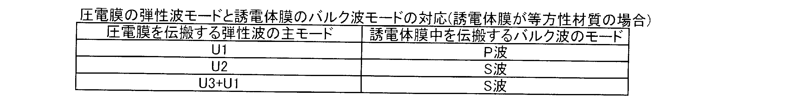
- the high acoustic velocity film 3 and the low acoustic velocity film 4 are isotropic with respect to the propagation direction of the bulk wave, the following Table 1 is obtained. That is, the high sound velocity and the low sound velocity are determined according to the right-axis bulk wave mode of Table 1 below with respect to the left-axis elastic wave main mode of Table 1 below.
- the P wave is a longitudinal wave
- the S wave is a transverse wave.
- U1 means a P wave as a main component
- U2 means an SH wave as a main component
- U3 means an elastic wave whose main component is an SV wave.
- the bulk wave mode for determining the high acoustic velocity and the low acoustic velocity is determined as shown in Table 2 below.
- the slower one of the SH wave and the SV wave is called a slow transverse wave
- the faster one is called a fast transverse wave.
- the slower transverse wave depends on the anisotropy of the material.
- the SV wave has a slow transverse wave
- the SH wave has a fast transverse wave among bulk waves.
- the low sound velocity film 4 is made of silicon oxide, and its film thickness is 0.35 ⁇ , where ⁇ is the wavelength of the elastic wave determined by the electrode period of the IDT electrode.
- an appropriate material having a bulk wave sound velocity lower than the bulk wave propagating through the piezoelectric film 5 can be used.
- a medium mainly composed of the above materials such as silicon oxide, glass, silicon oxynitride, tantalum oxide, or a compound obtained by adding fluorine, carbon, or boron to silicon oxide can be used.
- the low sound velocity film and the high sound velocity film are made of an appropriate dielectric material capable of realizing the high sound velocity and the low sound velocity determined as described above.
- the piezoelectric film 5 in the present embodiment in LiTaO 3 namely Euler angles 38.5 ° Y-cut (0 °, 128.5 °, 0 °) consists LiTaO 3, the thickness of the electrode of the IDT 6 When the wavelength of the surface acoustic wave determined by the period is ⁇ , it is 0.25 ⁇ .
- the piezoelectric film 5 may be formed of LiTaO 3 having another cut angle, or may be formed of a piezoelectric single crystal other than LiTaO 3 .
- the IDT electrode 6 is made of Al in this embodiment.
- the IDT electrode 6 can be formed of an appropriate metal material such as Al, Cu, Pt, Au, Ag, Ti, Ni, Cr, Mo, W, or an alloy mainly composed of any of these metals.
- the IDT electrode 6 may have a structure in which a plurality of metal films made of these metals or alloys are stacked.
- the electrode structure shown in FIG. 1B is formed on the piezoelectric film 5. That is, the IDT electrode 6 and the reflectors 7 and 8 disposed on both sides of the IDT electrode 6 in the surface acoustic wave electrode direction are formed. Thus, a 1-port surface acoustic wave resonator is configured.
- the electrode structure including the IDT electrode in the present invention is not particularly limited, and can be modified to constitute a ladder filter, a longitudinally coupled filter, a lattice type filter, and a transversal type filter that combine appropriate resonators and resonators. .
- the surface acoustic wave device 1 is characterized in that the high sound velocity film 3, the low sound velocity film 4, and the piezoelectric film 5 are laminated. Thereby, the Q value can be increased.
- the reason for this is as follows.
- the low acoustic velocity film 4 is disposed between the high acoustic velocity film 3 and the piezoelectric film 5, the acoustic velocity of the elastic wave is lowered.
- the energy of an elastic wave is concentrated in a medium that is essentially a low sound velocity. Therefore, the effect of confining the elastic wave energy in the piezoelectric film 5 and the IDT in which the elastic wave is excited can be enhanced. Therefore, compared with the case where the low sound velocity film 4 is not provided, according to this embodiment, loss can be reduced and Q value can be raised.
- the high acoustic velocity film 3 functions so as to confine the elastic wave in a portion where the piezoelectric film 5 and the low acoustic velocity film 4 are laminated so as not to leak into a structure below the high acoustic velocity film 3. That is, in the structure of the present application, the energy of the elastic wave of a specific mode used for obtaining the characteristics of the filter and the resonator is distributed throughout the piezoelectric film 5 and the low sonic film 4, and the low sonic film of the high sonic film 3 is used. It is distributed also to a part of the side and not distributed to the support substrate 2.
- the mechanism for confining the elastic wave by the high-velocity film is the same as that of the Love wave type surface wave which is a non-leakage SH wave.
- the mechanism is different from the confinement mechanism using a Bragg reflector with an acoustic multilayer film.
- the low acoustic velocity film 4 is made of silicon oxide, the temperature characteristics can be improved.
- the elastic constant of LiTaO 3 has a negative temperature characteristic, and silicon oxide has a positive temperature characteristic. Therefore, in the surface acoustic wave device 1, the absolute value of TCF can be reduced.
- the intrinsic acoustic impedance of silicon oxide is smaller than the intrinsic acoustic impedance of LiTaO 3 . Therefore, both the increase of the electromechanical coupling coefficient, that is, the expansion of the specific band and the improvement of the frequency temperature characteristic can be achieved.
- the electromechanical coupling coefficient can be adjusted within a wide range as will be described later. Therefore, the degree of freedom in design can be increased.
- the surface acoustic wave device 1 of the first embodiment and the surface acoustic wave devices of the following first and second comparative examples were created.
- First comparative example an electrode made of Al (thickness 0.08 ⁇ ) /38.5° Y-cut LiTaO 3 substrate in order from the top.
- the electrode made of Al was formed on a LiTaO 3 substrate having a thickness of 350 ⁇ m.
- Second comparative example Al electrode (thickness 0.08 ⁇ ) /38.5° Y-cut LiTaO 3 film thickness 0.5 ⁇ / aluminum nitride film (thickness 1.5 ⁇ ) / glass supporting substrate in order from the top.
- the electrodes are those of the 1-port surface acoustic wave resonator structure shown in FIG.
- the wavelength ⁇ of the surface acoustic wave determined by the electrode period of the IDT electrode was 2 ⁇ m.
- the main mode of the surface acoustic wave propagating through the 38.5 ° Y-cut LiTaO 3 is the U2 mode, and the sound velocity is about 3950 m / sec.
- the sound velocity of the bulk wave propagating through the rotated Y-cut LiTaO 3 is constant regardless of the rotation angle if it is on the Y-cut, the SV bulk wave (slow transverse wave) is 3367 m / sec, and the SH bulk wave (fast transverse wave). ) Is 4212 m / sec.
- the aluminum nitride film in the first embodiment and the second comparative example is an isotropic film, and the acoustic velocity of the bulk wave (S wave) in the aluminum nitride film is 6000 m / sec.
- the silicon oxide film as the low acoustic velocity film 4 created in the first embodiment is an isotropic film, and the acoustic velocity of the bulk wave (S wave) in silicon oxide is 3750 m / sec. Therefore, since the main mode of the surface wave propagating through the piezoelectric body is the U2 mode, the following condition is satisfied. (1) Bulk wave (S wave) sound velocity of high sound velocity film: 6000 m / sec> Sound velocity of main mode of surface wave (U2): 3950 m / sec, and (2) Bulk wave (S wave) sound velocity of low sound velocity film: 3750 m / sec ⁇ Bulk wave (SH) sound velocity propagating through piezoelectric film: 4212 m / sec
- FIG. 2 shows impedance frequency characteristics of the surface acoustic wave devices of the first embodiment and the first and second comparative examples
- FIG. 3 shows an impedance Smith chart.
- Table 3 below shows the Q value at the resonance frequency, the Q value at the anti-resonance frequency, the specific bandwidth, and the resonance frequency of the surface acoustic wave devices of the first embodiment and the first and second comparative examples. TCF was determined by actual measurement.
- the solid line shows the result of the first embodiment
- the broken line shows the result of the second comparative example
- the alternate long and short dash line shows the result of the first comparative example.
- the ratio of the valleys and valleys is larger than that of the first comparative example.
- the Yamatani ratio indicates the ratio of the impedance at the antiresonance frequency to the impedance at the resonance frequency, and a higher value can constitute a filter having a higher Q value and a smaller insertion loss.
- the ratio of the valley and the valley is further increased as compared with the second comparative example.
- the frequency difference between the resonance frequency and the anti-resonance frequency, that is, the ratio band can be increased according to the first embodiment as compared with the second comparative example.
- the Q value at the resonance frequency can be increased as compared with the first comparative example and the second comparative example. It can be seen that the Q value at the frequency can be significantly increased. That is, since a 1-port surface acoustic wave resonator having a high Q value can be formed, it can be seen that a filter with a small insertion loss can be formed using the surface acoustic wave device 1. Further, the specific band was 3.2% in the first comparative example and 4.1% in the second comparative example. On the other hand, in the said 1st Embodiment, it turns out that it becomes 4.4%.
- the alternate long and short dash line indicates the first embodiment
- the broken line indicates the result of the first comparative example
- the solid line indicates the result of the FEM simulation of the second comparative example.
- the low sound velocity film 4 made of silicon oxide is replaced with the high sound velocity film 3 made of aluminum nitride.
- the piezoelectric film 5 made of LiTaO 3 can be confirmed to increase the Q value.
- the Q value can be increased by efficiently confining the surface acoustic wave energy in the piezoelectric film 5, the low acoustic velocity film 4, and the high acoustic velocity film 3 by forming the high acoustic velocity film 3. This is considered to be because the effect of suppressing the leakage of the surface acoustic wave energy to the outside of the IDT electrode can be enhanced by the formation.
- the material constituting the piezoelectric film is the above 38.5 ° Y cut. It is not limited to LiTaO 3 . Similar effects can be obtained even when LiTaO 3 with other cut angles is used. Further, it is possible to obtain the same effect even in the case of using another piezoelectric single crystal, ZnO, such as LiNbO 3 other than LiTaO 3, a piezoelectric thin film such as AlN, the piezoelectric ceramic such as PZT.
- the high acoustic velocity film 3 serves to confine most of the surface acoustic wave energy in the portion where the piezoelectric film 5 and the low acoustic velocity film 4 are laminated. Therefore, the aluminum nitride film may be a C-axis oriented anisotropic film, and is not limited to the aluminum nitride film, and the same effect can be obtained even when the materials that can form the various high sound velocity films 3 described above are used. Can be expected.
- the silicon oxide of the low acoustic velocity film is not particularly limited as long as the acoustic velocity of the bulk wave is lower than the acoustic velocity of the bulk wave propagating through the piezoelectric film. Therefore, the material constituting the low acoustic velocity film 4 is not limited to silicon oxide. Therefore, the various materials illustrated as a material which can comprise the low-sonic-velocity film
- the IDT electrode was an Al film having a thickness of 0.08 ⁇ .
- the piezoelectric film was made of 38.5 ° Y-cut LiTaO 3 and had a thickness in the range of 0 to 3 ⁇ .
- the low acoustic velocity film is made of silicon oxide and has a thickness of 0 to 2 ⁇ .
- the high sound velocity film is made of aluminum oxide and has a thickness of 1.5 ⁇ .
- the support substrate is made of alumina.
- FIG. 7 is a diagram showing the relationship among the film thickness of LiTaO 3 , the sound speed of the U2 mode that is the mode to be used, and the normalized film thickness of the silicon oxide film.
- FIG. 7 is a diagram showing the relationship between the film thickness of LiTaO 3 , the electromechanical coupling coefficient k 2 of the U2 mode that is the mode to be used, and the normalized film thickness of the silicon oxide film.
- the normalized film thickness of the silicon oxide film is 0.0, that is, it is made of LiTaO 3 by forming the silicon oxide film as compared with the case where the silicon oxide film is not formed. It can be seen that there is little variation in sound speed over a wide range of the thickness of the piezoelectric film from 0.05 ⁇ to 0.5 ⁇ .
- the silicon oxide film is formed, so that even if the LiTaO 3 film is as thin as 0.35 ⁇ or less, the silicon oxide film is not formed.
- the electromechanical coupling coefficient k 2 can be seen to increase with 0.08 or more.
- FIG. 9 is a diagram showing the relationship between the film thickness of the LiTaO 3 film, the frequency temperature coefficient TCV, and the normalized film thickness of the silicon oxide film.
- FIG. 10 is a diagram illustrating the relationship between the film thickness of the LiTaO 3 film, the specific band, and the normalized film thickness of the silicon oxide film.
- TCF TCV- ⁇ . ⁇ indicates a linear expansion coefficient in the propagation direction, and is about 16 ppm / ° C. in the case of LiTaO 3 .
- the absolute value of TCV can be further reduced by forming the silicon oxide film as compared with the case where the silicon oxide film is not formed.
- the specific band is adjusted by adjusting the film thickness of the silicon oxide film. I know you get.
- the thickness of the silicon oxide film is greater than 2 ⁇ , stress is generated and the surface acoustic wave device is warped, which causes problems such as difficulty in handling. Therefore, the thickness of the silicon oxide film is preferably 2 ⁇ or less.
- FIG. 11 is a diagram showing the relationship between the ratio band and TCF in the following surface acoustic wave devices of third to fifth comparative examples as conventional surface acoustic wave devices.
- Third comparative example electrode made of Al / stacked structure of 42 ° Y-cut LiTaO 3 , using SH waves.
- Fourth comparative example Silicon oxide film / Cu electrode / stacked structure of 38.5 ° Y-cut LiTaO 3 substrate, using SH waves.
- FIG. 12 shows the ratio band when the normalized film thickness of LiTaO 3 of the surface acoustic wave device is changed in the range of 0.1 to 0.5 ⁇ at each silicon oxide film thickness level of the second embodiment. It is a figure which shows the relationship between BW (%) and frequency temperature coefficient TCV.
- BW %
- TCV frequency temperature coefficient
- the specific bandwidth is wide and the temperature characteristics are good. It can be seen that an acoustic wave device can be provided.
- the linear expansion coefficient of the support substrate 2 is preferably smaller than the linear expansion coefficient of the piezoelectric film 5. Thereby, expansion due to heat generated in the piezoelectric film 5 is restrained by the support substrate 2. Therefore, the frequency temperature characteristic of the acoustic wave device can be further improved.
- FIG. 13 and FIG. 14 are diagrams showing changes in sound velocity and specific band when the thickness of the piezoelectric film made of LiTaO 3 is changed in the structure of the second embodiment.
- the thickness of LiTaO 3 is 1.5 ⁇ or more, the sound speed and the specific band are not substantially changed. This is because the energy of the surface acoustic wave is confined in the piezoelectric film and is not distributed on the low sound velocity film 4 or the high sound velocity film 3 side. The effect of the film 3 is lost. Therefore, the thickness of the piezoelectric film is more preferably 1.5 ⁇ or less. Accordingly, it is considered that the energy of the surface acoustic wave can be sufficiently distributed in the low acoustic velocity film 4 and the Q value can be further increased.
- the electromechanical coupling coefficient can be adjusted within a wide range by adjusting the thickness of the silicon oxide film and the thickness of the piezoelectric film made of LiTaO 3 . Furthermore, it can be seen that when the thickness of the piezoelectric film made of LiTaO 3 is in the range of 0.05 ⁇ to 0.5 ⁇ , the electromechanical coupling coefficient can be adjusted in a wider range. Therefore, the thickness of the piezoelectric film made of LiTaO 3 is preferably in the range of 0.05 ⁇ to 0.5 ⁇ .
- the thickness of the silicon oxide film, that is, the low-sonic film is The electromechanical coupling coefficient can be freely adjusted by adjusting the thickness of the piezoelectric film. Therefore, the degree of freedom in design can be greatly increased. Accordingly, it is possible to easily satisfy various characteristics such as sound velocity, electromechanical coupling coefficient, frequency temperature characteristics, and spurious characteristics at the same time, and a surface acoustic wave device having desired characteristics can be easily provided.
- the IDT electrode 6 has a laminated structure of 0.08 ⁇ -thick Al film / piezoelectric film 4 as a 0.25 ⁇ -thick LiTaO 3 film / low-speed film 4 as a silicon oxide film / high-speed film in a thickness range of 0 to 2 ⁇ .
- As the high sound velocity film a silicon nitride film, an aluminum oxide film, and diamond were used.
- the film thickness of the high acoustic velocity film 3 was 1.5 ⁇ .
- 15 and 16 are diagrams showing the thickness of the silicon oxide film in the third embodiment, the sound velocity and the relationship between the electromechanical coupling coefficient k 2, respectively.
- the speed of sound of the bulk wave (S wave) of the silicon nitride film is 6000 m / sec
- the speed of sound of the bulk wave (S wave) in aluminum oxide is 6000 m / sec
- the sound velocity of the bulk wave (S wave) in diamond is 12800 m / sec.
- the electromechanical coupling coefficient is such that when the thickness of the silicon oxide film is 0.1 ⁇ or more, the thickness of the silicon oxide film is in the range of 0.1 ⁇ to 0.5 ⁇ regardless of the material of the high sound velocity film. It can be seen that there is almost no change within. Further, FIG. 15 shows that the sound speed does not change regardless of the material of the high sound speed film when the film thickness of the silicon oxide film is 0.3 ⁇ or more and 2 ⁇ or less.
- the material of the high sound velocity film is not particularly limited as long as the above conditions are satisfied.
- the laminated structure was IDT electrode 6 / piezoelectric film 5 / low sound velocity film 4 / high sound velocity film 3 / support substrate 2.
- IDT electrode 6 Al having a thickness of 0.08 ⁇ was used.
- LiTaO 3 having a thickness of 0.25 ⁇ was used as the piezoelectric film.
- silicon oxide having a thickness of 0.35 ⁇ was used.
- high acoustic velocity film 3 an aluminum nitride film having a thickness of 1.5 ⁇ was used. Glass was used as the support substrate 2.
- Electromechanical coupling coefficients were determined by FEM for a number of surface acoustic wave devices having the above-described structure in which ⁇ and ⁇ of Euler angles (0 °, ⁇ , ⁇ ) of the piezoelectric film were changed.
- the range of the electromechanical coupling coefficient k 2 modes mainly composed of U2 component (SH component) is 2% or more, was confirmed to be within the scope of a plurality of regions R1 shown in FIG. 17. The same result was obtained within the range of Euler angles (0 ° ⁇ 5, ⁇ , ⁇ ).
- the electromechanical coupling coefficient of the surface acoustic wave mainly including the U3 component (SV component) was obtained by FEM.
- the results are shown in FIG. In the range of a plurality of regions R2 shown in FIG. 18, the electromechanical coupling coefficient of the mode mainly composed of U2 (SH component) is 2% or more and the mode mainly composed of U3 component (SV component) is used.
- the electromechanical coupling coefficient is 1% or less.
- the electromechanical coupling coefficient of the U2 mode to be used is large and the electromechanical coupling coefficient of the U3 mode, which is spurious, can be reduced. Therefore, a bandpass filter having much better filter characteristics can be configured.
- a surface acoustic wave device having the following configuration was simulated as the sixth embodiment.
- Table 4 the characteristics of the surface wave mainly composed of the U2 component when the transverse acoustic velocity of the low acoustic velocity film and the natural acoustic impedance of the transverse velocity of the low acoustic velocity membrane are varied over 10 levels are finite. Simulated by the element method. It should be noted that the transverse sound velocity and the intrinsic acoustic impedance of the low sound velocity film changed the density and elastic constant of the low sound velocity film. Further, the material constants of the low acoustic velocity film not listed in Table 4 were all silicon oxide material constants.
- 1.11E + 03 means 1.11 ⁇ 10 3 . That is, aE + b indicates a ⁇ 10 b .
- the electrode structure was the same as that shown in FIG. 1B, and the surface acoustic wave device was a laminated structure of IDT electrode / piezoelectric film / low sound speed film / high sound speed film / support substrate.
- the IDT electrode was an Al film having a thickness of 0.08 ⁇ .
- the piezoelectric film is made of 40 ° Y-cut LiTaO 3 . When the thickness of this piezoelectric film was 0.1 ⁇ , 0.4 ⁇ , and 0.6 ⁇ , 10 levels shown in Table 4 were calculated.
- the thickness of the low acoustic velocity film was set to 0.4 ⁇ .
- the high sound velocity film is made of aluminum oxide and has a thickness of 1.5 ⁇ .
- the support substrate is made of an alumina substrate.
- FIGS. 19A to 19C are diagrams showing the relationship between the specific acoustic impedance of the low sound velocity film and the specific band in the sixth embodiment.
- Each level in the figure shows the behavior when the transverse sound velocity of the low-speed film changes, and the specific band of each level is normalized by the specific band when the specific acoustic impedance of the piezoelectric film is the same as the specific acoustic impedance of the low-speed film.
- the intrinsic acoustic impedance is represented by the product of the acoustic velocity of the bulk wave and the density of the medium.
- the bulk wave of the piezoelectric film is an SH bulk wave
- the acoustic velocity is 4212 m / s
- the density is 7 Since it is .454 ⁇ 10 3 kg / m 3
- the intrinsic acoustic impedance of the piezoelectric film is 3.14 ⁇ 10 7 N ⁇ s / m 3 .
- the acoustic velocity of the bulk wave used when calculating the intrinsic acoustic impedance of the low acoustic velocity film and the piezoelectric membrane is as shown in Tables 1 and 2 with respect to the main mode of the surface acoustic wave on the left axis in Tables 1 and 2. Is determined by the bulk wave mode of the right axis.
- FIGS. 20A to 20C are diagrams showing the relationship between the natural acoustic impedance of the transverse wave of the low acoustic velocity film and the acoustic velocity of the propagating surface acoustic wave in the sixth embodiment.
- the specific band increases as the specific acoustic impedance of the low-speed film is smaller than the specific acoustic impedance of the piezoelectric film, regardless of the thickness of the piezoelectric film.
- the inherent acoustic impedance of the low-velocity film is smaller than the intrinsic acoustic impedance of the piezoelectric film, so that the displacement of the piezoelectric film with respect to a certain stress becomes larger and generates a larger charge. It is because it is obtained.
- the specific acoustic impedance of the low sound velocity film is the specific impedance of the piezoelectric film regardless of the vibration mode of the surface acoustic wave, the type of the piezoelectric film, or the type of the low speed film. If it is smaller, a surface acoustic wave device with a larger specific band can be obtained.
- the IDT electrode 6, the piezoelectric film 5, the low acoustic velocity film 4, the high acoustic velocity film 3, and the support substrate 2 are laminated in this order from the top.
- an adhesive layer such as Ti or NiCr, a base film, or an arbitrary medium may exist between the respective layers within a range in which the surface acoustic wave and boundary wave that propagates are not greatly affected.
- a new high sound velocity film that is sufficiently thinner than the wavelength of the surface wave may be formed between the piezoelectric film 5 and the low sound velocity film 4, and the same effect can be obtained.
- the surface acoustic wave energy mainly used is not distributed between the high acoustic velocity film 3 and the support substrate 2. Therefore, any medium may be formed with any thickness between the high acoustic velocity film 3 and the support substrate 2, and the same effect can be obtained.
- the following seventh and eighth embodiments are embodiments of the surface acoustic wave device further including such a medium layer.
- the medium layer 22 is laminated between the support substrate 2 and the high acoustic velocity film 3.
- Other configurations are the same as those of the first embodiment. Therefore, the description of the first embodiment is incorporated. Therefore, in the surface acoustic wave device 21, the IDT electrode 6, the piezoelectric film 5, the low acoustic velocity film 4, the high acoustic velocity film 3, the medium layer 22, and the support substrate 2 are laminated in this order from the top.
- the medium layer 22 any material such as a dielectric, a piezoelectric, a semiconductor, or a metal may be used. Even in this case, the same effect as that of the first embodiment can be obtained. However, when the medium layer 22 is made of metal, the specific band can be reduced. Therefore, for applications where the specific bandwidth is small, the medium layer 22 is preferably made of metal.
- the medium layer 22 and the medium layer 24 are laminated between the support substrate 2 and the high acoustic velocity film 3. That is, the IDT electrode 6, the piezoelectric film 5, the low acoustic velocity film 4, the high acoustic velocity film 3, the medium layer 22, the medium layer 24, and the support substrate 2 are laminated in this order from the top. Except for the medium layer 22 and the medium layer 24, the configuration is the same as in the first embodiment.
- the medium layers 22 and 24 may use any material such as dielectric, piezoelectric, semiconductor, or metal. Even in this case, the same effects as those of the surface acoustic wave device of the first embodiment can be obtained in the eighth embodiment.
- the laminated structure composed of the piezoelectric film 5, the low acoustic velocity film 4, the high acoustic velocity film 3 and the medium layer 22 and the laminated structure composed of the medium layer 24 and the support substrate 2 are separately manufactured, and then both laminated structures are formed. Join. Thereafter, the IDT electrode 6 is formed on the piezoelectric film 5. Accordingly, the surface acoustic wave device according to the present embodiment can be obtained without depending on the manufacturing constraints when manufacturing each laminated structure. Therefore, the freedom degree of selection of the material which comprises each layer can be raised.
- any joining method can be used for joining the two laminated structures.
- various methods such as hydrophilic bonding, activation bonding, atomic diffusion bonding, metal diffusion bonding, anodic bonding, bonding with resin or SOG can be used.
- the bonding interface between the two laminated structures is located on the opposite side of the piezoelectric film 5 from the high sound velocity film 3. Therefore, the bonding interface exists in a portion below the high acoustic velocity film 3 where the energy of the main surface acoustic wave used is not distributed. Therefore, the surface acoustic wave propagation characteristics are not affected by the quality of the joint interface. Therefore, stable and good resonance characteristics and filter characteristics can be obtained.
- an IDT electrode 6, a piezoelectric film 5, a low acoustic velocity film 4, and a high acoustic velocity support substrate 33 that also functions as a high acoustic velocity film are laminated in this order from the top. That is, the high sound speed support substrate 33 serves as both the high sound speed film 3 and the support substrate 2 in the first embodiment. Therefore, the bulk sound velocity of the high sound velocity support substrate 33 is set to be higher than the sound velocity of the surface acoustic wave propagating through the piezoelectric film 5. Therefore, the same effect as the first embodiment can be obtained. In addition, since the high sonic support substrate 33 serves as both the high sonic film and the support substrate, the number of components can be reduced.
- the following structure is assumed as the surface acoustic wave device shown in the first embodiment, that is, the schematic front sectional view of FIG.
- a support substrate made of a film / a SiO 2 film having a thickness of 0.3 ⁇ / alumina was laminated in this order.
- the thickness of the LiTaO 3 film as the piezoelectric film was changed to 0.15 ⁇ , 0.20 ⁇ , 0.25 ⁇ , or 0.30 ⁇ .
- the film thickness of the SiO 2 film as the low acoustic velocity film was changed in the range of 0 to 2 ⁇ .
- the duty of the IDT electrode was 0.5, the electrode finger crossing width was 20 ⁇ , and the number of electrode fingers was 100 pairs.
- a 1-port surface acoustic wave resonator was prepared in which an IDT electrode made of Al with a thickness of 0.1 ⁇ / a 38.5 ° Y-cut LiTaO 3 substrate was laminated in this order from the top. That is, in this comparative example, an electrode structure having an IDT electrode made of Al is formed on a 38.5 ° Y-cut LiTaO 3 substrate having a thickness of 350 ⁇ m.
- the relationship between the Q value and the frequency was obtained by FEM simulation.
- the largest Q value within the frequency range of the resonance frequency at which the impedance of the one-port resonator is minimized and the anti-resonance frequency at which the impedance is maximized was defined as the Q max value.
- a larger Q max value indicates a lower loss.
- FIG. 26 shows the relationship among the LiTaO 3 film thickness, the SiO 2 film thickness, and Q max in the above embodiment.
- the acoustic wave device includes the high sound velocity film 3, the low sound velocity film 4, the piezoelectric film 5, and the IDT electrode 6 on the support substrate 2.
- the method for manufacturing such an acoustic wave device is not particularly limited.
- the elastic wave device 1 having a thin piezoelectric film can be easily obtained by using a manufacturing method using an ion implantation method described below. An embodiment of this manufacturing method will be described with reference to FIGS.
- a piezoelectric substrate 5A is prepared.
- the piezoelectric substrate 5A is made of LiTaO 3 .
- Hydrogen ions are implanted from one side of the piezoelectric substrate 5A.
- the ions to be implanted are not limited to hydrogen but helium or the like may be used.
- the energy at the time of ion implantation is not particularly limited.
- the energy is 107 KeV
- the dose is 8 ⁇ 10 16 atoms / cm 2 .
- an ion concentration distribution is generated in the thickness direction in the piezoelectric substrate 5A.
- a portion having the highest ion concentration is indicated by a broken line in FIG.
- the implanted ion high concentration portion 5a which is the portion having the highest ion concentration indicated by a broken line, when heated as described later, it is easily separated by stress.
- a method of separating by such an implanted ion high concentration portion 5a is disclosed in JP-T-2002-534886.
- the piezoelectric substrate 5A is separated at the implanted ion high concentration portion 5a to obtain the piezoelectric film 5.
- the piezoelectric film 5 is a layer between the surface of the piezoelectric substrate where ion implantation is started from the implanted ion high concentration portion 5a.
- the piezoelectric film 5 may be processed such as polishing. Therefore, the distance from the implanted ion high concentration portion 5a to the piezoelectric substrate surface on the ion implantation side may be the same as or slightly larger than the thickness of the finally formed piezoelectric film.
- the low acoustic velocity film 4 is formed on the surface of the piezoelectric substrate 5A on which ion implantation has been performed. Note that a low-velocity film formed in advance may be bonded to the piezoelectric substrate 5A by a transfer method or the like.
- the high sonic film 3 is formed on the surface of the low sonic film 4 opposite to the piezoelectric substrate 5A.
- the high sonic film 3 may be bonded to the low sonic film 4 by a transfer method or the like regardless of the film forming method.
- the exposed surface of the high sonic film 3, that is, the surface opposite to the low sonic film 4 is mirror-finished.
- Mirror surface processing can reinforce the bonding strength between a support substrate and a high-speed film described later.
- the support substrate 2 is bonded to the high sound velocity film 3.
- a silicon oxide film is used according to the first embodiment.
- an aluminum nitride film is used as the high sound velocity film 3.
- the piezoelectric substrate portion 5b above the implanted ion high concentration portion 5a is separated from the piezoelectric substrate 5A.
- the heating temperature in this case may be about 250 ° C. to 400 ° C.
- the piezoelectric film 5 having a thickness of 500 nm is obtained by this heat separation.
- a structure is obtained in which the piezoelectric film 5 is laminated on the low acoustic velocity film 4 as shown in FIG.
- a heat treatment is performed at a temperature of 400 ° C. to 500 ° C. for about 3 hours. If necessary, the upper surface of the separated piezoelectric film 5 may be polished prior to this heat treatment.
- an electrode including the IDT electrode 6 is formed.
- the electrode forming method is not particularly limited, and can be performed by an appropriate method such as vapor deposition, plating, or sputtering.
- the piezoelectric film 5 having an inclined Euler angle can be easily and uniformly formed by the above separation.
- the IDT electrode 6 / piezoelectric film 5 / low sound velocity film 4 / high sound velocity film 3 / support substrate 2 are laminated in this order from the top.
- the dielectric film 42 may be laminated so as to cover the IDT electrode 6.
- FIG. 28 is a schematic front sectional view showing a boundary acoustic wave device 43 as a twelfth embodiment.
- a boundary acoustic wave device 43 As a twelfth embodiment.
- a low sound velocity film 4 / a high sound velocity film 3 / a support substrate 2 are laminated in order from the top.
- This structure is the same as that of the first embodiment.
- the IDT electrode 6 is formed on the interface between the piezoelectric film 5 and the dielectric 44 laminated on the piezoelectric film 5.
- FIG. 29 is a schematic front sectional view of a so-called three-medium structure boundary acoustic wave device 45.
- the IDT electrode 6 is formed at the interface between the piezoelectric film 5 and the dielectric film 46 in contrast to the structure in which the low sound velocity film 4 / high sound velocity film 3 / support substrate 2 are laminated below the piezoelectric film 5.
- a dielectric 47 having a faster transverse wave speed than the dielectric 46 is laminated on the dielectric 46.
- a so-called three-medium structure boundary acoustic wave device is configured.
- the low acoustic velocity film 4 / the high acoustic velocity membrane 3 are disposed below the piezoelectric film 5 similarly to the surface acoustic wave device 1 of the first embodiment.
Landscapes
- Physics & Mathematics (AREA)
- Acoustics & Sound (AREA)
- Engineering & Computer Science (AREA)
- Manufacturing & Machinery (AREA)
- Surface Acoustic Wave Elements And Circuit Networks Thereof (AREA)
Abstract
Description


第2の実施形態として、以下の構成の弾性表面波装置について、その特性を有限要素法でシミュレーションした。電極構造は図1(b)と同様とした。 (Second Embodiment)
As a second embodiment, the characteristics of a surface acoustic wave device having the following configuration were simulated by a finite element method. The electrode structure was the same as in FIG.
第3の実施形態として、第1の実施形態と同様の弾性表面波装置を作製した。ただし、材料及び膜厚は以下の通りとした。 (Third embodiment)
As a third embodiment, a surface acoustic wave device similar to that of the first embodiment was produced. However, the material and film thickness were as follows.
第4の実施形態では、圧電膜のオイラー角(0°,θ,ψ)を変化させ、U2成分(SH成分)を主体とした弾性表面波の電気機械結合係数を求めた。 (Fourth embodiment)
In the fourth embodiment, the Euler angles (0 °, θ, ψ) of the piezoelectric film are changed, and the electromechanical coupling coefficient of the surface acoustic wave mainly including the U2 component (SH component) is obtained.
第4の実施形態と同じ構造を前提として、FEMにより、U3成分(SV成分)を主体とする弾性表面波の電気機械結合係数を求めた。そして、U2(SH成分)を主体とするモードの電気機械結合係数が2%以上であり、かつU3(SV成分)を主体とするモードの電気機械結合係数が1%以下となるオイラー角の範囲を求めた。結果を図18に示す。図18に示す複数の領域R2の範囲内であれば、U2(SH成分)を主体としたモードの電気機械結合係数が2%以上であり、かつU3成分(SV成分)を主体とするモードの電気機械結合係数が1%以下である。従って、複数の領域R2の範囲内にあるオイラー角のLiTaO3を用いることにより、利用するU2モードの電気機械結合係数が大きくかつスプリアスとなるU3モードの電気機械結合係数を小さくすることができる。従って、より一層良好なフィルタ特性を有する帯域フィルタを、構成することができる。 (Fifth embodiment)
On the premise of the same structure as that of the fourth embodiment, the electromechanical coupling coefficient of the surface acoustic wave mainly including the U3 component (SV component) was obtained by FEM. The range of Euler angles in which the electromechanical coupling coefficient of the mode mainly composed of U2 (SH component) is 2% or more and the electromechanical coupling coefficient of the mode mainly composed of U3 (SV component) is 1% or less. Asked. The results are shown in FIG. In the range of a plurality of regions R2 shown in FIG. 18, the electromechanical coupling coefficient of the mode mainly composed of U2 (SH component) is 2% or more and the mode mainly composed of U3 component (SV component) is used. The electromechanical coupling coefficient is 1% or less. Therefore, by using Euler angle LiTaO 3 within the range of the plurality of regions R2, the electromechanical coupling coefficient of the U2 mode to be used is large and the electromechanical coupling coefficient of the U3 mode, which is spurious, can be reduced. Therefore, a bandpass filter having much better filter characteristics can be configured.
第2の実施形態と同様に、第6の実施形態として、以下の構成の弾性表面波装置についてシミュレーションした。下記の表4に示すように、低音速膜の横波音速と低音速膜の横波の固有音響インピーダンスを10の水準に亘って変化させた場合のU2成分を主体とする表面波の特性を、有限要素法でシミュレーションした。なお、低音速膜の横波音速と固有音響インピーダンスは低音速膜の密度及び弾性定数を変化させた。また、表4に記されていない低音速膜の材料定数は全て酸化ケイ素の材料定数を使用した。 (Sixth embodiment)
Similar to the second embodiment, a surface acoustic wave device having the following configuration was simulated as the sixth embodiment. As shown in Table 4 below, the characteristics of the surface wave mainly composed of the U2 component when the transverse acoustic velocity of the low acoustic velocity film and the natural acoustic impedance of the transverse velocity of the low acoustic velocity membrane are varied over 10 levels are finite. Simulated by the element method. It should be noted that the transverse sound velocity and the intrinsic acoustic impedance of the low sound velocity film changed the density and elastic constant of the low sound velocity film. Further, the material constants of the low acoustic velocity film not listed in Table 4 were all silicon oxide material constants.

図23に示す第7の実施形態に係る弾性表面波装置21では、媒質層22が、支持基板2と高音速膜3との間に積層されている。その他の構成は、第1の実施形態と同様である。従って、第1の実施形態の説明を援用することとする。従って、弾性表面波装置21では、上から順に、IDT電極6、圧電膜5、低音速膜4、高音速膜3、媒質層22及び支持基板2がこの順序で積層されている。 (Seventh embodiment)
In the surface
図24に示す第8の実施形態の弾性表面波装置23では、支持基板2と高音速膜3との間に、媒質層22及び媒質層24が積層されている。すなわち、上から順に、IDT電極6、圧電膜5、低音速膜4、高音速膜3、媒質層22、媒質層24及び支持基板2がこの順序で積層されている。媒質層22及び媒質層24以外は、第1の実施形態と同様に構成されている。 (Eighth embodiment)
In the surface
図25に示す弾性表面波装置31では、上から順に、IDT電極6、圧電膜5、低音速膜4、高音速膜としても機能する高音速支持基板33がこの順序で積層されている。すなわち、高音速支持基板33は、第1の実施形態における高音速膜3と支持基板2の双方を兼ねている。従って、高音速支持基板33のバルク波音速は、圧電膜5を伝搬する弾性表面波の音速よりも高速とされている。よって、第1の実施形態と同様の効果を得ることができる。しかも、高音速支持基板33が高音速膜及び支持基板を兼ねているため、部品点数の低減を図ることができる。 (Ninth embodiment)
In the surface
第10の実施形態として、弾性表面波装置として1ポート型弾性表面波共振子におけるQ値と周波数との関係をFEMによりシミュレーションした。 (Tenth embodiment)
As a tenth embodiment, the relationship between the Q value and frequency in a 1-port surface acoustic wave resonator as a surface acoustic wave device was simulated by FEM.
第1の実施形態に係る弾性波装置は、前述したように、支持基板2上に、高音速膜3、低音速膜4、圧電膜5及びIDT電極6を備える。このような弾性波装置の製造方法は特に限定されない。もっとも、次に述べるイオン注入法を利用した製造方法を用いることにより、厚みの薄い圧電膜を有する弾性波装置1を容易に得ることができる。この製造方法の実施形態を、図21及び図22を参照して説明する。 (Embodiment of manufacturing method)
As described above, the acoustic wave device according to the first embodiment includes the high
第1の実施形態では、IDT電極6/圧電膜5/低音速膜4/高音速膜3/支持基板2が上から順にこの順序で積層されていた。本発明においては、図27に示す第11の実施形態の弾性表面波装置41のように、IDT電極6を覆うように誘電体膜42が積層されていてもよい。このような誘電体膜42を積層することにより、周波数温度特性を調整したり、耐湿性を高めたりすることができる。 (Eleventh embodiment)
In the first embodiment, the
上述してきた各実施形態では弾性表面波装置につき説明したが、本発明は、弾性境界波装置などの他の弾性波装置にも適用することができ、その場合であっても同様の効果を得ることができる。図28は、第12の実施形態としての弾性境界波装置43を示す模式的正面断面図である。ここでは、圧電膜5の下方に、上から順に低音速膜4/高音速膜3/支持基板2が積層されている。この構造は、第1の実施形態と同様である。そして、弾性境界波を励振するために、圧電膜5と圧電膜5上に積層された誘電体44との界面にIDT電極6が形成されている。 (Twelfth embodiment)
In each of the embodiments described above, the surface acoustic wave device has been described, but the present invention can also be applied to other surface acoustic wave devices such as a boundary acoustic wave device, and even in that case, the same effect can be obtained. be able to. FIG. 28 is a schematic front sectional view showing a boundary
2…支持基板
3…高音速膜
4…低音速膜
5…圧電膜
5A…圧電基板
5a…注入イオン高濃度部分
6…IDT電極
7,8…反射器 DESCRIPTION OF
Claims (19)
- 圧電膜を有する弾性波装置であって、
前記圧電膜を伝搬する弾性波音速より伝搬するバルク波音速が高速である高音速支持基板と、
前記高音速支持基板上に積層されており、前記圧電膜を伝搬するバルク波音速より伝搬するバルク波音速が低速である低音速膜と、
前記低音速膜上に積層された前記圧電膜と、
前記圧電膜の一方面に形成されているIDT電極とを備える、弾性波装置。 An acoustic wave device having a piezoelectric film,
A high sound velocity support substrate having a bulk wave sound velocity propagating higher than an elastic wave sound velocity propagating through the piezoelectric film;
A low-velocity film laminated on the high-velocity support substrate and having a low bulk-wave sound velocity propagating from the bulk-wave sound velocity propagating through the piezoelectric film;
The piezoelectric film laminated on the low sound velocity film;
An elastic wave device comprising: an IDT electrode formed on one surface of the piezoelectric film. - 前記圧電膜を伝搬する弾性波のエネルギーの一部が、前記低音速膜および前記高音速支持基板中に分布することを特徴とする、請求項1に記載の弾性波装置。 2. The elastic wave device according to claim 1, wherein a part of energy of the elastic wave propagating through the piezoelectric film is distributed in the low sound velocity film and the high sound velocity support substrate.
- 圧電膜を有する弾性波装置であって、
支持基板と、
前記支持基板上に形成されており、前記圧電膜を伝搬する弾性波音速より伝搬するバルク波音速が高速である高音速膜と、
前記高音速膜上に積層されており、前記圧電膜を伝搬するバルク波音速より伝搬するバルク波音速が低速である低音速膜と、
前記低音速膜上に積層された前記圧電膜と、
前記圧電膜の一方面に形成されているIDT電極とを備える、弾性波装置。 An acoustic wave device having a piezoelectric film,
A support substrate;
A high sound velocity film formed on the support substrate and having a higher bulk wave sound velocity propagating from the acoustic wave velocity propagating through the piezoelectric film;
A low-velocity film that is laminated on the high-velocity film and has a lower bulk-wave sound speed than the bulk-wave sound speed that propagates through the piezoelectric film;
The piezoelectric film laminated on the low sound velocity film;
An elastic wave device comprising: an IDT electrode formed on one surface of the piezoelectric film. - 前記圧電膜を伝搬する弾性波のエネルギーの一部が、前記低音速膜および前記高音速膜中に分布することを特徴とする、請求項3に記載の弾性波装置。 4. The acoustic wave device according to claim 3, wherein a part of energy of the elastic wave propagating through the piezoelectric film is distributed in the low acoustic velocity film and the high acoustic velocity film.
- 前記低音速膜が、酸化ケイ素、あるいは酸化ケイ素を主成分とする膜からなる、請求項1~4のいずれか1項に記載の弾性波装置。 5. The acoustic wave device according to claim 1, wherein the low acoustic velocity film is made of silicon oxide or a film mainly composed of silicon oxide.
- 前記圧電膜の膜厚が、IDT電極の電極周期で定まる弾性波の波長をλとしたときに、1.5λ以下とされている、請求項1~5のいずれか1項に記載の弾性波装置。 The elastic wave according to any one of claims 1 to 5, wherein the film thickness of the piezoelectric film is 1.5λ or less, where λ is a wavelength of an elastic wave determined by an electrode period of the IDT electrode. apparatus.
- 前記圧電膜の膜厚が、IDT電極の電極周期で定まる弾性波の波長をλとしたときに、0.05λ~0.5λの範囲とされている、請求項1~6のいずれか1項に記載の弾性波装置。 The film thickness of the piezoelectric film is in a range of 0.05λ to 0.5λ, where λ is a wavelength of an elastic wave determined by an electrode period of the IDT electrode. The elastic wave device described in 1.
- 前記低音速膜の膜厚が、IDT電極の電極周期で定まる弾性波の波長をλとしたときに、2λ以下である、請求項1~7のいずれか1項に記載の弾性波装置。 The elastic wave device according to any one of claims 1 to 7, wherein a film thickness of the low acoustic velocity film is 2λ or less when a wavelength of an elastic wave determined by an electrode period of the IDT electrode is λ.
- 前記圧電膜が、オイラー角(0±5°,θ,ψ)の単結晶タンタル酸リチウムからなり、オイラー角(0±5°,θ,ψ)が図17に示す複数の領域R1のいずれかの範囲内にある、請求項1~8のいずれか1項に記載の弾性波装置。 The piezoelectric film is made of single crystal lithium tantalate having an Euler angle (0 ± 5 °, θ, ψ), and the Euler angle (0 ± 5 °, θ, ψ) is one of the plurality of regions R1 shown in FIG. The elastic wave device according to any one of claims 1 to 8, which falls within the range of:
- 前記圧電膜が、オイラー角(0±5°,θ,ψ)が、図18の複数の領域R2のいずれかの範囲内にある、請求項9に記載の弾性波装置。 The elastic wave device according to claim 9, wherein the piezoelectric film has an Euler angle (0 ± 5 °, θ, ψ) in any one of the plurality of regions R2 in Fig. 18.
- 前記支持基板の線膨張係数が、前記圧電膜の線膨張係数よりも小さい、請求項1~10のいずれか1項に記載の弾性波装置。 The elastic wave device according to any one of claims 1 to 10, wherein a linear expansion coefficient of the support substrate is smaller than a linear expansion coefficient of the piezoelectric film.
- 前記低音速膜の固有音響インピーダンスが、前記圧電膜の固有音響インピーダンスよりも小さい、請求項1~11のいずれか1項に記載の弾性波装置。 The elastic wave device according to any one of claims 1 to 11, wherein a specific acoustic impedance of the low sound velocity film is smaller than a specific acoustic impedance of the piezoelectric film.
- 前記圧電膜および前記IDT電極の上に誘電体膜が形成されており、前記圧電膜を弾性表面波が伝搬する、請求項1~12のいずれか1項に記載の弾性波装置。 The elastic wave device according to any one of claims 1 to 12, wherein a dielectric film is formed on the piezoelectric film and the IDT electrode, and a surface acoustic wave propagates through the piezoelectric film.
- 前記圧電膜および前記IDT電極の上に誘電体膜が形成されており、前記圧電膜と前記誘電体膜との境界を弾性境界波が伝搬する、請求項1~12のいずれか1項に記載の弾性波装置。 The dielectric film is formed on the piezoelectric film and the IDT electrode, and an elastic boundary wave propagates through a boundary between the piezoelectric film and the dielectric film. Elastic wave device.
- 前記圧電膜および前記低音速膜および前記高音速膜および前記支持基板の少なくとも1つの境界に、密着層、下地膜、低音速層及び高音速層の内の少なくとも1つの層が形成されている、請求項1~14のいずれか1項に記載の弾性波装置。 At least one of an adhesion layer, a base film, a low sound velocity layer, and a high sound velocity layer is formed on at least one boundary of the piezoelectric film, the low sound velocity film, the high sound velocity film, and the support substrate. The elastic wave device according to any one of claims 1 to 14.
- 支持基板を用意する工程と、
前記支持基板上に、圧電体を伝搬する弾性波音速より伝搬するバルク波音速が高速である高音速膜を形成する工程と、
前記高音速膜上に、圧電体を伝搬するバルク波音速より伝搬するバルク波音速が低速である低音速膜を形成する工程と、
前記低音速膜上に、圧電体層を形成する工程と、
前記圧電体層の一方面にIDT電極を形成する工程とを備える、弾性波装置の製造方法。 Preparing a support substrate;
On the support substrate, forming a high acoustic velocity film having a high bulk acoustic wave velocity propagating from the acoustic wave acoustic velocity propagating through the piezoelectric body;
A step of forming a low sound velocity film on which the bulk wave sound velocity propagating from the bulk wave sound velocity propagating through the piezoelectric body is low on the high sound velocity film;
Forming a piezoelectric layer on the low acoustic velocity film;
And a step of forming an IDT electrode on one surface of the piezoelectric layer. - 前記支持基板上に、前記高音速膜、前記低音速膜及び前記圧電体層を形成する工程が、
(a)前記圧電体層よりも厚みの厚い圧電基板の一方面からイオン注入する工程と、
(b)前記イオン注入が行われた圧電基板の前記一方の面に低音速膜を形成する工程と、
(c)前記低音速膜の前記圧電基板と反対側の面に高音速膜を形成する工程と、
(d)前記高音速膜の前記低音速膜が積層されている側の面と反対側の面に支持基板を接合する工程と、
(e)前記圧電基板を加熱しつつ、前記圧電基板の注入イオン濃度が最も高い高濃度イオン注入部分において、圧電膜と残りの圧電基板部分とを分離し、前記低音速膜側に圧電膜を残存させる工程とを備える、請求項16に記載の弾性波装置の製造方法。 Forming the high sound velocity film, the low sound velocity film and the piezoelectric layer on the support substrate;
(A) a step of ion-implanting from one surface of a piezoelectric substrate thicker than the piezoelectric layer;
(B) forming a low speed film on the one surface of the piezoelectric substrate on which the ion implantation has been performed;
(C) forming a high sound velocity film on a surface of the low sound velocity film opposite to the piezoelectric substrate;
(D) bonding a support substrate to a surface opposite to the surface on which the low sound velocity film of the high sound velocity film is laminated;
(E) While heating the piezoelectric substrate, the piezoelectric film is separated from the remaining piezoelectric substrate portion in the high concentration ion implanted portion where the implanted ion concentration of the piezoelectric substrate is the highest, and the piezoelectric film is disposed on the low sound velocity film side. The manufacturing method of the elastic wave apparatus of Claim 16 provided with the process made to remain. - 前記残りの圧電基板部分を分離した後に、前記低音速膜上に積層されている前記圧電膜を加熱し、圧電性を回復させる工程をさらに備える、請求項17に記載の弾性波装置の製造方法。 The method for manufacturing an acoustic wave device according to claim 17, further comprising a step of heating the piezoelectric film laminated on the low sound velocity film to recover the piezoelectricity after separating the remaining piezoelectric substrate portion. .
- 前記支持基板を接合するに先立ち、前記高音速膜の前記低音速膜と反対側の面を鏡面加工する工程とを備える、請求項16または17に記載の弾性波装置の製造方法。 The method for manufacturing an acoustic wave device according to claim 16 or 17, further comprising a step of mirror-finishing the surface of the high-sonic film opposite to the low-sonic film prior to bonding the support substrate.
Priority Applications (12)
| Application Number | Priority Date | Filing Date | Title |
|---|---|---|---|
| JP2012549827A JP5713025B2 (en) | 2010-12-24 | 2011-12-20 | Elastic wave device and manufacturing method thereof |
| CN201180059880.4A CN103262410B (en) | 2010-12-24 | 2011-12-20 | Acoustic wave device and manufacture method thereof |
| KR1020137015786A KR101534654B1 (en) | 2010-12-24 | 2011-12-20 | Elastic wave device and production method thereof |
| EP11850979.3A EP2658123B1 (en) | 2010-12-24 | 2011-12-20 | Elastic wave device and method for manufacturing the same. |
| KR1020157012867A KR101623099B1 (en) | 2010-12-24 | 2011-12-20 | Elastic wave device and production method thereof |
| US13/920,492 US9431996B2 (en) | 2010-12-24 | 2013-06-18 | Elastic wave device and method for manufacturing the same |
| US14/488,447 US9484885B2 (en) | 2010-12-24 | 2014-09-17 | Method of manufacturing elastic wave device |
| US15/212,489 US9831848B2 (en) | 2010-12-24 | 2016-07-18 | Elastic wave device and method for manufacturing the same |
| US15/666,596 US10511279B2 (en) | 2010-12-24 | 2017-08-02 | Elastic wave device and method for manufacturing the same |
| US16/680,891 US11509280B2 (en) | 2010-12-24 | 2019-11-12 | Elastic wave device and method for manufacturing the same |
| US17/968,828 US11863152B2 (en) | 2010-12-24 | 2022-10-19 | Elastic wave device and method for manufacturing the same |
| US18/515,882 US20240088863A1 (en) | 2010-12-24 | 2023-11-21 | Elastic wave device and method for manufacturing the same |
Applications Claiming Priority (2)
| Application Number | Priority Date | Filing Date | Title |
|---|---|---|---|
| JP2010-288453 | 2010-12-24 | ||
| JP2010288453 | 2010-12-24 |
Related Child Applications (1)
| Application Number | Title | Priority Date | Filing Date |
|---|---|---|---|
| US13/920,492 Continuation US9431996B2 (en) | 2010-12-24 | 2013-06-18 | Elastic wave device and method for manufacturing the same |
Publications (1)
| Publication Number | Publication Date |
|---|---|
| WO2012086639A1 true WO2012086639A1 (en) | 2012-06-28 |
Family
ID=46313908
Family Applications (1)
| Application Number | Title | Priority Date | Filing Date |
|---|---|---|---|
| PCT/JP2011/079496 WO2012086639A1 (en) | 2010-12-24 | 2011-12-20 | Elastic wave device and production method thereof |
Country Status (6)
| Country | Link |
|---|---|
| US (7) | US9431996B2 (en) |
| EP (1) | EP2658123B1 (en) |
| JP (2) | JP5713025B2 (en) |
| KR (2) | KR101623099B1 (en) |
| CN (2) | CN106209007B (en) |
| WO (1) | WO2012086639A1 (en) |
Cited By (94)
| Publication number | Priority date | Publication date | Assignee | Title |
|---|---|---|---|---|
| US20140203893A1 (en) * | 2011-09-30 | 2014-07-24 | Murata Manufacturing Co., Ltd. | Elastic wave device |
| CN104205629A (en) * | 2012-03-23 | 2014-12-10 | 株式会社村田制作所 | Elastic wave device and manufacturing method for same |
| US20150102705A1 (en) * | 2012-06-22 | 2015-04-16 | Murata Manufacturing Co., Ltd. | Elastic wave device |
| WO2015080045A1 (en) * | 2013-11-29 | 2015-06-04 | 株式会社村田製作所 | Splitter |
| JP2015109622A (en) * | 2013-12-06 | 2015-06-11 | 株式会社村田製作所 | Longitudinal coupling resonator type surface acoustic wave filter |
| JP2015109574A (en) * | 2013-12-05 | 2015-06-11 | 株式会社村田製作所 | Longitudinal coupling resonator type surface acoustic wave filter and communication instrument |
| JP2015115870A (en) * | 2013-12-13 | 2015-06-22 | 株式会社村田製作所 | Acoustic wave device |
| JP2015119450A (en) * | 2013-12-20 | 2015-06-25 | 株式会社村田製作所 | Surface acoustic wave device and communication apparatus |
| JP2015119244A (en) * | 2013-12-17 | 2015-06-25 | 株式会社村田製作所 | Acoustic wave filter device |
| JP2015119452A (en) * | 2013-12-20 | 2015-06-25 | 株式会社村田製作所 | Surface acoustic wave filter |
| JP2015119451A (en) * | 2013-12-20 | 2015-06-25 | 株式会社村田製作所 | Surface acoustic wave filter |
| JP2015119310A (en) * | 2013-12-18 | 2015-06-25 | 株式会社村田製作所 | Surface acoustic wave filter |
| JP2015119258A (en) * | 2013-12-17 | 2015-06-25 | 株式会社村田製作所 | Acoustic wave filter device |
| JP2015119449A (en) * | 2013-12-20 | 2015-06-25 | 株式会社村田製作所 | Surface acoustic wave filter |
| JP2015119370A (en) * | 2013-12-19 | 2015-06-25 | 株式会社村田製作所 | Surface acoustic wave filter |
| WO2015098756A1 (en) * | 2013-12-26 | 2015-07-02 | 株式会社村田製作所 | Elastic wave device and filter apparatus |
| WO2015098678A1 (en) * | 2013-12-27 | 2015-07-02 | 株式会社村田製作所 | Elastic wave device |
| JP2015122566A (en) * | 2013-12-20 | 2015-07-02 | 株式会社村田製作所 | Acoustic wave device |
| WO2015137089A1 (en) * | 2014-03-14 | 2015-09-17 | 株式会社村田製作所 | Acoustic wave device |
| WO2015151705A1 (en) * | 2014-03-31 | 2015-10-08 | 株式会社村田製作所 | Surface acoustic wave filter |
| WO2015186661A1 (en) * | 2014-06-04 | 2015-12-10 | 株式会社村田製作所 | Elastic wave device |
| WO2015198904A1 (en) * | 2014-06-26 | 2015-12-30 | 株式会社村田製作所 | Longitudinally coupled resonator type surface acoustic wave filter |
| WO2016047255A1 (en) * | 2014-09-26 | 2016-03-31 | 国立大学法人東北大学 | Elastic wave device |
| JP2016072808A (en) * | 2014-09-30 | 2016-05-09 | 株式会社村田製作所 | Duplexer and method of manufacturing the same |
| WO2016084526A1 (en) * | 2014-11-28 | 2016-06-02 | 株式会社村田製作所 | Elastic wave device |
| WO2016103953A1 (en) * | 2014-12-25 | 2016-06-30 | 株式会社村田製作所 | Acoustic wave device |
| WO2016147986A1 (en) * | 2015-03-16 | 2016-09-22 | 株式会社村田製作所 | Elastic wave device and production method for same |
| WO2016208446A1 (en) * | 2015-06-24 | 2016-12-29 | 株式会社村田製作所 | Filter device |
| WO2016208236A1 (en) * | 2015-06-22 | 2016-12-29 | 株式会社村田製作所 | Elastic wave filter device |
| JPWO2015098679A1 (en) * | 2013-12-27 | 2017-03-23 | 株式会社村田製作所 | Elastic wave device and manufacturing method thereof |
| KR20170128505A (en) | 2015-07-17 | 2017-11-22 | 가부시키가이샤 무라타 세이사쿠쇼 | Seismic wave device |
| KR20170134626A (en) | 2015-06-25 | 2017-12-06 | 가부시키가이샤 무라타 세이사쿠쇼 | Seismic wave device |
| KR20170136600A (en) | 2015-06-25 | 2017-12-11 | 가부시키가이샤 무라타 세이사쿠쇼 | Seismic wave device |
| WO2018003837A1 (en) * | 2016-06-29 | 2018-01-04 | 株式会社村田製作所 | Multiplexer and method for manufacturing same |
| KR20180009354A (en) | 2015-06-25 | 2018-01-26 | 가부시키가이샤 무라타 세이사쿠쇼 | Multiplexer, high-frequency front-end circuit and communication device |
| KR20180021171A (en) | 2015-09-07 | 2018-02-28 | 가부시키가이샤 무라타 세이사쿠쇼 | Seismic wave device, high frequency front end circuit and communication device |
| US9935611B2 (en) | 2014-04-11 | 2018-04-03 | Murata Manufacturing Co., Ltd. | Elastic wave filter device |
| WO2018062321A1 (en) * | 2016-09-30 | 2018-04-05 | 株式会社村田製作所 | High-frequency front end circuit and communication device |
| KR20180041738A (en) | 2015-10-23 | 2018-04-24 | 가부시키가이샤 무라타 세이사쿠쇼 | Seismic wave device |
| JP2018074575A (en) * | 2016-10-20 | 2018-05-10 | スカイワークス ソリューションズ, インコーポレイテッドSkyworks Solutions, Inc. | Elastic wave device with sub-wavelength thick piezoelectric layer |
| WO2018092511A1 (en) * | 2016-11-18 | 2018-05-24 | 株式会社村田製作所 | Surface acoustic wave filter and multiplexer |
| WO2018096783A1 (en) * | 2016-11-22 | 2018-05-31 | 株式会社村田製作所 | Elastic wave device, front end circuit, and communication device |
| WO2018164211A1 (en) * | 2017-03-09 | 2018-09-13 | 株式会社村田製作所 | Multiplexer, high-frequency front end circuit, and communication device |
| WO2018168655A1 (en) * | 2017-03-15 | 2018-09-20 | 株式会社村田製作所 | Multiplexer, high frequency front end circuit, and communication device |
| JP2018534863A (en) * | 2015-10-20 | 2018-11-22 | ソイテック | Method for manufacturing a hybrid structure |
| US10148245B2 (en) | 2015-06-25 | 2018-12-04 | Murata Manufacturing Co., Ltd. | Elastic wave device |
| WO2019022236A1 (en) * | 2017-07-27 | 2019-01-31 | 京セラ株式会社 | Elastic wave device, duplexer, and communication device |
| JP2019507546A (en) * | 2016-01-28 | 2019-03-14 | コーボ ユーエス,インコーポレイティド | Surface acoustic wave device including piezoelectric layer on quartz substrate and method for manufacturing the same |
| WO2019049608A1 (en) * | 2017-09-07 | 2019-03-14 | 株式会社村田製作所 | Acoustic wave device, high frequency front end circuit and communication device |
| WO2019065619A1 (en) * | 2017-09-29 | 2019-04-04 | 株式会社村田製作所 | Elastic wave device |
| JP2019080313A (en) * | 2017-10-23 | 2019-05-23 | コーボ ユーエス,インコーポレイティド | Quartz orientation for guided saw devices |
| KR20190065249A (en) | 2016-10-06 | 2019-06-11 | 신에쓰 가가꾸 고교 가부시끼가이샤 | Composite Substrate and Manufacturing Method of Composite Substrate |
| JP2019097145A (en) * | 2017-11-22 | 2019-06-20 | 住友金属鉱山株式会社 | Composite substrate for surface acoustic wave element, and manufacturing method thereof |
| KR20190075116A (en) | 2016-12-27 | 2019-06-28 | 가부시키가이샤 무라타 세이사쿠쇼 | Multiplexer, high-frequency front-end circuit and communication device |
| CN110166017A (en) * | 2018-02-16 | 2019-08-23 | 株式会社村田制作所 | Acoustic wave device, multiplexer, high-frequency front-end circuit and communication device |
| CN110166016A (en) * | 2018-02-16 | 2019-08-23 | 株式会社村田制作所 | Acoustic wave device, high-frequency front-end circuit and communication device |
| KR20190099065A (en) | 2017-02-10 | 2019-08-23 | 가부시키가이샤 무라타 세이사쿠쇼 | Acoustic Wave Device, High Frequency Front End Circuit and Communication Device |
| WO2019163842A1 (en) * | 2018-02-26 | 2019-08-29 | 京セラ株式会社 | Elastic wave element |
| WO2019194140A1 (en) * | 2018-04-03 | 2019-10-10 | 株式会社村田製作所 | Elastic wave device |
| JP2019193260A (en) * | 2018-04-18 | 2019-10-31 | スカイワークス ソリューションズ, インコーポレイテッドSkyworks Solutions, Inc. | Acoustic wave device with multi-layer piezoelectric substrate |
| JP2019201345A (en) * | 2018-05-17 | 2019-11-21 | 太陽誘電株式会社 | Acoustic wave resonator, filter and multiplexer |
| KR20190135542A (en) | 2017-05-26 | 2019-12-06 | 가부시키가이샤 무라타 세이사쿠쇼 | Acoustic Wave Devices, Filters, High Frequency Front End Circuits and Communication Devices |
| JP2019220794A (en) * | 2018-06-18 | 2019-12-26 | 株式会社村田製作所 | Acoustic wave device and high frequency front end circuit |
| KR20200036026A (en) | 2017-09-29 | 2020-04-06 | 가부시키가이샤 무라타 세이사쿠쇼 | Multiplexer, high frequency front end circuit and communication device |
| WO2020080465A1 (en) * | 2018-10-19 | 2020-04-23 | 株式会社村田製作所 | Elastic wave device |
| US10659001B2 (en) | 2015-06-25 | 2020-05-19 | Murata Manufacturing Co., Ltd. | Elastic wave device |
| JP2020096221A (en) * | 2018-12-10 | 2020-06-18 | 株式会社村田製作所 | Acoustic wave device, high-frequency front-end circuit, and communication device |
| JP2020096220A (en) * | 2018-12-10 | 2020-06-18 | 株式会社村田製作所 | Acoustic wave device, high-frequency front-end circuit, and communication device |
| JP2020123855A (en) * | 2019-01-30 | 2020-08-13 | 太陽誘電株式会社 | Elastic wave resonator, filter, and multiplexer |
| JP2020145530A (en) * | 2019-03-05 | 2020-09-10 | 京セラ株式会社 | Elastic wave device |
| JP2020156003A (en) * | 2019-03-22 | 2020-09-24 | 株式会社村田製作所 | Acoustic wave device |
| JP2020182130A (en) * | 2019-04-25 | 2020-11-05 | 太陽誘電株式会社 | Filter and multiplexer |
| WO2020261808A1 (en) * | 2019-06-28 | 2020-12-30 | 株式会社村田製作所 | Elastic wave filter |
| JP2021005785A (en) * | 2019-06-26 | 2021-01-14 | 信越化学工業株式会社 | Composite substrate for surface acoustic wave device and manufacturing method thereof |
| KR20210030459A (en) | 2018-09-20 | 2021-03-17 | 가부시키가이샤 무라타 세이사쿠쇼 | Acoustic wave device |
| KR20210083311A (en) | 2018-12-20 | 2021-07-06 | 가부시키가이샤 무라타 세이사쿠쇼 | Acoustic wave elements and seismic devices |
| KR20210087537A (en) | 2018-12-13 | 2021-07-12 | 가부시키가이샤 무라타 세이사쿠쇼 | seismic device |
| US11115003B2 (en) | 2018-01-12 | 2021-09-07 | Murata Manufacturing Co., Ltd. | Acoustic wave device, multiplexer, high-frequency front end circuit, and communication apparatus |
| WO2021177341A1 (en) * | 2020-03-03 | 2021-09-10 | 株式会社村田製作所 | Acoustic wave device |
| WO2021177340A1 (en) * | 2020-03-03 | 2021-09-10 | 株式会社村田製作所 | Acoustic wave device |
| KR20210126087A (en) | 2019-04-08 | 2021-10-19 | 가부시키가이샤 무라타 세이사쿠쇼 | seismic device |
| WO2021225102A1 (en) | 2020-05-08 | 2021-11-11 | 信越化学工業株式会社 | Method for manufacturing composite substrate provided with piezoelectric single crystal film |
| WO2021241434A1 (en) * | 2020-05-28 | 2021-12-02 | 株式会社村田製作所 | Elastic wave device |
| WO2021241435A1 (en) * | 2020-05-28 | 2021-12-02 | 株式会社村田製作所 | Elastic wave device |
| US11218134B2 (en) | 2017-09-07 | 2022-01-04 | Murata Manufacturing Co., Ltd. | Acoustic wave filter device and composite filter device |
| US11271545B2 (en) | 2017-09-29 | 2022-03-08 | Murata Manufacturing Co., Ltd. | Multiplexer, radio-frequency front end circuit, and communication device |
| US11309861B2 (en) | 2016-01-28 | 2022-04-19 | Qorvo Us, Inc. | Guided surface acoustic wave device providing spurious mode rejection |
| KR20220075403A (en) | 2019-11-06 | 2022-06-08 | 가부시키가이샤 무라타 세이사쿠쇼 | seismic device |
| KR20220082034A (en) | 2019-12-19 | 2022-06-16 | 가부시키가이샤 무라타 세이사쿠쇼 | seismic device |
| WO2022173038A1 (en) * | 2021-02-15 | 2022-08-18 | 株式会社村田製作所 | Elastic wave device and ladder-type filter |
| US11451206B2 (en) | 2015-07-28 | 2022-09-20 | Qorvo Us, Inc. | Methods for fabrication of bonded wafers and surface acoustic wave devices using same |
| US11456719B2 (en) | 2019-06-06 | 2022-09-27 | Murata Manufacturing Co., Ltd. | Acoustic wave device |
| US11496226B2 (en) | 2018-01-12 | 2022-11-08 | Murata Manufacturing Co., Ltd. | Acoustic wave device, multiplexer, high-frequency front end circuit, and communication device |
| US11764880B2 (en) | 2018-01-12 | 2023-09-19 | Murata Manufacturing Co., Ltd. | Acoustic wave device, multiplexer, high-frequency front end circuit, and communication device |
Families Citing this family (95)
| Publication number | Priority date | Publication date | Assignee | Title |
|---|---|---|---|---|
| JP5713025B2 (en) * | 2010-12-24 | 2015-05-07 | 株式会社村田製作所 | Elastic wave device and manufacturing method thereof |
| WO2013031724A1 (en) * | 2011-09-01 | 2013-03-07 | 株式会社村田製作所 | Piezoelectric bulk wave device and production method therefor |
| CN105723608B (en) * | 2013-10-18 | 2019-04-19 | 上海交通大学 | Piezoelectric ceramics planar motor and its driving method |
| JP6385690B2 (en) * | 2014-03-05 | 2018-09-05 | 太陽誘電株式会社 | Elastic wave device and manufacturing method thereof |
| WO2015137090A1 (en) * | 2014-03-13 | 2015-09-17 | 株式会社村田製作所 | Elastic wave device |
| KR101923572B1 (en) * | 2015-03-16 | 2018-11-29 | 가부시키가이샤 무라타 세이사쿠쇼 | Seismic wave device and manufacturing method thereof |
| WO2016199475A1 (en) | 2015-06-11 | 2016-12-15 | 株式会社村田製作所 | Low-noise amplifier and electronic device |
| WO2016208670A1 (en) * | 2015-06-24 | 2016-12-29 | 株式会社村田製作所 | Multiplexer, transmission device, reception device, high-frequency front-end circuit, communication device, and impedance matching method for multiplexer |
| KR102058177B1 (en) | 2015-06-24 | 2019-12-20 | 가부시키가이샤 무라타 세이사쿠쇼 | Acoustic Wave Filters, Multiplexers, Duplexers, High-Frequency Front-End Circuits, and Communications |
| US10659002B2 (en) * | 2015-06-25 | 2020-05-19 | Murata Manufacturing Co., Ltd. | Elastic wave device |
| JP6494462B2 (en) * | 2015-07-29 | 2019-04-03 | 太陽誘電株式会社 | Acoustic wave devices and modules |
| KR102011467B1 (en) * | 2015-09-10 | 2019-08-16 | 가부시키가이샤 무라타 세이사쿠쇼 | Acoustic Wave Device, High Frequency Front End Circuit and Communication Device |
| TWI625516B (en) * | 2015-09-15 | 2018-06-01 | Ngk Insulators Ltd | Method for estimating thickness tendency of composite substrate and piezoelectric substrate |
| CN108028637B (en) * | 2015-10-23 | 2021-05-11 | 株式会社村田制作所 | Elastic wave device |
| FR3045933B1 (en) * | 2015-12-22 | 2018-02-09 | Soitec | SUBSTRATE FOR ACOUSTIC SURFACE WAVE OR ACOUSTIC WAVE DEVICE OF TEMPERATURE COMPENSATED VOLUME |
| CN105978520B (en) * | 2016-05-12 | 2019-04-05 | 电子科技大学 | A kind of SAW device of multilayered structure and preparation method thereof |
| FR3052298B1 (en) * | 2016-06-02 | 2018-07-13 | Soitec | HYBRID STRUCTURE FOR ACOUSTIC SURFACE WAVE DEVICE |
| US10715105B2 (en) | 2016-06-24 | 2020-07-14 | Murata Manufacturing Co., Ltd. | Acoustic wave device |
| JP6642499B2 (en) * | 2016-06-24 | 2020-02-05 | 株式会社村田製作所 | Elastic wave device |
| WO2018003296A1 (en) * | 2016-06-29 | 2018-01-04 | 株式会社村田製作所 | Multiplexer, high-frequency front end circuit, and communication device |
| KR102132777B1 (en) * | 2016-09-13 | 2020-07-10 | 가부시키가이샤 무라타 세이사쿠쇼 | Seismic device, high frequency front end circuit and communication device |
| US10848121B2 (en) | 2016-10-14 | 2020-11-24 | Qorvo Us, Inc. | Guided SAW device |
| US10924085B2 (en) | 2016-10-17 | 2021-02-16 | Qorvo Us, Inc. | Guided acoustic wave device |
| WO2018079485A1 (en) * | 2016-10-25 | 2018-05-03 | 株式会社村田製作所 | Elastic wave device |
| KR101953219B1 (en) * | 2016-11-24 | 2019-02-28 | 가부시키가이샤 무라타 세이사쿠쇼 | Elastic wave device, high-frequency front end circuit, and communication apparatus |
| US10658564B2 (en) * | 2016-11-24 | 2020-05-19 | Huawei Technologies Co., Ltd. | Surface acoustic wave device |
| JP6547916B2 (en) * | 2016-12-20 | 2019-07-24 | 株式会社村田製作所 | Elastic wave device, high frequency front end circuit and communication device |
| US10594292B2 (en) * | 2017-01-30 | 2020-03-17 | Huawei Technologies Co., Ltd. | Surface acoustic wave device |
| JP6770106B2 (en) * | 2017-02-14 | 2020-10-14 | 京セラ株式会社 | Elastic wave element |
| KR102215432B1 (en) * | 2017-03-09 | 2021-02-16 | 가부시키가이샤 무라타 세이사쿠쇼 | Acoustic wave devices, multiplexers, high-frequency front-end circuits and communication devices |
| WO2018163841A1 (en) * | 2017-03-09 | 2018-09-13 | 株式会社村田製作所 | Elastic wave device, electric wave device package, multiplexer, high-frequency front end circuit, and communications device |
| WO2018163842A1 (en) * | 2017-03-09 | 2018-09-13 | 株式会社村田製作所 | Elastic wave device, high-frequency front end circuit, and communications device |
| US11522515B2 (en) | 2017-03-16 | 2022-12-06 | Skyworks Solutions, Inc. | Acoustic wave device including interdigital electrodes covered by silicon oxynitride film |
| JP6777221B2 (en) * | 2017-03-23 | 2020-10-28 | 株式会社村田製作所 | Elastic wave device |
| TWI780103B (en) * | 2017-05-02 | 2022-10-11 | 日商日本碍子股份有限公司 | Elastic wave element and method of manufacturing the same |
| WO2018235433A1 (en) * | 2017-06-21 | 2018-12-27 | 株式会社村田製作所 | Acoustic wave device |
| KR102345526B1 (en) * | 2017-09-19 | 2021-12-30 | 가부시키가이샤 무라타 세이사쿠쇼 | Acoustic wave filter device and multiplexer |
| JP2019062424A (en) * | 2017-09-27 | 2019-04-18 | 株式会社村田製作所 | Elastic wave device, high frequency front end circuit and communication device |
| JP6725083B2 (en) * | 2017-09-27 | 2020-07-15 | 株式会社村田製作所 | Elastic wave device and method of manufacturing elastic wave device |
| JP2019091978A (en) * | 2017-11-13 | 2019-06-13 | 株式会社村田製作所 | Acoustic wave device, high frequency front end circuit and communication device |
| JP2019092095A (en) * | 2017-11-16 | 2019-06-13 | 株式会社村田製作所 | Acoustic wave device, high frequency front end circuit and communication device |
| JP6950658B2 (en) * | 2017-11-29 | 2021-10-13 | 株式会社村田製作所 | Elastic wave device |
| JP2019102883A (en) * | 2017-11-29 | 2019-06-24 | 株式会社村田製作所 | Elastic wave device, high frequency front end circuit and communication device |
| US11677378B2 (en) * | 2017-11-29 | 2023-06-13 | Murata Manufacturing Co., Ltd. | Elastic wave device |
| CN111434037B (en) * | 2017-12-08 | 2023-09-08 | 株式会社村田制作所 | Elastic wave device |
| JP2019114986A (en) * | 2017-12-25 | 2019-07-11 | 株式会社村田製作所 | Acoustic wave device |
| WO2019130905A1 (en) | 2017-12-25 | 2019-07-04 | 株式会社村田製作所 | High-frequency apparatus |
| CN108039872A (en) * | 2017-12-26 | 2018-05-15 | 海宁市瑞宏科技有限公司 | A kind of resonator structure for high-performance SAW filter designs |
| US10700662B2 (en) | 2017-12-28 | 2020-06-30 | Taiyo Yuden Co., Ltd. | Acoustic wave device, filter, and multiplexer |
| WO2019130852A1 (en) | 2017-12-28 | 2019-07-04 | 日本碍子株式会社 | Assembly of piezoelectric material substrate and support substrate, and method for manufacturing said assembly |
| JP6648338B2 (en) | 2017-12-28 | 2020-02-14 | 日本碍子株式会社 | Bonded body of piezoelectric material substrate and support substrate and method of manufacturing the same |
| KR102404966B1 (en) | 2017-12-28 | 2022-06-07 | 엔지케이 인슐레이터 엘티디 | A bonding body of a piezoelectric material substrate and a supporting substrate and an acoustic wave element |
| KR102282238B1 (en) | 2018-02-13 | 2021-07-27 | 엔지케이 인슐레이터 엘티디 | Bonding body of piezoelectric material substrate and support substrate |
| JP7080671B2 (en) * | 2018-02-27 | 2022-06-06 | NDK SAW devices株式会社 | Surface acoustic wave device |
| WO2019177028A1 (en) * | 2018-03-14 | 2019-09-19 | 株式会社村田製作所 | Elastic wave device |
| JP6812998B2 (en) * | 2018-03-19 | 2021-01-13 | 株式会社村田製作所 | Elastic wave device |
| FR3079666B1 (en) * | 2018-03-30 | 2020-04-03 | Soitec | HYBRID STRUCTURE FOR SURFACE ACOUSTIC WAVE DEVICE AND MANUFACTURING METHOD THEREOF |
| CN108631747A (en) * | 2018-04-12 | 2018-10-09 | 无锡市好达电子有限公司 | A kind of SAW filter materials |
| US11595019B2 (en) | 2018-04-20 | 2023-02-28 | Taiyo Yuden Co., Ltd. | Acoustic wave resonator, filter, and multiplexer |
| DE102018109833A1 (en) * | 2018-04-24 | 2019-10-24 | RF360 Europe GmbH | SAW resonator, RF filter, multiplexer and method of making a SAW resonator |
| JP6599595B1 (en) * | 2018-05-16 | 2019-10-30 | 日本碍子株式会社 | Bonded body of piezoelectric material substrate and support substrate |
| CN112074622B (en) * | 2018-05-16 | 2021-07-27 | 日本碍子株式会社 | Bonded body of piezoelectric material substrate and support substrate |
| KR102312794B1 (en) | 2018-05-16 | 2021-10-15 | 엔지케이 인슐레이터 엘티디 | Bonding body of piezoelectric material substrate and support substrate |
| US11264966B2 (en) * | 2018-06-15 | 2022-03-01 | Resonant Inc. | Solidly-mounted transversely-excited film bulk acoustic resonator with diamond layers in Bragg reflector stack |
| US20220060170A1 (en) * | 2018-06-15 | 2022-02-24 | Resonant Inc. | Solidly-mounted transversely-excited film bulk acoustic device |
| JP6835041B2 (en) * | 2018-06-21 | 2021-02-24 | 株式会社村田製作所 | Multiplexer |
| CN112385144A (en) | 2018-07-03 | 2021-02-19 | 株式会社村田制作所 | Elastic wave device |
| DE102018217892A1 (en) | 2018-10-18 | 2020-04-23 | Fraunhofer-Gesellschaft zur Förderung der angewandten Forschung e.V. | Electroacoustic resonator and method for its production |
| WO2020122005A1 (en) * | 2018-12-10 | 2020-06-18 | 株式会社村田製作所 | Elastic wave device |
| DE102018132862A1 (en) * | 2018-12-19 | 2020-06-25 | RF360 Europe GmbH | Acoustic surface wave resonator and multiplexer that includes it |
| CN113228509B (en) | 2018-12-25 | 2024-04-16 | 株式会社村田制作所 | Filter device |
| JP2020145567A (en) * | 2019-03-06 | 2020-09-10 | 株式会社村田製作所 | Acoustic wave device |
| DE102019109031A1 (en) * | 2019-04-05 | 2020-10-08 | RF360 Europe GmbH | SAW device |
| WO2020209359A1 (en) * | 2019-04-12 | 2020-10-15 | 株式会社村田製作所 | Elastic wave device |
| US11664780B2 (en) | 2019-05-14 | 2023-05-30 | Skyworks Solutions, Inc. | Rayleigh mode surface acoustic wave resonator |
| JP7292100B2 (en) | 2019-05-16 | 2023-06-16 | NDK SAW devices株式会社 | Surface acoustic wave devices, filter circuits and electronic components |
| DE102019119239A1 (en) * | 2019-07-16 | 2021-01-21 | RF360 Europe GmbH | multiplexer |
| DE102019121804A1 (en) * | 2019-08-13 | 2021-02-18 | RF360 Europe GmbH | Ultra high frequency microacoustic device |
| US11356075B2 (en) * | 2019-09-16 | 2022-06-07 | Tohoku University | Surface acoustic wave device having mass-loaded electrode |
| CN110572135B (en) * | 2019-09-17 | 2021-12-14 | 中国科学院上海微系统与信息技术研究所 | High-frequency acoustic wave resonator and preparation method thereof |
| JP7433873B2 (en) | 2019-12-06 | 2024-02-20 | 太陽誘電株式会社 | Acoustic wave resonators, filters, and multiplexers |
| KR102319996B1 (en) | 2020-01-03 | 2021-11-01 | (주)와이솔 | Surface Acoustic Wave element and method manufacturing thereof |
| JP7485478B2 (en) * | 2020-03-13 | 2024-05-16 | 太陽誘電株式会社 | Acoustic Wave Devices, Filters and Multiplexers |
| JP7188412B2 (en) | 2020-04-17 | 2022-12-13 | 株式会社村田製作所 | Acoustic wave device and composite filter device |
| CN111786645B (en) * | 2020-05-07 | 2021-04-16 | 诺思(天津)微系统有限责任公司 | Bulk acoustic wave resonator, filter, electronic device, and method of adjusting electromechanical coupling coefficient |
| JP2021180465A (en) | 2020-05-15 | 2021-11-18 | 信越化学工業株式会社 | Composite substrate for surface acoustic wave device and method for manufacturing the same |
| WO2022050260A1 (en) | 2020-09-03 | 2022-03-10 | 株式会社村田製作所 | Elastic wave device |
| CN112398456A (en) * | 2020-11-20 | 2021-02-23 | 天通瑞宏科技有限公司 | High-performance surface acoustic wave device and preparation method thereof |
| CN112702037A (en) * | 2020-12-18 | 2021-04-23 | 广东广纳芯科技有限公司 | Lamb wave resonator with POI structure |
| CN116458062A (en) | 2020-12-22 | 2023-07-18 | 株式会社村田制作所 | Elastic wave device |
| CN112838838A (en) * | 2020-12-30 | 2021-05-25 | 广东广纳芯科技有限公司 | Surface acoustic wave resonator with single crystal PMNT and manufacturing method |
| CN112953445B (en) * | 2021-04-13 | 2023-09-15 | 广东广纳芯科技有限公司 | Resonator and method for manufacturing resonator |
| WO2022224470A1 (en) | 2021-04-20 | 2022-10-27 | 株式会社村田製作所 | Resonator |
| CN113872557B (en) * | 2021-09-29 | 2022-07-12 | 北京超材信息科技有限公司 | Composite substrate for surface acoustic wave device, manufacturing method thereof and surface acoustic wave device |
| CN117118388B (en) * | 2023-08-21 | 2024-04-16 | 天通瑞宏科技有限公司 | Multilayer composite wafer and thin film elastic wave device |
Citations (10)
| Publication number | Priority date | Publication date | Assignee | Title |
|---|---|---|---|---|
| JPH11274883A (en) * | 1998-03-20 | 1999-10-08 | Sumitomo Electric Ind Ltd | Piezoelectric compound substrate and surface acoustic wave element |
| JP2002534886A (en) | 1998-12-30 | 2002-10-15 | タレス | Device and method for surface acoustic waves guided in a thin layer of piezoelectric material bonded to a carrier substrate by a molecular binder |
| JP2003017967A (en) * | 2001-06-29 | 2003-01-17 | Toshiba Corp | Surface acoustic wave element and its manufacturing method |
| JP2004282232A (en) | 2003-03-13 | 2004-10-07 | Seiko Epson Corp | Surface acoustic wave device |
| JP2005354650A (en) * | 2004-02-05 | 2005-12-22 | Seiko Epson Corp | Surface acoustic wave device |
| JP2006270360A (en) * | 2005-03-23 | 2006-10-05 | Seiko Epson Corp | Surface acoustic wave element |
| JP2007228120A (en) * | 2006-02-22 | 2007-09-06 | Shin Etsu Chem Co Ltd | Surface acoustic wave element |
| JP2007228225A (en) * | 2006-02-23 | 2007-09-06 | Seiko Epson Corp | Surface acoustic wave device |
| JP2008067289A (en) * | 2006-09-11 | 2008-03-21 | Fujitsu Media Device Kk | Surface acoustic wave device and filter |
| JP2010251964A (en) * | 2009-04-14 | 2010-11-04 | Murata Mfg Co Ltd | Elastic wave filter and communication device |
Family Cites Families (26)
| Publication number | Priority date | Publication date | Assignee | Title |
|---|---|---|---|---|
| US4482833A (en) * | 1981-04-01 | 1984-11-13 | Westinghouse Electric Corp. | Method for obtaining oriented gold and piezoelectric films |
| JP3233489B2 (en) * | 1993-03-19 | 2001-11-26 | ティーディーケイ株式会社 | Surface acoustic wave device and method of manufacturing the same |
| JP2888158B2 (en) * | 1995-01-18 | 1999-05-10 | 日本電気株式会社 | Manufacturing method of surface acoustic wave device |
| US5759753A (en) * | 1995-07-19 | 1998-06-02 | Matsushita Electric Industrial Co., Ltd. | Piezoelectric device and method of manufacturing the same |
| US7105980B2 (en) * | 2002-07-03 | 2006-09-12 | Sawtek, Inc. | Saw filter device and method employing normal temperature bonding for producing desirable filter production and performance characteristics |
| JP4024741B2 (en) * | 2003-10-20 | 2007-12-19 | 富士通メディアデバイス株式会社 | Piezoelectric thin film resonator and filter |
| JP4419962B2 (en) * | 2004-01-19 | 2010-02-24 | 株式会社村田製作所 | Boundary acoustic wave device |
| JP4423976B2 (en) * | 2004-01-21 | 2010-03-03 | セイコーエプソン株式会社 | Thin film surface acoustic wave devices |
| JP4192794B2 (en) * | 2004-01-26 | 2008-12-10 | セイコーエプソン株式会社 | Piezoelectric element, piezoelectric actuator, ink jet recording head, ink jet printer, surface acoustic wave element, frequency filter, oscillator, electronic circuit, thin film piezoelectric resonator, and electronic device |
| CN101741342A (en) | 2004-03-29 | 2010-06-16 | 株式会社村田制作所 | Boundary acoustic wave device |
| JP2006025396A (en) * | 2004-06-09 | 2006-01-26 | Seiko Epson Corp | Surface acoustic wave device, method of manufacturing the same, and electronic equipment |
| JP2006013576A (en) * | 2004-06-22 | 2006-01-12 | Epson Toyocom Corp | Saw device and apparatus employing the same |
| FR2882205B1 (en) * | 2005-02-16 | 2007-06-22 | Centre Nat Rech Scient | HIGH-FREQUENCY ACOUSTIC WAVE DEVICE |
| JP4937605B2 (en) * | 2006-03-07 | 2012-05-23 | 太陽誘電株式会社 | Boundary acoustic wave device |
| US7463118B2 (en) * | 2006-06-09 | 2008-12-09 | Texas Instruments Incorporated | Piezoelectric resonator with an efficient all-dielectric Bragg reflector |
| WO2007145057A1 (en) * | 2006-06-16 | 2007-12-21 | Murata Manufacturing Co., Ltd. | Surface acoustic wave device |
| WO2008081695A1 (en) * | 2006-12-27 | 2008-07-10 | Murata Manufacturing Co., Ltd. | Surface acoustic wave device |
| JP2008136238A (en) * | 2008-02-08 | 2008-06-12 | Murata Mfg Co Ltd | Surface wave instrument and its manufacturing method |
| JP2010068503A (en) * | 2008-08-13 | 2010-03-25 | Seiko Epson Corp | Surface acoustic wave element |
| WO2010079575A1 (en) | 2009-01-07 | 2010-07-15 | 株式会社村田製作所 | Elastic boundary wave device |
| WO2011004665A1 (en) * | 2009-07-07 | 2011-01-13 | 株式会社村田製作所 | Elastic wave device and manufacturing method of elastic wave device |
| WO2011018913A1 (en) * | 2009-08-10 | 2011-02-17 | 株式会社村田製作所 | Boundary acoustic wave device |
| JP2011041127A (en) * | 2009-08-17 | 2011-02-24 | Hitachi Media Electoronics Co Ltd | Elastic wave device |
| JP5713025B2 (en) * | 2010-12-24 | 2015-05-07 | 株式会社村田製作所 | Elastic wave device and manufacturing method thereof |
| JP5648695B2 (en) * | 2010-12-24 | 2015-01-07 | 株式会社村田製作所 | Elastic wave device and manufacturing method thereof |
| JP2013214954A (en) * | 2012-03-07 | 2013-10-17 | Taiyo Yuden Co Ltd | Resonator, frequency filter, duplexer, electronic device, and method for manufacturing resonator |
-
2011
- 2011-12-20 JP JP2012549827A patent/JP5713025B2/en active Active
- 2011-12-20 KR KR1020157012867A patent/KR101623099B1/en active IP Right Grant
- 2011-12-20 KR KR1020137015786A patent/KR101534654B1/en active IP Right Grant
- 2011-12-20 CN CN201610512603.9A patent/CN106209007B/en active Active
- 2011-12-20 CN CN201180059880.4A patent/CN103262410B/en active Active
- 2011-12-20 EP EP11850979.3A patent/EP2658123B1/en active Active
- 2011-12-20 WO PCT/JP2011/079496 patent/WO2012086639A1/en active Application Filing
-
2013
- 2013-06-18 US US13/920,492 patent/US9431996B2/en active Active
-
2014
- 2014-09-17 US US14/488,447 patent/US9484885B2/en active Active
-
2015
- 2015-01-06 JP JP2015000617A patent/JP5910763B2/en active Active
-
2016
- 2016-07-18 US US15/212,489 patent/US9831848B2/en active Active
-
2017
- 2017-08-02 US US15/666,596 patent/US10511279B2/en active Active
-
2019
- 2019-11-12 US US16/680,891 patent/US11509280B2/en active Active
-
2022
- 2022-10-19 US US17/968,828 patent/US11863152B2/en active Active
-
2023
- 2023-11-21 US US18/515,882 patent/US20240088863A1/en active Pending
Patent Citations (10)
| Publication number | Priority date | Publication date | Assignee | Title |
|---|---|---|---|---|
| JPH11274883A (en) * | 1998-03-20 | 1999-10-08 | Sumitomo Electric Ind Ltd | Piezoelectric compound substrate and surface acoustic wave element |
| JP2002534886A (en) | 1998-12-30 | 2002-10-15 | タレス | Device and method for surface acoustic waves guided in a thin layer of piezoelectric material bonded to a carrier substrate by a molecular binder |
| JP2003017967A (en) * | 2001-06-29 | 2003-01-17 | Toshiba Corp | Surface acoustic wave element and its manufacturing method |
| JP2004282232A (en) | 2003-03-13 | 2004-10-07 | Seiko Epson Corp | Surface acoustic wave device |
| JP2005354650A (en) * | 2004-02-05 | 2005-12-22 | Seiko Epson Corp | Surface acoustic wave device |
| JP2006270360A (en) * | 2005-03-23 | 2006-10-05 | Seiko Epson Corp | Surface acoustic wave element |
| JP2007228120A (en) * | 2006-02-22 | 2007-09-06 | Shin Etsu Chem Co Ltd | Surface acoustic wave element |
| JP2007228225A (en) * | 2006-02-23 | 2007-09-06 | Seiko Epson Corp | Surface acoustic wave device |
| JP2008067289A (en) * | 2006-09-11 | 2008-03-21 | Fujitsu Media Device Kk | Surface acoustic wave device and filter |
| JP2010251964A (en) * | 2009-04-14 | 2010-11-04 | Murata Mfg Co Ltd | Elastic wave filter and communication device |
Non-Patent Citations (1)
| Title |
|---|
| See also references of EP2658123A4 |
Cited By (198)
| Publication number | Priority date | Publication date | Assignee | Title |
|---|---|---|---|---|
| US20140203893A1 (en) * | 2011-09-30 | 2014-07-24 | Murata Manufacturing Co., Ltd. | Elastic wave device |
| US9190981B2 (en) * | 2011-09-30 | 2015-11-17 | Murata Manufacturing Co., Ltd. | Elastic wave device including a supporting substrate, medium layer, and piezoelectric body |
| CN104205629A (en) * | 2012-03-23 | 2014-12-10 | 株式会社村田制作所 | Elastic wave device and manufacturing method for same |
| US20150102705A1 (en) * | 2012-06-22 | 2015-04-16 | Murata Manufacturing Co., Ltd. | Elastic wave device |
| WO2015080045A1 (en) * | 2013-11-29 | 2015-06-04 | 株式会社村田製作所 | Splitter |
| JPWO2015080045A1 (en) * | 2013-11-29 | 2017-03-16 | 株式会社村田製作所 | Duplexer |
| US9882548B2 (en) | 2013-11-29 | 2018-01-30 | Murata Manufacturing Co., Ltd. | Splitter |
| JP2015109574A (en) * | 2013-12-05 | 2015-06-11 | 株式会社村田製作所 | Longitudinal coupling resonator type surface acoustic wave filter and communication instrument |
| JP2015109622A (en) * | 2013-12-06 | 2015-06-11 | 株式会社村田製作所 | Longitudinal coupling resonator type surface acoustic wave filter |
| JP2015115870A (en) * | 2013-12-13 | 2015-06-22 | 株式会社村田製作所 | Acoustic wave device |
| JP2015119244A (en) * | 2013-12-17 | 2015-06-25 | 株式会社村田製作所 | Acoustic wave filter device |
| JP2015119258A (en) * | 2013-12-17 | 2015-06-25 | 株式会社村田製作所 | Acoustic wave filter device |
| JP2015119310A (en) * | 2013-12-18 | 2015-06-25 | 株式会社村田製作所 | Surface acoustic wave filter |
| JP2015119370A (en) * | 2013-12-19 | 2015-06-25 | 株式会社村田製作所 | Surface acoustic wave filter |
| JP2015119449A (en) * | 2013-12-20 | 2015-06-25 | 株式会社村田製作所 | Surface acoustic wave filter |
| JP2015119451A (en) * | 2013-12-20 | 2015-06-25 | 株式会社村田製作所 | Surface acoustic wave filter |
| JP2015119452A (en) * | 2013-12-20 | 2015-06-25 | 株式会社村田製作所 | Surface acoustic wave filter |
| JP2015122566A (en) * | 2013-12-20 | 2015-07-02 | 株式会社村田製作所 | Acoustic wave device |
| JP2015119450A (en) * | 2013-12-20 | 2015-06-25 | 株式会社村田製作所 | Surface acoustic wave device and communication apparatus |
| DE112014006013B4 (en) | 2013-12-26 | 2024-06-20 | Murata Manufacturing Co., Ltd. | Elastic wave device and filter device |
| JPWO2015098756A1 (en) * | 2013-12-26 | 2017-03-23 | 株式会社村田製作所 | Elastic wave device and filter device |
| US10447240B2 (en) | 2013-12-26 | 2019-10-15 | Murata Manufacturing Co., Ltd. | Elastic wave device and filter device |
| WO2015098756A1 (en) * | 2013-12-26 | 2015-07-02 | 株式会社村田製作所 | Elastic wave device and filter apparatus |
| DE112014006039B4 (en) | 2013-12-27 | 2022-08-25 | Murata Manufacturing Co., Ltd. | Elastic wave device and manufacturing method thereof |
| WO2015098678A1 (en) * | 2013-12-27 | 2015-07-02 | 株式会社村田製作所 | Elastic wave device |
| CN105794108B (en) * | 2013-12-27 | 2019-01-11 | 株式会社村田制作所 | Acoustic wave device |
| DE112014006080B4 (en) | 2013-12-27 | 2022-05-12 | Murata Manufacturing Co., Ltd. | Device for elastic waves |
| CN105794108A (en) * | 2013-12-27 | 2016-07-20 | 株式会社村田制作所 | Elastic wave device |
| US10243536B2 (en) | 2013-12-27 | 2019-03-26 | Murata Manufacturing Co., Ltd. | Elastic wave device and manufacturing method thereof |
| US10320362B2 (en) | 2013-12-27 | 2019-06-11 | Murata Manufacturing Co., Ltd. | Elastic wave device |
| JPWO2015098679A1 (en) * | 2013-12-27 | 2017-03-23 | 株式会社村田製作所 | Elastic wave device and manufacturing method thereof |
| JPWO2015098678A1 (en) * | 2013-12-27 | 2017-03-23 | 株式会社村田製作所 | Elastic wave device |
| WO2015137089A1 (en) * | 2014-03-14 | 2015-09-17 | 株式会社村田製作所 | Acoustic wave device |
| US10454448B2 (en) | 2014-03-14 | 2019-10-22 | Murata Manufacturing Co., Ltd. | Elastic wave device |
| JPWO2015137089A1 (en) * | 2014-03-14 | 2017-04-06 | 株式会社村田製作所 | Elastic wave device |
| WO2015151705A1 (en) * | 2014-03-31 | 2015-10-08 | 株式会社村田製作所 | Surface acoustic wave filter |
| US11012052B2 (en) | 2014-03-31 | 2021-05-18 | Murata Manufacturing Co., Ltd. | Surface acoustic wave filter |
| US9935611B2 (en) | 2014-04-11 | 2018-04-03 | Murata Manufacturing Co., Ltd. | Elastic wave filter device |
| DE112015001771B4 (en) | 2014-04-11 | 2019-05-23 | Murata Manufacturing Co., Ltd. | Filter device for elastic waves |
| US10491188B2 (en) | 2014-06-04 | 2019-11-26 | Murata Manufacturing Co., Ltd. | Elastic wave device |
| WO2015186661A1 (en) * | 2014-06-04 | 2015-12-10 | 株式会社村田製作所 | Elastic wave device |
| JPWO2015186661A1 (en) * | 2014-06-04 | 2017-04-20 | 株式会社村田製作所 | Elastic wave device |
| WO2015198904A1 (en) * | 2014-06-26 | 2015-12-30 | 株式会社村田製作所 | Longitudinally coupled resonator type surface acoustic wave filter |
| JPWO2015198904A1 (en) * | 2014-06-26 | 2017-04-20 | 株式会社村田製作所 | Longitudinal coupled resonator type surface acoustic wave filter |
| US10148248B2 (en) | 2014-06-26 | 2018-12-04 | Murata Manufacturing Co., Ltd. | Longitudinally coupled resonator-type surface acoustic wave filter |
| WO2016047255A1 (en) * | 2014-09-26 | 2016-03-31 | 国立大学法人東北大学 | Elastic wave device |
| JP2016072808A (en) * | 2014-09-30 | 2016-05-09 | 株式会社村田製作所 | Duplexer and method of manufacturing the same |
| US10171061B2 (en) | 2014-11-28 | 2019-01-01 | Murata Manufacturing Co., Ltd. | Elastic wave device |
| WO2016084526A1 (en) * | 2014-11-28 | 2016-06-02 | 株式会社村田製作所 | Elastic wave device |
| JP2018174595A (en) * | 2014-11-28 | 2018-11-08 | 株式会社村田製作所 | Acoustic wave device |
| JPWO2016084526A1 (en) * | 2014-11-28 | 2017-06-29 | 株式会社村田製作所 | Elastic wave device |
| US10256793B2 (en) | 2014-12-25 | 2019-04-09 | Murata Manufacturing Co., Ltd. | Elastic wave detection |
| WO2016103953A1 (en) * | 2014-12-25 | 2016-06-30 | 株式会社村田製作所 | Acoustic wave device |
| JPWO2016103953A1 (en) * | 2014-12-25 | 2017-08-03 | 株式会社村田製作所 | Elastic wave device |
| KR20190042107A (en) | 2014-12-25 | 2019-04-23 | 가부시키가이샤 무라타 세이사쿠쇼 | Acoustic wave device |
| WO2016147986A1 (en) * | 2015-03-16 | 2016-09-22 | 株式会社村田製作所 | Elastic wave device and production method for same |
| US11152914B2 (en) | 2015-03-16 | 2021-10-19 | Murata Manufacturing Co., Ltd. | Elastic wave device and method for manufacturing the same |
| JPWO2016208236A1 (en) * | 2015-06-22 | 2018-02-08 | 株式会社村田製作所 | Elastic wave filter device |
| WO2016208236A1 (en) * | 2015-06-22 | 2016-12-29 | 株式会社村田製作所 | Elastic wave filter device |
| US10476470B2 (en) | 2015-06-22 | 2019-11-12 | Murata Manufacturing Co., Ltd. | Elastic wave filter device |
| JPWO2016208446A1 (en) * | 2015-06-24 | 2018-02-22 | 株式会社村田製作所 | Filter device |
| WO2016208446A1 (en) * | 2015-06-24 | 2016-12-29 | 株式会社村田製作所 | Filter device |
| DE112016002880B4 (en) | 2015-06-24 | 2021-11-04 | Murata Manufacturing Co., Ltd. | Filter device |
| KR20170134623A (en) | 2015-06-24 | 2017-12-06 | 가부시키가이샤 무라타 세이사쿠쇼 | Filter device |
| CN107615654A (en) * | 2015-06-24 | 2018-01-19 | 株式会社村田制作所 | Filter apparatus |
| US10469055B2 (en) | 2015-06-24 | 2019-11-05 | Murata Manufacturing Co., Ltd. | Filter device including longitudinally coupled resonator elastic wave filter and elastic wave resonator |
| CN107615654B (en) * | 2015-06-24 | 2020-08-21 | 株式会社村田制作所 | Filter device |
| US10367468B2 (en) | 2015-06-25 | 2019-07-30 | Murata Manufacturing Co., Ltd. | Multiplexer, high-frequency front end circuit, and communication apparatus |
| DE112016002901B4 (en) | 2015-06-25 | 2021-09-23 | Murata Manufacturing Co., Ltd. | Device for elastic waves |
| KR20170134626A (en) | 2015-06-25 | 2017-12-06 | 가부시키가이샤 무라타 세이사쿠쇼 | Seismic wave device |
| US10659001B2 (en) | 2015-06-25 | 2020-05-19 | Murata Manufacturing Co., Ltd. | Elastic wave device |
| DE112016002839B4 (en) | 2015-06-25 | 2022-01-13 | Murata Manufacturing Co., Ltd. | Device for elastic waves |
| US10637432B2 (en) | 2015-06-25 | 2020-04-28 | Murata Manufacturing Co., Ltd. | Elastic wave device |
| DE112016002835B4 (en) | 2015-06-25 | 2023-02-02 | Murata Manufacturing Co., Ltd. | Device for elastic waves |
| US10958240B2 (en) | 2015-06-25 | 2021-03-23 | Murata Manufacturing Co., Ltd. | Elastic wave device |
| US10148245B2 (en) | 2015-06-25 | 2018-12-04 | Murata Manufacturing Co., Ltd. | Elastic wave device |
| KR20170136600A (en) | 2015-06-25 | 2017-12-11 | 가부시키가이샤 무라타 세이사쿠쇼 | Seismic wave device |
| KR20180009354A (en) | 2015-06-25 | 2018-01-26 | 가부시키가이샤 무라타 세이사쿠쇼 | Multiplexer, high-frequency front-end circuit and communication device |
| US10862455B2 (en) | 2015-07-17 | 2020-12-08 | Murata Manufacturing Co., Ltd. | Elastic wave device |
| KR20170128505A (en) | 2015-07-17 | 2017-11-22 | 가부시키가이샤 무라타 세이사쿠쇼 | Seismic wave device |
| US11451206B2 (en) | 2015-07-28 | 2022-09-20 | Qorvo Us, Inc. | Methods for fabrication of bonded wafers and surface acoustic wave devices using same |
| US12088273B2 (en) | 2015-09-07 | 2024-09-10 | Murata Manufacturing Co., Ltd. | Acoustic wave device, high-frequency front end circuit, and communication device |
| KR20180021171A (en) | 2015-09-07 | 2018-02-28 | 가부시키가이샤 무라타 세이사쿠쇼 | Seismic wave device, high frequency front end circuit and communication device |
| JPWO2017043427A1 (en) * | 2015-09-07 | 2018-04-19 | 株式会社村田製作所 | Elastic wave device, high-frequency front-end circuit, and communication device |
| KR102250789B1 (en) * | 2015-09-07 | 2021-05-10 | 가부시키가이샤 무라타 세이사쿠쇼 | Acoustic wave devices, high-frequency front-end circuits and communication devices |
| DE112016004042T5 (en) | 2015-09-07 | 2018-06-07 | Murata Manufacturing Co., Ltd. | Sound wave device, high-frequency front-end circuit and communication device |
| KR20190122913A (en) | 2015-09-07 | 2019-10-30 | 가부시키가이샤 무라타 세이사쿠쇼 | Elastic wave device, high-frequency front-end circuit and communication device |
| US11349065B2 (en) | 2015-10-20 | 2022-05-31 | Soitec | Method for manufacturing a hybrid structure |
| US11930710B2 (en) | 2015-10-20 | 2024-03-12 | Soitec | Hybrid structure and a method for manufacturing the same |
| JP2018534863A (en) * | 2015-10-20 | 2018-11-22 | ソイテック | Method for manufacturing a hybrid structure |
| KR20180041738A (en) | 2015-10-23 | 2018-04-24 | 가부시키가이샤 무라타 세이사쿠쇼 | Seismic wave device |
| US11770111B2 (en) | 2015-10-23 | 2023-09-26 | Murata Manufacturing Co., Ltd. | Elastic wave device |
| JP7317068B2 (en) | 2016-01-28 | 2023-07-28 | コーボ ユーエス,インコーポレイティド | Surface acoustic wave device including piezoelectric layer on quartz substrate and manufacturing method thereof |
| US11309861B2 (en) | 2016-01-28 | 2022-04-19 | Qorvo Us, Inc. | Guided surface acoustic wave device providing spurious mode rejection |
| JP2019507546A (en) * | 2016-01-28 | 2019-03-14 | コーボ ユーエス,インコーポレイティド | Surface acoustic wave device including piezoelectric layer on quartz substrate and method for manufacturing the same |
| JP2021108495A (en) * | 2016-01-28 | 2021-07-29 | コーボ ユーエス,インコーポレイティド | Surface acoustic wave device including piezoelectric layer on quartz substrate and manufacturing method thereof |
| WO2018003837A1 (en) * | 2016-06-29 | 2018-01-04 | 株式会社村田製作所 | Multiplexer and method for manufacturing same |
| CN109792240A (en) * | 2016-09-30 | 2019-05-21 | 株式会社村田制作所 | High-frequency front-end circuit and communication device |
| US10756768B2 (en) | 2016-09-30 | 2020-08-25 | Murata Manufacturing Co., Ltd. | Radio-frequency front-end circuit and communication device |
| WO2018062321A1 (en) * | 2016-09-30 | 2018-04-05 | 株式会社村田製作所 | High-frequency front end circuit and communication device |
| CN109792240B (en) * | 2016-09-30 | 2023-03-10 | 株式会社村田制作所 | High-frequency front-end circuit and communication device |
| US10756254B2 (en) | 2016-10-06 | 2020-08-25 | Shin-Etsu Chemical Co., Ltd. | Composite substrate and method of manufacturing composite substrate |
| KR20190065249A (en) | 2016-10-06 | 2019-06-11 | 신에쓰 가가꾸 고교 가부시끼가이샤 | Composite Substrate and Manufacturing Method of Composite Substrate |
| US11996821B2 (en) | 2016-10-20 | 2024-05-28 | Skyworks Solutions, Inc. | Elastic wave device with sub-wavelength thick piezoelectric layer and high velocity layer |
| JP2018074575A (en) * | 2016-10-20 | 2018-05-10 | スカイワークス ソリューションズ, インコーポレイテッドSkyworks Solutions, Inc. | Elastic wave device with sub-wavelength thick piezoelectric layer |
| WO2018092511A1 (en) * | 2016-11-18 | 2018-05-24 | 株式会社村田製作所 | Surface acoustic wave filter and multiplexer |
| CN109964408B (en) * | 2016-11-18 | 2023-10-27 | 株式会社村田制作所 | Surface acoustic wave filter and multiplexer |
| US10778187B2 (en) | 2016-11-18 | 2020-09-15 | Murata Manufacturing Co., Ltd. | Surface acoustic wave filter and multiplexer |
| CN109964408A (en) * | 2016-11-18 | 2019-07-02 | 株式会社村田制作所 | SAW filter and multiplexer |
| JPWO2018092511A1 (en) * | 2016-11-18 | 2019-07-04 | 株式会社村田製作所 | Surface acoustic wave filter and multiplexer |
| KR20190039773A (en) * | 2016-11-22 | 2019-04-15 | 가부시키가이샤 무라타 세이사쿠쇼 | Seismic wave device, front end circuit and communication device |
| US10879870B2 (en) | 2016-11-22 | 2020-12-29 | Murata Manufacturing Co., Ltd. | Elastic wave device, front-end circuit, and communication device |
| KR102221009B1 (en) * | 2016-11-22 | 2021-02-26 | 가부시키가이샤 무라타 세이사쿠쇼 | Seismic device, front end circuit and communication device |
| WO2018096783A1 (en) * | 2016-11-22 | 2018-05-31 | 株式会社村田製作所 | Elastic wave device, front end circuit, and communication device |
| KR20190075116A (en) | 2016-12-27 | 2019-06-28 | 가부시키가이샤 무라타 세이사쿠쇼 | Multiplexer, high-frequency front-end circuit and communication device |
| US10938374B2 (en) | 2016-12-27 | 2021-03-02 | Murata Manufacturing Co., Ltd. | Multiplexer, radio-frequency front end circuit, and communication device |
| KR20190099065A (en) | 2017-02-10 | 2019-08-23 | 가부시키가이샤 무라타 세이사쿠쇼 | Acoustic Wave Device, High Frequency Front End Circuit and Communication Device |
| US10886896B2 (en) | 2017-02-10 | 2021-01-05 | Murata Manufacturing Co., Ltd. | Acoustic wave device, high-frequency front-end circuit, and communication device |
| WO2018164211A1 (en) * | 2017-03-09 | 2018-09-13 | 株式会社村田製作所 | Multiplexer, high-frequency front end circuit, and communication device |
| JPWO2018164211A1 (en) * | 2017-03-09 | 2020-01-23 | 株式会社村田製作所 | Multiplexer, high-frequency front-end circuit and communication device |
| US11463067B2 (en) | 2017-03-09 | 2022-10-04 | Murata Manufacturing Co., Ltd. | Multiplexer, radio-frequency front end circuit, and communication device |
| WO2018168655A1 (en) * | 2017-03-15 | 2018-09-20 | 株式会社村田製作所 | Multiplexer, high frequency front end circuit, and communication device |
| US11115002B2 (en) | 2017-03-15 | 2021-09-07 | Murata Manufacturing Co., Ltd. | Multiplexer, radio frequency front-end circuit, and communication device |
| US11469736B2 (en) | 2017-05-26 | 2022-10-11 | Murata Manufacturing Co., Ltd. | Acoustic wave device, filter, multiplexer, radio-frequency front-end circuit, and communication device |
| KR20190135542A (en) | 2017-05-26 | 2019-12-06 | 가부시키가이샤 무라타 세이사쿠쇼 | Acoustic Wave Devices, Filters, High Frequency Front End Circuits and Communication Devices |
| US11362639B2 (en) | 2017-07-27 | 2022-06-14 | Kyocera Corporation | Acoustic wave device, multiplexer, and communication apparatus |
| WO2019022236A1 (en) * | 2017-07-27 | 2019-01-31 | 京セラ株式会社 | Elastic wave device, duplexer, and communication device |
| JPWO2019022236A1 (en) * | 2017-07-27 | 2020-07-02 | 京セラ株式会社 | Elastic wave device, duplexer and communication device |
| WO2019049608A1 (en) * | 2017-09-07 | 2019-03-14 | 株式会社村田製作所 | Acoustic wave device, high frequency front end circuit and communication device |
| US11190162B2 (en) | 2017-09-07 | 2021-11-30 | Murata Manufacturing Co., Ltd. | Acoustic wave device, high-frequency front-end circuit, and communication apparatus |
| US11218134B2 (en) | 2017-09-07 | 2022-01-04 | Murata Manufacturing Co., Ltd. | Acoustic wave filter device and composite filter device |
| KR20200036026A (en) | 2017-09-29 | 2020-04-06 | 가부시키가이샤 무라타 세이사쿠쇼 | Multiplexer, high frequency front end circuit and communication device |
| US11183988B2 (en) | 2017-09-29 | 2021-11-23 | Murata Manufacturing Co., Ltd. | Acoustic wave device |
| US11271545B2 (en) | 2017-09-29 | 2022-03-08 | Murata Manufacturing Co., Ltd. | Multiplexer, radio-frequency front end circuit, and communication device |
| US11245384B2 (en) | 2017-09-29 | 2022-02-08 | Murata Manufacturing Co., Ltd. | Multiplexer, radio-frequency front end circuit, and communication device |
| WO2019065619A1 (en) * | 2017-09-29 | 2019-04-04 | 株式会社村田製作所 | Elastic wave device |
| JP2019080313A (en) * | 2017-10-23 | 2019-05-23 | コーボ ユーエス,インコーポレイティド | Quartz orientation for guided saw devices |
| US11206007B2 (en) | 2017-10-23 | 2021-12-21 | Qorvo Us, Inc. | Quartz orientation for guided SAW devices |
| JP7264614B2 (en) | 2017-10-23 | 2023-04-25 | コーボ ユーエス,インコーポレイティド | Crystal orientation for inductive SAW devices |
| US11742826B2 (en) | 2017-10-23 | 2023-08-29 | Qorvo Us, Inc. | Quartz orientation for guided SAW devices |
| JP2019097145A (en) * | 2017-11-22 | 2019-06-20 | 住友金属鉱山株式会社 | Composite substrate for surface acoustic wave element, and manufacturing method thereof |
| US11115003B2 (en) | 2018-01-12 | 2021-09-07 | Murata Manufacturing Co., Ltd. | Acoustic wave device, multiplexer, high-frequency front end circuit, and communication apparatus |
| US11764880B2 (en) | 2018-01-12 | 2023-09-19 | Murata Manufacturing Co., Ltd. | Acoustic wave device, multiplexer, high-frequency front end circuit, and communication device |
| US11496226B2 (en) | 2018-01-12 | 2022-11-08 | Murata Manufacturing Co., Ltd. | Acoustic wave device, multiplexer, high-frequency front end circuit, and communication device |
| US11349451B2 (en) | 2018-02-16 | 2022-05-31 | Murata Manufacturing Co., Ltd. | Elastic wave device, high-frequency front-end circuit, and communication apparatus |
| US10491187B2 (en) | 2018-02-16 | 2019-11-26 | Murata Manufacturing Co., Ltd. | Elastic wave device, multiplexer, high-frequency front-end circuit, and communication apparatus |
| CN110166017A (en) * | 2018-02-16 | 2019-08-23 | 株式会社村田制作所 | Acoustic wave device, multiplexer, high-frequency front-end circuit and communication device |
| KR20190099119A (en) | 2018-02-16 | 2019-08-26 | 가부시키가이샤 무라타 세이사쿠쇼 | Elastic wave device, multiplexer, high-frequency front-end circuit, and communication apparatus |
| CN110166016A (en) * | 2018-02-16 | 2019-08-23 | 株式会社村田制作所 | Acoustic wave device, high-frequency front-end circuit and communication device |
| KR20190099118A (en) | 2018-02-16 | 2019-08-26 | 가부시키가이샤 무라타 세이사쿠쇼 | Elastic wave device, high-frequency front-end circuit, and communication apparatus |
| WO2019163842A1 (en) * | 2018-02-26 | 2019-08-29 | 京セラ株式会社 | Elastic wave element |
| JPWO2019163842A1 (en) * | 2018-02-26 | 2021-03-04 | 京セラ株式会社 | Elastic wave element |
| US11211914B2 (en) | 2018-04-03 | 2021-12-28 | Murata Manufacturing Co., Ltd. | Acoustic wave device |
| WO2019194140A1 (en) * | 2018-04-03 | 2019-10-10 | 株式会社村田製作所 | Elastic wave device |
| JP7534566B2 (en) | 2018-04-18 | 2024-08-14 | スカイワークス ソリューションズ,インコーポレイテッド | Acoustic Wave Device Assemblies and Radio Frequency Modules |
| US11894828B2 (en) | 2018-04-18 | 2024-02-06 | Skyworks Solutions, Inc. | Boundary acoustic wave device |
| JP2019193260A (en) * | 2018-04-18 | 2019-10-31 | スカイワークス ソリューションズ, インコーポレイテッドSkyworks Solutions, Inc. | Acoustic wave device with multi-layer piezoelectric substrate |
| JP2019201345A (en) * | 2018-05-17 | 2019-11-21 | 太陽誘電株式会社 | Acoustic wave resonator, filter and multiplexer |
| CN110620562A (en) * | 2018-06-18 | 2019-12-27 | 株式会社村田制作所 | Elastic wave device and high-frequency front-end circuit |
| JP2019220794A (en) * | 2018-06-18 | 2019-12-26 | 株式会社村田製作所 | Acoustic wave device and high frequency front end circuit |
| CN110620562B (en) * | 2018-06-18 | 2023-04-18 | 株式会社村田制作所 | Elastic wave device and high-frequency front-end circuit |
| KR20210030459A (en) | 2018-09-20 | 2021-03-17 | 가부시키가이샤 무라타 세이사쿠쇼 | Acoustic wave device |
| US11824519B2 (en) | 2018-09-20 | 2023-11-21 | Murata Manufacturing Co., Ltd. | Acoustic wave device |
| WO2020080465A1 (en) * | 2018-10-19 | 2020-04-23 | 株式会社村田製作所 | Elastic wave device |
| US11984869B2 (en) | 2018-10-19 | 2024-05-14 | Murata Manufacturing Co., Ltd. | Acoustic wave device |
| CN112868177B (en) * | 2018-10-19 | 2024-03-05 | 株式会社村田制作所 | Elastic wave device |
| CN112868177A (en) * | 2018-10-19 | 2021-05-28 | 株式会社村田制作所 | Elastic wave device |
| JPWO2020080465A1 (en) * | 2018-10-19 | 2021-09-02 | 株式会社村田製作所 | Elastic wave device |
| JP7147865B2 (en) | 2018-10-19 | 2022-10-05 | 株式会社村田製作所 | Acoustic wave device |
| JP2020096220A (en) * | 2018-12-10 | 2020-06-18 | 株式会社村田製作所 | Acoustic wave device, high-frequency front-end circuit, and communication device |
| US11159141B2 (en) | 2018-12-10 | 2021-10-26 | Murata Manufacturing Co., Ltd. | Acoustic wave device, radio-frequency front-end circuit, and communication apparatus |
| US11456725B2 (en) | 2018-12-10 | 2022-09-27 | Murata Manufacturing Co., Ltd. | Acoustic wave device, radio-frequency front-end circuit, and communication apparatus |
| JP2020096221A (en) * | 2018-12-10 | 2020-06-18 | 株式会社村田製作所 | Acoustic wave device, high-frequency front-end circuit, and communication device |
| US11923820B2 (en) | 2018-12-13 | 2024-03-05 | Murata Manufacturing Co., Ltd. | Acoustic wave device |
| KR20210087537A (en) | 2018-12-13 | 2021-07-12 | 가부시키가이샤 무라타 세이사쿠쇼 | seismic device |
| KR20210083311A (en) | 2018-12-20 | 2021-07-06 | 가부시키가이샤 무라타 세이사쿠쇼 | Acoustic wave elements and seismic devices |
| JP2020123855A (en) * | 2019-01-30 | 2020-08-13 | 太陽誘電株式会社 | Elastic wave resonator, filter, and multiplexer |
| JP7290949B2 (en) | 2019-01-30 | 2023-06-14 | 太陽誘電株式会社 | Acoustic wave resonators, filters and multiplexers |
| JP2020145530A (en) * | 2019-03-05 | 2020-09-10 | 京セラ株式会社 | Elastic wave device |
| JP7078000B2 (en) | 2019-03-22 | 2022-05-31 | 株式会社村田製作所 | Elastic wave device |
| US11770110B2 (en) | 2019-03-22 | 2023-09-26 | Murata Manufacturing Co., Ltd. | Acoustic wave device |
| JP2020156003A (en) * | 2019-03-22 | 2020-09-24 | 株式会社村田製作所 | Acoustic wave device |
| KR20200112663A (en) | 2019-03-22 | 2020-10-05 | 가부시키가이샤 무라타 세이사쿠쇼 | Acoustic wave device |
| KR20210126087A (en) | 2019-04-08 | 2021-10-19 | 가부시키가이샤 무라타 세이사쿠쇼 | seismic device |
| JP2020182130A (en) * | 2019-04-25 | 2020-11-05 | 太陽誘電株式会社 | Filter and multiplexer |
| US11456719B2 (en) | 2019-06-06 | 2022-09-27 | Murata Manufacturing Co., Ltd. | Acoustic wave device |
| JP2021005785A (en) * | 2019-06-26 | 2021-01-14 | 信越化学工業株式会社 | Composite substrate for surface acoustic wave device and manufacturing method thereof |
| JP7163249B2 (en) | 2019-06-26 | 2022-10-31 | 信越化学工業株式会社 | Composite substrate for surface acoustic wave device and manufacturing method thereof |
| WO2020261808A1 (en) * | 2019-06-28 | 2020-12-30 | 株式会社村田製作所 | Elastic wave filter |
| KR20220075403A (en) | 2019-11-06 | 2022-06-08 | 가부시키가이샤 무라타 세이사쿠쇼 | seismic device |
| KR20220082034A (en) | 2019-12-19 | 2022-06-16 | 가부시키가이샤 무라타 세이사쿠쇼 | seismic device |
| WO2021177341A1 (en) * | 2020-03-03 | 2021-09-10 | 株式会社村田製作所 | Acoustic wave device |
| WO2021177340A1 (en) * | 2020-03-03 | 2021-09-10 | 株式会社村田製作所 | Acoustic wave device |
| KR20230007356A (en) | 2020-05-08 | 2023-01-12 | 신에쓰 가가꾸 고교 가부시끼가이샤 | Manufacturing method of composite substrate with piezoelectric single crystal film |
| WO2021225102A1 (en) | 2020-05-08 | 2021-11-11 | 信越化学工業株式会社 | Method for manufacturing composite substrate provided with piezoelectric single crystal film |
| WO2021241435A1 (en) * | 2020-05-28 | 2021-12-02 | 株式会社村田製作所 | Elastic wave device |
| WO2021241434A1 (en) * | 2020-05-28 | 2021-12-02 | 株式会社村田製作所 | Elastic wave device |
| WO2022173038A1 (en) * | 2021-02-15 | 2022-08-18 | 株式会社村田製作所 | Elastic wave device and ladder-type filter |
Also Published As
| Publication number | Publication date |
|---|---|
| US10511279B2 (en) | 2019-12-17 |
| US20200083859A1 (en) | 2020-03-12 |
| KR101623099B1 (en) | 2016-05-20 |
| US20160329876A1 (en) | 2016-11-10 |
| US20150033521A1 (en) | 2015-02-05 |
| CN106209007B (en) | 2019-07-05 |
| US11509280B2 (en) | 2022-11-22 |
| US20170331449A1 (en) | 2017-11-16 |
| KR101534654B1 (en) | 2015-07-07 |
| US20130285768A1 (en) | 2013-10-31 |
| KR20150061029A (en) | 2015-06-03 |
| CN106209007A (en) | 2016-12-07 |
| JPWO2012086639A1 (en) | 2014-05-22 |
| JP5713025B2 (en) | 2015-05-07 |
| JP5910763B2 (en) | 2016-04-27 |
| US20230037734A1 (en) | 2023-02-09 |
| JP2015073331A (en) | 2015-04-16 |
| US9431996B2 (en) | 2016-08-30 |
| US20240088863A1 (en) | 2024-03-14 |
| US9831848B2 (en) | 2017-11-28 |
| KR20130086378A (en) | 2013-08-01 |
| CN103262410B (en) | 2016-08-10 |
| EP2658123A4 (en) | 2014-08-06 |
| EP2658123B1 (en) | 2019-02-13 |
| US11863152B2 (en) | 2024-01-02 |
| CN103262410A (en) | 2013-08-21 |
| EP2658123A1 (en) | 2013-10-30 |
| US9484885B2 (en) | 2016-11-01 |
Similar Documents
| Publication | Publication Date | Title |
|---|---|---|
| JP5910763B2 (en) | Elastic wave device | |
| JP5850137B2 (en) | Elastic wave device and manufacturing method thereof | |
| JP5835480B2 (en) | Elastic wave device | |
| JP4715922B2 (en) | Boundary acoustic wave device | |
| JP6248600B2 (en) | Elastic wave device | |
| JP4356613B2 (en) | Boundary acoustic wave device | |
| JP4793448B2 (en) | Boundary acoustic wave device | |
| WO2020204045A1 (en) | High-order mode surface acoustic wave device | |
| JP2009290914A (en) | Acoustic boundary wave device | |
| WO2006114930A1 (en) | Boundary acoustic wave device | |
| EP1883158A1 (en) | Elastic boundary wave device | |
| JPWO2005086345A1 (en) | Boundary acoustic wave device | |
| JP2023060058A (en) | Acoustic wave resonator, filter and multiplexer | |
| JP2007036344A (en) | Elastic boundary wave apparatus | |
| WO2023003006A1 (en) | Elastic wave device | |
| WO2021172032A1 (en) | Acoustic wave device |
Legal Events
| Date | Code | Title | Description |
|---|---|---|---|
| 121 | Ep: the epo has been informed by wipo that ep was designated in this application |
Ref document number: 11850979 Country of ref document: EP Kind code of ref document: A1 |
|
| ENP | Entry into the national phase |
Ref document number: 2012549827 Country of ref document: JP Kind code of ref document: A |
|
| ENP | Entry into the national phase |
Ref document number: 20137015786 Country of ref document: KR Kind code of ref document: A |
|
| NENP | Non-entry into the national phase |
Ref country code: DE |
|
| WWE | Wipo information: entry into national phase |
Ref document number: 2011850979 Country of ref document: EP |