WO2018168655A1 - Multiplexer, high frequency front end circuit, and communication device - Google Patents
Multiplexer, high frequency front end circuit, and communication device Download PDFInfo
- Publication number
- WO2018168655A1 WO2018168655A1 PCT/JP2018/009054 JP2018009054W WO2018168655A1 WO 2018168655 A1 WO2018168655 A1 WO 2018168655A1 JP 2018009054 W JP2018009054 W JP 2018009054W WO 2018168655 A1 WO2018168655 A1 WO 2018168655A1
- Authority
- WO
- WIPO (PCT)
- Prior art keywords
- frequency
- circuit
- filter
- resonator
- arm resonator
- Prior art date
Links
Images


Classifications
-
- H—ELECTRICITY
- H03—ELECTRONIC CIRCUITRY
- H03H—IMPEDANCE NETWORKS, e.g. RESONANT CIRCUITS; RESONATORS
- H03H9/00—Networks comprising electromechanical or electro-acoustic devices; Electromechanical resonators
- H03H9/46—Filters
- H03H9/64—Filters using surface acoustic waves
- H03H9/6423—Means for obtaining a particular transfer characteristic
- H03H9/6426—Combinations of the characteristics of different transducers
-
- H—ELECTRICITY
- H03—ELECTRONIC CIRCUITRY
- H03H—IMPEDANCE NETWORKS, e.g. RESONANT CIRCUITS; RESONATORS
- H03H9/00—Networks comprising electromechanical or electro-acoustic devices; Electromechanical resonators
- H03H9/46—Filters
- H03H9/64—Filters using surface acoustic waves
- H03H9/6489—Compensation of undesirable effects
-
- H—ELECTRICITY
- H03—ELECTRONIC CIRCUITRY
- H03H—IMPEDANCE NETWORKS, e.g. RESONANT CIRCUITS; RESONATORS
- H03H9/00—Networks comprising electromechanical or electro-acoustic devices; Electromechanical resonators
- H03H9/02—Details
- H03H9/125—Driving means, e.g. electrodes, coils
- H03H9/145—Driving means, e.g. electrodes, coils for networks using surface acoustic waves
- H03H9/14538—Formation
- H03H9/14541—Multilayer finger or busbar electrode
-
- H—ELECTRICITY
- H03—ELECTRONIC CIRCUITRY
- H03H—IMPEDANCE NETWORKS, e.g. RESONANT CIRCUITS; RESONATORS
- H03H9/00—Networks comprising electromechanical or electro-acoustic devices; Electromechanical resonators
- H03H9/25—Constructional features of resonators using surface acoustic waves
-
- H—ELECTRICITY
- H03—ELECTRONIC CIRCUITRY
- H03H—IMPEDANCE NETWORKS, e.g. RESONANT CIRCUITS; RESONATORS
- H03H9/00—Networks comprising electromechanical or electro-acoustic devices; Electromechanical resonators
- H03H9/46—Filters
- H03H9/54—Filters comprising resonators of piezo-electric or electrostrictive material
- H03H9/542—Filters comprising resonators of piezo-electric or electrostrictive material including passive elements
-
- H—ELECTRICITY
- H03—ELECTRONIC CIRCUITRY
- H03H—IMPEDANCE NETWORKS, e.g. RESONANT CIRCUITS; RESONATORS
- H03H9/00—Networks comprising electromechanical or electro-acoustic devices; Electromechanical resonators
- H03H9/46—Filters
- H03H9/64—Filters using surface acoustic waves
- H03H9/6403—Programmable filters
-
- H—ELECTRICITY
- H03—ELECTRONIC CIRCUITRY
- H03H—IMPEDANCE NETWORKS, e.g. RESONANT CIRCUITS; RESONATORS
- H03H9/00—Networks comprising electromechanical or electro-acoustic devices; Electromechanical resonators
- H03H9/46—Filters
- H03H9/64—Filters using surface acoustic waves
- H03H9/6423—Means for obtaining a particular transfer characteristic
- H03H9/6433—Coupled resonator filters
- H03H9/6483—Ladder SAW filters
-
- H—ELECTRICITY
- H03—ELECTRONIC CIRCUITRY
- H03H—IMPEDANCE NETWORKS, e.g. RESONANT CIRCUITS; RESONATORS
- H03H9/00—Networks comprising electromechanical or electro-acoustic devices; Electromechanical resonators
- H03H9/70—Multiple-port networks for connecting several sources or loads, working on different frequencies or frequency bands, to a common load or source
- H03H9/72—Networks using surface acoustic waves
- H03H9/725—Duplexers
-
- H—ELECTRICITY
- H04—ELECTRIC COMMUNICATION TECHNIQUE
- H04B—TRANSMISSION
- H04B1/00—Details of transmission systems, not covered by a single one of groups H04B3/00 - H04B13/00; Details of transmission systems not characterised by the medium used for transmission
- H04B1/005—Details of transmission systems, not covered by a single one of groups H04B3/00 - H04B13/00; Details of transmission systems not characterised by the medium used for transmission adapting radio receivers, transmitters andtransceivers for operation on two or more bands, i.e. frequency ranges
- H04B1/0053—Details of transmission systems, not covered by a single one of groups H04B3/00 - H04B13/00; Details of transmission systems not characterised by the medium used for transmission adapting radio receivers, transmitters andtransceivers for operation on two or more bands, i.e. frequency ranges with common antenna for more than one band
- H04B1/0057—Details of transmission systems, not covered by a single one of groups H04B3/00 - H04B13/00; Details of transmission systems not characterised by the medium used for transmission adapting radio receivers, transmitters andtransceivers for operation on two or more bands, i.e. frequency ranges with common antenna for more than one band using diplexing or multiplexing filters for selecting the desired band
-
- H—ELECTRICITY
- H04—ELECTRIC COMMUNICATION TECHNIQUE
- H04B—TRANSMISSION
- H04B1/00—Details of transmission systems, not covered by a single one of groups H04B3/00 - H04B13/00; Details of transmission systems not characterised by the medium used for transmission
- H04B1/38—Transceivers, i.e. devices in which transmitter and receiver form a structural unit and in which at least one part is used for functions of transmitting and receiving
- H04B1/40—Circuits
Definitions
- the present invention relates to a multiplexer having a resonator, a high-frequency front-end circuit, and a communication device.
- Recent mobile communication terminals are required to be multiband compatible with a plurality of bands (communication bands) in one terminal. Further, with the miniaturization of mobile communication terminals, parts such as modules mounted on the mobile communication terminals are required to be further miniaturized. Therefore, in order to meet such a demand, development of a multiplexer in which one terminal of a plurality of filters having different passbands is connected directly or indirectly to a common terminal is underway.
- Patent Document 1 discloses a circuit configuration for realizing an elastic wave filter. Specifically, in the elastic wave filter described in Patent Document 1, a first resonator and a third resonator having an antiresonance frequency lower than that of the first resonator are arranged in parallel in the series arm, and the first arm is arranged in the parallel arm. Two resonators are arranged. By connecting the first resonator and the third resonator in parallel, a new pole is created by the antiresonance frequency of the third resonator, and the elastic wave filter has excellent steepness on the low frequency side of the pass band. Can provide.
- the present invention has been made to solve the above-described problems, and provides a multiplexer, a high-frequency front-end circuit, and a communication device that can reduce loss in the passband of a filter having a relatively high passband. For the purpose.
- a multiplexer is a common terminal, an elastic wave filter connected to the common terminal, a first filter having a pass band, and connected to the common terminal.
- a second filter having a pass band on a higher frequency side than the pass band of the first filter, the first filter including a first input / output terminal, a second input / output terminal, and the first filter
- a serial arm circuit provided on a path connecting the input / output terminal and the second input / output terminal; and a parallel arm circuit connected to a node on the path and the ground, the parallel arm circuit or the serial arm
- the frequency at which the impedance is minimized is defined as the resonance frequency
- the frequency at which the impedance is maximized is defined as the anti-resonance frequency
- the frequency at which the impedance of the resonator is minimized is defined as the resonance frequency.
- the parallel arm circuit When the frequency at which the impedance of the first filter is defined as an anti-resonance frequency, the parallel arm circuit has a resonance frequency that is located on a lower frequency side than the frequency at the lower end of the pass band of the first filter,
- the series arm circuit is connected in parallel with a first series arm resonator composed of an acoustic wave resonator having a resonance frequency within a pass band of the first filter, and the first series arm resonator is passed through the first filter.
- a second series arm resonator composed of an acoustic wave resonator having a resonance frequency located on a higher frequency side than the frequency at the band high band end.
- the second series arm resonator is connected in parallel to the first series arm resonator, the high-frequency signal input to the first filter is changed between the first series arm resonator, the second series arm resonator, and the second series arm resonator. Power distribution. Further, since the resonance frequency of the second series arm resonator is located on the higher frequency side than the passband high band end of the first filter, the bulk wave loss due to the second series arm resonator is caused by the bulk wave loss caused by the first series arm resonator. It occurs at a higher frequency than wave loss.
- the bulk wave loss in the pass band of the second filter when viewed as the entire series arm circuit having the first series arm resonator and the second series arm resonator can be reduced. Loss in the passband can be reduced. That is, according to the present embodiment, the passband is relatively reduced by reducing the bulk wave loss in the passband of the second filter by the combined characteristics of the first series arm resonator and the second series arm resonator. Loss in the passband of the high second filter can be reduced.
- the resonance frequency of the second series arm resonator may be lower than the frequency at the lower end of the pass band of the second filter.
- Elastic wave resonators show high impedance near the antiresonance frequency and the high frequency side of the antiresonance frequency.
- the impedance of the second series arm resonator can be increased in the pass band of the second filter, the impedance of the first filter viewed from the common terminal can be increased. Therefore, when the first filter is viewed from the common terminal, the loss in the passband of the second filter can be reduced by reducing the bulk wave loss in the frequency band corresponding to the passband of the second filter.
- the first filter further includes another series arm circuit having an acoustic wave resonator provided on the path, and the series arm circuit does not pass through the other series arm circuit, and The first input / output terminal may be connected to the common terminal without an elastic wave resonator.
- the deterioration of the loss in the passband of the second filter due to the bulk wave loss of the first filter is dominated by the bulk wave loss of the series arm circuit connected closest to the common terminal of the first filter. For this reason, the series arm circuit in which the second series arm resonator is connected in parallel to the first series arm resonator is connected to the common terminal without passing through another series arm circuit, so that the first filter from the common terminal Since the bulk wave loss in the pass band of the second filter can be further reduced, the loss in the pass band of the second filter can be effectively reduced.
- the other series arm circuit has one or more resonance frequencies and one or more anti-resonance frequencies, and is the lowest of the series arm circuits having one or more resonance frequencies and one or more anti-resonance frequencies.
- the value obtained by dividing the frequency difference between the anti-resonance frequency located at the frequency and the resonance frequency located at the lowest frequency by the resonance frequency located at the lowest frequency is defined as the specific bandwidth of the series arm circuit, and the parallel arms
- the circuit has one or more resonance frequencies and one or more anti-resonance frequencies, and is located at the lowest frequency of the parallel arm circuit having one or more resonance frequencies and one or more anti-resonance frequencies.
- the resonance frequency located at the lowest frequency divided by the resonance frequency located at the lowest frequency is defined as the specific bandwidth of the parallel arm circuit, and the anti-resonance frequency of the series arm resonator And the resonance circumference of the series arm resonator
- the specific bandwidth of the first series arm resonator is It may be wider than both the specific bandwidth and the specific bandwidth of the parallel arm circuit.
- the specific bandwidth of the series arm circuit is narrowed due to the combined characteristics with the second series arm resonator.
- the impedance of the second series arm resonator can be lowered. Therefore, in the series arm circuit, power distribution to the second series arm resonator in which bulk wave loss is unlikely to occur in the pass band of the second filter can be increased, so that the first series arm circuit as a whole is viewed. Bulk wave loss in the pass band of the two filters can be reduced. Therefore, the loss in the pass band of the pass band of the second filter can be further reduced.
- the series arm circuit further includes a first impedance element connected in series to the first series arm resonator, and a circuit in which the first series arm resonator and the first impedance element are connected in series;
- the second series arm resonator may be connected in parallel, and the first impedance element may be either a capacitor or an inductor.
- the series arm circuit further includes a first impedance element connected in series to the first series arm resonator, and a first switch connected in series to the second series arm resonator.
- a circuit in which one series arm resonator and the first impedance element are connected in series and a circuit in which the second series arm resonator and the first switch are connected in series are connected in parallel, and the first impedance element May be either a capacitor or an inductor.
- first switch may be connected to the first input / output terminal or the second input / output terminal without any series arm resonator.
- the first filter and the multiplexer including the first filter can be downsized.
- a second switch connected in parallel to the first impedance element may be provided.
- the second switch may be connected to the first input / output terminal or the second input / output terminal without any series arm resonator.
- the first filter and the multiplexer including the first filter can be downsized.
- the parallel arm circuit includes a first parallel arm resonator connected between the node and the ground, and a resonance frequency of the first parallel arm resonator is a low-pass end of a pass band of the first filter. It may be lower than the frequency of.
- the steepness of the attenuation slope on the low pass band side of the first filter can be defined by the parallel arm resonator p1.
- the parallel arm circuit further includes a second parallel arm resonator connected in parallel to the first parallel arm resonator, and a resonance frequency of the second parallel arm resonator is the first parallel arm resonator.
- the resonance frequency may be higher.
- the frequency difference between the anti-resonance frequency and the resonance frequency of the first parallel arm resonator alone compared with the frequency difference between the anti-resonance frequency and the resonance frequency of the first parallel arm resonator alone, the frequency difference between the anti-resonance frequency on the lowest frequency side and the resonance frequency on the lowest frequency side of the parallel arm circuit. And a new resonance frequency appears on the high frequency side of the anti-resonance frequency on the lowest frequency side. Therefore, the steepness on both sides of the pass band of the first filter is improved.
- the parallel arm circuit includes a first parallel arm resonator connected between the node and the ground, and a second impedance element connected in series to the first parallel arm resonator.
- the resonance frequency of one parallel arm resonator may be lower than the frequency at the lower end of the pass band of the first filter.
- the frequency difference between the anti-resonance frequency and the resonance frequency of the parallel arm circuit can be appropriately adjusted by appropriately selecting the second impedance element, the steepness of the attenuation slope on the low pass band side is obtained. Can be adjusted. Therefore, the passband width or the frequency of the attenuation pole on the low passband side can be set as appropriate.
- the parallel arm circuit further includes a third switch connected in parallel to the second impedance element, and the first parallel arm resonator and the second impedance element are conductive and non-conductive of the third switch.
- a first frequency variable circuit that varies at least one of the resonance frequency and the anti-resonance frequency of the parallel arm circuit may be configured by switching.
- the resonance frequency of the parallel arm circuit can be switched according to switching of the third switch on and off, the frequency of the attenuation pole of the first filter can be switched.
- the parallel arm circuit further includes a second parallel arm resonator connected between the node and the ground, the second parallel arm resonator, the first parallel arm resonator, and the first parallel arm resonator.
- the variable frequency circuit may be connected in parallel with the circuit connected in series, and the resonance frequency of the second parallel arm resonator may be higher than the resonance frequency of the first parallel arm resonator.
- both the resonance frequency on the lowest frequency side and the anti-resonance frequency on the lowest frequency side of the parallel arm circuit can be switched in accordance with switching of the third switch on and off. Therefore, since it is possible to switch both the frequency of the attenuation pole on the lower passband side and the frequency on the lower end of the passband for the first filter, the loss at the lower end of the passband of the first filter is reduced. Meanwhile, it is possible to switch the frequency of the attenuation pole on the low pass band side.
- the parallel arm circuit further includes a second parallel arm resonator connected between the node and the ground, and a fourth switch connected in series to the second parallel arm resonator, A circuit in which the second parallel arm resonator and the fourth switch are connected in series and a circuit in which the first parallel arm resonator and the first frequency variable circuit are connected in series are connected in parallel, and the second The resonance frequency of the parallel arm resonator may be higher than the resonance frequency of the first parallel arm resonator.
- the number of the resonance frequency and the anti-resonance frequency on the high frequency side of the parallel arm circuit is switched according to the on / off switching of the fourth switch, and thereby the attenuation on the high band side of the pass band of the first filter.
- the number of poles switches. Further, according to switching of the third switch on and off, the resonance frequency on the lowest frequency side and the anti-resonance frequency on the lowest frequency side of the parallel arm circuit are both switched, so that the passband low band end of the first filter is switched. And the frequency of the attenuation pole on the low pass band side can be switched.
- the parallel arm circuit includes a first parallel arm resonator connected between the node and the ground, a second parallel arm resonator connected between the node and the ground, and the second parallel circuit.
- a fourth switch connected in series with the arm resonator, wherein a resonance frequency of the first parallel arm resonator is lower than a frequency at a low-pass end of a pass band of the first filter, and the second parallel arm resonator May be higher than the resonance frequency of the first parallel arm resonator.
- the number of the resonance frequency and the anti-resonance frequency on the high frequency side of the parallel arm circuit is switched according to the on / off switching of the fourth switch, and thereby the attenuation on the high band side of the pass band of the first filter.
- the number of poles switches. Therefore, the number of attenuation poles on the high band side of the first filter can be switched.
- the parallel arm circuit further includes a third impedance element connected in parallel to the fourth switch, and the fourth switch and the third impedance element are switched by switching between conduction and non-conduction of the fourth switch.
- a second frequency variable circuit that varies at least one of the resonance frequency and the antiresonance frequency of the parallel arm circuit may be configured.
- the resonance frequency on the high frequency side and the anti-resonance frequency on the low frequency side of the parallel arm circuit can be switched in accordance with switching of the fourth switch on and off. Therefore, since it is possible to switch both the frequency of the attenuation pole on the high band side of the first pass filter and the frequency at the high band end of the pass band, it is possible to reduce the loss at the high band end while reducing the loss of the high pass band.
- the frequency of the attenuation pole on the band side can be switched.
- the parallel arm circuit includes a first parallel arm resonator connected between the node and the ground, a second impedance element connected in series to the first parallel arm resonator, and the second impedance element.
- a third switch connected in parallel, a second parallel arm resonator connected between the node and the ground, a third impedance element connected in series to the second parallel arm resonator, and the third
- a fourth switch connected in parallel with the impedance element; a circuit in which the first parallel arm resonator and the second impedance element are connected in series; and the second parallel arm resonator and the third impedance element.
- the circuit connected in series is connected in parallel, and the second impedance element and the third switch are switched by turning on and off the third switch.
- a first frequency variable circuit configured to vary at least one of a resonance frequency and an anti-resonance frequency of the parallel arm circuit, wherein the third impedance element and the fourth switch are conductive and non-conductive of the fourth switch;
- a second frequency variable circuit is configured to change at least one of a resonance frequency and an anti-resonance frequency of the parallel arm circuit by switching, and the resonance frequency of the first parallel arm resonator has a passband of the first filter.
- the resonance frequency of the second parallel arm resonator may be lower than the frequency at the lower end and higher than the resonance frequency of the first parallel arm resonator.
- the passband low band end It is possible to switch the frequency of the attenuation pole on the lower passband side while reducing the loss.
- the resonance frequency on the high frequency side and the anti-resonance frequency on the low frequency side of the parallel arm circuit can be switched together in accordance with switching of the fourth switch on and off, the loss at the high end of the passband is reduced.
- the frequency of the attenuation pole on the high passband side can be switched while reducing.
- the first frequency variable circuit is connected between the first parallel arm resonator and the ground
- the second frequency variable circuit is connected between the second parallel arm resonator and the ground.
- the number of terminals of the resonator package and the switch package can be reduced, the size of the first filter and the multiplexer including the first filter can be reduced.
- the first filter includes an elastic wave resonator having an IDT electrode composed of a plurality of electrode fingers formed on a substrate having piezoelectricity at least partially, and the anti-resonance frequency of the elastic wave resonator and the elasticity
- the value obtained by dividing the frequency difference from the resonance frequency of the wave resonator by the resonance frequency is defined as the specific bandwidth of the elastic wave resonator
- at least one of the elastic wave resonators constituting the first filter A first adjustment film for adjusting the specific bandwidth may be formed between the IDT electrodes of the two acoustic wave resonators and the substrate.
- the specific bandwidth of the first series arm resonator can be set by adjusting the film thickness of the first adjustment film. For example, when it is desired to increase the specific bandwidth of the first series arm resonator, the film thickness of the first adjustment film of the first series arm resonator may be reduced.
- the first series arm resonator and the second series arm resonator are elastic wave resonators having the IDT electrode, and the IDT electrode of the first series arm resonator is interposed between the substrate and the substrate.
- the first adjustment film is not formed, or more than the first adjustment film formed between the IDT electrode and the substrate of at least one other acoustic wave resonator constituting the first filter.
- the first adjustment film having a small film thickness may be formed.
- the specific bandwidth of the first series arm resonator can be set larger than the specific bandwidth of at least one other elastic wave resonator.
- Each of the first series arm resonator and the first parallel arm resonator is an acoustic wave resonator having an IDT electrode composed of a plurality of electrode fingers formed on a substrate having piezoelectricity at least partially.
- the value obtained by dividing the frequency difference between the anti-resonance frequency of the elastic wave resonator and the resonance frequency of the elastic wave resonator by the resonance frequency is defined as the specific bandwidth of the elastic wave resonator
- a second adjustment film for adjusting the specific bandwidth is formed so as to cover at least the IDT electrode of the second series arm resonator among the one series arm resonator and the second series arm resonator. May be.
- the specific bandwidth of the first series arm resonator can be set by adjusting the film thickness of the second adjustment film. For example, when it is desired to increase the specific bandwidth of the first series arm resonator, the film thickness of the second adjustment film of the first series arm resonator may be reduced.
- the IDT electrode of the first series arm resonator is not covered with the second adjustment film, or covers the IDT electrode of at least one other acoustic wave resonator constituting the first filter.
- the second adjustment film may be covered with the second adjustment film that is thinner than the second adjustment film.
- the specific bandwidth of the first series arm resonator can be set larger than the specific bandwidth of at least one other elastic wave resonator.
- a high-frequency front-end circuit includes any one of the multiplexers described above and an amplifier circuit connected to the multiplexer.
- a communication device includes an RF signal processing circuit that processes a high-frequency signal transmitted and received by an antenna element, and the high-frequency signal that is transmitted between the antenna element and the RF signal processing circuit. And a high-frequency front-end circuit.
- the multiplexer, the high-frequency front-end circuit, and the communication device according to the present invention it is possible to reduce the loss in the pass band of the filter having a relatively high pass band.
- FIG. 1 is a circuit block diagram of a multiplexer according to the first embodiment.
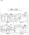
- FIG. 2 is a graph showing various characteristics related to the filter (first filter) of the first embodiment.
- FIG. 3 is a graph illustrating various characteristics related to the filter (first filter) of the second embodiment.
- FIG. 4 is a graph showing various characteristics related to the filter (first filter) of the third embodiment.
- FIG. 5 is a graph showing various characteristics related to the filter (first filter) of the fourth embodiment.
- FIG. 6 is a graph showing various characteristics related to the filter (first filter) of Comparative Example 1.
- FIG. 7 is a graph showing various characteristics related to the filter (first filter) of Comparative Example 2.
- FIG. 8 is a graph comparing various characteristics of the filters according to Comparative Example 1 and Comparative Example 2.
- FIG. 9 is a graph comparing various characteristics of the filters according to Example 1 and Comparative Example 2.
- FIG. 10 is a graph comparing various characteristics of the filters according to Example 2 and Comparative Example 2.
- FIG. 11 is a graph comparing various characteristics of the filters according to Example 3 and Comparative Example 2.
- FIG. 12 is a graph comparing various characteristics of the filters according to Example 4 and Comparative Example 2.
- FIG. 13 is a circuit block diagram of a multiplexer according to a modification of the first embodiment.
- FIG. 14 is a graph illustrating various characteristics related to the multiplexer according to the fifth embodiment.
- FIG. 15 is a graph illustrating various characteristics related to the multiplexer according to the sixth embodiment.
- FIG. 16 is a graph illustrating various characteristics related to the multiplexer according to the seventh embodiment.
- FIG. 17 is a graph illustrating various characteristics related to the multiplexer according to the eighth embodiment.
- 18A is a plan view and a cross-sectional view illustrating an electrode structure of an acoustic wave resonator according to Embodiment 1.
- FIG. 18B is a cross-sectional view of the electrode finger of the acoustic wave resonator and the surrounding structure in the first embodiment and its modification.
- FIG. 19 is a graph showing the relationship between the film thickness of the first adjustment film (Ksaw adjustment film) constituting the electrode structure and the impedance of the acoustic wave resonator.
- FIG. 1 is a plan view and a cross-sectional view illustrating an electrode structure of an acoustic wave resonator according to Embodiment 1.
- FIG. 18B is a cross-sectional view of the electrode finger of the acoustic wave resonator and the surrounding structure in the first embodiment and its modification.
- FIG. 19 is a graph showing the relationship between the
- FIG. 20 is a graph showing the relationship between the film thickness of the first adjustment film and the resonance frequency, antiresonance frequency, and specific bandwidth of the acoustic wave resonator.
- FIG. 21 is a graph showing the relationship between the film thickness of the second adjustment film constituting the electrode structure and the impedance of the acoustic wave resonator.
- FIG. 22 is a graph showing the relationship between the film thickness of the second adjustment film and the resonance frequency, antiresonance frequency, and specific bandwidth of the acoustic wave resonator.
- FIG. 23 is a circuit configuration diagram of a filter (first filter) according to the second embodiment.
- FIG. 24A is a diagram illustrating an equivalent circuit model of a resonator and a resonance characteristic thereof.
- FIG. 24B is a diagram illustrating an equivalent circuit model and its resonance characteristics when an impedance element is connected in series to the resonator.
- FIG. 24C is a diagram illustrating an equivalent circuit model of two resonators connected in parallel and a resonance characteristic thereof.
- FIG. 25 is a graph showing impedance characteristics of the series arm circuit of the filter (first filter) according to the second embodiment.
- FIG. 26 is a graph showing filter characteristics and impedance characteristics of the filter (first filter) according to the second embodiment.
- FIG. 27 is a circuit configuration diagram of a filter (first filter) according to the first modification of the second embodiment.
- FIG. 28 is a graph showing various characteristics of the filter according to the first modification of the second embodiment when the switch is on and when it is off.
- FIG. 29 is a circuit configuration diagram of a filter (first filter) according to the second modification of the second embodiment.
- FIG. 30 is a graph showing various characteristics of the filter according to the second modification of the second embodiment when the switch is on and when it is off.
- FIG. 31 is a circuit configuration diagram of a filter (first filter) according to the third modification of the second embodiment.
- FIG. 32 is a graph showing various characteristics of the filter according to the third modification of the second embodiment when the switch is on and when it is off.
- FIG. 33 is a circuit configuration diagram of a filter according to the third embodiment.
- FIG. 34A is a graph showing various characteristics of the filter according to Embodiment 3 in comparison between a case where the switch is on and a case where the switch is off.
- FIG. 34B is a graph illustrating impedance characteristics related to the series arm circuit in the third embodiment.
- FIG. 34C is a graph showing impedance characteristics relating to the parallel arm circuit in the third exemplary embodiment.
- FIG. 35 is a graph showing changes in filter characteristics when the switches are turned on and off individually in the third embodiment.
- FIG. 36A is a circuit block diagram of a multiplexer according to Embodiment 4.
- FIG. 36B is a plan view illustrating the structure of the filter according to Embodiment 4.
- FIG. 37 is a configuration diagram of a communication apparatus according to the fifth embodiment.
- circuit elements such as resonators can be appropriately adjusted according to required specifications. For this reason, the circuit elements may have different constants even if they have the same sign.
- “pass band low band end” means “the lowest frequency in the pass band”.
- “Passband high band end” means “the highest frequency in the passband”.
- “pass band lower band side” means “outside of the pass band and lower than the pass band (lower frequency side)”.
- the “passband high band side” means “outside the pass band and higher than the pass band (high frequency side)”.
- each switch is in a state where there is no capacitive component (that is, impedance is infinite) when it is off (that is, non-conductive), and when it is on (that is, when it is conductive), the resistance component is zero (that is, impedance is zero) Treat as an ideal switch.
- the resonance frequency in the resonator or circuit is a resonance frequency for forming an attenuation pole in the pass band of the filter including the resonator or the circuit or in the vicinity of the pass band unless otherwise specified.
- it is the frequency of a “resonance point” that is a singular point where the impedance of the circuit is minimized (ideally a point where the impedance is 0).
- the anti-resonance frequency in the resonator or circuit is an anti-resonance frequency for forming an attenuation pole near the passband or the passband of the filter including the resonator or the circuit, unless otherwise specified.
- This is the frequency of the “anti-resonance point”, which is a singular point where the impedance of the resonator or the circuit becomes maximum (ideally, the point where the impedance becomes infinite).
- the series arm circuit and the parallel arm circuit are defined as follows.
- the series arm circuit is configured such that, on a path connecting one input / output terminal and the other input / output terminal, one input / output terminal or the other input / output terminal and a node on the path to which the parallel arm circuit is connected. Arranged between a circuit arranged in between or one node on the path to which one parallel arm circuit is connected and another node on the path to which another parallel arm circuit is connected Circuit.
- the parallel arm circuit is a circuit arranged between one node on the path and the ground.
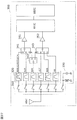
- FIG. 1 is a circuit block diagram of a multiplexer 1 according to the first embodiment. In the figure, the circuit configuration of the filter 10 is also shown.
- the multiplexer 1 includes a common terminal 110c, a filter 10 (first filter), and a filter 20 (second filter).
- the multiplexer 1 is a multiplexer for reception corresponding to a plurality of bands defined by 3GPP (Third Generation Partnership Project). Specifically, the reception band of Band12 (729-746 MHz) and Band13 Band12Rx + 13Rx, which is a reception band obtained by combining the reception bands (746-756 MHz) (hereinafter, may be simplified as “B12Rx + 13Rx”), and Band26Rx (hereinafter, “B26Rx”, which is the reception band of Band26 (859-894 MHz)) It may be simplified).
- Such a multiplexer 1 is used, for example, as a multiplexer compatible with LTE (Long Term Evolution).
- the multiplexer 1 is not limited to the reception multiplexer, and may be a multiplexer that supports both transmission and reception, such as a transmission multiplexer or a duplexer. Further, the number of filters included in the multiplexer 1 and the corresponding bands are not limited to the above.
- the filter 10 has an input / output terminal 110 (first input / output terminal) and an input / output terminal 120 (second input / output terminal).
- One input / output terminal 110 is connected to the common terminal 110 c of the multiplexer 1.
- This is an acoustic wave filter in which the other input / output terminal 120 is connected to the individual terminal 110a.
- the filter 10 is a reception filter corresponding to B12Rx + 13Rx, where B12Rx + 13Rx is a pass band, Band12Tx is a Band12 transmission band, and Band13Tx is a Band13 transmission band (hereinafter referred to as “B12Tx” and “B13Tx”, respectively). "May be simplified”) as an attenuation band.
- the filter 20 is a filter in which one input / output terminal 110 is connected to the common terminal 110 c of the multiplexer 1 and the other input / output terminal is connected to the individual terminal 110 b of the multiplexer 1, and has a higher frequency than the pass band of the filter 10. It has a passband on the side. Specifically, the frequency at the lower end of the pass band of the filter 20 is positioned higher than the frequency at the upper end of the pass band of the filter 10.
- the filter 20 is a reception filter corresponding to B26Rx, and B26Rx is used as a pass band, and Band26Tx which is the transmission band of Band26 (hereinafter, may be simplified as “B26Tx”) is used as an attenuation band. .
- the configuration of the filter 20 is not particularly limited, and an acoustic wave filter, an LC filter, a dielectric filter, or the like is appropriately used according to the required specifications of size and electrical characteristics.
- the input / output terminal 110 of the filter 10 and one input / output terminal of the filter 20 are directly or indirectly connected to the common terminal 110 c by the branch circuit 30. That is, the branch circuit 30 is a branch point (common connection point) of wiring, a switch or a phase shifter that can obtain one or more conductions, and one input / output terminal of each of the filters 10 and 20 is directly or Are connected to the common terminal 110c through a phase shifter or a switch.
- the filter 10 includes a serial arm circuit 11 provided on a path connecting the input / output terminal 110 (first input / output terminal) and the input / output terminal 120 (second input / output terminal), a node on the path, and a ground.
- a parallel arm circuit 12 connected to
- the frequency at which the impedance is minimum is defined as the resonance frequency
- the frequency at which the impedance is maximum is defined as the anti-resonance frequency
- the frequency at which the impedance of the resonator is minimum is defined as the resonance frequency.
- the frequency at which the impedance of the resonator is maximized is defined as the antiresonance frequency.
- the series arm circuit 11 is connected in parallel with the series arm resonator s1a (first series arm resonator) having a resonance frequency in the pass band of the filter 10 (first filter) and the series arm resonator s1a.
- a series arm resonator s1b (second series arm resonator) having a resonance frequency located on a higher frequency side than the frequency at the high end of the passband.
- the series arm resonator s1a is an elastic wave resonator connected between the input / output terminal 110 and the input / output terminal 120, and has a resonance frequency in the pass band of B12Rx + B13Rx in the present embodiment.
- the series arm resonator s1b is an elastic wave resonator connected in parallel with the series arm resonator s1a.
- the series arm resonator s1b is connected in parallel with the series arm resonator s1a without passing through other circuit elements.
- B12Rx + B13Rx has a resonance frequency higher (located on the high frequency side) than 756 MHz, which is the high band end of the passband.
- Each of the series arm resonators s1a and s1b may be constituted by a plurality of elastic wave resonators.
- the series arm resonators s1a and s1b are constituted by a plurality of divided resonators obtained by dividing one elastic wave resonator in series. It doesn't matter.
- the parallel arm circuit 12 has a resonance frequency located on the lower frequency side than the low pass end of the pass band of the filter 10 (first filter).
- the parallel arm resonator is a single elastic wave resonator. It consists only of p1. That is, in the present embodiment, the resonance frequency of the parallel arm circuit 12 is equal to the resonance frequency of the parallel arm resonator p1, and the parallel arm resonator p1 is lower than 729 MHz that is the lower end of B12Rx + B13Rx (positioned on the low frequency side). Have a resonant frequency. As a result, the steepness of the attenuation slope on the low pass band side of the filter 10 can be defined by the parallel arm resonator p1.
- the parallel arm resonator p1 may be configured by a plurality of elastic wave resonators, for example, a single elastic wave resonator may be configured by a plurality of divided resonators obtained by series division or the like.
- the configuration of the parallel arm circuit 12 is not limited to the parallel arm resonator using the elastic wave resonator as described above, and may be, for example, an LC resonance circuit, and is not limited to the resonance circuit. Or an impedance element such as a capacitance element may be used.
- the filter 10 configured as described above, it is possible to reduce the loss in the passband of another filter (here, the filter 20) that constitutes the multiplexer 1 together with the filter 10 that is an elastic wave filter. Details of this effect will be described later.
- Examples 1 to 4 have the configuration of the embodiment.
- the series arm resonator s1b has a resonance frequency located on the higher frequency side than the passband high band end of the filter 10.
- the comparative example 1 is different in that the series arm resonator s1b has a resonance frequency located on the lower frequency side than the high end of the pass band of the filter 10.
- the comparative example 2 is different in that the series arm resonator s1b is not provided. That is, in Comparative Example 2, the series arm circuit is composed of only the series arm resonator s1a.
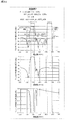
- Table 1 shows the circuit constants of the filters according to Examples 1 to 4 and Comparative Examples 1 and 2.
- the specific bandwidth (BWR) is a value obtained by dividing the frequency difference (fa ⁇ fr) between the anti-resonance frequency (fa) and the resonance frequency (fr) by the resonance frequency (fr) in the case of a single resonator.
- the anti-resonance frequency (fa1) located at the lowest frequency and the resonance frequency (at the lowest frequency) It is defined as a value ((fa1-fr1) / fr1) (or a percentage thereof) obtained by dividing the frequency difference (fa1-fr1) from fr1) by the resonance frequency (fr1) located at the lowest frequency.
- the series arm circuit or the parallel arm circuit has at least one resonance frequency and at least one anti-resonance frequency.
- the capacitance value here is a capacitance value of the acoustic wave resonator, and its definition will be described later.
- the parallel arm circuit has a resonance frequency frp at which the impedance
- the series arm circuit has a resonance frequency frs at which the impedance
- the antiresonance frequency fap of the parallel arm circuit and the resonance frequency frs of the series arm circuit are brought close to each other.
- an attenuation pole is formed at the resonance frequency frp where the impedance of the parallel arm circuit approaches a minimum, and the vicinity of the resonance frequency frp is a low-frequency-side blocking area.
- the impedance of the parallel arm circuit approaches the maximum near the anti-resonance frequency fap, and the impedance of the series arm circuit approaches the minimum near the resonance frequency frs.
- an attenuation pole is formed at the anti-resonance frequency fas where the impedance of the series arm circuit becomes high, and the vicinity of the anti-resonance frequency fas becomes a high-frequency side blocking region. That is, the passband is constituted by the anti-resonance frequency fap of the parallel arm circuit and the resonance frequency frs of the series arm circuit, and the attenuation pole on the low passband side is constituted by the resonance frequency frp of the parallel arm circuit.
- the anti-resonance frequency fas constitutes an attenuation pole on the high side of the passband.
- FIG. 2 is a graph showing various characteristics related to the filter of Example 1. Specifically, in the left column of the figure, from the top, the filter characteristics (pass characteristics), the impedance characteristics of the single resonator and the series arm circuit or parallel arm circuit, and the impedance characteristics in a wider band are shown. ing. The right column of the figure shows the reflection characteristics on the input / output terminal 110 side (that is, the common terminal 110c side). From the top, the reflection characteristics of the filter 10 alone (first filter alone), the resonator alone, and the resonance circuit The reflection characteristics as well as the reflection characteristics in a wider band are shown. The same applies to the following FIGS. 3 to 7.
- the characteristics of the filter 10 alone are obtained by eliminating the impedance matching deviation caused by disconnecting the filter other than the filter 10 (here, the filter 20) and the common terminal 110 c in the multiplexer 1. Characteristics.
- the frequency at the lower end of the pass band of the filter 10 (f L @ B12Rx + 13Rx) and the frequency at the upper end of the pass band of the filter 10 (f H @ B12Rx + 13Rx) satisfy the following first relationship.
- FIG. 3 is a graph showing various characteristics related to the filter of Example 2.
- the resonance frequency of the series arm resonator s1b (second series arm resonator) is lower than the passband low band end of the filter 20.
- the following second relation of being lower than the frequency (f L @ B26Rx) is satisfied.
- the specific bandwidth (BWR_s1b) of the series arm resonator s1b is equal to the specific bandwidth of the parallel arm circuit 12.
- the specific bandwidth of the parallel arm circuit 12 is equal to the specific bandwidth (BWR_p1) of the parallel arm resonator p1.
- the specific bandwidth (BWR_s1a) of the series arm resonator s1a is equal to the specific bandwidth of the parallel arm circuit 12. That is, in the first and second embodiments, the relationship between the specific bandwidths is as follows.
- BWR_s1a the specific bandwidth of the series arm resonator s1a and the specific bandwidth of the parallel arm circuit 12 (that is, BWR_p1) is not limited to the above, and may be different from each other.
- FIG. 4 is a graph showing various characteristics related to the filter of Example 3.
- Example 3 in addition to the first relationship, the third relationship is satisfied.
- FIG. 5 is a graph showing various characteristics related to the filter of Example 4.
- Example 4 in addition to the first and second relationships, the third relationship is satisfied.
- the filter 10 ideally has a reflection loss of 0 in the high frequency band of the pass band, but the reflection loss increases in the frequency band when the bulk wave loss increases. Therefore, when a multiplexer is configured by the filter 10 and the filter 20 having a higher passband than this, if the reflection loss of the frequency band of the filter 10 is large (bulk wave loss is large), the passband is located in the frequency band. Loss in the passband of the filter 20 is deteriorated.
- the series arm resonator s1b having a resonance frequency higher than the frequency at the high end of the pass band of the filter 10 is provided, so that the filter 20 In the frequency band corresponding to the band (pass band of the second filter, here B26Rx), the reflection loss of the series arm circuit 11 can be reduced more than the reflection loss of the series arm resonator s1a alone.
- the loss in the pass band of the filter 20 whose pass band is higher than the filter 10 can be reduced.
- the bulk wave loss due to the series arm resonator s1a occurs on the high frequency side of the antiresonance frequency, and the reflection loss increases.
- the resonance frequency (fr_s1a) of the series arm resonator s1a is located in the pass band of the filter 10
- the anti-resonance frequency (fa_s1a) is located outside the pass band of the filter 10, and specifically, the pass band. Located on the higher frequency side than the edge. For this reason, even if the bulk wave loss occurs, the characteristics in the pass band of the filter 10 are not affected.
- the filter 20 is located on the higher frequency side than the pass band of the filter 10, when applied to a multiplexer, the loss in the pass band can be deteriorated due to the influence of the bulk wave loss.
- the series arm resonator s1b since the series arm resonator s1b is connected in parallel to the series arm resonator s1a, the high-frequency signal input to the filter 10 is converted into the series arm resonator s1a and the series arm resonator s1b. Power distribution. Further, since the resonance frequency of the series arm resonator s1b is located higher than the passband high band end of the filter 10, the bulk wave loss due to the series arm resonator s1b is compared with the bulk wave loss due to the series arm resonator s1a. Occur at higher frequencies.
- the bulk wave loss in the frequency band corresponding to the pass band of the filter 20 when viewed as the entire series arm circuit 11 having the series arm resonator s1a and the series arm resonator s1b can be reduced. Loss in the passband can be reduced. That is, according to the present embodiment, the multiplexer 1 reduces the bulk wave loss in the frequency band corresponding to the passband of the filter 20 by the combined characteristics of the series arm resonator s1a and the series arm resonator s1b. Loss in the passband of the filter 20 having a passband higher than 10 can be reduced.
- FIG. 6 is a graph showing various characteristics related to the filter of Comparative Example 1.
- FIG. 7 is a graph showing various characteristics related to the filter of Comparative Example 2.
- FIG. 8 is a graph comparing various characteristics of the filters according to Comparative Example 1 and Comparative Example 2. Specifically, in the left column of the figure, the filter characteristic (passage characteristic) is shown in the upper part, and the impedance characteristic of the series arm circuit is shown in the lower part. The right column of the figure shows the reflection characteristic, the upper part shows the reflection characteristic of the single filter, and the lower part shows the reflection characteristic of the series arm circuit. This also applies to FIGS. 9 to 12 below.
- the series arm resonator s1b having a resonance frequency lower than the resonance frequency of the series arm resonator s1a is provided. Both the series arm resonator s1a and the series arm resonator s1b generate bulk wave loss. Therefore, the reflection loss in the frequency band corresponding to the pass band (B26Rx) of the filter 20 is deteriorated.
- Comparative Example 2 the reflection loss in the frequency band corresponding to the pass band of the filter 20 is reduced in Comparative Example 2 compared to Comparative Example 1 (2.3 dB in Comparative Example 1). In Comparative Example 2, 1.9 dB). That is, Comparative Example 2 is superior to Comparative Example 1 from the viewpoint of reducing the loss in the passband of the filter 20. Therefore, hereinafter, the effects achieved by the examples (Examples 1 to 4) will be described in comparison with Comparative Example 2.
- FIG. 9 is a graph comparing various characteristics of the filters according to Example 1 and Comparative Example 2.
- Example 1 As shown in the lower part of the left column in the figure, in Example 1, the series arm resonator s1b is connected in parallel to the series arm resonator s1a, so that the relative bandwidth of the series arm circuit is larger than that in Comparative Example 2. Narrow. For this reason, as shown in the upper part of the left column of the figure, in Example 1, the steepness of the attenuation slope on the high passband side is improved as compared with Comparative Example 2.
- the first embodiment in which the input high-frequency signal is power-distributed by the series arm resonator s1a and the series arm resonator s1b is compared with the comparative example 2 in which the power is not distributed.
- the bulk wave loss due to the series arm circuit 11 can be reduced.
- the reflection loss of the filter 10 in the frequency band corresponding to the filter 20 passband (B26Rx) can be reduced as compared with the second comparative example. (1.5 dB in Example 1 and 1.9 dB in Comparative Example 2).
- FIG. 10 is a graph comparing various characteristics of the filters according to Example 2 and Comparative Example 2.
- the series arm resonator s1b is connected in parallel to the series arm resonator s1a.
- the reflection loss of the filter 10 in the frequency band corresponding to the passband (B26Rx) of the filter 20 can be reduced.
- the resonance frequency of the series arm resonator s1b is lower than the frequency at the lower end of the pass band of the second filter.
- the capacitance of the acoustic wave resonator has a frequency characteristic, and specifically shows a high impedance capacity characteristic in the vicinity of the high frequency side of the antiresonance frequency.
- the capacitance of the series arm resonator s1b can be reduced in the passband (B26Rx) of the filter 20 as compared with the first embodiment, so that the impedance of the filter 10 viewed from the common terminal 110c can be reduced. Can be high. Therefore, the reflection loss of the filter 10 in the frequency band corresponding to the pass band (B26Rx) of the filter 20 can be further reduced (1.3 dB in the second embodiment and 1.5 dB in the first embodiment).
- the impedance of the series arm resonator s1b can be increased in the pass band of the filter 20
- the impedance of the filter 10 viewed from the common terminal 110c can be increased. Therefore, when the filter 10 is viewed from the common terminal 110c, the loss in the pass band of the filter 20 can be reduced by reducing the bulk wave loss in the frequency band corresponding to the pass band of the filter 20.
- FIG. 11 is a graph comparing various characteristics of the filters according to Example 3 and Comparative Example 2.
- an elastic wave resonator having a wide specific bandwidth is used as the series arm resonator s1a, so that it is combined with the series arm resonator s1b as compared with the first embodiment as shown in the lower row of the left column in FIG.
- the specific bandwidth of the series arm circuit 11 exhibiting the characteristics is narrowed to be approximately the same as the specific bandwidth of the comparative example 2. For this reason, as shown in the upper part of the left column in the figure, in Example 3, the steepness comparable to that of Comparative Example 2 is obtained for the attenuation slope on the high passband side.
- the filter 10 in the frequency band corresponding to the passband (B26Rx) of the filter 20 is compared with the second comparative example as shown in the upper part of the right column of FIG. Can be reduced (1.8 dB in Example 3, 1.9 dB in Comparative Example 2).
- FIG. 12 is a graph comparing various characteristics of the filters according to Example 4 and Comparative Example 2.
- an elastic wave resonator having a wide specific bandwidth is used as the series arm resonator s1a, so that the ratio of the series arm circuit 11 showing the combined characteristics with the series arm resonator s1b is obtained by the same operation as that of the third embodiment.
- the bandwidth becomes narrower and is comparable to the specific bandwidth of Comparative Example 2. For this reason, as shown in the upper part of the left column of the figure, in Example 4, the steepness comparable to that of Comparative Example 2 is obtained for the attenuation slope on the high passband side.
- the filter 10 in the frequency band corresponding to the passband (B26Rx) of the filter 20 is compared with the second comparative example as shown in the upper part of the right column in the same figure by the same operation as the first embodiment.
- the resonance frequency of the series arm resonator s1b is lower than the frequency at the lower end of the pass band of the filter 20 as compared with the third embodiment. For this reason, in the fourth embodiment, the reflection loss of the filter 10 in the frequency band corresponding to the pass band (B26Rx) of the filter 20 can be further reduced by the same operation as that of the second embodiment. (1.2 dB in Example 4, 1.8 dB in Example 3).
- an elastic wave resonator having a wide specific bandwidth is used as the series arm resonator s1a as compared with the first and second embodiments.
- the specific bandwidth of the circuit 11 is narrowed.
- the impedance of the series arm resonator s1b can be lowered compared to the first and second embodiments.
- power distribution to the series arm resonator s1b in which bulk wave loss is unlikely to occur in a frequency band corresponding to the pass band (B26Rx) of the filter 20 can be increased.
- the reflection loss in the frequency band corresponding to the pass band (B26Rx) of the filter 20 when viewed as a whole can be reduced. Therefore, the loss in the pass band of the filter 20 can be reduced.
- the series arm resonator s1b having a resonance frequency higher than the frequency at the high end of the passband of the filter 10 is provided as compared with the first and second comparative examples.
- the reflection loss can be reduced in a frequency band corresponding to the pass band of the filter 20.
- the resonance frequency of the series arm resonator s1b is higher than the frequency at the high end of the pass band of the filter 10 and lower than the pass band of the filter 20, the reflection loss in the frequency band corresponding to the pass band of the filter 20 is further reduced. it can.
- the specific bandwidth of the series arm resonator s1a is wider than the specific bandwidth of the parallel arm circuit 12, reflection loss in a frequency band corresponding to the passband of the filter 20 can be further reduced.
- Example 1 1.5 dB
- Example 2 1.3 dB
- Example 3 1.8 dB
- Example 4 1.2 dB Comparative Example 1 2.3 dB Comparative Example 2 1.9 dB
- FIG. 13 is a circuit block diagram of a multiplexer 1A according to a modification of the first embodiment. In the figure, the circuit configuration of the filter 10A is also shown.
- the filter 10A shown in the figure is an example of a specific circuit configuration of the filter 10.
- the filter 10A includes three series arm circuits 110s, 120s, 130s provided on a series arm connecting the input / output terminal 110 and the input / output terminal 120, and three parallel arm circuits 110p, 120p and 130p are provided.
- the serial arm circuit 110 s corresponds to the serial arm circuit 11 of the filter 10. That is, the filter 10A further includes another series arm circuit (series arm circuits 120s, 130s) having an acoustic wave resonator provided on the path connecting the input / output terminal 110 and the input / output terminal 120 to the filter 10. ).
- the parallel arm circuit 110 p corresponds to the parallel arm circuit 12 of the filter 10.
- the two series arm circuits 120s and 130s are each composed of only one series arm resonator s2 and s3, and the two parallel arm circuits 120p and 130p are composed only of one parallel arm resonator p2 and p3, respectively. Yes.
- the serial arm circuit 110s is connected to the input / output terminal 110 without passing through another series arm circuit (series arm circuit 120s, 130s), and the input / output terminal 110 is connected to the common terminal 110c without going through an elastic wave resonator. It is connected.
- the matching inductor 40 for impedance matching is provided, but this may not be required.
- Table 2 shows circuit constants of the filters (first filters) according to Examples 5 to 8 and Comparative Examples 3 and 4.
- FIG. 14 is a graph showing various characteristics relating to the multiplexer of the fifth embodiment.
- FIG. 15 is a graph illustrating various characteristics related to the multiplexer according to the sixth embodiment.
- FIG. 16 is a graph illustrating various characteristics related to the multiplexer according to the seventh embodiment.
- FIG. 17 is a graph illustrating various characteristics related to the multiplexer according to the eighth embodiment. Specifically, in these figures, the pass characteristic of the multiplexer, the filter characteristic of the filter unit corresponding to B12Rx + 13Rx (pass characteristic), and the reflection characteristic of the filter unit are shown in order from the top.
- the multiplexer pass characteristics include a pass characteristic of a path provided with a filter corresponding to B12Rx + 13Rx (hereinafter referred to as “B12Rx + 13Rx characteristic”) and a pass characteristic of a path provided with a filter compatible with B26Rx (hereinafter referred to as “ B26Rx characteristics ”).
- Table 3 shows loss in the pass band (I. Loss: Insertion Loss) and attenuation amount (Att .: Attention) in the B12Rx + 13Rx characteristics for the multiplexers according to Examples 5 to 8 and Comparative Examples 3 and 4.
- Table 4 shows loss in the passband and attenuation in the attenuation band (Att .: Attention) for the multiplexers according to Examples 5 to 8 and Comparative Examples 3 and 4.
- Table 5 shows the reflection loss (R. Loss: Return Loss) in the B26Rx band for the filter characteristics corresponding to B12Rx + 13Rx for the multiplexers according to Examples 5 to 8 and Comparative Examples 3 and 4.
- the series arm resonator s1b is connected in parallel to the series arm resonator s1a. Accordingly, the high-frequency signal input to the B12Rx + 13Rx-compatible filter 10A is power-distributed by the series arm resonator s1a and the series arm resonator s1b.
- the resonance frequency of the series arm resonator s1b is higher than the frequency (756 MHz) at the high end of the pass band of the filter corresponding to B12Rx + 13Rx.
- the series arm resonator s1b is less likely to generate bulk wave loss than the series arm resonator s1a. Therefore, the bulk wave loss in B26Rx when viewed as the whole series arm circuit can be reduced. Therefore, the loss in the pass band of the filter 20 can be reduced. That is, the loss in the passband can be reduced for the B26Rx characteristics of the multiplexer.
- the resonance frequency of the series arm resonator s1b is lower than the frequency (859 MHz) at the lower end of the pass band of the filter 20.
- the reflection loss in Examples 7 and 8 is worse than that in Examples 5 and 6.
- the capacitance of the series arm resonator s1b can be reduced in B26Rx, the impedance of the filter 10A viewed from the common terminal 110c can be increased. Therefore, the loss in the pass band can be reduced for the B26Rx characteristics of the multiplexer.
- the specific bandwidth of the series arm resonator s1a is wider than those of the fifth and sixth embodiments.
- the specific bandwidth of the series arm resonator s1a is set in series among one or more series arm circuits (here, three series arm circuits 110s, 120s, and 130s) included in the filter 10A. It is wider than any of the specific bandwidths of the series arm circuit and the parallel arm circuit (here, the series arm circuits 120s and 130s and the parallel arm circuits 110p, 120p, and 130p) different from the series arm circuit having the arm resonator s1a.
- the specific bandwidth of the series arm resonator s1a is equal to the series arm circuits 120s and 130s and the parallel arm circuit 110p. , 120p, 130p is preferably wider than any specific bandwidth. However, if the specific bandwidth of the series arm resonator s1a is wider than at least one specific bandwidth of the series arm circuits 120s and 130s and the parallel arm circuits 110p, 120p, and 130p, the loss is reduced as compared with the other configurations. be able to.
- the deterioration of the loss in the passband of the filter 20 due to the bulk wave loss of the filter 10A is caused by the series arm circuit connected to the closest common terminal 110c of the filter 10A (that is, the common terminal without passing through another series arm circuit).
- the series arm circuit 110s in which the series arm resonator s1b is connected in parallel to the series arm resonator s1a is connected to the common terminal 110c without passing through another series arm circuit. For this reason, when the filter 10A is viewed from the common terminal 110c, the bulk wave loss in the pass band of the filter 20 can be further reduced, so that the loss in the pass band of the filter 20 can be effectively reduced.
- Each acoustic wave resonator (each series arm resonator and each parallel arm resonator) included in the filters 10 and 10A according to the present embodiment and its modifications is an elastic wave using SAW (Surface Acoustic Wave). It is a resonator. Note that SAW includes not only surface waves but also boundary waves.
- FIG. 18A is a plan view and a cross-sectional view showing an electrode structure of an acoustic wave resonator in the first embodiment and its modification.
- FIG. 18B is a cross-sectional view of the electrode finger of the acoustic wave resonator and its surrounding structure in the first embodiment and its modification.
- 18A and 18B illustrate a schematic plan view and a schematic cross-sectional view showing the structure of an acoustic wave resonator res corresponding to each of the acoustic wave resonators constituting the filters 10 and 10A.
- the elastic wave resonator res shown in FIG. 18A is for explaining a typical structure of each of the elastic wave resonators, and the number and length of electrode fingers constituting the electrode are as follows. It is not limited to this.
- the acoustic wave resonator res has an IDT electrode 121 composed of a plurality of electrode fingers 121f formed on a substrate 101 having piezoelectricity at least partially.
- IDT electrode 121 composed of a plurality of electrode fingers 121f formed on a substrate 101 having piezoelectricity at least partially.
- the acoustic wave resonator res includes a substrate 101 having piezoelectricity, a Ksaw adjustment film 122, a protective layer 103, and a protective layer in addition to the IDT electrode 121. 104.
- the substrate 101 having piezoelectricity is made of lithium tantalate (LiTaO 3 ), lithium niobate (LiNbO 3 ), potassium niobate (KNbO 3 ), quartz, or a laminate thereof. With such a configuration, it is possible to configure an elastic wave resonator res that exhibits high Q and broadband characteristics.
- the substrate 101 having piezoelectricity may be a substrate having piezoelectricity at least partially.
- a piezoelectric thin film piezoelectric body
- the piezoelectric thin film may have a sound velocity different from that of the piezoelectric thin film and a laminated body such as a support substrate.
- the piezoelectric substrate 101 is, for example, a laminate including a high sound speed support substrate and a piezoelectric thin film formed on the high sound speed support substrate, a high sound speed support substrate, and a low sound speed formed on the high sound speed support substrate.
- a laminate including a film and a piezoelectric thin film formed on the low-sonic film, or a support substrate, a high-sonic film formed on the support substrate, a low-sonic film formed on the high-sonic film, A laminate including a piezoelectric thin film formed on a low acoustic velocity film may be used.
- the substrate 101 having piezoelectricity may have piezoelectricity in the entire substrate. In this case, the substrate 101 having piezoelectricity is composed of one piezoelectric layer.
- the IDT electrode 121 is composed of a pair of comb electrodes 121a and 121b facing each other.
- Each of the comb-shaped electrodes 121a and 121b includes a plurality of electrode fingers 121f that are parallel to each other and a bus bar electrode that connects the plurality of electrode fingers 121f.
- the plurality of electrode fingers 121f are formed along a direction orthogonal to the propagation direction.
- Reflectors are provided on both sides of the IDT electrode 121. The reflector may be configured by weighting, and the reflector may not be provided.
- the IDT electrode 121 is composed of a low density metal layer or a laminate of a low density metal layer and a high density metal layer.
- the low density metal layer is a metal layer composed of a low density metal selected from one or more of Al, Ti, Cu, Ag, Ni, Cr and alloys thereof, or a laminate of these metal layers.
- the high density metal layer is a metal layer composed of a high density metal selected from one or more of Au, Pt, Ta, Mo and W. Note that the low-density metal is not limited to the above material, and may be a metal having a lower density than the high-density metal constituting the high-density metal layer.
- the IDT electrode 121 shown in FIG. 18B includes a metal film 211 made of NiCr, a metal film 212 made of Pt, a metal film 213 made of Ti, and AlCu (alloy of Al and Cu) in order from the piezoelectric substrate 101 side.
- the metal film 214 made of Ti and the metal film 215 made of Ti are stacked. That is, the IDT electrode 121 is composed of a laminate of four metal films 211, 213, 214, and 215, each of which is a low-density metal layer, and one metal film 215 that is a high-density metal layer.
- the protective layer 103 and the protective layer 104 are protective layers for the purpose of protecting the IDT electrode 121 from the external environment, adjusting frequency temperature characteristics, and improving moisture resistance.
- the Ksaw adjustment film 122 is a first adjustment film that is formed between the piezoelectric substrate 101 and the IDT electrode 121 and adjusts the electromechanical coupling coefficient.
- the protective layers 103 and 104 and the Ksaw adjusting film 122 are made of silicon oxide (SiO 2 ), silicon nitride (SiN), aluminum nitride (AlN), or a laminate thereof.
- the protective layer 103 and the Ksaw adjusting film 122 are used.
- Is made of SiO 2 and the protective layer 104 is made of SiN.
- the protective layer 103 and the protective layer 104 together constitute a second adjustment film.
- the configuration of the IDT electrode 121 shown in FIG. 18B is an example, and is not limited thereto.
- the IDT electrode 121 may not be a laminated structure of metal films but may be a single layer of metal films.
- the material which comprises each metal film and each protective layer is not limited to the material mentioned above.
- the IDT electrode 121 may be made of, for example, a metal or an alloy such as Ti, Al, Cu, Pt, Au, Ag, or Pd, and is made of a plurality of laminates made of the above metals or alloys. May be.
- the configurations of the protective layers 103 and 104 and the Ksaw adjusting film 122 are not limited to the above-described configurations, and include, for example, a dielectric or an insulator such as SiO 2 , SiN, AlN, polyimide, or a laminate thereof. It doesn't matter. Further, the protective layers 103 and 104 and the Ksaw adjustment film 122 may not be provided.
- the wavelength of the excited elastic wave is defined by the design parameters of the IDT electrode 121 and the like.
- the wavelength of the elastic wave is defined by the repetition period ⁇ of the electrode finger 121f connected to one bus bar electrode among the plurality of electrode fingers 121f.
- the electrode finger pitch (pitch of the plurality of electrode fingers 121f, that is, the electrode finger cycle) P is 1 ⁇ 2 of the repetition cycle ⁇
- the line width of the electrode fingers 121f is W
- the crossing width A of the IDT electrode 121 is an overlapping electrode when the electrode finger 121f connected to one of the pair of bus bar electrodes and the electrode finger 121f connected to the other are viewed from the propagation direction of the elastic wave.
- the finger length is an overlapping electrode when the electrode finger 121f connected to one of the pair of bus bar electrodes and the electrode finger 121f connected to the other are viewed from the propagation direction of the elastic wave.
- the electrode duty is the line width occupation ratio of the plurality of electrode fingers 121f, and the ratio of the line width to the added value of the line width and the space width of the plurality of electrode fingers 121f, that is, W / ( W + S). That is, the electrode duty is defined by the ratio of the width of the plurality of electrode fingers 121f to the electrode finger pitch (the pitch of the plurality of electrode fingers 121f), that is, W / P.
- the number of pairs is the number of electrode fingers 121f making a pair, and is defined by (total number of electrode fingers 121f ⁇ 1) / 2.
- the film thickness T of the IDT electrode 121 (that is, the film thickness of the plurality of electrode fingers 121f) is the total film thickness of the metal films 211 to 215. Further, the capacitance C 0 of the acoustic wave resonator res is expressed by the following formula 1.
- ⁇ 0 is a dielectric constant in vacuum
- ⁇ r is a dielectric constant of the substrate 101 having piezoelectricity
- FIG. 19 is a graph showing the relationship between the film thickness of the first adjustment film (Ksaw adjustment film) constituting the electrode structure and the impedance of the acoustic wave resonator.
- FIG. 20 is a graph showing the relationship between the film thickness of the first adjustment film and the resonance frequency, antiresonance frequency, and specific bandwidth of the acoustic wave resonator.
- FIG. 19 shows the frequency characteristics of the impedance of the acoustic wave resonator when the thickness of the first adjustment film shown in FIG. 18B is changed.
- a ⁇ 10 ° Y-cut LiNbO 3 substrate was used as the piezoelectric substrate 101, and the IDT electrode film thickness was 595 nm.
- FIG. 20 shows the relationship between the film thickness of the first adjustment film and the resonance frequency fr.
- the middle part of FIG. 20 shows the film thickness of the first adjustment film and the anti-resonance frequency fa. The relationship is shown, and the lower part of FIG. 20 shows the relationship between the film thickness of the first adjustment film and the specific bandwidth BWR.
- the anti-resonance frequency fa hardly moves and the resonance frequency fr shifts. More specifically, as shown in FIG. 20, as the thickness of the first adjustment film increases, the resonance frequency fr shifts to the higher frequency side, and the specific bandwidth BWR decreases.
- the configuration is such that the specific bandwidth of the series arm resonator s1a is wider than the specific bandwidth of at least one other acoustic wave resonator.
- the first adjustment film on the IDT electrode of the series arm resonator s1a is made thinner than the first adjustment film on the IDT electrode of at least one other elastic wave resonator, or (2) the series arm resonator The first adjustment film is not formed on the IDT electrode of s1a.
- FIG. 21 is a graph showing the relationship between the film thickness of the second adjustment film constituting the electrode structure and the impedance of the acoustic wave resonator.
- FIG. 22 is a graph showing the relationship between the film thickness of the second adjustment film and the resonance frequency, antiresonance frequency, and specific bandwidth of the acoustic wave resonator.
- FIG. 21 shows the frequency characteristics of the resonance impedance of the acoustic wave resonator when the thickness of the second adjustment film (protective layer 103 + 104) shown in FIG. 18B is changed.
- a ⁇ 10 ° Y-cut LiNbO 3 substrate was used as the piezoelectric substrate 101, and the IDT electrode film thickness was 595 nm.
- FIG. 22 shows the relationship between the film thickness of the second adjustment film and the resonance frequency fr.
- the middle part of FIG. 22 shows the film thickness of the second adjustment film and the anti-resonance frequency fa. The relationship is shown, and the lower part of FIG. 22 shows the relationship between the film thickness of the second adjustment film and the specific bandwidth BWR.
- the anti-resonance frequency fa and the resonance frequency fr are shifted. More specifically, as shown in FIG. 22, the resonance frequency fr shifts to the higher frequency side and the antiresonance frequency fa shifts to the lower frequency side as the thickness of the second adjustment film is increased.
- the specific bandwidth BWR is reduced.
- the configuration is such that the specific bandwidth of the series arm resonator s1a is wider than the specific bandwidth of at least one other acoustic wave resonator.
- the first adjustment film and the second adjustment film may be appropriately set according to the required filter characteristics.
- the second adjustment film since the second adjustment film also has a function of increasing frequency temperature characteristics and moisture resistance, it is set in consideration of the frequency temperature characteristics and moisture resistance necessary for the required filter, and the specific bandwidth This adjustment may be determined mainly by the presence / absence of the first adjustment film and the film thickness.
- the series arm circuit of the first filter has a configuration in which a series arm resonator s1a (first series arm resonator) and a series arm resonator s1b (first series arm resonator) are connected in parallel.
- the series arm circuit of the first filter has a configuration in which another circuit element is added to the above configuration.
- FIG. 23 is a circuit configuration diagram of a filter 10B (first filter) according to the second embodiment.
- the filter 10B shown in the figure includes a series arm circuit 11B and a parallel arm circuit 12, and the series arm circuit 11B includes a series arm resonator s1a, a series arm resonator s1b, and an impedance element z1.
- the filter 10B shown in the figure differs from the filter 10 according to the first embodiment only in having an impedance element z1.
- the filter 10B according to the present embodiment will be described focusing on differences from the filter 10 according to the first embodiment.
- the series arm resonator s1a (first series arm resonator) is connected between the input / output terminal 110 and the input / output terminal 120, and has an acoustic wave resonance having a resonance frequency in the pass band of the filter 10B (first filter). It is a child.
- the impedance element z1 is a first impedance element connected in series to the series arm resonator s1a, and is exemplified by a capacitor or an inductor.
- the series arm resonator s1b (second series arm resonator) is connected in parallel to a circuit in which the series arm resonator s1a and the impedance element z1 are connected in series, and is located on the higher frequency side than the passband high band end of the filter 10B.
- An elastic wave resonator having a resonance frequency.
- the pass band of another filter (here, the filter 20) that configures the multiplexer 1 together with the filter 10 that is an acoustic wave filter.
- the loss inside can be reduced.
- the pass band or the attenuation band can be adjusted by appropriately selecting the impedance element.
- the impedance element may be capable of adjusting the element value, such as a variable capacitor such as a varicap and DTC (Digitally Tunable Capacitor).
- FIG. 24A is a diagram illustrating an equivalent circuit model of one resonator and its resonance characteristics.
- the resonator includes a circuit connected to the capacitor C 1 and the inductor L 1 in series, the capacitor C 0 is in parallel to the circuit connected in series with a capacitor C 1 and the inductor L 1 It can be represented by a connected circuit (parallel connection circuit).
- the capacitor C 0 is the capacitance of the resonator.
- the resonance frequency fr of the resonator is defined by a circuit in which the capacitor C 1 and the inductor L 1 are connected in series, and is the frequency at which the impedance of the equivalent circuit becomes zero. Is expressed by Equation 3.
- Equation 4 is obtained by solving Equation 4.
- the anti-resonance frequency fa appears on the higher frequency side than the resonance frequency fr.
- the resonator has one resonance frequency and one anti-resonance frequency positioned higher than the resonance frequency.
- the resonator includes a circuit connected to the capacitor C 1 and the inductor L 1 in series, a capacitor C 0 in parallel with the circuit connected to the capacitor C 1 and the inductor L 1 in series It can be represented by a connected circuit.
- the capacitor C 0 is the capacitance of the resonator.
- a parallel circuit of the impedance element X 1 and the switch SW is connected.
- the resonance characteristics of the equivalent circuit will be described for the case where the switch SW is on. If the switch SW is on, the impedance element X 1 becomes a short circuit, the resonance frequency fr_on and anti-resonance frequency fa_on, respectively, becomes the same as the resonant frequency fr and the antiresonant frequency fa of the resonator alone in FIG. 24A, the formula 6 And represented by Equation 7.
- the impedance elements X 1 be a capacitor, and will be described separately in the case of (2) the impedance element X 1 is an inductor.
- the anti-resonance frequency fa_off1 when the switch SW is off is the same as the anti-resonance frequency fa_on when the switch SW is on, and is expressed by Expression 10.
- Equation 6 Equation 7, Equation 9 and Equation 10
- the impedance element X 1 is a capacitor, as shown in the right graph of FIG. 24B, regardless of the changeover of the switch SW on and off, the anti-resonance frequency fa_on And fa_off1 match.
- the resonance frequency shifts to a higher frequency side when the switch SW is off (fr_off1) than when the switch SW is on (fr_on).
- fr_off2L is a resonance frequency on the low frequency side when the switch SW is off
- fr_off2H is a resonance frequency on the high frequency side when the switch SW is off.
- the anti-resonance frequency fa_off2 when the switch SW is off is the same as the anti-resonance frequency fa_on when the switch SW is on, and is expressed by Expression 13.
- Impedance element X 1 is the case of the capacitor Ct has a configuration in which capacitor Ct in the capacitor C 0 in the equivalent circuit model shown in FIG. 24A are connected in parallel. Therefore, the resonance frequency in this case is represented by an expression in which C 0 in Expression 6 is replaced with a combined capacitance (C 0 + Ct) of the capacitor C 0 and the capacitor Ct, and matches the resonance frequency of the single resonator. I understand that. Further, it can be seen from Equation 7 that the antiresonance frequency in this case shifts to a lower frequency side than the antiresonance frequency of the single resonator.
- FIG. 24C is a diagram illustrating an equivalent circuit model of two resonators connected in parallel and a resonance characteristic thereof.
- the figure shows a model in which the resonators res1 and res2 are connected in parallel.
- Resonator res1 the table in the circuit connecting the capacitor C 01 in parallel to the circuit connecting the capacitor C 1 and the inductor L 1 in series, the circuit connected in series with a capacitor C 1 and the inductor L 1 is
- resonator res2 has a capacitor C 2 and the inductor L 2 and the circuit connected in series, and a capacitor C 2 and the inductor L 2 in the circuit connecting the capacitor C 02 in parallel to the circuit connected in series Can be represented.
- the capacitors C 01 and C 02 are the capacitances of the resonators res1 and res2, respectively.
- a circuit in which the resonator res1 and the resonator res2 are connected in parallel is represented by an equivalent circuit shown in the lower left of FIG. 24C.
- the two resonance frequencies are defined, the resonance frequency fr1, fr2, respectively, the circuit connecting the capacitor C 1 and the inductor L 1 in series, and, a capacitor C 2 and the inductor L 2 in series It is defined by the resonant frequency of the connected circuit and is shown in Equation 14.
- the two resonance frequencies fr1 and fr2 represented by the equivalent circuit are equal to the resonance frequency fr_res1 of the resonator res1 and the resonance frequency fr_res2 of the resonator res2, respectively.
- the anti-resonance frequency of the equivalent circuit is a frequency at which the admittance Y of the equivalent circuit becomes 0, by solving Equation 15, two anti-resonance frequencies (fa1, fa2) are obtained as shown in Equation 16. I understand that I have it.
- the anti-resonance frequencies fa1 and fa2 obtained by the above equation 15 are different from the anti-resonance frequencies of the single resonator obtained by the equation 4 (shown as fa_res1 and fa_res2 in the graph of FIG. 24C). Further, the antiresonance frequency fa1 derived from Expression 15 is lower than the antiresonance frequency fa_res1 of the resonator res1 alone, and the antiresonance frequency fa2 is lower than the antiresonance frequency fa_res2 of the resonator res2 alone.
- Equations 23 and 24 are obtained by solving Equations 21 and 22.
- FIG. 25 is a graph showing impedance characteristics of the series arm circuit 11B of the filter 10B (first filter) according to the second embodiment.
- the upper part of the figure shows the resonance characteristics when the impedance element z1 is a capacitor, and the lower part shows the resonance characteristics when the impedance element z1 is an inductor.
- the circuit constants of the filter 10B (first filter) at this time are the same as the circuit constants of the filter (first filter) of Example 2 described in the first embodiment. That is, the characteristic of the series arm circuit 11B when the impedance element z1 is not present is equal to the characteristic of the series arm circuit in the second embodiment.
- the resonance frequency of the series arm circuit 11B is expressed by the above equations 23 and 24, and the resonance frequency (fr1) on the low frequency side is the capacitance value of the capacitor.
- the anti-resonance frequency is omitted because the derivation of the above equation is complicated, but the anti-resonance frequency (fa1) on the low frequency side slightly shifts to the high frequency side as the capacitance value of the capacitor decreases.
- the antiresonance frequency (fa2) on the side shifts to the higher frequency side as the capacitance value of the capacitor decreases.
- the frequency difference (fa1-fr1) between the anti-resonance frequency (fa1) on the low frequency side and the resonance frequency (fr1) on the low frequency side is the resonance frequency (fr1) on the low frequency side.
- the specific bandwidth (BWR1) on the low frequency side defined as the value divided by ((fa1-fr1) / fr1) (or its percentage) becomes significantly smaller as the capacitance value of the capacitor becomes smaller.
- the frequency difference (fa2-fr2) between the anti-resonance frequency (fa2) on the high frequency side and the resonance frequency (fr2) on the high frequency side is set to the resonance frequency (fr2) on the high frequency side.
- the specific bandwidth (BWR2) on the high frequency side defined as a value divided by ((fa2-fr2) / fr2) (or a percentage thereof) increases as the capacitance value of the capacitor decreases.
- Table 6 shows a series arm circuit in which the impedance element z1 is a capacitor, a low frequency side resonance frequency (fr1), a low frequency side anti-resonance frequency (fa1), a low frequency side specific bandwidth (BWR1), The resonance frequency (fr2) on the high frequency side, the anti-resonance frequency (fa2) on the high frequency side, and the specific bandwidth (BWR2) on the high frequency side are shown.
- the capacitance value of the capacitor is 16 pF is omitted for the sake of simplicity, but Table 6 also shows the numerical values in this case.
- ⁇ in the “capacitance value” column of Table 6, there is shown a numerical value of a series arm circuit in the case where there is no capacitor, that is, only a resonator.
- the resonance frequency (fr1) on the low frequency side has a large inductance value of the inductor.
- the anti-resonance frequency (fa1) on the low frequency side slightly shifts to the low frequency side as the inductance value of the inductor increases, and the anti-resonance frequency (fa2) on the high frequency side decreases toward the low frequency side as the inductance value of the inductor increases. shift.
- the specific bandwidth (BWR1) on the low frequency side of the series arm circuit 11B increases significantly as the inductance value of the inductor increases.
- the high frequency side specific bandwidth (BWR2) decreases as the inductance value of the inductor increases.
- Table 7 shows the resonance frequency (fr1) on the low frequency side, the anti-resonance frequency (fa1) on the low frequency side, the specific bandwidth (BWR1) on the low frequency side for the series arm circuit when the impedance element z1 is an inductor.
- the resonance frequency (fr2) on the high frequency side, the anti-resonance frequency (fa2) on the high frequency side, and the specific bandwidth (BWR2) on the high frequency side are shown.
- the impedance value of the inductor is 2 nH is omitted for the sake of simplicity, but Table 7 also shows the numerical values in this case.
- the item “ ⁇ ” in the “Inductance value” column of Table 7 shows the numerical value of the series arm circuit without the inductor, that is, the series arm circuit including only the resonator.
- FIG. 26 is a graph showing the filter characteristics and impedance characteristics of the filter (first filter) according to the second embodiment.
- the pass characteristics (filter characteristics) when there is no impedance element z1 when the impedance element z1 is a capacitor with a capacitance value of 8 pF, and when the impedance element z1 is an inductor with an inductance value of 4 nH are shown.
- the series arm circuit 11B and the parallel arm circuit 12 that is, The resonance characteristic (impedance characteristic) of the parallel arm resonator p1 is shown.
- circuit constants of the filter 10B (first filter) at this time are the same as the circuit constants of the filter (first filter) of Example 2 described in the first embodiment. That is, the characteristics when the impedance element z1 is not present are equal to the characteristics of the second embodiment.
- the filter 10B As described above, due to the configuration of the impedance element z1, the specific bandwidth of the series arm circuit 11B changes, and particularly, the specific bandwidth on the low frequency side changes remarkably. Thereby, in the filter 10B, the steepness of the attenuation slope on the high pass band side can be adjusted. Specifically, in the present embodiment, as shown in the lower part of the figure, the passband width is adjusted by adjusting the anti-resonance frequency on the low frequency side of the series arm circuit 11B to a predetermined frequency. ing. The resonance frequency on the low frequency side of the series arm circuit 11B may be adjusted to a predetermined frequency. In this case, the attenuation band is adjusted. That is, according to the filter 10B according to the present embodiment, the steepness of the attenuation slope on the high passband side can be adjusted by appropriately selecting the impedance element, so that the passband width or attenuation band is adjusted. It becomes possible.
- FIG. 27 is a circuit configuration diagram of a filter 10C according to the first modification of the second embodiment.
- the filter 10C shown in the figure includes a series arm circuit 11C and a parallel arm circuit 12, and the series arm circuit 11C includes a series arm resonator s1a, a series arm resonator s1b, and a switch SW1.
- the filter 10C shown in the figure differs from the filter 10B according to the second embodiment only in that the impedance element z1 is a capacitor and further has a switch SW1.
- the filter 10C according to this modification will be described focusing on differences from the filter 10B according to the second embodiment.
- the series arm resonator s1a (first series arm resonator) is connected between the input / output terminal 110 and the input / output terminal 120, and has an acoustic wave resonance having a resonance frequency in the pass band of the filter 10C (first filter). It is a child.
- the series arm resonator s1b (second series arm resonator) is connected in parallel to a circuit in which the series arm resonator s1a and the impedance element z1 are connected in series, and is located on the higher frequency side than the passband high band end of the filter 10C.
- An elastic wave resonator having a resonance frequency.
- the switch SW1 is a first switch connected in series with the series arm resonator s1b.
- the filter 10C configured as described above switches the frequency of the passband and the frequency of the attenuation pole by switching the switch SW1 on and off according to a control signal from a control unit (not shown) such as an RFIC ( Variable).
- a control unit such as an RFIC ( Variable).
- control unit turns on or off the switch SW1 in an environment where Band-A is used, and sets the switch SW1 on the other of on and off in an environment where Band-B is used. That is, for the switch SW1, either on or off is selected under a certain environment, and the on / off of the switch SW1 is fixed (invariable) under the environment.
- FIG. 28 is a graph showing various characteristics of the filter 10C according to the first modification of the second embodiment when the switch SW1 is on and when it is off.
- the upper row of the left column of the figure shows the pass characteristic of the filter 10C with respect to the on / off state of the switch SW1
- the lower row of the left column shows the series arm circuit 11C and the parallel arm with respect to the on / off state of the switch SW1.
- the resonance characteristics of the circuit 12 are shown.
- the passband of the graph shown in the left column and the characteristics in the vicinity thereof are enlarged.
- circuit constant of the filter 10C (first filter) at this time is the same as the circuit constant of the filter (first filter) of Example 2 described in the first embodiment.
- the capacitance value of the impedance element z1 (capacitor here) is 8 pF.
- the filter 10C when the switch SW1 is turned on, the series arm resonator s1b is connected in parallel to the circuit in which the series arm resonator s1a and the impedance element z1 are connected in series. Therefore, the high-frequency signal input to the filter 10C is power-distributed by the series arm resonator s1a, the impedance element z1, and the series arm resonator s1b. Therefore, according to the filter 10C according to this modification, the bulk wave loss in the frequency band corresponding to the pass band of the filter 20 (second filter) is reduced by the combined characteristics of the series arm resonators s1a and s1b and the impedance element z1. Therefore, the reflection loss in the frequency band can be reduced.
- the anti-resonance frequency on the low frequency side of the series arm circuit 11C is shifted to the high frequency side as shown in FIG.
- the anti-resonance frequency constitutes an attenuation pole on the high side of the pass band of the filter 10C, the frequency at the high end of the pass band and the attenuation on the high side of the pass band according to switching of the switch SW1 on and off.
- the frequency of the pole can be varied.
- the loss in the passband of the filter 20 (second filter) can be reduced by turning on the switch SW1. Therefore, when the Band corresponding to the pass band of the filter 20 (in this case, B26Rx) is selected in the multiplexer (that is, when the filter 20 is selected), the switch SW1 of the filter 10C is turned on. The loss in the passband of the filter 20 can be reduced to improve performance. Further, according to the present modification, the frequency of the pass band and the frequency of the attenuation pole of the filter 10C (first filter) can be varied according to the on / off state of the switch SW1. Therefore, a multiplexer corresponding to a larger number of bands can be realized.
- the frequency and attenuation band of the passband of the filter 10C (first filter) can be varied while reducing the loss in the passband of the filter 20 (second filter).
- a low-loss multiplexer corresponding to the band can be realized.
- Such an effect is the same even when the impedance element z1 is not provided. For this reason, the impedance element z1 may not be provided in the filter 10C.
- FIG. 29 is a circuit configuration diagram of a filter 10D according to the second modification of the second embodiment.
- the filter 10D shown in the figure includes a series arm circuit 11D and a parallel arm circuit 12, and the series arm circuit 11D includes a series arm resonator s1a, a series arm resonator s1b, an impedance element z1, and a switch SW2. Is provided.
- the filter 10D shown in the figure differs from the filter 10B according to the second embodiment only in that the impedance element z1 is a capacitor and further has a switch SW2.
- the filter 10D according to the present modification will be described focusing on differences from the filter 10B according to the second embodiment.
- the series arm resonator s1a (first series arm resonator) is connected between the input / output terminal 110 and the input / output terminal 120, and has an acoustic wave resonance having a resonance frequency in the pass band of the filter 10D (first filter). It is a child.
- the series arm resonator s1b (second series arm resonator) is connected in parallel to a circuit in which the series arm resonator s1a and the impedance element z1 are connected in series, and is located on the higher frequency side than the passband high band end of the filter 10D.
- An elastic wave resonator having a resonance frequency.
- the impedance element z1 is a first impedance element connected in series to the series arm resonator s1a.
- the switch SW2 is a second switch connected in parallel to the impedance element z1.
- the filter 10D configured as described above changes the frequency of the pass band or the frequency of the attenuation pole by switching the switch SW2 on and off in accordance with a control signal from a control unit (not shown) such as an RFIC. be able to.
- a control unit such as an RFIC.
- FIG. 30 is a graph showing the pass characteristics and impedance characteristics of the filter 10D according to the second modification of the second embodiment. Specifically, the upper stage of the left column of the figure shows the pass characteristic of the filter 10D with respect to the on / off of the switch SW2, and the lower stage of the left column shows the series arm circuit 11D and the parallel arm with respect to the on / off of the switch SW2. The resonance characteristics of the circuit 12 are shown. In the right column of the figure, the passband of the graph shown in the left column and the characteristics in the vicinity thereof are enlarged.
- circuit constants of the filter 10D (first filter) at this time are the same as the circuit constants of the filter (first filter) of Example 2 described in the first embodiment.
- the capacitance value of the impedance element z1 (capacitor here) is 8 pF.
- the switch SW2 when the switch SW2 is turned on, the impedance element z1 is short-circuited by the switch SW2, so that the circuit configuration is the same as that of the filter 10 of the first embodiment, and the passage shown in FIG.
- the characteristics and resonance characteristics are the same as those of the second embodiment shown in FIG. That is, when the switch SW2 is turned on, the bulk wave loss in the frequency band corresponding to the pass band of the filter 20 (second filter) is reduced by the combined characteristics of the series arm resonators s1a and s1b and the impedance element z1. Therefore, the reflection loss in the frequency band corresponding to the pass band of the filter 20 can be reduced.
- the circuit configuration is the same as that of the filter 10B according to the second embodiment (impedance element z1 is a capacitor).
- the pass characteristics and the resonance characteristics are also shown in FIG. This is the same as the characteristic (z1: capacitor) of the illustrated second embodiment. That is, as compared with the case where the switch SW2 is in the ON state, the resonance frequency on the low frequency side of the series arm circuit 11D is shifted to the high frequency side as shown in the lower part of FIG. In this regard, since the resonance frequency constitutes the passband of the filter 10D, the frequency at the high end of the passband can be varied in accordance with switching of the switch SW2 on and off.
- the high-frequency signal input to the filter 10D is distributed by the series arm resonator s1a, the impedance element z1, and the series arm resonator s1b. Therefore, even in this case, the reflection loss in the frequency band corresponding to the passband of the filter 20 can be reduced by reducing the bulk wave loss due to the combined characteristics of the series arm resonators s1a and s1b and the impedance element z1. .
- loss in the passband of the filter 20 can be reduced regardless of whether the switch SW2 is on or off.
- the frequency of the high end of the pass band of the filter 10D (first filter) can be varied according to the switching on and off of the switch SW2.
- the frequency at the high band end of the pass band of the filter 10D (first filter) can be varied while reducing the loss in the pass band of the filter 20 (second filter).
- FIG. 31 is a circuit configuration diagram of a filter 10E according to the third modification of the second embodiment.
- the filter 10E shown in the figure includes a series arm circuit 11E and a parallel arm circuit 12, and the series arm circuit 11E includes a series arm resonator s1a, a series arm resonator s1b, an impedance element z1, and a switch SW1. SW2.
- the filter 10E shown in the figure is different from the filter 10B according to the second embodiment only in that the impedance element z1 is a capacitor and further includes switches SW1 and SW2.
- the filter 10E according to this modification will be described focusing on differences from the second embodiment.
- the series arm resonator s1a (first series arm resonator) is connected between the input / output terminal 110 and the input / output terminal 120, and has an acoustic wave resonance having a resonance frequency in the pass band of the filter 10E (first filter). It is a child.
- the series arm resonator s1b is a second series arm resonator connected to the series arm resonator s1a.
- the switch SW1 is a first switch connected in series to the series arm resonator s1b.
- the switch SW2 is a second switch connected in parallel to the impedance element z1.
- FIG. 32 is a graph showing the pass characteristics and impedance characteristics of the filter 10E according to the third modification of the second embodiment. Specifically, the upper stage of the left column of the figure shows the pass characteristics of the filter 10E with respect to the on and off of the switches SW1 and SW2, and the lower stage of the left column shows a series arm circuit for the on and off of the switches SW1 and SW2. The resonance characteristics of 11E and parallel arm circuit 12 are shown. In the right column of the figure, the passband of the graph shown in the left column and the characteristics in the vicinity thereof are enlarged.
- the circuit constant of the filter 10E (first filter) at this time is the same as the circuit constant of the filter (first filter) of Example 2 described in the first embodiment.
- the capacitance value of the impedance element z1 (capacitor here) is 8 pF.
- the circuit configuration when the switch SW1 is turned on and the switch SW2 is turned on, the circuit configuration is the same as that of the filter 10 according to Example 2 of the first embodiment. Further, when the switch SW1 is turned on and the switch SW2 is turned off, the circuit configuration is the same as that of the filter 10B according to the second embodiment. Further, when the switch SW1 is turned off and the switch SW2 is turned on, the circuit configuration is the same as that of the filter according to the comparative example 2. That is, in this case, the filter 10 according to Embodiment 1 has a circuit configuration in which the series arm resonator s1b is not provided.
- the circuit configuration is the same as that when the switch SW1 is turned off in the filter 10C according to the first modification of the second embodiment. That is, by switching the switch SW1 and the switch SW2 between the on state and the off state, the frequency at the end of the passband high band and the frequency of the attenuation pole on the high passband side can be varied.
- the switch SW1 is turned on (on)
- the high-frequency signal input to the filter 10E is power-distributed by at least the series arm resonator s1a and the series arm resonator s1b. Therefore, in this case, since the bulk wave loss in the frequency band corresponding to the pass band of the filter 20 (second filter) can be reduced, the reflection loss in the frequency band can be reduced.
- the filter 10E (second filter) can be reduced while reducing the loss in the passband of the filter 20 (second filter) by switching the switch SW1 and the switch SW2 on and off. Since the frequency of the first pass band at the high end of the pass band and the frequency of the attenuation pole on the high pass band side can be varied, a low-loss multiplexer corresponding to more bands can be realized.
- the parallel arm circuit of the first filter is composed of only one parallel arm resonator, but in this embodiment, circuit elements other than the parallel arm resonator are added.
- a first filter having a parallel arm circuit will be described.
- FIG. 33 is a circuit configuration diagram of a filter 10F according to the third embodiment.
- the filter 10F shown in the figure includes a series arm circuit 11F and a parallel arm circuit 12F.
- the series arm circuit 11F includes a series arm resonator s1a, a series arm resonator s1b, and a switch SW1.
- the parallel arm circuit 12F includes a parallel arm resonator p1a, a first frequency variable circuit 12Ta, a parallel arm resonator p1b, and a second frequency variable circuit 12Tb.
- the filter 10F shown in the figure is different from the filter 10 according to the first embodiment in the circuit configuration of the series arm circuit 11F and the parallel arm circuit 12F.
- filter 10F according to the present embodiment will be described focusing on differences from filter 10 according to the first embodiment.
- the series arm resonator s1a (first series arm resonator) is connected between the input / output terminal 110 and the input / output terminal 120, and has an acoustic wave resonance having a resonance frequency in the pass band of the filter 10F (first filter). It is a child.
- the series arm resonator s1b (second series arm resonator) is an acoustic wave resonator having a resonance frequency located on the high frequency side from the high end of the pass band of the filter 10F.
- the switch SW1 is a first switch connected in series to the series arm resonator s1b.
- the series arm resonator s1a and the circuit in which the series arm resonator s1b and the switch SW1 are connected in series are connected in parallel.
- the parallel arm resonator p1a is a first parallel arm resonator connected between a node on the series arm and the ground.
- the parallel arm resonator p1a has a resonance frequency located on the lower frequency side than the frequency of the low pass band of the filter 10F (first filter), and the parallel arm resonator p1 of the filter 10 according to Embodiment 1 Equivalent to.
- the first frequency variable circuit 12Ta is connected to the parallel arm resonator p1a, and in this embodiment, the capacitor C3 (second impedance element) connected in series to the parallel arm resonator p1a (first parallel arm resonator). And a switch SW3 (third switch) connected in parallel to the capacitor C3.
- the first frequency variable circuit 12Ta can vary at least one of the resonance frequency and the anti-resonance frequency of the parallel arm circuit 12F by switching the switch SW3 on and off.
- the parallel arm resonator p1b is a second parallel arm resonator connected between the node on the series arm and the ground. That is, the parallel arm resonator p1a and the parallel arm resonator p1b are connected to the same node on the series arm.
- the parallel arm resonator p1b has a resonance frequency located higher than the resonance frequency of the parallel arm resonator p1a.
- the parallel arm resonator p1b has a resonance frequency located higher than the resonance frequency of the parallel arm resonator p1a.
- the second frequency variable circuit 12Tb is connected to the parallel arm resonator p1b, and in this embodiment, the capacitor C4 (third impedance element) connected in series to the parallel arm resonator p1b (second parallel arm resonator). And a switch SW4 (fourth switch) connected in parallel to the capacitor C4.
- the second frequency variable circuit 12Tb can change at least one of the resonance frequency and the anti-resonance frequency of the parallel arm circuit 12F by switching the switch SW4 on and off.
- a circuit in which the parallel arm resonator p1a and the first frequency variable circuit 12Ta are connected in series, and a circuit in which the parallel arm resonator p1b and the second frequency variable circuit 12Tb are connected in series are parallel. It is connected.
- the capacitor C3 is described as an example of the second impedance element connected in series to the parallel arm resonator p1a (first parallel arm resonator).
- the second impedance element is not limited to this.
- an inductor may be used.
- the first frequency variable circuit 12Ta is connected between the parallel arm resonator p1a and the ground
- the second frequency variable circuit 12Tb is connected between the parallel arm resonator p1b and the ground.
- the parallel arm resonators p1a and p1b are connected to the series arm side
- the capacitors C3 and C4 and the switches SW3 and SW4 are connected to the ground side.
- this connection order is not particularly limited, and may be reversed. However, if the connection order is reversed, the loss in the pass band of the filter 10F becomes worse.
- the parallel arm resonators p1a and p1b are formed on a resonator chip (package) together with other acoustic wave resonators, an increase in the number of terminals of the chip causes an increase in chip size. For this reason, from the viewpoint of filter characteristics and miniaturization, it is preferable that they are connected in the connection order of the present embodiment.
- Equations 29 and 30 are obtained by solving Equations 27 and 28.
- Equations 33 and 34 are obtained by solving Equations 31 and 32.
- FIG. 34A to 34C are graphs showing various characteristics of the filter 10F (first filter) according to the third embodiment.
- FIG. 34A shows when all of the switches SW1, SW3, and SW4 are turned on or off. It is a graph which shows the characteristic of the filter 10F. Specifically, the upper part of the figure shows the impedance characteristics of the series arm circuit 11F with respect to the on / off of the switch SW1, and the lower part of the figure shows the impedance of the parallel arm circuit 12F with respect to the on / off of the switches SW3, 4. The characteristic is shown, and the filter characteristic with respect to ON and OFF of the switches SW1, SW3, SW4 is shown in the middle stage of the figure.
- FIG. 34A shows when all of the switches SW1, SW3, and SW4 are turned on or off. It is a graph which shows the characteristic of the filter 10F. Specifically, the upper part of the figure shows the impedance characteristics of the series arm circuit 11F with respect to the on / off of the switch SW1, and the lower part of the figure shows
- FIG. 34B is a graph showing impedance characteristics related to the series arm circuit 11F. Specifically, the figure shows the impedance characteristics of the series arm resonators s1a and s1b constituting the series arm circuit 11F alone, and the impedance characteristics of the series arm circuit 11F with respect to turning on and off of the switch SW1.
- FIG. 34C is a graph illustrating impedance characteristics related to the parallel arm circuit 12F. Specifically, the upper part of the figure shows impedance characteristics related to the parallel arm circuit 12F when the switches SW3 and SW4 are on, and the lower part of the figure shows the parallel arm when the switches SW3 and SW4 are off. Impedance characteristics for circuit 12F are shown.
- the number of resonance frequencies and anti-resonance frequencies changes according to switching of the switch SW1 on and off, and an attenuation pole on the high band side of the passband of the filter 10F is configured.
- the anti-resonance frequency is variable.
- the series arm resonator s1b when the switch SW1 is in a conductive (on) state, the series arm resonator s1b is connected in parallel to the series arm resonator s1a, and thus the series arm circuit 11F includes the series arm resonator s1a. And the combined impedance characteristic of the series arm resonator s1b, which has two resonance frequencies and two anti-resonance frequencies.
- the series arm circuit 11F exhibits the same characteristics as the series arm resonator s1a.
- the resonance frequency on the low frequency side and the resonance frequency on the high frequency side vary in accordance with switching of the switches SW3 and SW4 on and off.
- the parallel arm circuit 12F has a circuit configuration in which the parallel arm resonator p1a and the parallel arm resonator p1b are connected in parallel. Therefore, the resonance frequency of the parallel arm circuit 12F is equal to the resonance frequency of the parallel arm resonator p1a and the resonance frequency of the parallel arm resonator p1b, and the antiresonance frequency of the parallel arm circuit 12F is the antiresonance frequency of the parallel arm resonator p1a.
- the resonance frequency and the antiresonance frequency of the parallel arm resonator p1b are lower than each other.
- the parallel arm circuit 12F has the capacitor C3 connected in series to the parallel arm resonator p1a and the capacitor C4 connected in series to the parallel arm resonator p1b. That is, a series circuit of the parallel arm resonator p1a and the capacitor C3 and a series circuit of the parallel arm resonator p1b and the capacitor C4 are connected in parallel. Therefore, in this case, the resonance frequency of the parallel arm circuit 12F is expressed by the above formulas 33 and 34, and shifts to the higher frequency side as the capacitance value of the capacitor decreases.
- switches SW1, SW3, and SW4 may be switched on and off individually.
- FIG. 35 is a graph showing changes in filter characteristics when the switches SW1, SW3, and SW4 of the filter 10F according to Embodiment 3 are individually switched on and off. Specifically, the upper part of the figure shows the filter characteristics when the switch SW1 is turned on and the switches SW3 and SW4 are individually turned on and off, and the lower part of the figure shows the switch SW1 turned off. As shown, the filter characteristics when the switches SW3 and SW4 are individually switched on and off are shown.
- the filter 10F switches the switches SW1, SW3, and SW4 on and off as appropriate, so that the frequency at the low end of the passband, the attenuation pole at the low end of the passband, and the high end of the passband
- the frequency, the attenuation pole on the high band side, and the like can be varied. That is, for the attenuation band and the pass band, various frequency variations such as variable bandwidth and variable center frequency are possible. Therefore, it is possible to configure filter characteristics that match the required frequency specifications.
- the resonance frequency on the low frequency side and the anti-resonance frequency on the low frequency side of the parallel arm circuit 12F can be switched together in accordance with switching of the switch SW3 (third switch) on and off.
- the frequency of the attenuation pole on the low passband side can be switched while reducing the loss at the low end of the passband.
- the resonance frequency on the high frequency side and the anti-resonance frequency on the low frequency side of the parallel arm circuit 12F can be switched together in accordance with switching of the switch SW4 (fourth switch) on and off, the high passband is achieved.
- the frequency of the attenuation pole on the high passband side can be switched while reducing the loss at the band edge.
- the configuration of the parallel arm circuit 12F is not limited to the above configuration, and may be the following configuration, for example.
- the parallel arm circuit may include only the parallel arm resonator p1a and the parallel arm resonator p1b. That is, the parallel arm circuit includes a parallel arm resonator p1a (first parallel arm resonator) connected between a node on the series arm and the ground, and a parallel arm resonator connected in parallel to the parallel arm resonator p1a. p1b (second parallel arm resonator) is provided, and the resonance frequency of the parallel arm resonator p1b is higher than the resonance frequency of the parallel arm resonator p1a.
- first parallel arm resonator first parallel arm resonator
- p1b second parallel arm resonator
- the lowest resonance frequency and the lowest resonance frequency of the parallel arm circuit are compared with the frequency difference between the resonance frequency and the resonance frequency of the parallel arm resonator p1a alone. And a new resonance frequency appears on the high frequency side of the anti-resonance frequency on the lowest frequency side. Therefore, the steepness on both sides of the pass band of the filter 10F is improved.
- the parallel arm circuit may be configured by only the parallel arm resonator p1a and the capacitor C3 (second impedance element). That is, the parallel arm circuit includes a parallel arm resonator p1a (first parallel arm resonator) connected between a node on the series arm and the ground, a capacitor C3 connected in series to the parallel arm resonator p1a, And the resonance frequency of the parallel arm resonator p1a is lower than the frequency at the lower end of the pass band of the filter 10F.
- the frequency difference between the anti-resonance frequency and the resonance frequency of the parallel arm circuit can be adjusted by appropriately selecting the capacitor C3 (second impedance element).
- the steepness of the attenuation slope on the band side can be adjusted. Therefore, the passband width or the frequency of the attenuation pole on the low passband side can be set as appropriate.
- the parallel arm circuit may include a switch SW3 (third switch) in addition to the parallel arm resonator p1a and the capacitor C3 (second impedance element). That is, the parallel arm circuit further includes a switch SW3 connected in parallel to the capacitor C3 (second impedance element), and the parallel arm resonator p1a and the capacitor C3 are at least one of the resonance frequency and the antiresonance frequency of the parallel arm circuit.
- a first frequency variable circuit is configured to vary.
- the resonance frequency of the parallel arm circuit can be switched (varied) in accordance with switching of the switch SW3 on and off, the frequency of the attenuation pole of the filter (first filter) can be switched. .
- the parallel arm circuit is connected between the node on the series arm and the ground in addition to the parallel arm resonator p1a, the capacitor C3 (second impedance element), and the switch SW3 (third switch).
- a parallel arm resonator p1b (second parallel arm resonator) may be provided.
- the parallel arm resonator p1b and the circuit in which the parallel arm resonator p1a and the first frequency variable circuit 12Ta are connected in series are connected in parallel, and the resonance frequency of the parallel arm resonator p1b is the parallel arm resonator. It is higher than the resonance frequency of p1a.
- both the resonance frequency on the lowest frequency side and the anti-resonance frequency on the lowest frequency side of the parallel arm circuit can be switched (variable) in accordance with switching of the switch SW3 on and off. Therefore, since the filter (first filter) can switch (variate) both the frequency of the attenuation pole on the low pass band side and the frequency on the low pass end of the pass band, the filter (first filter) It is possible to switch the frequency of the attenuation pole on the lower passband side while reducing the loss at the lower end of the passband.
- the parallel arm circuit is connected between the node on the series arm and the ground in addition to the parallel arm resonator p1a, the capacitor C3 (second impedance element), and the switch SW3 (third switch).
- the parallel arm resonator p1b (second parallel arm resonator) and the switch SW4 (fourth switch) connected in series to the parallel arm resonator p1b may be provided.
- the circuit in which the parallel arm resonator p1b and the switch SW4 are connected in series and the circuit in which the parallel arm resonator p1a and the first frequency variable circuit 12Ta are connected in series are connected in parallel, and the parallel arm resonator p1b is connected. Is higher than the resonance frequency of the parallel arm resonator p1a.
- the number of the resonance frequency and the anti-resonance frequency on the high frequency side of the parallel arm circuit is switched in accordance with switching of the switch SW4 on and off, so that the passband high band side of the filter (first filter) The number of attenuation poles is switched.
- the switch SW3 when the switch SW3 is turned on and off, the resonance frequency on the lowest frequency side and the anti-resonance frequency on the lowest frequency side of the parallel arm circuit are both switched, thereby reducing the passband of the filter (first filter).
- the frequency at the end of the band and the frequency of the attenuation pole on the low pass band side can be switched. Therefore, it is possible to switch the frequency at the low end of the pass band of the filter (first filter) and the frequency of the attenuation pole on the low pass band side.
- the parallel arm circuit may be configured by only the parallel arm resonators p1a and p1b and the switch SW4 (fourth switch). That is, the parallel arm circuit includes a parallel arm resonator p1a (first parallel arm resonator) connected between a node on the series arm and the ground, and a parallel arm resonance connected between the node and the ground. A child p1b (second parallel arm resonator) and a switch SW4 (fourth switch) connected in series to the parallel arm resonator p1b are provided.
- the resonance frequency of the parallel arm resonator p1a is lower than the frequency at the lower end of the pass band of the filter (first filter), and the resonance frequency of the parallel arm resonator p1b is higher than the resonance frequency of the parallel arm resonator p1a. .
- the number of the resonance frequency and the anti-resonance frequency on the high frequency side of the parallel arm circuit is switched in accordance with switching of the switch SW4 on and off, so that the passband high band side of the filter (first filter) The number of attenuation poles is switched. Therefore, it is possible to switch the frequency number of the attenuation poles on the high pass band side of the filter (first filter).
- a capacitor C4 (third impedance element) connected in parallel to the switch SW4 (fourth switch) may be provided.
- the switch SW4 (fourth switch) and the capacitor C4 constitute a second frequency variable circuit 12Tb that varies at least one of the resonance frequency and the antiresonance frequency of the parallel arm circuit.
- the resonance frequency on the high frequency side and the anti-resonance frequency on the low frequency side of the parallel arm circuit can be switched in accordance with switching of the switch SW4 on and off. Therefore, since it is possible to switch both the frequency of the attenuation pole on the high side of the passband of the filter (first filter) and the frequency of the high end of the passband, while reducing the loss at the high end of the passband, The frequency of the attenuation pole on the high passband side can be switched.
- FIG. 36A is a circuit block diagram of a multiplexer 1G according to the fourth embodiment. In the figure, the circuit configuration of the filter 10G is also shown.
- the multiplexer 1G shown in the figure includes a plurality of series arm circuits (four series arm circuits 210s, 220s, 230s, and 240s in this embodiment) and one or more parallel arms as a filter 10G (first filter).
- a ladder-type filter circuit configured by a circuit (three parallel arm circuits 210p, 220p, and 230p in this embodiment) is provided.
- the filter 10G includes series arm resonators s1a, s1b, s2, s3, s4a, and s4b, and further includes parallel arm resonators p1, p2, and p3, and switches SW11, SW12, SW41, and SW42.
- This is a variable frequency band-pass filter having capacitors C1 and C4 and having a plurality of bands as a pass band.
- the number of series arm circuits and parallel arm circuits is not limited to the above number.
- the series arm circuit 210 s provided closest to the input / output terminal 110 and the series arm circuit 240 s provided closest to the input / output terminal 120 are: This corresponds to the series arm circuit 11E shown in the third modification of the second embodiment. Therefore, the switches SW11 and SW41 correspond to the switch SW1 of the series arm circuit 11E, the switches SW12 and SW42 correspond to the switch SW2 of the series arm circuit 11E, and the capacitors C1 and C4 correspond to the impedance element z1 of the series arm circuit 11E. .
- the parallel arm circuits 210p, 220p, and 230p correspond to the parallel arm circuit 12 of the filter according to the first and second embodiments.
- the parallel arm resonators p 1, p 2 and p 3 correspond to the parallel arm resonator p 1 of the parallel arm circuit 12. That is, the filter 10G is provided with a configuration corresponding to the filter 10E according to the third modification of the second embodiment closest to the input / output terminal 110, and the third modification of the second embodiment is closest to the input / output terminal 120.
- a configuration corresponding to the filter 10E is provided.
- the configuration of the filter 10G is not limited to this.
- at least one of the plurality of series arm circuits corresponds to the series arm circuit of any of the first to third embodiments, and only the series arm circuit provided closest to one input / output terminal is implemented.
- the serial arm circuit may be equivalent to any of the serial arm circuits of the first to third embodiments, and a serial arm circuit different from the serial arm circuit provided closest to the one input / output terminal is also the same as that of the first to third embodiments. It may correspond to any series arm circuit.
- a parallel arm circuit is provided for connecting a node on the path between the input / output terminal (the input / output terminal 110 or the input / output terminal 120) and the series arm circuit provided closest to the input / output terminal to the ground. It doesn't matter. Further, the parallel arm circuit may have a frequency variable circuit.
- the multiplexer 1G configured as described above includes the filter 10G including any one of the filter configurations according to the first to third embodiments, and thus the loss in the passband of the filter 20 having a relatively higher passband than the filter 10G. Can be reduced.
- FIG. 36B is a plan view illustrating the structure of a filter 10G according to Embodiment 4.
- a plurality of resonators (series arm resonators s1a, s1b, s2, s3, s4a, s4b and parallel arm resonators p1 to p3) are packaged for one resonator.
- 41 chip
- other elements switching SW11, SW12, SW41, SW42 and capacitors C1, C4 are composed of packages 42a, 42b different from the resonator package 41.
- 42 a and 42 b are mounted on the wiring substrate 43. That is, the resonator and the switch are formed in separate packages.
- the packages 41, 42a and 42b have surface electrodes (also referred to as circles, “lands” or “pads” in FIG. 36B) for mounting the packages 41, 42a and 42b on the wiring board 43 on the bottom surface.
- surface electrodes also referred to as circles, “lands” or “pads” in FIG. 36B
- circuit elements and wirings configured in each package are schematically shown, and the surface electrodes on the bottom surface of the packages 41, 42a, and 42b are illustrated.
- the wiring board 43 has external connection electrodes (circles in FIG. 36B) that constitute the input / output terminals 110 and 120, respectively.
- This external connection electrode is, for example, a surface electrode for mounting the wiring board 43 on a mother board or the like, a connector for connecting the wiring board 43 and another electronic component, or another electronic component mounted on the wiring board 43 If it is, it is a part of the pattern wiring that connects the other electronic component and the package 42a or 42b.
- the switch SW11 and the switch SW12 are connected to the input / output terminal 110 as the common terminal 421 of the package 42a.
- the other terminal of the switch SW11 is connected to the second terminal 423 of the package 42a.
- the other terminal of the switch SW12 is connected to the first terminal 422 of the package 42a.
- the capacitor C1 is connected in parallel with the switch SW12.
- the package 42b is connected to the input / output terminal 120 as a common terminal 426 of the package 42b after sharing one terminal of the switch SW41 and the switch SW42.
- the other terminal of the switch SW42 is connected to the second terminal 428 of the package 42b.
- the other terminal of the switch SW41 is connected to the first terminal 427 of the package 42b.
- the capacitor C4 is connected in parallel with the switch SW42.
- the series arm resonator s1a is connected between the first terminal 411 of the package 41 and the node N1, and the series arm resonator is connected between the second terminal 412 of the package 41 and the node N1.
- s1b is connected.
- a series arm circuit 220s (series arm resonator s2) is connected between the node N1 and the node N2 of the package 41, and a series arm circuit 230s (series arm resonator s3) is connected between the node N2 and the node N3. Connected.
- the series arm resonator s4b is connected between the third terminal 413 of the package 41 and the node N3, and the series arm resonator s4a is connected between the fourth terminal 414 of the package 41 and the node N3.
- a parallel arm circuit 210p (parallel arm resonator p1) is connected between the node N1 and the ground terminal of the package 41, and a parallel arm circuit 220p (parallel arm resonator p2) is connected between the node N2 and the ground terminal.
- a parallel arm circuit 230p (parallel arm resonator p3) is connected between the node N3 and the ground terminal.
- the wiring substrate 43 connects the first terminal 422 of the package 42a and the first terminal 411 of the package 41, connects the second terminal 423 of the package 42a and the second terminal 412 of the package 41, and connects the first terminal of the package 42b. 427 and the third terminal 413 of the package 41 are connected, and the second terminal 428 of the package 42b and the fourth terminal 414 of the package 41 are connected.
- the packages 42a and 42b including the switch and the package 41 including the resonator group are used.
- the switch is closer to one of the input / output terminals than the resonator group, the number of terminals of the resonator package 41 and the switch packages 42a and 42b can be reduced. Miniaturization is achieved.
- At least one of the parallel arm resonators p1 to p3 may be provided separately from the resonator package, and the switches SW11, SW12, SW41, SW42, and the capacitor C1. , C4 may be packaged in a combination different from the above.
- FIG. 37 is a configuration diagram of the communication apparatus 300 according to the fifth embodiment.
- the communication device 300 includes a switch group 310 constituted by a plurality of switches, a filter group 320 constituted by a plurality of filters, a matching circuit 330, reception side switches 341, 342 and 343.
- RFIC RF signal processing circuit
- BBIC baseband signal processing circuit
- the switch group 310 connects the antenna element (ANT) and a signal path corresponding to a predetermined band in accordance with a control signal from a control unit (not shown), and is configured by a plurality of SPST type switches, for example.
- An SPnT type switch in which one or more switches are turned on.
- the number of signal paths connected to the antenna element (ANT) is not limited to one, and a plurality of signal paths may be used. That is, the communication apparatus 300 may support carrier aggregation.
- the antenna element (ANT) is built in the communication device 300, it may be provided separately from the communication device 300.
- the filter group 320 is composed of, for example, a plurality of filters (including a duplexer) having the following band in the pass band.
- the passband includes (i) Band29 or Band12 or Band67 or Band13 or Band14 reception band, (ii) Band28 reception band, (iii) Band20 reception band, (iv) Band27 reception band, (V) Band 26 reception band, (vi) Band 8 reception band.
- the matching circuit 330 is composed of, for example, an inductor and a capacitor, and is selected when two or more of the above-described filters (i) to (vi) are simultaneously selected (corresponding to carrier aggregation). It is.
- the reception side switch 341 is a switch circuit having a plurality of selection terminals connected to a plurality of reception side signal paths on the low band side and a common terminal connected to the reception amplification circuit 351.
- the reception side switch 342 includes a common terminal connected to a reception side signal path of a predetermined band (here, Band 20), and two selection terminals connected to a selection terminal of the reception side switch 341 and a selection terminal of the reception side switch 343. And a switch circuit.
- the reception-side switch 343 is a switch circuit having a plurality of selection terminals connected to a plurality of reception-side signal paths on the high band side and a common terminal connected to the reception amplification circuit 352.
- reception-side switches 341 to 343 are provided in the subsequent stage of the filter group 320 (here, the subsequent stage in the reception-side signal path), and the connection state is switched according to a control signal from a control unit (not shown).
- the high-frequency signal here, the high-frequency reception signal
- the antenna element ANT
- the RF signal processing circuit RFIC
- an RF signal processing circuit (RFIC) corresponding to the low band and an RF signal processing circuit (RFIC) corresponding to the high band may be provided separately.
- the reception amplification circuit 351 is a low noise amplifier that amplifies the power of the low-band high-frequency reception signal
- the reception amplification circuit 352 is a low-noise amplifier that amplifies the power of the high-band high-frequency reception signal.
- the RF signal processing circuit is a circuit that processes a high-frequency signal transmitted and received by the antenna element (ANT). Specifically, the RF signal processing circuit (RFIC) processes a high-frequency signal (here, a high-frequency reception signal) input from the antenna element (ANT) via the reception-side signal path by down-conversion, etc. A reception signal generated by the signal processing is output to a baseband signal processing circuit (BBIC).
- the RF signal processing circuit (RFIC) processes the transmission signal input from the baseband signal processing circuit (BBIC) by up-conversion and the like, and generates a high-frequency signal (here, a high-frequency transmission signal) generated by the signal processing. ) To the transmitting side signal path.
- the communication device 300 configured as described above includes the filter according to any one of the first to third embodiments as at least one of the filters having the reception bands (i) to (vi) in the pass band. That is, the filter switches the pass band according to the control signal.
- the switch group 310, the filter group 320, the matching circuit 330, the reception side switches 341 to 343, the reception amplification circuits 351 and 352, and the control unit include a high frequency front end circuit. Constitute.
- control unit may be included in an RF signal processing circuit (RFIC), or may constitute a switch IC together with each switch controlled by the control unit. Good.
- RFIC RF signal processing circuit
- any of the multiplexers according to Embodiments 1 to 4 described above or the first filter of the multiplexer is provided, so that the passband is relatively Therefore, it is possible to provide a high-frequency front-end circuit and a communication device that can reduce the loss in the pass band of the second filter (that is, the pass filter on the higher frequency side than the first filter).
- the high-frequency front-end circuit includes receiving-side switches 341 to 343 (switch circuits) provided at the front stage or the rear stage of the filter group 320 (a plurality of high-frequency filter circuits).
- receiving-side switches 341 to 343 switch circuits
- the high-frequency filter circuit includes receiving-side switches 341 to 343 (switch circuits) provided at the front stage or the rear stage of the filter group 320 (a plurality of high-frequency filter circuits).
- reception side switches 341 to 343 may be provided. Further, the number of the reception side switches 341 to 343 is not limited to the number described above, and for example, one reception side switch may be provided. In addition, the number of selection terminals and the like of the reception side switch is not limited to this embodiment, and may be two each.
- the high-frequency front end having only the transmission-side signal path or both the reception-side signal path and the transmission-side signal path is not configured with only the reception-side signal path as in the communication device 300 according to the embodiment. It may be a circuit and a communication device.
- the multiplexer, the high-frequency front end circuit, and the communication device according to the embodiment of the present invention have been described with reference to the first to fifth embodiments and the modification examples.
- the apparatus is not limited to the above-described embodiment and modifications.
- the present invention includes various types of modified examples, filter devices of the present disclosure, multiplexers, high-frequency front-end circuits, and communication devices.
- the substrate 101 having piezoelectricity in the case of forming an acoustic wave filter includes a high sound velocity supporting substrate, a low sound velocity film, and a piezoelectric film. It may be a laminated structure laminated in order.
- the piezoelectric film may be, for example, a 50 ° Y-cut X-propagating LiTaO 3 piezoelectric single crystal or a piezoelectric ceramic (a lithium tantalate single crystal cut along a plane whose axis is rotated by 50 ° from the Y axis with the X axis as the central axis, Alternatively, it is made of ceramic and is made of a single crystal or ceramic in which an elastic wave propagates in the X-axis direction.
- the thickness of the piezoelectric film is 3.5 ⁇ or less, where ⁇ is a wavelength determined by the electrode finger pitch of the IDT electrode.
- the high sound velocity support substrate is a substrate that supports the low sound velocity film, the piezoelectric film, and the electrode film.
- the high-sonic support substrate is a substrate in which the acoustic velocity of bulk waves in the high-sonic support substrate is higher than that of elastic waves such as surface waves and boundary waves propagating through the piezoelectric film. It functions in such a way that it is confined in the portion where the sonic film is laminated and does not leak below the high sonic support substrate.
- the high sound speed support substrate is, for example, a silicon substrate and has a thickness of, for example, 120 ⁇ m.
- the low acoustic velocity film is a membrane in which the acoustic velocity of the bulk wave in the low acoustic velocity film is lower than that of the elastic wave propagating through the piezoelectric membrane, and is disposed between the piezoelectric membrane and the high acoustic velocity support substrate. Due to this structure and the property that the energy is concentrated in a medium where the acoustic wave is essentially a low sound velocity, leakage of the acoustic wave energy to the outside of the IDT electrode is reduced.
- the low acoustic velocity film is, for example, a film mainly composed of silicon dioxide and has a thickness of, for example, 670 nm.
- the Q value at the resonance frequency and the anti-resonance frequency can be significantly increased as compared with a structure in which the substrate 101 having piezoelectricity is used as a single layer. That is, since an acoustic wave resonator having a high Q value can be configured, a filter with a small insertion loss can be configured using the acoustic wave resonator.
- the high-sonic support substrate has a structure in which a support substrate and a high-sonic film in which the acoustic velocity of the propagating bulk wave is higher than that of elastic waves such as surface waves and boundary waves propagating through the piezoelectric film are laminated. You may do it.
- the support substrate is a piezoelectric material such as sapphire, lithium tantalate, lithium niobate, quartz, alumina, magnesia, silicon nitride, aluminum nitride, silicon carbide, zirconia, cordierite, mullite, steatite, forsterite, etc.
- the high sound velocity film includes various materials such as aluminum nitride, aluminum oxide, silicon carbide, silicon nitride, silicon oxynitride, DLC film or diamond, a medium mainly composed of the above materials, and a medium mainly composed of a mixture of the above materials. High sound velocity material can be used.
- switches SW1 to SW4, SW11, SW12, SW41, and SW42 are, for example, SPST (Single Pole Single Throw) type switch elements.
- the switches SW1 to SW4, SW11, SW12, SW41, and SW42 are turned on and off by a control signal from the control unit, whereby the respective connection nodes are made conductive or nonconductive.
- switches SW1 to SW4, SW11, SW12, SW41, and SW42 include FET (Field Effect Transistor) switches made of GaAs or CMOS (Complementary Metal Oxide Semiconductor), or diode switches.
- FET Field Effect Transistor
- CMOS Complementary Metal Oxide Semiconductor
- diode switches As a result, each of the switches SW1 to SW4 can be constituted by one FET switch or diode switch, so that the filter can be reduced in size.
- an inductance element and a capacitance element are further connected between the input / output terminals and the common terminal. Also good. Furthermore, an inductance component due to wiring connecting each circuit element may be included.
- the present invention is applied to a communication device such as a mobile phone as a small filter device, a multiplexer, a high-frequency front-end circuit, and a communication device that can be applied to a multiband and multimode system that uses a plurality of adjacent bands simultaneously or exclusively. Widely available.
Landscapes
- Physics & Mathematics (AREA)
- Acoustics & Sound (AREA)
- Surface Acoustic Wave Elements And Circuit Networks Thereof (AREA)
- Piezo-Electric Or Mechanical Vibrators, Or Delay Or Filter Circuits (AREA)
Abstract
This multiplexer (1) is provided with: a filter (10) which is connected to a common terminal (110c); and a filter (20) which is connected to the common terminal (110c) and has a passband on the higher frequency side than the passband of the filter (10). The filter (10) is provided with: a series arm circuit (11) which is provided on a path that connects an input/output terminal (110) and an input/output terminal (120); and a parallel arm circuit (12) which is connected to the ground and a node on the path. The parallel arm circuit (12) has a resonant frequency on the lower frequency side than the low end frequency of the passband of the filter (10). The series arm circuit (11) is provided with: a series arm resonator (s1a) which has a resonant frequency within the passband of the filter (10); and a series arm resonator (s1b) which is connected in parallel with the series arm resonator (s1a) and has a resonant frequency on the higher frequency side than the high end frequency of the passband of the filter (10).
Description
本発明は、共振子を有するマルチプレクサ、高周波フロントエンド回路、および通信装置に関する。
The present invention relates to a multiplexer having a resonator, a high-frequency front-end circuit, and a communication device.
近年の移動体通信端末には、一端末で複数のバンド(通信帯域)に対応するマルチバンド化が要求されている。また、移動体通信端末の小型化に伴い、当該移動体通信端末に搭載されるモジュール等の部品にも、さらなる小型化が要求されている。そこで、このような要求に対応すべく、互いに異なる通過帯域を持つ複数のフィルタの一方の端子を、直接的あるいは間接的に共通端子に接続したマルチプレクサの開発が進められている。
Recent mobile communication terminals are required to be multiband compatible with a plurality of bands (communication bands) in one terminal. Further, with the miniaturization of mobile communication terminals, parts such as modules mounted on the mobile communication terminals are required to be further miniaturized. Therefore, in order to meet such a demand, development of a multiplexer in which one terminal of a plurality of filters having different passbands is connected directly or indirectly to a common terminal is underway.
このようなマルチプレクサを構成するフィルタとしては、例えば、弾性波フィルタを用いることができる(例えば、特許文献1参照)。特許文献1には、弾性波フィルタを実現する回路構成が開示されている。具体的には、特許文献1に記載された弾性波フィルタは、直列腕に第1共振子と、第1共振子より反共振周波数が低い第3共振子が並列に配置され、並列腕に第2共振子が配置されている。第1共振子と第3共振子とが並列に接続されることで、第3共振子の反共振周波数によって新たな極ができて、通過帯域の低周波数側において、急峻性に優れる弾性波フィルタを提供できるとしている。
As the filter constituting such a multiplexer, for example, an elastic wave filter can be used (see, for example, Patent Document 1). Patent Document 1 discloses a circuit configuration for realizing an elastic wave filter. Specifically, in the elastic wave filter described in Patent Document 1, a first resonator and a third resonator having an antiresonance frequency lower than that of the first resonator are arranged in parallel in the series arm, and the first arm is arranged in the parallel arm. Two resonators are arranged. By connecting the first resonator and the third resonator in parallel, a new pole is created by the antiresonance frequency of the third resonator, and the elastic wave filter has excellent steepness on the low frequency side of the pass band. Can provide.
しかしながら、弾性表面波共振子等の弾性波共振子では、反共振周波数より高周波数側の帯域においてバルク波放射による損失(以降、「バルク波損失」)がある。したがって、特許文献1に開示された弾性波フィルタを、マルチプレクサにおいて通過帯域が相対的に低い第1フィルタとして用いた場合、第1フィルタの通過帯域よりも相対的に高い通過帯域を有する第2フィルタの通過帯域内のロスが悪化するという問題がある。
However, in an elastic wave resonator such as a surface acoustic wave resonator, there is a loss due to bulk wave radiation (hereinafter referred to as “bulk wave loss”) in a higher frequency band than the antiresonance frequency. Therefore, when the elastic wave filter disclosed in Patent Document 1 is used as the first filter having a relatively low pass band in the multiplexer, the second filter having a pass band relatively higher than the pass band of the first filter. There is a problem that the loss in the passband is worsened.
そこで、本発明は、上記課題を解決するためになされたものであって、通過帯域が相対的に高いフィルタの通過帯域内のロスを低減できるマルチプレクサ、高周波フロントエンド回路、および通信装置を提供することを目的とする。
Therefore, the present invention has been made to solve the above-described problems, and provides a multiplexer, a high-frequency front-end circuit, and a communication device that can reduce loss in the passband of a filter having a relatively high passband. For the purpose.
上記目的を達成するために、本発明の一態様に係るマルチプレクサは、共通端子と、前記共通端子に接続された弾性波フィルタであり、通過帯域を有する第1フィルタと、前記共通端子に接続され、前記第1フィルタの前記通過帯域よりも高周波数側に通過帯域を有する第2フィルタと、を備え、前記第1フィルタは、第1入出力端子と、第2入出力端子と、前記第1入出力端子と前記第2入出力端子とを結ぶ経路上に設けられた直列腕回路と、前記経路上のノードとグランドとに接続された並列腕回路と、を備え、並列腕回路または直列腕回路において、インピーダンスが極小となる周波数を共振周波数、インピーダンスが極大となる周波数を反共振周波数と定義し、共振子のインピーダンスが極小となる周波数を共振周波数、当該共振子のインピーダンスが極大となる周波数を反共振周波数と定義した場合に、前記並列腕回路は、前記第1フィルタの通過帯域低域端の周波数よりも低周波数側に位置する共振周波数を有し、前記直列腕回路は、前記第1フィルタの通過帯域内に共振周波数を有する弾性波共振子からなる第1直列腕共振子と、前記第1直列腕共振子と並列接続され、前記第1フィルタの通過帯域高域端の周波数よりも高周波数側に位置する共振周波数を有する弾性波共振子からなる第2直列腕共振子と、を備える。
In order to achieve the above object, a multiplexer according to an aspect of the present invention is a common terminal, an elastic wave filter connected to the common terminal, a first filter having a pass band, and connected to the common terminal. A second filter having a pass band on a higher frequency side than the pass band of the first filter, the first filter including a first input / output terminal, a second input / output terminal, and the first filter A serial arm circuit provided on a path connecting the input / output terminal and the second input / output terminal; and a parallel arm circuit connected to a node on the path and the ground, the parallel arm circuit or the serial arm In the circuit, the frequency at which the impedance is minimized is defined as the resonance frequency, the frequency at which the impedance is maximized is defined as the anti-resonance frequency, and the frequency at which the impedance of the resonator is minimized is defined as the resonance frequency. When the frequency at which the impedance of the first filter is defined as an anti-resonance frequency, the parallel arm circuit has a resonance frequency that is located on a lower frequency side than the frequency at the lower end of the pass band of the first filter, The series arm circuit is connected in parallel with a first series arm resonator composed of an acoustic wave resonator having a resonance frequency within a pass band of the first filter, and the first series arm resonator is passed through the first filter. And a second series arm resonator composed of an acoustic wave resonator having a resonance frequency located on a higher frequency side than the frequency at the band high band end.
このように、第1直列腕共振子に第2直列腕共振子が並列接続されていることにより、第1フィルタに入力された高周波信号が第1直列腕共振子と第2直列腕共振子とで電力分配される。また、第2直列腕共振子の共振周波数は第1フィルタの通過帯域高域端より高周波数側に位置するため、第2直列腕共振子によるバルク波損失は、第1直列腕共振子によるバルク波損失に比べ、より高周波数で発生する。
As described above, since the second series arm resonator is connected in parallel to the first series arm resonator, the high-frequency signal input to the first filter is changed between the first series arm resonator, the second series arm resonator, and the second series arm resonator. Power distribution. Further, since the resonance frequency of the second series arm resonator is located on the higher frequency side than the passband high band end of the first filter, the bulk wave loss due to the second series arm resonator is caused by the bulk wave loss caused by the first series arm resonator. It occurs at a higher frequency than wave loss.
したがって、第1直列腕共振子と第2直列腕共振子とを有する直列腕回路全体として見たときの第2フィルタの通過帯域内におけるバルク波損失を低減することができるため、第2フィルタの通過帯域内のロスを低減することができる。つまり、本実施の形態によれば、第1直列腕共振子および第2直列腕共振子の合成特性によって第2フィルタの通過帯域内におけるバルク波損失を低減することで、通過帯域が相対的に高い第2フィルタの通過帯域内のロスを低減できる。
Therefore, the bulk wave loss in the pass band of the second filter when viewed as the entire series arm circuit having the first series arm resonator and the second series arm resonator can be reduced. Loss in the passband can be reduced. That is, according to the present embodiment, the passband is relatively reduced by reducing the bulk wave loss in the passband of the second filter by the combined characteristics of the first series arm resonator and the second series arm resonator. Loss in the passband of the high second filter can be reduced.
また、前記第2直列腕共振子の共振周波数は、前記第2フィルタの通過帯域低域端の周波数より低いことにしてもよい。
Further, the resonance frequency of the second series arm resonator may be lower than the frequency at the lower end of the pass band of the second filter.
弾性波共振子は、反共振周波数および反共振周波数の高周波数側近傍では高インピーダンスを示す。これにより、第2フィルタの通過帯域において、第2直列腕共振子のインピーダンスを高くできるので、共通端子から第1フィルタを見たインピーダンスを高くすることができる。よって、共通端子から第1フィルタを見た場合、第2フィルタの通過帯域に相当する周波数帯におけるバルク波損失を低減することで、第2フィルタの通過帯域内のロスを低減できる。
Elastic wave resonators show high impedance near the antiresonance frequency and the high frequency side of the antiresonance frequency. Thereby, since the impedance of the second series arm resonator can be increased in the pass band of the second filter, the impedance of the first filter viewed from the common terminal can be increased. Therefore, when the first filter is viewed from the common terminal, the loss in the passband of the second filter can be reduced by reducing the bulk wave loss in the frequency band corresponding to the passband of the second filter.
また、前記第1フィルタは、さらに、前記経路上に設けられた弾性波共振子を有する他の直列腕回路を備え、前記直列腕回路は、前記他の直列腕回路を介することなく、前記第1入出力端子に接続され、前記第1入出力端子は、弾性波共振子を介することなく前記共通端子に接続されていることにしてもよい。
Further, the first filter further includes another series arm circuit having an acoustic wave resonator provided on the path, and the series arm circuit does not pass through the other series arm circuit, and The first input / output terminal may be connected to the common terminal without an elastic wave resonator.
第1フィルタのバルク波損失による第2フィルタの通過帯域内のロスの悪化は、第1フィルタの共通端子に最も近く接続された直列腕回路のバルク波損失による影響が支配的である。このため、第1直列腕共振子に第2直列腕共振子が並列接続された直列腕回路が他の直列腕回路を介することなく、共通端子に接続されることにより、共通端子から第1フィルタを見た場合、第2フィルタの通過帯域内におけるバルク波損失を一層低減することができるので、第2フィルタの通過帯域内のロスを効果的に低減できる。
The deterioration of the loss in the passband of the second filter due to the bulk wave loss of the first filter is dominated by the bulk wave loss of the series arm circuit connected closest to the common terminal of the first filter. For this reason, the series arm circuit in which the second series arm resonator is connected in parallel to the first series arm resonator is connected to the common terminal without passing through another series arm circuit, so that the first filter from the common terminal Since the bulk wave loss in the pass band of the second filter can be further reduced, the loss in the pass band of the second filter can be effectively reduced.
また、前記他の直列腕回路は、1以上の共振周波数と1以上の反共振周波数とを有しており、1以上の共振周波数と1以上の反共振周波数とを有する直列腕回路の最も低周波数に位置する反共振周波数と最も低周波数に位置する共振周波数との周波数差を当該最も低周波数に位置する共振周波数で除した値を、直列腕回路の比帯域幅と定義し、前記並列腕回路は、1以上の共振周波数と1以上の反共振周波数とを有しており、1以上の共振周波数と1以上の反共振周波数とを有する並列腕回路の最も低周波数に位置する反共振周波数と最も低周波数に位置する共振周波数との周波数差を当該最も低周波数に位置する共振周波数で除した値を、並列腕回路の比帯域幅と定義し、かつ、直列腕共振子の反共振周波数と当該直列腕共振子の共振周波数との周波数差を当該共振周波数で除した値を、当該直列腕共振子の比帯域幅と定義した場合に、前記第1直列腕共振子の比帯域幅は、前記他の直列腕回路の比帯域幅および前記並列腕回路の比帯域幅のいずれよりも広いことにしてもよい。
The other series arm circuit has one or more resonance frequencies and one or more anti-resonance frequencies, and is the lowest of the series arm circuits having one or more resonance frequencies and one or more anti-resonance frequencies. The value obtained by dividing the frequency difference between the anti-resonance frequency located at the frequency and the resonance frequency located at the lowest frequency by the resonance frequency located at the lowest frequency is defined as the specific bandwidth of the series arm circuit, and the parallel arms The circuit has one or more resonance frequencies and one or more anti-resonance frequencies, and is located at the lowest frequency of the parallel arm circuit having one or more resonance frequencies and one or more anti-resonance frequencies. And the resonance frequency located at the lowest frequency divided by the resonance frequency located at the lowest frequency is defined as the specific bandwidth of the parallel arm circuit, and the anti-resonance frequency of the series arm resonator And the resonance circumference of the series arm resonator When the value obtained by dividing the frequency difference from the number by the resonance frequency is defined as the specific bandwidth of the series arm resonator, the specific bandwidth of the first series arm resonator is It may be wider than both the specific bandwidth and the specific bandwidth of the parallel arm circuit.
このように、第1直列腕共振子として比帯域幅の広い弾性波共振子を用いることにより、第2直列腕共振子との合成特性によって、直列腕回路の比帯域幅を狭くする。これにより第2直列腕共振子のインピーダンスを低くすることができる。よって、直列腕回路おいて、第2フィルタの通過帯域におけるバルク波損失が発生しにくい第2直列腕共振子への電力分配を大きくすることができるので、直列腕回路全体として見たときの第2フィルタの通過帯域におけるバルク波損失を低減することができる。したがって、第2フィルタの通過帯域の通過帯域内のロスをさらに低減することができる。
Thus, by using an elastic wave resonator having a wide specific bandwidth as the first series arm resonator, the specific bandwidth of the series arm circuit is narrowed due to the combined characteristics with the second series arm resonator. Thereby, the impedance of the second series arm resonator can be lowered. Therefore, in the series arm circuit, power distribution to the second series arm resonator in which bulk wave loss is unlikely to occur in the pass band of the second filter can be increased, so that the first series arm circuit as a whole is viewed. Bulk wave loss in the pass band of the two filters can be reduced. Therefore, the loss in the pass band of the pass band of the second filter can be further reduced.
また、前記直列腕回路は、さらに、前記第1直列腕共振子に直列接続された第1インピーダンス素子を備え、前記第1直列腕共振子および前記第1インピーダンス素子が直列接続された回路と、前記第2直列腕共振子とは並列接続されており、前記第1インピーダンス素子は、キャパシタおよびインダクタのいずれかであることにしてもよい。
The series arm circuit further includes a first impedance element connected in series to the first series arm resonator, and a circuit in which the first series arm resonator and the first impedance element are connected in series; The second series arm resonator may be connected in parallel, and the first impedance element may be either a capacitor or an inductor.
これにより、第2フィルタの通過帯域内のロスを低減しつつ、第1フィルタの通過帯域幅または減衰帯域の調整が可能となる。
This makes it possible to adjust the pass band width or attenuation band of the first filter while reducing the loss in the pass band of the second filter.
また、前記直列腕回路は、さらに、前記第1直列腕共振子に直列接続された第1インピーダンス素子と、前記第2直列腕共振子に直列接続された第1スイッチと、を備え、前記第1直列腕共振子および前記第1インピーダンス素子が直列接続された回路と、前記第2直列腕共振子および前記第1スイッチが直列接続された回路とは並列接続されており、前記第1インピーダンス素子は、キャパシタおよびインダクタのいずれかであることにしてもよい。
The series arm circuit further includes a first impedance element connected in series to the first series arm resonator, and a first switch connected in series to the second series arm resonator. A circuit in which one series arm resonator and the first impedance element are connected in series and a circuit in which the second series arm resonator and the first switch are connected in series are connected in parallel, and the first impedance element May be either a capacitor or an inductor.
これによれば、第2フィルタの通過帯域内のロスを低減しつつ、第1フィルタにおいて通過帯域高域側の減衰極の周波数を切り替える(可変する)ことが可能となる。
According to this, it is possible to switch (vari) the frequency of the attenuation pole on the high pass band side in the first filter while reducing the loss in the pass band of the second filter.
また、前記第1スイッチは、いずれの直列腕共振子も介することなく前記第1入出力端子または前記第2入出力端子と接続されていることにしてもよい。
Further, the first switch may be connected to the first input / output terminal or the second input / output terminal without any series arm resonator.
これにより、共振子用のパッケージならびにスイッチ用のパッケージの端子数を削減することができるので、第1フィルタおよびこれを備えるマルチプレクサの小型化が図られる。
Thereby, since the number of terminals of the resonator package and the switch package can be reduced, the first filter and the multiplexer including the first filter can be downsized.
また、さらに、前記第1インピーダンス素子に並列接続された第2スイッチを備えることにしてもよい。
Further, a second switch connected in parallel to the first impedance element may be provided.
これによれば、第2フィルタの通過帯域内のロスを低減しつつ、第1フィルタにおいて通過帯域高域端の周波数を切り替えることが可能となる。
According to this, it is possible to switch the frequency of the passband high band end in the first filter while reducing the loss in the passband of the second filter.
また、前記第2スイッチは、いずれの直列腕共振子も介することなく前記第1入出力端子または前記第2入出力端子と接続されていることにしてもよい。
Further, the second switch may be connected to the first input / output terminal or the second input / output terminal without any series arm resonator.
これにより、共振子用のパッケージならびにスイッチ用のパッケージの端子数を削減することができるので、第1フィルタおよびこれを備えるマルチプレクサの小型化が図られる。
Thereby, since the number of terminals of the resonator package and the switch package can be reduced, the first filter and the multiplexer including the first filter can be downsized.
また、前記並列腕回路は、前記ノードとグランドとの間に接続された第1並列腕共振子を備え、前記第1並列腕共振子の共振周波数は、前記第1フィルタの通過帯域低域端の周波数より低いことにしてもよい。
The parallel arm circuit includes a first parallel arm resonator connected between the node and the ground, and a resonance frequency of the first parallel arm resonator is a low-pass end of a pass band of the first filter. It may be lower than the frequency of.
これにより、第1フィルタの通過帯域低域側の減衰スロープの急峻性を並列腕共振子p1によって規定することができる。
Thereby, the steepness of the attenuation slope on the low pass band side of the first filter can be defined by the parallel arm resonator p1.
また、前記並列腕回路は、さらに、前記第1並列腕共振子に並列接続された第2並列腕共振子を備え、前記第2並列腕共振子の共振周波数は、前記第1並列腕共振子の共振周波数より高いことにしてもよい。
The parallel arm circuit further includes a second parallel arm resonator connected in parallel to the first parallel arm resonator, and a resonance frequency of the second parallel arm resonator is the first parallel arm resonator. The resonance frequency may be higher.
これによれば、第1並列腕共振子単体の反共振周波数と共振周波数の周波数差に比べて、並列腕回路の最も低周波数側の反共振周波数と最も低周波数側の共振周波数との周波数差を狭くすることができるとともに、最も低周波数側の反共振周波数の高周波数側に新たな共振周波数が出現する。よって、第1フィルタの通過帯域両側の急峻性が向上する。
According to this, compared with the frequency difference between the anti-resonance frequency and the resonance frequency of the first parallel arm resonator alone, the frequency difference between the anti-resonance frequency on the lowest frequency side and the resonance frequency on the lowest frequency side of the parallel arm circuit. And a new resonance frequency appears on the high frequency side of the anti-resonance frequency on the lowest frequency side. Therefore, the steepness on both sides of the pass band of the first filter is improved.
また、前記並列腕回路は、前記ノードとグランドとの間に接続された第1並列腕共振子と、前記第1並列腕共振子に直列接続された第2インピーダンス素子と、を備え、前記第1並列腕共振子の共振周波数は、前記第1フィルタの通過帯域低域端の周波数より低いことにしてもよい。
The parallel arm circuit includes a first parallel arm resonator connected between the node and the ground, and a second impedance element connected in series to the first parallel arm resonator. The resonance frequency of one parallel arm resonator may be lower than the frequency at the lower end of the pass band of the first filter.
これによれば、第2インピーダンス素子を適宜選択することにより、並列腕回路の反共振周波数と共振周波数との周波数差を適宜調整することができるので、通過帯域低域側の減衰スロープの急峻性を調整することができる。よって、通過帯域幅または通過帯域低域側の減衰極の周波数を適宜設定することができる。
According to this, since the frequency difference between the anti-resonance frequency and the resonance frequency of the parallel arm circuit can be appropriately adjusted by appropriately selecting the second impedance element, the steepness of the attenuation slope on the low pass band side is obtained. Can be adjusted. Therefore, the passband width or the frequency of the attenuation pole on the low passband side can be set as appropriate.
また、前記並列腕回路は、さらに、前記第2インピーダンス素子に並列接続された第3スイッチを備え、前記第1並列腕共振子および前記第2インピーダンス素子は、前記第3スイッチの導通および非導通の切り替えによって、前記並列腕回路の共振周波数および反共振周波数の少なくとも一方の周波数を可変する第1周波数可変回路を構成することにしてもよい。
The parallel arm circuit further includes a third switch connected in parallel to the second impedance element, and the first parallel arm resonator and the second impedance element are conductive and non-conductive of the third switch. A first frequency variable circuit that varies at least one of the resonance frequency and the anti-resonance frequency of the parallel arm circuit may be configured by switching.
これによれば、第3スイッチのオンおよびオフの切り替えに応じて、並列腕回路の共振周波数を切り替えることができるので、第1フィルタの減衰極の周波数を切り替えることができる。
According to this, since the resonance frequency of the parallel arm circuit can be switched according to switching of the third switch on and off, the frequency of the attenuation pole of the first filter can be switched.
また、前記並列腕回路は、さらに、前記ノードとグランドとの間に接続された第2並列腕共振子を備え、前記第2並列腕共振子と、前記第1並列腕共振子および前記第1周波数可変回路が直列接続された回路とは並列接続されており、前記第2並列腕共振子の共振周波数は、前記第1並列腕共振子の共振周波数より高いことにしてもよい。
The parallel arm circuit further includes a second parallel arm resonator connected between the node and the ground, the second parallel arm resonator, the first parallel arm resonator, and the first parallel arm resonator. The variable frequency circuit may be connected in parallel with the circuit connected in series, and the resonance frequency of the second parallel arm resonator may be higher than the resonance frequency of the first parallel arm resonator.
これによれば、第3スイッチのオンおよびオフの切り替えに応じて、並列腕回路の最も低周波数側の共振周波数および最も低周波数側の反共振周波数を共に切り替えることができる。よって、第1フィルタについて、通過帯域低域側の減衰極の周波数、および、通過帯域低域端の周波数の双方を切り替えることができるため、第1フィルタの通過帯域低域端のロスを低減しつつ、通過帯域低域側の減衰極の周波数を切り替えることが可能となる。
According to this, both the resonance frequency on the lowest frequency side and the anti-resonance frequency on the lowest frequency side of the parallel arm circuit can be switched in accordance with switching of the third switch on and off. Therefore, since it is possible to switch both the frequency of the attenuation pole on the lower passband side and the frequency on the lower end of the passband for the first filter, the loss at the lower end of the passband of the first filter is reduced. Meanwhile, it is possible to switch the frequency of the attenuation pole on the low pass band side.
また、前記並列腕回路は、さらに、前記ノードとグランドとの間に接続された第2並列腕共振子と、前記第2並列腕共振子に直列接続された第4スイッチと、を備え、前記第2並列腕共振子および前記第4スイッチが直列接続された回路と、前記第1並列腕共振子および前記第1周波数可変回路が直列接続された回路とは並列接続されており、前記第2並列腕共振子の共振周波数は、前記第1並列腕共振子の共振周波数より高いことにしてもよい。
The parallel arm circuit further includes a second parallel arm resonator connected between the node and the ground, and a fourth switch connected in series to the second parallel arm resonator, A circuit in which the second parallel arm resonator and the fourth switch are connected in series and a circuit in which the first parallel arm resonator and the first frequency variable circuit are connected in series are connected in parallel, and the second The resonance frequency of the parallel arm resonator may be higher than the resonance frequency of the first parallel arm resonator.
これによれば、第4スイッチのオンおよびオフの切り替えに応じて、並列腕回路の高周波数側の共振周波数および反共振周波数の個数が切り替わることにより、第1フィルタの通過帯域高域側の減衰極の個数が切り替わる。また、第3スイッチのオンおよびオフの切り替えに応じて、並列腕回路の最も低周波数側の共振周波数および最も低周波数側の反共振周波数が共に切り替わることにより、第1フィルタの通過帯域低域端の周波数および通過帯域低域側の減衰極の周波数を切り替えることができる。
According to this, the number of the resonance frequency and the anti-resonance frequency on the high frequency side of the parallel arm circuit is switched according to the on / off switching of the fourth switch, and thereby the attenuation on the high band side of the pass band of the first filter. The number of poles switches. Further, according to switching of the third switch on and off, the resonance frequency on the lowest frequency side and the anti-resonance frequency on the lowest frequency side of the parallel arm circuit are both switched, so that the passband low band end of the first filter is switched. And the frequency of the attenuation pole on the low pass band side can be switched.
また、前記並列腕回路は、前記ノードとグランドとの間に接続された第1並列腕共振子と、前記ノードとグランドとの間に接続された第2並列腕共振子と、前記第2並列腕共振子に直列接続された第4スイッチと、を備え、前記第1並列腕共振子の共振周波数は、前記第1フィルタの通過帯域低域端の周波数より低く、前記第2並列腕共振子の共振周波数は、前記第1並列腕共振子の共振周波数より高いことにしてもよい。
The parallel arm circuit includes a first parallel arm resonator connected between the node and the ground, a second parallel arm resonator connected between the node and the ground, and the second parallel circuit. A fourth switch connected in series with the arm resonator, wherein a resonance frequency of the first parallel arm resonator is lower than a frequency at a low-pass end of a pass band of the first filter, and the second parallel arm resonator May be higher than the resonance frequency of the first parallel arm resonator.
これによれば、第4スイッチのオンおよびオフの切り替えに応じて、並列腕回路の高周波数側の共振周波数および反共振周波数の個数が切り替わることにより、第1フィルタの通過帯域高域側の減衰極の個数が切り替わる。よって、第1フィルタの通過帯域高域側の減衰極の個数を切り替えることができる。
According to this, the number of the resonance frequency and the anti-resonance frequency on the high frequency side of the parallel arm circuit is switched according to the on / off switching of the fourth switch, and thereby the attenuation on the high band side of the pass band of the first filter. The number of poles switches. Therefore, the number of attenuation poles on the high band side of the first filter can be switched.
また、前記並列腕回路は、さらに、前記第4スイッチに並列接続された第3インピーダンス素子を備え、前記第4スイッチおよび前記第3インピーダンス素子は、前記第4スイッチの導通および非導通の切り替えによって、前記並列腕回路の共振周波数および反共振周波数の少なくとも一方の周波数を可変する第2周波数可変回路を構成することにしてもよい。
The parallel arm circuit further includes a third impedance element connected in parallel to the fourth switch, and the fourth switch and the third impedance element are switched by switching between conduction and non-conduction of the fourth switch. A second frequency variable circuit that varies at least one of the resonance frequency and the antiresonance frequency of the parallel arm circuit may be configured.
これによれば、第4スイッチのオンおよびオフの切り替えに応じて、並列腕回路の高周波数側の共振周波数および低周波数側の反共振周波数を切り替えることができる。よって、第1フィルタの通過帯域高域側の減衰極の周波数、および、通過帯域高域端の周波数の双方を切り替えることができるため、通過帯域高域端のロスを低減しつつ、通過帯域高域側の減衰極の周波数を切り替えることができる。
According to this, the resonance frequency on the high frequency side and the anti-resonance frequency on the low frequency side of the parallel arm circuit can be switched in accordance with switching of the fourth switch on and off. Therefore, since it is possible to switch both the frequency of the attenuation pole on the high band side of the first pass filter and the frequency at the high band end of the pass band, it is possible to reduce the loss at the high band end while reducing the loss of the high pass band. The frequency of the attenuation pole on the band side can be switched.
また、前記並列腕回路は、前記ノードとグランドとの間に接続された第1並列腕共振子と、前記第1並列腕共振子に直列接続された第2インピーダンス素子と、前記第2インピーダンス素子と並列接続された第3スイッチと、前記ノードとグランドとの間に接続された第2並列腕共振子と、前記第2並列腕共振子に直列接続された第3インピーダンス素子と、前記第3インピーダンス素子と並列接続された第4スイッチと、を備え、前記第1並列腕共振子および前記第2インピーダンス素子が直列接続された回路と、前記第2並列腕共振子および前記第3インピーダンス素子が直列接続された回路とは並列接続されており、前記第2インピーダンス素子および前記第3スイッチは、前記第3スイッチの導通および非導通の切り替えによって、前記並列腕回路の共振周波数および反共振周波数の少なくとも一方の周波数を可変する第1周波数可変回路を構成し、前記第3インピーダンス素子および前記第4スイッチは、前記第4スイッチの導通および非導通の切り替えによって、前記並列腕回路の共振周波数および反共振周波数の少なくとも一方の周波数を可変する第2周波数可変回路を構成し、前記第1並列腕共振子の共振周波数は、前記第1フィルタの通過帯域低域端の周波数より低く、前記第2並列腕共振子の共振周波数は、前記第1並列腕共振子の共振周波数より高いことにしてもよい。
The parallel arm circuit includes a first parallel arm resonator connected between the node and the ground, a second impedance element connected in series to the first parallel arm resonator, and the second impedance element. A third switch connected in parallel, a second parallel arm resonator connected between the node and the ground, a third impedance element connected in series to the second parallel arm resonator, and the third A fourth switch connected in parallel with the impedance element; a circuit in which the first parallel arm resonator and the second impedance element are connected in series; and the second parallel arm resonator and the third impedance element. The circuit connected in series is connected in parallel, and the second impedance element and the third switch are switched by turning on and off the third switch. A first frequency variable circuit configured to vary at least one of a resonance frequency and an anti-resonance frequency of the parallel arm circuit, wherein the third impedance element and the fourth switch are conductive and non-conductive of the fourth switch; A second frequency variable circuit is configured to change at least one of a resonance frequency and an anti-resonance frequency of the parallel arm circuit by switching, and the resonance frequency of the first parallel arm resonator has a passband of the first filter. The resonance frequency of the second parallel arm resonator may be lower than the frequency at the lower end and higher than the resonance frequency of the first parallel arm resonator.
これによれば、第3スイッチのオンおよびオフの切り替えに応じて、並列腕回路の低周波数側の共振周波数と低周波数側の反共振周波数とを共に切り替えることができるため、通過帯域低域端のロスを低減しつつ、通過帯域低域側の減衰極の周波数を切り替えることができる。
According to this, since the resonance frequency on the low frequency side and the anti-resonance frequency on the low frequency side of the parallel arm circuit can be switched together in accordance with switching of the third switch on and off, the passband low band end It is possible to switch the frequency of the attenuation pole on the lower passband side while reducing the loss.
さらに、第4スイッチのオンおよびオフの切り替えに応じて、並列腕回路の高周波数側の共振周波数と低周波数側の反共振周波数とを共に切り替えることができるため、通過帯域高域端のロスを低減しつつ、通過帯域高域側の減衰極の周波数を切り替えることができる。
Further, since the resonance frequency on the high frequency side and the anti-resonance frequency on the low frequency side of the parallel arm circuit can be switched together in accordance with switching of the fourth switch on and off, the loss at the high end of the passband is reduced. The frequency of the attenuation pole on the high passband side can be switched while reducing.
また、前記第1周波数可変回路は、前記第1並列腕共振子とグランドとの間に接続されており、前記第2周波数可変回路は、前記第2並列腕共振子とグランドとの間に接続されていることにしてもよい。
The first frequency variable circuit is connected between the first parallel arm resonator and the ground, and the second frequency variable circuit is connected between the second parallel arm resonator and the ground. You may decide that
これにより、第1フィルタの通過帯域内のロスを低減できる。また、共振子用のパッケージならびにスイッチ用のパッケージの端子数を削減することができるので、第1フィルタおよびこれを備えるマルチプレクサの小型化が図られる。
This can reduce the loss in the pass band of the first filter. In addition, since the number of terminals of the resonator package and the switch package can be reduced, the size of the first filter and the multiplexer including the first filter can be reduced.
また、前記第1フィルタは、少なくとも一部に圧電性を有する基板上に形成された複数の電極指からなるIDT電極を有する弾性波共振子を含み、弾性波共振子の反共振周波数と当該弾性波共振子の共振周波数との周波数差を当該共振周波数で除した値を、当該弾性波共振子の比帯域幅と定義した場合に、前記第1フィルタを構成する弾性波共振子のうち少なくとも1つの弾性波共振子の前記IDT電極と前記基板との間には、前記比帯域幅を調整する第1調整膜が形成されていることにしてもよい。
The first filter includes an elastic wave resonator having an IDT electrode composed of a plurality of electrode fingers formed on a substrate having piezoelectricity at least partially, and the anti-resonance frequency of the elastic wave resonator and the elasticity When the value obtained by dividing the frequency difference from the resonance frequency of the wave resonator by the resonance frequency is defined as the specific bandwidth of the elastic wave resonator, at least one of the elastic wave resonators constituting the first filter A first adjustment film for adjusting the specific bandwidth may be formed between the IDT electrodes of the two acoustic wave resonators and the substrate.
これにより、第1直列腕共振子の比帯域幅を第1調整膜の膜厚調整により設定することが可能となる。例えば、第1直列腕共振子の比帯域幅を大きく設定したい場合には、第1直列腕共振子の第1調整膜の膜厚を薄くすればよい。
Thereby, the specific bandwidth of the first series arm resonator can be set by adjusting the film thickness of the first adjustment film. For example, when it is desired to increase the specific bandwidth of the first series arm resonator, the film thickness of the first adjustment film of the first series arm resonator may be reduced.
また、前記第1直列腕共振子および前記第2直列腕共振子は、前記IDT電極を有する弾性波共振子であり、前記第1直列腕共振子の前記IDT電極と前記基板との間には前記第1調整膜が形成されていない、もしくは、前記第1フィルタを構成する少なくとも1つの他の弾性波共振子の前記IDT電極と前記基板との間に形成された前記第1調整膜よりも膜厚の薄い前記第1調整膜が形成されていることにしてもよい。
The first series arm resonator and the second series arm resonator are elastic wave resonators having the IDT electrode, and the IDT electrode of the first series arm resonator is interposed between the substrate and the substrate. The first adjustment film is not formed, or more than the first adjustment film formed between the IDT electrode and the substrate of at least one other acoustic wave resonator constituting the first filter. The first adjustment film having a small film thickness may be formed.
これにより、第1直列腕共振子の比帯域幅を少なくとも1つの他の弾性波共振子の比帯域幅よりも大きく設定することができる。
Thereby, the specific bandwidth of the first series arm resonator can be set larger than the specific bandwidth of at least one other elastic wave resonator.
また、前記第1直列腕共振子および前記第1並列腕共振子は、それぞれ、少なくとも一部に圧電性を有する基板上に形成された複数の電極指からなるIDT電極を有する弾性波共振子であり、弾性波共振子の反共振周波数と当該弾性波共振子の共振周波数との周波数差を当該共振周波数で除した値を、当該弾性波共振子の比帯域幅と定義した場合に、前記第1直列腕共振子および前記第2直列腕共振子のうち少なくとも前記第2直列腕共振子の前記IDT電極を覆うように、前記比帯域幅を調整する第2調整膜が形成されていることにしてもよい。
Each of the first series arm resonator and the first parallel arm resonator is an acoustic wave resonator having an IDT electrode composed of a plurality of electrode fingers formed on a substrate having piezoelectricity at least partially. When the value obtained by dividing the frequency difference between the anti-resonance frequency of the elastic wave resonator and the resonance frequency of the elastic wave resonator by the resonance frequency is defined as the specific bandwidth of the elastic wave resonator, A second adjustment film for adjusting the specific bandwidth is formed so as to cover at least the IDT electrode of the second series arm resonator among the one series arm resonator and the second series arm resonator. May be.
これにより、第1直列腕共振子の比帯域幅を第2調整膜の膜厚調整により設定することが可能となる。例えば、第1直列腕共振子の比帯域幅を大きく設定したい場合には、第1直列腕共振子の第2調整膜の膜厚を薄くすればよい。
Thereby, the specific bandwidth of the first series arm resonator can be set by adjusting the film thickness of the second adjustment film. For example, when it is desired to increase the specific bandwidth of the first series arm resonator, the film thickness of the second adjustment film of the first series arm resonator may be reduced.
また、前記第1直列腕共振子の前記IDT電極は、前記第2調整膜によって覆われていない、もしくは、前記第1フィルタを構成する少なくとも1つの他の弾性波共振子の前記IDT電極を覆う前記第2調整膜よりも膜厚の薄い前記第2調整膜によって覆われていることにしてもよい。
Further, the IDT electrode of the first series arm resonator is not covered with the second adjustment film, or covers the IDT electrode of at least one other acoustic wave resonator constituting the first filter. The second adjustment film may be covered with the second adjustment film that is thinner than the second adjustment film.
これにより、第1直列腕共振子の比帯域幅を少なくとも1つの他の弾性波共振子の比帯域幅よりも大きく設定することができる。
Thereby, the specific bandwidth of the first series arm resonator can be set larger than the specific bandwidth of at least one other elastic wave resonator.
また、本発明の一態様に係る高周波フロントエンド回路は、上記いずれかのマルチプレクサと、前記マルチプレクサに接続された増幅回路と、を備える。
Also, a high-frequency front-end circuit according to an aspect of the present invention includes any one of the multiplexers described above and an amplifier circuit connected to the multiplexer.
これにより、低ロスかつマルチバンド対応の高周波フロントエンド回路を提供できる。
This can provide a low-loss, multi-band compatible high-frequency front-end circuit.
また、本発明の一態様に係る通信装置は、アンテナ素子で送受信される高周波信号を処理するRF信号処理回路と、前記アンテナ素子と前記RF信号処理回路との間で前記高周波信号を伝達する上記の高周波フロントエンド回路と、を備える。
In addition, a communication device according to one embodiment of the present invention includes an RF signal processing circuit that processes a high-frequency signal transmitted and received by an antenna element, and the high-frequency signal that is transmitted between the antenna element and the RF signal processing circuit. And a high-frequency front-end circuit.
これにより、低ロスかつマルチバンド対応の通信装置を提供できる。
This makes it possible to provide a low-loss and multiband communication device.
本発明に係るマルチプレクサ、高周波フロントエンド回路、および通信装置によれば、通過帯域が相対的に高いフィルタの通過帯域内のロスを低減できる。
According to the multiplexer, the high-frequency front-end circuit, and the communication device according to the present invention, it is possible to reduce the loss in the pass band of the filter having a relatively high pass band.
以下、本発明の実施の形態について、実施例および図面を用いて詳細に説明する。なお、以下で説明する実施の形態は、いずれも包括的または具体的な例を示すものである。以下の実施の形態で示される数値、形状、材料、構成要素、構成要素の配置および接続形態などは、一例であり、本発明を限定する主旨ではない。以下の実施の形態における構成要素のうち、独立請求項に記載されていない構成要素については、任意の構成要素として説明される。また、図面に示される構成要素の大きさ、または大きさの比は、必ずしも厳密ではない。また、各図において、実質的に同一の構成に対しては同一の符号を付しており、重複する説明は省略または簡略化する場合がある。また、共振子等の回路素子については要求仕様等に応じて定数が適宜調整され得る。このため、回路素子については、同一の符号であっても定数が異なる場合もある。また、以下において、「通過帯域低域端」は、「通過帯域内の最も低い周波数」を意味する。また、「通過帯域高域端」は、「通過帯域内の最も高い周波数」を意味する。また、以下において、「通過帯域低域側」は、「通過帯域外かつ通過帯域より低域側(低周波数側)」を意味する。また「通過帯域高域側」は、「通過帯域外かつ通過帯域より高域側(高周波数側)」を意味する。また、以下において、各スイッチは、オフ(すなわち非導通)の場合に容量成分がない状態(すなわちインピーダンスが無限大)となり、オン(すなわち導通)の場合に抵抗成分がゼロ(すなわちインピーダンスがゼロ)となる理想的なスイッチとして扱う。
Hereinafter, embodiments of the present invention will be described in detail with reference to examples and drawings. It should be noted that each of the embodiments described below shows a comprehensive or specific example. Numerical values, shapes, materials, constituent elements, arrangement of constituent elements, connection forms, and the like shown in the following embodiments are merely examples, and are not intended to limit the present invention. Among the constituent elements in the following embodiments, constituent elements not described in the independent claims are described as optional constituent elements. Further, the size of components shown in the drawings or the ratio of sizes is not necessarily strict. Moreover, in each figure, the same code | symbol is attached | subjected to the substantially same structure, and the overlapping description may be abbreviate | omitted or simplified. In addition, the constants of circuit elements such as resonators can be appropriately adjusted according to required specifications. For this reason, the circuit elements may have different constants even if they have the same sign. In the following, “pass band low band end” means “the lowest frequency in the pass band”. “Passband high band end” means “the highest frequency in the passband”. In the following, “pass band lower band side” means “outside of the pass band and lower than the pass band (lower frequency side)”. The “passband high band side” means “outside the pass band and higher than the pass band (high frequency side)”. In the following, each switch is in a state where there is no capacitive component (that is, impedance is infinite) when it is off (that is, non-conductive), and when it is on (that is, when it is conductive), the resistance component is zero (that is, impedance is zero) Treat as an ideal switch.
また、共振子または回路における共振周波数とは、特に断りの無い限り、当該共振子または当該回路を含むフィルタの通過帯域または通過帯域近傍の減衰極を形成するための共振周波数であり、当該共振子または当該回路のインピーダンスが極小となる特異点(理想的にはインピーダンスが0となる点)である「共振点」の周波数である。
In addition, the resonance frequency in the resonator or circuit is a resonance frequency for forming an attenuation pole in the pass band of the filter including the resonator or the circuit or in the vicinity of the pass band unless otherwise specified. Alternatively, it is the frequency of a “resonance point” that is a singular point where the impedance of the circuit is minimized (ideally a point where the impedance is 0).
また、共振子または回路における反共振周波数とは、特に断りの無い限り、当該共振子または当該回路を含むフィルタの通過帯域または通過帯域近傍の減衰極を形成するための反共振周波数であり、当該共振子または当該回路のインピーダンスが極大となる特異点(理想的にはインピーダンスが無限大となる点)である「反共振点」の周波数である。
Further, the anti-resonance frequency in the resonator or circuit is an anti-resonance frequency for forming an attenuation pole near the passband or the passband of the filter including the resonator or the circuit, unless otherwise specified. This is the frequency of the “anti-resonance point”, which is a singular point where the impedance of the resonator or the circuit becomes maximum (ideally, the point where the impedance becomes infinite).
なお、以下の実施の形態において、直列腕回路および並列腕回路は、以下のように定義される。
In the following embodiments, the series arm circuit and the parallel arm circuit are defined as follows.
直列腕回路は、一方の入出力端子および他方の入出力端子を結ぶ経路上において、一方の入出力端子もしくは他方の入出力端子と、並列腕回路が接続される上記経路上のノードと、の間に配置された回路、または、一の並列腕回路が接続される上記経路上の一のノードと、他の並列腕回路が接続される上記経路上の他のノードと、の間に配置された回路である。
The series arm circuit is configured such that, on a path connecting one input / output terminal and the other input / output terminal, one input / output terminal or the other input / output terminal and a node on the path to which the parallel arm circuit is connected. Arranged between a circuit arranged in between or one node on the path to which one parallel arm circuit is connected and another node on the path to which another parallel arm circuit is connected Circuit.
並列腕回路は、上記経路上の一のノードと、グランドと、の間に配置された回路である。
The parallel arm circuit is a circuit arranged between one node on the path and the ground.
(実施の形態1)
[1.1 構成]
[1.1.1 マルチプレクサの構成]
図1は、実施の形態1に係るマルチプレクサ1の回路ブロック図である。なお、同図において、フィルタ10については、回路構成も示されている。 (Embodiment 1)
[1.1 Configuration]
[1.1.1 Configuration of multiplexer]
FIG. 1 is a circuit block diagram of amultiplexer 1 according to the first embodiment. In the figure, the circuit configuration of the filter 10 is also shown.
[1.1 構成]
[1.1.1 マルチプレクサの構成]
図1は、実施の形態1に係るマルチプレクサ1の回路ブロック図である。なお、同図において、フィルタ10については、回路構成も示されている。 (Embodiment 1)
[1.1 Configuration]
[1.1.1 Configuration of multiplexer]
FIG. 1 is a circuit block diagram of a
マルチプレクサ1は、共通端子110cと、フィルタ10(第1フィルタ)と、フィルタ20(第2フィルタ)と、を備える。本実施の形態では、マルチプレクサ1は、3GPP(Third Generation Partnership Project)で規定された複数のバンドに対応する受信用のマルチプレクサであり、具体的にはBand12の受信帯域(729-746MHz)およびBand13の受信帯域(746-756MHz)を合成した受信帯域であるBand12Rx+13Rx(以降、「B12Rx+13Rx」と簡略化する場合あり)、および、Band26の受信帯域(859-894MHz)であるBand26Rx(以降、「B26Rx」と簡略化する場合あり)に対応する。このようなマルチプレクサ1は、例えばLTE(Long Term Evolution)対応のマルチプレクサとして用いられる。
The multiplexer 1 includes a common terminal 110c, a filter 10 (first filter), and a filter 20 (second filter). In the present embodiment, the multiplexer 1 is a multiplexer for reception corresponding to a plurality of bands defined by 3GPP (Third Generation Partnership Project). Specifically, the reception band of Band12 (729-746 MHz) and Band13 Band12Rx + 13Rx, which is a reception band obtained by combining the reception bands (746-756 MHz) (hereinafter, may be simplified as “B12Rx + 13Rx”), and Band26Rx (hereinafter, “B26Rx”, which is the reception band of Band26 (859-894 MHz)) It may be simplified). Such a multiplexer 1 is used, for example, as a multiplexer compatible with LTE (Long Term Evolution).
なお、マルチプレクサ1は、受信用のマルチプレクサに限らず、送信用のマルチプレクサあるいはデュプレクサ等の送信および受信の双方に対応するマルチプレクサであってもかまわない。また、マルチプレクサ1が備えるフィルタの個数、および、対応するバンドも上記に限定されない。
Note that the multiplexer 1 is not limited to the reception multiplexer, and may be a multiplexer that supports both transmission and reception, such as a transmission multiplexer or a duplexer. Further, the number of filters included in the multiplexer 1 and the corresponding bands are not limited to the above.
フィルタ10は、入出力端子110(第1入出力端子)および入出力端子120(第2入出力端子)を有し、マルチプレクサ1の共通端子110cに一方の入出力端子110が接続され、マルチプレクサ1の個別端子110aに他方の入出力端子120が接続された弾性波フィルタである。本実施の形態では、フィルタ10は、B12Rx+13Rxに対応する受信フィルタであり、B12Rx+13Rxを通過帯域とし、Band12の送信帯域であるBand12TxおよびBand13の送信帯域であるBand13Tx(以降、それぞれ「B12Tx」および「B13Tx」と簡略化する場合あり)を減衰帯域とする。
The filter 10 has an input / output terminal 110 (first input / output terminal) and an input / output terminal 120 (second input / output terminal). One input / output terminal 110 is connected to the common terminal 110 c of the multiplexer 1. This is an acoustic wave filter in which the other input / output terminal 120 is connected to the individual terminal 110a. In the present embodiment, the filter 10 is a reception filter corresponding to B12Rx + 13Rx, where B12Rx + 13Rx is a pass band, Band12Tx is a Band12 transmission band, and Band13Tx is a Band13 transmission band (hereinafter referred to as “B12Tx” and “B13Tx”, respectively). "May be simplified") as an attenuation band.
フィルタ20は、マルチプレクサ1の共通端子110cに一方の入出力端子110が接続され、マルチプレクサ1の個別端子110bに他方の入出力端子が接続されたフィルタであり、フィルタ10の通過帯域よりも高周波数側に通過帯域を有する。具体的には、フィルタ20の通過帯域低域端の周波数は、フィルタ10の通過帯域高域端の周波数よりも高周波数側に位置する。本実施の形態では、フィルタ20は、B26Rxに対応する受信フィルタであり、B26Rxを通過帯域とし、Band26の送信帯域であるBand26Tx(以降、「B26Tx」と簡略化する場合あり)を減衰帯域とする。
The filter 20 is a filter in which one input / output terminal 110 is connected to the common terminal 110 c of the multiplexer 1 and the other input / output terminal is connected to the individual terminal 110 b of the multiplexer 1, and has a higher frequency than the pass band of the filter 10. It has a passband on the side. Specifically, the frequency at the lower end of the pass band of the filter 20 is positioned higher than the frequency at the upper end of the pass band of the filter 10. In the present embodiment, the filter 20 is a reception filter corresponding to B26Rx, and B26Rx is used as a pass band, and Band26Tx which is the transmission band of Band26 (hereinafter, may be simplified as “B26Tx”) is used as an attenuation band. .
なお、フィルタ20の構成は特に限定されず、サイズおよび電気的特性の要求仕様等に応じて、弾性波フィルタ、LCフィルタまたは誘電体フィルタ等が適宜用いられる。
Note that the configuration of the filter 20 is not particularly limited, and an acoustic wave filter, an LC filter, a dielectric filter, or the like is appropriately used according to the required specifications of size and electrical characteristics.
これらフィルタ10の入出力端子110とフィルタ20の一方の入出力端子とは、分岐回路30によって直接的または間接的に共通端子110cに接続されている。つまり、分岐回路30は、配線の分岐点(共通接続点)、または、1以上の導通が得られるスイッチ、移相器であり、フィルタ10,20それぞれの一方の入出力端子は、直接、または、移相器もしくはスイッチを介して、共通端子110cに接続される。
The input / output terminal 110 of the filter 10 and one input / output terminal of the filter 20 are directly or indirectly connected to the common terminal 110 c by the branch circuit 30. That is, the branch circuit 30 is a branch point (common connection point) of wiring, a switch or a phase shifter that can obtain one or more conductions, and one input / output terminal of each of the filters 10 and 20 is directly or Are connected to the common terminal 110c through a phase shifter or a switch.
[1.1.2 フィルタ(第1フィルタ)の構成]
フィルタ10は、入出力端子110(第1入出力端子)と入出力端子120(第2入出力端子)とを結ぶ経路上に設けられた直列腕回路11と、当該経路上のノードとグランドとに接続された並列腕回路12と、を備える。 [1.1.2 Configuration of Filter (First Filter)]
Thefilter 10 includes a serial arm circuit 11 provided on a path connecting the input / output terminal 110 (first input / output terminal) and the input / output terminal 120 (second input / output terminal), a node on the path, and a ground. A parallel arm circuit 12 connected to
フィルタ10は、入出力端子110(第1入出力端子)と入出力端子120(第2入出力端子)とを結ぶ経路上に設けられた直列腕回路11と、当該経路上のノードとグランドとに接続された並列腕回路12と、を備える。 [1.1.2 Configuration of Filter (First Filter)]
The
以下では、並列腕回路または直列腕回路において、インピーダンスが極小となる周波数を共振周波数、インピーダンスが極大となる周波数を反共振周波数と定義し、共振子のインピーダンスが極小となる周波数を共振周波数、当該共振子のインピーダンスが極大となる周波数を反共振周波数と定義する。
In the following, in a parallel arm circuit or a series arm circuit, the frequency at which the impedance is minimum is defined as the resonance frequency, the frequency at which the impedance is maximum is defined as the anti-resonance frequency, and the frequency at which the impedance of the resonator is minimum is defined as the resonance frequency. The frequency at which the impedance of the resonator is maximized is defined as the antiresonance frequency.
直列腕回路11は、フィルタ10(第1フィルタ)の通過帯域内に共振周波数を有する直列腕共振子s1a(第1直列腕共振子)と、直列腕共振子s1aと並列接続され、フィルタ10の通過帯域高域端の周波数よりも高周波数側に位置する共振周波数を有する直列腕共振子s1b(第2直列腕共振子)と、を備える。
The series arm circuit 11 is connected in parallel with the series arm resonator s1a (first series arm resonator) having a resonance frequency in the pass band of the filter 10 (first filter) and the series arm resonator s1a. A series arm resonator s1b (second series arm resonator) having a resonance frequency located on a higher frequency side than the frequency at the high end of the passband.
直列腕共振子s1aは、入出力端子110と入出力端子120との間に接続された弾性波共振子であり、本実施の形態ではB12Rx+B13Rxの通過帯域内に共振周波数を有する。
The series arm resonator s1a is an elastic wave resonator connected between the input / output terminal 110 and the input / output terminal 120, and has a resonance frequency in the pass band of B12Rx + B13Rx in the present embodiment.
直列腕共振子s1bは、直列腕共振子s1aと並列接続された弾性波共振子であり、本実施の形態では、他の回路素子を介することなく直列腕共振子s1aと並列接続されており、B12Rx+B13Rxの通過帯域高域端である756MHzよりも高い(高周波数側に位置する)共振周波数を有する。
The series arm resonator s1b is an elastic wave resonator connected in parallel with the series arm resonator s1a. In the present embodiment, the series arm resonator s1b is connected in parallel with the series arm resonator s1a without passing through other circuit elements. B12Rx + B13Rx has a resonance frequency higher (located on the high frequency side) than 756 MHz, which is the high band end of the passband.
なお、直列腕共振子s1a,s1bそれぞれは、複数の弾性波共振子によって構成されていてもよく、例えば、1つの弾性波共振子が直列分割等された複数の分割共振子によって構成されていてもかまわない。
Each of the series arm resonators s1a and s1b may be constituted by a plurality of elastic wave resonators. For example, the series arm resonators s1a and s1b are constituted by a plurality of divided resonators obtained by dividing one elastic wave resonator in series. It doesn't matter.
並列腕回路12は、フィルタ10(第1フィルタ)の通過帯域低域端より低周波数側に位置する共振周波数を有し、本実施の形態では、1つの弾性波共振子である並列腕共振子p1のみで構成されている。つまり、本実施の形態では、並列腕回路12の共振周波数は並列腕共振子p1の共振周波数と等しく、並列腕共振子p1はB12Rx+B13Rxの低域端である729MHzよりも低い(低周波数側に位置する)共振周波数を有する。これにより、フィルタ10の通過帯域低域側の減衰スロープの急峻性を並列腕共振子p1によって規定することができる。
The parallel arm circuit 12 has a resonance frequency located on the lower frequency side than the low pass end of the pass band of the filter 10 (first filter). In the present embodiment, the parallel arm resonator is a single elastic wave resonator. It consists only of p1. That is, in the present embodiment, the resonance frequency of the parallel arm circuit 12 is equal to the resonance frequency of the parallel arm resonator p1, and the parallel arm resonator p1 is lower than 729 MHz that is the lower end of B12Rx + B13Rx (positioned on the low frequency side). Have a resonant frequency. As a result, the steepness of the attenuation slope on the low pass band side of the filter 10 can be defined by the parallel arm resonator p1.
なお、並列腕共振子p1は、複数の弾性波共振子によって構成されていてもよく、例えば、1つの弾性波共振子が直列分割等された複数の分割共振子によって構成されていてもかまわない。また、並列腕回路12の構成は、上記のように弾性波共振子を用いた並列腕共振子に限らず、例えばLC共振回路であってもかまわないし、さらには共振回路に限らず、インダクタンス素子やキャパシタンス素子などのインピーダンス素子であってもかまわない。
Note that the parallel arm resonator p1 may be configured by a plurality of elastic wave resonators, for example, a single elastic wave resonator may be configured by a plurality of divided resonators obtained by series division or the like. . Further, the configuration of the parallel arm circuit 12 is not limited to the parallel arm resonator using the elastic wave resonator as described above, and may be, for example, an LC resonance circuit, and is not limited to the resonance circuit. Or an impedance element such as a capacitance element may be used.
以上のように構成されたフィルタ10によれば、弾性波フィルタであるフィルタ10とともにマルチプレクサ1を構成する他のフィルタ(ここではフィルタ20)の通過帯域内のロスを低減することができる。なお、この効果が奏される詳細については、後述する。
According to the filter 10 configured as described above, it is possible to reduce the loss in the passband of another filter (here, the filter 20) that constitutes the multiplexer 1 together with the filter 10 that is an elastic wave filter. Details of this effect will be described later.
[1.2 フィルタ(第1フィルタ)の特性]
次に、本実施の形態に係るフィルタ10(第1フィルタ)の特性について、実施例(実施例1~4)を用いて、その比較例(比較例1,2)と比較しながら説明する。実施例1~4は実施の形態の構成を有する。つまり、実施例1~4では、直列腕共振子s1bがフィルタ10の通過帯域高域端より高周波数側に位置する共振周波数を有する。これに対し、比較例1では、直列腕共振子s1bがフィルタ10の通過帯域高域端より低周波数側に位置する共振周波数を有する点が異なる。また、比較例2では、直列腕共振子s1bが設けられていない点が異なる。つまり、比較例2では、直列腕回路は直列腕共振子s1aのみで構成されている。 [1.2 Characteristics of filter (first filter)]
Next, characteristics of the filter 10 (first filter) according to the present embodiment will be described using Examples (Examples 1 to 4) and comparing with Comparative Examples (Comparative Examples 1 and 2). Examples 1 to 4 have the configuration of the embodiment. In other words, in the first to fourth embodiments, the series arm resonator s1b has a resonance frequency located on the higher frequency side than the passband high band end of thefilter 10. On the other hand, the comparative example 1 is different in that the series arm resonator s1b has a resonance frequency located on the lower frequency side than the high end of the pass band of the filter 10. Moreover, the comparative example 2 is different in that the series arm resonator s1b is not provided. That is, in Comparative Example 2, the series arm circuit is composed of only the series arm resonator s1a.
次に、本実施の形態に係るフィルタ10(第1フィルタ)の特性について、実施例(実施例1~4)を用いて、その比較例(比較例1,2)と比較しながら説明する。実施例1~4は実施の形態の構成を有する。つまり、実施例1~4では、直列腕共振子s1bがフィルタ10の通過帯域高域端より高周波数側に位置する共振周波数を有する。これに対し、比較例1では、直列腕共振子s1bがフィルタ10の通過帯域高域端より低周波数側に位置する共振周波数を有する点が異なる。また、比較例2では、直列腕共振子s1bが設けられていない点が異なる。つまり、比較例2では、直列腕回路は直列腕共振子s1aのみで構成されている。 [1.2 Characteristics of filter (first filter)]
Next, characteristics of the filter 10 (first filter) according to the present embodiment will be described using Examples (Examples 1 to 4) and comparing with Comparative Examples (Comparative Examples 1 and 2). Examples 1 to 4 have the configuration of the embodiment. In other words, in the first to fourth embodiments, the series arm resonator s1b has a resonance frequency located on the higher frequency side than the passband high band end of the
実施例1~4および比較例1,2に係るフィルタの回路定数を、表1に示す。ここで、比帯域幅(BWR)とは、共振子単体の場合、反共振周波数(fa)と共振周波数(fr)との周波数差(fa-fr)を共振周波数(fr)で除した値((fa-fr)/fr)(またはその百分率)として定義され、直列腕回路または並列腕回路の場合、最も低周波数に位置する反共振周波数(fa1)と、最も低周波数に位置する共振周波数(fr1)との周波数差(fa1-fr1)を最も低周波数に位置する共振周波数(fr1)で除した値((fa1-fr1)/fr1)(またはその百分率)として定義される。なお、このとき、直列腕回路または並列腕回路は、少なくとも1つの共振周波数と少なくとも1つの反共振周波数とを有する。また、ここでの容量値とは、弾性波共振子の静電容量の値であり、その定義については後述する。
Table 1 shows the circuit constants of the filters according to Examples 1 to 4 and Comparative Examples 1 and 2. Here, the specific bandwidth (BWR) is a value obtained by dividing the frequency difference (fa−fr) between the anti-resonance frequency (fa) and the resonance frequency (fr) by the resonance frequency (fr) in the case of a single resonator. (Fa−fr) / fr) (or a percentage thereof), and in the case of a series arm circuit or a parallel arm circuit, the anti-resonance frequency (fa1) located at the lowest frequency and the resonance frequency (at the lowest frequency) It is defined as a value ((fa1-fr1) / fr1) (or a percentage thereof) obtained by dividing the frequency difference (fa1-fr1) from fr1) by the resonance frequency (fr1) located at the lowest frequency. At this time, the series arm circuit or the parallel arm circuit has at least one resonance frequency and at least one anti-resonance frequency. Further, the capacitance value here is a capacitance value of the acoustic wave resonator, and its definition will be described later.

ここで、まず、直列腕共振子のみで構成される直列腕回路と、並列腕共振回路のみで構成された並列腕回路とで構成された一般的なラダー型のバンドパスフィルタについて共振周波数および反共振周波数とフィルタ特性との関係を説明しておく。
Here, first, the resonance frequency and anti-resonance of a general ladder-type bandpass filter composed of a series arm circuit composed of only series arm resonators and a parallel arm circuit composed of only parallel arm resonance circuits. The relationship between the resonance frequency and the filter characteristics will be described.
並列腕回路は、インピーダンス|Z|が極小となる共振周波数frpおよびインピーダンス|Z|が極大となる反共振周波数fap(>frp)を有している。また、直列腕回路は、インピーダンス|Z|が極小となる共振周波数frs、および、インピーダンス|Z|が極大となる反共振周波数fas(>frs>frp)を有している。ラダー型のバンドパスフィルタを構成するにあたり、並列腕回路の反共振周波数fapと直列腕回路の共振周波数frsとを近接させる。これにより、並列腕回路のインピーダンスが極小に近づく共振周波数frpに減衰極が構成され、共振周波数frp近傍は、低周波数側阻止域となる。また、これより周波数が高くなると、反共振周波数fap近傍で並列腕回路のインピーダンスが極大に近づき、かつ、共振周波数frs近傍で直列腕回路のインピーダンスが極小に近づく。これにより、反共振周波数fapと共振周波数frsの近傍では、入力端子から出力端子への信号経路において通過帯域となる。さらに、周波数が高くなり、反共振周波数fas近傍になると、直列腕回路のインピーダンスが高くなる反共振周波数fasに減衰極が構成され、反共振周波数fas近傍は、高周波数側阻止域となる。つまり、並列腕回路の反共振周波数fap、および、直列腕回路の共振周波数frsによって通過帯域が構成され、並列腕回路の共振周波数frpによって通過帯域低域側の減衰極が構成され、直列腕回路の反共振周波数fasによって通過帯域高域側の減衰極が構成される。
The parallel arm circuit has a resonance frequency frp at which the impedance | Z | is minimum and an anti-resonance frequency fap (> frp) at which the impedance | Z | is maximum. The series arm circuit has a resonance frequency frs at which the impedance | Z | is minimized and an anti-resonance frequency fas (> frs> frp) at which the impedance | Z | is maximized. In configuring a ladder-type bandpass filter, the antiresonance frequency fap of the parallel arm circuit and the resonance frequency frs of the series arm circuit are brought close to each other. As a result, an attenuation pole is formed at the resonance frequency frp where the impedance of the parallel arm circuit approaches a minimum, and the vicinity of the resonance frequency frp is a low-frequency-side blocking area. Further, when the frequency becomes higher than this, the impedance of the parallel arm circuit approaches the maximum near the anti-resonance frequency fap, and the impedance of the series arm circuit approaches the minimum near the resonance frequency frs. Thereby, in the vicinity of the anti-resonance frequency fap and the resonance frequency frs, a pass band is formed in the signal path from the input terminal to the output terminal. Further, when the frequency becomes high and becomes near the anti-resonance frequency fas, an attenuation pole is formed at the anti-resonance frequency fas where the impedance of the series arm circuit becomes high, and the vicinity of the anti-resonance frequency fas becomes a high-frequency side blocking region. That is, the passband is constituted by the anti-resonance frequency fap of the parallel arm circuit and the resonance frequency frs of the series arm circuit, and the attenuation pole on the low passband side is constituted by the resonance frequency frp of the parallel arm circuit. The anti-resonance frequency fas constitutes an attenuation pole on the high side of the passband.
[1.2.1 実施例(実施例1~4)のフィルタの特性]
続いて、実施例1~4に係るフィルタ(第1フィルタ)の特性について説明する。 [1.2.1 Filter characteristics of Examples (Examples 1 to 4)]
Next, characteristics of the filters (first filters) according to the first to fourth embodiments will be described.
続いて、実施例1~4に係るフィルタ(第1フィルタ)の特性について説明する。 [1.2.1 Filter characteristics of Examples (Examples 1 to 4)]
Next, characteristics of the filters (first filters) according to the first to fourth embodiments will be described.
図2は、実施例1のフィルタに関する各種特性を示すグラフである。具体的には、同図の左列には、上から順に、フィルタ特性(通過特性)、共振子単体および直列腕回路または並列腕回路のインピーダンス特性、ならびに、より広帯域における当該インピーダンス特性が示されている。同図の右列には入出力端子110側(すなわち共通端子110c側)の反射特性が示され、上から順に、フィルタ10単体(第1フィルタ単体)の反射特性、共振子単体および共振回路の反射特性、ならびに、より広帯域における当該反射特性が示されている。このことは、以降の図3~図7においても同様である。
FIG. 2 is a graph showing various characteristics related to the filter of Example 1. Specifically, in the left column of the figure, from the top, the filter characteristics (pass characteristics), the impedance characteristics of the single resonator and the series arm circuit or parallel arm circuit, and the impedance characteristics in a wider band are shown. ing. The right column of the figure shows the reflection characteristics on the input / output terminal 110 side (that is, the common terminal 110c side). From the top, the reflection characteristics of the filter 10 alone (first filter alone), the resonator alone, and the resonance circuit The reflection characteristics as well as the reflection characteristics in a wider band are shown. The same applies to the following FIGS. 3 to 7.
なお、フィルタ10単体の特性とは、マルチプレクサ1においてフィルタ10以外のフィルタ(ここではフィルタ20)と共通端子110cとを非接続とし、非接続としたことによるインピーダンス整合のずれを解消することで得られた特性である。
The characteristics of the filter 10 alone are obtained by eliminating the impedance matching deviation caused by disconnecting the filter other than the filter 10 (here, the filter 20) and the common terminal 110 c in the multiplexer 1. Characteristics.
同図および表1に示すように、実施例1では、直列腕共振子s1aの共振周波数(fr_s1a)、直列腕共振子s1bの共振周波数(fr_s1b)、並列腕共振子p1の共振周波数(fr_p1)、フィルタ10の通過帯域低域端の周波数(fL@B12Rx+13Rx)、フィルタ10の通過帯域高域端の周波数(fH@B12Rx+13Rx)が、次の第1の関係を満たす。
As shown in the figure and Table 1, in Example 1, the resonance frequency (fr_s1a) of the series arm resonator s1a, the resonance frequency (fr_s1b) of the series arm resonator s1b, and the resonance frequency (fr_p1) of the parallel arm resonator p1. The frequency at the lower end of the pass band of the filter 10 (f L @ B12Rx + 13Rx) and the frequency at the upper end of the pass band of the filter 10 (f H @ B12Rx + 13Rx) satisfy the following first relationship.
fr_p1<fL@B12Rx+13Rx≦fr_s1a≦fH@B12Rx+13Rx<fr_s1b
fr_p1 <f L @ B12Rx + 13Rx ≦ fr_s1a ≦ f H @ B12Rx + 13Rx <fr_s1b
図3は、実施例2のフィルタに関する各種特性を示すグラフである。
FIG. 3 is a graph showing various characteristics related to the filter of Example 2.
同図および表1に示すように、実施例2では、上記第1の関係に加えて、直列腕共振子s1b(第2直列腕共振子)の共振周波数がフィルタ20の通過帯域低域端の周波数(fL@B26Rx)より低いという、次の第2の関係を満たす。
As shown in FIG. 6 and Table 1, in Example 2, in addition to the first relationship, the resonance frequency of the series arm resonator s1b (second series arm resonator) is lower than the passband low band end of the filter 20. The following second relation of being lower than the frequency (f L @ B26Rx) is satisfied.
fr_s1b<fL@B26Rx
fr_s1b <f L @ B26Rx
これら実施例1,2では、直列腕共振子s1bの比帯域幅(BWR_s1b)は並列腕回路12の比帯域幅と等しい。ここで、並列腕回路12は並列腕共振子p1のみで構成されているため、並列腕回路12の比帯域幅は並列腕共振子p1の比帯域幅(BWR_p1)と等しい。また、直列腕共振子s1aの比帯域幅(BWR_s1a)は並列腕回路12の比帯域幅と等しい。つまり、実施例1,2では、比帯域幅の関係が次のようになっている。
In these Examples 1 and 2, the specific bandwidth (BWR_s1b) of the series arm resonator s1b is equal to the specific bandwidth of the parallel arm circuit 12. Here, since the parallel arm circuit 12 includes only the parallel arm resonator p1, the specific bandwidth of the parallel arm circuit 12 is equal to the specific bandwidth (BWR_p1) of the parallel arm resonator p1. Further, the specific bandwidth (BWR_s1a) of the series arm resonator s1a is equal to the specific bandwidth of the parallel arm circuit 12. That is, in the first and second embodiments, the relationship between the specific bandwidths is as follows.
BWR_s1a=BWR_s1b=BWR_p1
BWR_s1a = BWR_s1b = BWR_p1
これに対して、実施例3,4では、直列腕共振子s1bの比帯域幅(BWR_s1b)は並列腕回路12の比帯域幅(すなわちBWR_p1)より広い。つまり、実施例3,4では、比帯域幅が次の第3の関係を満たす。
On the other hand, in Examples 3 and 4, the specific bandwidth (BWR_s1b) of the series arm resonator s1b is wider than that of the parallel arm circuit 12 (that is, BWR_p1). That is, in Examples 3 and 4, the specific bandwidth satisfies the following third relationship.
BWR_s1b>BWR_s1b=BWR_p1
BWR_s1b> BWR_s1b = BWR_p1
なお、直列腕共振子s1aの比帯域幅(BWR_s1a)と並列腕回路12の比帯域幅(すなわちBWR_p1)との関係は上記に限定されず、互いに異なっていてもかまわない。
Note that the relationship between the specific bandwidth (BWR_s1a) of the series arm resonator s1a and the specific bandwidth of the parallel arm circuit 12 (that is, BWR_p1) is not limited to the above, and may be different from each other.
図4は、実施例3のフィルタに関する各種特性を示すグラフである。
FIG. 4 is a graph showing various characteristics related to the filter of Example 3.
同図および表1に示すように、実施例3では、上記第1の関係に加えて、上記第3の関係を満たす。
As shown in the figure and Table 1, in Example 3, in addition to the first relationship, the third relationship is satisfied.
図5は、実施例4のフィルタに関する各種特性を示すグラフである。
FIG. 5 is a graph showing various characteristics related to the filter of Example 4.
同図および表1に示すように、実施例4では、上記第1,2の関係に加えて、上記第3の関係を満たす。
As shown in the figure and Table 1, in Example 4, in addition to the first and second relationships, the third relationship is satisfied.
フィルタ10は、通過帯域高域側の周波数帯において、理想的には反射損失が0となるが、バルク波損失が大きくなると当該周波数帯で反射損失が増大する。そのため、フィルタ10とこれより通過帯域が高いフィルタ20とでマルチプレクサを構成した場合、フィルタ10の当該周波数帯の反射損失が大きい(バルク波損失が大きい)と、当該周波数帯に通過帯域が位置するフィルタ20の通過帯域内のロスが悪化する。
The filter 10 ideally has a reflection loss of 0 in the high frequency band of the pass band, but the reflection loss increases in the frequency band when the bulk wave loss increases. Therefore, when a multiplexer is configured by the filter 10 and the filter 20 having a higher passband than this, if the reflection loss of the frequency band of the filter 10 is large (bulk wave loss is large), the passband is located in the frequency band. Loss in the passband of the filter 20 is deteriorated.
図2~図5に示すように、実施例1~4では、フィルタ10の通過帯域高域端の周波数より高い共振周波数を有する直列腕共振子s1bが設けられていることにより、フィルタ20の通過帯域(第2フィルタの通過帯域、ここではB26Rx)に相当する周波数帯において、直列腕回路11の反射損失を直列腕共振子s1a単体の反射損失よりも低減することができる。これにより、マルチプレクサ1において、フィルタ10よりも通過帯域が高いフィルタ20の通過帯域内のロスを低減することができる。
As shown in FIGS. 2 to 5, in the first to fourth embodiments, the series arm resonator s1b having a resonance frequency higher than the frequency at the high end of the pass band of the filter 10 is provided, so that the filter 20 In the frequency band corresponding to the band (pass band of the second filter, here B26Rx), the reflection loss of the series arm circuit 11 can be reduced more than the reflection loss of the series arm resonator s1a alone. Thereby, in the multiplexer 1, the loss in the pass band of the filter 20 whose pass band is higher than the filter 10 can be reduced.
すなわち、弾性波共振子である直列腕共振子s1aでは、反共振周波数の高周波数側において、直列腕共振子s1aによるバルク波損失が発生し、反射損失が増大する。ただし、直列腕共振子s1aは、共振周波数(fr_s1a)がフィルタ10の通過帯域内に位置するため、反共振周波数(fa_s1a)は当該フィルタ10の通過帯域外に位置し、具体的には通過帯域端よりも高周波数側に位置する。このため、当該バルク波損失が発生してもフィルタ10の通過帯域内の特性には影響がない。しかし、フィルタ20は、通過帯域がフィルタ10の通過帯域よりも高周波数側に位置するため、マルチプレクサに適用した場合、当該バルク波損失の影響により通過帯域内のロスが悪化し得る。
That is, in the series arm resonator s1a which is an elastic wave resonator, the bulk wave loss due to the series arm resonator s1a occurs on the high frequency side of the antiresonance frequency, and the reflection loss increases. However, since the resonance frequency (fr_s1a) of the series arm resonator s1a is located in the pass band of the filter 10, the anti-resonance frequency (fa_s1a) is located outside the pass band of the filter 10, and specifically, the pass band. Located on the higher frequency side than the edge. For this reason, even if the bulk wave loss occurs, the characteristics in the pass band of the filter 10 are not affected. However, since the filter 20 is located on the higher frequency side than the pass band of the filter 10, when applied to a multiplexer, the loss in the pass band can be deteriorated due to the influence of the bulk wave loss.
これに関し、本実施の形態では、直列腕共振子s1aに直列腕共振子s1bが並列接続されていることにより、フィルタ10に入力された高周波信号が直列腕共振子s1aと直列腕共振子s1bとで電力分配される。また、直列腕共振子s1bの共振周波数はフィルタ10の通過帯域高域端より高周波数側に位置するため、直列腕共振子s1bによるバルク波損失は、直列腕共振子s1aによるバルク波損失に比べ、より高周波数で発生する。
In this regard, in the present embodiment, since the series arm resonator s1b is connected in parallel to the series arm resonator s1a, the high-frequency signal input to the filter 10 is converted into the series arm resonator s1a and the series arm resonator s1b. Power distribution. Further, since the resonance frequency of the series arm resonator s1b is located higher than the passband high band end of the filter 10, the bulk wave loss due to the series arm resonator s1b is compared with the bulk wave loss due to the series arm resonator s1a. Occur at higher frequencies.
したがって、直列腕共振子s1aと直列腕共振子s1bとを有する直列腕回路11全体として見たときのフィルタ20の通過帯域に相当する周波数帯におけるバルク波損失を低減することができるため、フィルタ20の通過帯域内のロスを低減することができる。つまり、本実施の形態によれば、直列腕共振子s1aおよび直列腕共振子s1bの合成特性によってフィルタ20の通過帯域に相当する周波数帯におけるバルク波損失を低減することで、マルチプレクサ1において、フィルタ10よりも通過帯域が高いフィルタ20の通過帯域内のロスを低減できる。
Therefore, the bulk wave loss in the frequency band corresponding to the pass band of the filter 20 when viewed as the entire series arm circuit 11 having the series arm resonator s1a and the series arm resonator s1b can be reduced. Loss in the passband can be reduced. That is, according to the present embodiment, the multiplexer 1 reduces the bulk wave loss in the frequency band corresponding to the passband of the filter 20 by the combined characteristics of the series arm resonator s1a and the series arm resonator s1b. Loss in the passband of the filter 20 having a passband higher than 10 can be reduced.
[1.2.2 比較例(比較例1,2)のフィルタの特性]
続いて、比較例1,2に係るフィルタの特性について説明する。 [1.2.2 Filter Characteristics of Comparative Examples (Comparative Examples 1 and 2)]
Subsequently, characteristics of the filters according to Comparative Examples 1 and 2 will be described.
続いて、比較例1,2に係るフィルタの特性について説明する。 [1.2.2 Filter Characteristics of Comparative Examples (Comparative Examples 1 and 2)]
Subsequently, characteristics of the filters according to Comparative Examples 1 and 2 will be described.
図6は、比較例1のフィルタに関する各種特性を示すグラフである。
FIG. 6 is a graph showing various characteristics related to the filter of Comparative Example 1.
上述したように、比較例1では、直列腕共振子s1bの共振周波数(fr_s1b)はフィルタ10の通過帯域高域端fH@B12Rx+13Rxより低周波数側に位置し、具体的には同図および表1に示すように、並列腕共振子p1の共振周波数(fr_p1)と等しい(すなわち、fr_p1=fr_s1b<fr_s1a)。
As described above, in Comparative Example 1, the resonance frequency (fr_s1b) of the series arm resonator s1b is located on the lower frequency side than the passband high band end f H @ B12Rx + 13Rx of the filter 10, and specifically, FIG. As shown in FIG. 1, it is equal to the resonance frequency (fr_p1) of the parallel arm resonator p1 (that is, fr_p1 = fr_s1b <fr_s1a).
図7は、比較例2のフィルタに関する各種特性を示すグラフである。
FIG. 7 is a graph showing various characteristics related to the filter of Comparative Example 2.
上述したように、比較例2では、直列腕共振子s1aに並列接続される直列腕共振子s1bが設けられていない。
As described above, in Comparative Example 2, the series arm resonator s1b connected in parallel to the series arm resonator s1a is not provided.
図8は、比較例1および比較例2に係るフィルタの各種特性を比較したグラフである。具体的には、同図の左列には、上段にフィルタ特性(通過特性)が示され、下段に直列腕回路のインピーダンス特性が示されている。同図の右列には反射特性が示され、上段にフィルタ単体の反射特性が示され、下段に直列腕回路の反射特性が示されている。このことは、以降の図9~図12においても同様である。
FIG. 8 is a graph comparing various characteristics of the filters according to Comparative Example 1 and Comparative Example 2. Specifically, in the left column of the figure, the filter characteristic (passage characteristic) is shown in the upper part, and the impedance characteristic of the series arm circuit is shown in the lower part. The right column of the figure shows the reflection characteristic, the upper part shows the reflection characteristic of the single filter, and the lower part shows the reflection characteristic of the series arm circuit. This also applies to FIGS. 9 to 12 below.
図6および図7に示すように、比較例1,2のいずれにおいても、フィルタ20の通過帯域(B26Rx)に相当する周波数帯おいて、直列腕共振子s1aによるバルク波損失よりも大きなバルク波損失が発生する。
As shown in FIGS. 6 and 7, in any of Comparative Examples 1 and 2, in the frequency band corresponding to the passband (B26Rx) of the filter 20, the bulk wave larger than the bulk wave loss due to the series arm resonator s1a. Loss occurs.
具体的には、比較例2では、直列腕共振子s1bが設けられていないため、直列腕回路の反射特性は直列腕共振子s1a単体の反射特性と等しくなる。つまり、フィルタ(第1フィルタ)に入力された高周波信号は電力分配されることなく直列腕共振子s1aに供給される。よって、直列腕共振子s1aにより発生するバルク波損失を抑制することができず、フィルタ20の通過帯域(B26Rx)に相当する周波数帯における反射損失が大きい。
Specifically, in Comparative Example 2, since the series arm resonator s1b is not provided, the reflection characteristics of the series arm circuit are equal to the reflection characteristics of the series arm resonator s1a alone. That is, the high-frequency signal input to the filter (first filter) is supplied to the series arm resonator s1a without being distributed. Therefore, the bulk wave loss generated by the series arm resonator s1a cannot be suppressed, and the reflection loss in the frequency band corresponding to the passband (B26Rx) of the filter 20 is large.
また、比較例1では、一見すると、直列腕共振子s1aと直列腕共振子s1bとの電力分配によりフィルタ20の通過帯域に相当する周波数帯におけるバルク波損失の低減が可能に思われる。
In the first comparative example, at first glance, it seems possible to reduce bulk wave loss in a frequency band corresponding to the passband of the filter 20 by power distribution between the series arm resonator s1a and the series arm resonator s1b.
しかし、図8に示すように、比較例1では、直列腕共振子s1aの共振周波数よりも低い共振周波数を有する直列腕共振子s1bを設けたため、フィルタ10の通過帯域高域側の周波数帯において、直列腕共振子s1aと直列腕共振子s1bとが共にバルク波損失が発生している。そのため、フィルタ20の通過帯域(B26Rx)に相当する周波数帯における反射損失が悪化する。
However, as shown in FIG. 8, in the comparative example 1, the series arm resonator s1b having a resonance frequency lower than the resonance frequency of the series arm resonator s1a is provided. Both the series arm resonator s1a and the series arm resonator s1b generate bulk wave loss. Therefore, the reflection loss in the frequency band corresponding to the pass band (B26Rx) of the filter 20 is deteriorated.
以上のことから、図8に示すように、フィルタ20の通過帯域に相当する周波数帯における反射損失は、比較例1よりも比較例2において低減されることになる(比較例1では2.3dB、比較例2では1.9dB)。つまり、フィルタ20の通過帯域内のロスを低減する観点からは、比較例1よりも比較例2が優れる。このため、以降では、実施例(実施例1~4)によって奏される効果について、比較例2と比較しながら説明する。
From the above, as shown in FIG. 8, the reflection loss in the frequency band corresponding to the pass band of the filter 20 is reduced in Comparative Example 2 compared to Comparative Example 1 (2.3 dB in Comparative Example 1). In Comparative Example 2, 1.9 dB). That is, Comparative Example 2 is superior to Comparative Example 1 from the viewpoint of reducing the loss in the passband of the filter 20. Therefore, hereinafter, the effects achieved by the examples (Examples 1 to 4) will be described in comparison with Comparative Example 2.
[1.2.3 実施例と比較例との特性比較]
図9は、実施例1および比較例2に係るフィルタの各種特性を比較したグラフである。 [1.2.3 Comparison of characteristics between Examples and Comparative Examples]
FIG. 9 is a graph comparing various characteristics of the filters according to Example 1 and Comparative Example 2.
図9は、実施例1および比較例2に係るフィルタの各種特性を比較したグラフである。 [1.2.3 Comparison of characteristics between Examples and Comparative Examples]
FIG. 9 is a graph comparing various characteristics of the filters according to Example 1 and Comparative Example 2.
同図の左列下段に示すように、実施例1では直列腕共振子s1aに直列腕共振子s1bが並列接続されていることにより、比較例2に比べて、直列腕回路の比帯域幅が狭くなる。このため、同図の左列上段に示すように、実施例1では比較例2に比べて、通過帯域高域側の減衰スロープの急峻性が向上する。
As shown in the lower part of the left column in the figure, in Example 1, the series arm resonator s1b is connected in parallel to the series arm resonator s1a, so that the relative bandwidth of the series arm circuit is larger than that in Comparative Example 2. Narrow. For this reason, as shown in the upper part of the left column of the figure, in Example 1, the steepness of the attenuation slope on the high passband side is improved as compared with Comparative Example 2.
また、上述したように、フィルタ20の通過帯域(B26Rx)において、直列腕共振子s1aではバルク波損失が発生するが、直列腕共振子s1bではバルク波損失が発生しにくい。よって、同図の右列下段に示すように、入力された高周波信号が直列腕共振子s1aと直列腕共振子s1bとで電力分配される実施例1では、当該電力分配されない比較例2に比べて、フィルタ20の通過帯域において、直列腕回路11によるバルク波損失を低減できる。これにより、同図の右列上段に示すように、実施例1では、比較例2に比べて、フィルタ20通過帯域(B26Rx)に相当する周波数帯におけるフィルタ10の反射損失を低減することができる(実施例1では1.5dB、比較例2では1.9dB)。
As described above, in the passband (B26Rx) of the filter 20, bulk wave loss occurs in the series arm resonator s1a, but bulk wave loss hardly occurs in the series arm resonator s1b. Therefore, as shown in the lower part of the right column of the figure, the first embodiment in which the input high-frequency signal is power-distributed by the series arm resonator s1a and the series arm resonator s1b is compared with the comparative example 2 in which the power is not distributed. Thus, in the pass band of the filter 20, the bulk wave loss due to the series arm circuit 11 can be reduced. Thereby, as shown in the upper part of the right column of the figure, in the first embodiment, the reflection loss of the filter 10 in the frequency band corresponding to the filter 20 passband (B26Rx) can be reduced as compared with the second comparative example. (1.5 dB in Example 1 and 1.9 dB in Comparative Example 2).
図10は、実施例2および比較例2に係るフィルタの各種特性を比較したグラフである。
FIG. 10 is a graph comparing various characteristics of the filters according to Example 2 and Comparative Example 2.
同図の左列下段および左列上段に示すように、実施例2では、実施例1と同様に、直列腕共振子s1aに直列腕共振子s1bが並列接続されていることにより、同図の右列上段に示すように、フィルタ20の通過帯域(B26Rx)に相当する周波数帯におけるフィルタ10の反射損失を低減することができる。
As shown in the lower left column and the upper left column of the figure, in the second embodiment, as in the first embodiment, the series arm resonator s1b is connected in parallel to the series arm resonator s1a. As shown in the upper row of the right column, the reflection loss of the filter 10 in the frequency band corresponding to the passband (B26Rx) of the filter 20 can be reduced.
ここで、実施例2は、実施例1に比べ、直列腕共振子s1bの共振周波数が第2フィルタの通過帯域低域端の周波数より低い。これに関し、弾性波共振子の静電容量は周波数特性を有し、具体的には、反共振周波数の高域側近傍では高インピーダンスの容量特性を示す。これにより、実施例2では、実施例1に比べて、フィルタ20の通過帯域(B26Rx)において、直列腕共振子s1bの静電容量を小さくできるので、共通端子110cからフィルタ10を見たインピーダンスを高くすることができる。よって、フィルタ20の通過帯域(B26Rx)に相当する周波数帯におけるフィルタ10の反射損失を一層低減することができる(実施例2では1.3dB、実施例1では1.5dB)。
Here, in Example 2, compared to Example 1, the resonance frequency of the series arm resonator s1b is lower than the frequency at the lower end of the pass band of the second filter. In this regard, the capacitance of the acoustic wave resonator has a frequency characteristic, and specifically shows a high impedance capacity characteristic in the vicinity of the high frequency side of the antiresonance frequency. As a result, in the second embodiment, the capacitance of the series arm resonator s1b can be reduced in the passband (B26Rx) of the filter 20 as compared with the first embodiment, so that the impedance of the filter 10 viewed from the common terminal 110c can be reduced. Can be high. Therefore, the reflection loss of the filter 10 in the frequency band corresponding to the pass band (B26Rx) of the filter 20 can be further reduced (1.3 dB in the second embodiment and 1.5 dB in the first embodiment).
つまり、実施例2によれば、フィルタ20の通過帯域において、直列腕共振子s1bのインピーダンスを高くできるので、共通端子110cからフィルタ10を見たインピーダンスを高くすることができる。よって、共通端子110cからフィルタ10を見た場合、フィルタ20の通過帯域に相当する周波数帯におけるバルク波損失を低減することで、フィルタ20の通過帯域内のロスを低減できる。
That is, according to the second embodiment, since the impedance of the series arm resonator s1b can be increased in the pass band of the filter 20, the impedance of the filter 10 viewed from the common terminal 110c can be increased. Therefore, when the filter 10 is viewed from the common terminal 110c, the loss in the pass band of the filter 20 can be reduced by reducing the bulk wave loss in the frequency band corresponding to the pass band of the filter 20.
図11は、実施例3および比較例2に係るフィルタの各種特性を比較したグラフである。
FIG. 11 is a graph comparing various characteristics of the filters according to Example 3 and Comparative Example 2.
実施例3では直列腕共振子s1aとして比帯域幅の広い弾性波共振子を用いることにより、同図の左列下段に示すように、実施例1に比べて、直列腕共振子s1bとの合成特性を示す直列腕回路11の比帯域幅が狭くなり比較例2の当該比帯域幅と同程度となる。このため、同図の左列上段に示すように、実施例3では、通過帯域高域側の減衰スロープについて、比較例2と同程度の急峻性を得る。また、実施例3では、実施例1と同様の作用により、同図の右列上段に示すように、比較例2に比べて、フィルタ20の通過帯域(B26Rx)に相当する周波数帯におけるフィルタ10の反射損失を低減することができる(実施例3では1.8dB、比較例2では1.9dB)。
In the third embodiment, an elastic wave resonator having a wide specific bandwidth is used as the series arm resonator s1a, so that it is combined with the series arm resonator s1b as compared with the first embodiment as shown in the lower row of the left column in FIG. The specific bandwidth of the series arm circuit 11 exhibiting the characteristics is narrowed to be approximately the same as the specific bandwidth of the comparative example 2. For this reason, as shown in the upper part of the left column in the figure, in Example 3, the steepness comparable to that of Comparative Example 2 is obtained for the attenuation slope on the high passband side. Further, in the third embodiment, the filter 10 in the frequency band corresponding to the passband (B26Rx) of the filter 20 is compared with the second comparative example as shown in the upper part of the right column of FIG. Can be reduced (1.8 dB in Example 3, 1.9 dB in Comparative Example 2).
図12は、実施例4および比較例2に係るフィルタの各種特性を比較したグラフである。
FIG. 12 is a graph comparing various characteristics of the filters according to Example 4 and Comparative Example 2.
実施例4では直列腕共振子s1aとして比帯域幅の広い弾性波共振子を用いることにより、実施例3と同様の作用により、直列腕共振子s1bとの合成特性を示す直列腕回路11の比帯域幅が狭くなり比較例2の当該比帯域幅と同程度となる。このため、同図の左列上段に示すように、実施例4では、通過帯域高域側の減衰スロープについて、比較例2と同程度の急峻性を得る。また、実施例4では、実施例1と同様の作用により、同図の右列上段に示すように、比較例2に比べて、フィルタ20の通過帯域(B26Rx)に相当する周波数帯におけるフィルタ10の反射損失を低減することができる(実施例4では1.2dB、比較例2では1.9dB)。
In the fourth embodiment, an elastic wave resonator having a wide specific bandwidth is used as the series arm resonator s1a, so that the ratio of the series arm circuit 11 showing the combined characteristics with the series arm resonator s1b is obtained by the same operation as that of the third embodiment. The bandwidth becomes narrower and is comparable to the specific bandwidth of Comparative Example 2. For this reason, as shown in the upper part of the left column of the figure, in Example 4, the steepness comparable to that of Comparative Example 2 is obtained for the attenuation slope on the high passband side. Further, in the fourth embodiment, the filter 10 in the frequency band corresponding to the passband (B26Rx) of the filter 20 is compared with the second comparative example as shown in the upper part of the right column in the same figure by the same operation as the first embodiment. Can be reduced (1.2 dB in Example 4, 1.9 dB in Comparative Example 2).
ここで、実施例4は、実施例3に比べ、直列腕共振子s1bの共振周波数がフィルタ20の通過帯域低域端の周波数より低い。このため、実施例4では、実施例2と同様の作用により、実施例3に比べて、フィルタ20の通過帯域(B26Rx)に相当する周波数帯におけるフィルタ10の反射損失を一層低減することができる(実施例4では1.2dB、実施例3では1.8dB)。
Here, in the fourth embodiment, the resonance frequency of the series arm resonator s1b is lower than the frequency at the lower end of the pass band of the filter 20 as compared with the third embodiment. For this reason, in the fourth embodiment, the reflection loss of the filter 10 in the frequency band corresponding to the pass band (B26Rx) of the filter 20 can be further reduced by the same operation as that of the second embodiment. (1.2 dB in Example 4, 1.8 dB in Example 3).
また、実施例3,4では、実施例1,2に比べて、直列腕共振子s1aとして比帯域幅の広い弾性波共振子を用いて、直列腕共振子s1bとの合成特性によって、直列腕回路11の比帯域幅を狭くしている。このような構成により、実施例3,4では、実施例1,2に比べて、直列腕共振子s1bのインピーダンスを低くすることができる。このため、直列腕回路11において、フィルタ20の通過帯域(B26Rx)に相当する周波数帯におけるバルク波損失が発生しにくい直列腕共振子s1bへの電力分配を大きくすることができるので、直列腕回路11全体として見たときのフィルタ20の通過帯域(B26Rx)に相当する周波数帯における反射損失を低減することができる。したがって、フィルタ20の通過帯域内のロスを低減することができる。
Further, in the third and fourth embodiments, an elastic wave resonator having a wide specific bandwidth is used as the series arm resonator s1a as compared with the first and second embodiments. The specific bandwidth of the circuit 11 is narrowed. With such a configuration, in the third and fourth embodiments, the impedance of the series arm resonator s1b can be lowered compared to the first and second embodiments. For this reason, in the series arm circuit 11, power distribution to the series arm resonator s1b in which bulk wave loss is unlikely to occur in a frequency band corresponding to the pass band (B26Rx) of the filter 20 can be increased. 11, the reflection loss in the frequency band corresponding to the pass band (B26Rx) of the filter 20 when viewed as a whole can be reduced. Therefore, the loss in the pass band of the filter 20 can be reduced.
以上をまとめると、実施例1~4によれば、比較例1,2に比べ、フィルタ10の通過帯域高域端の周波数より高い共振周波数を有する直列腕共振子s1bが設けられていることにより、フィルタ20の通過帯域に相当する周波数帯において、反射損失を低減できる。また、直列腕共振子s1bの共振周波数が、フィルタ10の通過帯域高域端の周波数より高く、フィルタ20の通過帯域より低いとより一層フィルタ20の通過帯域に相当する周波数帯における反射損失を低減できる。さらに、直列腕共振子s1aの比帯域幅が並列腕回路12の比帯域幅より広いと、一層フィルタ20の通過帯域に相当する周波数帯における反射損失を低減できる。
In summary, according to the first to fourth embodiments, the series arm resonator s1b having a resonance frequency higher than the frequency at the high end of the passband of the filter 10 is provided as compared with the first and second comparative examples. The reflection loss can be reduced in a frequency band corresponding to the pass band of the filter 20. Further, when the resonance frequency of the series arm resonator s1b is higher than the frequency at the high end of the pass band of the filter 10 and lower than the pass band of the filter 20, the reflection loss in the frequency band corresponding to the pass band of the filter 20 is further reduced. it can. Furthermore, when the specific bandwidth of the series arm resonator s1a is wider than the specific bandwidth of the parallel arm circuit 12, reflection loss in a frequency band corresponding to the passband of the filter 20 can be further reduced.
<フィルタ20の通過帯域に相当する周波数帯における反射損失>
実施例1 1.5dB
実施例2 1.3dB
実施例3 1.8dB
実施例4 1.2dB
比較例1 2.3dB
比較例2 1.9dB <Reflection loss in a frequency band corresponding to the pass band of thefilter 20>
Example 1 1.5 dB
Example 2 1.3 dB
Example 3 1.8 dB
Example 4 1.2 dB
Comparative Example 1 2.3 dB
Comparative Example 2 1.9 dB
実施例1 1.5dB
実施例2 1.3dB
実施例3 1.8dB
実施例4 1.2dB
比較例1 2.3dB
比較例2 1.9dB <Reflection loss in a frequency band corresponding to the pass band of the
Example 1 1.5 dB
Example 2 1.3 dB
Example 3 1.8 dB
Example 4 1.2 dB
Comparative Example 1 2.3 dB
Comparative Example 2 1.9 dB
[1.3 変形例]
[1.3.1 構成]
ここまで、B12Rx+13Rx対応のフィルタとして、簡明のため、1つの直列腕回路11と1つの並列腕回路12とで構成されるラダー型のフィルタ回路を例に説明した。しかし、当該フィルタの構成は、要求される通過特性および減衰特性等に応じて適宜調整され、上記構成に限らない。 [1.3 Modification]
[1.3.1 Configuration]
So far, as a filter corresponding to B12Rx + 13Rx, a ladder-type filter circuit including oneseries arm circuit 11 and one parallel arm circuit 12 has been described as an example for the sake of simplicity. However, the configuration of the filter is appropriately adjusted according to required pass characteristics and attenuation characteristics, and is not limited to the above configuration.
[1.3.1 構成]
ここまで、B12Rx+13Rx対応のフィルタとして、簡明のため、1つの直列腕回路11と1つの並列腕回路12とで構成されるラダー型のフィルタ回路を例に説明した。しかし、当該フィルタの構成は、要求される通過特性および減衰特性等に応じて適宜調整され、上記構成に限らない。 [1.3 Modification]
[1.3.1 Configuration]
So far, as a filter corresponding to B12Rx + 13Rx, a ladder-type filter circuit including one
図13は、実施の形態1の変形例に係るマルチプレクサ1Aの回路ブロック図である。なお、同図において、フィルタ10Aについては、回路構成も示されている。
FIG. 13 is a circuit block diagram of a multiplexer 1A according to a modification of the first embodiment. In the figure, the circuit configuration of the filter 10A is also shown.
同図に示すように、同図に示すフィルタ10Aは、フィルタ10の具体的回路構成の一例である。同図に示すように、フィルタ10Aは、入出力端子110と入出力端子120とを結ぶ直列腕上に設けられた3つの直列腕回路110s,120s,130s、および、3つの並列腕回路110p,120p,130pを備える。ここで、直列腕回路110sは上記フィルタ10の直列腕回路11に相当する。つまり、フィルタ10Aは、フィルタ10に対して、さらに、入出力端子110と入出力端子120とを結ぶ経路上に設けられた弾性波共振子を有する他の直列腕回路(直列腕回路120s,130s)を備える。並列腕回路110pは上記フィルタ10の並列腕回路12に相当する。また、2つの直列腕回路120s,130sはそれぞれ1つの直列腕共振子s2,s3のみで構成され、2つの並列腕回路120p,130pはそれぞれ1つの並列腕共振子p2,p3のみで構成されている。
As shown in the figure, the filter 10A shown in the figure is an example of a specific circuit configuration of the filter 10. As shown in the figure, the filter 10A includes three series arm circuits 110s, 120s, 130s provided on a series arm connecting the input / output terminal 110 and the input / output terminal 120, and three parallel arm circuits 110p, 120p and 130p are provided. Here, the serial arm circuit 110 s corresponds to the serial arm circuit 11 of the filter 10. That is, the filter 10A further includes another series arm circuit ( series arm circuits 120s, 130s) having an acoustic wave resonator provided on the path connecting the input / output terminal 110 and the input / output terminal 120 to the filter 10. ). The parallel arm circuit 110 p corresponds to the parallel arm circuit 12 of the filter 10. The two series arm circuits 120s and 130s are each composed of only one series arm resonator s2 and s3, and the two parallel arm circuits 120p and 130p are composed only of one parallel arm resonator p2 and p3, respectively. Yes.
直列腕回路110sは、他の直列腕回路(直列腕回路120s,130s)を介することなく、入出力端子110に接続され、入出力端子110は、弾性波共振子を介することなく共通端子110cに接続されている。
The serial arm circuit 110s is connected to the input / output terminal 110 without passing through another series arm circuit ( series arm circuit 120s, 130s), and the input / output terminal 110 is connected to the common terminal 110c without going through an elastic wave resonator. It is connected.
また、マルチプレクサ1Aでは、インピーダンス整合をとるための整合用インダクタ40が設けられているが、これはなくてもかまわない。
In the multiplexer 1A, the matching inductor 40 for impedance matching is provided, but this may not be required.
[1.3.2 特性]
次に、本変形例に係るフィルタ10Aの特性について、実施例(実施例5~8)を用いて、その比較例(比較例3,4)と比較しながら説明する。実施例5~8はそれぞれ実施例1~4で説明した構成およびその特性を有し、比較例3,4はそれぞれ比較例1,2で説明した構成およびその特性を有する。なお、比較例4については、比較例2と同様に、直列腕共振子s1bが設けられていない。 [1.3.2 Characteristics]
Next, the characteristics of thefilter 10A according to this modification will be described using Examples (Examples 5 to 8) and comparing with Comparative Examples (Comparative Examples 3 and 4). Examples 5 to 8 have the configurations and characteristics described in Examples 1 to 4, respectively, and Comparative Examples 3 and 4 have the configurations and characteristics described in Comparative Examples 1 and 2, respectively. In Comparative Example 4, as in Comparative Example 2, the series arm resonator s1b is not provided.
次に、本変形例に係るフィルタ10Aの特性について、実施例(実施例5~8)を用いて、その比較例(比較例3,4)と比較しながら説明する。実施例5~8はそれぞれ実施例1~4で説明した構成およびその特性を有し、比較例3,4はそれぞれ比較例1,2で説明した構成およびその特性を有する。なお、比較例4については、比較例2と同様に、直列腕共振子s1bが設けられていない。 [1.3.2 Characteristics]
Next, the characteristics of the
実施例5~8および比較例3,4に係るフィルタ(第1フィルタ)の回路定数を、表2に示す。
Table 2 shows circuit constants of the filters (first filters) according to Examples 5 to 8 and Comparative Examples 3 and 4.

図14は、実施例5のマルチプレクサに関する各種特性を示すグラフである。図15は、実施例6のマルチプレクサに関する各種特性を示すグラフである。図16は、実施例7のマルチプレクサに関する各種特性を示すグラフである。図17は、実施例8のマルチプレクサに関する各種特性を示すグラフである。具体的には、これらの図には、上から順に、マルチプレクサの通過特性、B12Rx+13Rx対応のフィルタ単体のフィルタ特性(通過特性)、および、当該フィルタ単体の反射特性が示されている。
FIG. 14 is a graph showing various characteristics relating to the multiplexer of the fifth embodiment. FIG. 15 is a graph illustrating various characteristics related to the multiplexer according to the sixth embodiment. FIG. 16 is a graph illustrating various characteristics related to the multiplexer according to the seventh embodiment. FIG. 17 is a graph illustrating various characteristics related to the multiplexer according to the eighth embodiment. Specifically, in these figures, the pass characteristic of the multiplexer, the filter characteristic of the filter unit corresponding to B12Rx + 13Rx (pass characteristic), and the reflection characteristic of the filter unit are shown in order from the top.
なお、マルチプレクサの通過特性としては、B12Rx+13Rx対応のフィルタが設けられた経路の通過特性(以降、「B12Rx+13Rx特性」と記載)、および、B26Rx対応のフィルタが設けられた経路の通過特性(以降、「B26Rx特性」と記載)が示されている。
The multiplexer pass characteristics include a pass characteristic of a path provided with a filter corresponding to B12Rx + 13Rx (hereinafter referred to as “B12Rx + 13Rx characteristic”) and a pass characteristic of a path provided with a filter compatible with B26Rx (hereinafter referred to as “ B26Rx characteristics ”).
実施例5~8および比較例3,4に係るマルチプレクサについて、B12Rx+13Rx特性における通過帯域内のロス(I.Loss:Insertion Loss)および減衰帯域における減衰量(Att.:Attenuation)を、表3に示す。また、実施例5~8および比較例3,4に係るマルチプレクサについて、B26Rx特性における通過帯域内のロスおよび減衰帯域における減衰量(Att.:Attenuation)を、表4に示す。また、実施例5~8および比較例3,4に係るマルチプレクサについて、B12Rx+13Rx対応のフィルタ単体特性におけるB26Rx帯域内の反射損失(R.Loss:Return Loss)を、表5に示す。
Table 3 shows loss in the pass band (I. Loss: Insertion Loss) and attenuation amount (Att .: Attention) in the B12Rx + 13Rx characteristics for the multiplexers according to Examples 5 to 8 and Comparative Examples 3 and 4. . Table 4 shows loss in the passband and attenuation in the attenuation band (Att .: Attention) for the multiplexers according to Examples 5 to 8 and Comparative Examples 3 and 4. Table 5 shows the reflection loss (R. Loss: Return Loss) in the B26Rx band for the filter characteristics corresponding to B12Rx + 13Rx for the multiplexers according to Examples 5 to 8 and Comparative Examples 3 and 4.


これらの表に示すように、実施例5~8のいずれにおいても、比較例3,4に比べて、B12Rx+13Rx対応のフィルタ単体特性において、B26Rxの周波数帯における反射損失が低減している。つまり、実施例5~8は、それぞれ実施例1~4の構成を有するため、実施例1~4と同様の効果を奏することができる。
As shown in these tables, in any of Examples 5 to 8, the reflection loss in the B26Rx frequency band is reduced in the filter characteristics corresponding to B12Rx + 13Rx in comparison with Comparative Examples 3 and 4. That is, since Examples 5 to 8 have the configurations of Examples 1 to 4, respectively, effects similar to those of Examples 1 to 4 can be obtained.
具体的には、実施例5~8において、直列腕共振子s1aに直列腕共振子s1bが並列接続されている。よって、B12Rx+13Rx対応のフィルタ10Aに入力された高周波信号は直列腕共振子s1aと直列腕共振子s1bとで電力分配される。ここで、直列腕共振子s1bの共振周波数はB12Rx+13Rx対応のフィルタの通過帯域高域端の周波数(756MHz)よりも高い。よって、フィルタ20の通過帯域(B26Rx)に相当する周波数帯において、直列腕共振子s1bは直列腕共振子s1aに比べてバルク波損失が発生しにくい。したがって、直列腕回路全体として見たときのB26Rxにおけるバルク波損失を低減することができる。したがって、フィルタ20の通過帯域内のロスを低減することができる。すなわち、マルチプレクサのB26Rx特性について、通過帯域内のロスを低減することができる。
Specifically, in the fifth to eighth embodiments, the series arm resonator s1b is connected in parallel to the series arm resonator s1a. Accordingly, the high-frequency signal input to the B12Rx + 13Rx-compatible filter 10A is power-distributed by the series arm resonator s1a and the series arm resonator s1b. Here, the resonance frequency of the series arm resonator s1b is higher than the frequency (756 MHz) at the high end of the pass band of the filter corresponding to B12Rx + 13Rx. Therefore, in the frequency band corresponding to the passband (B26Rx) of the filter 20, the series arm resonator s1b is less likely to generate bulk wave loss than the series arm resonator s1a. Therefore, the bulk wave loss in B26Rx when viewed as the whole series arm circuit can be reduced. Therefore, the loss in the pass band of the filter 20 can be reduced. That is, the loss in the passband can be reduced for the B26Rx characteristics of the multiplexer.
また、実施例6,8によれば、実施例5,7に比べて、直列腕共振子s1bの共振周波数がフィルタ20の通過帯域低域端の周波数(859MHz)より低い。これに関し、B12Rx+13Rx対応のフィルタ10A単体では、実施例7,8の反射損失は実施例5,6の反射損失よりも悪化している。しかし、実施例2で述べたように、B26Rxにおいて直列腕共振子s1bの容量を小さくできるので、共通端子110cからフィルタ10Aを見たインピーダンスを高くすることができる。よって、マルチプレクサのB26Rx特性について、通過帯域内のロスを低減することができる。
Further, according to the sixth and eighth embodiments, compared to the fifth and seventh embodiments, the resonance frequency of the series arm resonator s1b is lower than the frequency (859 MHz) at the lower end of the pass band of the filter 20. In this regard, in the B10Rx + 13Rx-compatible filter 10A alone, the reflection loss in Examples 7 and 8 is worse than that in Examples 5 and 6. However, as described in the second embodiment, since the capacitance of the series arm resonator s1b can be reduced in B26Rx, the impedance of the filter 10A viewed from the common terminal 110c can be increased. Therefore, the loss in the pass band can be reduced for the B26Rx characteristics of the multiplexer.
また、実施例7,8によれば、実施例5,6に比べて、直列腕共振子s1aの比帯域幅が広い。具体的には、実施例7,8では、直列腕共振子s1aの比帯域幅は、フィルタ10Aが備える1以上の直列腕回路(ここでは3つの直列腕回路110s,120s,130s)のうち直列腕共振子s1aを有する直列腕回路と異なる直列腕回路および並列腕回路(ここでは直列腕回路120s,130sおよび並列腕回路110p,120p,130p)のいずれの比帯域幅よりも広い。
Further, according to the seventh and eighth embodiments, the specific bandwidth of the series arm resonator s1a is wider than those of the fifth and sixth embodiments. Specifically, in the seventh and eighth embodiments, the specific bandwidth of the series arm resonator s1a is set in series among one or more series arm circuits (here, three series arm circuits 110s, 120s, and 130s) included in the filter 10A. It is wider than any of the specific bandwidths of the series arm circuit and the parallel arm circuit (here, the series arm circuits 120s and 130s and the parallel arm circuits 110p, 120p, and 130p) different from the series arm circuit having the arm resonator s1a.
なお、マルチプレクサのB26Rx特性について通過帯域内のロスを低減する観点からは、実施例7,8のように、直列腕共振子s1aの比帯域幅が、直列腕回路120s,130sおよび並列腕回路110p,120p,130pのいずれの比帯域幅よりも広いことが好ましい。ただし、直列腕共振子s1aの比帯域幅が直列腕回路120s,130sおよび並列腕回路110p,120p,130pの少なくとも1つの比帯域幅より広ければ、そうでない構成に比べて、上記ロスを低減することができる。
From the viewpoint of reducing the loss in the passband for the B26Rx characteristic of the multiplexer, as in the seventh and eighth embodiments, the specific bandwidth of the series arm resonator s1a is equal to the series arm circuits 120s and 130s and the parallel arm circuit 110p. , 120p, 130p is preferably wider than any specific bandwidth. However, if the specific bandwidth of the series arm resonator s1a is wider than at least one specific bandwidth of the series arm circuits 120s and 130s and the parallel arm circuits 110p, 120p, and 130p, the loss is reduced as compared with the other configurations. be able to.
ここで、フィルタ10Aのバルク波損失によるフィルタ20の通過帯域内のロスの悪化は、フィルタ10Aの共通端子110cに最も近く接続された直列腕回路(すなわち他の直列腕回路を介することなく共通端子に接続された直列腕回路)のバルク波損失による影響が支配的である。実施例5~8によれば、直列腕共振子s1aに直列腕共振子s1bが並列接続された直列腕回路110sは、他の直列腕回路を介することなく、共通端子110cに接続される。このため、共通端子110cからフィルタ10Aを見た場合、フィルタ20の通過帯域内におけるバルク波損失を一層低減することができるので、フィルタ20の通過帯域内のロスを効果的に低減できる。
Here, the deterioration of the loss in the passband of the filter 20 due to the bulk wave loss of the filter 10A is caused by the series arm circuit connected to the closest common terminal 110c of the filter 10A (that is, the common terminal without passing through another series arm circuit). The influence of the bulk wave loss of the series arm circuit connected to According to the fifth to eighth embodiments, the series arm circuit 110s in which the series arm resonator s1b is connected in parallel to the series arm resonator s1a is connected to the common terminal 110c without passing through another series arm circuit. For this reason, when the filter 10A is viewed from the common terminal 110c, the bulk wave loss in the pass band of the filter 20 can be further reduced, so that the loss in the pass band of the filter 20 can be effectively reduced.
[1.4 弾性波共振子の構造]
本実施の形態およびその変形例に係るフィルタ10,10Aに含まれる各弾性波共振子(各直列腕共振子、および、各並列腕共振子)は、SAW(Surface Acoustic Wave)を用いた弾性波共振子である。なお、SAWには、表面波だけでなく境界波も含まれる。 [1.4 Structure of elastic wave resonator]
Each acoustic wave resonator (each series arm resonator and each parallel arm resonator) included in the filters 10 and 10A according to the present embodiment and its modifications is an elastic wave using SAW (Surface Acoustic Wave). It is a resonator. Note that SAW includes not only surface waves but also boundary waves.
本実施の形態およびその変形例に係るフィルタ10,10Aに含まれる各弾性波共振子(各直列腕共振子、および、各並列腕共振子)は、SAW(Surface Acoustic Wave)を用いた弾性波共振子である。なお、SAWには、表面波だけでなく境界波も含まれる。 [1.4 Structure of elastic wave resonator]
Each acoustic wave resonator (each series arm resonator and each parallel arm resonator) included in the
図18Aは、実施の形態1およびその変形例における弾性波共振子の電極構造を表す平面図および断面図である。また、図18Bは、実施の形態1およびその変形例における弾性波共振子の電極指およびその周囲の構造の断面図である。図18Aおよび図18Bには、フィルタ10,10Aを構成する各弾性波共振子に相当する弾性波共振子resの構造を表す平面摸式図および断面模式図が例示されている。また、図18Aに示された弾性波共振子resは、上記各弾性波共振子の典型的な構造を説明するためのものであって、電極を構成する電極指の本数や長さなどは、これに限定されない。
FIG. 18A is a plan view and a cross-sectional view showing an electrode structure of an acoustic wave resonator in the first embodiment and its modification. FIG. 18B is a cross-sectional view of the electrode finger of the acoustic wave resonator and its surrounding structure in the first embodiment and its modification. 18A and 18B illustrate a schematic plan view and a schematic cross-sectional view showing the structure of an acoustic wave resonator res corresponding to each of the acoustic wave resonators constituting the filters 10 and 10A. Further, the elastic wave resonator res shown in FIG. 18A is for explaining a typical structure of each of the elastic wave resonators, and the number and length of electrode fingers constituting the electrode are as follows. It is not limited to this.
図18Aに示すように、弾性波共振子resは、少なくとも一部に圧電性を有する基板101上に形成された複数の電極指121fからなるIDT電極121を有する。これにより、フィルタ10,10Aを構成する各共振子を小型化できるので、フィルタ10,10Aの小型化および低コスト化が図られる。また、弾性波共振子は、一般的に高Qの特性を示すため、フィルタ10,10Aの低ロス化および高選択度化が図られる。
As shown in FIG. 18A, the acoustic wave resonator res has an IDT electrode 121 composed of a plurality of electrode fingers 121f formed on a substrate 101 having piezoelectricity at least partially. Thereby, since each resonator which comprises the filter 10 and 10A can be reduced in size, size reduction and cost reduction of the filter 10 and 10A are achieved. In addition, since the acoustic wave resonator generally exhibits high Q characteristics, the loss of the filters 10 and 10A can be reduced and the selectivity can be increased.
具体的には、弾性波共振子resは、図18Aおよび図18Bに示すように、IDT電極121に加えて、圧電性を有する基板101と、Ksaw調整膜122と、保護層103と、保護層104とを有する。
Specifically, as shown in FIGS. 18A and 18B, the acoustic wave resonator res includes a substrate 101 having piezoelectricity, a Ksaw adjustment film 122, a protective layer 103, and a protective layer in addition to the IDT electrode 121. 104.
圧電性を有する基板101は、タンタル酸リチウム(LiTaO3)、ニオブ酸リチウム(LiNbO3)、ニオブ酸カリウム(KNbO3)、水晶、もしくは、これらの積層体からなる。このような構成により、高Qかつ広帯域の特性を示す弾性波共振子resを構成することができる。
The substrate 101 having piezoelectricity is made of lithium tantalate (LiTaO 3 ), lithium niobate (LiNbO 3 ), potassium niobate (KNbO 3 ), quartz, or a laminate thereof. With such a configuration, it is possible to configure an elastic wave resonator res that exhibits high Q and broadband characteristics.
なお、圧電性を有する基板101は、少なくとも一部に圧電性を有する基板であればよい。例えば、表面に圧電薄膜(圧電体)を備え、当該圧電薄膜と音速の異なる膜、および支持基板などの積層体で構成されていてもよい。圧電性を有する基板101は、例えば、高音速支持基板と、高音速支持基板上に形成された圧電薄膜とを含む積層体、高音速支持基板と、高音速支持基板上に形成された低音速膜と、低音速膜上に形成された圧電薄膜とを含む積層体、または、支持基板と、支持基板上に形成された高音速膜と、高音速膜上に形成された低音速膜と、低音速膜上に形成された圧電薄膜とを含む積層体であってもよい。また、圧電性を有する基板101は、基板全体に圧電性を有していてもよい。この場合、圧電性を有する基板101は、圧電体層一層からなる。
Note that the substrate 101 having piezoelectricity may be a substrate having piezoelectricity at least partially. For example, a piezoelectric thin film (piezoelectric body) may be provided on the surface, and the piezoelectric thin film may have a sound velocity different from that of the piezoelectric thin film and a laminated body such as a support substrate. The piezoelectric substrate 101 is, for example, a laminate including a high sound speed support substrate and a piezoelectric thin film formed on the high sound speed support substrate, a high sound speed support substrate, and a low sound speed formed on the high sound speed support substrate. A laminate including a film and a piezoelectric thin film formed on the low-sonic film, or a support substrate, a high-sonic film formed on the support substrate, a low-sonic film formed on the high-sonic film, A laminate including a piezoelectric thin film formed on a low acoustic velocity film may be used. Further, the substrate 101 having piezoelectricity may have piezoelectricity in the entire substrate. In this case, the substrate 101 having piezoelectricity is composed of one piezoelectric layer.
IDT電極121は、図18Aに示すように、互いに対向する一対の櫛形電極121aおよび121bで構成されている。櫛形電極121aおよび121bは、それぞれ、互いに平行な複数の電極指121fと、当該複数の電極指121fを接続するバスバー電極とで構成されている。上記複数の電極指121fは、伝搬方向と直交する方向に沿って形成されている。IDT電極121の両側には、反射器が設けられている。なお、反射器は重み付けによって構成されていてもよく、また、反射器が設けられていなくてもよい。
As shown in FIG. 18A, the IDT electrode 121 is composed of a pair of comb electrodes 121a and 121b facing each other. Each of the comb-shaped electrodes 121a and 121b includes a plurality of electrode fingers 121f that are parallel to each other and a bus bar electrode that connects the plurality of electrode fingers 121f. The plurality of electrode fingers 121f are formed along a direction orthogonal to the propagation direction. Reflectors are provided on both sides of the IDT electrode 121. The reflector may be configured by weighting, and the reflector may not be provided.
このIDT電極121は、低密度金属層もしくは低密度金属層と高密度金属層との積層体からなる。低密度金属層は、Al、Ti、Cu、Ag、Ni、Crおよびこれらの合金から1以上選択される低密度金属によって構成される金属層、もしくは、これら金属層の積層体である。高密度金属層は、Au、Pt、Ta、MoおよびWから1以上選択される高密度金属によって構成される金属層である。なお、低密度金属は、上記材質に限らず、高密度金属層を構成する高密度金属よりも密度の小さい金属であればよい。
The IDT electrode 121 is composed of a low density metal layer or a laminate of a low density metal layer and a high density metal layer. The low density metal layer is a metal layer composed of a low density metal selected from one or more of Al, Ti, Cu, Ag, Ni, Cr and alloys thereof, or a laminate of these metal layers. The high density metal layer is a metal layer composed of a high density metal selected from one or more of Au, Pt, Ta, Mo and W. Note that the low-density metal is not limited to the above material, and may be a metal having a lower density than the high-density metal constituting the high-density metal layer.
例えば、図18Bに示すIDT電極121は、圧電性を有する基板101側から順に、NiCrからなる金属膜211、Ptからなる金属膜212、Tiからなる金属膜213、AlCu(AlとCuの合金)からなる金属膜214、および、Tiからなる金属膜215が積層されることによって形成されている。つまり、このIDT電極121は、各々が低密度金属層である4つの金属膜211,213,214,215と、高密度金属層である1つの金属膜215と、の積層体からなる。
For example, the IDT electrode 121 shown in FIG. 18B includes a metal film 211 made of NiCr, a metal film 212 made of Pt, a metal film 213 made of Ti, and AlCu (alloy of Al and Cu) in order from the piezoelectric substrate 101 side. The metal film 214 made of Ti and the metal film 215 made of Ti are stacked. That is, the IDT electrode 121 is composed of a laminate of four metal films 211, 213, 214, and 215, each of which is a low-density metal layer, and one metal film 215 that is a high-density metal layer.
保護層103および保護層104は、IDT電極121を外部環境から保護するとともに、周波数温度特性を調整する、および、耐湿性を高めるなどを目的とする保護層である。
The protective layer 103 and the protective layer 104 are protective layers for the purpose of protecting the IDT electrode 121 from the external environment, adjusting frequency temperature characteristics, and improving moisture resistance.
Ksaw調整膜122は、圧電性を有する基板101およびIDT電極121の間に形成され、電気機械結合係数を調整する第1調整膜である。
The Ksaw adjustment film 122 is a first adjustment film that is formed between the piezoelectric substrate 101 and the IDT electrode 121 and adjusts the electromechanical coupling coefficient.
これら保護層103,104およびKsaw調整膜122は、酸化ケイ素(SiO2)、窒化ケイ素(SiN)、窒化アルミニウム(AlN)、もしくはこれらの積層体からなり、例えば、保護層103およびKsaw調整膜122はSiO2からなり、保護層104はSiNからなる。また、保護層103および保護層104は、併せて第2調整膜を構成する。
The protective layers 103 and 104 and the Ksaw adjusting film 122 are made of silicon oxide (SiO 2 ), silicon nitride (SiN), aluminum nitride (AlN), or a laminate thereof. For example, the protective layer 103 and the Ksaw adjusting film 122 are used. Is made of SiO 2 and the protective layer 104 is made of SiN. The protective layer 103 and the protective layer 104 together constitute a second adjustment film.
なお、図18Bに示されたIDT電極121の構成は一例であり、これに限らない。前述したように、IDT電極121は、金属膜の積層構造でなく、金属膜の単層であってもよい。また、各金属膜および各保護層を構成する材料は、上述した材料に限定されない。また、IDT電極121は、例えば、Ti、Al、Cu、Pt、Au、Ag、Pdなどの金属または合金から構成されてもよく、上記の金属または合金から構成される複数の積層体から構成されてもよい。また、保護層103,104、およびKsaw調整膜122の構成は、上述の構成に限らず、例えば、SiO2、SiN、AlN、ポリイミド、もしくはこれらの積層体などの誘電体もしくは絶縁体で構成されてもかまわない。また、保護層103,104およびKsaw調整膜122は、設けられていなくてもよい。
Note that the configuration of the IDT electrode 121 shown in FIG. 18B is an example, and is not limited thereto. As described above, the IDT electrode 121 may not be a laminated structure of metal films but may be a single layer of metal films. Moreover, the material which comprises each metal film and each protective layer is not limited to the material mentioned above. The IDT electrode 121 may be made of, for example, a metal or an alloy such as Ti, Al, Cu, Pt, Au, Ag, or Pd, and is made of a plurality of laminates made of the above metals or alloys. May be. Further, the configurations of the protective layers 103 and 104 and the Ksaw adjusting film 122 are not limited to the above-described configurations, and include, for example, a dielectric or an insulator such as SiO 2 , SiN, AlN, polyimide, or a laminate thereof. It doesn't matter. Further, the protective layers 103 and 104 and the Ksaw adjustment film 122 may not be provided.
このように構成される弾性波共振子resでは、IDT電極121の設計パラメータ等によって、励振される弾性波の波長が規定される。
In the elastic wave resonator res configured in this way, the wavelength of the excited elastic wave is defined by the design parameters of the IDT electrode 121 and the like.
弾性波の波長は、複数の電極指121fのうち1つのバスバー電極に接続された電極指121fの繰り返し周期λで規定される。また、電極指ピッチ(複数の電極指121fのピッチ、すなわち電極指周期)Pとは、当該繰り返し周期λの1/2であり、電極指121fのライン幅をWとし、隣り合う電極指121fの間のスペース幅をSとした場合、P=(W+S)で定義される。また、IDT電極121の交叉幅Aとは、1組のバスバー電極の一方に接続された電極指121fと他方に接続された電極指121fとを弾性波の伝搬方向から見た場合の重複する電極指長さである。また、電極デューティ(デューティ比)とは、複数の電極指121fのライン幅占有率であり、複数の電極指121fのライン幅とスペース幅との加算値に対する当該ライン幅の割合、つまりW/(W+S)で定義される。すなわち、電極デューティは、電極指ピッチ(複数の電極指121fのピッチ)に対する複数の電極指121fの幅の比、つまりW/Pで定義される。また、対数とは、対をなす電極指121fの数であり、(電極指121fの総数-1)/2で定義される。また、IDT電極121の膜厚T(すなわち複数の電極指121fの膜厚)とは、金属膜211~215の合計膜厚である。また、弾性波共振子resの静電容量C0は、以下の式1で示される。
The wavelength of the elastic wave is defined by the repetition period λ of the electrode finger 121f connected to one bus bar electrode among the plurality of electrode fingers 121f. Further, the electrode finger pitch (pitch of the plurality of electrode fingers 121f, that is, the electrode finger cycle) P is ½ of the repetition cycle λ, the line width of the electrode fingers 121f is W, and the adjacent electrode fingers 121f When the space width between them is S, it is defined by P = (W + S). The crossing width A of the IDT electrode 121 is an overlapping electrode when the electrode finger 121f connected to one of the pair of bus bar electrodes and the electrode finger 121f connected to the other are viewed from the propagation direction of the elastic wave. The finger length. The electrode duty (duty ratio) is the line width occupation ratio of the plurality of electrode fingers 121f, and the ratio of the line width to the added value of the line width and the space width of the plurality of electrode fingers 121f, that is, W / ( W + S). That is, the electrode duty is defined by the ratio of the width of the plurality of electrode fingers 121f to the electrode finger pitch (the pitch of the plurality of electrode fingers 121f), that is, W / P. The number of pairs is the number of electrode fingers 121f making a pair, and is defined by (total number of electrode fingers 121f−1) / 2. The film thickness T of the IDT electrode 121 (that is, the film thickness of the plurality of electrode fingers 121f) is the total film thickness of the metal films 211 to 215. Further, the capacitance C 0 of the acoustic wave resonator res is expressed by the following formula 1.

なお、ε0は真空中の誘電率、εrは圧電性を有する基板101の誘電率である。
Note that ε 0 is a dielectric constant in vacuum, and ε r is a dielectric constant of the substrate 101 having piezoelectricity.
[1.5 比帯域幅の調整]
次に、弾性波共振子構造を有する直列腕共振子および並列腕共振子の比帯域幅BWRの調整について説明する。 [1.5 Adjustment of specific bandwidth]
Next, adjustment of the specific bandwidth BWR of the series arm resonator and the parallel arm resonator having the elastic wave resonator structure will be described.
次に、弾性波共振子構造を有する直列腕共振子および並列腕共振子の比帯域幅BWRの調整について説明する。 [1.5 Adjustment of specific bandwidth]
Next, adjustment of the specific bandwidth BWR of the series arm resonator and the parallel arm resonator having the elastic wave resonator structure will be described.
図19は、電極構造を構成する第1調整膜(Ksaw調整膜)の膜厚と弾性波共振子のインピーダンスとの関係を表すグラフである。また、図20は、第1調整膜の膜厚と弾性波共振子の共振周波数、反共振周波数、および比帯域幅との関係を表すグラフである。図19には、図18Bに示された第1調整膜の膜厚を変化させた場合の弾性波共振子のインピーダンスの周波数特性が示されている。なお、このとき、圧電性を有する基板101としては、-10°YカットLiNbO3基板を用い、IDT電極膜厚を595nmとした。また、図20の上段には、第1調整膜の膜厚と共振周波数frとの関係が示されており、図20の中段には、第1調整膜の膜厚と反共振周波数faとの関係が示されており、図20の下段には、第1調整膜の膜厚と、比帯域幅BWRとの関係が示されている。
FIG. 19 is a graph showing the relationship between the film thickness of the first adjustment film (Ksaw adjustment film) constituting the electrode structure and the impedance of the acoustic wave resonator. FIG. 20 is a graph showing the relationship between the film thickness of the first adjustment film and the resonance frequency, antiresonance frequency, and specific bandwidth of the acoustic wave resonator. FIG. 19 shows the frequency characteristics of the impedance of the acoustic wave resonator when the thickness of the first adjustment film shown in FIG. 18B is changed. At this time, a −10 ° Y-cut LiNbO 3 substrate was used as the piezoelectric substrate 101, and the IDT electrode film thickness was 595 nm. The upper part of FIG. 20 shows the relationship between the film thickness of the first adjustment film and the resonance frequency fr. The middle part of FIG. 20 shows the film thickness of the first adjustment film and the anti-resonance frequency fa. The relationship is shown, and the lower part of FIG. 20 shows the relationship between the film thickness of the first adjustment film and the specific bandwidth BWR.
図19に示すように、第1調整膜の膜厚を変化させると、反共振周波数faは殆ど動かず、共振周波数frがシフトする。より具体的には、図20に示すように、第1調整膜の膜厚を厚くするほど共振周波数frは高周波数側へシフトし、比帯域幅BWRは小さくなる。
As shown in FIG. 19, when the film thickness of the first adjustment film is changed, the anti-resonance frequency fa hardly moves and the resonance frequency fr shifts. More specifically, as shown in FIG. 20, as the thickness of the first adjustment film increases, the resonance frequency fr shifts to the higher frequency side, and the specific bandwidth BWR decreases.
以上の結果より、実施の形態1およびその変形例に係るフィルタ10,10Aにおいて、直列腕共振子s1aの比帯域幅を少なくとも1つの他の弾性波共振子の比帯域幅よりも広くする構成として、(1)直列腕共振子s1aのIDT電極における第1調整膜を、少なくとも1つの他の弾性波共振子のIDT電極における第1調整膜よりも薄くする、または、(2)直列腕共振子s1aのIDT電極に第1調整膜を形成しない、が挙げられる。
From the above results, in the filters 10 and 10A according to the first embodiment and the modifications thereof, the configuration is such that the specific bandwidth of the series arm resonator s1a is wider than the specific bandwidth of at least one other acoustic wave resonator. (1) The first adjustment film on the IDT electrode of the series arm resonator s1a is made thinner than the first adjustment film on the IDT electrode of at least one other elastic wave resonator, or (2) the series arm resonator The first adjustment film is not formed on the IDT electrode of s1a.
図21は、電極構造を構成する第2調整膜の膜厚と弾性波共振子のインピーダンスとの関係を表すグラフである。また、図22は、第2調整膜の膜厚と弾性波共振子の共振周波数、反共振周波数、および比帯域幅との関係を表すグラフである。図21には、図18Bに示された第2調整膜(保護層103+104)の膜厚を変化させた場合の弾性波共振子の共振インピーダンスの周波数特性が示されている。なお、このとき、圧電性を有する基板101としては、-10°YカットLiNbO3基板を用い、IDT電極膜厚を595nmとした。また、図22の上段には、第2調整膜の膜厚と共振周波数frとの関係が示されており、図22の中段には、第2調整膜の膜厚と反共振周波数faとの関係が示されており、図22の下段には、第2調整膜の膜厚と、比帯域幅BWRとの関係が示されている。
FIG. 21 is a graph showing the relationship between the film thickness of the second adjustment film constituting the electrode structure and the impedance of the acoustic wave resonator. FIG. 22 is a graph showing the relationship between the film thickness of the second adjustment film and the resonance frequency, antiresonance frequency, and specific bandwidth of the acoustic wave resonator. FIG. 21 shows the frequency characteristics of the resonance impedance of the acoustic wave resonator when the thickness of the second adjustment film (protective layer 103 + 104) shown in FIG. 18B is changed. At this time, a −10 ° Y-cut LiNbO 3 substrate was used as the piezoelectric substrate 101, and the IDT electrode film thickness was 595 nm. The upper part of FIG. 22 shows the relationship between the film thickness of the second adjustment film and the resonance frequency fr. The middle part of FIG. 22 shows the film thickness of the second adjustment film and the anti-resonance frequency fa. The relationship is shown, and the lower part of FIG. 22 shows the relationship between the film thickness of the second adjustment film and the specific bandwidth BWR.
図21に示すように、第2調整膜の膜厚を変化させると、反共振周波数faおよび共振周波数frがシフトする。より具体的には、図22に示すように、第2調整膜の膜厚を厚くするほど共振周波数frは高周波数側へシフトし、かつ、反共振周波数faは低周波数側へシフトするため、比帯域幅BWRは小さくなる。
As shown in FIG. 21, when the film thickness of the second adjustment film is changed, the anti-resonance frequency fa and the resonance frequency fr are shifted. More specifically, as shown in FIG. 22, the resonance frequency fr shifts to the higher frequency side and the antiresonance frequency fa shifts to the lower frequency side as the thickness of the second adjustment film is increased. The specific bandwidth BWR is reduced.
以上の結果より、実施の形態1およびその変形例に係るフィルタ10,10Aにおいて、直列腕共振子s1aの比帯域幅を少なくとも1つの他の弾性波共振子の比帯域幅よりも広くする構成として、(1)直列腕共振子s1aのIDT電極における第2調整膜を、少なくとも1つの他の弾性波共振子のIDT電極における第2調整膜よりも薄くする構成、または、(2)直列腕共振子s1aのIDT電極に第2調整膜を形成しない構成、が挙げられる。
From the above results, in the filters 10 and 10A according to the first embodiment and the modifications thereof, the configuration is such that the specific bandwidth of the series arm resonator s1a is wider than the specific bandwidth of at least one other acoustic wave resonator. (1) A configuration in which the second adjustment film in the IDT electrode of the series arm resonator s1a is thinner than the second adjustment film in the IDT electrode of at least one other acoustic wave resonator, or (2) series arm resonance The structure which does not form a 2nd adjustment film | membrane in IDT electrode of child s1a is mentioned.
以上より、第1調整膜および第2調整膜は、要求されるフィルタ特性に応じて適宜設定されればよい。具体的には、例えば、第2調整膜は周波数温度特性および耐湿性を高めるなどの機能も有するため、要求されるフィルタに必要な周波数温度特性および耐湿性を考慮して設定し、比帯域幅の調整は、主として第1調整膜の有無および膜厚によって決定すればよい。
From the above, the first adjustment film and the second adjustment film may be appropriately set according to the required filter characteristics. Specifically, for example, since the second adjustment film also has a function of increasing frequency temperature characteristics and moisture resistance, it is set in consideration of the frequency temperature characteristics and moisture resistance necessary for the required filter, and the specific bandwidth This adjustment may be determined mainly by the presence / absence of the first adjustment film and the film thickness.
(実施の形態2)
実施の形態1では、第1フィルタの直列腕回路が、直列腕共振子s1a(第1直列腕共振子)と直列腕共振子s1b(第1直列腕共振子)とが並列接続された構成を有していた。これに対し、本実施の形態では、第1フィルタの直列腕回路が、上記構成に別の回路素子が付加された構成を有する。 (Embodiment 2)
In the first embodiment, the series arm circuit of the first filter has a configuration in which a series arm resonator s1a (first series arm resonator) and a series arm resonator s1b (first series arm resonator) are connected in parallel. Had. On the other hand, in the present embodiment, the series arm circuit of the first filter has a configuration in which another circuit element is added to the above configuration.
[2.1 フィルタ(第1フィルタ)の構成]
図23は、実施の形態2に係るフィルタ10B(第1フィルタ)の回路構成図である。同図に示されたフィルタ10Bは、直列腕回路11Bおよび並列腕回路12を備え、直列腕回路11Bは、直列腕共振子s1aと、直列腕共振子s1bと、インピーダンス素子z1とを備える。同図に示されたフィルタ10Bは、実施の形態1に係るフィルタ10と比較して、インピーダンス素子z1を有する点のみが構成として異なる。以下、本実施の形態に係るフィルタ10Bについて、実施の形態1に係るフィルタ10と異なる点を中心に説明する。 [2.1 Configuration of filter (first filter)]
FIG. 23 is a circuit configuration diagram of afilter 10B (first filter) according to the second embodiment. The filter 10B shown in the figure includes a series arm circuit 11B and a parallel arm circuit 12, and the series arm circuit 11B includes a series arm resonator s1a, a series arm resonator s1b, and an impedance element z1. The filter 10B shown in the figure differs from the filter 10 according to the first embodiment only in having an impedance element z1. Hereinafter, the filter 10B according to the present embodiment will be described focusing on differences from the filter 10 according to the first embodiment.
図23は、実施の形態2に係るフィルタ10B(第1フィルタ)の回路構成図である。同図に示されたフィルタ10Bは、直列腕回路11Bおよび並列腕回路12を備え、直列腕回路11Bは、直列腕共振子s1aと、直列腕共振子s1bと、インピーダンス素子z1とを備える。同図に示されたフィルタ10Bは、実施の形態1に係るフィルタ10と比較して、インピーダンス素子z1を有する点のみが構成として異なる。以下、本実施の形態に係るフィルタ10Bについて、実施の形態1に係るフィルタ10と異なる点を中心に説明する。 [2.1 Configuration of filter (first filter)]
FIG. 23 is a circuit configuration diagram of a
直列腕共振子s1a(第1直列腕共振子)は、入出力端子110と入出力端子120との間に接続され、フィルタ10B(第1フィルタ)の通過帯域内に共振周波数を有する弾性波共振子である。
The series arm resonator s1a (first series arm resonator) is connected between the input / output terminal 110 and the input / output terminal 120, and has an acoustic wave resonance having a resonance frequency in the pass band of the filter 10B (first filter). It is a child.
インピーダンス素子z1は、直列腕共振子s1aに直列接続された第1インピーダンス素子であり、キャパシタまたはインダクタが例示される。
The impedance element z1 is a first impedance element connected in series to the series arm resonator s1a, and is exemplified by a capacitor or an inductor.
直列腕共振子s1b(第2直列腕共振子)は、直列腕共振子s1aおよびインピーダンス素子z1が直列接続された回路に並列接続され、フィルタ10Bの通過帯域高域端より高周波数側に位置する共振周波数を有する弾性波共振子である。
The series arm resonator s1b (second series arm resonator) is connected in parallel to a circuit in which the series arm resonator s1a and the impedance element z1 are connected in series, and is located on the higher frequency side than the passband high band end of the filter 10B. An elastic wave resonator having a resonance frequency.
上記のように構成されたフィルタ10Bによれば、実施の形態1に係るフィルタ10と同様に、弾性波フィルタであるフィルタ10とともにマルチプレクサ1を構成する他のフィルタ(ここではフィルタ20)の通過帯域内のロスを低減することができる。さらに、インピーダンス素子を適宜選択することにより、通過帯域または減衰帯域を調整することが可能となる。なお、インピーダンス素子は、バリキャップおよびDTC(Digitally Tunable Capacitor)等の可変キャパシタのように、素子値を調整可能であってもかまわない。
According to the filter 10B configured as described above, similarly to the filter 10 according to the first embodiment, the pass band of another filter (here, the filter 20) that configures the multiplexer 1 together with the filter 10 that is an acoustic wave filter. The loss inside can be reduced. Furthermore, the pass band or the attenuation band can be adjusted by appropriately selecting the impedance element. The impedance element may be capable of adjusting the element value, such as a variable capacitor such as a varicap and DTC (Digitally Tunable Capacitor).
[2.2 共振解析]
ここで、上述のような共振周波数および反共振周波数が得られる原理について、共振子の等価回路モデルを用いたインピーダンス特性(共振特性)の解析(共振解析)により説明しておく。 [2.2 Resonance analysis]
Here, the principle of obtaining the resonance frequency and the anti-resonance frequency as described above will be described by analysis (resonance analysis) of impedance characteristics (resonance characteristics) using an equivalent circuit model of the resonator.
[2.2.1 共振子単体]
まず、共振子単体の共振特性について説明する。 [2.2.1 Single resonator]
First, the resonance characteristics of a single resonator will be described.
まず、共振子単体の共振特性について説明する。 [2.2.1 Single resonator]
First, the resonance characteristics of a single resonator will be described.
図24Aは、1つの共振子の等価回路モデルおよびその共振特性を表す図である。同図に示すように、共振子は、キャパシタC1とインダクタL1とを直列に接続した回路と、キャパシタC1とインダクタL1とを直列に接続した回路に対してキャパシタC0が並列に接続した回路(並列接続回路)で表すことができる。ここで、キャパシタC0は、共振子の静電容量である。
FIG. 24A is a diagram illustrating an equivalent circuit model of one resonator and its resonance characteristics. As shown in the figure, the resonator includes a circuit connected to the capacitor C 1 and the inductor L 1 in series, the capacitor C 0 is in parallel to the circuit connected in series with a capacitor C 1 and the inductor L 1 It can be represented by a connected circuit (parallel connection circuit). Here, the capacitor C 0 is the capacitance of the resonator.
上記等価回路において、共振子の共振周波数frは、キャパシタC1とインダクタL1とを直列に接続した回路で規定され、上記等価回路のインピーダンスが0となる周波数であることから、式2解くことにより、式3で示される。
In the above equivalent circuit, the resonance frequency fr of the resonator is defined by a circuit in which the capacitor C 1 and the inductor L 1 are connected in series, and is the frequency at which the impedance of the equivalent circuit becomes zero. Is expressed by Equation 3.


また、共振子の反共振周波数faは、上記等価回路のアドミッタンスYが0となる周波数であることから、式4を解くことにより、式5で示される。
Further, since the antiresonance frequency fa of the resonator is a frequency at which the admittance Y of the equivalent circuit becomes 0, Equation 4 is obtained by solving Equation 4.


上記式3および式5より、図24Aの右側グラフに示すように、反共振周波数faは、共振周波数frよりも高周波数側に出現する。
From the above formula 3 and formula 5, as shown in the right graph of FIG. 24A, the anti-resonance frequency fa appears on the higher frequency side than the resonance frequency fr.
つまり、共振子は、1つの共振周波数と、当該共振周波数よりも高周波数側に位置する1つの反共振周波数と、を持つ。
That is, the resonator has one resonance frequency and one anti-resonance frequency positioned higher than the resonance frequency.
[2.2.2 共振子にインピーダンス素子を直列接続]
次に、共振子にインピーダンス素子が直列接続された場合の共振特性について、等価回路モデルを用いて説明しておく。 [2.2.2 Impedance element connected in series with resonator]
Next, resonance characteristics when impedance elements are connected in series to the resonator will be described using an equivalent circuit model.
次に、共振子にインピーダンス素子が直列接続された場合の共振特性について、等価回路モデルを用いて説明しておく。 [2.2.2 Impedance element connected in series with resonator]
Next, resonance characteristics when impedance elements are connected in series to the resonator will be described using an equivalent circuit model.
図24Bは、共振子にインピーダンス素子X1が直列接続された場合の等価回路モデルおよびその共振特性を表す図である。同図に示すように、共振子は、キャパシタC1とインダクタL1とを直列に接続した回路と、キャパシタC1とインダクタL1とを直列に接続した回路に対してキャパシタC0を並列に接続した回路で表すことができる。ここで、キャパシタC0は、共振子の静電容量である。また、共振子に対して、インピーダンス素子X1とスイッチSWとの並列回路が接続されている。
24B is a diagram showing an equivalent circuit model and its resonant characteristics when the impedance element X 1 to resonators are connected in series. As shown in the figure, the resonator includes a circuit connected to the capacitor C 1 and the inductor L 1 in series, a capacitor C 0 in parallel with the circuit connected to the capacitor C 1 and the inductor L 1 in series It can be represented by a connected circuit. Here, the capacitor C 0 is the capacitance of the resonator. Further, with respect to the resonator, a parallel circuit of the impedance element X 1 and the switch SW is connected.
まず、スイッチSWがオンの場合について、上記等価回路の共振特性を説明する。スイッチSWがオンの場合、インピーダンス素子X1は短絡となるため、共振周波数fr_onおよび反共振周波数fa_onは、それぞれ、図24Aにおける共振子単体の共振周波数frおよび反共振周波数faと同じとなり、式6および式7で表される。
First, the resonance characteristics of the equivalent circuit will be described for the case where the switch SW is on. If the switch SW is on, the impedance element X 1 becomes a short circuit, the resonance frequency fr_on and anti-resonance frequency fa_on, respectively, becomes the same as the resonant frequency fr and the antiresonant frequency fa of the resonator alone in FIG. 24A, the formula 6 And represented by Equation 7.


次に、スイッチSWがオフの場合については、(1)インピーダンス素子X1がキャパシタである場合、および、(2)インピーダンス素子X1がインダクタである場合に分けて説明する。
Next, when the switch SW is OFF, (1) the impedance elements X 1 be a capacitor, and will be described separately in the case of (2) the impedance element X 1 is an inductor.
(1)インピーダンス素子X1がキャパシタCtである場合
スイッチSWがオフの場合の共振周波数fr_off1は、上記等価回路のインピーダンスZが0となる周波数であることから、式8を解くことにより、式9で示される。 (1) the resonant frequency fr_off1 if impedance elements X 1 switch SW is turned off when a capacitor Ct, since the impedance Z of the equivalent circuit is the frequency which becomes zero, by solvingEquation 8, Equation 9 Indicated by
スイッチSWがオフの場合の共振周波数fr_off1は、上記等価回路のインピーダンスZが0となる周波数であることから、式8を解くことにより、式9で示される。 (1) the resonant frequency fr_off1 if impedance elements X 1 switch SW is turned off when a capacitor Ct, since the impedance Z of the equivalent circuit is the frequency which becomes zero, by solving


一方、スイッチSWがオフの場合の反共振周波数fa_off1は、スイッチSWがオンの場合の反共振周波数fa_onと同じであり、式10で表される。
On the other hand, the anti-resonance frequency fa_off1 when the switch SW is off is the same as the anti-resonance frequency fa_on when the switch SW is on, and is expressed by Expression 10.

式6、式7、式9、および式10より、インピーダンス素子X1がキャパシタである場合、図24Bの右側グラフに示すように、スイッチSWのオンおよびオフの切り替えによらず、反共振周波数fa_onおよびfa_off1は一致している。一方、共振周波数については、スイッチSWのオン時(fr_on)に比べて、スイッチSWのオフ時(fr_off1)には、高周波数側へシフトすることが解る。
From Equation 6, Equation 7, Equation 9 and Equation 10, if the impedance element X 1 is a capacitor, as shown in the right graph of FIG. 24B, regardless of the changeover of the switch SW on and off, the anti-resonance frequency fa_on And fa_off1 match. On the other hand, it can be seen that the resonance frequency shifts to a higher frequency side when the switch SW is off (fr_off1) than when the switch SW is on (fr_on).
(2)インピーダンス素子X1がインダクタLtである場合
スイッチSWがオフの場合の共振周波数fr_off2は、上記等価回路のインピーダンスZが0となる周波数であることから、式11を解くことにより、式12で示される。 The resonant frequency fr_off2 of (2) when the impedance element X 1 switch SW is turned off when an inductor Lt, since the impedance Z of the equivalent circuit is the frequency which becomes zero, by solvingEquation 11, Equation 12 Indicated by
スイッチSWがオフの場合の共振周波数fr_off2は、上記等価回路のインピーダンスZが0となる周波数であることから、式11を解くことにより、式12で示される。 The resonant frequency fr_off2 of (2) when the impedance element X 1 switch SW is turned off when an inductor Lt, since the impedance Z of the equivalent circuit is the frequency which becomes zero, by solving


式12において、fr_off2LはスイッチSWがオフの場合の低周波数側の共振周波数であり、fr_off2HはスイッチSWがオフの場合の高周波数側の共振周波数である。
In Expression 12, fr_off2L is a resonance frequency on the low frequency side when the switch SW is off, and fr_off2H is a resonance frequency on the high frequency side when the switch SW is off.
一方、スイッチSWがオフの場合の反共振周波数fa_off2は、スイッチSWがオンの場合の反共振周波数fa_onと同じであり、式13で表される。
On the other hand, the anti-resonance frequency fa_off2 when the switch SW is off is the same as the anti-resonance frequency fa_on when the switch SW is on, and is expressed by Expression 13.

式6、式7、式12、および式13より、インピーダンス素子X1がインダクタである場合、図24Bの右側グラフに示すように、スイッチSWのオンおよびオフの切り替えによらず、反共振周波数fa_onおよびfa_off2は一致している。一方、共振周波数については、スイッチSWのオン時(fr_on)に比べて、スイッチSWのオフ時(fr_off2L)は、低周波数側へシフトするとともに、(fr_off2H)が追加されることが解る。
Formula 6, Formula 7, from the equation 12, and equation 13, if the impedance element X 1 is an inductor, as shown on the right side graph of FIG. 24B, regardless of the changeover of the switch SW on and off, the anti-resonance frequency fa_on And fa_off2 match. On the other hand, with respect to the resonance frequency, it can be seen that when the switch SW is turned off (fr_off2L), compared to when the switch SW is turned on (fr_off2L), the resonance frequency is shifted to a lower frequency side and (fr_off2H) is added.
[2.2.3 共振子にインピーダンス素子を並列接続]
次に、共振子にインピーダンス素子が並列接続された場合の共振特性について、説明しておく。なお、ここでは、インピーダンス素子がキャパシタCtである場合について説明し、インピーダンス素子がインダクタLtである場合については、説明を省略する。また、この場合の等価回路モデルは、図24Aに示した共振子の等価回路モデルに対してキャパシタCtを並列接続するに過ぎないため、簡略化して説明する。 [2.2.3 Impedance element connected in parallel with resonator]
Next, resonance characteristics when impedance elements are connected in parallel to the resonator will be described. Here, the case where the impedance element is the capacitor Ct will be described, and the case where the impedance element is the inductor Lt will be omitted. Further, the equivalent circuit model in this case is simply described because the capacitor Ct is merely connected in parallel to the equivalent circuit model of the resonator shown in FIG. 24A.
インピーダンス素子X1がキャパシタCtである場合には、図24Aに示した等価回路モデルにおいてキャパシタC0にキャパシタCtが並列に接続される構成となる。したがってこの場合の共振周波数は、式6のC0がキャパシタC0とキャパシタCtとの合成容量(C0+Ct)に置換された式で示されることになり、共振子単体の共振周波数と一致することが解る。また、式7から、この場合の反共振周波数は、共振子単体の反共振周波数に比べ、低周波数側へシフトすることが解る。
Impedance element X 1 is the case of the capacitor Ct has a configuration in which capacitor Ct in the capacitor C 0 in the equivalent circuit model shown in FIG. 24A are connected in parallel. Therefore, the resonance frequency in this case is represented by an expression in which C 0 in Expression 6 is replaced with a combined capacitance (C 0 + Ct) of the capacitor C 0 and the capacitor Ct, and matches the resonance frequency of the single resonator. I understand that. Further, it can be seen from Equation 7 that the antiresonance frequency in this case shifts to a lower frequency side than the antiresonance frequency of the single resonator.
[2.2.4 共振解析(2つの共振子が並列接続)]
次に、2つの共振子が並列接続された場合の特性について、等価回路モデルを用いて説明しておく。 [2.2.4 Resonance analysis (two resonators connected in parallel)]
Next, characteristics when two resonators are connected in parallel will be described using an equivalent circuit model.
次に、2つの共振子が並列接続された場合の特性について、等価回路モデルを用いて説明しておく。 [2.2.4 Resonance analysis (two resonators connected in parallel)]
Next, characteristics when two resonators are connected in parallel will be described using an equivalent circuit model.
図24Cは、並列接続された2つの共振子の等価回路モデルおよびその共振特性を表す図である。同図には、共振子res1およびres2が並列に接続されたモデルが示されている。共振子res1は、キャパシタC1とインダクタL1とを直列に接続した回路と、キャパシタC1とインダクタL1とを直列に接続した回路に対してキャパシタC01を並列に接続した回路で表わされ、共振子res2は、キャパシタC2とインダクタL2とを直列に接続した回路と、キャパシタC2とインダクタL2とを直列に接続した回路に対してキャパシタC02を並列に接続した回路で表すことができる。ここで、キャパシタC01およびC02は、それぞれ、共振子res1およびres2の静電容量である。これらの共振子res1と共振子res2とを並列に接続した回路は、図24C左下に示された等価回路で表される。つまり、上記共振子res1とres2とを並列に接続した回路は、キャパシタC1とインダクタL1とを直列に接続した回路と、キャパシタC2とインダクタL2とを直列に接続した回路と、キャパシタC0(=C01+C02)とを並列に接続した回路で表わされる。
FIG. 24C is a diagram illustrating an equivalent circuit model of two resonators connected in parallel and a resonance characteristic thereof. The figure shows a model in which the resonators res1 and res2 are connected in parallel. Resonator res1, the table in the circuit connecting the capacitor C 01 in parallel to the circuit connecting the capacitor C 1 and the inductor L 1 in series, the circuit connected in series with a capacitor C 1 and the inductor L 1 is, resonator res2 has a capacitor C 2 and the inductor L 2 and the circuit connected in series, and a capacitor C 2 and the inductor L 2 in the circuit connecting the capacitor C 02 in parallel to the circuit connected in series Can be represented. Here, the capacitors C 01 and C 02 are the capacitances of the resonators res1 and res2, respectively. A circuit in which the resonator res1 and the resonator res2 are connected in parallel is represented by an equivalent circuit shown in the lower left of FIG. 24C. In other words, the circuit that connects the resonator res1 and res2 in parallel, a circuit connected to the capacitor C 1 and the inductor L 1 in series, a circuit connected to the capacitor C 2 and the inductor L 2 in series, a capacitor It is represented by a circuit in which C 0 (= C 01 + C 02 ) is connected in parallel.
上記等価回路において、2つの共振周波数が規定され、共振周波数fr1,fr2は、それぞれ、キャパシタC1とインダクタL1とを直列に接続した回路、および、キャパシタC2とインダクタL2とを直列に接続した回路の共振周波数で規定され、式14で示される。
In the equivalent circuit, the two resonance frequencies are defined, the resonance frequency fr1, fr2, respectively, the circuit connecting the capacitor C 1 and the inductor L 1 in series, and, a capacitor C 2 and the inductor L 2 in series It is defined by the resonant frequency of the connected circuit and is shown in Equation 14.

つまり、上記等価回路で表される2つの共振周波数fr1、fr2は、それぞれ、共振子res1の共振周波数fr_res1および共振子res2の共振周波数fr_res2と等しい。
That is, the two resonance frequencies fr1 and fr2 represented by the equivalent circuit are equal to the resonance frequency fr_res1 of the resonator res1 and the resonance frequency fr_res2 of the resonator res2, respectively.
また、上記等価回路の反共振周波数は、上記等価回路のアドミッタンスYが0となる周波数であることから、式15を解くことにより、式16のように2つの反共振周波数(fa1、fa2)を有することが解る。
Further, since the anti-resonance frequency of the equivalent circuit is a frequency at which the admittance Y of the equivalent circuit becomes 0, by solving Equation 15, two anti-resonance frequencies (fa1, fa2) are obtained as shown in Equation 16. I understand that I have it.


上記式15により得られる反共振周波数fa1、fa2は、式4により得られる共振子単体の反共振周波数(図24Cのグラフではfa_res1、fa_res2として表示)と異なることが解る。また、式15から導出される反共振周波数fa1は、共振子res1単体の反共振周波数fa_res1よりも低く、反共振周波数fa2は、共振子res2単体の反共振周波数fa_res2よりも低くなる。
It can be seen that the anti-resonance frequencies fa1 and fa2 obtained by the above equation 15 are different from the anti-resonance frequencies of the single resonator obtained by the equation 4 (shown as fa_res1 and fa_res2 in the graph of FIG. 24C). Further, the antiresonance frequency fa1 derived from Expression 15 is lower than the antiresonance frequency fa_res1 of the resonator res1 alone, and the antiresonance frequency fa2 is lower than the antiresonance frequency fa_res2 of the resonator res2 alone.
さらに、共振子res1およびres2にキャパシタが直列に接続されたモデルについて解析する。
Further, a model in which capacitors are connected in series to the resonators res1 and res2 will be analyzed.
まず、共振子res2にキャパシタCxが直列に接続された構成、つまり、共振子res1に対して共振子res2とキャパシタCxとが直列に接続回路が並列に接続された回路(回路A)を想定する。
First, a configuration in which the capacitor Cx is connected in series to the resonator res2, that is, a circuit (circuit A) in which the resonator res2 and the capacitor Cx are connected in series to the resonator res1 and the connection circuit is connected in parallel is assumed. .
(i)共振子res1の共振周波数frres1<共振子res2の共振周波数frres2の場合、回路Aの2つの共振周波数frL(低周波数側)およびfrH(高周波数側)は、回路Aのインピーダンスが0となる周波数であることから、式17および式18を解くことにより、式19および式20で示される。
When the resonance frequency fr res1 <resonance frequency fr res2 resonators res2 of (i) resonator res1, 2 two resonance frequencies frL circuit A (low frequency side) and fRH (high frequency side), the impedance of the circuit A Since the frequency is zero, solving Equation 17 and Equation 18 gives Equation 19 and Equation 20.


(ii)共振周波数frres1>共振周波数frres2の場合、回路Aの2つの共振周波数frL(低周波数側)およびfrH(高周波数側)は、回路Aのインピーダンスが0となる周波数であることから、式21および式22を解くことにより、式23および式24で示される。
(Ii) When the resonance frequency fr res1 > the resonance frequency fr res2 , the two resonance frequencies frL (low frequency side) and frH (high frequency side) of the circuit A are frequencies at which the impedance of the circuit A becomes zero. Equations 23 and 24 are obtained by solving Equations 21 and 22.


(iii)また、回路Aの2つの反共振周波数faL(低周波数側)およびfaH(高周波数側)は、回路AのアドミッタンスYaが0となる周波数であることから、式25を解くことにより、式26で示される。
(Iii) Further, since the two anti-resonance frequencies faL (low frequency side) and faH (high frequency side) of the circuit A are frequencies at which the admittance Ya of the circuit A becomes 0, by solving Equation 25, It is shown by Formula 26.


[2.3 フィルタ10Bの通過特性]
まず、フィルタ10Bの直列腕回路11Bの共振特性について説明する。 [2.3 Passage Characteristics ofFilter 10B]
First, the resonance characteristics of theseries arm circuit 11B of the filter 10B will be described.
まず、フィルタ10Bの直列腕回路11Bの共振特性について説明する。 [2.3 Passage Characteristics of
First, the resonance characteristics of the
図25は、実施の形態2に係るフィルタ10B(第1フィルタ)の直列腕回路11Bのインピーダンス特性を表すグラフである。同図の上段には、インピーダンス素子z1がキャパシタである場合の共振特性が示され、下段には、インピーダンス素子z1がインダクタである場合の共振特性が示されている。
FIG. 25 is a graph showing impedance characteristics of the series arm circuit 11B of the filter 10B (first filter) according to the second embodiment. The upper part of the figure shows the resonance characteristics when the impedance element z1 is a capacitor, and the lower part shows the resonance characteristics when the impedance element z1 is an inductor.
なお、このときのフィルタ10B(第1フィルタ)の回路定数は、上記実施の形態1で説明した実施例2のフィルタ(第1フィルタ)の回路定数と同じである。つまり、インピーダンス素子z1がない場合の直列腕回路11Bの特性は、実施例2における直列腕回路の特性に等しい。
The circuit constants of the filter 10B (first filter) at this time are the same as the circuit constants of the filter (first filter) of Example 2 described in the first embodiment. That is, the characteristic of the series arm circuit 11B when the impedance element z1 is not present is equal to the characteristic of the series arm circuit in the second embodiment.
同図の上段に示すように、インピーダンス素子z1がキャパシタである場合、直列腕回路11Bの共振周波数は上記式23および24で表され、低周波数側の共振周波数(fr1)はキャパシタの容量値が小さくなるほど高周波数側へ大きくシフトし、高周波数側の共振周波数(fr2)はキャパシタの容量値によらず一定である。反共振周波数に関しては、上記のような式の導出が複雑になるため省略するが、低周波数側の反共振周波数(fa1)はキャパシタの容量値が小さくなるほど高周波数側へ若干シフトし、高周波数側の反共振周波数(fa2)はキャパシタの容量値が小さくなるほど高周波数側へシフトする。
As shown in the upper part of the figure, when the impedance element z1 is a capacitor, the resonance frequency of the series arm circuit 11B is expressed by the above equations 23 and 24, and the resonance frequency (fr1) on the low frequency side is the capacitance value of the capacitor. The smaller the value, the larger the shift to the high frequency side, and the resonance frequency (fr2) on the high frequency side is constant regardless of the capacitance value of the capacitor. The anti-resonance frequency is omitted because the derivation of the above equation is complicated, but the anti-resonance frequency (fa1) on the low frequency side slightly shifts to the high frequency side as the capacitance value of the capacitor decreases. The antiresonance frequency (fa2) on the side shifts to the higher frequency side as the capacitance value of the capacitor decreases.
したがって、この場合、直列腕回路11Bについて、低周波数側の反共振周波数(fa1)と低周波数側の共振周波数(fr1)との周波数差(fa1-fr1)を低周波数側の共振周波数(fr1)で除した値((fa1-fr1)/fr1)(またはその百分率)として定義される低周波数側の比帯域幅(BWR1)は、キャパシタの容量値が小さくなるほど顕著に小さくなる。また、この場合、直列腕回路11Bにおいて、高周波数側の反共振周波数(fa2)と高周波数側の共振周波数(fr2)との周波数差(fa2-fr2)を高周波数側の共振周波数(fr2)で除した値((fa2-fr2)/fr2)(またはその百分率)として定義される高周波数側の比帯域幅(BWR2)は、キャパシタの容量値が小さくなるほど大きくなる。
Therefore, in this case, with respect to the series arm circuit 11B, the frequency difference (fa1-fr1) between the anti-resonance frequency (fa1) on the low frequency side and the resonance frequency (fr1) on the low frequency side is the resonance frequency (fr1) on the low frequency side. The specific bandwidth (BWR1) on the low frequency side defined as the value divided by ((fa1-fr1) / fr1) (or its percentage) becomes significantly smaller as the capacitance value of the capacitor becomes smaller. In this case, in the series arm circuit 11B, the frequency difference (fa2-fr2) between the anti-resonance frequency (fa2) on the high frequency side and the resonance frequency (fr2) on the high frequency side is set to the resonance frequency (fr2) on the high frequency side. The specific bandwidth (BWR2) on the high frequency side defined as a value divided by ((fa2-fr2) / fr2) (or a percentage thereof) increases as the capacitance value of the capacitor decreases.
表6に、インピーダンス素子z1がキャパシタである場合の直列腕回路について、低周波数側の共振周波数(fr1)、低周波数側の反共振周波数(fa1)、低周波数側の比帯域幅(BWR1)、高周波数側の共振周波数(fr2)、高周波数側の反共振周波数(fa2)、および、高周波数側の比帯域幅(BWR2)を示す。なお、図25では、簡明のためにキャパシタの容量値が16pFの場合を省略したが、表6にはこの場合の数値についても併せて示す。また、表6の「容量値」欄の「-」の項目には、キャパシタなしの場合、すなわち共振子のみで構成される直列腕回路の数値が示されている。
Table 6 shows a series arm circuit in which the impedance element z1 is a capacitor, a low frequency side resonance frequency (fr1), a low frequency side anti-resonance frequency (fa1), a low frequency side specific bandwidth (BWR1), The resonance frequency (fr2) on the high frequency side, the anti-resonance frequency (fa2) on the high frequency side, and the specific bandwidth (BWR2) on the high frequency side are shown. In FIG. 25, the case where the capacitance value of the capacitor is 16 pF is omitted for the sake of simplicity, but Table 6 also shows the numerical values in this case. In addition, in the item “−” in the “capacitance value” column of Table 6, there is shown a numerical value of a series arm circuit in the case where there is no capacitor, that is, only a resonator.

一方、図25の下段に示すように、インピーダンス素子z1がインダクタである場合に関しては、上記のような式の導出を省略するが、低周波数側の共振周波数(fr1)はインダクタのインダクタンス値が大きくなるほど低周波数側へ大きくシフトし、高周波数側の共振周波数(fr2)はインダクタのインダクタンス値によらず略一定である。また、低周波数側の反共振周波数(fa1)はインダクタのインダクタンス値が大きくなるほど低周波数側へ若干シフトし、高周波数側の反共振周波数(fa2)はインダクタのインダクタンス値が大きくなるほど低周波数側へシフトする。
On the other hand, as shown in the lower part of FIG. 25, when the impedance element z1 is an inductor, derivation of the above formula is omitted, but the resonance frequency (fr1) on the low frequency side has a large inductance value of the inductor. The larger the shift to the lower frequency side, the higher the resonance frequency (fr2) on the high frequency side is substantially constant regardless of the inductance value of the inductor. The anti-resonance frequency (fa1) on the low frequency side slightly shifts to the low frequency side as the inductance value of the inductor increases, and the anti-resonance frequency (fa2) on the high frequency side decreases toward the low frequency side as the inductance value of the inductor increases. shift.
したがって、この場合、直列腕回路11Bについて低周波数側の比帯域幅(BWR1)は、インダクタのインダクタンス値が大きくなるほど顕著に大きくなる。また、この場合、高周波数側の比帯域幅(BWR2)は、インダクタのインダクタンス値が大きくなるほど小さくなる。
Therefore, in this case, the specific bandwidth (BWR1) on the low frequency side of the series arm circuit 11B increases significantly as the inductance value of the inductor increases. In this case, the high frequency side specific bandwidth (BWR2) decreases as the inductance value of the inductor increases.
表7に、インピーダンス素子z1がインダクタである場合の直列腕回路について、低周波数側の共振周波数(fr1)、低周波数側の反共振周波数(fa1)、低周波数側の比帯域幅(BWR1)、高周波数側の共振周波数(fr2)、高周波数側の反共振周波数(fa2)、および、高周波数側の比帯域幅(BWR2)を示す。なお、図25では、簡明のためにインダクタのインピーダンス値が2nHの場合を省略したが、表7にはこの場合の数値についても併せて示す。また、表7の「インダクタンス値」欄の「-」の項目には、インダクタなしの場合、すなわち共振子のみで構成される直列腕回路の数値が示されている。
Table 7 shows the resonance frequency (fr1) on the low frequency side, the anti-resonance frequency (fa1) on the low frequency side, the specific bandwidth (BWR1) on the low frequency side for the series arm circuit when the impedance element z1 is an inductor. The resonance frequency (fr2) on the high frequency side, the anti-resonance frequency (fa2) on the high frequency side, and the specific bandwidth (BWR2) on the high frequency side are shown. In FIG. 25, the case where the impedance value of the inductor is 2 nH is omitted for the sake of simplicity, but Table 7 also shows the numerical values in this case. In addition, the item “−” in the “Inductance value” column of Table 7 shows the numerical value of the series arm circuit without the inductor, that is, the series arm circuit including only the resonator.

図26は、実施の形態2に係るフィルタ(第1フィルタ)のフィルタ特性およびインピーダンス特性を表すグラフである。同図の上段には、インピーダンス素子z1がない場合、インピーダンス素子z1が容量値8pFのキャパシタである場合、およびインピーダンス素子z1がインダクタンス値4nHのインダクタである場合の通過特性(フィルタ特性)が示され、下段には、インピーダンス素子z1がない場合、インピーダンス素子z1が容量値8pFのキャパシタである場合、およびインピーダンス素子z1がインダクタンス値4nHのインダクタである場合の直列腕回路11Bならびに並列腕回路12(すなわち並列腕共振子p1)の共振特性(インピーダンス特性)が示されている。
FIG. 26 is a graph showing the filter characteristics and impedance characteristics of the filter (first filter) according to the second embodiment. In the upper part of the figure, the pass characteristics (filter characteristics) when there is no impedance element z1, when the impedance element z1 is a capacitor with a capacitance value of 8 pF, and when the impedance element z1 is an inductor with an inductance value of 4 nH are shown. In the lower stage, when there is no impedance element z1, when the impedance element z1 is a capacitor having a capacitance value of 8 pF, and when the impedance element z1 is an inductor having an inductance value of 4 nH, the series arm circuit 11B and the parallel arm circuit 12 (that is, The resonance characteristic (impedance characteristic) of the parallel arm resonator p1) is shown.
なお、このときのフィルタ10B(第1フィルタ)の回路定数は、上記実施の形態1で説明した実施例2のフィルタ(第1フィルタ)の回路定数と同じである。つまり、インピーダンス素子z1がない場合の特性は、実施例2の特性に等しい。
The circuit constants of the filter 10B (first filter) at this time are the same as the circuit constants of the filter (first filter) of Example 2 described in the first embodiment. That is, the characteristics when the impedance element z1 is not present are equal to the characteristics of the second embodiment.
上述したように、インピーダンス素子z1の構成により、直列腕回路11Bの比帯域幅が変化し、特に低周波数側の比帯域幅が顕著に変化する。これにより、フィルタ10Bにおいて、通過帯域高域側の減衰スロープの急峻性を調整することができる。具体的には、本実施の形態では、同図の下段に示すように、直列腕回路11Bの低周波数側の反共振周波数が所定の周波数に調整されていることにより、通過帯域幅が調整されている。なお、直列腕回路11Bの低周波数側の共振周波数が所定の周波数に調整されていてもよく、この場合には減衰帯域が調整される。つまり、本実施の形態に係るフィルタ10Bによれば、インピーダンス素子を適宜選択することにより通過帯域高域側の減衰スロープの急峻性を調整することができるので、通過帯域幅または減衰帯域を調整することが可能となる。
As described above, due to the configuration of the impedance element z1, the specific bandwidth of the series arm circuit 11B changes, and particularly, the specific bandwidth on the low frequency side changes remarkably. Thereby, in the filter 10B, the steepness of the attenuation slope on the high pass band side can be adjusted. Specifically, in the present embodiment, as shown in the lower part of the figure, the passband width is adjusted by adjusting the anti-resonance frequency on the low frequency side of the series arm circuit 11B to a predetermined frequency. ing. The resonance frequency on the low frequency side of the series arm circuit 11B may be adjusted to a predetermined frequency. In this case, the attenuation band is adjusted. That is, according to the filter 10B according to the present embodiment, the steepness of the attenuation slope on the high passband side can be adjusted by appropriately selecting the impedance element, so that the passband width or attenuation band is adjusted. It becomes possible.
(実施の形態2の変形例1)
図27は、実施の形態2の変形例1に係るフィルタ10Cの回路構成図である。同図に示されたフィルタ10Cは、直列腕回路11Cおよび並列腕回路12を備え、直列腕回路11Cは、直列腕共振子s1aと、直列腕共振子s1bと、スイッチSW1とを備える。同図に示されたフィルタ10Cは、実施の形態2に係るフィルタ10Bと比較して、インピーダンス素子z1がキャパシタであり、さらにスイッチSW1を有する点のみが構成として異なる。以下、本変形例に係るフィルタ10Cについて、実施の形態2に係るフィルタ10Bと異なる点を中心に説明する。 (Modification 1 of Embodiment 2)
FIG. 27 is a circuit configuration diagram of afilter 10C according to the first modification of the second embodiment. The filter 10C shown in the figure includes a series arm circuit 11C and a parallel arm circuit 12, and the series arm circuit 11C includes a series arm resonator s1a, a series arm resonator s1b, and a switch SW1. The filter 10C shown in the figure differs from the filter 10B according to the second embodiment only in that the impedance element z1 is a capacitor and further has a switch SW1. Hereinafter, the filter 10C according to this modification will be described focusing on differences from the filter 10B according to the second embodiment.
図27は、実施の形態2の変形例1に係るフィルタ10Cの回路構成図である。同図に示されたフィルタ10Cは、直列腕回路11Cおよび並列腕回路12を備え、直列腕回路11Cは、直列腕共振子s1aと、直列腕共振子s1bと、スイッチSW1とを備える。同図に示されたフィルタ10Cは、実施の形態2に係るフィルタ10Bと比較して、インピーダンス素子z1がキャパシタであり、さらにスイッチSW1を有する点のみが構成として異なる。以下、本変形例に係るフィルタ10Cについて、実施の形態2に係るフィルタ10Bと異なる点を中心に説明する。 (
FIG. 27 is a circuit configuration diagram of a
直列腕共振子s1a(第1直列腕共振子)は、入出力端子110と入出力端子120との間に接続され、フィルタ10C(第1フィルタ)の通過帯域内に共振周波数を有する弾性波共振子である。
The series arm resonator s1a (first series arm resonator) is connected between the input / output terminal 110 and the input / output terminal 120, and has an acoustic wave resonance having a resonance frequency in the pass band of the filter 10C (first filter). It is a child.
直列腕共振子s1b(第2直列腕共振子)は、直列腕共振子s1aおよびインピーダンス素子z1が直列接続された回路に並列接続され、フィルタ10Cの通過帯域高域端より高周波数側に位置する共振周波数を有する弾性波共振子である。
The series arm resonator s1b (second series arm resonator) is connected in parallel to a circuit in which the series arm resonator s1a and the impedance element z1 are connected in series, and is located on the higher frequency side than the passband high band end of the filter 10C. An elastic wave resonator having a resonance frequency.
スイッチSW1は、直列腕共振子s1bと直列接続された第1スイッチである。
The switch SW1 is a first switch connected in series with the series arm resonator s1b.
直列腕共振子s1aおよびインピーダンス素子z1が直列接続された回路と、直列腕共振子s1bおよびスイッチSW1が直列接続された回路とは、並列接続されている。
The circuit in which the series arm resonator s1a and the impedance element z1 are connected in series and the circuit in which the series arm resonator s1b and the switch SW1 are connected in series are connected in parallel.
このように構成されたフィルタ10Cは、RFIC等の制御部(図示せず)からの制御信号にしたがってスイッチSW1のオンおよびオフが切り替えられることにより、通過帯域の周波数および減衰極の周波数を切り替える(可変する)ことができる。
The filter 10C configured as described above switches the frequency of the passband and the frequency of the attenuation pole by switching the switch SW1 on and off according to a control signal from a control unit (not shown) such as an RFIC ( Variable).
例えば、制御部は、Band-Aが使用される環境下においてスイッチSW1をオンおよびオフのいずれか一方とし、Band-Bが使用される環境下においてスイッチSW1をオンおよびオフの他方とする。つまり、スイッチSW1については、ある環境下ではオンおよびオフのいずれかが選択され、当該環境下ではスイッチSW1のオンおよびオフは固定(不変)されている。
For example, the control unit turns on or off the switch SW1 in an environment where Band-A is used, and sets the switch SW1 on the other of on and off in an environment where Band-B is used. That is, for the switch SW1, either on or off is selected under a certain environment, and the on / off of the switch SW1 is fixed (invariable) under the environment.
図28は、実施の形態2の変形例1に係るフィルタ10Cの各種特性について、スイッチSW1がオンの場合とオフの場合とを比較して示すグラフである。具体的には、同図の左列上段には、スイッチSW1のオンおよびオフに対するフィルタ10Cの通過特性が示され、左列下段には、スイッチSW1のオンおよびオフに対する直列腕回路11Cおよび並列腕回路12の共振特性が示されている。また、同図の右列には左列に示すグラフの通過帯域およびその近傍における特性が拡大して示されている。
FIG. 28 is a graph showing various characteristics of the filter 10C according to the first modification of the second embodiment when the switch SW1 is on and when it is off. Specifically, the upper row of the left column of the figure shows the pass characteristic of the filter 10C with respect to the on / off state of the switch SW1, and the lower row of the left column shows the series arm circuit 11C and the parallel arm with respect to the on / off state of the switch SW1. The resonance characteristics of the circuit 12 are shown. In the right column of the figure, the passband of the graph shown in the left column and the characteristics in the vicinity thereof are enlarged.
なお、このときのフィルタ10C(第1フィルタ)の回路定数は、上記実施の形態1で説明した実施例2のフィルタ(第1フィルタ)の回路定数と同じである。また、インピーダンス素子z1(ここではキャパシタ)の容量値は8pFである。
Note that the circuit constant of the filter 10C (first filter) at this time is the same as the circuit constant of the filter (first filter) of Example 2 described in the first embodiment. The capacitance value of the impedance element z1 (capacitor here) is 8 pF.
図27に示された回路において、スイッチSW1を導通(オン)状態とした場合には、直列腕共振子s1aとインピーダンス素子z1とが直列に接続された回路に対して直列腕共振子s1bが並列接続されるため、フィルタ10Cに入力された高周波信号が、直列腕共振子s1aおよびインピーダンス素子z1と直列腕共振子s1bとで電力分配される。よって、本変形例に係るフィルタ10Cによれば、直列腕共振子s1a,s1bおよびインピーダンス素子z1の合成特性によってフィルタ20(第2フィルタ)の通過帯域に相当する周波数帯におけるバルク波損失を低減することができるので、当該周波数帯における反射損失を低減することができる。
In the circuit shown in FIG. 27, when the switch SW1 is turned on, the series arm resonator s1b is connected in parallel to the circuit in which the series arm resonator s1a and the impedance element z1 are connected in series. Therefore, the high-frequency signal input to the filter 10C is power-distributed by the series arm resonator s1a, the impedance element z1, and the series arm resonator s1b. Therefore, according to the filter 10C according to this modification, the bulk wave loss in the frequency band corresponding to the pass band of the filter 20 (second filter) is reduced by the combined characteristics of the series arm resonators s1a and s1b and the impedance element z1. Therefore, the reflection loss in the frequency band can be reduced.
一方、スイッチSW1を非導通(オフ)状態とした場合には、図28に示すように、直列腕回路11Cの低周波数側の反共振周波数が高周波数側へシフトする。これに関し、当該反共振周波数はフィルタ10Cの通過帯域高域側の減衰極を構成するため、スイッチSW1のオンおよびオフの切り替えに応じて通過帯域高域端の周波数および通過帯域高域側の減衰極の周波数を可変することができる。
On the other hand, when the switch SW1 is turned off (off), the anti-resonance frequency on the low frequency side of the series arm circuit 11C is shifted to the high frequency side as shown in FIG. In this regard, since the anti-resonance frequency constitutes an attenuation pole on the high side of the pass band of the filter 10C, the frequency at the high end of the pass band and the attenuation on the high side of the pass band according to switching of the switch SW1 on and off. The frequency of the pole can be varied.
このようなフィルタ10C(第1フィルタ)を備えるマルチプレクサによれば、スイッチSW1をオンとすることによりフィルタ20(第2フィルタ)の通過帯域内のロスを低減することができる。したがって、当該マルチプレクサにおいて、フィルタ20の通過帯域に対応したBand(ここではB26Rx)が選択されているとき(すなわちフィルタ20が選択されているとき)に、フィルタ10CのスイッチSW1をオンとすることにより、フィルタ20の通過帯域内のロスを低減して高性能化を図ることができる。また、本変形例によれば、スイッチSW1のオンおよびオフに応じてフィルタ10C(第1フィルタ)の通過帯域の周波数および減衰極の周波数を可変することができる。よって、より多くのバンドに対応するマルチプレクサを実現することができる。つまり、本変形例によれば、フィルタ20(第2フィルタ)の通過帯域内のロスの低減を図りつつフィルタ10C(第1フィルタ)の通過帯域の周波数および減衰帯域を可変できるため、より多くのバンドに対応する低ロスのマルチプレクサを実現することができる。なお、このような効果については、インピーダンス素子z1が設けられていない場合であっても同様である。このため、フィルタ10Cにおいて、インピーダンス素子z1は設けられていなくてもかまわない。
According to the multiplexer including such a filter 10C (first filter), the loss in the passband of the filter 20 (second filter) can be reduced by turning on the switch SW1. Therefore, when the Band corresponding to the pass band of the filter 20 (in this case, B26Rx) is selected in the multiplexer (that is, when the filter 20 is selected), the switch SW1 of the filter 10C is turned on. The loss in the passband of the filter 20 can be reduced to improve performance. Further, according to the present modification, the frequency of the pass band and the frequency of the attenuation pole of the filter 10C (first filter) can be varied according to the on / off state of the switch SW1. Therefore, a multiplexer corresponding to a larger number of bands can be realized. That is, according to the present modification, the frequency and attenuation band of the passband of the filter 10C (first filter) can be varied while reducing the loss in the passband of the filter 20 (second filter). A low-loss multiplexer corresponding to the band can be realized. Such an effect is the same even when the impedance element z1 is not provided. For this reason, the impedance element z1 may not be provided in the filter 10C.
(実施の形態2の変形例2)
図29は、実施の形態2の変形例2に係るフィルタ10Dの回路構成図である。同図に示されたフィルタ10Dは、直列腕回路11Dおよび並列腕回路12を備え、直列腕回路11Dは、直列腕共振子s1aと、直列腕共振子s1bと、インピーダンス素子z1と、スイッチSW2とを備える。同図に示されたフィルタ10Dは、実施の形態2に係るフィルタ10Bと比較して、インピーダンス素子z1がキャパシタであり、さらにスイッチSW2を有する点のみが構成として異なる。以下、本変形例に係るフィルタ10Dについて、実施の形態2に係るフィルタ10Bと異なる点を中心に説明する。 (Modification 2 of Embodiment 2)
FIG. 29 is a circuit configuration diagram of afilter 10D according to the second modification of the second embodiment. The filter 10D shown in the figure includes a series arm circuit 11D and a parallel arm circuit 12, and the series arm circuit 11D includes a series arm resonator s1a, a series arm resonator s1b, an impedance element z1, and a switch SW2. Is provided. The filter 10D shown in the figure differs from the filter 10B according to the second embodiment only in that the impedance element z1 is a capacitor and further has a switch SW2. Hereinafter, the filter 10D according to the present modification will be described focusing on differences from the filter 10B according to the second embodiment.
図29は、実施の形態2の変形例2に係るフィルタ10Dの回路構成図である。同図に示されたフィルタ10Dは、直列腕回路11Dおよび並列腕回路12を備え、直列腕回路11Dは、直列腕共振子s1aと、直列腕共振子s1bと、インピーダンス素子z1と、スイッチSW2とを備える。同図に示されたフィルタ10Dは、実施の形態2に係るフィルタ10Bと比較して、インピーダンス素子z1がキャパシタであり、さらにスイッチSW2を有する点のみが構成として異なる。以下、本変形例に係るフィルタ10Dについて、実施の形態2に係るフィルタ10Bと異なる点を中心に説明する。 (
FIG. 29 is a circuit configuration diagram of a
直列腕共振子s1a(第1直列腕共振子)は、入出力端子110と入出力端子120との間に接続され、フィルタ10D(第1フィルタ)の通過帯域内に共振周波数を有する弾性波共振子である。
The series arm resonator s1a (first series arm resonator) is connected between the input / output terminal 110 and the input / output terminal 120, and has an acoustic wave resonance having a resonance frequency in the pass band of the filter 10D (first filter). It is a child.
直列腕共振子s1b(第2直列腕共振子)は、直列腕共振子s1aおよびインピーダンス素子z1が直列接続された回路に並列接続され、フィルタ10Dの通過帯域高域端より高周波数側に位置する共振周波数を有する弾性波共振子である。
The series arm resonator s1b (second series arm resonator) is connected in parallel to a circuit in which the series arm resonator s1a and the impedance element z1 are connected in series, and is located on the higher frequency side than the passband high band end of the filter 10D. An elastic wave resonator having a resonance frequency.
インピーダンス素子z1は、直列腕共振子s1aに直列接続された第1インピーダンス素子である。
The impedance element z1 is a first impedance element connected in series to the series arm resonator s1a.
直列腕共振子s1aおよびインピーダンス素子z1が直列接続された回路と、直列腕共振子s1bとは、並列接続されている。
The circuit in which the series arm resonator s1a and the impedance element z1 are connected in series and the series arm resonator s1b are connected in parallel.
スイッチSW2は、インピーダンス素子z1に並列に接続された第2スイッチである。
The switch SW2 is a second switch connected in parallel to the impedance element z1.
このように構成されたフィルタ10Dは、RFIC等の制御部(図示せず)からの制御信号にしたがってスイッチSW2のオンおよびオフが切り替えられることにより、通過帯域の周波数または減衰極の周波数を可変することができる。
The filter 10D configured as described above changes the frequency of the pass band or the frequency of the attenuation pole by switching the switch SW2 on and off in accordance with a control signal from a control unit (not shown) such as an RFIC. be able to.
図30は、実施の形態2の変形例2に係るフィルタ10Dの通過特性およびインピーダンス特性を表すグラフである。具体的には、同図の左列上段には、スイッチSW2のオンおよびオフに対するフィルタ10Dの通過特性が示され、左列下段には、スイッチSW2のオンおよびオフに対する直列腕回路11Dおよび並列腕回路12の共振特性が示されている。また、同図の右列には左列に示すグラフの通過帯域およびその近傍における特性が拡大して示されている。
FIG. 30 is a graph showing the pass characteristics and impedance characteristics of the filter 10D according to the second modification of the second embodiment. Specifically, the upper stage of the left column of the figure shows the pass characteristic of the filter 10D with respect to the on / off of the switch SW2, and the lower stage of the left column shows the series arm circuit 11D and the parallel arm with respect to the on / off of the switch SW2. The resonance characteristics of the circuit 12 are shown. In the right column of the figure, the passband of the graph shown in the left column and the characteristics in the vicinity thereof are enlarged.
なお、このときのフィルタ10D(第1フィルタ)の回路定数は、上記実施の形態1で説明した実施例2のフィルタ(第1フィルタ)の回路定数と同じである。また、インピーダンス素子z1(ここではキャパシタ)の容量値は8pFである。
Note that the circuit constants of the filter 10D (first filter) at this time are the same as the circuit constants of the filter (first filter) of Example 2 described in the first embodiment. The capacitance value of the impedance element z1 (capacitor here) is 8 pF.
図29に示された回路において、スイッチSW2をオン状態とした場合には、インピーダンス素子z1がスイッチSW2によって短絡されるため上記実施の形態1のフィルタ10と同じ回路構成となり、図30に示す通過特性および共振特性も図3に示された実施例2の特性と同様となる。つまり、スイッチSW2をオン状態とした場合には、直列腕共振子s1a,s1bおよびインピーダンス素子z1の合成特性によってフィルタ20(第2フィルタ)の通過帯域に相当する周波数帯におけるバルク波損失を低減することができるので、フィルタ20の通過帯域に相当する周波数帯における反射損失を低減することができる。
In the circuit shown in FIG. 29, when the switch SW2 is turned on, the impedance element z1 is short-circuited by the switch SW2, so that the circuit configuration is the same as that of the filter 10 of the first embodiment, and the passage shown in FIG. The characteristics and resonance characteristics are the same as those of the second embodiment shown in FIG. That is, when the switch SW2 is turned on, the bulk wave loss in the frequency band corresponding to the pass band of the filter 20 (second filter) is reduced by the combined characteristics of the series arm resonators s1a and s1b and the impedance element z1. Therefore, the reflection loss in the frequency band corresponding to the pass band of the filter 20 can be reduced.
一方、スイッチSW2をオフ状態とした場合には、実施の形態2に係るフィルタ10B(インピーダンス素子z1がキャパシタ)と同じ回路構成となり、図30に示すように、通過特性および共振特性も図26に示された実施の形態2の特性(z1:キャパシタ)と同様となる。つまり、スイッチSW2がオン状態である場合と比較して、図30の下段に示すように、直列腕回路11Dの低周波数側の共振周波数が高周波数側へシフトする。これに関し、当該共振周波数はフィルタ10Dの通過帯域を構成するため、スイッチSW2のオンおよびオフの切り替えに応じて通過帯域高域端の周波数を可変することができる。
On the other hand, when the switch SW2 is turned off, the circuit configuration is the same as that of the filter 10B according to the second embodiment (impedance element z1 is a capacitor). As shown in FIG. 30, the pass characteristics and the resonance characteristics are also shown in FIG. This is the same as the characteristic (z1: capacitor) of the illustrated second embodiment. That is, as compared with the case where the switch SW2 is in the ON state, the resonance frequency on the low frequency side of the series arm circuit 11D is shifted to the high frequency side as shown in the lower part of FIG. In this regard, since the resonance frequency constitutes the passband of the filter 10D, the frequency at the high end of the passband can be varied in accordance with switching of the switch SW2 on and off.
また、この場合、実施の形態2と同様に、フィルタ10Dに入力された高周波信号が、直列腕共振子s1aおよびインピーダンス素子z1と直列腕共振子s1bとで電力分配される。よって、この場合であっても、直列腕共振子s1a,s1bおよびインピーダンス素子z1の合成特性によるバルク波損失の低減によって、フィルタ20の通過帯域に相当する周波数帯における反射損失を低減することができる。
Further, in this case, similarly to the second embodiment, the high-frequency signal input to the filter 10D is distributed by the series arm resonator s1a, the impedance element z1, and the series arm resonator s1b. Therefore, even in this case, the reflection loss in the frequency band corresponding to the passband of the filter 20 can be reduced by reducing the bulk wave loss due to the combined characteristics of the series arm resonators s1a and s1b and the impedance element z1. .
このようなフィルタ10D(第1フィルタ)を備えるマルチプレクサによれば、スイッチSW2がオンおよびオフのいずれの場合であってもフィルタ20(第2フィルタ)の通過帯域内のロスを低減することができる。また、スイッチSW2のオンおよびオフの切り替えに応じてフィルタ10D(第1フィルタ)の通過帯域高域端の周波数を可変できる。つまり、本変形例によれば、フィルタ20(第2フィルタ)の通過帯域内のロスを低減しつつフィルタ10D(第1フィルタ)の通過帯域高域端の周波数を可変できるため、より多くのバンドに対応する低ロスなマルチプレクサを実現することができる。
According to the multiplexer including such a filter 10D (first filter), loss in the passband of the filter 20 (second filter) can be reduced regardless of whether the switch SW2 is on or off. . Further, the frequency of the high end of the pass band of the filter 10D (first filter) can be varied according to the switching on and off of the switch SW2. In other words, according to the present modification, the frequency at the high band end of the pass band of the filter 10D (first filter) can be varied while reducing the loss in the pass band of the filter 20 (second filter). A low-loss multiplexer corresponding to the above can be realized.
(実施の形態2の変形例3)
図31は、実施の形態2の変形例3に係るフィルタ10Eの回路構成図である。同図に示されたフィルタ10Eは、直列腕回路11Eおよび並列腕回路12を備え、直列腕回路11Eは、直列腕共振子s1aと、直列腕共振子s1bと、インピーダンス素子z1と、スイッチSW1およびSW2とを備える。同図に示されたフィルタ10Eは、実施の形態2に係るフィルタ10Bと比較して、インピーダンス素子z1がキャパシタであり、さらにスイッチSW1およびSW2を有する点のみが構成として異なる。以下、本変形例に係るフィルタ10Eについて、実施の形態2と異なる点を中心に説明する。 (Modification 3 of Embodiment 2)
FIG. 31 is a circuit configuration diagram of afilter 10E according to the third modification of the second embodiment. The filter 10E shown in the figure includes a series arm circuit 11E and a parallel arm circuit 12, and the series arm circuit 11E includes a series arm resonator s1a, a series arm resonator s1b, an impedance element z1, and a switch SW1. SW2. The filter 10E shown in the figure is different from the filter 10B according to the second embodiment only in that the impedance element z1 is a capacitor and further includes switches SW1 and SW2. Hereinafter, the filter 10E according to this modification will be described focusing on differences from the second embodiment.
図31は、実施の形態2の変形例3に係るフィルタ10Eの回路構成図である。同図に示されたフィルタ10Eは、直列腕回路11Eおよび並列腕回路12を備え、直列腕回路11Eは、直列腕共振子s1aと、直列腕共振子s1bと、インピーダンス素子z1と、スイッチSW1およびSW2とを備える。同図に示されたフィルタ10Eは、実施の形態2に係るフィルタ10Bと比較して、インピーダンス素子z1がキャパシタであり、さらにスイッチSW1およびSW2を有する点のみが構成として異なる。以下、本変形例に係るフィルタ10Eについて、実施の形態2と異なる点を中心に説明する。 (Modification 3 of Embodiment 2)
FIG. 31 is a circuit configuration diagram of a
直列腕共振子s1a(第1直列腕共振子)は、入出力端子110と入出力端子120との間に接続され、フィルタ10E(第1フィルタ)の通過帯域内に共振周波数を有する弾性波共振子である。
The series arm resonator s1a (first series arm resonator) is connected between the input / output terminal 110 and the input / output terminal 120, and has an acoustic wave resonance having a resonance frequency in the pass band of the filter 10E (first filter). It is a child.
直列腕共振子s1bは、直列腕共振子s1aに接続された第2直列腕共振子である。
The series arm resonator s1b is a second series arm resonator connected to the series arm resonator s1a.
スイッチSW1は、直列腕共振子s1bに直列接続された第1スイッチである。
The switch SW1 is a first switch connected in series to the series arm resonator s1b.
スイッチSW2は、インピーダンス素子z1に並列接続された第2スイッチである。
The switch SW2 is a second switch connected in parallel to the impedance element z1.
直列腕共振子s1aおよびインピーダンス素子z1が直列接続された回路と、直列腕共振子s1bおよびスイッチSW1が直列接続された回路とは、並列接続されている。
The circuit in which the series arm resonator s1a and the impedance element z1 are connected in series and the circuit in which the series arm resonator s1b and the switch SW1 are connected in series are connected in parallel.
図32は、実施の形態2の変形例3に係るフィルタ10Eの通過特性およびインピーダンス特性を表すグラフである。具体的には、同図の左列上段には、スイッチSW1,SW2のオンおよびオフに対するフィルタ10Eの通過特性が示され、左列下段には、スイッチSW1,SW2のオンおよびオフに対する直列腕回路11Eおよび並列腕回路12の共振特性が示されている。また、同図の右列には左列に示すグラフの通過帯域およびその近傍における特性が拡大して示されている。
FIG. 32 is a graph showing the pass characteristics and impedance characteristics of the filter 10E according to the third modification of the second embodiment. Specifically, the upper stage of the left column of the figure shows the pass characteristics of the filter 10E with respect to the on and off of the switches SW1 and SW2, and the lower stage of the left column shows a series arm circuit for the on and off of the switches SW1 and SW2. The resonance characteristics of 11E and parallel arm circuit 12 are shown. In the right column of the figure, the passband of the graph shown in the left column and the characteristics in the vicinity thereof are enlarged.
なお、このときのフィルタ10E(第1フィルタ)の回路定数は、上記実施の形態1で説明した実施例2のフィルタ(第1フィルタ)の回路定数と同じである。また、インピーダンス素子z1(ここではキャパシタ)の容量値は8pFである。
The circuit constant of the filter 10E (first filter) at this time is the same as the circuit constant of the filter (first filter) of Example 2 described in the first embodiment. The capacitance value of the impedance element z1 (capacitor here) is 8 pF.
図31に示された回路において、スイッチSW1をオン状態かつスイッチSW2をオン状態とした場合には、実施の形態1の実施例2に係るフィルタ10と同じ回路構成となる。また、スイッチSW1をオン状態かつスイッチSW2をオフ状態とした場合には、実施の形態2に係るフィルタ10Bと同じ回路構成となる。また、スイッチSW1をオフ状態かつスイッチSW2をオン状態とした場合には、比較例2に係るフィルタと同じ回路構成となる。すなわち、この場合、実施の形態1に係るフィルタ10において直列腕共振子s1bが設けられていない回路構成となる。また、スイッチSW1をオフ状態かつスイッチSW2をオフ状態とした場合には、実施の形態2の変形例1に係るフィルタ10CにおいてスイッチSW1をオフ状態とした場合と同じ回路構成となる。つまり、スイッチSW1およびスイッチSW2のオン状態およびオフ状態の切り替えにより、通過帯域高域端の周波数および通過帯域高域側の減衰極の周波数を可変することができる。また、スイッチSW1を導通(オン)状態とした場合には、フィルタ10Eに入力された高周波信号が、少なくとも直列腕共振子s1aと直列腕共振子s1bとで電力分配される。よって、この場合、フィルタ20(第2フィルタ)の通過帯域に相当する周波数帯におけるバルク波損失を低減することができるので、当該周波数帯における反射損失を低減することができる。
In the circuit shown in FIG. 31, when the switch SW1 is turned on and the switch SW2 is turned on, the circuit configuration is the same as that of the filter 10 according to Example 2 of the first embodiment. Further, when the switch SW1 is turned on and the switch SW2 is turned off, the circuit configuration is the same as that of the filter 10B according to the second embodiment. Further, when the switch SW1 is turned off and the switch SW2 is turned on, the circuit configuration is the same as that of the filter according to the comparative example 2. That is, in this case, the filter 10 according to Embodiment 1 has a circuit configuration in which the series arm resonator s1b is not provided. Further, when the switch SW1 is turned off and the switch SW2 is turned off, the circuit configuration is the same as that when the switch SW1 is turned off in the filter 10C according to the first modification of the second embodiment. That is, by switching the switch SW1 and the switch SW2 between the on state and the off state, the frequency at the end of the passband high band and the frequency of the attenuation pole on the high passband side can be varied. When the switch SW1 is turned on (on), the high-frequency signal input to the filter 10E is power-distributed by at least the series arm resonator s1a and the series arm resonator s1b. Therefore, in this case, since the bulk wave loss in the frequency band corresponding to the pass band of the filter 20 (second filter) can be reduced, the reflection loss in the frequency band can be reduced.
このようなフィルタ10E(第1フィルタ)を備えるマルチプレクサによれば、スイッチSW1およびスイッチSW2のオンおよびオフの切り替えにより、フィルタ20(第2フィルタ)の通過帯域内のロスを低減しつつフィルタ10E(第1フィルタ)の通過帯域高域端の周波数および通過帯域高域側の減衰極の周波数を可変できるため、より多くのバンドに対応する低ロスなマルチプレクサを実現することができる。
According to the multiplexer including such a filter 10E (first filter), the filter 10E (second filter) can be reduced while reducing the loss in the passband of the filter 20 (second filter) by switching the switch SW1 and the switch SW2 on and off. Since the frequency of the first pass band at the high end of the pass band and the frequency of the attenuation pole on the high pass band side can be varied, a low-loss multiplexer corresponding to more bands can be realized.
(実施の形態3)
実施の形態1,2では、第1フィルタの並列腕回路が、1つの並列腕共振子のみで構成されていたが、本実施の形態では、上記並列腕共振子以外の回路素子が付加された並列腕回路を有する第1フィルタについて説明する。 (Embodiment 3)
In the first and second embodiments, the parallel arm circuit of the first filter is composed of only one parallel arm resonator, but in this embodiment, circuit elements other than the parallel arm resonator are added. A first filter having a parallel arm circuit will be described.
[3.1 フィルタ(第1フィルタ)の構成]
図33は、実施の形態3に係るフィルタ10Fの回路構成図である。同図に示されたフィルタ10Fは、直列腕回路11Fおよび並列腕回路12Fを備える。直列腕回路11Fは、直列腕共振子s1aと、直列腕共振子s1bと、スイッチSW1と、を備える。並列腕回路12Fは、並列腕共振子p1aと、第1周波数可変回路12Taと、並列腕共振子p1bと、第2周波数可変回路12Tbと、を備える。同図に示されたフィルタ10Fは、実施の形態1に係るフィルタ10と比較して、直列腕回路11Fおよび並列腕回路12Fの回路構成が異なる。以下、本実施の形態に係るフィルタ10Fについて、実施の形態1に係るフィルタ10と異なる点を中心に説明する。 [3.1 Filter (first filter) configuration]
FIG. 33 is a circuit configuration diagram of afilter 10F according to the third embodiment. The filter 10F shown in the figure includes a series arm circuit 11F and a parallel arm circuit 12F. The series arm circuit 11F includes a series arm resonator s1a, a series arm resonator s1b, and a switch SW1. The parallel arm circuit 12F includes a parallel arm resonator p1a, a first frequency variable circuit 12Ta, a parallel arm resonator p1b, and a second frequency variable circuit 12Tb. The filter 10F shown in the figure is different from the filter 10 according to the first embodiment in the circuit configuration of the series arm circuit 11F and the parallel arm circuit 12F. Hereinafter, filter 10F according to the present embodiment will be described focusing on differences from filter 10 according to the first embodiment.
図33は、実施の形態3に係るフィルタ10Fの回路構成図である。同図に示されたフィルタ10Fは、直列腕回路11Fおよび並列腕回路12Fを備える。直列腕回路11Fは、直列腕共振子s1aと、直列腕共振子s1bと、スイッチSW1と、を備える。並列腕回路12Fは、並列腕共振子p1aと、第1周波数可変回路12Taと、並列腕共振子p1bと、第2周波数可変回路12Tbと、を備える。同図に示されたフィルタ10Fは、実施の形態1に係るフィルタ10と比較して、直列腕回路11Fおよび並列腕回路12Fの回路構成が異なる。以下、本実施の形態に係るフィルタ10Fについて、実施の形態1に係るフィルタ10と異なる点を中心に説明する。 [3.1 Filter (first filter) configuration]
FIG. 33 is a circuit configuration diagram of a
直列腕共振子s1a(第1直列腕共振子)は、入出力端子110と入出力端子120との間に接続され、フィルタ10F(第1フィルタ)の通過帯域内に共振周波数を有する弾性波共振子である。
The series arm resonator s1a (first series arm resonator) is connected between the input / output terminal 110 and the input / output terminal 120, and has an acoustic wave resonance having a resonance frequency in the pass band of the filter 10F (first filter). It is a child.
直列腕共振子s1b(第2直列腕共振子)は、フィルタ10Fの通過帯域高域端より高周波数側に位置する共振周波数を有する弾性波共振子である。
The series arm resonator s1b (second series arm resonator) is an acoustic wave resonator having a resonance frequency located on the high frequency side from the high end of the pass band of the filter 10F.
スイッチSW1は、直列腕共振子s1bに直列接続された第1スイッチである。
The switch SW1 is a first switch connected in series to the series arm resonator s1b.
直列腕共振子s1aと、直列腕共振子s1bおよびスイッチSW1が直列接続された回路とは並列接続されている。
The series arm resonator s1a and the circuit in which the series arm resonator s1b and the switch SW1 are connected in series are connected in parallel.
並列腕共振子p1aは、直列腕上のノードとグランドとの間に接続された第1並列腕共振子である。並列腕共振子p1aは、フィルタ10F(第1フィルタ)の通過帯域低域端の周波数より低周波数側に位置する共振周波数を有し、実施の形態1に係るフィルタ10の並列腕共振子p1に相当する。
The parallel arm resonator p1a is a first parallel arm resonator connected between a node on the series arm and the ground. The parallel arm resonator p1a has a resonance frequency located on the lower frequency side than the frequency of the low pass band of the filter 10F (first filter), and the parallel arm resonator p1 of the filter 10 according to Embodiment 1 Equivalent to.
第1周波数可変回路12Taは、並列腕共振子p1aに接続され、本実施の形態では、並列腕共振子p1a(第1並列腕共振子)に直列接続されたキャパシタC3(第2インピーダンス素子)と、キャパシタC3に並列接続されたスイッチSW3(第3スイッチ)と、を備える。第1周波数可変回路12Taは、スイッチSW3のオンおよびオフの切り替えによって、並列腕回路12Fの共振周波数および反共振周波数の少なくとも一方を可変することができる。
The first frequency variable circuit 12Ta is connected to the parallel arm resonator p1a, and in this embodiment, the capacitor C3 (second impedance element) connected in series to the parallel arm resonator p1a (first parallel arm resonator). And a switch SW3 (third switch) connected in parallel to the capacitor C3. The first frequency variable circuit 12Ta can vary at least one of the resonance frequency and the anti-resonance frequency of the parallel arm circuit 12F by switching the switch SW3 on and off.
並列腕共振子p1bは、直列腕上の上記ノードとグランドとの間に接続された第2並列腕共振子である。つまり、並列腕共振子p1aおよび並列腕共振子p1bは、直列腕上の同一ノードに接続されている。並列腕共振子p1bは、並列腕共振子p1aの共振周波数より高周波数側に位置する共振周波数を有し、例えば、並列腕共振子p1aの共振周波数より高周波数側に位置する共振周波数を有する。
The parallel arm resonator p1b is a second parallel arm resonator connected between the node on the series arm and the ground. That is, the parallel arm resonator p1a and the parallel arm resonator p1b are connected to the same node on the series arm. The parallel arm resonator p1b has a resonance frequency located higher than the resonance frequency of the parallel arm resonator p1a. For example, the parallel arm resonator p1b has a resonance frequency located higher than the resonance frequency of the parallel arm resonator p1a.
第2周波数可変回路12Tbは、並列腕共振子p1bに接続され、本実施の形態では、並列腕共振子p1b(第2並列腕共振子)に直列接続されたキャパシタC4(第3インピーダンス素子)と、キャパシタC4に並列接続されたスイッチSW4(第4スイッチ)と、を備える。第2周波数可変回路12Tbは、スイッチSW4のオンおよびオフの切り替えによって、並列腕回路12Fの共振周波数および反共振周波数の少なくとも一方を可変することができる。
The second frequency variable circuit 12Tb is connected to the parallel arm resonator p1b, and in this embodiment, the capacitor C4 (third impedance element) connected in series to the parallel arm resonator p1b (second parallel arm resonator). And a switch SW4 (fourth switch) connected in parallel to the capacitor C4. The second frequency variable circuit 12Tb can change at least one of the resonance frequency and the anti-resonance frequency of the parallel arm circuit 12F by switching the switch SW4 on and off.
ここで、並列腕共振子p1aと第1周波数可変回路12Taとが直列に接続された回路、および、並列腕共振子p1bと第2周波数可変回路12Tbとが直列に接続された回路は、並列に接続されている。
Here, a circuit in which the parallel arm resonator p1a and the first frequency variable circuit 12Ta are connected in series, and a circuit in which the parallel arm resonator p1b and the second frequency variable circuit 12Tb are connected in series are parallel. It is connected.
なお、本実施の形態では、並列腕共振子p1a(第1並列腕共振子)に直列接続される第2インピーダンス素子としてキャパシタC3を例に説明したが、第2インピーダンス素子はこれに限らず、例えばインダクタであってもかまわない。
In the present embodiment, the capacitor C3 is described as an example of the second impedance element connected in series to the parallel arm resonator p1a (first parallel arm resonator). However, the second impedance element is not limited to this. For example, an inductor may be used.
ここで、本実施の形態では、第1周波数可変回路12Taが並列腕共振子p1aとグランドとの間に接続され、第2周波数可変回路12Tbが並列腕共振子p1bとグランドとの間に接続されている。つまり、並列腕共振子p1a,p1bが直列腕側に接続され、キャパシタC3,C4およびスイッチSW3,SW4がグランド側に接続されている。しかし、この接続順序は特に限定されず、逆であってもかまわない。ただし、接続順序を逆にすると、フィルタ10Fの通過帯域内のロスが悪くなる。また、並列腕共振子p1a,p1bが他の弾性波共振子とともに共振子用のチップ(パッケージ)に形成されている場合に、当該チップの端子数の増加によってチップサイズの大型化を招く。このため、フィルタ特性および小型化の観点からは、本実施の形態の接続順序で接続されていることが好ましい。
Here, in the present embodiment, the first frequency variable circuit 12Ta is connected between the parallel arm resonator p1a and the ground, and the second frequency variable circuit 12Tb is connected between the parallel arm resonator p1b and the ground. ing. That is, the parallel arm resonators p1a and p1b are connected to the series arm side, and the capacitors C3 and C4 and the switches SW3 and SW4 are connected to the ground side. However, this connection order is not particularly limited, and may be reversed. However, if the connection order is reversed, the loss in the pass band of the filter 10F becomes worse. Further, when the parallel arm resonators p1a and p1b are formed on a resonator chip (package) together with other acoustic wave resonators, an increase in the number of terminals of the chip causes an increase in chip size. For this reason, from the viewpoint of filter characteristics and miniaturization, it is preferable that they are connected in the connection order of the present embodiment.
[3.2 共振解析(2つの共振子が並列接続)]
実施の形態1では、共振子res1およびres2にキャパシタ(周波数可変回路)が直列接続されたモデルについて、共振子res1と共振子res2およびキャパシタCxの直列回路とが並列接続された回路(回路A)を想定して解析した。以下では、共振子res2にキャパシタCxが直列接続され、共振子res1にキャパシタCyが直列接続された構成、つまり、共振子res1およびキャパシタCyの直列回路と、共振子res2およびキャパシタCxの直列回路とが並列接続された回路(回路B)を想定して解析する。 [3.2 Resonance analysis (two resonators connected in parallel)]
In the first embodiment, for a model in which capacitors (frequency variable circuits) are connected in series to the resonators res1 and res2, a circuit in which the resonator res1, the series circuit of the resonator res2 and the capacitor Cx are connected in parallel (circuit A). It was analyzed assuming that. In the following, a configuration in which the capacitor Cx is connected in series to the resonator res2, and the capacitor Cy is connected in series to the resonator res1, that is, a series circuit of the resonator res1 and the capacitor Cy, and a series circuit of the resonator res2 and the capacitor Cx, Are analyzed assuming a circuit (circuit B) connected in parallel.
(iv)共振周波数frres1<共振周波数frres2の場合、回路Bの2つの共振周波数frL(低周波数側)およびfrH(高周波数側)は、回路Bのインピーダンスが0となる周波数であることから、式27および式28を解くことにより、式29および式30で示される。
(Iv) When the resonance frequency fr res1 <resonance frequency fr res2 , the two resonance frequencies frL (low frequency side) and frH (high frequency side) of the circuit B are frequencies at which the impedance of the circuit B becomes zero. Equations 29 and 30 are obtained by solving Equations 27 and 28.


(v)共振周波数frres1>共振周波数frres2の場合、回路Bの2つの共振周波数frL(低周波数側)およびfrH(高周波数側)は、回路Bのインピーダンスが0となる周波数であることから、式31および式32を解くことにより、式33および式34で示される。
(V) When the resonance frequency fr res1 > the resonance frequency fr res2 , the two resonance frequencies frL (low frequency side) and frH (high frequency side) of the circuit B are frequencies at which the impedance of the circuit B becomes zero. Equations 33 and 34 are obtained by solving Equations 31 and 32.


(vi)また、回路Bの2つの反共振周波数faL(低周波数側)およびfaH(高周波数側)は、回路BのアドミッタンスYaが0となる周波数であることから、式35を解くことにより、式36で示される。
(Vi) Further, since the two anti-resonance frequencies faL (low frequency side) and faH (high frequency side) of the circuit B are frequencies at which the admittance Ya of the circuit B becomes 0, by solving the equation 35, It is shown by Formula 36.


[3.3 フィルタ10Fの通過特性]
図34A~図34Cは、実施の形態3に係るフィルタ10F(第1フィルタ)の各種特性を示すグラフであり、図34Aは、スイッチSW1,SW3,SW4のいずれもオンまたはオフとなっているときのフィルタ10Fの特性を示すグラフである。具体的には、同図の上段にはスイッチSW1のオンおよびオフに対する直列腕回路11Fのインピーダンス特性が示され、同図の下段にはスイッチSW3,4のオンおよびオフに対する並列腕回路12Fのインピーダンス特性が示され、同図の中段にはスイッチSW1,SW3,SW4のオンおよびオフに対するフィルタ特性が示されている。図34Bは、直列腕回路11Fに関するインピーダンス特性を示すグラフである。具体的には、同図には、直列腕回路11Fを構成する直列腕共振子s1a,s1b単体のインピーダンス特性、および、スイッチSW1のオンおよびオフに対する直列腕回路11Fのインピーダンス特性が示されている。図34Cは、並列腕回路12Fに関するインピーダンス特性を示すグラフである。具体的には、同図の上段には、スイッチSW3,SW4がオンの場合の並列腕回路12Fに関するインピーダンス特性が示され、同図の下段には、スイッチSW3,SW4がオフの場合の並列腕回路12Fに関するインピーダンス特性が示されている。 [3.3 Passage Characteristics ofFilter 10F]
34A to 34C are graphs showing various characteristics of thefilter 10F (first filter) according to the third embodiment. FIG. 34A shows when all of the switches SW1, SW3, and SW4 are turned on or off. It is a graph which shows the characteristic of the filter 10F. Specifically, the upper part of the figure shows the impedance characteristics of the series arm circuit 11F with respect to the on / off of the switch SW1, and the lower part of the figure shows the impedance of the parallel arm circuit 12F with respect to the on / off of the switches SW3, 4. The characteristic is shown, and the filter characteristic with respect to ON and OFF of the switches SW1, SW3, SW4 is shown in the middle stage of the figure. FIG. 34B is a graph showing impedance characteristics related to the series arm circuit 11F. Specifically, the figure shows the impedance characteristics of the series arm resonators s1a and s1b constituting the series arm circuit 11F alone, and the impedance characteristics of the series arm circuit 11F with respect to turning on and off of the switch SW1. . FIG. 34C is a graph illustrating impedance characteristics related to the parallel arm circuit 12F. Specifically, the upper part of the figure shows impedance characteristics related to the parallel arm circuit 12F when the switches SW3 and SW4 are on, and the lower part of the figure shows the parallel arm when the switches SW3 and SW4 are off. Impedance characteristics for circuit 12F are shown.
図34A~図34Cは、実施の形態3に係るフィルタ10F(第1フィルタ)の各種特性を示すグラフであり、図34Aは、スイッチSW1,SW3,SW4のいずれもオンまたはオフとなっているときのフィルタ10Fの特性を示すグラフである。具体的には、同図の上段にはスイッチSW1のオンおよびオフに対する直列腕回路11Fのインピーダンス特性が示され、同図の下段にはスイッチSW3,4のオンおよびオフに対する並列腕回路12Fのインピーダンス特性が示され、同図の中段にはスイッチSW1,SW3,SW4のオンおよびオフに対するフィルタ特性が示されている。図34Bは、直列腕回路11Fに関するインピーダンス特性を示すグラフである。具体的には、同図には、直列腕回路11Fを構成する直列腕共振子s1a,s1b単体のインピーダンス特性、および、スイッチSW1のオンおよびオフに対する直列腕回路11Fのインピーダンス特性が示されている。図34Cは、並列腕回路12Fに関するインピーダンス特性を示すグラフである。具体的には、同図の上段には、スイッチSW3,SW4がオンの場合の並列腕回路12Fに関するインピーダンス特性が示され、同図の下段には、スイッチSW3,SW4がオフの場合の並列腕回路12Fに関するインピーダンス特性が示されている。 [3.3 Passage Characteristics of
34A to 34C are graphs showing various characteristics of the
図34Bに示すように、直列腕回路11Fでは、スイッチSW1のオンおよびオフの切り替えに応じて、共振周波数および反共振周波数の個数が変わるとともに、フィルタ10Fの通過帯域高域側の減衰極を構成する反共振周波数が可変する。
As shown in FIG. 34B, in the serial arm circuit 11F, the number of resonance frequencies and anti-resonance frequencies changes according to switching of the switch SW1 on and off, and an attenuation pole on the high band side of the passband of the filter 10F is configured. The anti-resonance frequency is variable.
具体的には、スイッチSW1を導通(オン)状態とした場合には、直列腕共振子s1aに対して直列腕共振子s1bが並列接続されるため、直列腕回路11Fは、直列腕共振子s1aと直列腕共振子s1bとの合成インピーダンス特性を示し、2つの共振周波数と2つの反共振周波数を有する。
Specifically, when the switch SW1 is in a conductive (on) state, the series arm resonator s1b is connected in parallel to the series arm resonator s1a, and thus the series arm circuit 11F includes the series arm resonator s1a. And the combined impedance characteristic of the series arm resonator s1b, which has two resonance frequencies and two anti-resonance frequencies.
一方、スイッチSW1を非導通(オフ)状態とした場合には、直列腕回路11Fは、直列腕共振子s1aと同等の特性を示す。
On the other hand, when the switch SW1 is in a non-conduction (off) state, the series arm circuit 11F exhibits the same characteristics as the series arm resonator s1a.
したがって、スイッチSW1がオンからオフに切り替わると、低周波数側の反共振周波数が高周波数側に可変する。
Therefore, when the switch SW1 is switched from on to off, the anti-resonance frequency on the low frequency side changes to the high frequency side.
また、図34Cに示すように、並列腕回路12Fでは、スイッチSW3,SW4のオンおよびオフの切り替えに応じて、低周波数側の共振周波数および高周波数側の共振周波数が可変する。
Further, as shown in FIG. 34C, in the parallel arm circuit 12F, the resonance frequency on the low frequency side and the resonance frequency on the high frequency side vary in accordance with switching of the switches SW3 and SW4 on and off.
具体的には、スイッチSW3,SW4のいずれも導通(オン)状態とした場合、並列腕回路12Fは、並列腕共振子p1aおよび並列腕共振子p1bが並列接続された回路構成となる。このため、並列腕回路12Fの共振周波数は、並列腕共振子p1aの共振周波数および並列腕共振子p1bの共振周波数にそれぞれ等しく、並列腕回路12Fの反共振周波数は、並列腕共振子p1aの反共振周波数および並列腕共振子p1bの反共振周波数のそれぞれより低くなる。
Specifically, when both the switches SW3 and SW4 are in the conductive (on) state, the parallel arm circuit 12F has a circuit configuration in which the parallel arm resonator p1a and the parallel arm resonator p1b are connected in parallel. Therefore, the resonance frequency of the parallel arm circuit 12F is equal to the resonance frequency of the parallel arm resonator p1a and the resonance frequency of the parallel arm resonator p1b, and the antiresonance frequency of the parallel arm circuit 12F is the antiresonance frequency of the parallel arm resonator p1a. The resonance frequency and the antiresonance frequency of the parallel arm resonator p1b are lower than each other.
一方、スイッチSW3,SW4を非導通(オフ)状態とした場合には、並列腕回路12Fは、並列腕共振子p1aにキャパシタC3が直列接続され、並列腕共振子p1bにキャパシタC4が直列接続された構成、つまり、並列腕共振子p1aおよびキャパシタC3の直列回路と、並列腕共振子p1bおよびキャパシタC4の直列回路とが並列接続された回路となる。よって、この場合、並列腕回路12Fの共振周波数は上記式33および34で表され、キャパシタの容量値が小さくなるほど高周波数側へシフトする。
On the other hand, when the switches SW3 and SW4 are in a non-conductive (off) state, the parallel arm circuit 12F has the capacitor C3 connected in series to the parallel arm resonator p1a and the capacitor C4 connected in series to the parallel arm resonator p1b. That is, a series circuit of the parallel arm resonator p1a and the capacitor C3 and a series circuit of the parallel arm resonator p1b and the capacitor C4 are connected in parallel. Therefore, in this case, the resonance frequency of the parallel arm circuit 12F is expressed by the above formulas 33 and 34, and shifts to the higher frequency side as the capacitance value of the capacitor decreases.
つまり、スイッチSW3,SW4がともにオンの場合、並列腕共振子p1aおよび並列腕共振子p1bの合成特性によって、共振周波数および反共振周波数がそれぞれ2つ出現する。また、スイッチSW3,SW4がともにオフの場合、並列腕共振子p1aおよびキャパシタC3側のインピーダンス特性において共振周波数が高周波数側にシフトし、並列腕共振子p1bおよびキャパシタC4側のインピーダンス特性においても共振周波数が高周波数側にシフトする。よって、並列腕回路12Fでは、並列腕共振子p1aおよびキャパシタC3と並列腕共振子p1bおよびキャパシタC4との合成特性によって、共振周波数および反共振周波数がそれぞれ2つ出現するとともに、スイッチSW3,SW4がともにオンの場合に比べて、低周波数側の共振周波数も高周波数側にシフトする。
That is, when both the switches SW3 and SW4 are on, two resonance frequencies and two anti-resonance frequencies appear depending on the combined characteristics of the parallel arm resonator p1a and the parallel arm resonator p1b. When both the switches SW3 and SW4 are off, the resonance frequency shifts to the high frequency side in the impedance characteristics on the parallel arm resonator p1a and the capacitor C3 side, and resonance also occurs in the impedance characteristics on the parallel arm resonator p1b and the capacitor C4 side. The frequency shifts to the high frequency side. Therefore, in the parallel arm circuit 12F, two resonance frequencies and two anti-resonance frequencies appear due to the combined characteristics of the parallel arm resonator p1a and the capacitor C3 and the parallel arm resonator p1b and the capacitor C4, and the switches SW3 and SW4 The resonance frequency on the low frequency side is also shifted to the high frequency side compared to the case where both are on.
したがって、図34Aに示すように、スイッチSW1,SW3,SW4のオンおよびオフをともに切り替えることにより、通過帯域低域端の周波数、通過帯域低域側の減衰極、通過帯域高域端の周波数、および、通過帯域高域側の減衰極のいずれについても可変することができる。
Therefore, as shown in FIG. 34A, by switching both of the switches SW1, SW3 and SW4 on and off, the passband low band end frequency, the passband low band end attenuation pole, the passband high band end frequency, In addition, both of the attenuation poles on the high side of the pass band can be varied.
なお、スイッチSW1,SW3,SW4のオンおよびオフは、個別に切り替えられてかまわない。
Note that the switches SW1, SW3, and SW4 may be switched on and off individually.
図35は、実施の形態3に係るフィルタ10FのスイッチSW1,SW3,SW4のオンおよびオフを個別に切り替えた場合のフィルタ特性の変化を示すグラフである。具体的には、同図の上段には、スイッチSW1をオンとして、スイッチSW3,SW4のオンおよびオフを個別に切り替えた場合のフィルタ特性が示され、同図の下段には、スイッチSW1をオフとして、スイッチSW3,SW4のオンおよびオフを個別に切り替えた場合のフィルタ特性が示されている。
FIG. 35 is a graph showing changes in filter characteristics when the switches SW1, SW3, and SW4 of the filter 10F according to Embodiment 3 are individually switched on and off. Specifically, the upper part of the figure shows the filter characteristics when the switch SW1 is turned on and the switches SW3 and SW4 are individually turned on and off, and the lower part of the figure shows the switch SW1 turned off. As shown, the filter characteristics when the switches SW3 and SW4 are individually switched on and off are shown.
同図に示すように、フィルタ10Fは、スイッチSW1,SW3,SW4のオンおよびオフを適宜切り替えることにより、通過帯域低域端の周波数、通過帯域低域側の減衰極、通過帯域高域端の周波数、および、通過帯域高域側の減衰極等を可変することができる。つまり、減衰帯域および通過帯域等について、帯域幅の可変または中心周波数の可変等、様々な周波数可変が可能となる。よって、要求される周波数仕様に合わせたフィルタ特性を構成することができる。
As shown in the figure, the filter 10F switches the switches SW1, SW3, and SW4 on and off as appropriate, so that the frequency at the low end of the passband, the attenuation pole at the low end of the passband, and the high end of the passband The frequency, the attenuation pole on the high band side, and the like can be varied. That is, for the attenuation band and the pass band, various frequency variations such as variable bandwidth and variable center frequency are possible. Therefore, it is possible to configure filter characteristics that match the required frequency specifications.
具体的には、スイッチSW3(第3スイッチ)のオンおよびオフの切り替えに応じて、並列腕回路12Fの低周波数側の共振周波数と低周波数側の反共振周波数とを共に切り替えることができるため、通過帯域低域端のロスを低減しつつ、通過帯域低域側の減衰極の周波数を切り替えることができる。さらに、スイッチSW4(第4スイッチ)のオンおよびオフの切り替えに応じて、並列腕回路12Fの高周波数側の共振周波数と低周波数側の反共振周波数とを共に切り替えることができるため、通過帯域高域端のロスを低減しつつ、通過帯域高域側の減衰極の周波数を切り替えることができる。
Specifically, since the resonance frequency on the low frequency side and the anti-resonance frequency on the low frequency side of the parallel arm circuit 12F can be switched together in accordance with switching of the switch SW3 (third switch) on and off, The frequency of the attenuation pole on the low passband side can be switched while reducing the loss at the low end of the passband. Further, since the resonance frequency on the high frequency side and the anti-resonance frequency on the low frequency side of the parallel arm circuit 12F can be switched together in accordance with switching of the switch SW4 (fourth switch) on and off, the high passband is achieved. The frequency of the attenuation pole on the high passband side can be switched while reducing the loss at the band edge.
(実施の形態3の変形例)
また、並列腕回路12Fの構成は、上記構成に限らず、例えば次のような構成であってもかまわない。 (Modification of Embodiment 3)
Further, the configuration of theparallel arm circuit 12F is not limited to the above configuration, and may be the following configuration, for example.
また、並列腕回路12Fの構成は、上記構成に限らず、例えば次のような構成であってもかまわない。 (Modification of Embodiment 3)
Further, the configuration of the
例えば、並列腕回路は、並列腕共振子p1aおよび並列腕共振子p1bのみで構成されていてもかまわない。つまり、並列腕回路は、直列腕上のノードとグランドとの間に接続された並列腕共振子p1a(第1並列腕共振子)と、並列腕共振子p1aに並列接続された並列腕共振子p1b(第2並列腕共振子)を備え、並列腕共振子p1bの共振周波数は、並列腕共振子p1aの共振周波数より高い。
For example, the parallel arm circuit may include only the parallel arm resonator p1a and the parallel arm resonator p1b. That is, the parallel arm circuit includes a parallel arm resonator p1a (first parallel arm resonator) connected between a node on the series arm and the ground, and a parallel arm resonator connected in parallel to the parallel arm resonator p1a. p1b (second parallel arm resonator) is provided, and the resonance frequency of the parallel arm resonator p1b is higher than the resonance frequency of the parallel arm resonator p1a.
このような並列腕回路によれば、並列腕共振子p1a単体の反共振周波数と共振周波数の周波数差に比べて、並列腕回路の最も低周波数側の反共振周波数と最も低周波数側の共振周波数との周波数差を狭くすることができるとともに、最も低周波数側の反共振周波数の高周波数側に新たな共振周波数が出現する。よって、フィルタ10Fの通過帯域両側の急峻性が向上する。
According to such a parallel arm circuit, the lowest resonance frequency and the lowest resonance frequency of the parallel arm circuit are compared with the frequency difference between the resonance frequency and the resonance frequency of the parallel arm resonator p1a alone. And a new resonance frequency appears on the high frequency side of the anti-resonance frequency on the lowest frequency side. Therefore, the steepness on both sides of the pass band of the filter 10F is improved.
また、例えば、並列腕回路は、並列腕共振子p1aおよびキャパシタC3(第2インピーダンス素子)のみで構成されていてもかまわない。つまり、並列腕回路は、直列腕上のノードとグランドとの間に接続された並列腕共振子p1a(第1並列腕共振子)と、並列腕共振子p1aに直列接続されたキャパシタC3と、を備え、並列腕共振子p1aの共振周波数は、フィルタ10Fの通過帯域低域端の周波数より低い。
Further, for example, the parallel arm circuit may be configured by only the parallel arm resonator p1a and the capacitor C3 (second impedance element). That is, the parallel arm circuit includes a parallel arm resonator p1a (first parallel arm resonator) connected between a node on the series arm and the ground, a capacitor C3 connected in series to the parallel arm resonator p1a, And the resonance frequency of the parallel arm resonator p1a is lower than the frequency at the lower end of the pass band of the filter 10F.
このような並列腕回路によれば、キャパシタC3(第2インピーダンス素子)を適宜選択することにより、並列腕回路の反共振周波数と共振周波数との周波数差を調整することができるので、通過帯域低域側の減衰スロープの急峻性を調整することができる。よって、通過帯域幅または通過帯域低域側の減衰極の周波数を適宜設定することができる。
According to such a parallel arm circuit, the frequency difference between the anti-resonance frequency and the resonance frequency of the parallel arm circuit can be adjusted by appropriately selecting the capacitor C3 (second impedance element). The steepness of the attenuation slope on the band side can be adjusted. Therefore, the passband width or the frequency of the attenuation pole on the low passband side can be set as appropriate.
また、例えば、並列腕回路は、上記並列腕共振子p1aおよびキャパシタC3(第2インピーダンス素子)に加え、スイッチSW3(第3スイッチ)を有してもかまわない。つまり、並列腕回路は、さらに、キャパシタC3(第2インピーダンス素子)に並列接続されたスイッチSW3を備え、並列腕共振子p1aおよびキャパシタC3は、並列腕回路の共振周波数および反共振周波数の少なくとも一方を可変する第1周波数可変回路を構成する。
For example, the parallel arm circuit may include a switch SW3 (third switch) in addition to the parallel arm resonator p1a and the capacitor C3 (second impedance element). That is, the parallel arm circuit further includes a switch SW3 connected in parallel to the capacitor C3 (second impedance element), and the parallel arm resonator p1a and the capacitor C3 are at least one of the resonance frequency and the antiresonance frequency of the parallel arm circuit. A first frequency variable circuit is configured to vary.
これによれば、スイッチSW3のオンおよびオフの切り替えに応じて、並列腕回路の共振周波数を切り替える(可変する)ことができるので、フィルタ(第1フィルタ)の減衰極の周波数を切り替えることができる。
According to this, since the resonance frequency of the parallel arm circuit can be switched (varied) in accordance with switching of the switch SW3 on and off, the frequency of the attenuation pole of the filter (first filter) can be switched. .
また、例えば、並列腕回路は、上記並列腕共振子p1a、キャパシタC3(第2インピーダンス素子)およびスイッチSW3(第3スイッチ)に加え、さらに、直列腕上のノードとグランドとの間に接続された並列腕共振子p1b(第2並列腕共振子)を備えてもかまわない。ここで、並列腕共振子p1bと、並列腕共振子p1aおよび第1周波数可変回路12Taが直列接続された回路とは並列接続されており、並列腕共振子p1bの共振周波数は、並列腕共振子p1aの共振周波数より高い。
For example, the parallel arm circuit is connected between the node on the series arm and the ground in addition to the parallel arm resonator p1a, the capacitor C3 (second impedance element), and the switch SW3 (third switch). A parallel arm resonator p1b (second parallel arm resonator) may be provided. Here, the parallel arm resonator p1b and the circuit in which the parallel arm resonator p1a and the first frequency variable circuit 12Ta are connected in series are connected in parallel, and the resonance frequency of the parallel arm resonator p1b is the parallel arm resonator. It is higher than the resonance frequency of p1a.
これによれば、スイッチSW3のオンおよびオフの切り替えに応じて、並列腕回路の最も低周波数側の共振周波数および最も低周波数側の反共振周波数を共に切り替える(可変する)ことができる。よって、フィルタ(第1フィルタ)について、通過帯域低域側の減衰極の周波数、および、通過帯域低域端の周波数の双方を切り替える(可変する)ことができるため、フィルタ(第1フィルタ)の通過帯域低域端のロスを低減しつつ、通過帯域低域側の減衰極の周波数を切り替えることが可能となる。
According to this, both the resonance frequency on the lowest frequency side and the anti-resonance frequency on the lowest frequency side of the parallel arm circuit can be switched (variable) in accordance with switching of the switch SW3 on and off. Therefore, since the filter (first filter) can switch (variate) both the frequency of the attenuation pole on the low pass band side and the frequency on the low pass end of the pass band, the filter (first filter) It is possible to switch the frequency of the attenuation pole on the lower passband side while reducing the loss at the lower end of the passband.
また、例えば、並列腕回路は、上記並列腕共振子p1a、キャパシタC3(第2インピーダンス素子)およびスイッチSW3(第3スイッチ)に加え、さらに、直列腕上のノードとグランドとの間に接続された並列腕共振子p1b(第2並列腕共振子)と、並列腕共振子p1bに直列接続されたスイッチSW4(第4スイッチ)と、を備えてもかまわない。ここで、並列腕共振子p1bおよびスイッチSW4が直列接続された回路と、並列腕共振子p1aおよび第1周波数可変回路12Taが直列接続された回路とは並列接続されており、並列腕共振子p1bの共振周波数は、並列腕共振子p1aの共振周波数より高い。
For example, the parallel arm circuit is connected between the node on the series arm and the ground in addition to the parallel arm resonator p1a, the capacitor C3 (second impedance element), and the switch SW3 (third switch). The parallel arm resonator p1b (second parallel arm resonator) and the switch SW4 (fourth switch) connected in series to the parallel arm resonator p1b may be provided. Here, the circuit in which the parallel arm resonator p1b and the switch SW4 are connected in series and the circuit in which the parallel arm resonator p1a and the first frequency variable circuit 12Ta are connected in series are connected in parallel, and the parallel arm resonator p1b is connected. Is higher than the resonance frequency of the parallel arm resonator p1a.
これによれば、スイッチSW4のオンおよびオフの切り替えに応じて、並列腕回路の高周波数側の共振周波数および反共振周波数の個数が切り替わることにより、フィルタ(第1フィルタ)の通過帯域高域側の減衰極の個数が切り替わる。また、スイッチSW3のオンおよびオフの切り替えに応じて、並列腕回路の最も低周波数側の共振周波数および最も低周波数側の反共振周波数が共に切り替わることにより、フィルタ(第1フィルタ)の通過帯域低域端の周波数および通過帯域低域側の減衰極の周波数を切り替えることができる。よって、フィルタ(第1フィルタ)の通過帯域低域端の周波数および通過帯域低域側の減衰極の周波数を切り替えることができる。
According to this, the number of the resonance frequency and the anti-resonance frequency on the high frequency side of the parallel arm circuit is switched in accordance with switching of the switch SW4 on and off, so that the passband high band side of the filter (first filter) The number of attenuation poles is switched. In addition, when the switch SW3 is turned on and off, the resonance frequency on the lowest frequency side and the anti-resonance frequency on the lowest frequency side of the parallel arm circuit are both switched, thereby reducing the passband of the filter (first filter). The frequency at the end of the band and the frequency of the attenuation pole on the low pass band side can be switched. Therefore, it is possible to switch the frequency at the low end of the pass band of the filter (first filter) and the frequency of the attenuation pole on the low pass band side.
また、例えば、並列腕回路は、上記並列腕共振子p1a,p1bおよびスイッチSW4(第4スイッチ)のみで構成されていてもかまわない。つまり、並列腕回路は、直列腕上のノードとグランドとの間に接続された並列腕共振子p1a(第1並列腕共振子)と、当該ノードとグランドとの間に接続された並列腕共振子p1b(第2並列腕共振子)と、並列腕共振子p1bに直列接続されたスイッチSW4(第4スイッチ)と、を備える。ここで、並列腕共振子p1aの共振周波数は、フィルタ(第1フィルタ)の通過帯域低域端の周波数より低く、並列腕共振子p1bの共振周波数は、並列腕共振子p1aの共振周波数より高い。
Further, for example, the parallel arm circuit may be configured by only the parallel arm resonators p1a and p1b and the switch SW4 (fourth switch). That is, the parallel arm circuit includes a parallel arm resonator p1a (first parallel arm resonator) connected between a node on the series arm and the ground, and a parallel arm resonance connected between the node and the ground. A child p1b (second parallel arm resonator) and a switch SW4 (fourth switch) connected in series to the parallel arm resonator p1b are provided. Here, the resonance frequency of the parallel arm resonator p1a is lower than the frequency at the lower end of the pass band of the filter (first filter), and the resonance frequency of the parallel arm resonator p1b is higher than the resonance frequency of the parallel arm resonator p1a. .
これによれば、スイッチSW4のオンおよびオフの切り替えに応じて、並列腕回路の高周波数側の共振周波数および反共振周波数の個数が切り替わることにより、フィルタ(第1フィルタ)の通過帯域高域側の減衰極の個数が切り替わる。よって、フィルタ(第1フィルタ)の通過帯域高域側の減衰極の周波数個数を切り替えることができる。
According to this, the number of the resonance frequency and the anti-resonance frequency on the high frequency side of the parallel arm circuit is switched in accordance with switching of the switch SW4 on and off, so that the passband high band side of the filter (first filter) The number of attenuation poles is switched. Therefore, it is possible to switch the frequency number of the attenuation poles on the high pass band side of the filter (first filter).
また、さらに、スイッチSW4(第4スイッチ)に並列接続されたキャパシタC4(第3インピーダンス素子)を備えてもかまわない。ここで、スイッチSW4(第4スイッチ)およびキャパシタC4は、並列腕回路の共振周波数および反共振周波数の少なくとも一方を可変する第2周波数可変回路12Tbを構成する。
Further, a capacitor C4 (third impedance element) connected in parallel to the switch SW4 (fourth switch) may be provided. Here, the switch SW4 (fourth switch) and the capacitor C4 constitute a second frequency variable circuit 12Tb that varies at least one of the resonance frequency and the antiresonance frequency of the parallel arm circuit.
これによれば、スイッチSW4のオンおよびオフの切り替えに応じて、並列腕回路の高周波数側の共振周波数および低周波数側の反共振周波数を切り替えることができる。よって、フィルタ(第1フィルタ)の通過帯域高域側の減衰極の周波数、および、通過帯域高域端の周波数の双方を切り替えることができるため、通過帯域高域端のロスを低減しつつ、通過帯域高域側の減衰極の周波数を切り替えることができる。
According to this, the resonance frequency on the high frequency side and the anti-resonance frequency on the low frequency side of the parallel arm circuit can be switched in accordance with switching of the switch SW4 on and off. Therefore, since it is possible to switch both the frequency of the attenuation pole on the high side of the passband of the filter (first filter) and the frequency of the high end of the passband, while reducing the loss at the high end of the passband, The frequency of the attenuation pole on the high passband side can be switched.
(実施の形態4)
実施の形態2で説明したフィルタの構成は、複数の直列腕回路および複数の並列腕回路を含むフィルタに適用されてもよい。そこで、本実施の形態では、このようなフィルタを備えるマルチプレクサについて説明する。 (Embodiment 4)
The configuration of the filter described in the second embodiment may be applied to a filter including a plurality of series arm circuits and a plurality of parallel arm circuits. Therefore, in the present embodiment, a multiplexer including such a filter will be described.
[4.1 構成]
図36Aは、実施の形態4に係るマルチプレクサ1Gの回路ブロック図である。なお、同図において、フィルタ10Gについては、回路構成も示されている。 [4.1 Configuration]
FIG. 36A is a circuit block diagram of amultiplexer 1G according to the fourth embodiment. In the figure, the circuit configuration of the filter 10G is also shown.
図36Aは、実施の形態4に係るマルチプレクサ1Gの回路ブロック図である。なお、同図において、フィルタ10Gについては、回路構成も示されている。 [4.1 Configuration]
FIG. 36A is a circuit block diagram of a
同図に示されたマルチプレクサ1Gは、フィルタ10G(第1フィルタ)として、複数の直列腕回路(本実施例では4つの直列腕回路210s,220s,230s,240s)、および、1以上の並列腕回路(本実施例では3つの並列腕回路210p,220p,230p)によって構成されたラダー型のフィルタ回路を備える。具体的には、フィルタ10Gは、直列腕共振子s1a,s1b,s2,s3,s4a,s4bを有し、さらに、並列腕共振子p1,p2,p3と、スイッチSW11,SW12,SW41,SW42とキャパシタC1,C4と、を有する、複数のバンドを通過帯域とする周波数可変型のバンドパスフィルタである。なお、直列腕回路および並列腕回路の数は、上記の数に限定されない。
The multiplexer 1G shown in the figure includes a plurality of series arm circuits (four series arm circuits 210s, 220s, 230s, and 240s in this embodiment) and one or more parallel arms as a filter 10G (first filter). A ladder-type filter circuit configured by a circuit (three parallel arm circuits 210p, 220p, and 230p in this embodiment) is provided. Specifically, the filter 10G includes series arm resonators s1a, s1b, s2, s3, s4a, and s4b, and further includes parallel arm resonators p1, p2, and p3, and switches SW11, SW12, SW41, and SW42. This is a variable frequency band-pass filter having capacitors C1 and C4 and having a plurality of bands as a pass band. The number of series arm circuits and parallel arm circuits is not limited to the above number.
ここで、直列腕回路210s,220s,230s,240sのうち、入出力端子110の最も近くに設けられた直列腕回路210s、および、入出力端子120の最も近くに設けられた直列腕回路240sは、上記実施の形態2の変形例3に示した直列腕回路11Eに相当する。よって、スイッチSW11、SW41は直列腕回路11EのスイッチSW1に相当し、スイッチSW12,SW42は直列腕回路11EのスイッチSW2に相当し、キャパシタC1,C4は直列腕回路11Eのインピーダンス素子z1に相当する。また、並列腕回路210p、220p、230pは、実施の形態1,2に係るフィルタの並列腕回路12に相当する。このため、並列腕共振子p1、p2、p3は並列腕回路12の並列腕共振子p1に相当する。つまり、フィルタ10Gは、入出力端子110の最も近くに実施の形態2の変形例3に係るフィルタ10Eに相当する構成が設けられ、入出力端子120の最も近くに実施の形態2の変形例3に係るフィルタ10Eに相当する構成が設けられている。
Here, among the series arm circuits 210 s, 220 s, 230 s, and 240 s, the series arm circuit 210 s provided closest to the input / output terminal 110 and the series arm circuit 240 s provided closest to the input / output terminal 120 are: This corresponds to the series arm circuit 11E shown in the third modification of the second embodiment. Therefore, the switches SW11 and SW41 correspond to the switch SW1 of the series arm circuit 11E, the switches SW12 and SW42 correspond to the switch SW2 of the series arm circuit 11E, and the capacitors C1 and C4 correspond to the impedance element z1 of the series arm circuit 11E. . The parallel arm circuits 210p, 220p, and 230p correspond to the parallel arm circuit 12 of the filter according to the first and second embodiments. For this reason, the parallel arm resonators p 1, p 2 and p 3 correspond to the parallel arm resonator p 1 of the parallel arm circuit 12. That is, the filter 10G is provided with a configuration corresponding to the filter 10E according to the third modification of the second embodiment closest to the input / output terminal 110, and the third modification of the second embodiment is closest to the input / output terminal 120. A configuration corresponding to the filter 10E is provided.
なお、フィルタ10Gの構成はこれに限らない。例えば、複数の直列腕回路は、少なくとも1つが上記実施の形態1~3のいずれかの直列腕回路に相当すればよく、一方の入出力端子の最も近くに設けられた直列腕回路のみが実施の形態1~3のいずれかの直列腕回路に相当してもかまわないし、当該一方の入出力端子の最も近くに設けられた直列腕回路と異なる直列腕回路も、実施の形態1~3のいずれかの直列腕回路に相当してもかまわない。
Note that the configuration of the filter 10G is not limited to this. For example, it is sufficient that at least one of the plurality of series arm circuits corresponds to the series arm circuit of any of the first to third embodiments, and only the series arm circuit provided closest to one input / output terminal is implemented. The serial arm circuit may be equivalent to any of the serial arm circuits of the first to third embodiments, and a serial arm circuit different from the serial arm circuit provided closest to the one input / output terminal is also the same as that of the first to third embodiments. It may correspond to any series arm circuit.
また、入出力端子(入出力端子110または入出力端子120)と当該入出力端子の最も近くに設けられた直列腕回路との経路上のノードとグランドとを接続する並列腕回路が設けられていてもかまわない。さらにこの並列腕回路が周波数可変回路を有していてもかまわない。
In addition, a parallel arm circuit is provided for connecting a node on the path between the input / output terminal (the input / output terminal 110 or the input / output terminal 120) and the series arm circuit provided closest to the input / output terminal to the ground. It doesn't matter. Further, the parallel arm circuit may have a frequency variable circuit.
このように構成されたマルチプレクサ1Gは、実施の形態1~3のいずれかのフィルタの構成を含むフィルタ10Gを備えるため、フィルタ10Gよりも通過帯域が相対的に高いフィルタ20の通過帯域内のロスを低減できる。
The multiplexer 1G configured as described above includes the filter 10G including any one of the filter configurations according to the first to third embodiments, and thus the loss in the passband of the filter 20 having a relatively higher passband than the filter 10G. Can be reduced.
[4.2 構造]
図36Bは、実施の形態4に係るフィルタ10Gの構造を説明する平面図である。 [4.2 Structure]
FIG. 36B is a plan view illustrating the structure of afilter 10G according to Embodiment 4.
図36Bは、実施の形態4に係るフィルタ10Gの構造を説明する平面図である。 [4.2 Structure]
FIG. 36B is a plan view illustrating the structure of a
同図に示すように、本実施例では、複数の共振子(直列腕共振子s1a,s1b,s2,s3,s4a,s4bおよび並列腕共振子p1~p3)は、1つの共振子用のパッケージ41(チップ)で構成され、他の素子(スイッチSW11,SW12,SW41,SW42とキャパシタC1,C4)は共振子用のパッケージ41とは別のパッケージ42a、42bで構成されており、これらパッケージ41、42aおよび42bは、配線基板43上に搭載されている。つまり、共振子と、スイッチは別のパッケージに形成されている。
As shown in the figure, in this embodiment, a plurality of resonators (series arm resonators s1a, s1b, s2, s3, s4a, s4b and parallel arm resonators p1 to p3) are packaged for one resonator. 41 (chip), and other elements (switches SW11, SW12, SW41, SW42 and capacitors C1, C4) are composed of packages 42a, 42b different from the resonator package 41. , 42 a and 42 b are mounted on the wiring substrate 43. That is, the resonator and the switch are formed in separate packages.
パッケージ41、42aおよび42bは、当該パッケージ41、42aおよび42bを配線基板43に実装するための表面電極(図36B中の丸印、「ランド」または「パッド」とも言う)を底面に有する。なお、図36Bでは、簡明のため、各パッケージに構成された回路素子および配線を模式的に示し、パッケージ41、42aおよび42bの内部を透過してその底面の表面電極を図示している。
The packages 41, 42a and 42b have surface electrodes (also referred to as circles, “lands” or “pads” in FIG. 36B) for mounting the packages 41, 42a and 42b on the wiring board 43 on the bottom surface. In FIG. 36B, for the sake of simplicity, circuit elements and wirings configured in each package are schematically shown, and the surface electrodes on the bottom surface of the packages 41, 42a, and 42b are illustrated.
また、配線基板43は、入出力端子110および入出力端子120のそれぞれを構成する外部接続電極(図36B中の丸印)を有する。この外部接続電極は、例えば、配線基板43をマザー基板等に実装するための表面電極、配線基板43と他の電子部品とを接続するコネクタ、あるいは、配線基板43上に他の電子部品が搭載されている場合には当該他の電子部品とパッケージ42aまたはパッケージ42bとを接続するパターン配線の一部である。
Further, the wiring board 43 has external connection electrodes (circles in FIG. 36B) that constitute the input / output terminals 110 and 120, respectively. This external connection electrode is, for example, a surface electrode for mounting the wiring board 43 on a mother board or the like, a connector for connecting the wiring board 43 and another electronic component, or another electronic component mounted on the wiring board 43 If it is, it is a part of the pattern wiring that connects the other electronic component and the package 42a or 42b.
同図から明らかなように、パッケージ42aにおいては、スイッチSW11とスイッチSW12の一方端子同士を共通化した上で、パッケージ42aの共通端子421として、入出力端子110と接続されている。また、スイッチSW11の他方端子は、パッケージ42aの第2端子423に接続されている。さらに、スイッチSW12の他方端子は、パッケージ42aの第1端子422に接続されている。なお、キャパシタC1は、スイッチSW12と並列接続されている。
As is clear from the figure, in the package 42a, after one terminals of the switch SW11 and the switch SW12 are made common, they are connected to the input / output terminal 110 as the common terminal 421 of the package 42a. The other terminal of the switch SW11 is connected to the second terminal 423 of the package 42a. Further, the other terminal of the switch SW12 is connected to the first terminal 422 of the package 42a. The capacitor C1 is connected in parallel with the switch SW12.
パッケージ42bにおいては、スイッチSW41とスイッチSW42の一方端子同士を共通化した上で、パッケージ42bの共通端子426として、入出力端子120と接続されている。また、スイッチSW42の他方端子は、パッケージ42bの第2端子428に接続されている。さらに、スイッチSW41の他方端子は、パッケージ42bの第1端子427に接続されている。なお、キャパシタC4は、スイッチSW42と並列接続されている。
The package 42b is connected to the input / output terminal 120 as a common terminal 426 of the package 42b after sharing one terminal of the switch SW41 and the switch SW42. The other terminal of the switch SW42 is connected to the second terminal 428 of the package 42b. Furthermore, the other terminal of the switch SW41 is connected to the first terminal 427 of the package 42b. The capacitor C4 is connected in parallel with the switch SW42.
共振子用のパッケージ41においては、パッケージ41の第1端子411とノードN1との間に直列腕共振子s1aが接続され、パッケージ41の第2端子412とノードN1との間に直列腕共振子s1bが接続される。また、パッケージ41のノードN1とノードN2との間に直列腕回路220s(直列腕共振子s2)が接続され、ノードN2とノードN3との間に直列腕回路230s(直列腕共振子s3)が接続される。また、パッケージ41の第3端子413とノードN3との間に直列腕共振子s4bが接続され、パッケージ41の第4端子414とノードN3との間に直列腕共振子s4aが接続される。また、パッケージ41のノードN1とグランド端子との間に並列腕回路210p(並列腕共振子p1)が接続され、ノードN2とグランド端子との間に並列腕回路220p(並列腕共振子p2)が接続され、ノードN3とグランド端子との間に並列腕回路230p(並列腕共振子p3)が接続される。
In the resonator package 41, the series arm resonator s1a is connected between the first terminal 411 of the package 41 and the node N1, and the series arm resonator is connected between the second terminal 412 of the package 41 and the node N1. s1b is connected. A series arm circuit 220s (series arm resonator s2) is connected between the node N1 and the node N2 of the package 41, and a series arm circuit 230s (series arm resonator s3) is connected between the node N2 and the node N3. Connected. The series arm resonator s4b is connected between the third terminal 413 of the package 41 and the node N3, and the series arm resonator s4a is connected between the fourth terminal 414 of the package 41 and the node N3. A parallel arm circuit 210p (parallel arm resonator p1) is connected between the node N1 and the ground terminal of the package 41, and a parallel arm circuit 220p (parallel arm resonator p2) is connected between the node N2 and the ground terminal. A parallel arm circuit 230p (parallel arm resonator p3) is connected between the node N3 and the ground terminal.
配線基板43は、パッケージ42aの第1端子422とパッケージ41の第1端子411とを接続し、パッケージ42aの第2端子423とパッケージ41の第2端子412を接続し、パッケージ42bの第1端子427とパッケージ41の第3端子413とを接続し、パッケージ42bの第2端子428とパッケージ41の第4端子414とを接続している。
The wiring substrate 43 connects the first terminal 422 of the package 42a and the first terminal 411 of the package 41, connects the second terminal 423 of the package 42a and the second terminal 412 of the package 41, and connects the first terminal of the package 42b. 427 and the third terminal 413 of the package 41 are connected, and the second terminal 428 of the package 42b and the fourth terminal 414 of the package 41 are connected.
このように、直列腕に設けられたスイッチの一方端子が入出力端子110、120の一方に接続されている場合には、スイッチを含むパッケージ42aおよび42bと、共振子群を含むパッケージ41とに分けた場合、スイッチが共振子群よりも入出力端子の一方に近い位置にあるので、共振子用のパッケージ41ならびにスイッチ用のパッケージ42aおよび42bの端子数を削減することができ、フィルタ10Gの小型化が図られる。
Thus, when one terminal of the switch provided in the series arm is connected to one of the input / output terminals 110 and 120, the packages 42a and 42b including the switch and the package 41 including the resonator group are used. In this case, since the switch is closer to one of the input / output terminals than the resonator group, the number of terminals of the resonator package 41 and the switch packages 42a and 42b can be reduced. Miniaturization is achieved.
なお、図36Aに示す回路構成において、少なくとも1つの並列腕共振子p1~p3は、共振子用のパッケージとは別に設けられていても構わないし、スイッチSW11、SW12、SW41、SW42と、キャパシタC1、C4とは、上記と異なる組み合わせでパッケージ化されていてもかまわない。
In the circuit configuration shown in FIG. 36A, at least one of the parallel arm resonators p1 to p3 may be provided separately from the resonator package, and the switches SW11, SW12, SW41, SW42, and the capacitor C1. , C4 may be packaged in a combination different from the above.
(実施の形態5)
以上の実施の形態1~4で説明したフィルタおよびマルチプレクサは、使用バンド数が多いシステムに対応する高周波フロントエンド回路に適用することもできる。そこで、本実施の形態では、このような高周波フロントエンド回路および通信装置について説明する。 (Embodiment 5)
The filters and multiplexers described in the first to fourth embodiments can be applied to a high-frequency front end circuit corresponding to a system having a large number of bands used. Therefore, in this embodiment, such a high-frequency front-end circuit and a communication device will be described.
図37は、実施の形態5に係る通信装置300の構成図である。
FIG. 37 is a configuration diagram of the communication apparatus 300 according to the fifth embodiment.
同図に示すように、通信装置300は、複数のスイッチにより構成されるスイッチ群310と、複数のフィルタにより構成されるフィルタ群320と、整合回路330と、受信側スイッチ341、342および343と、受信増幅回路351および352と、RF信号処理回路(RFIC)と、ベースバンド信号処理回路(BBIC)と、を備える。
As shown in the figure, the communication device 300 includes a switch group 310 constituted by a plurality of switches, a filter group 320 constituted by a plurality of filters, a matching circuit 330, reception side switches 341, 342 and 343. Reception amplification circuits 351 and 352, an RF signal processing circuit (RFIC), and a baseband signal processing circuit (BBIC).
スイッチ群310は、制御部(図示せず)からの制御信号にしたがって、アンテナ素子(ANT)と所定のバンドに対応する信号経路とを接続し、例えば、複数のSPST型のスイッチによって構成されるSPnT型のスイッチであり、1以上のスイッチが導通される。なお、アンテナ素子(ANT)と接続される信号経路は1つに限らず、複数であってもかまわない。つまり、通信装置300は、キャリアアグリゲーションに対応してもかまわない。なお、アンテナ素子(ANT)は、通信装置300に内蔵されているが、通信装置300とは別に設けられていてもかまわない。
The switch group 310 connects the antenna element (ANT) and a signal path corresponding to a predetermined band in accordance with a control signal from a control unit (not shown), and is configured by a plurality of SPST type switches, for example. An SPnT type switch in which one or more switches are turned on. Note that the number of signal paths connected to the antenna element (ANT) is not limited to one, and a plurality of signal paths may be used. That is, the communication apparatus 300 may support carrier aggregation. Although the antenna element (ANT) is built in the communication device 300, it may be provided separately from the communication device 300.
フィルタ群320は、例えば次の帯域を通過帯域に有する複数のフィルタ(デュプレクサを含む)によって構成される。具体的には、当該通過帯域は、(i)Band29またはBand12またはBand67またはBand13またはBand14の受信帯域、(ii)Band28の受信帯域、(iii)Band20の受信帯域、(iv)Band27の受信帯域、(v)Band26の受信帯域、(vi)Band8の受信帯域、である。
The filter group 320 is composed of, for example, a plurality of filters (including a duplexer) having the following band in the pass band. Specifically, the passband includes (i) Band29 or Band12 or Band67 or Band13 or Band14 reception band, (ii) Band28 reception band, (iii) Band20 reception band, (iv) Band27 reception band, (V) Band 26 reception band, (vi) Band 8 reception band.
整合回路330は、例えば、インダクタおよびキャパシタで構成されており、上述した(i)~(vi)のフィルタのうち2以上のフィルタが同時に選択された場合(キャリアアグリゲーション対応)に選択される整合回路である。
The matching circuit 330 is composed of, for example, an inductor and a capacitor, and is selected when two or more of the above-described filters (i) to (vi) are simultaneously selected (corresponding to carrier aggregation). It is.
受信側スイッチ341は、ローバンド側の複数の受信側信号経路に接続された複数の選択端子と受信増幅回路351に接続された共通端子とを有するスイッチ回路である。受信側スイッチ342は、所定のバンド(ここではBand20)の受信側信号経路に接続された共通端子と、受信側スイッチ341の選択端子および受信側スイッチ343の選択端子に接続された2つの選択端子とを有するスイッチ回路である。受信側スイッチ343は、ハイバンド側の複数の受信側信号経路に接続された複数の選択端子と受信増幅回路352に接続された共通端子とを有するスイッチ回路である。これら受信側スイッチ341~343は、フィルタ群320の後段(ここでは受信側信号経路における後段)に設けられ、制御部(図示せず)からの制御信号にしたがって接続状態が切り替えられる。これにより、アンテナ素子(ANT)に入力された高周波信号(ここでは高周波受信信号)は、フィルタ群320の所定のフィルタを介して、受信増幅回路351および352で増幅されて、RF信号処理回路(RFIC)に出力される。なお、ローバンドに対応するRF信号処理回路(RFIC)とハイバンドに対応するRF信号処理回路(RFIC)とが個別に設けられていてもかまわない。
The reception side switch 341 is a switch circuit having a plurality of selection terminals connected to a plurality of reception side signal paths on the low band side and a common terminal connected to the reception amplification circuit 351. The reception side switch 342 includes a common terminal connected to a reception side signal path of a predetermined band (here, Band 20), and two selection terminals connected to a selection terminal of the reception side switch 341 and a selection terminal of the reception side switch 343. And a switch circuit. The reception-side switch 343 is a switch circuit having a plurality of selection terminals connected to a plurality of reception-side signal paths on the high band side and a common terminal connected to the reception amplification circuit 352. These reception-side switches 341 to 343 are provided in the subsequent stage of the filter group 320 (here, the subsequent stage in the reception-side signal path), and the connection state is switched according to a control signal from a control unit (not shown). As a result, the high-frequency signal (here, the high-frequency reception signal) input to the antenna element (ANT) is amplified by the reception amplification circuits 351 and 352 via the predetermined filter of the filter group 320, and the RF signal processing circuit ( RFIC). Note that an RF signal processing circuit (RFIC) corresponding to the low band and an RF signal processing circuit (RFIC) corresponding to the high band may be provided separately.
受信増幅回路351は、ローバンドの高周波受信信号を電力増幅するローノイズアンプであり、受信増幅回路352は、ハイバンドの高周波受信信号を電力増幅するローノイズアンプである。
The reception amplification circuit 351 is a low noise amplifier that amplifies the power of the low-band high-frequency reception signal, and the reception amplification circuit 352 is a low-noise amplifier that amplifies the power of the high-band high-frequency reception signal.
RF信号処理回路(RFIC)は、アンテナ素子(ANT)で送受信される高周波信号を処理する回路である。具体的には、RF信号処理回路(RFIC)は、アンテナ素子(ANT)から受信側信号経路を介して入力された高周波信号(ここでは高周波受信信号)を、ダウンコンバートなどにより信号処理し、当該信号処理して生成された受信信号をベースバンド信号処理回路(BBIC)へ出力する。また、RF信号処理回路(RFIC)は、ベースバンド信号処理回路(BBIC)から入力された送信信号をアップコンバートなどにより信号処理し、当該信号処理して生成された高周波信号(ここでは高周波送信信号)を送信側信号経路に出力する。
The RF signal processing circuit (RFIC) is a circuit that processes a high-frequency signal transmitted and received by the antenna element (ANT). Specifically, the RF signal processing circuit (RFIC) processes a high-frequency signal (here, a high-frequency reception signal) input from the antenna element (ANT) via the reception-side signal path by down-conversion, etc. A reception signal generated by the signal processing is output to a baseband signal processing circuit (BBIC). The RF signal processing circuit (RFIC) processes the transmission signal input from the baseband signal processing circuit (BBIC) by up-conversion and the like, and generates a high-frequency signal (here, a high-frequency transmission signal) generated by the signal processing. ) To the transmitting side signal path.
このように構成された通信装置300は、上記(i)~(vi)の受信帯域を通過帯域に有するフィルタの少なくとも1つとして、実施の形態1~3のいずれかに係るフィルタを備える。つまり、当該フィルタは、制御信号にしたがって、通過帯域を切り替える。
The communication device 300 configured as described above includes the filter according to any one of the first to third embodiments as at least one of the filters having the reception bands (i) to (vi) in the pass band. That is, the filter switches the pass band according to the control signal.
なお、通信装置300のうち、スイッチ群310と、フィルタ群320と、整合回路330と、受信側スイッチ341~343と、受信増幅回路351および352と、上記制御部とは、高周波フロントエンド回路を構成する。
In the communication device 300, the switch group 310, the filter group 320, the matching circuit 330, the reception side switches 341 to 343, the reception amplification circuits 351 and 352, and the control unit include a high frequency front end circuit. Constitute.
ここで、上記制御部は、図37には図示していないが、RF信号処理回路(RFIC)が有していてもよいし、制御部が制御する各スイッチとともにスイッチICを構成していてもよい。
Here, although not shown in FIG. 37, the control unit may be included in an RF signal processing circuit (RFIC), or may constitute a switch IC together with each switch controlled by the control unit. Good.
以上のように構成された高周波フロントエンド回路および通信装置300によれば、上記実施の形態1~4に係るマルチプレクサのいずれか、あるいは、当該マルチプレクサの第1フィルタを備えることにより、通過帯域が相対的に高い(すなわち、第1フィルタよりも高周波数側に通過帯域を有する)第2フィルタの通過帯域内のロスを低減できる高周波フロントエンド回路および通信装置を提供できる。
According to the high-frequency front-end circuit and communication device 300 configured as described above, any of the multiplexers according to Embodiments 1 to 4 described above or the first filter of the multiplexer is provided, so that the passband is relatively Therefore, it is possible to provide a high-frequency front-end circuit and a communication device that can reduce the loss in the pass band of the second filter (that is, the pass filter on the higher frequency side than the first filter).
また、本実施の形態に係る高周波フロントエンド回路によれば、フィルタ群320(複数の高周波フィルタ回路)の前段または後段に設けられた受信側スイッチ341~343(スイッチ回路)を備える。これにより、高周波信号が伝達される信号経路の一部を共通化することができる。よって、例えば、複数の高周波フィルタ回路に対応する受信増幅回路351および352(増幅回路)を共通化することができる。したがって、高周波フロントエンド回路の小型化および低コスト化が可能となる。
In addition, the high-frequency front-end circuit according to the present embodiment includes receiving-side switches 341 to 343 (switch circuits) provided at the front stage or the rear stage of the filter group 320 (a plurality of high-frequency filter circuits). As a result, a part of the signal path through which the high-frequency signal is transmitted can be shared. Therefore, for example, reception amplifier circuits 351 and 352 (amplifier circuits) corresponding to a plurality of high frequency filter circuits can be shared. Therefore, the high-frequency front end circuit can be reduced in size and cost.
なお、受信側スイッチ341~343は、少なくとも1つが設けられていればよい。また、受信側スイッチ341~343の個数は、上記説明した個数に限らず、例えば、1つの受信側スイッチが設けられていてもかまわない。また、受信側スイッチの選択端子等の個数も、本実施の形態に限らず、それぞれ2つであってもかまわない。
Note that at least one of the reception side switches 341 to 343 may be provided. Further, the number of the reception side switches 341 to 343 is not limited to the number described above, and for example, one reception side switch may be provided. In addition, the number of selection terminals and the like of the reception side switch is not limited to this embodiment, and may be two each.
また、実施の形態に係る通信装置300のように受信側信号経路のみで構成されるのではなく、送信側信号経路のみ、または、受信側信号経路および送信側信号経路の双方を有する高周波フロントエンド回路および通信装置であってもよい。
In addition, the high-frequency front end having only the transmission-side signal path or both the reception-side signal path and the transmission-side signal path is not configured with only the reception-side signal path as in the communication device 300 according to the embodiment. It may be a circuit and a communication device.
(その他の実施の形態など)
以上、本発明の実施の形態に係るマルチプレクサ、高周波フロントエンド回路、および通信装置について、実施の形態1~5および変形例を挙げて説明したが、本発明のマルチプレクサ、高周波フロントエンド回路、および通信装置は、上記実施の形態および変形例に限定されるものではない。上記実施の形態および変形例における任意の構成要素を組み合わせて実現される別の実施の形態や、上記実施の形態に対して本発明の主旨を逸脱しない範囲で当業者が思いつく各種変形を施して得られる変形例や、本開示のフィルタ装置、マルチプレクサ、高周波フロントエンド回路、および通信装置を内蔵した各種機器も本発明に含まれる。 (Other embodiments, etc.)
As described above, the multiplexer, the high-frequency front end circuit, and the communication device according to the embodiment of the present invention have been described with reference to the first to fifth embodiments and the modification examples. The apparatus is not limited to the above-described embodiment and modifications. Other embodiments realized by combining arbitrary components in the above-described embodiments and modifications, and various modifications conceived by those skilled in the art without departing from the gist of the present invention to the above-described embodiments. The present invention includes various types of modified examples, filter devices of the present disclosure, multiplexers, high-frequency front-end circuits, and communication devices.
また、上記実施の形態1~5およびその変形例に係るフィルタにおいて、弾性波フィルタを構成する場合の圧電性を有する基板101は、高音速支持基板と、低音速膜と、圧電膜とがこの順で積層された積層構造であってもよい。圧電膜は、例えば、50°YカットX伝搬LiTaO3圧電単結晶または圧電セラミックス(X軸を中心軸としてY軸から50°回転した軸を法線とする面で切断したタンタル酸リチウム単結晶、またはセラミックスであって、X軸方向に弾性波が伝搬する単結晶またはセラミックス)からなる。圧電膜は、例えば、IDT電極の電極指ピッチで定まる波長をλとしたときに、厚みが3.5λ以下である。高音速支持基板は、低音速膜、圧電膜ならびに電極膜を支持する基板である。高音速支持基板は、さらに、圧電膜を伝搬する表面波や境界波等の弾性波よりも、高音速支持基板中のバルク波の音速が高速となる基板であり、弾性波を圧電膜および低音速膜が積層されている部分に閉じ込め、高音速支持基板より下方に漏れないように機能する。高音速支持基板は、例えば、シリコン基板であり、厚みは、例えば120μmである。低音速膜は、圧電膜を伝搬する弾性波よりも、低音速膜中のバルク波の音速が低速となる膜であり、圧電膜と高音速支持基板との間に配置される。この構造と、弾性波が本質的に低音速な媒質にエネルギーが集中するという性質とにより、弾性波エネルギーのIDT電極外への漏れが低減される。低音速膜は、例えば、二酸化ケイ素を主成分とする膜であり、厚みは、例えば670nmである。この積層構造によれば、圧電性を有する基板101を単層で使用している構造と比較して、共振周波数および反共振周波数におけるQ値を大幅に高めることが可能となる。すなわち、Q値が高い弾性波共振子を構成し得るので、当該弾性波共振子を用いて、挿入損失が小さいフィルタを構成することが可能となる。
In the filters according to Embodiments 1 to 5 and the modifications thereof, the substrate 101 having piezoelectricity in the case of forming an acoustic wave filter includes a high sound velocity supporting substrate, a low sound velocity film, and a piezoelectric film. It may be a laminated structure laminated in order. The piezoelectric film may be, for example, a 50 ° Y-cut X-propagating LiTaO 3 piezoelectric single crystal or a piezoelectric ceramic (a lithium tantalate single crystal cut along a plane whose axis is rotated by 50 ° from the Y axis with the X axis as the central axis, Alternatively, it is made of ceramic and is made of a single crystal or ceramic in which an elastic wave propagates in the X-axis direction. For example, the thickness of the piezoelectric film is 3.5λ or less, where λ is a wavelength determined by the electrode finger pitch of the IDT electrode. The high sound velocity support substrate is a substrate that supports the low sound velocity film, the piezoelectric film, and the electrode film. The high-sonic support substrate is a substrate in which the acoustic velocity of bulk waves in the high-sonic support substrate is higher than that of elastic waves such as surface waves and boundary waves propagating through the piezoelectric film. It functions in such a way that it is confined in the portion where the sonic film is laminated and does not leak below the high sonic support substrate. The high sound speed support substrate is, for example, a silicon substrate and has a thickness of, for example, 120 μm. The low acoustic velocity film is a membrane in which the acoustic velocity of the bulk wave in the low acoustic velocity film is lower than that of the elastic wave propagating through the piezoelectric membrane, and is disposed between the piezoelectric membrane and the high acoustic velocity support substrate. Due to this structure and the property that the energy is concentrated in a medium where the acoustic wave is essentially a low sound velocity, leakage of the acoustic wave energy to the outside of the IDT electrode is reduced. The low acoustic velocity film is, for example, a film mainly composed of silicon dioxide and has a thickness of, for example, 670 nm. According to this laminated structure, the Q value at the resonance frequency and the anti-resonance frequency can be significantly increased as compared with a structure in which the substrate 101 having piezoelectricity is used as a single layer. That is, since an acoustic wave resonator having a high Q value can be configured, a filter with a small insertion loss can be configured using the acoustic wave resonator.
なお、高音速支持基板は、支持基板と、圧電膜を伝搬する表面波や境界波等の弾性波よりも、伝搬するバルク波の音速が高速となる高音速膜とが積層された構造を有していてもよい。この場合、支持基板は、サファイア、リチウムタンタレート、リチュウムニオベイト、水晶等の圧電体、アルミナ、マグネシア、窒化ケイ素、窒化アルミニウム、炭化ケイ素、ジルコニア、コージライト、ムライト、ステアタイト、フォルステライト等の各種セラミック、ガラス等の誘電体またはシリコン、窒化ガリウム等の半導体および樹脂基板等を用いることができる。また、高音速膜は、窒化アルミニウム、酸化アルミニウム、炭化ケイ素、窒化ケイ素、酸窒化ケイ素、DLC膜またはダイヤモンド、上記材料を主成分とする媒質、上記材料の混合物を主成分とする媒質等、様々な高音速材料を用いることができる。
Note that the high-sonic support substrate has a structure in which a support substrate and a high-sonic film in which the acoustic velocity of the propagating bulk wave is higher than that of elastic waves such as surface waves and boundary waves propagating through the piezoelectric film are laminated. You may do it. In this case, the support substrate is a piezoelectric material such as sapphire, lithium tantalate, lithium niobate, quartz, alumina, magnesia, silicon nitride, aluminum nitride, silicon carbide, zirconia, cordierite, mullite, steatite, forsterite, etc. Various ceramics, dielectrics such as glass, semiconductors such as silicon and gallium nitride, resin substrates, and the like can be used. In addition, the high sound velocity film includes various materials such as aluminum nitride, aluminum oxide, silicon carbide, silicon nitride, silicon oxynitride, DLC film or diamond, a medium mainly composed of the above materials, and a medium mainly composed of a mixture of the above materials. High sound velocity material can be used.
また、スイッチSW1~SW4、SW11、SW12、SW41、SW42は、例えばSPST(Single Pole Single Throw)型のスイッチ素子である。スイッチSW1~SW4、SW11、SW12、SW41、SW42は、制御部からの制御信号によってオンおよびオフが切り替えられることにより、当該それぞれの接続ノードを導通または非導通とする。
Further, the switches SW1 to SW4, SW11, SW12, SW41, and SW42 are, for example, SPST (Single Pole Single Throw) type switch elements. The switches SW1 to SW4, SW11, SW12, SW41, and SW42 are turned on and off by a control signal from the control unit, whereby the respective connection nodes are made conductive or nonconductive.
スイッチSW1~SW4、SW11、SW12、SW41、SW42は、例えば、GaAsもしくはCMOS(Complementary Metal Oxide Semiconductor)からなるFET(Field Effect Transistor)スイッチ、または、ダイオードスイッチが挙げられる。これにより、スイッチSW1~SW4のそれぞれを、1つのFETスイッチまたはダイオードスイッチにより構成できるので、フィルタを小型化することができる。
Examples of the switches SW1 to SW4, SW11, SW12, SW41, and SW42 include FET (Field Effect Transistor) switches made of GaAs or CMOS (Complementary Metal Oxide Semiconductor), or diode switches. As a result, each of the switches SW1 to SW4 can be constituted by one FET switch or diode switch, so that the filter can be reduced in size.
また、上記実施の形態1~5およびその変形例に係るマルチプレクサ、高周波フロントエンド回路、および通信装置において、さらに、各入出力端子および共通端子の間に、インダクタンス素子やキャパシタンス素子が接続されていてもよい。さらに、各回路素子を接続する配線によるインダクタンス成分を有してもよい。
In the multiplexers, high-frequency front-end circuits, and communication devices according to Embodiments 1 to 5 and modifications thereof, an inductance element and a capacitance element are further connected between the input / output terminals and the common terminal. Also good. Furthermore, an inductance component due to wiring connecting each circuit element may be included.
本発明は、近接する複数のバンドを同時または排他的に使用するマルチバンドおよびマルチモードシステムに適用できる小型のフィルタ装置、マルチプレクサ、高周波フロントエンド回路、および通信装置として、携帯電話などの通信機器に広く利用できる。
INDUSTRIAL APPLICABILITY The present invention is applied to a communication device such as a mobile phone as a small filter device, a multiplexer, a high-frequency front-end circuit, and a communication device that can be applied to a multiband and multimode system that uses a plurality of adjacent bands simultaneously or exclusively. Widely available.
1,1A,1G マルチプレクサ
10,10A~10G フィルタ(第1フィルタ)
11,11B~11F,110s,120s,210s,220s,230s,240s 直列腕回路
12,12F,110p,120p,130p,210p,220p,230p 並列腕回路
12Ta 第1周波数可変回路
12Tb 第2周波数可変回路
20 フィルタ(第2フィルタ)
30 分岐回路
40 整合用インダクタ
41,42a,42b パッケージ
43 配線基板
101 基板
103 保護層
104 保護層
110 入出力端子(第1入出力端子)
110a,110b 個別端子
110c 共通端子
120 入出力端子(第2入出力端子)
121 IDT電極
121a 櫛形電極
121f 電極指
122 Ksaw調整膜
211~215 金属膜
300 通信装置
310 スイッチ群
320 フィルタ群
330 整合回路
341~343 受信側スイッチ
351,352 受信増幅回路
C1,C3,C4 キャパシタ
L1 インダクタ
N1~N3 ノード
p1,p1a,p1b,p2,p3 並列腕共振子
res 弾性波共振子
s1,s1a,s1b,s2,s3,s4a,s4b 直列腕共振子
SW1,SW2,SW3,SW4,SW11,SW12,SW41,SW42 スイッチ
X1,z1 インピーダンス素子 1,1A, 1G multiplexer 10,10A-10G filter (first filter)
11, 11B to 11F, 110s, 120s, 210s, 220s, 230s, 240s Series arm circuit 12, 12F, 110p, 120p, 130p, 210p, 220p, 230p Parallel arm circuit 12Ta First frequency variable circuit 12Tb Second frequency variable circuit 20 filter (second filter)
30branch circuit 40 matching inductor 41, 42a, 42b package 43 wiring board 101 board 103 protective layer 104 protective layer 110 I / O terminal (first I / O terminal)
110a, 110bIndividual terminal 110c Common terminal 120 Input / output terminal (second input / output terminal)
121IDT electrode 121a Comb electrode 121f Electrode finger 122 Ksaw adjustment film 211 to 215 Metal film 300 Communication device 310 Switch group 320 Filter group 330 Matching circuit 341 to 343 Reception side switch 351, 352 Reception amplification circuit C1, C3, C4 Capacitor L1 Inductor N1 to N3 nodes p1, p1a, p1b, p2, p3 parallel arm resonators res elastic wave resonators s1, s1a, s1b, s2, s3, s4a, s4b series arm resonators SW1, SW2, SW3, SW4, SW11, SW12 , SW41, SW42 switch X1, z1 impedance element
10,10A~10G フィルタ(第1フィルタ)
11,11B~11F,110s,120s,210s,220s,230s,240s 直列腕回路
12,12F,110p,120p,130p,210p,220p,230p 並列腕回路
12Ta 第1周波数可変回路
12Tb 第2周波数可変回路
20 フィルタ(第2フィルタ)
30 分岐回路
40 整合用インダクタ
41,42a,42b パッケージ
43 配線基板
101 基板
103 保護層
104 保護層
110 入出力端子(第1入出力端子)
110a,110b 個別端子
110c 共通端子
120 入出力端子(第2入出力端子)
121 IDT電極
121a 櫛形電極
121f 電極指
122 Ksaw調整膜
211~215 金属膜
300 通信装置
310 スイッチ群
320 フィルタ群
330 整合回路
341~343 受信側スイッチ
351,352 受信増幅回路
C1,C3,C4 キャパシタ
L1 インダクタ
N1~N3 ノード
p1,p1a,p1b,p2,p3 並列腕共振子
res 弾性波共振子
s1,s1a,s1b,s2,s3,s4a,s4b 直列腕共振子
SW1,SW2,SW3,SW4,SW11,SW12,SW41,SW42 スイッチ
X1,z1 インピーダンス素子 1,1A,
11, 11B to 11F, 110s, 120s, 210s, 220s, 230s, 240s
30
110a, 110b
121
Claims (25)
- 共通端子と、
前記共通端子に接続された弾性波フィルタであり、通過帯域を有する第1フィルタと、
前記共通端子に接続され、前記第1フィルタの前記通過帯域よりも高周波数側に通過帯域を有する第2フィルタと、を備え、
前記第1フィルタは、
第1入出力端子と、
第2入出力端子と、
前記第1入出力端子と前記第2入出力端子とを結ぶ経路上に設けられた直列腕回路と、
前記経路上のノードとグランドとに接続された並列腕回路と、
を備え、
並列腕回路または直列腕回路において、インピーダンスが極小となる周波数を共振周波数、インピーダンスが極大となる周波数を反共振周波数と定義し、
共振子のインピーダンスが極小となる周波数を共振周波数、当該共振子のインピーダンスが極大となる周波数を反共振周波数と定義した場合に、
前記並列腕回路は、前記第1フィルタの通過帯域低域端の周波数よりも低周波数側に位置する共振周波数を有し、
前記直列腕回路は、
前記第1フィルタの通過帯域内に共振周波数を有する弾性波共振子からなる第1直列腕共振子と、
前記第1直列腕共振子と並列接続され、前記第1フィルタの通過帯域高域端の周波数よりも高周波数側に位置する共振周波数を有する弾性波共振子からなる第2直列腕共振子と、
を備える、
マルチプレクサ。 A common terminal,
An elastic wave filter connected to the common terminal, a first filter having a passband;
A second filter connected to the common terminal and having a pass band on a higher frequency side than the pass band of the first filter;
The first filter is:
A first input / output terminal;
A second input / output terminal;
A series arm circuit provided on a path connecting the first input / output terminal and the second input / output terminal;
A parallel arm circuit connected to a node on the path and the ground;
With
In the parallel arm circuit or series arm circuit, the frequency at which the impedance is minimum is defined as the resonance frequency, and the frequency at which the impedance is maximum is defined as the anti-resonance frequency.
When the frequency at which the impedance of the resonator is minimized is defined as the resonance frequency, and the frequency at which the impedance of the resonator is maximized is defined as the anti-resonance frequency,
The parallel arm circuit has a resonance frequency located on a lower frequency side than a frequency of a pass band lower end of the first filter,
The series arm circuit is:
A first series arm resonator comprising an acoustic wave resonator having a resonance frequency within a pass band of the first filter;
A second series arm resonator connected in parallel with the first series arm resonator and made of an acoustic wave resonator having a resonance frequency located on a higher frequency side than the frequency of the passband high band end of the first filter;
Comprising
Multiplexer. - 前記第2直列腕共振子の共振周波数は、前記第2フィルタの通過帯域低域端の周波数より低い、
請求項1に記載のマルチプレクサ。 The resonance frequency of the second series arm resonator is lower than the frequency at the low band end of the pass band of the second filter,
The multiplexer according to claim 1. - 前記第1フィルタは、さらに、前記経路上に設けられた弾性波共振子を有する他の直列腕回路を備え、
前記直列腕回路は、前記他の直列腕回路を介することなく、前記第1入出力端子に接続され、
前記第1入出力端子は、弾性波共振子を介することなく前記共通端子に接続されている、
請求項1または2に記載のマルチプレクサ。 The first filter further includes another series arm circuit having an acoustic wave resonator provided on the path,
The series arm circuit is connected to the first input / output terminal without going through the other series arm circuit,
The first input / output terminal is connected to the common terminal without an elastic wave resonator.
The multiplexer according to claim 1 or 2. - 前記他の直列腕回路は、1以上の共振周波数と1以上の反共振周波数とを有しており、
1以上の共振周波数と1以上の反共振周波数とを有する直列腕回路の最も低周波数に位置する反共振周波数と最も低周波数に位置する共振周波数との周波数差を当該最も低周波数に位置する共振周波数で除した値を、直列腕回路の比帯域幅と定義し、
前記並列腕回路は、1以上の共振周波数と1以上の反共振周波数とを有しており、
1以上の共振周波数と1以上の反共振周波数とを有する並列腕回路の最も低周波数に位置する反共振周波数と最も低周波数に位置する共振周波数との周波数差を当該最も低周波数に位置する共振周波数で除した値を、並列腕回路の比帯域幅と定義し、かつ、
直列腕共振子の反共振周波数と当該直列腕共振子の共振周波数との周波数差を当該共振周波数で除した値を、当該直列腕共振子の比帯域幅と定義した場合に、
前記第1直列腕共振子の比帯域幅は、前記他の直列腕回路の比帯域幅および前記並列腕回路の比帯域幅のいずれよりも広い、
請求項3に記載のマルチプレクサ。 The other series arm circuit has one or more resonance frequencies and one or more anti-resonance frequencies,
A resonance in which the frequency difference between the anti-resonance frequency located at the lowest frequency and the resonance frequency located at the lowest frequency of the series arm circuit having one or more resonance frequencies and one or more anti-resonance frequencies is located at the lowest frequency. The value divided by the frequency is defined as the specific bandwidth of the series arm circuit,
The parallel arm circuit has one or more resonance frequencies and one or more anti-resonance frequencies;
A resonance in which the frequency difference between the anti-resonance frequency located at the lowest frequency and the resonance frequency located at the lowest frequency of the parallel arm circuit having one or more resonance frequencies and one or more anti-resonance frequencies is located at the lowest frequency. The value divided by the frequency is defined as the specific bandwidth of the parallel arm circuit, and
When the value obtained by dividing the frequency difference between the anti-resonance frequency of the series arm resonator and the resonance frequency of the series arm resonator by the resonance frequency is defined as the specific bandwidth of the series arm resonator,
A specific bandwidth of the first series arm resonator is wider than any of a specific bandwidth of the other series arm circuit and a specific bandwidth of the parallel arm circuit,
The multiplexer according to claim 3. - 前記直列腕回路は、さらに、前記第1直列腕共振子に直列接続された第1インピーダンス素子を備え、
前記第1直列腕共振子および前記第1インピーダンス素子が直列接続された回路と、前記第2直列腕共振子とは並列接続されており、
前記第1インピーダンス素子は、キャパシタおよびインダクタのいずれかである、
請求項1~4のいずれか1項に記載のマルチプレクサ。 The series arm circuit further includes a first impedance element connected in series to the first series arm resonator,
The circuit in which the first series arm resonator and the first impedance element are connected in series and the second series arm resonator are connected in parallel.
The first impedance element is either a capacitor or an inductor.
The multiplexer according to any one of claims 1 to 4. - 前記直列腕回路は、さらに、
前記第1直列腕共振子に直列接続された第1インピーダンス素子と、
前記第2直列腕共振子に直列接続された第1スイッチと、を備え、
前記第1直列腕共振子および前記第1インピーダンス素子が直列接続された回路と、前記第2直列腕共振子および前記第1スイッチが直列接続された回路とは並列接続されており、
前記第1インピーダンス素子は、キャパシタおよびインダクタのいずれかである、
請求項1~4のいずれか1項に記載のマルチプレクサ。 The series arm circuit further includes:
A first impedance element connected in series to the first series arm resonator;
A first switch connected in series to the second series arm resonator,
The circuit in which the first series arm resonator and the first impedance element are connected in series and the circuit in which the second series arm resonator and the first switch are connected in series are connected in parallel.
The first impedance element is either a capacitor or an inductor.
The multiplexer according to any one of claims 1 to 4. - 前記第1スイッチは、いずれの直列腕共振子も介することなく前記第1入出力端子または前記第2入出力端子と接続されている、
請求項6に記載のマルチプレクサ。 The first switch is connected to the first input / output terminal or the second input / output terminal without any series arm resonator.
The multiplexer according to claim 6. - さらに、前記第1インピーダンス素子に並列接続された第2スイッチを備える、
請求項5~7のいずれか1項に記載のマルチプレクサ。 And a second switch connected in parallel to the first impedance element.
The multiplexer according to any one of claims 5 to 7. - 前記第2スイッチは、いずれの直列腕共振子も介することなく前記第1入出力端子または前記第2入出力端子と接続されている、
請求項8に記載のマルチプレクサ。 The second switch is connected to the first input / output terminal or the second input / output terminal without any series arm resonator.
The multiplexer according to claim 8. - 前記並列腕回路は、
前記ノードとグランドとの間に接続された第1並列腕共振子を備え、
前記第1並列腕共振子の共振周波数は、前記第1フィルタの通過帯域低域端の周波数より低い、
請求項1~9のいずれか1項に記載のマルチプレクサ。 The parallel arm circuit is:
A first parallel arm resonator connected between the node and ground;
The resonance frequency of the first parallel arm resonator is lower than the frequency at the low band end of the passband of the first filter,
The multiplexer according to any one of claims 1 to 9. - 前記並列腕回路は、さらに、前記第1並列腕共振子に並列接続された第2並列腕共振子を備え、
前記第2並列腕共振子の共振周波数は、前記第1並列腕共振子の共振周波数より高い、
請求項10に記載のマルチプレクサ。 The parallel arm circuit further includes a second parallel arm resonator connected in parallel to the first parallel arm resonator,
A resonance frequency of the second parallel arm resonator is higher than a resonance frequency of the first parallel arm resonator;
The multiplexer according to claim 10. - 前記並列腕回路は、
前記ノードとグランドとの間に接続された第1並列腕共振子と、
前記第1並列腕共振子に直列接続された第2インピーダンス素子と、を備え、
前記第1並列腕共振子の共振周波数は、前記第1フィルタの通過帯域低域端の周波数より低い、
請求項1~9のいずれか1項に記載のマルチプレクサ。 The parallel arm circuit is:
A first parallel arm resonator connected between the node and ground;
A second impedance element connected in series to the first parallel arm resonator,
The resonance frequency of the first parallel arm resonator is lower than the frequency at the low band end of the passband of the first filter,
The multiplexer according to any one of claims 1 to 9. - 前記並列腕回路は、さらに、前記第2インピーダンス素子に並列接続された第3スイッチを備え、
前記第1並列腕共振子および前記第2インピーダンス素子は、前記第3スイッチの導通および非導通の切り替えによって、前記並列腕回路の共振周波数および反共振周波数の少なくとも一方の周波数を可変する第1周波数可変回路を構成する、
請求項12に記載のマルチプレクサ。 The parallel arm circuit further includes a third switch connected in parallel to the second impedance element,
The first parallel arm resonator and the second impedance element have a first frequency that varies at least one of a resonance frequency and an anti-resonance frequency of the parallel arm circuit by switching between conduction and non-conduction of the third switch. Configure variable circuit,
The multiplexer according to claim 12. - 前記並列腕回路は、さらに、
前記ノードとグランドとの間に接続された第2並列腕共振子を備え、
前記第2並列腕共振子と、前記第1並列腕共振子および前記第1周波数可変回路が直列接続された回路とは並列接続されており、
前記第2並列腕共振子の共振周波数は、前記第1並列腕共振子の共振周波数より高い、
請求項13に記載のマルチプレクサ。 The parallel arm circuit further includes:
A second parallel arm resonator connected between the node and ground;
The second parallel arm resonator and the circuit in which the first parallel arm resonator and the first frequency variable circuit are connected in series are connected in parallel.
A resonance frequency of the second parallel arm resonator is higher than a resonance frequency of the first parallel arm resonator;
The multiplexer according to claim 13. - 前記並列腕回路は、さらに、
前記ノードとグランドとの間に接続された第2並列腕共振子と、
前記第2並列腕共振子に直列接続された第4スイッチと、を備え、
前記第2並列腕共振子および前記第4スイッチが直列接続された回路と、前記第1並列腕共振子および前記第1周波数可変回路が直列接続された回路とは並列接続されており、
前記第2並列腕共振子の共振周波数は、前記第1並列腕共振子の共振周波数より高い、
請求項13に記載のマルチプレクサ。 The parallel arm circuit further includes:
A second parallel arm resonator connected between the node and ground;
A fourth switch connected in series to the second parallel arm resonator,
The circuit in which the second parallel arm resonator and the fourth switch are connected in series and the circuit in which the first parallel arm resonator and the first frequency variable circuit are connected in series are connected in parallel.
A resonance frequency of the second parallel arm resonator is higher than a resonance frequency of the first parallel arm resonator;
The multiplexer according to claim 13. - 前記並列腕回路は、
前記ノードとグランドとの間に接続された第1並列腕共振子と、
前記ノードとグランドとの間に接続された第2並列腕共振子と、
前記第2並列腕共振子に直列接続された第4スイッチと、を備え、
前記第1並列腕共振子の共振周波数は、前記第1フィルタの通過帯域低域端の周波数より低く、
前記第2並列腕共振子の共振周波数は、前記第1並列腕共振子の共振周波数より高い、
請求項1~9のいずれか1項に記載のマルチプレクサ。 The parallel arm circuit is:
A first parallel arm resonator connected between the node and ground;
A second parallel arm resonator connected between the node and ground;
A fourth switch connected in series to the second parallel arm resonator,
The resonance frequency of the first parallel arm resonator is lower than the frequency at the low band end of the pass band of the first filter,
A resonance frequency of the second parallel arm resonator is higher than a resonance frequency of the first parallel arm resonator;
The multiplexer according to any one of claims 1 to 9. - 前記並列腕回路は、さらに、前記第4スイッチに並列接続された第3インピーダンス素子を備え、
前記第4スイッチおよび前記第3インピーダンス素子は、前記第4スイッチの導通および非導通の切り替えによって、前記並列腕回路の共振周波数および反共振周波数の少なくとも一方の周波数を可変する第2周波数可変回路を構成する、
請求項16に記載のマルチプレクサ。 The parallel arm circuit further includes a third impedance element connected in parallel to the fourth switch,
The fourth switch and the third impedance element include a second frequency variable circuit that varies at least one of a resonance frequency and an anti-resonance frequency of the parallel arm circuit by switching between conduction and non-conduction of the fourth switch. Constitute,
The multiplexer according to claim 16. - 前記並列腕回路は、
前記ノードとグランドとの間に接続された第1並列腕共振子と、
前記第1並列腕共振子に直列接続された第2インピーダンス素子と、
前記第2インピーダンス素子と並列接続された第3スイッチと、
前記ノードとグランドとの間に接続された第2並列腕共振子と、
前記第2並列腕共振子に直列接続された第3インピーダンス素子と、
前記第3インピーダンス素子と並列接続された第4スイッチと、を備え、
前記第1並列腕共振子および前記第2インピーダンス素子が直列接続された回路と、前記第2並列腕共振子および前記第3インピーダンス素子が直列接続された回路とは並列接続されており、
前記第2インピーダンス素子および前記第3スイッチは、前記第3スイッチの導通および非導通の切り替えによって、前記並列腕回路の共振周波数および反共振周波数の少なくとも一方の周波数を可変する第1周波数可変回路を構成し、
前記第3インピーダンス素子および前記第4スイッチは、前記第4スイッチの導通および非導通の切り替えによって、前記並列腕回路の共振周波数および反共振周波数の少なくとも一方の周波数を可変する第2周波数可変回路を構成し、
前記第1並列腕共振子の共振周波数は、前記第1フィルタの通過帯域低域端の周波数より低く、
前記第2並列腕共振子の共振周波数は、前記第1並列腕共振子の共振周波数より高い、
請求項1~9のいずれか1項に記載のマルチプレクサ。 The parallel arm circuit is:
A first parallel arm resonator connected between the node and ground;
A second impedance element connected in series to the first parallel arm resonator;
A third switch connected in parallel with the second impedance element;
A second parallel arm resonator connected between the node and ground;
A third impedance element connected in series to the second parallel arm resonator;
A fourth switch connected in parallel with the third impedance element,
The circuit in which the first parallel arm resonator and the second impedance element are connected in series and the circuit in which the second parallel arm resonator and the third impedance element are connected in series are connected in parallel.
The second impedance element and the third switch include a first frequency variable circuit that varies at least one of a resonance frequency and an anti-resonance frequency of the parallel arm circuit by switching between conduction and non-conduction of the third switch. Configure
The third impedance element and the fourth switch include a second frequency variable circuit that varies at least one of a resonance frequency and an anti-resonance frequency of the parallel arm circuit by switching between conduction and non-conduction of the fourth switch. Configure
The resonance frequency of the first parallel arm resonator is lower than the frequency at the low band end of the pass band of the first filter,
A resonance frequency of the second parallel arm resonator is higher than a resonance frequency of the first parallel arm resonator;
The multiplexer according to any one of claims 1 to 9. - 前記第1周波数可変回路は、前記第1並列腕共振子とグランドとの間に接続されており、
前記第2周波数可変回路は、前記第2並列腕共振子とグランドとの間に接続されている、
請求項18に記載のマルチプレクサ。 The first frequency variable circuit is connected between the first parallel arm resonator and a ground,
The second frequency variable circuit is connected between the second parallel arm resonator and a ground.
The multiplexer according to claim 18. - 前記第1フィルタは、少なくとも一部に圧電性を有する基板上に形成された複数の電極指からなるIDT電極を有する弾性波共振子を含み、
弾性波共振子の反共振周波数と当該弾性波共振子の共振周波数との周波数差を当該共振周波数で除した値を、当該弾性波共振子の比帯域幅と定義した場合に、
前記第1フィルタを構成する弾性波共振子のうち少なくとも1つの弾性波共振子の前記IDT電極と前記基板との間には、前記比帯域幅を調整する第1調整膜が形成されている、
請求項1~19のいずれか1項に記載のマルチプレクサ。 The first filter includes an acoustic wave resonator having an IDT electrode composed of a plurality of electrode fingers formed on a substrate having piezoelectricity at least in part,
When the value obtained by dividing the frequency difference between the anti-resonance frequency of the elastic wave resonator and the resonance frequency of the elastic wave resonator by the resonance frequency is defined as the specific bandwidth of the elastic wave resonator,
A first adjustment film for adjusting the specific bandwidth is formed between the IDT electrode of at least one of the elastic wave resonators constituting the first filter and the substrate.
The multiplexer according to any one of claims 1 to 19. - 前記第1直列腕共振子および前記第2直列腕共振子は、前記IDT電極を有する弾性波共振子であり、
前記第1直列腕共振子の前記IDT電極と前記基板との間には前記第1調整膜が形成されていない、もしくは、前記第1フィルタを構成する少なくとも1つの他の弾性波共振子の前記IDT電極と前記基板との間に形成された前記第1調整膜よりも膜厚の薄い前記第1調整膜が形成されている、
請求項20に記載のマルチプレクサ。 The first series arm resonator and the second series arm resonator are acoustic wave resonators having the IDT electrode,
The first adjustment film is not formed between the IDT electrode of the first series arm resonator and the substrate, or at least one of the other acoustic wave resonators constituting the first filter. The first adjustment film having a thickness smaller than that of the first adjustment film formed between the IDT electrode and the substrate is formed.
The multiplexer according to claim 20. - 前記第1直列腕共振子および前記第1並列腕共振子は、それぞれ、少なくとも一部に圧電性を有する基板上に形成された複数の電極指からなるIDT電極を有する弾性波共振子であり、
弾性波共振子の反共振周波数と当該弾性波共振子の共振周波数との周波数差を当該共振周波数で除した値を、当該弾性波共振子の比帯域幅と定義した場合に、
前記第1直列腕共振子および前記第2直列腕共振子のうち少なくとも前記第2直列腕共振子の前記IDT電極を覆うように、前記比帯域幅を調整する第2調整膜が形成されている、
請求項10~19のいずれか1項に記載のマルチプレクサ。 Each of the first series arm resonator and the first parallel arm resonator is an acoustic wave resonator having an IDT electrode composed of a plurality of electrode fingers formed on a substrate having piezoelectricity at least in part.
When the value obtained by dividing the frequency difference between the anti-resonance frequency of the elastic wave resonator and the resonance frequency of the elastic wave resonator by the resonance frequency is defined as the specific bandwidth of the elastic wave resonator,
A second adjustment film for adjusting the specific bandwidth is formed so as to cover at least the IDT electrode of the second series arm resonator among the first series arm resonator and the second series arm resonator. ,
The multiplexer according to any one of claims 10 to 19. - 前記第1直列腕共振子の前記IDT電極は、前記第2調整膜によって覆われていない、もしくは、前記第1フィルタを構成する少なくとも1つの他の弾性波共振子の前記IDT電極を覆う前記第2調整膜よりも膜厚の薄い前記第2調整膜によって覆われている、
請求項22に記載のマルチプレクサ。 The IDT electrode of the first series arm resonator is not covered by the second adjustment film or covers the IDT electrode of at least one other acoustic wave resonator constituting the first filter. Covered with the second adjustment film having a thickness smaller than that of the second adjustment film,
23. A multiplexer according to claim 22. - 請求項1~23のいずれか1項に記載のマルチプレクサと、
前記マルチプレクサに接続された増幅回路と、を備える、
高周波フロントエンド回路。 A multiplexer according to any one of claims 1 to 23;
An amplification circuit connected to the multiplexer,
High frequency front end circuit. - アンテナ素子で送受信される高周波信号を処理するRF信号処理回路と、
前記アンテナ素子と前記RF信号処理回路との間で前記高周波信号を伝達する請求項24に記載の高周波フロントエンド回路と、を備える、
通信装置。 An RF signal processing circuit for processing a high-frequency signal transmitted and received by the antenna element;
The high-frequency front-end circuit according to claim 24, wherein the high-frequency signal is transmitted between the antenna element and the RF signal processing circuit.
Communication device.
Priority Applications (2)
| Application Number | Priority Date | Filing Date | Title |
|---|---|---|---|
| CN201880018069.3A CN110431744B (en) | 2017-03-15 | 2018-03-08 | Multiplexer, high-frequency front-end circuit, and communication device |
| US16/550,589 US11115002B2 (en) | 2017-03-15 | 2019-08-26 | Multiplexer, radio frequency front-end circuit, and communication device |
Applications Claiming Priority (2)
| Application Number | Priority Date | Filing Date | Title |
|---|---|---|---|
| JP2017050515 | 2017-03-15 | ||
| JP2017-050515 | 2017-03-15 |
Related Child Applications (1)
| Application Number | Title | Priority Date | Filing Date |
|---|---|---|---|
| US16/550,589 Continuation US11115002B2 (en) | 2017-03-15 | 2019-08-26 | Multiplexer, radio frequency front-end circuit, and communication device |
Publications (1)
| Publication Number | Publication Date |
|---|---|
| WO2018168655A1 true WO2018168655A1 (en) | 2018-09-20 |
Family
ID=63523858
Family Applications (1)
| Application Number | Title | Priority Date | Filing Date |
|---|---|---|---|
| PCT/JP2018/009054 WO2018168655A1 (en) | 2017-03-15 | 2018-03-08 | Multiplexer, high frequency front end circuit, and communication device |
Country Status (3)
| Country | Link |
|---|---|
| US (1) | US11115002B2 (en) |
| CN (1) | CN110431744B (en) |
| WO (1) | WO2018168655A1 (en) |
Families Citing this family (7)
| Publication number | Priority date | Publication date | Assignee | Title |
|---|---|---|---|---|
| DE102016114663A1 (en) * | 2016-08-08 | 2018-02-08 | Snaptrack, Inc. | multiplexer |
| CN111095793B (en) * | 2017-09-08 | 2023-06-30 | 株式会社村田制作所 | Multiplexer, high-frequency front-end circuit, and communication device |
| CN111183585B (en) * | 2017-10-10 | 2023-09-15 | 株式会社村田制作所 | multiplexer |
| US11563423B2 (en) * | 2018-05-25 | 2023-01-24 | Skyworks Solutions, Inc. | Filter including acoustic wave resonator in parallel with circuit element |
| JP7215413B2 (en) * | 2019-12-27 | 2023-01-31 | 株式会社村田製作所 | elastic wave filter |
| US20220200645A1 (en) * | 2020-12-18 | 2022-06-23 | Skyworks Solutions, Inc. | Stacked resonator based antennaplexer |
| CN114938217A (en) * | 2022-05-12 | 2022-08-23 | 安徽安努奇科技有限公司 | Surface acoustic wave filter and multiplexer |
Citations (13)
| Publication number | Priority date | Publication date | Assignee | Title |
|---|---|---|---|---|
| JP2000323961A (en) * | 1999-03-10 | 2000-11-24 | Matsushita Electric Ind Co Ltd | Band switching filter using surface acoustic wave resonator, and antenna duplexer using the filter |
| JP2007074459A (en) * | 2005-09-08 | 2007-03-22 | Hitachi Media Electoronics Co Ltd | Resonator type filter |
| JP2008271511A (en) * | 2007-03-28 | 2008-11-06 | Kyocera Corp | Surface acoustic wave device, and demultiplexer and communication device using the same |
| JP2009207116A (en) * | 2008-01-31 | 2009-09-10 | Fujitsu Ltd | Acoustic wave device, duplexer, communication module, and communication apparatus |
| JP2010109894A (en) * | 2008-10-31 | 2010-05-13 | Fujitsu Ltd | Acoustic wave filter, duplexer, communication module, and communication apparatus |
| WO2012086639A1 (en) * | 2010-12-24 | 2012-06-28 | 株式会社村田製作所 | Elastic wave device and production method thereof |
| WO2015022931A1 (en) * | 2013-08-14 | 2015-02-19 | 株式会社村田製作所 | Elastic wave device, electronic component and method for manufacturing elastic wave device |
| WO2015099105A1 (en) * | 2013-12-27 | 2015-07-02 | 株式会社村田製作所 | High-frequency filter |
| WO2015119176A1 (en) * | 2014-02-10 | 2015-08-13 | 株式会社村田製作所 | Filter circuit and wireless communication device |
| JP2015531221A (en) * | 2012-08-30 | 2015-10-29 | エプコス アクチエンゲゼルシャフトEpcos Ag | Multiplexer with reduced intermodulation products |
| JP2016054374A (en) * | 2014-09-03 | 2016-04-14 | 株式会社村田製作所 | Variable resonant circuit and variable filter circuit |
| JP2016136687A (en) * | 2015-01-23 | 2016-07-28 | 株式会社村田製作所 | Ladder filter |
| JP2017017520A (en) * | 2015-06-30 | 2017-01-19 | 株式会社村田製作所 | Branching filter |
Family Cites Families (6)
| Publication number | Priority date | Publication date | Assignee | Title |
|---|---|---|---|---|
| EP1035648A3 (en) * | 1999-03-10 | 2000-12-27 | Matsushita Electric Industrial Co., Ltd. | A band switching filter using a surface acoustic wave resonator and an antenna duplexer using the same |
| JP4259576B2 (en) * | 2004-03-12 | 2009-04-30 | 株式会社村田製作所 | Duplexer and surface acoustic wave filter |
| CN101785184B (en) | 2007-08-23 | 2013-03-06 | 太阳诱电株式会社 | Elastic wave filter, duplexer using the elastic wave filter, and communication equipment using the duplexer |
| CN101796722B (en) * | 2007-11-15 | 2014-05-28 | 太阳诱电株式会社 | Elastic wave device, duplexer using the same, and communication apparatus using the duplexer |
| CN102725959B (en) * | 2010-01-28 | 2016-05-25 | 株式会社村田制作所 | Tunable optic filter |
| JP5757629B2 (en) * | 2010-02-04 | 2015-07-29 | 太陽誘電株式会社 | Filter, duplexer, communication module, communication device |
-
2018
- 2018-03-08 CN CN201880018069.3A patent/CN110431744B/en active Active
- 2018-03-08 WO PCT/JP2018/009054 patent/WO2018168655A1/en active Application Filing
-
2019
- 2019-08-26 US US16/550,589 patent/US11115002B2/en active Active
Patent Citations (13)
| Publication number | Priority date | Publication date | Assignee | Title |
|---|---|---|---|---|
| JP2000323961A (en) * | 1999-03-10 | 2000-11-24 | Matsushita Electric Ind Co Ltd | Band switching filter using surface acoustic wave resonator, and antenna duplexer using the filter |
| JP2007074459A (en) * | 2005-09-08 | 2007-03-22 | Hitachi Media Electoronics Co Ltd | Resonator type filter |
| JP2008271511A (en) * | 2007-03-28 | 2008-11-06 | Kyocera Corp | Surface acoustic wave device, and demultiplexer and communication device using the same |
| JP2009207116A (en) * | 2008-01-31 | 2009-09-10 | Fujitsu Ltd | Acoustic wave device, duplexer, communication module, and communication apparatus |
| JP2010109894A (en) * | 2008-10-31 | 2010-05-13 | Fujitsu Ltd | Acoustic wave filter, duplexer, communication module, and communication apparatus |
| WO2012086639A1 (en) * | 2010-12-24 | 2012-06-28 | 株式会社村田製作所 | Elastic wave device and production method thereof |
| JP2015531221A (en) * | 2012-08-30 | 2015-10-29 | エプコス アクチエンゲゼルシャフトEpcos Ag | Multiplexer with reduced intermodulation products |
| WO2015022931A1 (en) * | 2013-08-14 | 2015-02-19 | 株式会社村田製作所 | Elastic wave device, electronic component and method for manufacturing elastic wave device |
| WO2015099105A1 (en) * | 2013-12-27 | 2015-07-02 | 株式会社村田製作所 | High-frequency filter |
| WO2015119176A1 (en) * | 2014-02-10 | 2015-08-13 | 株式会社村田製作所 | Filter circuit and wireless communication device |
| JP2016054374A (en) * | 2014-09-03 | 2016-04-14 | 株式会社村田製作所 | Variable resonant circuit and variable filter circuit |
| JP2016136687A (en) * | 2015-01-23 | 2016-07-28 | 株式会社村田製作所 | Ladder filter |
| JP2017017520A (en) * | 2015-06-30 | 2017-01-19 | 株式会社村田製作所 | Branching filter |
Also Published As
| Publication number | Publication date |
|---|---|
| US20190379352A1 (en) | 2019-12-12 |
| CN110431744B (en) | 2023-07-21 |
| US11115002B2 (en) | 2021-09-07 |
| CN110431744A (en) | 2019-11-08 |
Similar Documents
| Publication | Publication Date | Title |
|---|---|---|
| US11394369B2 (en) | Multiplexer, transmission device, reception device, high-frequency front end circuit, communication device and impedance matching method for multiplexer | |
| US10298274B2 (en) | Multiplexer, transmission device, and reception device | |
| WO2018168655A1 (en) | Multiplexer, high frequency front end circuit, and communication device | |
| US10250214B2 (en) | Filter device, multiplexer, radio-frequency front end circuit, and communication device | |
| CN108604893B (en) | High-frequency filter circuit, duplexer, high-frequency front-end circuit, and communication device | |
| CN109417378B (en) | Multi-channel modulator, high-frequency front-end circuit, and communication device | |
| US10812050B2 (en) | Multiplexer, radio-frequency (RF) front-end circuit, and communication apparatus | |
| US10944381B2 (en) | Acoustic wave filter device, multiplexer, radio-frequency front end circuit, and communication device | |
| WO2018151218A1 (en) | Filter device, multiplexer, high frequency front-end circuit, and communication device | |
| WO2017204346A1 (en) | High-frequency filter circuit, multiplexer, high-frequency front end circuit and communication device | |
| WO2018052073A1 (en) | Surface acoustic wave filter device, multiplexer, high frequency front end circuit and communication device | |
| JP6669252B2 (en) | High frequency filter circuit, high frequency front end circuit and communication device | |
| WO2018097203A1 (en) | Elastic wave filter device, multiplexer, high frequency front-end circuit, and communication device | |
| US11394368B2 (en) | Acoustic wave filter, multiplexer, radio frequency front-end circuit, and communication device | |
| CN109792238B (en) | Elastic wave filter device, high-frequency front-end circuit, and communication device | |
| WO2018061949A1 (en) | Acoustic wave filter device, multiplexer, high-frequency front end circuit, and communication device | |
| WO2019065274A1 (en) | Filter device, multiplexer, high-frequency front-end circuit, and communication device | |
| WO2018186227A1 (en) | Elastic wave filter device, duplexer, high frequency wave front-end circuit, and communication device | |
| JP6445580B2 (en) | Combination circuit of impedance matching circuit and HF filter circuit | |
| WO2018139320A1 (en) | High frequency filter, high frequency front end circuit and communication device | |
| CN116368735A (en) | Multiplexer, high frequency module and communication device | |
| WO2023120284A1 (en) | High-frequency module and communication device | |
| JP2024047755A (en) | Multiplexer |
Legal Events
| Date | Code | Title | Description |
|---|---|---|---|
| 121 | Ep: the epo has been informed by wipo that ep was designated in this application |
Ref document number: 18767192 Country of ref document: EP Kind code of ref document: A1 |
|
| NENP | Non-entry into the national phase |
Ref country code: DE |
|
| 122 | Ep: pct application non-entry in european phase |
Ref document number: 18767192 Country of ref document: EP Kind code of ref document: A1 |
|
| NENP | Non-entry into the national phase |
Ref country code: JP |