WO2020111251A1 - 化合物、有機エレクトロルミネッセンス素子用材料、有機エレクトロルミネッセンス素子、及び、電子機器 - Google Patents
化合物、有機エレクトロルミネッセンス素子用材料、有機エレクトロルミネッセンス素子、及び、電子機器 Download PDFInfo
- Publication number
- WO2020111251A1 WO2020111251A1 PCT/JP2019/046861 JP2019046861W WO2020111251A1 WO 2020111251 A1 WO2020111251 A1 WO 2020111251A1 JP 2019046861 W JP2019046861 W JP 2019046861W WO 2020111251 A1 WO2020111251 A1 WO 2020111251A1
- Authority
- WO
- WIPO (PCT)
- Prior art keywords
- group
- carbon atoms
- compound
- layer
- ring
- Prior art date
- Legal status (The legal status is an assumption and is not a legal conclusion. Google has not performed a legal analysis and makes no representation as to the accuracy of the status listed.)
- Ceased
Links
- UHDRUNOZENYQJC-UHFFFAOYSA-N C(C(C12)C1c(cccc1)c1N(c1cccc(-c3c(cccc4)c4ccc3)c1)c1c(c3ccccc3[o]3)c3ccc1)c1c2c2ccccc2[o]1 Chemical compound C(C(C12)C1c(cccc1)c1N(c1cccc(-c3c(cccc4)c4ccc3)c1)c1c(c3ccccc3[o]3)c3ccc1)c1c2c2ccccc2[o]1 UHDRUNOZENYQJC-UHFFFAOYSA-N 0.000 description 1
- FWJLFLFSOQHXTO-UHFFFAOYSA-N C(C1)C(c2cccc(-c3ccccc3)c2)=CC=C1N(c(cc1)ccc1-c1c(c(cccc2)c2[o]2)c2ccc1)c1c(c2ccccc2[o]2)c2ccc1 Chemical compound C(C1)C(c2cccc(-c3ccccc3)c2)=CC=C1N(c(cc1)ccc1-c1c(c(cccc2)c2[o]2)c2ccc1)c1c(c2ccccc2[o]2)c2ccc1 FWJLFLFSOQHXTO-UHFFFAOYSA-N 0.000 description 1
- ZDHFIUADAVTRKO-UHFFFAOYSA-N C(c(cc1)c2)c2c1-c(cc1)cc(-c2ccccc2)c1N(c(cc1)ccc1-c1c(c(cccc2)c2[o]2)c2ccc1)c1c(c2ccccc2[o]2)c2ccc1 Chemical compound C(c(cc1)c2)c2c1-c(cc1)cc(-c2ccccc2)c1N(c(cc1)ccc1-c1c(c(cccc2)c2[o]2)c2ccc1)c1c(c2ccccc2[o]2)c2ccc1 ZDHFIUADAVTRKO-UHFFFAOYSA-N 0.000 description 1
- HTARVIYMGKIACU-BYYHNAKLSA-N C/C(/c(cccc1)c1N(c(cccc1)c1-c1ccccc1)c1c(c2ccccc2[o]2)c2ccc1)=C\c1c(C)[o]c2ccccc12 Chemical compound C/C(/c(cccc1)c1N(c(cccc1)c1-c1ccccc1)c1c(c2ccccc2[o]2)c2ccc1)=C\c1c(C)[o]c2ccccc12 HTARVIYMGKIACU-BYYHNAKLSA-N 0.000 description 1
- JTVGGNDFQBBGSR-NHQGMKOOSA-N C/C(/c(cccc1)c1N(c1cccc(-c(cc2)ccc2-c2ccccc2)c1)c1c(c2ccccc2[o]2)c2ccc1)=C\c1c(C)[o]c2ccccc12 Chemical compound C/C(/c(cccc1)c1N(c1cccc(-c(cc2)ccc2-c2ccccc2)c1)c1c(c2ccccc2[o]2)c2ccc1)=C\c1c(C)[o]c2ccccc12 JTVGGNDFQBBGSR-NHQGMKOOSA-N 0.000 description 1
- JYJOOUHFCZVEOT-WUVHBKSUSA-N CC/C(/c(cccc1)c1N(c1cccc(-c2cc(cccc3)c3c3ccccc23)c1)c1c(c(cccc2)c2[o]2)c2ccc1)=C\c1c(C)[o]c2ccccc12 Chemical compound CC/C(/c(cccc1)c1N(c1cccc(-c2cc(cccc3)c3c3ccccc23)c1)c1c(c(cccc2)c2[o]2)c2ccc1)=C\c1c(C)[o]c2ccccc12 JYJOOUHFCZVEOT-WUVHBKSUSA-N 0.000 description 1
- BIKARSZLQMVMDU-UHFFFAOYSA-N CC1(C=C(C=CC=C2)C2=CC1)c(cccc1)c1N(c1c(c2ccccc2[o]2)c2ccc1)c(cccc1)c1-c(cc1)cc2c1[o]c1ccccc21 Chemical compound CC1(C=C(C=CC=C2)C2=CC1)c(cccc1)c1N(c1c(c2ccccc2[o]2)c2ccc1)c(cccc1)c1-c(cc1)cc2c1[o]c1ccccc21 BIKARSZLQMVMDU-UHFFFAOYSA-N 0.000 description 1
- JHTOGFCWIGJBGY-ZQHSETAFSA-N CC1(CC#C2)Oc(cccc3)c3C1=C2N(c(cc1)ccc1-c1ccccc1)c(cccc1)c1/C(/C)=C/c1c(C)[o]c2ccccc12 Chemical compound CC1(CC#C2)Oc(cccc3)c3C1=C2N(c(cc1)ccc1-c1ccccc1)c(cccc1)c1/C(/C)=C/c1c(C)[o]c2ccccc12 JHTOGFCWIGJBGY-ZQHSETAFSA-N 0.000 description 1
- QFQMCMCTMHRRMS-NHQGMKOOSA-N CCc1c(/C=C(\C)/c(cccc2)c2N(c2ccc(C3c4ccccc4C=CC3C)cc2)c2c(c3ccccc3[o]3)c3ccc2)c2ccccc2[o]1 Chemical compound CCc1c(/C=C(\C)/c(cccc2)c2N(c2ccc(C3c4ccccc4C=CC3C)cc2)c2c(c3ccccc3[o]3)c3ccc2)c2ccccc2[o]1 QFQMCMCTMHRRMS-NHQGMKOOSA-N 0.000 description 1
- YQESUBLTWISAGT-VEWQFJOQSA-N CCc1c(/C=C(\C)/c2cccc(C3=CC4C=CC=CC4(C)C(c4c(C)cccc4)=C3)c2Nc2c(c3ccccc3[o]3)c3ccc2)c2ccccc2[o]1 Chemical compound CCc1c(/C=C(\C)/c2cccc(C3=CC4C=CC=CC4(C)C(c4c(C)cccc4)=C3)c2Nc2c(c3ccccc3[o]3)c3ccc2)c2ccccc2[o]1 YQESUBLTWISAGT-VEWQFJOQSA-N 0.000 description 1
- WPDPRLWSQQWLLL-UHFFFAOYSA-N c(cc1)cc2c1[o]c1c2c(N(c2cc(-c3ccc(c4ccccc4[s]4)c4c3)ccc2)c2cccc(-c3c(cccc4)c4ccc3)c2)ccc1 Chemical compound c(cc1)cc2c1[o]c1c2c(N(c2cc(-c3ccc(c4ccccc4[s]4)c4c3)ccc2)c2cccc(-c3c(cccc4)c4ccc3)c2)ccc1 WPDPRLWSQQWLLL-UHFFFAOYSA-N 0.000 description 1
- DGULWFNYHWDHBZ-UHFFFAOYSA-N c(cc1)cc2c1[o]c1cccc(-c(cc3)ccc3N(c(cc3)ccc3-c(cc3)ccc3-c3cccc4c3cccc4)c3c(c4ccccc4[o]4)c4ccc3)c21 Chemical compound c(cc1)cc2c1[o]c1cccc(-c(cc3)ccc3N(c(cc3)ccc3-c(cc3)ccc3-c3cccc4c3cccc4)c3c(c4ccccc4[o]4)c4ccc3)c21 DGULWFNYHWDHBZ-UHFFFAOYSA-N 0.000 description 1
- MOKMMLOWXDDNLS-UHFFFAOYSA-N c(cc1)cc2c1[o]c1cccc(N(c(cc3)ccc3-c3cc(cccc4)c4c4ccccc34)c3cc(-c4ccc(c(cccc5)c5[s]5)c5c4)ccc3)c21 Chemical compound c(cc1)cc2c1[o]c1cccc(N(c(cc3)ccc3-c3cc(cccc4)c4c4ccccc34)c3cc(-c4ccc(c(cccc5)c5[s]5)c5c4)ccc3)c21 MOKMMLOWXDDNLS-UHFFFAOYSA-N 0.000 description 1
- WTQGXAIEIIGZJX-UHFFFAOYSA-N c(cc1)cc2c1[o]c1cccc(N(c3cc(-c4ccc(c5ccccc5[s]5)c5c4)ccc3)c3cccc(-c4ccc(cccc5)c5c4)c3)c21 Chemical compound c(cc1)cc2c1[o]c1cccc(N(c3cc(-c4ccc(c5ccccc5[s]5)c5c4)ccc3)c3cccc(-c4ccc(cccc5)c5c4)c3)c21 WTQGXAIEIIGZJX-UHFFFAOYSA-N 0.000 description 1
- ZRZMAUZYMRZVGW-UHFFFAOYSA-N c(cc1)ccc1-c(c(-c1ccccc1)c1)ccc1N(c(cc1)ccc1-c1c(c2ccccc2[o]2)c2ccc1)c1c(c2ccccc2[o]2)c2ccc1 Chemical compound c(cc1)ccc1-c(c(-c1ccccc1)c1)ccc1N(c(cc1)ccc1-c1c(c2ccccc2[o]2)c2ccc1)c1c(c2ccccc2[o]2)c2ccc1 ZRZMAUZYMRZVGW-UHFFFAOYSA-N 0.000 description 1
- KDRVRGOCYPRAJC-UHFFFAOYSA-N c(cc1)ccc1-c(cc1)ccc1-c(cccc1)c1N(c1c(c(cccc2)c2[o]2)c2ccc1)c(cccc1)c1-c(cc1)cc2c1[o]c1ccccc21 Chemical compound c(cc1)ccc1-c(cc1)ccc1-c(cccc1)c1N(c1c(c(cccc2)c2[o]2)c2ccc1)c(cccc1)c1-c(cc1)cc2c1[o]c1ccccc21 KDRVRGOCYPRAJC-UHFFFAOYSA-N 0.000 description 1
- NSIXENAHLGMIGP-UHFFFAOYSA-N c(cc1)ccc1-c(cc1)ccc1-c(cccc1)c1N(c1cc(-c2ccc(c3ccccc3[s]3)c3c2)ccc1)c1c(c2ccccc2[o]2)c2ccc1 Chemical compound c(cc1)ccc1-c(cc1)ccc1-c(cccc1)c1N(c1cc(-c2ccc(c3ccccc3[s]3)c3c2)ccc1)c1c(c2ccccc2[o]2)c2ccc1 NSIXENAHLGMIGP-UHFFFAOYSA-N 0.000 description 1
- KWKRPYCITATFGU-UHFFFAOYSA-N c(cc1)ccc1-c(cc1)ccc1-c1cccc(-c(cccc2[o]c3ccc4)c2c3c4Nc2cc(-c3ccc(c4ccccc4[s]4)c4c3)ccc2)c1 Chemical compound c(cc1)ccc1-c(cc1)ccc1-c1cccc(-c(cccc2[o]c3ccc4)c2c3c4Nc2cc(-c3ccc(c4ccccc4[s]4)c4c3)ccc2)c1 KWKRPYCITATFGU-UHFFFAOYSA-N 0.000 description 1
- FNTOUUSNCKGESJ-UHFFFAOYSA-N c(cc1)ccc1-c(cc1)ccc1-c1cccc(N(c2cc(-c3ccc(c(cccc4)c4[s]4)c4c3)ccc2)c2c(c3ccccc3[o]3)c3ccc2)c1 Chemical compound c(cc1)ccc1-c(cc1)ccc1-c1cccc(N(c2cc(-c3ccc(c(cccc4)c4[s]4)c4c3)ccc2)c2c(c3ccccc3[o]3)c3ccc2)c1 FNTOUUSNCKGESJ-UHFFFAOYSA-N 0.000 description 1
- BQZVXFGKYZBZKU-UHFFFAOYSA-N c(cc1)ccc1-c(cc1)ccc1N(c1cc(-c2ccc(c3ccccc3[s]3)c3c2)ccc1)c1c(c2ccccc2[o]2)c2ccc1 Chemical compound c(cc1)ccc1-c(cc1)ccc1N(c1cc(-c2ccc(c3ccccc3[s]3)c3c2)ccc1)c1c(c2ccccc2[o]2)c2ccc1 BQZVXFGKYZBZKU-UHFFFAOYSA-N 0.000 description 1
- RZOQFXCDENIPRP-UHFFFAOYSA-N c(cc1)ccc1-c(cccc1)c1-c(cc1)ccc1N(c(cc1)ccc1-c1c(c(cccc2)c2[o]2)c2ccc1)c1c(c2ccccc2[o]2)c2ccc1 Chemical compound c(cc1)ccc1-c(cccc1)c1-c(cc1)ccc1N(c(cc1)ccc1-c1c(c(cccc2)c2[o]2)c2ccc1)c1c(c2ccccc2[o]2)c2ccc1 RZOQFXCDENIPRP-UHFFFAOYSA-N 0.000 description 1
- ZDSWHBZECYREKO-UHFFFAOYSA-N c(cc1)ccc1-c(cccc1)c1N(c1cc(-c2ccc(c(cccc3)c3[s]3)c3c2)ccc1)c1c(c(cccc2)c2[o]2)c2ccc1 Chemical compound c(cc1)ccc1-c(cccc1)c1N(c1cc(-c2ccc(c(cccc3)c3[s]3)c3c2)ccc1)c1c(c(cccc2)c2[o]2)c2ccc1 ZDSWHBZECYREKO-UHFFFAOYSA-N 0.000 description 1
- VHYPBCHIGQOQPO-UHFFFAOYSA-N c(cc1)ccc1-c1cc(-c2ccccc2)cc(N(c(cc2)ccc2-c2c(c3ccccc3[o]3)c3ccc2)c2c(c3ccccc3[o]3)c3ccc2)c1 Chemical compound c(cc1)ccc1-c1cc(-c2ccccc2)cc(N(c(cc2)ccc2-c2c(c3ccccc3[o]3)c3ccc2)c2c(c3ccccc3[o]3)c3ccc2)c1 VHYPBCHIGQOQPO-UHFFFAOYSA-N 0.000 description 1
- VLLCVQDPOMZIHY-UHFFFAOYSA-N c(cc1)ccc1-c1cc(N(c2cc(-c3ccc(c4ccccc4[s]4)c4c3)ccc2)c2cccc3c2c(cccc2)c2[o]3)ccc1 Chemical compound c(cc1)ccc1-c1cc(N(c2cc(-c3ccc(c4ccccc4[s]4)c4c3)ccc2)c2cccc3c2c(cccc2)c2[o]3)ccc1 VLLCVQDPOMZIHY-UHFFFAOYSA-N 0.000 description 1
- DDSJDKHFNOGQTK-UHFFFAOYSA-N c(cc1)ccc1-c1cccc(-c(cccc2)c2N(c(cc2)ccc2-c2c(c3ccccc3[o]3)c3ccc2)c2cccc3c2c(cccc2)c2[o]3)c1 Chemical compound c(cc1)ccc1-c1cccc(-c(cccc2)c2N(c(cc2)ccc2-c2c(c3ccccc3[o]3)c3ccc2)c2cccc3c2c(cccc2)c2[o]3)c1 DDSJDKHFNOGQTK-UHFFFAOYSA-N 0.000 description 1
- YKVLMWFFLKNPSA-UHFFFAOYSA-N c(cc1)ccc1-c1cccc(-c2cc(N(c(cc3)ccc3-c3c(c(cccc4)c4[o]4)c4ccc3)c3c(c4ccccc4[o]4)c4ccc3)ccc2)c1 Chemical compound c(cc1)ccc1-c1cccc(-c2cc(N(c(cc3)ccc3-c3c(c(cccc4)c4[o]4)c4ccc3)c3c(c4ccccc4[o]4)c4ccc3)ccc2)c1 YKVLMWFFLKNPSA-UHFFFAOYSA-N 0.000 description 1
- WYOIPFXFVYZMTQ-UHFFFAOYSA-N c(cc1)ccc1-c1ccccc1-c(cccc1)c1N(c(cc1)ccc1-c1c(c(cccc2)c2[o]2)c2ccc1)c1c(c2ccccc2[o]2)c2ccc1 Chemical compound c(cc1)ccc1-c1ccccc1-c(cccc1)c1N(c(cc1)ccc1-c1c(c(cccc2)c2[o]2)c2ccc1)c1c(c2ccccc2[o]2)c2ccc1 WYOIPFXFVYZMTQ-UHFFFAOYSA-N 0.000 description 1
- ZGQSUEWPECPDCZ-UHFFFAOYSA-N c(cc1)ccc1N(c1cc(-c2ccc(c3ccccc3[s]3)c3c2)ccc1)c1c(c(cccc2)c2[o]2)c2ccc1 Chemical compound c(cc1)ccc1N(c1cc(-c2ccc(c3ccccc3[s]3)c3c2)ccc1)c1c(c(cccc2)c2[o]2)c2ccc1 ZGQSUEWPECPDCZ-UHFFFAOYSA-N 0.000 description 1
- ZOKNWTHQMGBRKC-UHFFFAOYSA-N c1ccc2[o]c(ccc(-c(cccc3)c3N(c3cccc(-c4cc5ccccc5cc4)c3)c3c(c4ccccc4[o]4)c4ccc3)c3)c3c2c1 Chemical compound c1ccc2[o]c(ccc(-c(cccc3)c3N(c3cccc(-c4cc5ccccc5cc4)c3)c3c(c4ccccc4[o]4)c4ccc3)c3)c3c2c1 ZOKNWTHQMGBRKC-UHFFFAOYSA-N 0.000 description 1
- XRRVBPWAGJNHKX-UHFFFAOYSA-N c1ccc2[o]c3cccc(N(c4cc(-c5ccc(c6ccccc6[s]6)c6c5)ccc4)c(cccc4)c4-c4cc(cccc5)c5cc4)c3c2c1 Chemical compound c1ccc2[o]c3cccc(N(c4cc(-c5ccc(c6ccccc6[s]6)c6c5)ccc4)c(cccc4)c4-c4cc(cccc5)c5cc4)c3c2c1 XRRVBPWAGJNHKX-UHFFFAOYSA-N 0.000 description 1
- GWLOVIKWMQVSTQ-UHFFFAOYSA-N c1ccc2[o]c3cccc(N(c4cc(-c5ccc(c6ccccc6[s]6)c6c5)ccc4)c(cccc4)c4-c4cc5ccccc5c5ccccc45)c3c2c1 Chemical compound c1ccc2[o]c3cccc(N(c4cc(-c5ccc(c6ccccc6[s]6)c6c5)ccc4)c(cccc4)c4-c4cc5ccccc5c5ccccc45)c3c2c1 GWLOVIKWMQVSTQ-UHFFFAOYSA-N 0.000 description 1
- ABSSVPBLEMROBH-UHFFFAOYSA-N c1ccc2[s]c(cc(cc3)-c4cccc(Nc(cccc5[o]c6ccc7)c5c6c7-c(cc5)ccc5-c5c(cccc6)c6c(cccc6)c6c5)c4)c3c2c1 Chemical compound c1ccc2[s]c(cc(cc3)-c4cccc(Nc(cccc5[o]c6ccc7)c5c6c7-c(cc5)ccc5-c5c(cccc6)c6c(cccc6)c6c5)c4)c3c2c1 ABSSVPBLEMROBH-UHFFFAOYSA-N 0.000 description 1
- KXHNWFUOPAYKCP-UHFFFAOYSA-N c1ccc2[s]c3cc(-c4cc(Nc(cccc5[o]c6ccc7)c5c6c7-c5cccc(-c6cccc7c6cccc7)c5)ccc4)ccc3c2c1 Chemical compound c1ccc2[s]c3cc(-c4cc(Nc(cccc5[o]c6ccc7)c5c6c7-c5cccc(-c6cccc7c6cccc7)c5)ccc4)ccc3c2c1 KXHNWFUOPAYKCP-UHFFFAOYSA-N 0.000 description 1
Images

Classifications
-
- C—CHEMISTRY; METALLURGY
- C07—ORGANIC CHEMISTRY
- C07D—HETEROCYCLIC COMPOUNDS
- C07D407/00—Heterocyclic compounds containing two or more hetero rings, at least one ring having oxygen atoms as the only ring hetero atoms, not provided for by group C07D405/00
- C07D407/02—Heterocyclic compounds containing two or more hetero rings, at least one ring having oxygen atoms as the only ring hetero atoms, not provided for by group C07D405/00 containing two hetero rings
- C07D407/12—Heterocyclic compounds containing two or more hetero rings, at least one ring having oxygen atoms as the only ring hetero atoms, not provided for by group C07D405/00 containing two hetero rings linked by a chain containing hetero atoms as chain links
-
- C—CHEMISTRY; METALLURGY
- C07—ORGANIC CHEMISTRY
- C07D—HETEROCYCLIC COMPOUNDS
- C07D307/00—Heterocyclic compounds containing five-membered rings having one oxygen atom as the only ring hetero atom
- C07D307/77—Heterocyclic compounds containing five-membered rings having one oxygen atom as the only ring hetero atom ortho- or peri-condensed with carbocyclic rings or ring systems
- C07D307/91—Dibenzofurans; Hydrogenated dibenzofurans
-
- C—CHEMISTRY; METALLURGY
- C07—ORGANIC CHEMISTRY
- C07D—HETEROCYCLIC COMPOUNDS
- C07D405/00—Heterocyclic compounds containing both one or more hetero rings having oxygen atoms as the only ring hetero atoms, and one or more rings having nitrogen as the only ring hetero atom
- C07D405/02—Heterocyclic compounds containing both one or more hetero rings having oxygen atoms as the only ring hetero atoms, and one or more rings having nitrogen as the only ring hetero atom containing two hetero rings
- C07D405/12—Heterocyclic compounds containing both one or more hetero rings having oxygen atoms as the only ring hetero atoms, and one or more rings having nitrogen as the only ring hetero atom containing two hetero rings linked by a chain containing hetero atoms as chain links
-
- C—CHEMISTRY; METALLURGY
- C07—ORGANIC CHEMISTRY
- C07D—HETEROCYCLIC COMPOUNDS
- C07D409/00—Heterocyclic compounds containing two or more hetero rings, at least one ring having sulfur atoms as the only ring hetero atoms
- C07D409/02—Heterocyclic compounds containing two or more hetero rings, at least one ring having sulfur atoms as the only ring hetero atoms containing two hetero rings
- C07D409/12—Heterocyclic compounds containing two or more hetero rings, at least one ring having sulfur atoms as the only ring hetero atoms containing two hetero rings linked by a chain containing hetero atoms as chain links
-
- H—ELECTRICITY
- H10—SEMICONDUCTOR DEVICES; ELECTRIC SOLID-STATE DEVICES NOT OTHERWISE PROVIDED FOR
- H10K—ORGANIC ELECTRIC SOLID-STATE DEVICES
- H10K50/00—Organic light-emitting devices
- H10K50/10—OLEDs or polymer light-emitting diodes [PLED]
- H10K50/14—Carrier transporting layers
- H10K50/15—Hole transporting layers
-
- H—ELECTRICITY
- H10—SEMICONDUCTOR DEVICES; ELECTRIC SOLID-STATE DEVICES NOT OTHERWISE PROVIDED FOR
- H10K—ORGANIC ELECTRIC SOLID-STATE DEVICES
- H10K50/00—Organic light-emitting devices
- H10K50/10—OLEDs or polymer light-emitting diodes [PLED]
- H10K50/14—Carrier transporting layers
- H10K50/15—Hole transporting layers
- H10K50/156—Hole transporting layers comprising a multilayered structure
-
- H—ELECTRICITY
- H10—SEMICONDUCTOR DEVICES; ELECTRIC SOLID-STATE DEVICES NOT OTHERWISE PROVIDED FOR
- H10K—ORGANIC ELECTRIC SOLID-STATE DEVICES
- H10K85/00—Organic materials used in the body or electrodes of devices covered by this subclass
- H10K85/60—Organic compounds having low molecular weight
- H10K85/615—Polycyclic condensed aromatic hydrocarbons, e.g. anthracene
-
- H—ELECTRICITY
- H10—SEMICONDUCTOR DEVICES; ELECTRIC SOLID-STATE DEVICES NOT OTHERWISE PROVIDED FOR
- H10K—ORGANIC ELECTRIC SOLID-STATE DEVICES
- H10K85/00—Organic materials used in the body or electrodes of devices covered by this subclass
- H10K85/60—Organic compounds having low molecular weight
- H10K85/631—Amine compounds having at least two aryl rest on at least one amine-nitrogen atom, e.g. triphenylamine
-
- H—ELECTRICITY
- H10—SEMICONDUCTOR DEVICES; ELECTRIC SOLID-STATE DEVICES NOT OTHERWISE PROVIDED FOR
- H10K—ORGANIC ELECTRIC SOLID-STATE DEVICES
- H10K85/00—Organic materials used in the body or electrodes of devices covered by this subclass
- H10K85/60—Organic compounds having low molecular weight
- H10K85/631—Amine compounds having at least two aryl rest on at least one amine-nitrogen atom, e.g. triphenylamine
- H10K85/636—Amine compounds having at least two aryl rest on at least one amine-nitrogen atom, e.g. triphenylamine comprising heteroaromatic hydrocarbons as substituents on the nitrogen atom
-
- H—ELECTRICITY
- H10—SEMICONDUCTOR DEVICES; ELECTRIC SOLID-STATE DEVICES NOT OTHERWISE PROVIDED FOR
- H10K—ORGANIC ELECTRIC SOLID-STATE DEVICES
- H10K85/00—Organic materials used in the body or electrodes of devices covered by this subclass
- H10K85/60—Organic compounds having low molecular weight
- H10K85/649—Aromatic compounds comprising a hetero atom
- H10K85/657—Polycyclic condensed heteroaromatic hydrocarbons
- H10K85/6574—Polycyclic condensed heteroaromatic hydrocarbons comprising only oxygen in the heteroaromatic polycondensed ring system, e.g. cumarine dyes
-
- H—ELECTRICITY
- H10—SEMICONDUCTOR DEVICES; ELECTRIC SOLID-STATE DEVICES NOT OTHERWISE PROVIDED FOR
- H10K—ORGANIC ELECTRIC SOLID-STATE DEVICES
- H10K85/00—Organic materials used in the body or electrodes of devices covered by this subclass
- H10K85/60—Organic compounds having low molecular weight
- H10K85/649—Aromatic compounds comprising a hetero atom
- H10K85/657—Polycyclic condensed heteroaromatic hydrocarbons
- H10K85/6576—Polycyclic condensed heteroaromatic hydrocarbons comprising only sulfur in the heteroaromatic polycondensed ring system, e.g. benzothiophene
Definitions
- the present invention relates to a compound, a material for an organic electroluminescence device using the compound, an organic electroluminescence device, and an electronic device.
- an organic electroluminescence element (organic EL element) is composed of an anode, a cathode, and an organic layer sandwiched between the anode and the cathode.
- organic EL element When a voltage is applied between both electrodes, electrons are injected from the cathode side and holes are injected from the anode side into the light emitting region, and the injected electrons and holes are recombined in the light emitting region to generate an excited state, and excited. It emits light when the state returns to the ground state. Therefore, development of a compound that efficiently transports electrons or holes to the light emitting region and promotes recombination of electrons and holes is important for obtaining a high-performance organic EL device. Further, in recent years, in further popularization of smart phones, organic EL televisions, organic EL lighting, and the like using organic EL elements, there is a demand for compounds having high efficiency and sufficient element life.
- Patent Documents 1 to 6 disclose aromatic amine compounds used in organic EL devices.
- the present invention has been made to solve the above problems, and has a high performance organic EL element, more specifically, an organic EL element that realizes a long life and high efficiency, and
- An object of the present invention is to provide a novel compound that realizes a simple organic EL device.
- the present inventors have found that the compound represented by the following formula (1) can realize a high-performance organic EL device, and more specifically, The present invention has been completed by finding that it is possible to realize an organic EL device having a long life and high efficiency.
- the present invention provides a compound represented by formula (1) (hereinafter, also referred to as compound (1)).
- X represents an oxygen atom or a sulfur atom.
- Ar 1 to Ar 5 each independently represent a hydrogen atom; a substituted or unsubstituted aryl group having 6 to 30 ring carbon atoms. Each of Ar 1 to Ar 5 does not form a ring by combining with other groups.
- R 1 to R 20 are each independently a hydrogen atom; a cyano group; a nitro group; a halogen atom; a substituted or unsubstituted alkyl group having 1 to 30 carbon atoms; a substituted or unsubstituted ring forming carbon atom having 3 to 30 carbon atoms.
- Each of R 1 to R 20 does not form a ring by combining with other groups.
- *A and *b represent the bonding position on the benzene ring.
- One of R 13 to R 16 represents a single bond bonded to *a.
- One of R 8 to R 12 represents a single bond bonded to *b. ]
- the present invention provides a material for an organic electroluminescence device containing the compound (1).
- the present invention is an organic electroluminescent device having a cathode, an anode, and an organic layer disposed between the cathode and the anode, the organic layer including a light emitting layer, and the organic layer to provide an organic electroluminescence device in which at least one layer of the above contains the compound (1).
- the present invention provides an electronic device including the organic electroluminescent element.
- Compound (1) realizes a high performance organic EL device. More specifically, it realizes an organic EL element capable of achieving a long life and high efficiency.
- the “carbon number XX to YY” in the expression “substituted or unsubstituted ZZ group having XX to YY carbon atoms” means the number of carbon atoms when the ZZ group is unsubstituted. If present, the carbon number of the substituent is not included.
- atom number XX to YY in the expression “substituted or unsubstituted ZZ group having XX to YY atoms” means the number of atoms when the ZZ group is unsubstituted. The number of atoms of the substituent when it is included is not included.
- the “unsubstituted ZZ group” in the case of “substituted or unsubstituted ZZ group” means that the hydrogen atom of the ZZ group is not substituted with a substituent.
- the “hydrogen atom” includes isotopes having different neutron numbers, that is, light hydrogen (protium), deuterium (deuterium), and tritium (tritium).
- the “number of carbon atoms forming a ring” refers to the ring itself of a compound having a structure in which atoms are bonded in a ring (for example, a monocyclic compound, a condensed ring compound, a bridging compound, a carbocyclic compound, a heterocyclic compound). It represents the number of carbon atoms among the constituent atoms.
- the carbon included in the substituent is not included in the ring-forming carbon. The same applies to the “ring carbon number” described below unless otherwise specified.
- a benzene ring has 6 ring carbon atoms
- a naphthalene ring has 10 ring carbon atoms
- a pyridine ring has 5 ring carbon atoms
- a furan ring has 4 ring carbon atoms.
- the carbon number of the alkyl group is not included in the number of ring-forming carbon atoms.
- the carbon number of the fluorene ring as a substituent is not included in the ring-forming carbon number.
- the “number of ring-forming atoms” means a compound having a structure in which atoms are bonded in a ring (for example, a monocyclic ring, a condensed ring, a ring assembly) (for example, a monocyclic compound, a condensed ring compound, a bridging compound, a carbocyclic compound).
- Heterocyclic compound represents the number of atoms constituting the ring itself.
- An atom that does not form a ring for example, a hydrogen atom that terminates a bond of an atom that forms a ring
- an atom included in a substituent when the ring is substituted with a substituent is not included in the number of ring-forming atoms.
- the pyridine ring has 6 ring-forming atoms
- the quinazoline ring has 10 ring-forming atoms
- the furan ring has 5 ring-forming atoms.
- Hydrogen atoms bonded to the ring-forming carbon atoms of the pyridine ring or quinazoline ring or atoms constituting the substituent are not included in the number of ring-forming atoms.
- a fluorene ring is bonded to the fluorene ring as a substituent (including a spirobifluorene ring)
- the number of atoms of the fluorene ring as a substituent is not included in the number of ring-forming atoms.
- aryl group refers to a residue formed by removing one hydrogen atom bonded to an aromatic hydrocarbon ring, and a cyclic aromatic group having one or more atoms other than carbon in the ring. (Heteroaryl group) is not included.
- the preferred embodiments eg, compounds, various groups, numerical ranges, etc.
- all other embodiments eg, compounds, various groups, numerical ranges, etc.
- the combination of the modes including the more preferable mode, the more preferable mode, and the particularly preferable mode is more preferable.
- the compound (1) according to one embodiment of the present invention is represented by the formula (1).
- the compound (1) is preferably represented by the following formula (1-1).
- the compound (1) is more preferably represented by the following formula (1-2a) or the following formula (1-2b).
- X represents an oxygen atom or a sulfur atom.
- Ar 1 to Ar 5 each independently represent a hydrogen atom; a substituted or unsubstituted aryl group having 6 to 30 ring carbon atoms. Ar 1 to Ar 5 do not bond to each other to form a ring. Further, each of Ar 1 to Ar 5 does not form a ring by bonding with R 1 to R 20 described below.
- R 1 to R 20 are each independently a hydrogen atom; a cyano group; a nitro group; a halogen atom; a substituted or unsubstituted alkyl group having 1 to 30 carbon atoms; a substituted or unsubstituted ring forming carbon atom having 3 to 30 carbon atoms.
- Cycloalkyl group substituted or unsubstituted aralkyl group having 7 to 36 carbon atoms; substituted or unsubstituted alkoxy group having 1 to 30 carbon atoms; substituted or unsubstituted aryloxy group having 6 to 30 ring carbon atoms; Or, a mono-, di- or tri-substituted silyl group having a substituent selected from an unsubstituted alkyl group having 1 to 30 carbon atoms and a substituted or unsubstituted aryl group having 6 to 30 ring forming carbon atoms; substituted or unsubstituted carbon A haloalkyl group having 1 to 30; and a substituted or unsubstituted aryl group having 6 to 30 ring carbon atoms.
- Each of R 1 to R 20 does not bond with each other to form a ring.
- *A and *b represent the bonding position on the benzene ring.
- One of R 13 to R 16 represents a single bond bonded to *a.
- One of R 8 to R 12 represents a single bond bonded to *b.
- R 13 to R 16 in formula (1-1) that do not bond to *a represent a hydrogen atom.
- R 14 to R 20 in the formula (1-2a) represent a hydrogen atom.
- R 13 and R 15 to R 20 in formula (1-2b) represent hydrogen atoms.
- R 8 to R 12 which are not bonded to *b represent a hydrogen atom. Further, in one embodiment of the present invention, in the formulas (1) to (1-2b), R 8 , R 9 , R 11 , and R 12 each represent a hydrogen atom.
- R 1 to R 7 in formulas (1) to (1-2b) represent hydrogen atoms.
- the aryl group having 6 to 30 ring-forming carbon atoms is, for example, a phenyl group, a biphenylyl group, a terphenylyl group, a biphenylenyl group.
- a phenyl group, a biphenylyl group, a terphenylyl group, a naphthyl group, a phenanthryl group, a benzophenanthryl group, a triphenylenyl group, a pyrenyl group, or a benzotriphenylenyl group more preferably a phenyl group, a biphenylyl group, A terphenylyl group, a naphthyl group, or a phenanthryl group.
- the terphenylyl group is a 1,1′:4′,1′′-terphenyl group, a 1,1′:3′,1′′-terphenyl group, or a 1,1′:2′,1′′-terphenyl group.
- the naphthyl group includes a 1-naphthyl group and a 2-naphthyl group.
- the phenanthryl group is a 1-, 2-, 3-, 4-, or 9-phenanthryl group, preferably a 2- or 9-phenanthryl group.
- the triphenylenyl group is preferably a 2-triphenylenyl group.
- the substituted or unsubstituted aryl group having 6 to 30 ring carbon atoms includes an isomer group when present.
- At least one of Ar 1 to Ar 5 preferably represents a substituted or unsubstituted aryl group having 6 to 30 ring carbon atoms.
- Ar one or two of 1 ⁇ Ar 5 is a substituted or unsubstituted ring aryl group having 6 to 30, more preferably all other represents a hydrogen atom, the Ar 1 ⁇ Ar 5 It is more preferred that one of them represents a substituted or unsubstituted aryl group having 6 to 30 ring carbon atoms, and all the other represent hydrogen atoms.
- the benzene ring moiety containing Ar 1 to Ar 5 of the compound (1) has the following formula (2a), formula (2b), formula (2c), formula (2d), formula (2e), It is represented by Formula (2f), Formula (2g), Formula (2h), or Formula (2i).
- Ar 1 to Ar 4 each independently represent a substituted or unsubstituted aryl group having 6 to 30 ring carbon atoms.
- *C represents a single bond bonded to a nitrogen atom.
- the benzene ring moiety containing Ar 1 to Ar 5 of compound (1) has the structure of any of the above formulas (2a) to (2g).
- Ar 1 , Ar 2 and Ar 3 preferably have 10 to 10 ring carbon atoms.
- aryl groups more preferably selected from a phenyl group, a biphenylyl group, a terphenylyl group, a naphthyl group, and a phenanthryl group.
- Ar 1 , Ar 2 and Ar 3 are ring-forming groups having a substituent.
- An aryl group having 6 to 30 carbon atoms more preferably an alkyl group having 1 to 18 carbon atoms or an aryl group having 6 to 18 ring carbon atoms as a substituent and having 6 to 30 ring carbon atoms. It is an aryl group.
- two of Ar 1 to Ar 4 are aryl groups having 6 to 30 ring carbon atoms.
- two of Ar 1 to Ar 4 are the same.
- two or more of Ar 1 to Ar 5 are substituted or unsubstituted aryl groups having 6 to 30 ring carbon atoms. In some cases, they have the same or different structures as each other.
- Examples of the halogen atom which can be R 1 to R 20 include a fluorine atom, a chlorine atom, a bromine atom and an iodine atom.
- Examples of the alkyl group having 1 to 30 carbon atoms which can be R 1 to R 20 include, for example, methyl group, ethyl group, n-propyl group, isopropyl group, n-butyl group, isobutyl group, s-butyl group, t-butyl group.
- a pentyl group, a hexyl group, a heptyl group, an octyl group, a nonyl group, a decyl group, an undecyl group, or a dodecyl group preferably a methyl group, an ethyl group, an n-propyl group, an isopropyl group, an n-butyl group, Isobutyl group, s-butyl group, t-butyl group or pentyl group, more preferably methyl group, ethyl group, n-propyl group, isopropyl group, n-butyl group, isobutyl group, s-butyl group, Alternatively, it is a t-butyl group, more preferably a methyl group or a t-butyl group.
- the alkyl group having 1 to 30 carbon atoms includes an isomer group when present.
- the cycloalkyl group having 3 to 30 ring carbon atoms which can be R 1 to R 20 is, for example, a cyclopropyl group, a cyclobutyl group, a cyclopentyl group, a cyclohexyl group, or a cycloheptyl group, preferably a cyclopentyl group or a cyclohexyl group.
- the cycloalkyl group having 3 to 30 ring carbon atoms includes an isomer group when present.
- the aryl moiety of the aralkyl group having 7 to 36 carbon atoms has 6 to 30 ring-forming carbon atoms, preferably 6 to 25, more preferably 6 to It is selected from 18 aryl groups, and the alkyl moiety is selected from alkyl groups having 1 to 30 carbon atoms, preferably 1 to 18 carbon atoms, and more preferably 1 to 8 carbon atoms.
- the aralkyl group having 7 to 36 carbon atoms is, for example, a benzyl group, a phenethyl group or a phenylpropyl group, and a benzyl group is preferable.
- the aralkyl group having 7 to 36 carbon atoms includes an isomer group when present.
- the alkyl moiety of the alkoxy group having 1 to 30 carbon atoms is the above substituted or unsubstituted 1 to 30 carbon atoms, preferably 1 to 18 carbon atoms, more preferably Are selected from 1 to 8 alkyl groups.
- the alkoxy group having 1 to 30 carbon atoms is, for example, a t-butoxy group, a propoxy group, an ethoxy group or a methoxy group, preferably an ethoxy group or a methoxy group, and more preferably a methoxy group.
- the alkoxy group having 1 to 30 carbon atoms includes an isomer group when present.
- the aryloxy group having 6 to 30 ring carbon atoms which can be R 1 to R 20
- the aryl moiety of the aryloxy group having 6 to 30 ring carbon atoms has 6 to 30, preferably 6 to 25 ring carbon atoms. It is preferably selected from 6 to 18 aryl groups.
- the aryloxy group having 6 to 30 ring carbon atoms is, for example, a terphenyloxy group, a biphenyloxy group, or a phenoxy group, preferably a biphenyloxy group or a phenoxy group, and more preferably a phenoxy group. is there.
- the aryloxy group having 6 to 30 ring carbon atoms includes an isomer group when present.
- the substituent of the mono-, di- or tri-substituted silyl group which can be R 1 to R 20 is an alkyl group having 1 to 30 carbon atoms, preferably 1 to 18 carbon atoms, more preferably 1 to 8 carbon atoms, and the number of carbon atoms forming the ring described above. It is selected from 6 to 30, preferably 6 to 25, more preferably 6 to 18 aryl groups.
- a tri-substituted silyl group is preferable, and examples thereof include trimethylsilyl group, triethylsilyl group, t-butyldimethylsilyl group, propyldimethylsilyl group, isopropyldimethylsilyl group, triphenylsilyl group, phenyldimethylsilyl group, t-butyldiphenylsilyl group, Or a tritolylsilyl group is more preferable.
- the mono-, di-, or tri-substituted silyl groups, if present, include isomeric groups.
- the haloalkyl group having 1 to 30 carbon atoms which can be R 1 to R 20 is at least one hydrogen atom of the alkyl group having 1 to 30 carbon atoms, preferably 1 to 18 and more preferably 1 to 8 carbon atoms, preferably 1 to It is a group obtained by substituting 7 hydrogen atoms or all hydrogen atoms with halogen atoms.
- the halogen atom is selected from a fluorine atom, a chlorine atom, a bromine atom and an iodine atom, and is preferably a fluorine atom.
- the haloalkyl group is preferably a fluoroalkyl group having 1 to 30, preferably 1 to 18, and more preferably 1 to 8 carbon atoms, such as a heptafluoropropyl group, a pentafluoroethyl group, a 2,2,2-trifluoroethyl group, Or, a trifluoromethyl group is more preferable, a pentafluoroethyl group, a 2,2,2-trifluoroethyl group, or a trifluoromethyl group is further preferable, and a trifluoromethyl group is particularly preferable.
- the haloalkyl group having 1 to 30 carbon atoms includes an isomer group when present.
- the aryl group having 6 to 30 ring carbon atoms which can be R 1 to R 20 is, for example, a phenyl group, a biphenylyl group, a terphenylyl group, a biphenylenyl group, a naphthyl group, an anthryl group, a benzoanthryl group, a phenanthryl group, a benzophenane group.
- a phenyl group, a biphenylyl group, a terphenylyl group, or a naphthyl group is preferable, and a phenyl group or a naphthyl group is more preferable.
- the term “substituted or unsubstituted” means any substituent.
- aryloxy groups mono-, di- or tri-substituted silyl groups having substituents selected from C1 to C30 aryl groups, C1 to C30 haloalkyl groups, and ring forming C6 to C30
- the same groups as those described for R 1 to R 20 can be mentioned.
- the substituent of the boryl group which can be the substituent A is selected from aryl groups having 6 to 30, preferably 6 to 25, and more preferably 6 to 18 ring carbon atoms.
- the boryl group substituted with an aryl group having 6 to 30 ring carbon atoms is, for example, a diphenylboryl group.
- the alkylthio group having 1 to 30 carbon atoms which can be the substituent A the alkyl group portion of the alkylthio group having 1 to 30 carbon atoms has 1 to 30 carbon atoms, preferably 1 to 18 carbon atoms, more preferably 1 to 8 carbon atoms. Selected from alkyl groups.
- the alkylthio group is, for example, a methylthio group, an ethylthio group, a propylthio group or a butylthio group.
- the aryl moiety of the arylthio group having 6 to 30 ring carbon atoms has 6 to 30, preferably 6 to 25 ring carbon atoms, and more preferably Are selected from 6 to 18 aryl groups.
- the arylthio group is, for example, a phenylthio group or a tolylthio group.
- one dibenzofuranyl skeleton and a phenyl group are directly linked to the amine skeleton in a form having steric hindrance, and another dibenzofuranyl skeleton or dibenzothienyl skeleton is a phenylene group. It is presumed that the compound is very stable against electrons and excitons while being connected to the amine skeleton via the, while increasing the barrier ability to confine excitons in the light emitting layer.
- R 1 to R 7 , R 8 to R 12 which are not a single bond that binds to *b, and R 13 to R 16 which are a single bond to *a, None, and R 17 to R 20 are all hydrogen atoms.
- the "hydrogen atom" used in the present specification includes a light hydrogen atom, a deuterium atom, and a tritium atom. Therefore, the compound (1) may contain a naturally occurring deuterium atom. In addition, a deuterium atom may be intentionally introduced into the compound (1) by using a deuterated compound as a part or all of the raw material compounds. Therefore, in one aspect of the present invention, compound (1) contains at least one deuterium atom. That is, the compound (1) may be a compound represented by the formula (1) or a formula of a preferred embodiment thereof, in which at least one hydrogen atom contained in the compound is a deuterium atom.
- R 1 to R 7 not a single bond bonded to *b, R 8 to R 12 , and R 13 not a single bond bonded to *a.
- R 16 and hydrogen atoms represented by R 17 to R 20 (ii) R 1 to R 7 , not a single bond bonded to *b R 8 to R 12 , not a single bond bonded to *a Hydrogen atoms contained in the alkyl group, cycloalkyl group, aralkyl group, alkoxy group, aryloxy group, di- or tri-substituted silyl group, haloalkyl group, and aryl group represented by 13 to R 16 and R 17 to R 20 ; At least one hydrogen atom selected from (iii) the hydrogen atom represented by Ar 1 to Ar 5 and (iv) the hydrogen atom contained in the aryl group represented by Ar 1 to Ar 5 is a deuterium atom.
- the compound (1) contains deuterium, and the deuteration rate (ratio of the number of deuterium atoms to the total number of hydrogen atoms in the compound (1)) in that case is the raw material used.
- the deuteration rate of the compound (1) is less than 100%, preferably 95% or less, more preferably 90% or less. , And more preferably 80% or less.
- the deuteration rate (ratio of the number of deuterium atoms to the total number of hydrogen atoms in the compound (1)) is 1% or more, preferably 3% or more, more preferably It is 5% or more, more preferably 10% or more.
- the compound (1) may be a mixture containing a deuterated compound and a non-deuterated compound, or a mixture of two or more compounds having different deuteration rates.
- the deuteration rate of such a mixture (the ratio of the number of deuterium atoms to the total number of hydrogen atoms in the compound (1) contained in the mixture) is 1% or more, preferably 3% or more, more preferably 5% or more. It is more preferably 10% or more and less than 100%, preferably 95% or less, more preferably 90% or less.
- a deuterium compound (1) includes a deuterium compound (1), a hydrogen atom of the hydrogen atoms R 1 ⁇ R 7 represents, and the alkyl group represented by R 1 ⁇ R 7, cycloalkyl group, At least one hydrogen atom selected from the hydrogen atoms contained in the aralkyl group, alkoxy group, aryloxy group, di- or tri-substituted silyl group, haloalkyl group, and aryl group is a deuterium atom.
- Deuteration ratio (all hydrogen atoms represented by R 1 to R 7 , and alkyl group, cycloalkyl group, aralkyl group, alkoxy group, aryloxy group, di- or tri-substituted silyl group represented by R 1 to R 7 , haloalkyl
- the ratio of the number of deuterium atoms to the total number of hydrogen atoms contained in the group and the aryl group) is 1% or more, preferably 3% or more, more preferably 5% or more, further preferably 10% or more, and 100. %, preferably 95% or less, more preferably 90% or less.
- the compound (1) contains deuterium, is not a single bond that bonds to *b, a hydrogen atom represented by R 8 to R 12 , and a single bond that bonds to *b.
- a hydrogen atom represented by R 8 to R 12 At least one selected from the hydrogen atom contained in the alkyl group, cycloalkyl group, aralkyl group, alkoxy group, aryloxy group, di- or tri-substituted silyl group, haloalkyl group, and aryl group represented by R 8 to R 12
- the hydrogen atom is a deuterium atom.
- Deuteration ratio (all hydrogen atoms represented by R 8 to R 12 which are not a single bond bonded to *b and alkyl groups, cycloalkyl groups, aralkyl groups represented by R 8 to R 12 which are not a single bond bonded to *b ,
- An alkoxy group, an aryloxy group, a di- or tri-substituted silyl group, a haloalkyl group, and the ratio of the number of deuterium atoms to the total number of hydrogen atoms of the aryl group) is 1% or more, preferably 3% or more, It is preferably 5% or more, more preferably 10% or more and less than 100%, preferably 95% or less, more preferably 90% or less.
- the compound (1) contains deuterium, and is a hydrogen atom represented by R 13 to R 16 and R 17 to R 20 which is not a single bond that binds to *a, and * an alkyl group, a cycloalkyl group, an aralkyl group, an alkoxy group, an aryloxy group, a di- or tri-substituted silyl group, a haloalkyl group, which is represented by R 13 to R 16 and R 17 to R 20 which is not a single bond bonded to a, and At least one hydrogen atom selected from the hydrogen atoms contained in the aryl group is a deuterium atom.
- Deuteration ratio (all hydrogen atoms represented by R 13 to R 16 and R 17 to R 20 which are not single bonds bonded to *a, and R 13 to R 16 which are not single bonds bonded to *a Deuterium atom represented by R 17 to R 20 with respect to the total number of hydrogen atoms contained in the alkyl group, cycloalkyl group, aralkyl group, alkoxy group, aryloxy group, di- or tri-substituted silyl group, haloalkyl group, and aryl group.
- Numberer ratio is 1% or more, preferably 3% or more, more preferably 5% or more, still more preferably 10% or more and less than 100%, preferably 95% or less, more preferably 90% or less. ..
- Ar 1 ⁇ Ar 5 represents a hydrogen atom, and at least one selected from a hydrogen atom of the aryl group represented by Ar 1 ⁇ Ar 5
- Two hydrogen atoms are deuterium atoms.
- Deuteration ratio (Ar 1 ⁇ Ar 5 represents the total hydrogen atom, and the proportion of the number of deuterium atoms to the number of the total hydrogen atom of the aryl group represented by Ar 1 ⁇ Ar 5) 1% or more, preferably It is 3% or more, more preferably 5% or more, still more preferably 10% or more and less than 100%, preferably 95% or less, more preferably 90% or less.
- compound (1) is selected from the following compound group.
- the method for producing the compound (1) is not particularly limited, and those skilled in the art can easily produce it by the method described in the following examples or by a method in which the method is modified with reference to a known synthetic method. You can
- the material for an organic EL element of the present invention contains the compound (1).
- the content of the compound (1) in the material for an organic EL device of the present invention is not particularly limited, and is, for example, 1% by mass or more (including 100%) based on the total mass of the layer containing the compound (1). And preferably 10% by mass or more (including 100%), more preferably 50% by mass or more (including 100%), and more preferably 80% by mass or more (including 100%). More preferably, 90% by mass or more (including 100%) is particularly preferable.
- the material for organic EL devices of the present invention is useful for manufacturing organic EL devices.
- the organic EL device includes a cathode, an anode, and an organic layer between the cathode and the anode.
- the organic layer includes a light emitting layer, and at least one of the organic layers contains the compound (1).
- the organic layer containing the compound (1) include a hole transport zone (hole injection layer, hole transport layer, electron blocking layer, exciton blocking layer, etc.) provided between the anode and the light emitting layer, Examples include, but are not limited to, the light emitting layer, the space layer, and the electron transport zone (electron injection layer, electron transport layer, hole blocking layer, etc.) provided between the cathode and the light emitting layer.
- the compound (1) is preferably a material for a hole transporting zone or a light emitting layer of a fluorescent or phosphorescent EL device, more preferably a material for a hole transporting zone, further preferably a material for a hole transporting layer or an electron blocking layer, particularly preferably Is used as a material for the hole transport layer.
- the organic EL device of the present invention may be a fluorescent or phosphorescent light emitting type monochromatic light emitting device, a fluorescent/phosphorescent hybrid type white light emitting device, or a simple type having a single light emitting unit.
- a tandem type device having a plurality of light emitting units may be used, and among these, a fluorescent light emitting type device is preferable.
- the “light emitting unit” is a minimum unit including an organic layer, at least one of which is a light emitting layer, and emits light by recombination of injected holes and electrons.
- the light-emitting unit may be of a laminated type having a plurality of phosphorescent-emitting layers or fluorescent-emitting layers. In that case, a phosphorescent-emitting layer is formed between the respective light-emitting layers.
- a space layer may be provided for the purpose of preventing the excitons from diffusing into the fluorescence emitting layer.
- a typical layer structure of the simple type light emitting unit is shown below. Layers in parentheses are optional.
- A (hole injection layer/) hole transport layer/fluorescent emission layer (/electron transport layer/electron injection layer)
- B (hole injection layer/) hole transport layer/phosphorescence emitting layer (/electron transport layer/electron injection layer)
- C (hole injection layer/) hole transport layer/first fluorescent light emitting layer/second fluorescent light emitting layer (/electron transport layer/electron injection layer)
- D (hole injection layer/) hole transport layer/first phosphorescent emitting layer/second phosphorescent emitting layer (/electron transporting layer/electron injecting layer)
- E (hole injecting layer/) hole transporting layer/phosphorescent emitting layer/space layer/fluorescent emitting layer (/electron transporting layer/electron injecting layer)
- F (hole injection layer/) hole transport layer/first phosphorescent light emitting layer/second phosphorescent light emitting layer/space layer/fluorescent light emitting layer (/electron transport layer/electron injection layer)
- Each of the phosphorescent or fluorescent light emitting layers may have a different emission color.
- (hole injection layer/)hole transport layer/first phosphorescent light emitting layer (red light emission)/second phosphorescent light emitting layer (green light emission)/space layer/fluorescence A layer structure such as a light emitting layer (blue light emission)/electron transport layer may be mentioned.
- An electron blocking layer may be appropriately provided between each light emitting layer and the hole transport layer or the space layer.
- a hole blocking layer may be appropriately provided between each light emitting layer and the electron transport layer.
- the following element configurations can be given as typical element configurations of the tandem type organic EL element.
- the first light emitting unit and the second light emitting unit can be independently selected from the above light emitting units, for example. ..
- the intermediate layer is also generally called an intermediate electrode, an intermediate conductive layer, a charge generation layer, an electron extraction layer, a connection layer, and an intermediate insulating layer, and it supplies electrons to the first light emitting unit and holes to the second light emitting unit.
- Known material configurations for feeding can be used.
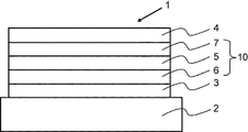
- FIG. 1 is a schematic diagram showing an example of a layer structure of an organic EL element according to an embodiment of the present invention.
- the organic EL device 1 of this example includes a substrate 2, an anode 3, a cathode 4, and a light emitting unit 10 arranged between the anode 3 and the cathode 4.
- the light emitting unit 10 has a light emitting layer 5.
- a hole transport zone 6 hole injection layer, hole transport layer, etc.
- an electron transport zone 7 electron injection layer, electron transport layer
- an electron blocking layer (not shown) may be provided on the anode 3 side of the light emitting layer 5, and a hole blocking layer (not shown) may be provided on the cathode 4 side of the light emitting layer 5.
- FIG. 2 is a schematic diagram showing another example of the layer structure of the organic EL element according to the embodiment of the present invention.
- the organic EL element 11 of this example has a substrate 2, an anode 3, a cathode 4, and a light emitting unit 20 arranged between the anode 3 and the cathode 4.
- the light emitting unit 20 has a light emitting layer 5.
- the hole transport zone arranged between the anode 3 and the light emitting layer 5 is formed of the first hole transport layer 6a and the second hole transport layer 6b.
- the electron transporting zone disposed between the light emitting layer 5 and the cathode 4 is formed by the first electron transporting layer 7a and the second electron transporting layer 7b.
- a single layer electron transport layer and a hole transport layer composed of a plurality of layers may be combined, or a single layer hole transport layer and an electron transport layer composed of a plurality of layers may be combined. Further, the organic EL element 11 may be provided with a hole blocking layer or an electron blocking layer.
- a host combined with a fluorescent dopant is called a fluorescent host
- a host combined with a phosphorescent dopant is called a phosphorescent host
- the fluorescent host and the phosphorescent host are not distinguished from each other only by the molecular structure. That is, the phosphorescent host means a material forming a phosphorescent emitting layer containing a phosphorescent dopant, and does not mean that it cannot be used as a material forming a fluorescent emitting layer. The same applies to the fluorescent host.
- Substrate The substrate is used as a support for the organic EL device.
- a plate made of glass, quartz, plastic, or the like can be used.
- a flexible substrate may be used.
- the flexible substrate include plastic substrates made of polycarbonate, polyarylate, polyether sulfone, polypropylene, polyester, polyvinyl fluoride, polyvinyl chloride, and the like.
- an inorganic vapor deposition film can be used.
- Anode It is preferable to use a metal having a large work function (specifically, 4.0 eV or more), an alloy, an electrically conductive compound, a mixture thereof, or the like for the anode formed on the substrate.
- a metal having a large work function specifically, 4.0 eV or more
- an alloy an electrically conductive compound, a mixture thereof, or the like for the anode formed on the substrate.
- ITO Indium Tin Oxide
- indium oxide-tin oxide containing silicon or silicon oxide indium oxide-zinc oxide
- indium oxide containing tungsten oxide and zinc oxide Examples include graphene and the like.
- gold Au
- platinum Pt
- nickel Ni
- tungsten W
- Cr chromium
- Mo molybdenum
- iron Fe
- Co cobalt
- Cu copper
- palladium Pd
- titanium Ti
- a nitride of the metal for example, titanium nitride
- indium oxide-zinc oxide is a target obtained by adding 1 to 10 wt% zinc oxide to indium oxide, and indium oxide containing tungsten oxide and zinc oxide is 0.5 to 5 wt% tungsten oxide to indium oxide.
- zinc oxide can be formed by a sputtering method by using a target containing 0.1 to 1 wt% of zinc oxide. Alternatively, it may be formed by a vacuum vapor deposition method, a coating method, an inkjet method, a spin coating method, or the like.
- the hole injection layer formed in contact with the anode is formed of a material that facilitates hole injection regardless of the work function of the anode, and thus is generally used as an electrode material (for example, metal).
- an electrode material for example, metal
- alkaline earth metals such as (Sr) and alloys containing these (for example, MgAg, AlLi), rare earth metals such as europium (Eu) and ytterbium (Yb), and alloys containing these.
- a vacuum evaporation method or a sputtering method can be used.
- silver paste or the like a coating method, an inkjet method, or the like can be used.
- the hole injection layer is a layer containing a material having a high hole injection property (hole injection material).
- the hole injecting material may be used alone or in combination of two or more in the hole injecting layer.
- Examples of the hole injecting material include molybdenum oxide, titanium oxide, vanadium oxide, rhenium oxide, ruthenium oxide, chromium oxide, zirconium oxide, hafnium oxide, tantalum oxide, silver oxide, and tungsten oxide. Materials, manganese oxide and the like can be used.
- TDATA 4,4′,4′′-tris(N,N-diphenylamino)triphenylamine
- TDATA 4,4′,4′′-tris(N,N-diphenylamino)triphenylamine
- MTDATA 4,4′,4′′-tris[N-(3- Methylphenyl)-N-phenylamino]triphenylamine
- DPAB 4,4′-bis[N-(4-diphenylaminophenyl)-N-phenylamino]biphenyl
- DNTPD 1,3,5-tris[N -(4-Diphenylaminophenyl)-N-phenylamino]benzene
- DPA3B 1,3,5-tris[N -(4-Diphenylaminophenyl)-N-phenylamino]benzene
- DPA3B 1,3,5-tris[N -(4-Diphenylaminophenyl)-
- High molecular compounds oligomers, dendrimers, polymers, etc.
- PVK poly(N-vinylcarbazole)
- PVTPA poly(4-vinyltriphenylamine)
- PTPDMA poly[N-(4- ⁇ N'-[4-(4-diphenylamino)) Phenyl]phenyl-N'-phenylamino ⁇ phenyl)methacrylamide]
- PTPDMA poly[N,N'-bis(4-butylphenyl)-N,N'-bis(phenyl)benzidine]
- Polymer compounds such as Poly-TPD
- a polymer compound to which an acid such as poly(3,4-ethylenedioxythiophene)/poly(styrenesulfonic acid) (PEDOT/PSS) or polyaniline/poly(styrenesulfonic acid) (PAni/PSS) is added is used. You can also
- acceptor material such as a hexaazatriphenylene (HAT) compound represented by the following formula (K) in combination with another compound.
- HAT hexaazatriphenylene
- R 21 to R 26 are each independently a cyano group, —CONH 2 , a carboxy group, or —COOR 27 (R 27 is an alkyl group having 1 to 20 carbon atoms or 3 to 20 carbon atoms). Represents a cycloalkyl group of R 21 and R 22 , R 23 and R 24 , and two adjacent two selected from R 25 and R 26 are bonded to each other and are represented by —CO—O—CO—.
- R 27 examples include a methyl group, an ethyl group, an n-propyl group, an isopropyl group, an n-butyl group, an isobutyl group, a t-butyl group, a cyclopentyl group and a cyclohexyl group.
- the hole transport layer may contain the above compound (1), and can be used, for example, in combination with the above acceptor material.
- the hole transport layer is a layer containing a material having a high hole transport property (hole transport material).
- the hole transport layer is provided between the anode and the light emitting layer, and when the hole injection layer is present, it is provided between the hole injection layer and the light emitting layer.
- a hole transport material can be used alone or in combination in the hole transport layer.
- the hole transporting material for example, an aromatic amine compound, a carbazole derivative, an anthracene derivative or the like can be used.
- aromatic amine compound examples include 4,4′-bis[N-(1-naphthyl)-N-phenylamino]biphenyl (abbreviation: NPB) and N,N′-bis(3-methylphenyl)-N , N′-diphenyl-[1,1′-biphenyl]-4,4′-diamine (abbreviation: TPD), 4-phenyl-4′-(9-phenylfluoren-9-yl)triphenylamine (abbreviation: BAFLP), 4,4'-bis[N-(9,9-dimethylfluoren-2-yl)-N-phenylamino]biphenyl (abbreviation: DFLDPBi), 4,4',4"-tris(N,N -Diphenylamino)triphenylamine (abbreviation: TDATA), 4,4',4"-tris[N-(3-methylphenyl)-N-phenylamino]
- carbazole derivative examples include 4,4′-di(9-carbazolyl)biphenyl (abbreviation: CBP), 9-[4-(9-carbazolyl)phenyl]-10-phenylanthracene (abbreviation: CzPA), and 9-phenyl-3-[4-(10-phenyl-9-anthryl)phenyl]-9H-carbazole (abbreviation: PCzPA) can be given.
- CBP 4,4′-di(9-carbazolyl)biphenyl
- CzPA 9-[4-(9-carbazolyl)phenyl]-10-phenylanthracene
- PCzPA 9-phenyl-3-[4-(10-phenyl-9-anthryl)phenyl]-9H-carbazole
- anthracene derivative examples include 2-t-butyl-9,10-di(2-naphthyl)anthracene (abbreviation: t-BuDNA), 9,10-di(2-naphthyl)anthracene (abbreviation: DNA), and , 9,10-diphenylanthracene (abbreviation: DPAnth).
- a high molecular compound such as poly(N-vinylcarbazole) (abbreviation: PVK) or poly(4-vinyltriphenylamine) (abbreviation: PVTPA) can also be used.
- PVK poly(N-vinylcarbazole)
- PVTPA poly(4-vinyltriphenylamine)
- compounds other than the above may be used as long as the compounds have a hole transporting property higher than an electron transporting property.
- the hole transport layer may have a single-layer structure or a multi-layer structure including two or more layers.
- the hole transport layer may have a two-layer structure including a first hole transport layer (anode side) and a second hole transport layer (cathode side).
- the compound (1) may be contained in one of the first hole transporting layer and the second hole transporting layer, or may be contained in both.
- the compound (1) is preferably contained in the second hole transport layer, and in another aspect, the compound (1) is contained in the first hole transport layer, and yet another In the aspect, the compound (1) is contained in the first hole transport layer and the second hole transport layer.
- the compound (1) contained in the hole transporting zone or the compound (1) contained in one of the first hole transporting layer and the second hole transporting layer has a low production cost.
- the light hydrogen body (1) is preferable.
- the light hydrogen compound (1) is a compound (1) in which all hydrogen atoms in the formula (1) are light hydrogen atoms. Therefore, in the present invention, the compound (1) contained in the hole transporting zone, or one of the first hole transporting layer and the second hole transporting layer is substantially a deuterium compound (1) only. And an organic EL device containing the compound (1).
- the “compound (1) substantially consisting of the light hydrogen compound (1)” means that the content ratio of the light hydrogen compound (1) to the total amount of the compounds represented by the formula (1) is 90 mol% or more, preferably Means 95 mol% or more, more preferably 99 mol% or more (including 100% of each).
- the light-emitting layer is a layer containing a material having a high light-emitting property (dopant material), and various materials can be used.
- a fluorescent light emitting material or a phosphorescent light emitting material can be used as a dopant material.
- a fluorescent material is a compound that emits light from a singlet excited state
- a phosphorescent material is a compound that emits light from a triplet excited state.
- a pyrene derivative, a styrylamine derivative, a chrysene derivative, a fluoranthene derivative, a fluorene derivative, a diamine derivative, a triarylamine derivative, or the like can be used as a blue-based fluorescent light emitting material that can be used in the light emitting layer.
- N,N′-bis[4-(9H-carbazol-9-yl)phenyl]-N,N′-diphenylstilbene-4,4′-diamine (abbreviation: YGA2S), 4-(9H -Carbazol-9-yl)-4'-(10-phenyl-9-anthryl)triphenylamine (abbreviation: YGAPA), 4-(10-phenyl-9-anthryl)-4'-(9-phenyl-9H -Carbazol-3-yl)triphenylamine (abbreviation: PCBAPA) and the like.
- An aromatic amine derivative or the like can be used as a green fluorescent material that can be used for the light emitting layer.
- 2PCAPA N-(9,10-diphenyl-2-anthryl)-N,9-diphenyl-9H-carbazol-3-amine
- 2PCABPhA N-[9,10-bis(1,1) '-Biphenyl-2-yl)-2-anthryl]-N,9-diphenyl-9H-carbazol-3-amine
- 2DPAPA N-(9,10-diphenyl-2-anthryl)-N,N ',N'-Triphenyl-1,4-phenylenediamine
- 2DPAPA N-[9,10-bis(1,1'-biphenyl-2-yl)-2-anthryl]-N,N' , N'-triphenyl-1,4-phenylenediamine
- 2DPABPhA N-[9,10-bis(1,1'-biphenyl
- a tetracene derivative, a diamine derivative, or the like can be used as a red fluorescent light emitting material that can be used in the light emitting layer.
- N,N,N′,N′-tetrakis(4-methylphenyl)tetracene-5,11-diamine abbreviation: p-mPhTD
- 7,14-diphenyl-N,N,N′ examples thereof include N'-tetrakis(4-methylphenyl)acenaphtho[1,2-a]fluoranthene-3,10-diamine (abbreviation: p-mPhAFD).
- a metal complex such as an iridium complex, an osmium complex or a platinum complex is used as a blue phosphorescent light emitting material that can be used in the light emitting layer.
- a metal complex such as an iridium complex, an osmium complex or a platinum complex
- FIr6 bis[2-(4′,6′-difluorophenyl)pyridinato-N,C2′]iridium(III) tetrakis(1-pyrazolyl)borate
- FIrpic bis[2-(4′ ,6′-Difluorophenyl)pyridinato-N,C2′]iridium(III) picolinate
- FIrpic bis[2-(3′,5′bistrifluoromethylphenyl)pyridinato-N,C2′]iridium(III) ) Picolinate
- Ir(CF3ppy)2(pic) bis[2-(4′,6′-d
- An iridium complex or the like is used as a green phosphorescent material that can be used in the light emitting layer.
- Tris(2-phenylpyridinato-N,C2′)iridium(III) (abbreviation: Ir(ppy)3), bis(2-phenylpyridinato-N,C2′)iridium(III)acetylacetonate( Abbreviation: Ir(ppy)2(acac)), bis(1,2-diphenyl-1H-benzimidazolato)iridium(III) acetylacetonate (abbreviation: Ir(pbi)2(acac)), bis(benzo[ h]quinolinato)iridium(III) acetylacetonate (abbreviation: Ir(bzq)2(acac)) and the like.
- a metal complex such as an iridium complex, a platinum complex, a terbium complex or a europium complex is used as a red phosphorescent light emitting material that can be used in the light emitting layer.
- a metal complex such as an iridium complex, a platinum complex, a terbium complex or a europium complex
- Ir(btp)2(acac) bis[2-(2′-benzo[4,5- ⁇ ]thienyl)pyridinato-N,C3′]iridium(III)acetylacetonate
- Ir(btp)2(acac) bis(1-phenylisoquinolinato-N,C2′)iridium(III)acetylacetonate
- Ir(piq)2(acac) bis(1-phenylisoquinolinato-N,C2′)iridium(III)acetylacetonate
- tris(acetylacetonato)(monophenanthroline)terbium(III) (abbreviation: Tb(acac)3(Phen)
- tris(1,3-diphenyl-1,3-propanedionate)(monophenanthroline) europium (III) (abbreviation: Eu(DBM)3(Phen)
- tris[1-(2-thenoyl)-3,3,3-trifluoroacetonato](monophenanthroline) europium(III) (abbreviation: Eu( A rare earth metal complex such as TTA)3(Phen)) emits light from a rare earth metal ion (electron transition between different multiplicities) and thus can be used as a phosphorescent material.
- the light-emitting layer may have a structure in which the above-mentioned dopant material is dispersed in another material (host material).
- the host material it is preferable to use a material having a lowest unoccupied molecular orbital level (LUMO level) and a highest occupied molecular orbital level (HOMO level) lower than those of the dopant material.
- LUMO level lowest unoccupied molecular orbital level
- HOMO level highest occupied molecular orbital level
- a metal complex such as an aluminum complex, a beryllium complex, or a zinc complex
- a heterocyclic compound such as an oxadiazole derivative, a benzimidazole derivative, or a phenanthroline derivative
- a condensed aromatic compound such as a carbazole derivative, anthracene derivative, phenanthrene derivative, pyrene derivative, or chrysene derivative
- An aromatic amine compound such as a triarylamine derivative or a condensed polycyclic aromatic amine derivative is used.
- tris(8-quinolinolato)aluminum(III) (abbreviation: Alq)
- tris(4-methyl-8-quinolinolato)aluminum(III) (abbreviation: Almq3)
- bis(10-hydroxybenzo[h]quinolinato)beryllium (II) (abbreviation: BeBq2)
- bis(2-methyl-8-quinolinolato)(4-phenylphenolato)aluminum(III) abbreviation: BAlq
- bis(8-quinolinolato)zinc(II) (abbreviation: Znq)
- bis[2-(2-benzoxazolyl)phenolato]zinc(II) (abbreviation: ZnPBO)
- bis[2-(2-benzothiazolyl)phenolato]zinc(II) (abbreviation: ZnBTZ), and other metal complexes.
- anthracene compound in the case of a blue fluorescent element, it is preferable to use the following anthracene compound as a host material.
- the electron transport zone is composed of an electron injection layer, an electron transport layer, a hole blocking layer, etc.
- any layer in the electron transporting zone, particularly the electron transporting layer is preferably an alkali metal, an alkaline earth metal, a rare earth metal, an oxide of an alkali metal, a halide of an alkali metal, an oxide of an alkaline earth metal.
- the electron transport layer is a layer containing a material having a high electron transport property (electron transport material).
- the electron transport layer is provided between the cathode and the light emitting layer, and when the electron injection layer is present, it is provided between the electron injection layer and the light emitting layer.
- the electron transport layer for example, (1) Metal complexes such as aluminum complex, beryllium complex and zinc complex, (2) Heteroaromatic compounds such as imidazole derivative, benzimidazole derivative, azine derivative, carbazole derivative and phenanthroline derivative, (3) A polymer compound can be used.
- metal complex examples include tris(8-quinolinolato)aluminum(III) (abbreviation: Alq), tris(4-methyl-8-quinolinolato)aluminum (abbreviation: Almq3), bis(10-hydroxybenzo[h]quinolinato.
- Beryllium (abbreviation: BeBq 2 ), bis(2-methyl-8-quinolinolato)(4-phenylphenolato)aluminum(III) (abbreviation: BAlq), bis(8-quinolinolato)zinc(II) (abbreviation: Znq) ), bis[2-(2-benzoxazolyl)phenolato]zinc(II) (abbreviation: ZnPBO), and bis[2-(2-benzothiazolyl)phenolato]zinc(II) (abbreviation: ZnBTZ).
- BeBq 2 Beryllium (abbreviation: BeBq 2 ), bis(2-methyl-8-quinolinolato)(4-phenylphenolato)aluminum(III) (abbreviation: BAlq), bis(8-quinolinolato)zinc(II) (abbreviation: Znq) ), bis[2-(2-benzoxazolyl
- heteroaromatic compound examples include 2-(4-biphenylyl)-5-(4-tert-butylphenyl)-1,3,4-oxadiazole (abbreviation: PBD) and 1,3-bis[5 -(Ptert-butylphenyl)-1,3,4-oxadiazol-2-yl]benzene (abbreviation: OXD-7), 3-(4-tert-butylphenyl)-4-phenyl-5-(4 -Biphenylyl)-1,2,4-triazole (abbreviation: TAZ), 3-(4-tert-butylphenyl)-4-(4-ethylphenyl)-5-(4-biphenylyl)-1,2,4 -Triazole (abbreviation: p-EtTAZ), bathophenanthroline (abbreviation: BPhen), bathocuproine (abbreviation: BCP), 4,4'-bis(5-methylbenzo
- polymer compound examples include poly[(9,9-dihexylfluorene-2,7-diyl)-co-(pyridine-3,5-diyl)] (abbreviation: PF-Py), poly[(9, 9-dioctylfluorene-2,7-diyl)-co-(2,2′-bipyridine-6,6′-diyl)] (abbreviation: PF-BPy).
- the above material is a material having an electron mobility of 10 ⁇ 6 cm 2 /Vs or more. Note that a material other than the above may be used for the electron-transporting layer as long as the material has a higher electron-transporting property than a hole-transporting property.
- the electron transport layer may be a single layer or a multilayer including two or more layers.
- the electron transport layer may be a layer including a first electron transport layer (anode side) and a second electron transport layer (cathode side).
- the two or more electron transport layers are each formed of the electron transport material.
- the electron injection layer is a layer containing a material having a high electron injection property.
- the electron injection layer includes lithium (Li), cesium (Cs), calcium (Ca), lithium fluoride (LiF), cesium fluoride (CsF), calcium fluoride (CaF2), lithium oxide (LiOx), and the like.
- Alkali metals, alkaline earth metals, or compounds thereof can be used.
- a material having an electron-transporting property containing an alkali metal, an alkaline earth metal, or a compound thereof, specifically, a material containing Alq containing magnesium (Mg) or the like may be used. In this case, electron injection from the cathode can be performed more efficiently.
- a composite material obtained by mixing an organic compound and an electron donor (donor) may be used for the electron injection layer.
- a composite material has an excellent electron injecting property and an electron transporting property because the organic compound receives an electron from the electron donor.
- the organic compound is preferably a material excellent in transporting received electrons, and specifically, for example, the above-mentioned material constituting the electron transport layer (metal complex, heteroaromatic compound, etc.) is used. be able to.
- the electron donor any material having an electron donating property with respect to the organic compound may be used.
- alkali metals, alkaline earth metals and rare earth metals are preferable, and examples thereof include lithium, cesium, magnesium, calcium, erbium and ytterbium.
- alkali metal oxides and alkaline earth metal oxides are preferable, and lithium oxide, calcium oxide, barium oxide and the like can be mentioned.
- a Lewis base such as magnesium oxide.
- an organic compound such as tetrathiafulvalene (abbreviation: TTF) can be used.
- Cathode For the cathode, it is preferable to use a metal, an alloy, an electrically conductive compound, a mixture thereof, or the like having a low work function (specifically, 3.8 eV or less).
- a cathode material include elements belonging to Group 1 or Group 2 of the periodic table of the elements, that is, alkali metals such as lithium (Li) and cesium (Cs), and magnesium (Mg) and calcium (Ca). ), strontium (Sr) and other alkaline earth metals, and alloys containing these (eg MgAg, AlLi), europium (Eu), ytterbium (Yb) and other rare earth metals and alloys containing these.
- a vacuum evaporation method or a sputtering method can be used.
- a coating method, an inkjet method, or the like can be used.
- a cathode is formed using various conductive materials such as Al, Ag, ITO, graphene, indium oxide-tin oxide containing silicon or silicon oxide, regardless of the work function. can do.
- These conductive materials can be formed by a sputtering method, an inkjet method, a spin coating method, or the like.
- Insulating layer The organic EL element is likely to cause pixel defects due to leakage or short circuit because an electric field is applied to the ultrathin film.
- an insulating layer formed of an insulating thin film layer may be inserted between the pair of electrodes.
- the material used for the insulating layer include aluminum oxide, lithium fluoride, lithium oxide, cesium fluoride, cesium oxide, magnesium oxide, magnesium fluoride, calcium oxide, calcium fluoride, aluminum nitride, titanium oxide, silicon oxide. , Germanium oxide, silicon nitride, boron nitride, molybdenum oxide, ruthenium oxide, vanadium oxide and the like. In addition, you may use these mixtures and laminated bodies.
- the space layer for example, when laminating a fluorescent light emitting layer and a phosphorescent light emitting layer, do not diffuse excitons generated in the phosphorescent light emitting layer into the fluorescent light emitting layer, or for the purpose of adjusting the carrier balance, It is a layer provided between the fluorescent light emitting layer and the phosphorescent light emitting layer. Further, the space layer may be provided between the plurality of phosphorescent emitting layers.
- carrier as used herein means a charge carrier in a substance. Since the space layer is provided between the light emitting layers, it is preferably a material having both electron transporting property and hole transporting property. Further, the triplet energy is preferably 2.6 eV or more in order to prevent the diffusion of triplet energy in the adjacent phosphorescent emitting layer. Examples of the material used for the space layer include the same materials as those used for the hole transport layer described above.
- a blocking layer such as an electron blocking layer, a hole blocking layer or an exciton blocking layer may be provided adjacent to the light emitting layer.
- the electron blocking layer is a layer that prevents electrons from leaking from the light emitting layer to the hole transporting layer.
- the hole transport layer closest to the light emitting layer may function as the electron blocking layer.
- the hole blocking layer is a layer that prevents holes from leaking from the light emitting layer to the electron transporting layer.
- the electron transport layer closest to the light emitting layer may function as the hole blocking layer.
- the exciton blocking layer has a function of preventing excitons generated in the light emitting layer from diffusing into a peripheral layer and confining the excitons in the light emitting layer.
- Each layer of the organic EL element can be formed by a conventionally known vapor deposition method, coating method, or the like.
- a vapor deposition method such as a vacuum vapor deposition method or a molecular beam vapor deposition method (MBE method), or a dipping method, a spin coating method, a casting method, a bar coating method, a roll coating method or the like using a solution of a compound forming a layer. It can be formed by a known method according to the above coating method.
- the film thickness of each layer is not particularly limited, but generally, if the film thickness is too thin, defects such as pinholes are likely to occur, and conversely, if it is too thick, a high driving voltage is required and efficiency deteriorates, so it is usually 5 nm to 10 ⁇ m. 10 nm to 0.2 ⁇ m is more preferable.
- the organic EL element can be used for display parts such as organic EL panel modules, display devices such as televisions, mobile phones and personal computers, and electronic devices such as lighting and light emitting devices for vehicle lighting.
- Example 1 A 25 mm ⁇ 75 mm ⁇ 1.1 mm thick glass substrate with an ITO transparent electrode (manufactured by Geomatec Co., Ltd.) was subjected to ultrasonic cleaning in isopropyl alcohol for 5 minutes, and then UV ozone cleaning for 30 minutes. The thickness of the ITO transparent electrode was 130 nm.
- the glass substrate with the ITO transparent electrode line after washing was mounted on the substrate holder of the vacuum vapor deposition apparatus, and the compound HT-1 was prepared by covering the transparent electrode on the surface on which the ITO transparent electrode line was formed. And the above compound HI-1 were co-evaporated to form a co-evaporated film having a film thickness of 10 nm to form a hole injection layer.
- the concentration of HI-1 in the hole injection layer was 3% by mass.
- the above compound HT-1 was vapor-deposited as a material for the first hole transport layer on the hole injection layer to form a first hole transport layer having a film thickness of 75 nm.
- the compound 1 synthesized in Synthesis Example 1 below was deposited as a second hole transport layer material to form a second hole transport layer having a film thickness of 15 nm.
- the compound BH-1 (host material) and the compound BD-1 (dopant material) were co-evaporated on the second hole transport layer to form a co-evaporated film having a thickness of 25 nm.
- the concentration of compound BD-1 in this co-deposited film was 4% by mass.
- This co-deposited film functions as a light emitting layer.
- the compound ET-1 was vapor-deposited on the light emitting layer to form a film having a thickness of 5 nm to form a first electron transporting layer.
- the compound ET-2 and the compound ET-3 were co-evaporated on the first electron transport layer to form a co-deposited film having a film thickness of 25 nm to form a second electron transport layer.
- the concentration of the compound ET-3 in the second electron transport layer was 33% by mass.
- LiF was vapor-deposited on the second electron transport layer to form a LiF film having a film thickness of 1 nm to form an electron injecting electrode (cathode).
- Example 1 The device configuration of Example 1 is schematically shown as follows. ITO(130)/HT-1:HI-1(10:3%)/HT-1(75)/Compound 1(15)/BH-1:BD-1(25:4%)/ET-1( 5)/ET-2:ET-3(25:33%)/LiF(1)/Al(50)
- the number in parentheses indicates the film thickness (unit: nm). Similarly, in parentheses, the number expressed as a percentage indicates the proportion (% by mass) of the compound described on the right side in that layer. The same applies to the corresponding descriptions in the following examples and comparative examples.
- Examples 2 to 6 instead of the compound 1 used in the second hole transport layer of Example 1, compounds 2 to 6 synthesized in the following synthesis examples 2 to 6 were used as the hole transport material of the second hole transport layer. An organic EL element was manufactured in the same manner as in Example 1 to obtain the organic EL elements of Examples 2 to 6.
- Comparative Examples 1 to 6 In the same manner as in Example 1 except that the above-mentioned Comparative Compounds 1 to 6 were used as the hole transporting materials of the second hole transporting layer instead of the compound 1 used in the second hole transporting layer of Example 1. Organic EL devices were produced by using the organic EL devices of Comparative Examples 1 to 6.
- Example 7 A 25 mm ⁇ 75 mm ⁇ 1.1 mm thick glass substrate with an ITO transparent electrode (manufactured by Geomatec Co., Ltd.) was subjected to ultrasonic cleaning in isopropyl alcohol for 5 minutes, and then UV ozone cleaning for 30 minutes. The thickness of the ITO transparent electrode was 130 nm.
- the glass substrate with the ITO transparent electrode line after washing was mounted on the substrate holder of the vacuum vapor deposition apparatus, and the transparent electrode was first covered on the surface on the side where the ITO transparent electrode line was formed to synthesize in Synthesis Example 1.
- the hole injection layer was formed by co-evaporating the compound 1 and the compound HI-1 described above to form a co-evaporation film having a film thickness of 10 nm.
- the concentration of HI-1 in the hole injection layer was 15% by mass.
- the compound 1 synthesized in Synthesis Example 1 was vapor-deposited as a material for the first hole transport layer to form a first hole transport layer having a film thickness of 80 nm.
- the compound HT-2 was vapor-deposited as a second hole transport layer material on the first hole transport layer to form a second hole transport layer having a film thickness of 10 nm.
- the compound BH-1 (host material) and the compound BD-1 (dopant material) were co-evaporated on the second hole transport layer to form a co-evaporated film having a thickness of 25 nm.
- the concentration of compound BD-1 in this co-deposited film was 4% by mass.
- This co-deposited film functions as a light emitting layer.
- the compound ET-4 and the compound ET-5 were co-deposited on the light emitting layer to form a co-deposited film having a film thickness of 20 nm, thereby forming an electron transport layer.
- the concentration of compound ET-5 in the electron transport layer was 50% by mass.
- LiF was vapor-deposited on the electron transport layer to form a LiF film having a film thickness of 1 nm to form an electron injecting electrode (cathode).
- metal Al was vapor-deposited on this LiF film to form a metal Al film having a film thickness of 50 nm, and a metal Al cathode was formed to obtain an organic EL device of Example 7.
- the device configuration of Example 7 is schematically shown as follows. ITO(130)/Compound 1:HI-1(10:15%)/Compound 1(80)/HT-2(10)/BH-1:BD-1(25:4%)/ET-4:ET -5(20:50%)/LiF(1)/Al(
- Example 8 to 12 instead of the compound 1 used in the hole injection layer and the first hole transport layer of Example 7, the compounds 2 to 6 synthesized in the above Synthesis Examples 2 to 6 were used to form the hole injection layer and the first hole, respectively.
- Organic EL devices were produced in the same manner as in Example 7 except that they were used as the hole transporting material for the transport layer, to obtain organic EL devices of Examples 8-12.
- Comparative Examples 7 to 12 instead of the compound 1 used for the hole injection layer and the first hole transport layer of Example 7, the above-mentioned comparative compounds 1 to 6 were used, respectively, for the hole transport material of the hole injection layer and the first hole transport layer.
- Organic EL devices were prepared in the same manner as in Example 7 except that the organic EL devices of Comparative Examples 7 to 12 were used.
- ⁇ Evaluation 1 of organic EL device> With respect to the organic EL devices manufactured in Examples 1 to 12 and Comparative Examples 1 to 12, a voltage was applied to the organic EL devices so that the current density was 10 mA/cm 2, and the external quantum efficiency was evaluated.
- ⁇ Evaluation 2 of organic EL element> With respect to the organic EL elements of Examples 1 to 12 and Comparative Examples 1 to 12, a voltage was applied to the organic EL elements so that the current density was 50 mA/cm 2, and the 95% life (LT95) was evaluated.
- LT95 refers to the time (hr) until the luminance decreases to 95% of the initial luminance during constant current driving.
- the results of Evaluation 1 and Evaluation 2 are shown in Tables 1 and 2.
- Comparative Compounds 1 to 6 were used by using Compounds 1 to 6 having a specific structure and included in Formula (1) as the hole transport material of the organic EL device. It can be seen that it is possible to obtain an organic EL element that can achieve both longevity and high efficiency, which cannot be realized by the organic EL element.
- the reason why the organic EL device using the compounds 1 to 6 has higher performances in both lifetime and external quantum efficiency than the organic EL devices using the comparative compounds 1 to 6 is not limited to this. It is presumed that this is because the compound defined in the present application is a compound that is very stable with respect to electrons and excitons while enhancing the barrier ability of confining excitons in the light emitting layer.
- the organic EL devices of Comparative Examples 1 to 12 have lower external quantum efficiency and/or life than those of Examples 1 to 12. It is considered that this is because at least one of the barrier ability and the stability is impaired because the molecular structures of Comparative Compounds 1 to 6 deviate from the structure defined by Compound (1).
- the mixture was returned to room temperature, water was added, extraction was performed with toluene, the obtained toluene layer was dried over anhydrous sodium sulfate, and concentrated under reduced pressure.
- the obtained residue was purified by silica gel column chromatography to obtain 3.07 g of a white solid. The yield was 65%.
- the reaction solution was cooled to room temperature, filtered through Celite, and the filtrate was concentrated under reduced pressure.
- the obtained residue was purified by silica gel column chromatography and recrystallization to obtain 20.6 g of white solid.
- the yield was 62%.
- the reaction solution was cooled to room temperature, and the filtrate was concentrated under reduced pressure.
- the obtained residue was purified by silica gel column chromatography and recrystallization to obtain 46 g of a white solid.
- the yield was 73%.
- the obtained residue was purified by silica gel column chromatography and recrystallization to obtain 4.28 g of a white solid.
- the yield was 65%.
Landscapes
- Chemical & Material Sciences (AREA)
- Organic Chemistry (AREA)
- Physics & Mathematics (AREA)
- Spectroscopy & Molecular Physics (AREA)
- Engineering & Computer Science (AREA)
- Materials Engineering (AREA)
- Optics & Photonics (AREA)
- Electroluminescent Light Sources (AREA)
- Organic Low-Molecular-Weight Compounds And Preparation Thereof (AREA)
- Furan Compounds (AREA)
- Plural Heterocyclic Compounds (AREA)
Priority Applications (6)
| Application Number | Priority Date | Filing Date | Title |
|---|---|---|---|
| EP19888913.1A EP3889151A4 (en) | 2018-11-30 | 2019-11-29 | COMPOUND, ORGANIC ELECTROLUMINESCENT ELEMENT MATERIAL, ORGANIC ELECTROLUMINESCENT ELEMENT AND ELECTRONIC DEVICE |
| JP2020557867A JP7461300B2 (ja) | 2018-11-30 | 2019-11-29 | 化合物、有機エレクトロルミネッセンス素子用材料、有機エレクトロルミネッセンス素子、及び、電子機器 |
| CN201980078775.1A CN113227083A (zh) | 2018-11-30 | 2019-11-29 | 化合物、有机电致发光元件用材料、有机电致发光元件和电子设备 |
| KR1020217015601A KR102705700B1 (ko) | 2018-11-30 | 2019-11-29 | 화합물, 유기 전기발광 소자용 재료, 유기 전기발광 소자, 및 전자 기기 |
| US16/881,656 US11548877B2 (en) | 2018-11-30 | 2020-05-22 | Compound, material for organic electroluminescence device, organic electroluminescence device, and electronic device |
| US17/861,301 US12338234B2 (en) | 2018-11-30 | 2022-07-11 | Compound, material for organic electroluminescence device, organic electroluminescence device, and electronic device |
Applications Claiming Priority (4)
| Application Number | Priority Date | Filing Date | Title |
|---|---|---|---|
| JP2018225423 | 2018-11-30 | ||
| JP2018-225423 | 2018-11-30 | ||
| JP2019-069354 | 2019-03-29 | ||
| JP2019069354 | 2019-03-29 |
Related Child Applications (1)
| Application Number | Title | Priority Date | Filing Date |
|---|---|---|---|
| US16/881,656 Continuation US11548877B2 (en) | 2018-11-30 | 2020-05-22 | Compound, material for organic electroluminescence device, organic electroluminescence device, and electronic device |
Publications (1)
| Publication Number | Publication Date |
|---|---|
| WO2020111251A1 true WO2020111251A1 (ja) | 2020-06-04 |
Family
ID=70852819
Family Applications (2)
| Application Number | Title | Priority Date | Filing Date |
|---|---|---|---|
| PCT/JP2019/046861 Ceased WO2020111251A1 (ja) | 2018-11-30 | 2019-11-29 | 化合物、有機エレクトロルミネッセンス素子用材料、有機エレクトロルミネッセンス素子、及び、電子機器 |
| PCT/JP2019/046863 Ceased WO2020111253A1 (ja) | 2018-11-30 | 2019-11-29 | 化合物、有機エレクトロルミネッセンス素子用材料、有機エレクトロルミネッセンス素子、及び、電子機器 |
Family Applications After (1)
| Application Number | Title | Priority Date | Filing Date |
|---|---|---|---|
| PCT/JP2019/046863 Ceased WO2020111253A1 (ja) | 2018-11-30 | 2019-11-29 | 化合物、有機エレクトロルミネッセンス素子用材料、有機エレクトロルミネッセンス素子、及び、電子機器 |
Country Status (6)
| Country | Link |
|---|---|
| US (2) | US11548877B2 (https=) |
| EP (1) | EP3889151A4 (https=) |
| JP (1) | JP7461300B2 (https=) |
| KR (1) | KR102705700B1 (https=) |
| CN (1) | CN113227083A (https=) |
| WO (2) | WO2020111251A1 (https=) |
Cited By (5)
| Publication number | Priority date | Publication date | Assignee | Title |
|---|---|---|---|---|
| EP4012795A1 (en) * | 2020-12-09 | 2022-06-15 | Samsung Display Co., Ltd. | Luminescence device and amine compound for organic electroluminescence device |
| WO2022230963A1 (ja) * | 2021-04-28 | 2022-11-03 | 出光興産株式会社 | 化合物、有機エレクトロルミネッセンス素子用材料、有機エレクトロルミネッセンス素子及び電子機器 |
| US11548877B2 (en) | 2018-11-30 | 2023-01-10 | Idemitsu Kosan Co., Ltd. | Compound, material for organic electroluminescence device, organic electroluminescence device, and electronic device |
| US20230027888A1 (en) * | 2021-06-25 | 2023-01-26 | Idemitsu Kosan Co.,Ltd. | Organic electroluminescent device, organic electroluminescence display device, electronic device and compound |
| KR20230145363A (ko) | 2021-02-26 | 2023-10-17 | 이데미쓰 고산 가부시키가이샤 | 화합물, 유기 전기발광 소자용 재료, 유기 전기발광소자 및 전자 기기 |
Families Citing this family (10)
| Publication number | Priority date | Publication date | Assignee | Title |
|---|---|---|---|---|
| US11479544B2 (en) * | 2017-03-08 | 2022-10-25 | Idemitsu Kosan Co., Ltd. | Compound, material for organic electroluminescence element, organic electroluminescence element, and electronic device |
| EP3939970B1 (en) | 2019-03-15 | 2023-12-27 | Idemitsu Kosan Co., Ltd. | Compound, material for organic electroluminescence devices, organic electroluminescence device, and electronic device |
| US12048242B2 (en) | 2019-05-31 | 2024-07-23 | Idemitsu Kosan Co., Ltd. | Compound, material for organic electroluminescent elements, organic electroluminescent element, and electronic device |
| WO2021162227A1 (ko) * | 2020-02-13 | 2021-08-19 | 주식회사 엘지화학 | 신규한 화합물 및 이를 이용한 유기 발광 소자 |
| KR102697568B1 (ko) * | 2020-10-16 | 2024-08-23 | 주식회사 엘지화학 | 화합물 및 이를 포함하는 유기 발광 소자 |
| KR20220086754A (ko) * | 2020-12-16 | 2022-06-24 | 삼성디스플레이 주식회사 | 유기 전계 발광 소자 및 유기 전계 발광 소자용 아민 화합물 |
| US20230371368A1 (en) * | 2022-05-11 | 2023-11-16 | Samsung Display Co., Ltd. | Light emitting element and amine compound for the same |
| CN117263812A (zh) * | 2023-09-20 | 2023-12-22 | 京东方科技集团股份有限公司 | 一种用于有机电致发光器件中的芳香胺化合物及其制备方法和应用 |
| KR102943276B1 (ko) | 2023-09-22 | 2026-03-24 | 덕산네오룩스 주식회사 | 유기전기소자용 화합물을 포함하는 유기전기소자 및 그 전자 장치 |
| KR20250142797A (ko) | 2024-03-22 | 2025-09-30 | 머티어리얼사이언스 주식회사 | 유기 화합물 및 이를 포함하는 유기발광소자 |
Citations (19)
| Publication number | Priority date | Publication date | Assignee | Title |
|---|---|---|---|---|
| WO2007125714A1 (ja) | 2006-04-26 | 2007-11-08 | Idemitsu Kosan Co., Ltd. | 芳香族アミン誘導体及びそれらを用いた有機エレクトロルミネッセンス素子 |
| WO2010061824A1 (ja) | 2008-11-25 | 2010-06-03 | 出光興産株式会社 | 芳香族アミン誘導体及び有機エレクトロルミネッセンス素子 |
| WO2011059099A1 (ja) * | 2009-11-16 | 2011-05-19 | 出光興産株式会社 | 芳香族アミン誘導体及びそれを用いた有機エレクトロルミネッセンス素子 |
| WO2012091471A2 (ko) | 2010-12-28 | 2012-07-05 | 덕산하이메탈(주) | 화합물 및 이를 이용한 유기전기소자, 그 전자장치 |
| WO2016006711A1 (ja) | 2014-07-11 | 2016-01-14 | 出光興産株式会社 | 化合物、有機エレクトロルミネッセンス素子用材料、有機エレクトロルミネッセンス素子、及び電子機器 |
| JP2016066723A (ja) | 2014-09-25 | 2016-04-28 | 三星ディスプレイ株式會社Samsung Display Co.,Ltd. | 有機電界発光素子用材料及びこれを用いた有機電界発光素子 |
| JP2016086142A (ja) | 2014-10-29 | 2016-05-19 | 三星ディスプレイ株式會社Samsung Display Co.,Ltd. | 有機エレクトロルミネッセンス素子用材料及びそれを用いた有機エレクトロルミネッセンス素子 |
| WO2016199784A1 (ja) | 2015-06-08 | 2016-12-15 | 出光興産株式会社 | 化合物、有機エレクトロルミネッセンス素子用材料、有機エレクトロルミネッセンス素子、及び電子機器 |
| JP2016219797A (ja) * | 2015-05-19 | 2016-12-22 | パナソニック株式会社 | 光発電素子 |
| WO2017012687A1 (en) | 2015-07-22 | 2017-01-26 | Merck Patent Gmbh | Materials for organic electroluminescent devices |
| JP2017522713A (ja) * | 2014-03-27 | 2017-08-10 | メルク パテント ゲーエムベーハー | 発光装置および電子機器 |
| KR20170094665A (ko) | 2016-02-11 | 2017-08-21 | 주식회사 엘지화학 | 화합물 및 이를 이용한 유기 전계 발광 소자 |
| WO2017148564A1 (de) | 2016-03-03 | 2017-09-08 | Merck Patent Gmbh | Materialien für organische elektrolumineszenzvorrichtungen |
| JP2017183727A (ja) * | 2016-03-30 | 2017-10-05 | 三星ディスプレイ株式會社Samsung Display Co.,Ltd. | 有機電界発光素子 |
| KR20180061077A (ko) * | 2016-11-29 | 2018-06-07 | 주식회사 엘지화학 | 신규한 화합물 및 이를 이용한 유기발광 소자 |
| WO2018164239A1 (ja) | 2017-03-08 | 2018-09-13 | 出光興産株式会社 | 化合物、有機エレクトロルミネッセンス素子用材料、有機エレクトロルミネッセンス素子、及び電子機器 |
| KR20180112962A (ko) * | 2017-04-05 | 2018-10-15 | (주)피엔에이치테크 | 유기발광 화합물 및 이를 포함하는 유기전계발광소자 |
| KR20190079181A (ko) * | 2017-12-27 | 2019-07-05 | 주식회사 두산 | 유기 화합물 및 이를 포함하는 유기 전계 발광 소자 |
| WO2019146781A1 (ja) | 2018-01-29 | 2019-08-01 | 出光興産株式会社 | 化合物及びそれを用いた有機エレクトロルミネッセンス素子 |
Family Cites Families (77)
| Publication number | Priority date | Publication date | Assignee | Title |
|---|---|---|---|---|
| KR102128702B1 (ko) * | 2012-08-21 | 2020-07-02 | 롬엔드하스전자재료코리아유한회사 | 신규한 유기 전계 발광 화합물 및 이를 포함하는 유기 전계 발광 소자 |
| KR102136040B1 (ko) | 2013-03-26 | 2020-07-20 | 가부시키가이샤 한도오따이 에네루기 켄큐쇼 | 유기 화합물, 발광 소자, 발광 장치, 표시 장치, 전자 기기 및 조명 장치 |
| US10236464B2 (en) | 2014-08-21 | 2019-03-19 | Samsung Display Co., Ltd. | Organic light emitting diode |
| US11211575B2 (en) | 2014-08-21 | 2021-12-28 | Samsung Display Co., Ltd. | Organic light emitting diode |
| KR20160027940A (ko) | 2014-09-02 | 2016-03-10 | 주식회사 엘지화학 | 유기 발광 소자 |
| KR102311695B1 (ko) * | 2014-11-06 | 2021-10-12 | 덕산네오룩스 주식회사 | 유기전기소자용 조성물을 이용한 디스플레이 장치 및 유기전기소자 |
| KR102292572B1 (ko) * | 2014-11-07 | 2021-08-24 | 덕산네오룩스 주식회사 | 유기전기소자용 조성물을 이용한 디스플레이 장치 및 유기전기소자 |
| KR102277378B1 (ko) | 2015-01-19 | 2021-07-14 | 삼성디스플레이 주식회사 | 유기 발광 소자 및 이를 포함하는 유기 발광 표시 장치 |
| TWI749726B (zh) | 2015-03-09 | 2021-12-11 | 日商半導體能源研究所股份有限公司 | 發光元件、顯示裝置、電子裝置及照明設備 |
| KR102459818B1 (ko) | 2015-05-06 | 2022-10-27 | 삼성디스플레이 주식회사 | 유기 발광 표시 장치 |
| WO2016178544A2 (ko) * | 2015-05-06 | 2016-11-10 | 주식회사 동진쎄미켐 | 신규한 화합물 및 이를 포함하는 유기발광소자 |
| JP6661289B2 (ja) * | 2015-07-08 | 2020-03-11 | 三星ディスプレイ株式會社Samsung Display Co.,Ltd. | 有機エレクトロルミネッセンス素子用材料及びそれを用いた有機エレクトロルミネッセンス素子 |
| US20170025609A1 (en) | 2015-07-20 | 2017-01-26 | E I Du Pont De Nemours And Company | Electroactive materials |
| US11018304B2 (en) | 2015-11-30 | 2021-05-25 | Samsung Display Co., Ltd. | Organic light-emitting device |
| KR101959512B1 (ko) * | 2016-10-14 | 2019-03-18 | 주식회사 엘지화학 | 신규한 화합물 및 이를 포함하는 유기발광 소자 |
| EP3312166B1 (en) * | 2016-10-21 | 2019-11-27 | Samsung Display Co., Ltd. | Monoamine compound and organic electroluminescence device including the same |
| CN108401295B (zh) | 2017-02-05 | 2020-06-30 | 维沃移动通信有限公司 | 一种波束恢复处理方法、网络侧设备及移动终端 |
| JP2020097525A (ja) | 2017-03-10 | 2020-06-25 | 出光興産株式会社 | 化合物、有機エレクトロルミネッセンス素子用材料、有機エレクトロルミネッセンス素子、及び電子機器 |
| TW201843143A (zh) | 2017-03-13 | 2018-12-16 | 德商麥克專利有限公司 | 含有芳基胺結構之化合物 |
| US20200091435A1 (en) | 2017-03-24 | 2020-03-19 | Idemitsu Kosan Co., Ltd. | Organic electroluminescence element and electronic device |
| KR20190132646A (ko) | 2017-04-03 | 2019-11-28 | 이데미쓰 고산 가부시키가이샤 | 유기 전기발광 소자 및 전자 기기 |
| CN115188914A (zh) | 2017-04-03 | 2022-10-14 | 出光兴产株式会社 | 有机电致发光元件和电子设备 |
| WO2018186404A1 (ja) | 2017-04-03 | 2018-10-11 | 出光興産株式会社 | 有機エレクトロルミネッセンス素子及び電子機器 |
| KR20180137315A (ko) | 2017-06-16 | 2018-12-27 | 머티어리얼사이언스 주식회사 | 유기 전계 발광 소자 |
| JP2019016675A (ja) | 2017-07-05 | 2019-01-31 | 出光興産株式会社 | 有機エレクトロルミネッセンス素子及び電子機器 |
| KR20190005522A (ko) | 2017-07-07 | 2019-01-16 | 에스에프씨 주식회사 | 저전압 구동이 가능하며, 고효율 및 장수명 특성을 가지는 유기 발광 소자 |
| KR102448032B1 (ko) | 2017-08-01 | 2022-09-28 | 삼성디스플레이 주식회사 | 유기 발광 소자 및 이를 포함한 전자 장치 |
| EP3663288B1 (en) | 2017-08-03 | 2022-06-08 | Idemitsu Kosan Co., Ltd | Compound, organic electroluminescent element material, organic electroluminescent element, and electronic device |
| KR20190038254A (ko) | 2017-09-29 | 2019-04-08 | 덕산네오룩스 주식회사 | 유기전기 소자용 화합물, 이를 이용한 유기전기소자 및 그 전자 장치 |
| JP7171598B2 (ja) | 2017-11-01 | 2022-11-15 | 出光興産株式会社 | トップエミッション型の有機エレクトロルミネッセンス素子、有機エレクトロルミネッセンス発光装置、及び電子機器 |
| KR102107199B1 (ko) | 2017-11-10 | 2020-05-06 | 주식회사 엘지화학 | 유기 발광 소자 |
| US10249832B1 (en) | 2017-12-06 | 2019-04-02 | Idemitsu Kosan Co., Ltd. | Organic electroluminescence device and novel compound |
| WO2019117137A1 (ja) | 2017-12-11 | 2019-06-20 | 出光興産株式会社 | 有機エレクトロルミネッセンス素子 |
| KR102485113B1 (ko) | 2017-12-18 | 2023-01-06 | 덕산네오룩스 주식회사 | 유기전기소자용 화합물을 이용한 유기전기소자 및 그 전자 장치 |
| EP3502107B1 (en) | 2017-12-20 | 2022-01-26 | Samsung Display Co., Ltd. | 1-aminodibenzofuran-based compound and organic light-emitting device including the same |
| JP7044547B2 (ja) | 2017-12-28 | 2022-03-30 | 出光興産株式会社 | 新規化合物及び有機エレクトロルミネッセンス素子 |
| US12146087B2 (en) | 2017-12-28 | 2024-11-19 | Idemitsu Kosan Co., Ltd. | Compound and organic electroluminescence device |
| JP2019119680A (ja) | 2017-12-28 | 2019-07-22 | 出光興産株式会社 | 新規化合物及び有機エレクトロルミネッセンス素子 |
| US20210066599A1 (en) | 2017-12-28 | 2021-03-04 | Idemitsu Kosan Co.,Ltd. | Novel compound and organic electroluminescence device |
| EP3524607A1 (en) | 2018-02-07 | 2019-08-14 | Idemitsu Kosan Co., Ltd. | Benzo-imidazoindolizine derivative, organic electroluminescence element material using the same, and organic electroluminescence element and electronic device using the same |
| KR102679423B1 (ko) | 2018-03-13 | 2024-07-02 | 삼성디스플레이 주식회사 | 유기 발광 소자 |
| WO2019189033A1 (ja) | 2018-03-28 | 2019-10-03 | 出光興産株式会社 | 化合物、有機エレクトロルミネッセンス素子用材料、有機エレクトロルミネッセンス素子、及び電子機器 |
| KR20200139684A (ko) | 2018-04-05 | 2020-12-14 | 이데미쓰 고산 가부시키가이샤 | 유기 일렉트로루미네센스 소자 및 전자 기기 |
| KR102230986B1 (ko) | 2018-04-09 | 2021-03-23 | 주식회사 엘지화학 | 화합물 및 이를 포함한 유기 발광 소자 |
| KR102595869B1 (ko) | 2018-04-23 | 2023-10-30 | 삼성디스플레이 주식회사 | 열분해성 그룹을 포함하는 아릴아민계 화합물, 이를 포함한 유기 발광 소자 |
| KR102550692B1 (ko) | 2018-04-24 | 2023-07-04 | 삼성디스플레이 주식회사 | 유기 발광 소자 및 이의 제조 방법 |
| CN110416422B (zh) | 2018-04-28 | 2021-06-15 | 江苏三月科技股份有限公司 | 有机电致发光器件及包括其的显示器 |
| CN110416418B (zh) | 2018-04-28 | 2020-07-21 | 江苏三月科技股份有限公司 | 有机电致发光器件及包括其的显示器 |
| JP2021167278A (ja) | 2018-05-10 | 2021-10-21 | 出光興産株式会社 | 化合物、有機エレクトロルミネッセンス素子用材料、有機エレクトロルミネッセンス素子、及び電子機器 |
| CN108821934B (zh) | 2018-05-22 | 2021-12-31 | 石家庄诚志永华显示材料有限公司 | 一种化合物及包含该化合物的有机电致发光装置及其材料 |
| KR102801558B1 (ko) | 2018-06-11 | 2025-05-08 | 엘지디스플레이 주식회사 | 유기발광 화합물 및 이를 포함하는 유기발광소자 |
| KR102288755B1 (ko) | 2018-06-12 | 2021-08-10 | 주식회사 엘지화학 | 신규한 화합물 및 이를 이용한 유기발광 소자 |
| CN110615782A (zh) | 2018-06-20 | 2019-12-27 | 北京鼎材科技有限公司 | 有机化合物及含有其的有机电致发光器件 |
| KR102583566B1 (ko) | 2018-08-07 | 2023-09-26 | 엘지디스플레이 주식회사 | 신규한 화합물 및 유기 발광 소자 |
| JP7055486B2 (ja) | 2018-08-17 | 2022-04-18 | エルジー・ケム・リミテッド | 重合体、これを含むコーティング組成物およびこれを用いた有機発光素子 |
| KR102233638B1 (ko) | 2018-08-17 | 2021-03-30 | 주식회사 엘지화학 | 유기발광소자 |
| US10593889B1 (en) | 2018-09-26 | 2020-03-17 | Idemitsu Kosan Co., Ltd. | Compound and organic electroluminescence device |
| KR102499281B1 (ko) | 2018-09-26 | 2023-02-13 | 가부시키가이샤 한도오따이 에네루기 켄큐쇼 | 발광 디바이스, 발광 장치, 전자 기기, 및 조명 장치 |
| CN120025253A (zh) | 2018-09-27 | 2025-05-23 | 默克专利有限公司 | 可用作有机电子器件中的活性化合物的化合物 |
| US20200111962A1 (en) | 2018-10-03 | 2020-04-09 | Idemitsu Kosan Co., Ltd. | Organic electroluminescence device and electronic apparatus provided with the same |
| KR102704439B1 (ko) | 2018-10-04 | 2024-09-09 | 삼성디스플레이 주식회사 | 유기 발광 소자 및 이를 포함하는 표시 장치 |
| WO2020075758A1 (ja) | 2018-10-09 | 2020-04-16 | 出光興産株式会社 | 有機エレクトロルミネッセンス素子及びそれを用いた電子機器 |
| WO2020075760A1 (ja) | 2018-10-09 | 2020-04-16 | 出光興産株式会社 | 有機エレクトロルミネッセンス素子及びそれを用いた電子機器 |
| WO2020075759A1 (ja) | 2018-10-09 | 2020-04-16 | 出光興産株式会社 | 有機エレクトロルミネッセンス素子及びそれを用いた電子機器 |
| CN112823434B (zh) | 2018-10-16 | 2025-06-03 | 出光兴产株式会社 | 有机电致发光元件和电子设备 |
| KR102777993B1 (ko) | 2018-10-16 | 2025-03-06 | 이데미쓰 고산 가부시키가이샤 | 유기 일렉트로루미네센스 소자 및 전자 기기 |
| KR102290023B1 (ko) | 2018-11-06 | 2021-08-13 | 주식회사 엘지화학 | 유기 발광 소자 |
| KR102308281B1 (ko) | 2018-11-06 | 2021-10-01 | 주식회사 엘지화학 | 유기 발광 소자 |
| JP2022037252A (ja) | 2018-11-07 | 2022-03-09 | 出光興産株式会社 | 有機エレクトロルミネッセンス素子及び電子機器 |
| WO2020096021A1 (ja) | 2018-11-07 | 2020-05-14 | 出光興産株式会社 | 有機エレクトロルミネッセンス素子及びそれを用いた電子機器 |
| KR102495276B1 (ko) | 2018-11-07 | 2023-02-01 | 삼성에스디아이 주식회사 | 유기 광전자 소자 및 표시 장치 |
| WO2020096012A1 (ja) | 2018-11-07 | 2020-05-14 | 出光興産株式会社 | 有機エレクトロルミネッセンス素子及びそれを用いた電子機器 |
| JP7461300B2 (ja) | 2018-11-30 | 2024-04-03 | 出光興産株式会社 | 化合物、有機エレクトロルミネッセンス素子用材料、有機エレクトロルミネッセンス素子、及び、電子機器 |
| WO2020115933A1 (ja) | 2018-12-05 | 2020-06-11 | 出光興産株式会社 | 有機エレクトロルミネッセンス素子及びそれを用いた電子機器 |
| WO2020116561A1 (ja) | 2018-12-05 | 2020-06-11 | 出光興産株式会社 | 有機エレクトロルミネッセンス素子及び電子機器 |
| WO2020116562A1 (ja) | 2018-12-05 | 2020-06-11 | 出光興産株式会社 | 有機エレクトロルミネッセンス素子及び電子機器 |
| EP3939970B1 (en) | 2019-03-15 | 2023-12-27 | Idemitsu Kosan Co., Ltd. | Compound, material for organic electroluminescence devices, organic electroluminescence device, and electronic device |
-
2019
- 2019-11-29 JP JP2020557867A patent/JP7461300B2/ja active Active
- 2019-11-29 CN CN201980078775.1A patent/CN113227083A/zh active Pending
- 2019-11-29 WO PCT/JP2019/046861 patent/WO2020111251A1/ja not_active Ceased
- 2019-11-29 KR KR1020217015601A patent/KR102705700B1/ko active Active
- 2019-11-29 EP EP19888913.1A patent/EP3889151A4/en not_active Withdrawn
- 2019-11-29 WO PCT/JP2019/046863 patent/WO2020111253A1/ja not_active Ceased
-
2020
- 2020-05-22 US US16/881,656 patent/US11548877B2/en active Active
-
2022
- 2022-07-11 US US17/861,301 patent/US12338234B2/en active Active
Patent Citations (19)
| Publication number | Priority date | Publication date | Assignee | Title |
|---|---|---|---|---|
| WO2007125714A1 (ja) | 2006-04-26 | 2007-11-08 | Idemitsu Kosan Co., Ltd. | 芳香族アミン誘導体及びそれらを用いた有機エレクトロルミネッセンス素子 |
| WO2010061824A1 (ja) | 2008-11-25 | 2010-06-03 | 出光興産株式会社 | 芳香族アミン誘導体及び有機エレクトロルミネッセンス素子 |
| WO2011059099A1 (ja) * | 2009-11-16 | 2011-05-19 | 出光興産株式会社 | 芳香族アミン誘導体及びそれを用いた有機エレクトロルミネッセンス素子 |
| WO2012091471A2 (ko) | 2010-12-28 | 2012-07-05 | 덕산하이메탈(주) | 화합물 및 이를 이용한 유기전기소자, 그 전자장치 |
| JP2017522713A (ja) * | 2014-03-27 | 2017-08-10 | メルク パテント ゲーエムベーハー | 発光装置および電子機器 |
| WO2016006711A1 (ja) | 2014-07-11 | 2016-01-14 | 出光興産株式会社 | 化合物、有機エレクトロルミネッセンス素子用材料、有機エレクトロルミネッセンス素子、及び電子機器 |
| JP2016066723A (ja) | 2014-09-25 | 2016-04-28 | 三星ディスプレイ株式會社Samsung Display Co.,Ltd. | 有機電界発光素子用材料及びこれを用いた有機電界発光素子 |
| JP2016086142A (ja) | 2014-10-29 | 2016-05-19 | 三星ディスプレイ株式會社Samsung Display Co.,Ltd. | 有機エレクトロルミネッセンス素子用材料及びそれを用いた有機エレクトロルミネッセンス素子 |
| JP2016219797A (ja) * | 2015-05-19 | 2016-12-22 | パナソニック株式会社 | 光発電素子 |
| WO2016199784A1 (ja) | 2015-06-08 | 2016-12-15 | 出光興産株式会社 | 化合物、有機エレクトロルミネッセンス素子用材料、有機エレクトロルミネッセンス素子、及び電子機器 |
| WO2017012687A1 (en) | 2015-07-22 | 2017-01-26 | Merck Patent Gmbh | Materials for organic electroluminescent devices |
| KR20170094665A (ko) | 2016-02-11 | 2017-08-21 | 주식회사 엘지화학 | 화합물 및 이를 이용한 유기 전계 발광 소자 |
| WO2017148564A1 (de) | 2016-03-03 | 2017-09-08 | Merck Patent Gmbh | Materialien für organische elektrolumineszenzvorrichtungen |
| JP2017183727A (ja) * | 2016-03-30 | 2017-10-05 | 三星ディスプレイ株式會社Samsung Display Co.,Ltd. | 有機電界発光素子 |
| KR20180061077A (ko) * | 2016-11-29 | 2018-06-07 | 주식회사 엘지화학 | 신규한 화합물 및 이를 이용한 유기발광 소자 |
| WO2018164239A1 (ja) | 2017-03-08 | 2018-09-13 | 出光興産株式会社 | 化合物、有機エレクトロルミネッセンス素子用材料、有機エレクトロルミネッセンス素子、及び電子機器 |
| KR20180112962A (ko) * | 2017-04-05 | 2018-10-15 | (주)피엔에이치테크 | 유기발광 화합물 및 이를 포함하는 유기전계발광소자 |
| KR20190079181A (ko) * | 2017-12-27 | 2019-07-05 | 주식회사 두산 | 유기 화합물 및 이를 포함하는 유기 전계 발광 소자 |
| WO2019146781A1 (ja) | 2018-01-29 | 2019-08-01 | 出光興産株式会社 | 化合物及びそれを用いた有機エレクトロルミネッセンス素子 |
Cited By (8)
| Publication number | Priority date | Publication date | Assignee | Title |
|---|---|---|---|---|
| US11548877B2 (en) | 2018-11-30 | 2023-01-10 | Idemitsu Kosan Co., Ltd. | Compound, material for organic electroluminescence device, organic electroluminescence device, and electronic device |
| US12338234B2 (en) | 2018-11-30 | 2025-06-24 | Idemitsu Kosan Co., Ltd. | Compound, material for organic electroluminescence device, organic electroluminescence device, and electronic device |
| EP4012795A1 (en) * | 2020-12-09 | 2022-06-15 | Samsung Display Co., Ltd. | Luminescence device and amine compound for organic electroluminescence device |
| KR20230145363A (ko) | 2021-02-26 | 2023-10-17 | 이데미쓰 고산 가부시키가이샤 | 화합물, 유기 전기발광 소자용 재료, 유기 전기발광소자 및 전자 기기 |
| KR20240157130A (ko) | 2021-02-26 | 2024-10-31 | 이데미쓰 고산 가부시키가이샤 | 화합물, 유기 전기발광 소자용 재료, 유기 전기발광 소자 및 전자 기기 |
| WO2022230963A1 (ja) * | 2021-04-28 | 2022-11-03 | 出光興産株式会社 | 化合物、有機エレクトロルミネッセンス素子用材料、有機エレクトロルミネッセンス素子及び電子機器 |
| CN117295722A (zh) * | 2021-04-28 | 2023-12-26 | 出光兴产株式会社 | 化合物、有机电致发光元件用材料、有机电致发光元件和电子设备 |
| US20230027888A1 (en) * | 2021-06-25 | 2023-01-26 | Idemitsu Kosan Co.,Ltd. | Organic electroluminescent device, organic electroluminescence display device, electronic device and compound |
Also Published As
| Publication number | Publication date |
|---|---|
| KR20210098447A (ko) | 2021-08-10 |
| CN113227083A (zh) | 2021-08-06 |
| EP3889151A1 (en) | 2021-10-06 |
| EP3889151A4 (en) | 2022-08-31 |
| US20200317653A1 (en) | 2020-10-08 |
| US20220396570A1 (en) | 2022-12-15 |
| JPWO2020111251A1 (ja) | 2021-10-14 |
| US12338234B2 (en) | 2025-06-24 |
| WO2020111253A1 (ja) | 2020-06-04 |
| JP7461300B2 (ja) | 2024-04-03 |
| US11548877B2 (en) | 2023-01-10 |
| KR102705700B1 (ko) | 2024-09-10 |
Similar Documents
| Publication | Publication Date | Title |
|---|---|---|
| JP7461300B2 (ja) | 化合物、有機エレクトロルミネッセンス素子用材料、有機エレクトロルミネッセンス素子、及び、電子機器 | |
| KR102354549B1 (ko) | 화합물, 유기 전기발광 소자용 재료, 유기 전기발광 소자, 및 전자 기기 | |
| JP6748335B1 (ja) | 化合物、有機エレクトロルミネッセンス素子用材料、有機エレクトロルミネッセンス素子及び電子機器 | |
| JP6819964B2 (ja) | 化合物、有機エレクトロルミネッセンス素子用材料、有機エレクトロルミネッセンス素子、及び電子機器 | |
| WO2018164201A1 (ja) | 化合物、有機エレクトロルミネッセンス素子用材料、有機エレクトロルミネッセンス素子、及び電子機器 | |
| KR102901562B1 (ko) | 화합물, 유기 전기발광 소자용 재료, 유기 전기발광 소자 및 전자 기기 | |
| KR20230074655A (ko) | 화합물, 유기 전기발광 소자용 재료, 유기 전기발광 소자 및 전자 기기 | |
| KR102932027B1 (ko) | 화합물, 유기 전기발광 소자용 재료, 유기 전기발광 소자, 및 전자 기기 | |
| KR102259465B1 (ko) | 화합물, 유기 전기발광 소자용 재료, 유기 전기발광 소자 및 전자 기기 | |
| JP2019199442A (ja) | 化合物、有機エレクトロルミネッセンス素子用材料、有機エレクトロルミネッセンス素子、及び、電子機器 | |
| KR20240135672A (ko) | 화합물, 유기 전기발광 소자용 재료, 유기 전기발광 소자 및 전자 기기 | |
| KR20240004323A (ko) | 화합물, 유기 전기발광 소자용 재료, 유기 전기발광 소자 및 전자 기기 | |
| KR20230151999A (ko) | 화합물, 유기 전기발광 소자용 재료, 유기 전기발광소자 및 전자 기기 | |
| JP2022158684A (ja) | 化合物、有機エレクトロルミネッセンス素子用材料、有機エレクトロルミネッセンス素子及び電子機器 | |
| KR102871139B1 (ko) | 화합물, 유기 전기발광 소자용 재료, 유기 전기발광 소자 및 전자 기기 | |
| KR20240001140A (ko) | 화합물, 유기 전기발광 소자용 재료, 유기 전기발광 소자 및 전자 기기 | |
| KR20240026285A (ko) | 화합물, 유기 전기발광 소자용 재료, 유기 전기발광 소자, 및 전자 기기 | |
| KR20240046006A (ko) | 유기 전기발광 소자 및 전자 기기 | |
| KR20240004351A (ko) | 화합물, 유기 전기발광 소자용 재료, 유기 전기발광 소자 및 전자 기기 | |
| KR20260020924A (ko) | 화합물, 유기 전기발광 소자용 재료, 유기 전기발광 소자, 및 전자 기기 | |
| KR20230142716A (ko) | 화합물, 유기 전기발광 소자용 재료, 유기 전기발광소자 및 전자 기기 | |
| KR20230162933A (ko) | 화합물, 유기 전기발광 소자용 재료, 유기 전기발광 소자 및 전자 기기 | |
| WO2023026864A1 (ja) | 化合物、有機エレクトロルミネッセンス素子用材料、有機エレクトロルミネッセンス素子、及び電子機器 | |
| WO2023223855A1 (ja) | 化合物、有機エレクトロルミネッセンス素子用材料、有機エレクトロルミネッセンス素子、及び電子機器 | |
| KR20240026282A (ko) | 화합물, 유기 전기발광 소자용 재료, 유기 전기발광 소자, 및 전자 기기 |
Legal Events
| Date | Code | Title | Description |
|---|---|---|---|
| 121 | Ep: the epo has been informed by wipo that ep was designated in this application |
Ref document number: 19888913 Country of ref document: EP Kind code of ref document: A1 |
|
| ENP | Entry into the national phase |
Ref document number: 2020557867 Country of ref document: JP Kind code of ref document: A |
|
| ENP | Entry into the national phase |
Ref document number: 20217015601 Country of ref document: KR Kind code of ref document: A |
|
| NENP | Non-entry into the national phase |
Ref country code: DE |
|
| ENP | Entry into the national phase |
Ref document number: 2019888913 Country of ref document: EP Effective date: 20210630 |
|
| WWW | Wipo information: withdrawn in national office |
Ref document number: 2019888913 Country of ref document: EP |