WO2020026401A1 - ワイドバンドギャップ半導体装置、および、電力変換装置 - Google Patents
ワイドバンドギャップ半導体装置、および、電力変換装置 Download PDFInfo
- Publication number
- WO2020026401A1 WO2020026401A1 PCT/JP2018/028993 JP2018028993W WO2020026401A1 WO 2020026401 A1 WO2020026401 A1 WO 2020026401A1 JP 2018028993 W JP2018028993 W JP 2018028993W WO 2020026401 A1 WO2020026401 A1 WO 2020026401A1
- Authority
- WO
- WIPO (PCT)
- Prior art keywords
- region
- band gap
- wide band
- electrode
- semiconductor device
- Prior art date
- Legal status (The legal status is an assumption and is not a legal conclusion. Google has not performed a legal analysis and makes no representation as to the accuracy of the status listed.)
- Ceased
Links
Images








Classifications
-
- H—ELECTRICITY
- H10—SEMICONDUCTOR DEVICES; ELECTRIC SOLID-STATE DEVICES NOT OTHERWISE PROVIDED FOR
- H10D—INORGANIC ELECTRIC SEMICONDUCTOR DEVICES
- H10D12/00—Bipolar devices controlled by the field effect, e.g. insulated-gate bipolar transistors [IGBT]
- H10D12/411—Insulated-gate bipolar transistors [IGBT]
- H10D12/441—Vertical IGBTs
- H10D12/461—Vertical IGBTs having non-planar surfaces, e.g. having trenches, recesses or pillars in the surfaces of the emitter, base or collector regions
- H10D12/481—Vertical IGBTs having non-planar surfaces, e.g. having trenches, recesses or pillars in the surfaces of the emitter, base or collector regions having gate structures on slanted surfaces, on vertical surfaces, or in grooves, e.g. trench gate IGBTs
-
- H—ELECTRICITY
- H10—SEMICONDUCTOR DEVICES; ELECTRIC SOLID-STATE DEVICES NOT OTHERWISE PROVIDED FOR
- H10D—INORGANIC ELECTRIC SEMICONDUCTOR DEVICES
- H10D12/00—Bipolar devices controlled by the field effect, e.g. insulated-gate bipolar transistors [IGBT]
- H10D12/01—Manufacture or treatment
- H10D12/031—Manufacture or treatment of IGBTs
- H10D12/032—Manufacture or treatment of IGBTs of vertical IGBTs
-
- H—ELECTRICITY
- H10—SEMICONDUCTOR DEVICES; ELECTRIC SOLID-STATE DEVICES NOT OTHERWISE PROVIDED FOR
- H10D—INORGANIC ELECTRIC SEMICONDUCTOR DEVICES
- H10D12/00—Bipolar devices controlled by the field effect, e.g. insulated-gate bipolar transistors [IGBT]
- H10D12/411—Insulated-gate bipolar transistors [IGBT]
- H10D12/441—Vertical IGBTs
-
- H—ELECTRICITY
- H10—SEMICONDUCTOR DEVICES; ELECTRIC SOLID-STATE DEVICES NOT OTHERWISE PROVIDED FOR
- H10D—INORGANIC ELECTRIC SEMICONDUCTOR DEVICES
- H10D30/00—Field-effect transistors [FET]
- H10D30/60—Insulated-gate field-effect transistors [IGFET]
-
- H—ELECTRICITY
- H10—SEMICONDUCTOR DEVICES; ELECTRIC SOLID-STATE DEVICES NOT OTHERWISE PROVIDED FOR
- H10D—INORGANIC ELECTRIC SEMICONDUCTOR DEVICES
- H10D62/00—Semiconductor bodies, or regions thereof, of devices having potential barriers
- H10D62/10—Shapes, relative sizes or dispositions of the regions of the semiconductor bodies; Shapes of the semiconductor bodies
- H10D62/102—Constructional design considerations for preventing surface leakage or controlling electric field concentration
- H10D62/103—Constructional design considerations for preventing surface leakage or controlling electric field concentration for increasing or controlling the breakdown voltage of reverse-biased devices
- H10D62/105—Constructional design considerations for preventing surface leakage or controlling electric field concentration for increasing or controlling the breakdown voltage of reverse-biased devices by having particular doping profiles, shapes or arrangements of PN junctions; by having supplementary regions, e.g. junction termination extension [JTE]
- H10D62/106—Constructional design considerations for preventing surface leakage or controlling electric field concentration for increasing or controlling the breakdown voltage of reverse-biased devices by having particular doping profiles, shapes or arrangements of PN junctions; by having supplementary regions, e.g. junction termination extension [JTE] having supplementary regions doped oppositely to or in rectifying contact with regions of the semiconductor bodies, e.g. guard rings with PN or Schottky junctions
-
- H—ELECTRICITY
- H10—SEMICONDUCTOR DEVICES; ELECTRIC SOLID-STATE DEVICES NOT OTHERWISE PROVIDED FOR
- H10D—INORGANIC ELECTRIC SEMICONDUCTOR DEVICES
- H10D62/00—Semiconductor bodies, or regions thereof, of devices having potential barriers
- H10D62/10—Shapes, relative sizes or dispositions of the regions of the semiconductor bodies; Shapes of the semiconductor bodies
- H10D62/124—Shapes, relative sizes or dispositions of the regions of semiconductor bodies or of junctions between the regions
- H10D62/126—Top-view geometrical layouts of the regions or the junctions
- H10D62/127—Top-view geometrical layouts of the regions or the junctions of cellular field-effect devices, e.g. multicellular DMOS transistors or IGBTs
-
- H—ELECTRICITY
- H10—SEMICONDUCTOR DEVICES; ELECTRIC SOLID-STATE DEVICES NOT OTHERWISE PROVIDED FOR
- H10D—INORGANIC ELECTRIC SEMICONDUCTOR DEVICES
- H10D62/00—Semiconductor bodies, or regions thereof, of devices having potential barriers
- H10D62/80—Semiconductor bodies, or regions thereof, of devices having potential barriers characterised by the materials
- H10D62/83—Semiconductor bodies, or regions thereof, of devices having potential barriers characterised by the materials being Group IV materials, e.g. B-doped Si or undoped Ge
- H10D62/832—Semiconductor bodies, or regions thereof, of devices having potential barriers characterised by the materials being Group IV materials, e.g. B-doped Si or undoped Ge being Group IV materials comprising two or more elements, e.g. SiGe
- H10D62/8325—Silicon carbide
-
- H—ELECTRICITY
- H10—SEMICONDUCTOR DEVICES; ELECTRIC SOLID-STATE DEVICES NOT OTHERWISE PROVIDED FOR
- H10D—INORGANIC ELECTRIC SEMICONDUCTOR DEVICES
- H10D64/00—Electrodes of devices having potential barriers
- H10D64/20—Electrodes characterised by their shapes, relative sizes or dispositions
- H10D64/23—Electrodes carrying the current to be rectified, amplified, oscillated or switched, e.g. sources, drains, anodes or cathodes
- H10D64/232—Emitter electrodes for IGBTs
-
- H—ELECTRICITY
- H10—SEMICONDUCTOR DEVICES; ELECTRIC SOLID-STATE DEVICES NOT OTHERWISE PROVIDED FOR
- H10D—INORGANIC ELECTRIC SEMICONDUCTOR DEVICES
- H10D64/00—Electrodes of devices having potential barriers
- H10D64/60—Electrodes characterised by their materials
- H10D64/64—Electrodes comprising a Schottky barrier to a semiconductor
Definitions
- the technology disclosed in the present specification relates to a wide band gap semiconductor device and a power conversion device.
- MOSFETs metal-oxide-semiconductor field-effect transistors
- IGBTs Insulated gate bipolar transistors
- a voltage drop due to a hole current flowing in a P-type base region when shifting from an ON state in which a main current flows to an OFF state in which a main current does not flow is represented by N
- the built-in voltage between the emitter region having a relatively high concentration of impurity (N + ) and the base region of the P-type is exceeded, the parasitic thyristor is turned on, and furthermore, the latch-up state in which current continues to flow
- N + concentration of impurity
- Patent Document 1 in an IGBT having a trench gate, a dummy cell that allows a hole current to flow to an emitter electrode is formed in addition to a main cell that allows a main current to flow. Furthermore, a structure having a rectifying element connected in series is disclosed in the dummy cell.
- the built-in voltage of the rectifying element is about 0.7 V, which corresponds to the built-in potential of a PN junction of Si.
- the PN junction between the emitter region and the base region is formed of Si
- the PN junction has a built-in voltage of about 0.7 V as in the case of the rectifier.
- a voltage of 0.7 V is applied to the rectifying element to conduct the voltage
- a voltage of about 0.7 V may be applied to the PN junction between the emitter region and the base region to conduct the rectifying element.
- the IGBT and the rectifying element are made of a PN junction of SiC, and both have a built-in voltage of about 2.5 V, so that sufficient latch-up withstand capability cannot be obtained.
- the IGBT can be made of SiC and the rectifying element can be made of Si to make a difference in the built-in voltage.
- the IGBT and the rectifying element cannot be formed densely, the resistance value per unit area is reduced. It cannot be reduced.
- the rectifying element is provided outside the device. Therefore, an electrode (specifically, a diverter electrode) different from the gate electrode or the emitter electrode is required to connect the P-type region in the dummy cell and the rectifying element.
- the diverter electrode and the rectifying element are connected by, for example, a method such as wire bonding. For this reason, an electrode pad having a relatively large area (specifically, a diverter electrode pad) needs to be formed on the device, and integration has been difficult.
- the technology disclosed in the present specification has been made in order to solve the problems described above, and provides a technology that can obtain sufficient latch-up withstand capability and can be integrated. The purpose is to do so.
- a drift region including a wide band gap semiconductor of a first conductivity type, and a wide band gap of a second conductivity type formed on a lower surface of the drift region.
- a collector region made of a semiconductor, a charge accumulation region formed on a top surface of the drift region and having a higher impurity concentration than the drift region, made of a first conductivity type wide band gap semiconductor; and the charge accumulation region
- a base region of the second conductivity type which is formed partially on the surface layer of the charge storage region, and is formed apart from the base region on the surface layer of the charge storage region, and has a higher impurity concentration than the base region;
- a first conductivity type emitter region having a material concentration, a Schottky electrode formed in contact with the charge extraction region and Schottky-connected to the charge extraction region, the charge
- a conversion circuit that has the above-described wide band gap semiconductor device, and that converts input power and outputs the converted power.
- a drift region including a wide band gap semiconductor of a first conductivity type, and a wide band gap of a second conductivity type formed on a lower surface of the drift region.
- a collector region made of a semiconductor, a charge accumulation region formed on a top surface of the drift region and having a higher impurity concentration than the drift region, made of a first conductivity type wide band gap semiconductor; and the charge accumulation region
- a base region of the second conductivity type which is formed partially on the surface layer of the charge storage region, and is formed apart from the base region on the surface layer of the charge storage region, and has a higher impurity concentration than the base region;
- a first conductivity type emitter region having a material concentration, a Schottky electrode formed in contact with the charge extraction region and Schottky-connected to the charge extraction region, the charge
- a conversion circuit that has the above-described wide band gap semiconductor device, and that converts input power and outputs the converted power.
- FIG. 1 is a cross-sectional view schematically showing an example of a configuration of an IGBT as a semiconductor device according to an embodiment.
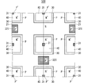
- FIG. 3 is a plan view schematically showing an example of a configuration of a semiconductor device according to an embodiment when an upper electrode and a dielectric film formed after semiconductor element formation are omitted.
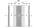
- FIG. 3 is a plan view schematically showing an example of a configuration of a semiconductor device according to an embodiment when unit cells are arranged in a comb shape.
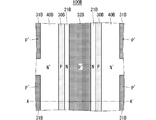
- FIG. 11 is a plan view schematically showing an example of a configuration of a semiconductor device according to an embodiment when unit cells are arranged in a ladder shape.
- FIG. 1 is a cross-sectional view schematically showing an example of a configuration of an IGBT as a semiconductor device according to an embodiment.
- FIG. 3 is a plan view schematically showing an example of a configuration of a semiconductor device according to an embodiment when an upper electrode and a dielectric film formed after semiconductor element formation are omitted.
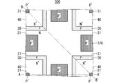
- FIG. 3
- FIG. 11 is a plan view schematically showing an example of a configuration of a semiconductor device according to an embodiment when unit cells are arranged in a stripe shape.
- FIG. 2 is a cross-sectional view schematically illustrating an example of a configuration of an IGBT according to the embodiment.
- FIG. 2 is a cross-sectional view schematically illustrating an example of a configuration of an IGBT according to the embodiment.
- FIG. 2 is a cross-sectional view schematically illustrating an example of a configuration of an IGBT according to the embodiment.
- FIG. 3 is a plan view schematically showing an example of a configuration of a semiconductor device according to an embodiment when an upper electrode and a dielectric film formed after semiconductor element formation are omitted.
- FIG. 2 is a cross-sectional view schematically illustrating an example of a configuration of an IGBT according to the embodiment.
- FIG. 3 is a plan view schematically showing an example of a configuration of a semiconductor device according to an embodiment when an upper electrode and a dielectric film formed after semiconductor element formation are omitted.
- FIG. 2 is a cross-sectional view schematically illustrating an example of a configuration of an IGBT according to the embodiment.
- FIG. 3 is a plan view schematically showing an example of a configuration of a semiconductor device according to an embodiment when an upper electrode and a dielectric film formed after semiconductor element formation are omitted.
- FIG. 3 is a plan view schematically showing an example of a configuration of a semiconductor device according to an embodiment when an upper electrode and a dielectric film formed after semiconductor element formation are omitted.
- FIG. 3 is a plan view schematically showing an example of a configuration of a semiconductor device according to an embodiment when an upper electrode and a dielectric film formed after semiconductor element formation are omitted.
- FIG. 2 is a cross-sectional view schematically illustrating an example of a configuration of an IGBT according to the embodiment.
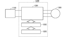
- 1 is a diagram conceptually illustrating an example of a configuration of a power conversion system including a power conversion device according to an embodiment.
- FIG. 1 is a sectional view schematically showing an example of the configuration of an IGBT 100 as a semiconductor device according to the present embodiment.
- FIG. 2 is a plan view schematically showing an example of the configuration of the semiconductor device according to the present embodiment when the upper electrode and the dielectric film formed after the formation of the semiconductor element are omitted.
- FIG. 1 corresponds to a section taken along the line AA ′ in FIG.
- FIG. 2 illustrates an example in which the unit cells are arranged in a lattice shape.
- the arrangement of the unit cells may also be a case where the unit cells are arranged in a comb shape, a case where the unit cells are arranged in a ladder shape, or It is also assumed that they are arranged in stripes.
- FIG. 3 is a plan view schematically showing an example of the configuration of the semiconductor device according to the present embodiment when the unit cells are arranged in a comb shape.
- FIG. 4 is a plan view schematically showing an example of the configuration of the semiconductor device according to the present embodiment when the unit cells are arranged in a ladder shape.
- FIG. 5 is a plan view schematically showing an example of the configuration of the semiconductor device according to the present embodiment when the unit cells are arranged in a stripe shape.
- FIG. 1 corresponds to a cross section taken along line A-A ′ in each of FIGS. 3, 4, and 5.
- the IGBT 100 includes a P-type collector region 10 having a relatively high concentration (P + ) of P-type impurities and one main surface of the collector region 10 (that is, the upper surface). And an N-type charge accumulation region 21 laminated on the upper surface of the drift region 20.
- the charge accumulation region 21 has a higher impurity concentration than the drift region 20.
- the semiconductor material used for the IGBT 100 is a wide band gap semiconductor having a larger band gap than a silicon semiconductor, and may be, for example, silicon carbide.
- a wide band gap semiconductor generally refers to a semiconductor having a forbidden band width of about 2 eV or more, a group 3 nitride such as gallium nitride (GaN), a group 2 oxide such as zinc oxide (ZnO), and selenium.
- Group 2 chalcogenides such as zinc oxide (ZnSe), diamond, and silicon carbide (SiC) are known.
- SiC silicon carbide
- a planar gate type SiC-IGBT in which the channel region is formed perpendicular to the thickness direction of IGBT 100 (that is, the vertical direction in FIG. 1) will be described as an example.
- a plurality of base regions 30 made of a P-type wide band gap semiconductor are selectively provided.
- An emitter region 40 made of an N-type wide band gap semiconductor is formed on each surface layer of the base region 30 at a position inside the outer periphery of the base region 30 at a predetermined interval.
- the emitter region 40 has a higher impurity concentration than the charge storage region 21.
- a well contact region 31 made of a low-resistance P-type wide band gap semiconductor is formed inside each emitter region 40.
- Well contact region 31 is formed to reach base region 30 from the upper surface of emitter region 40.
- a charge extraction region 32 made of a P-type wide band gap semiconductor is formed so as to be separated from the base region 30.
- the charge extraction region 32 has a higher impurity concentration than the base region 30.
- An ohmic electrode 70 is formed over a part of the upper surface of the emitter region 40 and a part of the upper surface of the well contact region 31.
- the ohmic electrode 70 is in ohmic connection with the wide band gap semiconductor.
- Schottky electrode 71 is formed on the upper surface of the charge extraction region 32. Schottky electrode 71 is Schottky-connected to P-type silicon carbide semiconductor layer (charge extraction region 32).
- the rising voltage when a forward voltage is applied to the Schottky connection is set to be, for example, 0.2 V or more and 2.0 V or less.
- the rising voltage may be, for example, 1.0 V.
- the gate insulating film 50 is formed over the upper surface of the base region 30 and the upper surface of the charge extraction region 32. Gate insulating film 50 is formed in contact with base region 30 at a position sandwiched between charge storage region 21 and emitter region 40. Further, a gate electrode 60 is formed via a gate insulating film 50 at a position overlapping the base region 30 in plan view. Further, an interlayer insulating film 55 is formed to cover the gate electrode 60.
- the emitter electrode 80 is formed so as to cover the open upper surface of the ohmic electrode 70, the open upper surface of the Schottky electrode 71, and the upper surface of the interlayer insulating film 55.
- the emitter electrode 80 is electrically connected to the ohmic electrode 70 and the Schottky electrode 71.
- An interlayer insulating film 55 is formed between the emitter electrode 80 and the gate electrode 60.
- a collector electrode 81 is formed on the lower surface of the collector region 10.
- FIG. 2 is a plan view schematically showing an example of the configuration of the semiconductor device according to the present embodiment.
- the IGBT 100 has an emitter region 40 surrounding the well contact region 31. Further, a base region 30 is formed surrounding the emitter region 40. Further, a charge storage region 21 is formed surrounding the base region 30.
- Each cell region is two-dimensionally arranged in the horizontal direction and the vertical direction in FIG.
- a charge extraction region 32 is formed in a region where a cell region is not formed.
- the charge extraction region 32 is formed in a region extending in the left-right direction where no cell region is formed and a region extending in the vertical direction where no cell region is formed.
- FIG. 3 is a plan view schematically showing an example of the configuration of the semiconductor device according to the present embodiment when the unit cells are arranged in a comb shape.
- an emitter region 40A is formed with a well contact region 31A interposed therebetween.
- base region 30A is formed with emitter region 40A interposed therebetween.
- a charge accumulation region 21A is formed with the base region 30A interposed therebetween.
- the comb-shaped cell regions thus formed are formed apart from each other, and a charge extraction region 32A is formed in a region between the cell regions.
- FIG. 4 is a plan view schematically showing an example of the configuration of the semiconductor device according to the present embodiment when the unit cells are arranged in a ladder shape.
- the emitter region 40B is formed with the well contact region 31B formed intermittently in the longitudinal direction.
- base region 30B is formed with emitter region 40B interposed therebetween.
- the charge accumulation region 21B is formed with the base region 30B interposed therebetween.
- the ladder-shaped cell regions thus formed are formed apart from each other, and a charge extraction region 32B is formed in a region between the cell regions.
- FIG. 5 is a plan view schematically showing an example of a configuration of a semiconductor device according to the present embodiment when unit cells are arranged in a stripe shape.
- an emitter region 40C is formed with a well contact region 31C formed intermittently in the longitudinal direction.
- the base region 30C is formed in partial contact with the well contact region 31C while sandwiching the emitter region 40C.
- a charge storage region 21C is formed with the base region 30C interposed therebetween.
- the stripe-shaped cell regions thus formed are formed apart from each other, and a charge extraction region 32C is formed in a region between the cell regions.
- an impurity concentration is, for example, 5 ⁇ 10 13 cm ⁇ 3 or more and 1 ⁇ 10 15 cm ⁇ 3 or less, for example, on the upper surface of the collector region 10 by a chemical vapor deposition (CVD) method.
- CVD chemical vapor deposition
- a drift region 20 made of N-type silicon carbide having a thickness of, for example, 50 ⁇ m or more and 200 ⁇ m or less is epitaxially grown.
- collector region 10 is a (0001) plane in which the plane orientation of the first main surface has an off angle, and is made of P-type, low-resistance silicon carbide having a 4H polytype. .
- the charge accumulation region 21 having an impurity concentration of, for example, 1 ⁇ 10 15 cm ⁇ 3 or more and 1 ⁇ 10 17 cm ⁇ 3 or less, and a film thickness of, for example, 1 ⁇ m or more and 10 ⁇ m or less, Epitaxial growth is performed on the upper surface of the drift region 20.
- an injection mask is formed in a predetermined region on the upper surface of the charge accumulation region 21 by using a photoresist or the like. Then, Al (aluminum), which is a P-type impurity, is ion-implanted.
- the depth of the Al ion implantation is, for example, 0.5 ⁇ m or more and 3 ⁇ m or less.
- the impurity concentration of ion-implanted Al is, for example, in the range of 1 ⁇ 10 17 cm ⁇ 3 or more and 1 ⁇ 10 19 cm ⁇ 3 or less, and the impurity concentration of the charge storage region 21 (first impurity Concentration) (second impurity concentration).
- the implantation mask is removed.
- the region into which Al has been ion-implanted becomes the base region 30.
- the depth of the Al ion implantation is, for example, 0.5 ⁇ m or more and 3 ⁇ m or less.
- the impurity concentration of ion-implanted Al is, for example, in the range of 1 ⁇ 10 17 cm ⁇ 3 or more and 1 ⁇ 10 19 cm ⁇ 3 or less, and the impurity concentration of the charge storage region 21 (first impurity Concentration) and higher than the impurity concentration of the base region 30 (second impurity concentration).
- the implantation mask is removed.
- the region into which Al is ion-implanted becomes the well contact region 31 and the charge extraction region 32.
- the width of the charge extraction region 32 when viewed in the section A-A ′ in FIG. 2 is, for example, 0.3 times or more and 0.5 times or less the width of the base region 30.
- N nitrogen
- the ion implantation depth of N is smaller than the thickness of the base region 30.
- the impurity concentration of the ion-implanted N is, for example, in the range of 1 ⁇ 10 18 cm ⁇ 3 or more and 1 ⁇ 10 21 cm ⁇ 3 or less, and the P-type impurity concentration of the base region 30 (second impurity). Impurity concentration).
- the region showing N-type among the regions into which N has been implanted becomes the emitter region 40.
- annealing is performed in a temperature range of, for example, 1300 ° C. or more and 1900 ° C. or less, for example, for 30 seconds or more and 1 hour or less in an inert gas atmosphere such as an argon (Ar) gas using a heat treatment apparatus.
- an inert gas atmosphere such as an argon (Ar) gas
- the ion-implanted Al and N are electrically activated.
- a field insulating film made of silicon dioxide of 5 ⁇ m or more and 2 ⁇ m or less is formed.
- the field insulating film at a position substantially corresponding to the active region may be removed by photolithography or etching.
- a silicon oxide film that is a gate insulating film 50 having a desired thickness is formed by thermally oxidizing the surface of the silicon carbide semiconductor layer that is not covered with the field insulating film.
- a polycrystalline silicon film having conductivity is formed on the upper surface of the gate insulating film 50 and the upper surface of the field insulating film by using a low-pressure CVD method.
- the gate electrode 60 is formed by patterning the formed polycrystalline silicon film.
- an interlayer insulating film 55 made of silicon oxide is formed by using a low pressure CVD method.
- a metal film containing Ni as a main component is formed in the contact hole by a sputtering method or the like. Thereafter, for example, heat treatment is performed at a temperature of not less than 600 ° C. and not more than 1100 ° C. to cause the metal film containing Ni as a main component to react with the silicon carbide semiconductor layer in the contact hole, thereby forming a silicon carbide semiconductor layer. Silicide is formed between the gate electrode and the metal film.
- the remaining metal film other than the silicide formed by the heat treatment is removed by wet etching.
- the ohmic electrode 70 is formed by the silicide thus formed.
- a metal film containing Al and Ti as main components is formed on the lower surface of the collector region 10, and a heat treatment is performed. By doing so, a back ohmic electrode (not shown here) is formed on the back side of the collector region 10.
- the interlayer insulating film 55 and the gate insulating film 50 on the upper surface of the charge extraction region 32 are removed by using patterning with a photoresist or the like.
- a metal film to be the Schottky electrode 71 is deposited by a sputtering method or the like, and the Schottky electrode 71 is formed on the upper surface of the charge extraction region 32 in the contact hole by patterning with a photoresist or the like.
- the metal film serving as the Schottky electrode 71 may be formed as a single-layer film containing Al, Mo, Au, Ti, Ni, V, or the like, or may be formed as a multilayer film in which these are combined. Good.
- a wiring metal such as Al is formed on the surface of the element thus far processed by sputtering or vapor deposition. Then, by processing the wiring metal into a predetermined shape by photolithography technology, an emitter electrode 80 that contacts the ohmic electrode 70 and the Schottky electrode 71 on the emitter side is formed, and a gate that contacts the gate electrode 60 is formed. A pad and a gate wiring are formed.
- the IGBT 100 shown in FIG. 1 can be obtained.
- the first state is a state in which a positive voltage is applied to the collector electrode 81 with respect to the emitter electrode 80 and a positive voltage equal to or higher than the threshold value is applied to the gate electrode 60. Call.
- a Schottky barrier diode (SBD) formed between the charge extraction region 32 and the Schottky electrode 71 has a threshold voltage (for example, SBD) although a forward voltage is applied to the Schottky barrier diode (SBD). 1.0V). Therefore, no current flows in the relevant location.
- SBD Schottky barrier diode
- Electrons flowing from the emitter electrode 80 to the collector electrode 81 are supplied from the ohmic electrode 70, the emitter region 40, the base region 30, the charge storage region 21 from the emitter electrode 80 in accordance with an electric field formed by a positive voltage applied to the collector electrode 81. , Drift region 20, and further, through collector region 10, to reach collector electrode 81.
- the holes flowing from the collector electrode 81 to the emitter electrode 80 are separated from the collector region 81, the drift region 20, the charge storage region 21, and the base region 30 in accordance with the electric field formed by the positive voltage applied to the collector electrode 81. , The emitter region 40, and further reach the emitter electrode 80 via the ohmic electrode 70.
- the structure according to the present embodiment can lower the on-resistance as compared with the case where the charge storage region 21 is not formed.
- the voltage applied between the emitter electrode 80 and the collector electrode 81 is called an on-voltage, and the value obtained by dividing the on-voltage by the density of the on-current is called an on-resistance.
- the on-resistance is equal to the sum of the resistances of the paths through which the electrons and holes flow.
- the product of the square of the on-current and the on-resistance is equal to the conduction loss consumed by the IGBT during conduction. Therefore, the on-resistance is preferably low.
- the ON current flows only through the active region where the channel region exists, and does not flow through the termination region and the invalid region other than the active region.
- the second state is a case where a high voltage is applied to the collector electrode 81 with respect to the emitter electrode 80 and a voltage equal to or lower than the threshold value is applied to the gate electrode 60, which is hereinafter referred to as an “off state”.
- the voltage of the gate electrode 60 is substantially equal to the voltage of the emitter electrode 80, a high voltage is applied between the gate electrode 60 and the collector electrode 81.
- a reverse bias is applied to the PN junction formed between the base region 30 and the charge storage region 21 in the active region, and the PN junction is thicker toward the charge storage region 21 and the drift region 20 having relatively low concentrations.
- the depletion layer spreads.
- application of a high voltage to the gate insulating film 50 is suppressed.
- the third state is a transition from the ON state to the OFF state, and is hereinafter referred to as a “turn-off transition period”.
- a mode for example, a latch-up mode
- IGBT IGBT
- the width of the carrier when passing through the junction / field / effect / transistor (JFET) region is reduced, but the JFET region is higher than the drift region 20 by the charge accumulation region 21. Because of the concentration, the conductivity can be kept low.
- the structure having the Schottky connection is formed in the same cell as the base region 30, the integration of the element is smaller than in the case where a rectifying element as shown in Patent Document 1 is formed outside the cell. It becomes possible. Therefore, the resistance per unit area can be reduced.
- the gate insulating film 50 Reliability is improved.
- the depletion layer extending from the charge extraction region 32 is connected to the depletion layer extending from the base region 30 and expands, and the electric field that tends to concentrate on the corner between the lower surface and the side surface of the base region 30 is dispersed. As a result, the avalanche voltage can be increased.
- the built-in voltage of the PN junction formed at the interface between emitter region 40 and base region 30 is, for example, 2.5 V.
- the value of the built-in voltage of the Schottky junction formed between the Schottky electrode 71 and the charge extraction region 32 is, for example, a value larger than 1.0 V.
- holes are generally discharged by a Schottky junction having a lower built-in voltage than a PN junction. Since the PN junction and the Schottky connection are connected in parallel, the Schottky connection becomes conductive before a voltage of 2.5 V is applied to the PN junction. Therefore, a voltage of, for example, 1.0 V or more is not applied to the PN connection due to a voltage drop in the drift region 20 or the like. As a result, since the PN junction does not operate and the latch-up mode does not occur, the latch-up tolerance increases.
- FIG. 6 is a sectional view schematically showing an example of the configuration of IGBT 200 according to the present embodiment. As illustrated in FIG. 6, the IGBT 200 has a similar configuration to the IGBT 100 illustrated as an example in the first embodiment.
- the IGBT 200 includes the collector region 10, the drift region 20, and the charge storage region 21.
- a trench gate type SiC-IGBT in which the channel region is formed horizontally with respect to the thickness direction of IGBT 200 (that is, the vertical direction in FIG. 6) will be described as an example.
- a plurality of base regions 30D made of a P-type wide band gap semiconductor are provided on the surface layer of the charge storage region 21.
- An emitter region 40D made of an N-type wide band gap semiconductor is formed on each surface layer of the base region 30D.
- a well contact region 31D made of a low-resistance P-type wide band gap semiconductor is formed inside each emitter region 40D.
- the trench 210 is formed from the upper surface of the emitter region 40D to a position deeper than the base region 30D.
- the gate insulating film 50D is formed in the trench 210 so as to cover the side surface of the base region 30D sandwiched between the charge storage region 21 and the emitter region 40D.
- a Schottky electrode 71D is formed on the upper surface of the charge extraction region 32D. Schottky electrode 71D is Schottky-connected to P-type silicon carbide semiconductor layer (charge extraction region 32D).
- the rising voltage when a forward voltage is applied to the Schottky connection is set to be, for example, 0.2 V or more and 2.0 V or less.
- the rising voltage may be, for example, 1.0 V.
- the trench 210 extends from the upper surface of the emitter region 40D, penetrates the emitter region 40D, and reaches a position deeper than the lower surface of the base region 30D and the lower surface of the charge extraction region 32D.
- An insulating film 50D is formed.
- the charge extraction region 32D is formed between the adjacent trenches 210. Although the charge extraction region 32D in FIG. 6 is formed in contact with the trench 210, the charge extraction region 32D may be formed separately from the trench 210.
- ⁇ Gate electrode 60 ⁇ / b> D surrounded by gate insulating film 50 ⁇ / b> D is formed in trench 210. Further, an interlayer insulating film 55D is formed on the upper surface of the gate electrode 60D.
- the emitter electrode 80D is electrically connected to the emitter region 40D, the well contact region 31D, and the Schottky electrode 71D.
- An interlayer insulating film 55D is formed between the emitter electrode 80D and the gate electrode 60D.
- a collector electrode 81 is formed on the lower surface of the collector region 10.
- holes are generally discharged by a Schottky junction having a lower built-in voltage than a PN junction. Since the PN junction and the Schottky connection are connected in parallel, the Schottky connection becomes conductive before a voltage of 2.5 V is applied to the PN junction. Therefore, a voltage of 1.0 V or more is not applied to the PN connection due to a voltage drop in the drift region 20 or the like. As a result, since the PN junction does not operate and the latch-up mode does not occur, the latch-up tolerance increases.
- the pitch per unit cell (cell pitch) can be reduced. Therefore, unit cells can be integrated for a limited device area, and a low on-resistance can be realized in an on state.
- FIG. 7 is a sectional view schematically showing an example of the configuration of IGBT 201 according to the present embodiment. As illustrated in FIG. 7, the IGBT 201 has a similar configuration to the IGBT 200 illustrated in the first embodiment.
- the IGBT 201 includes the collector region 10, the drift region 20, and the charge storage region 21.
- a trench gate type SiC-IGBT in which a channel region is formed horizontally with respect to the thickness direction of IGBT 201 (that is, the vertical direction in FIG. 7) will be described as an example.
- a plurality of base regions 30D are provided on the surface layer of the charge storage region 21.
- An emitter region 40D is formed on each surface layer of the base region 30D.
- a well contact region 31D is formed inside each emitter region 40D.
- a Schottky electrode 71E is formed on the side surface of the charge extraction region 32E opposite to the trench 210. Schottky electrode 71E is Schottky-connected to P-type silicon carbide semiconductor layer (charge extraction region 32E).
- the rising voltage when a forward voltage is applied to the Schottky connection is set to be, for example, 0.2 V or more and 2.0 V or less.
- the rising voltage may be, for example, 1.0 V.
- the trench 210 penetrates the emitter region 40D from the upper surface of the charge storage region 21 and further reaches a position deeper than the lower surface of the base region 30D and the lower surface of the charge extraction region 32E.
- a gate insulating film 50D is formed.
- the charge extraction region 32E is formed between the adjacent trenches 210. Although the charge extraction region 32E in FIG. 7 is formed in contact with the trench 210, the charge extraction region 32E may be formed apart from the trench 210.
- ⁇ Gate electrode 60 ⁇ / b> D surrounded by gate insulating film 50 ⁇ / b> D is formed in trench 210. Further, an interlayer insulating film 55D is formed on the upper surface of the gate electrode 60D.
- the upper surface of the opened emitter region 40D, the opened upper surface of the well contact region 31D, the opened side surface of the Schottky electrode 71E, and the upper surface of the interlayer insulating film 55D are covered with the emitter.
- An electrode 80E is formed.
- the emitter electrode 80E is formed in a dummy trench 220 formed from the upper surface of the charge extraction region 32E and penetrating the charge extraction region 32E.
- the Schottky electrode 71E is formed on the side surface of the charge extraction region 32E in the dummy trench 220.
- the emitter electrode 80E is electrically connected to the emitter region 40D, the well contact region 31D, and the Schottky electrode 71E in the dummy trench 220.
- An interlayer insulating film 55D is formed between the emitter electrode 80E and the gate electrode 60D.
- a collector electrode 81 is formed on the lower surface of the collector region 10.
- the Schottky electrode 71E is formed horizontally with respect to the thickness direction of the IGBT 201.
- the size (specifically, depth, width, and depth) of the dummy trench 220 can be changed as appropriate.
- the size of the dummy trench 220 may be the same as the size of the trench 210 including the gate electrode 60D.
- holes are generally discharged by a Schottky junction having a lower built-in voltage than a PN junction. Since the PN junction and the Schottky connection are connected in parallel, the Schottky connection becomes conductive before a voltage of 2.5 V is applied to the PN junction. Therefore, a voltage of 1.0 V or more is not applied to the PN connection due to a voltage drop in the drift region 20 or the like. As a result, since the PN junction does not operate and the latch-up mode does not occur, the latch-up tolerance increases.
- the planar size of the charge extraction region 32E can be reduced. Therefore, the pitch per unit cell (cell pitch) can be reduced. As a result, unit cells can be integrated for a limited device area, and a low on-resistance can be realized in an on-state.
- ⁇ Third embodiment> A wide band gap semiconductor device and a method of manufacturing the wide band gap semiconductor device according to the present embodiment will be described.
- the same components as those described in the above-described embodiment will be denoted by the same reference numerals, and detailed description thereof will be omitted as appropriate. .
- the charge storage region 21 is formed on the entire upper surface of the drift region 20 by epitaxial growth.
- the manner of forming the charge storage region is not limited to such a case.
- FIG. 8 is a cross-sectional view schematically showing an example of the configuration of IGBT 202 according to the present embodiment.
- the IGBT 202 includes the collector region 10, the drift region 20, and the charge storage region 21F partially laminated on the upper surface of the drift region 20.
- a plurality of base regions 30 are provided on the surface layer of the charge storage region 21F.
- An emitter region 40 is formed on each surface layer of the base region 30.
- a well contact region 31 is formed inside each emitter region 40.
- a charge extraction region 32 is formed on the surface layer of the charge accumulation region 21F.
- the charge accumulation region 21 ⁇ / b> F is formed on the upper surface of the drift region 20 with the N-type separation region 22 in contact immediately below a part of the charge extraction region 32.
- the impurity concentration of N-type separation region 22 is, for example, equal to the impurity concentration of drift region 20.
- An ohmic electrode 70 is formed over a part of the upper surface of the emitter region 40 and a part of the upper surface of the well contact region 31. Further, a Schottky electrode 71 is formed on the upper surface of the charge extraction region 32.
- the rising voltage when a forward voltage is applied to the Schottky connection is set to be, for example, 0.2 V or more and 2.0 V or less.
- the rising voltage may be, for example, 1.0 V.
- the gate insulating film 50 is formed over the upper surface of the base region 30 and the upper surface of the charge extraction region 32. Further, a gate electrode 60 is formed via a gate insulating film 50 at a position overlapping the base region 30 in plan view. Further, an interlayer insulating film 55 is formed to cover the gate electrode 60.
- the emitter electrode 80 is formed so as to cover the open upper surface of the ohmic electrode 70, the open upper surface of the Schottky electrode 71, and the upper surface of the interlayer insulating film 55.
- a collector electrode 81 is formed on the lower surface of the collector region 10.
- the method of forming the charge storage region 21F is not limited to epitaxial growth.
- an implantation mask is formed on the upper surface of the drift region 20 by using a photoresist or the like at a position where the N-type separation region 22 is to be formed. Then, N, which is an N-type impurity, is ion-implanted. At this time, the depth of the N ion implantation is, for example, not less than 1.0 ⁇ m and not more than 3 ⁇ m. After that, the implantation mask is removed.
- the region into which the N ions are implanted becomes the charge storage region 21F, and the region into which the N ions are not implanted becomes the N-type separation region 22.
- dV / dt is extremely large during the turn-off transition period, for example, 2.5 V is applied to the PN junction formed at the interface between the emitter region 40 and the base region 30 having the structure shown in FIG.
- the above voltage drop may occur, and a latch-up mode may occur.
- the N-type separation region 22 is formed immediately below a part of the charge extraction region 32, so that the potential wall at the interface between the drift region 20 and the charge accumulation region 21F is reduced. Reduced. Therefore, many holes flow to the Schottky connection during the transitional period of turn-off, so that the latch-up tolerance can be increased.
- FIG. 9 is a plan view schematically showing an example of the configuration of the semiconductor device according to the present embodiment when the upper electrode and the dielectric film formed after the formation of the semiconductor element are omitted.
- the IGBT 300 has an emitter region 40 surrounding the well contact region 31. Further, a base region 30 is formed surrounding the emitter region 40. Further, a charge storage region 21 is formed surrounding the base region 30.
- Each cell region is two-dimensionally arranged in the horizontal direction and the vertical direction in FIG.
- a charge extraction region 32G is formed in a region where no cell region is formed.
- the charge extraction region 32G includes a region extending in the left-right direction where no cell region is formed, and a region extending in the left-right direction where no cell region is formed, except for an intersection region between a region extending in the left-right direction where no cell region is formed and a region extending in the vertical direction where no cell region is formed. And a region extending in the vertical direction that is not formed.
- the charge extraction region 32G is formed between the nearest cell regions (that is, between the upper and lower cell regions in FIG. 9 and between the left and right cell regions in FIG. 9), It is not formed between diagonally located cell regions in plan view.
- FIG. 10 is a cross-sectional view schematically showing an example of the configuration of IGBT 300 according to the present embodiment.
- FIG. 10 corresponds to a B-B ′ section in FIG. 9 is the same as the structure shown in FIG. 1 except that the charge extraction region 32 is replaced by the charge extraction region 32G.
- the IGBT 300 includes the collector region 10, the drift region 20, and the charge storage region 21.
- a plurality of base regions 30 are provided on the surface layer of the charge storage region 21.
- An emitter region 40 is formed on each surface layer of the base region 30.
- a well contact region 31 is formed inside each emitter region 40.
- An ohmic electrode 70 is formed over a part of the upper surface of the emitter region 40 and a part of the upper surface of the well contact region 31.
- the gate insulating film 50 is formed over the upper surface of the base region 30. Further, a gate electrode 60 is formed via a gate insulating film 50 at a position overlapping the base region 30 in plan view. Further, an interlayer insulating film 55 is formed to cover the gate electrode 60.
- the emitter electrode 80 is formed to cover the open upper surface of the ohmic electrode 70 and the upper surface of the interlayer insulating film 55.
- Emitter electrode 80 is electrically connected to ohmic electrode 70.
- An interlayer insulating film 55 is formed between the emitter electrode 80 and the gate electrode 60.
- a collector electrode 81 is formed on the lower surface of the collector region 10.
- the charge extraction region 32G is formed near the base region 30. Therefore, the amount of holes flowing to the base region 30 can be reduced. Therefore, the latch-up tolerance can be increased.
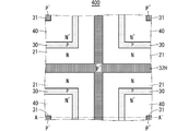
- FIG. 11 is a plan view schematically showing an example of the configuration of the semiconductor device according to the present embodiment when the upper electrode and the dielectric film formed after the formation of the semiconductor element are omitted.
- the IGBT 400 has the emitter region 40 surrounding the well contact region 31. Further, a base region 30 is formed surrounding the emitter region 40. Further, a charge storage region 21 is formed surrounding the base region 30.
- the respective cell regions thus formed are formed apart from each other.
- the respective cell regions are two-dimensionally arranged in the horizontal direction and the vertical direction in FIG.
- a charge extraction region 32H is formed in a region where no cell region is formed.
- the charge extracting region 32H is formed in a region extending in the left-right direction where no cell region is formed and a region extending in the vertical direction where no cell region is formed.
- the charge extraction region 32H has a smaller area in plan view than the charge extraction region 32 in FIG. 2, for example. Specifically, the charge extraction region 32H is formed only in a part in the width direction of a region extending in the left-right direction where no cell region is formed, and has a smaller width than the charge extraction region 32 in FIG. Similarly, the charge extraction region 32H is formed only in a part in the width direction of the region extending in the vertical direction where the cell region is not formed, and has a smaller width than the charge extraction region 32 in FIG.
- the area of the region where the charge extraction region 32H is formed is, for example, 0.05 times or more and 0.5 times or less of the sum of the areas of the base region 30, the emitter region 40, and the well contact region 31. I do.
- FIG. 12 is a cross-sectional view schematically showing an example of the configuration of IGBT 400 according to the present embodiment.
- FIG. 12 corresponds to a section taken along line A-A ′ in FIG.
- the IGBT 400 includes the collector region 10, the drift region 20, and the charge storage region 21.
- a plurality of base regions 30 are provided on the surface layer of the charge storage region 21.
- An emitter region 40 is formed on each surface layer of the base region 30.
- a well contact region 31 is formed inside each emitter region 40.
- a charge extraction region 32H made of a P-type wide band gap semiconductor is formed so as to be separated from the base region 30.
- An ohmic electrode 70 is formed over a part of the upper surface of the emitter region 40 and a part of the upper surface of the well contact region 31.
- a Schottky electrode 71H is formed on the upper surface of the charge extraction region 32H.
- Schottky electrode 71H is Schottky-connected to P-type silicon carbide semiconductor layer (charge extraction region 32H).
- the rising voltage when a forward voltage is applied to the Schottky connection is set to be, for example, 0.2 V or more and 2.0 V or less.
- the rising voltage may be, for example, 1.0 V.
- the gate insulating film 50 is formed over the upper surface of the base region 30 and the upper surface of the charge extraction region 32H. Further, a gate electrode 60 is formed via a gate insulating film 50 at a position overlapping the base region 30 in plan view. Further, an interlayer insulating film 55 is formed to cover the gate electrode 60.
- An emitter electrode 80H is formed to cover the upper surface of the opened ohmic electrode 70, the upper surface of the opened Schottky electrode 71H, and the upper surface of the interlayer insulating film 55.
- the emitter electrode 80H is electrically connected to the ohmic electrode 70 and the Schottky electrode 71H.
- An interlayer insulating film 55 is formed between the emitter electrode 80H and the gate electrode 60.
- a collector electrode 81 is formed on the lower surface of the collector region 10.
- the area of the region where the Schottky electrode 71H is formed in plan view is smaller than the area of the region where the ohmic electrode 70 is formed in plan view. Even if it is small, the effect of increasing the latch-up tolerance during the turn-off transition period can be obtained.
- FIG. 13 is a plan view schematically showing an example of the configuration of the semiconductor device according to the present embodiment when the upper electrode and the dielectric film formed after the formation of the semiconductor element are omitted.
- the IGBT 500 has an emitter region 40 surrounding the well contact region 31. Further, a base region 30 is formed surrounding the emitter region 40. Further, a charge storage region 21 is formed surrounding the base region 30.
- Each cell region is two-dimensionally arranged in the horizontal direction and the vertical direction in FIG.
- the charge extraction region 32I is formed in a region where no cell region is formed.
- the charge extraction region 32I is a portion of a region extending in the left-right direction where no cell region is formed, except for an intersection region between a region extending in the left-right direction where no cell region is formed and a region extending in the vertical direction where no cell region is formed, It is formed in a part of the region extending in the vertical direction where the region is not formed.
- the charge extraction region 32I is formed between the nearest cell regions (that is, between the upper and lower cell regions in FIG. 13 and between the left and right cell regions in FIG. 13). It is not formed between diagonally located cell regions in plan view.
- the charge extraction region 32I is formed only in a part of the regions between the nearest cell regions, and is not formed between all the nearest cell regions.
- FIG. 14 is a plan view schematically showing an example of the configuration of the semiconductor device according to the present embodiment when the upper electrode and the dielectric film formed after the formation of the semiconductor element are omitted.
- the IGBT 600 has the emitter region 40 surrounding the well contact region 31. Further, a base region 30 is formed surrounding the emitter region 40. Further, a charge storage region 21 is formed surrounding the base region 30. The cell regions thus formed are two-dimensionally spaced apart from each other, and a charge extraction region 32J is partially formed in a region between the cell regions.
- the charge extraction region 32J is disposed in a place where a cell region is formed, replacing the cell region. 14, the cell regions and the charge extraction regions 32J are alternately arranged in the up-down direction and the left-right direction in FIG.
- FIG. 15 is a cross-sectional view schematically showing an example of the configuration of IGBT 600 according to the present embodiment.
- FIG. 15 corresponds to a section taken along line C-C ′ in FIG.
- the IGBT 600 includes a collector region 10, a drift region 20, and a charge storage region 21.
- a base region 30 is provided on the surface layer of the charge storage region 21.
- An emitter region 40 is formed on the surface of the base region 30.
- a well contact region 31 is formed inside the emitter region 40.
- a charge extraction region 32J made of a P-type wide band gap semiconductor is formed so as to be separated from the base region 30.
- An ohmic electrode 70 is formed over a part of the upper surface of the emitter region 40 and a part of the upper surface of the well contact region 31.
- a Schottky electrode 71J is formed on the upper surface of the charge extraction region 32J. Schottky electrode 71J is Schottky-connected to P-type silicon carbide semiconductor layer (charge extraction region 32J).
- the rising voltage when a forward voltage is applied to the Schottky connection is set to be, for example, 0.2 V or more and 2.0 V or less.
- the rising voltage may be, for example, 1.0 V.
- a gate insulating film 50 is formed over the upper surface of the base region 30 and the upper surface of the charge extraction region 32J. Further, a gate electrode 60 is formed via a gate insulating film 50 at a position overlapping the base region 30 in plan view. Further, an interlayer insulating film 55 is formed to cover the gate electrode 60.
- the emitter electrode 80J is formed so as to cover the open upper surface of the ohmic electrode 70, the open upper surface of the Schottky electrode 71J, and the upper surface of the interlayer insulating film 55.
- the emitter electrode 80J is electrically connected to the ohmic electrode 70 and the Schottky electrode 71J.
- An interlayer insulating film 55 is formed between the emitter electrode 80J and the gate electrode 60.
- a collector electrode 81 is formed on the lower surface of the collector region 10.
- the semiconductor device according to the above-described embodiment is applied to a power converter.
- the power converter to be applied is not limited to a specific application, but a case where the power converter is applied to a three-phase inverter will be described below.
- FIG. 16 is a diagram conceptually showing an example of the configuration of a power conversion system including the power conversion device according to the present embodiment.
- the power conversion system includes a power supply 1100, a power conversion device 1200, and a load 1300.
- Power supply 1100 is a DC power supply, and supplies DC power to power converter 1200.
- the power supply 1100 can be composed of various types, and for example, can be composed of a DC system, a solar battery, a storage battery, or the like. Further, the power supply 1100 can be configured with a rectifier circuit or an AC-DC converter connected to an AC system. Further, power supply 1100 may be configured by a DC-DC converter that converts DC power output from a DC system into predetermined power.
- the power conversion device 1200 is a three-phase inverter connected between the power supply 1100 and the load 1300.
- the power converter 1200 converts DC power supplied from the power supply 1100 into AC power, and further supplies the AC power to the load 1300.
- the power conversion device 1200 converts a DC power into an AC power and outputs the converted power and a drive signal for driving each switching element of the conversion circuit 1201.
- the driving circuit 1202 includes an output driving circuit 1202 and a control circuit 1203 that outputs a control signal for controlling the driving circuit 1202 to the driving circuit 1202.
- the load 1300 is a three-phase electric motor driven by the AC power supplied from the power converter 1200.
- the load 1300 is not limited to a specific use, but is a motor mounted on various electric devices, for example, a motor used for a hybrid vehicle, an electric vehicle, a railway vehicle, an elevator, or an air conditioner. It is.
- the conversion circuit 1201 includes a switching element and a free wheel diode (not shown here).
- the switching element performs a switching operation, the DC power supplied from the power supply 1100 is converted into AC power, and is further supplied to the load 1300.
- the conversion circuit 1201 is a two-level three-phase full-bridge circuit, and includes six switching elements and each switching element. And six freewheel diodes connected in anti-parallel.
- the semiconductor device in any of the above-described embodiments is applied to at least one of each switching element and each freewheeling diode in the conversion circuit 1201.
- the six switching elements are connected in series every two switching elements to form upper and lower arms, and each upper and lower arm forms each phase (ie, U phase, V phase, and W phase) of the full bridge circuit.
- the output terminals of the upper and lower arms (that is, the three output terminals of the conversion circuit 1201) are connected to the load 1300.
- the drive circuit 1202 generates a drive signal for driving the switching element of the conversion circuit 1201, and further supplies the drive signal to the control electrode of the switching element of the conversion circuit 1201. Specifically, a drive signal for turning on the switching element and a drive signal for turning off the switching element are output to control electrodes of the respective switching elements based on a control signal output from a control circuit 1203 described later. I do.
- the drive signal is a voltage signal higher than the threshold voltage of the switching element (that is, ON signal).
- the drive signal is lower than the threshold voltage of the switching element. (That is, an off signal).
- the control circuit 1203 controls the switching element of the conversion circuit 1201 so that desired power is supplied to the load 1300. Specifically, based on the power to be supplied to the load 1300, a time during which each switching element of the conversion circuit 1201 is to be turned on (that is, an on-time) is calculated. For example, the conversion circuit 1201 can be controlled by PWM control that modulates the ON time of the switching element according to the voltage to be output.
- control circuit 1203 issues a control command to the drive circuit 1202 such that an ON signal is output to the switching element to be turned on at each time and an OFF signal is output to the switching element to be turned off at each time. That is, a control signal is output.
- the drive circuit 1202 outputs an ON signal or an OFF signal as a drive signal to a control electrode of each switching element based on the control signal.
- the semiconductor device according to any of the above-described embodiments is applied as a switching element of the conversion circuit 1201. Therefore, it is possible to stabilize the on-resistance after an energization cycle. it can.
- the semiconductor device in any of the embodiments described above may be applied to a three-level or multi-level power converter.
- the semiconductor device according to any of the above-described embodiments may be applied to a single-phase inverter.
- the semiconductor device in any of the above-described embodiments can be applied to a DC-DC converter or an AC-DC converter.
- the power converter to which the semiconductor device according to any of the embodiments described above is applied is not limited to the case where the load described above is an electric motor. It can also be used as a power supply for a cooking machine, induction heating cooker or non-contact power supply system.
- a power conversion device to which the semiconductor device in any of the above-described embodiments is applied can also be used as a power conditioner in a solar power generation system, a power storage system, or the like.
- the replacement may be made over a plurality of embodiments. That is, a configuration in which the same effects are obtained by combining the respective configurations illustrated in the different embodiments may be employed.
- the wide band gap semiconductor device includes the drift region 20 made of the first conductivity type (ie, N type) wide band gap semiconductor (for example, silicon carbide), and the drift region.
- a collector region 10 made of a second-conductivity-type (ie, P-type) wide bandgap semiconductor, a charge accumulation region 21 made of an N-type wide-bandgap semiconductor, and a P-type base formed on the lower surface of the base 20. It includes a region 30, a P-type charge extraction region 32, an N-type emitter region 40, a Schottky electrode 71, a gate insulating film 50, a gate electrode 60, an emitter electrode 80, and a collector electrode 81.
- the charge accumulation region 21 is formed on the upper surface of the drift region 20.
- the charge accumulation region 21 has a higher impurity concentration than the drift region 20.
- the base region 30 is partially formed in the surface layer of the charge storage region 21.
- the charge extraction region 32 is formed on the surface layer of the charge accumulation region 21 so as to be separated from the base region 30.
- the charge extraction region 32 has a higher impurity concentration than the base region 30.
- Emitter region 40 is partially formed in the surface layer of base region 30.
- the emitter region 40 has a higher impurity concentration than the charge storage region 21.
- the Schottky electrode 71 is formed in contact with the charge extraction region 32. Further, the Schottky electrode 71 is in Schottky connection with the charge extraction region 32.
- Gate insulating film 50 is formed in contact with base region 30 at a position sandwiched between charge storage region 21 and emitter region 40.
- Gate electrode 60 is formed in contact with gate insulating film 50.
- the emitter electrode 80 is formed to cover the Schottky electrode 71 and the emitter region 40.
- Collector electrode 81 is formed on the lower surface of collector region 10.
- the Schottky connection is conducted at a lower voltage than the PN connection at the interface between the base region and the emitter region, so that a voltage higher than the built-in voltage is not applied to the PN junction.
- the latch-up tolerance increases, and the reliability of the wide band gap semiconductor device improves.
- the structure having the Schottky connection is formed in the same cell as the base region 30, the elements can be integrated. Therefore, the resistance per unit area can be reduced.
- the built-in voltage of the Schottky barrier diode formed between Schottky electrode 71 and charge extraction region 32 is such that the built-in voltage is between base region 30 and emitter region 40. It is smaller than the built-in voltage of the diode formed.
- the Schottky connection becomes conductive before a voltage of 2.5 V is applied to the PN junction. Therefore, a voltage of, for example, 1.0 V or more is not applied to the PN connection due to a voltage drop in the drift region 20 or the like. As a result, since the PN junction does not operate and the latch-up mode does not occur, the latch-up tolerance increases.
- the wide band gap semiconductor device includes the N-type separation region 22 formed in contact with a part of the lower surface of the charge extraction region 32. Then, the impurity concentration of the separation region 22 is equal to the impurity concentration of the drift region 20. According to such a configuration, the N-type separation region 22 is formed directly below a part of the charge extraction region 32, so that the potential wall at the interface between the drift region 20 and the charge accumulation region 21F is reduced. . Therefore, many holes flow to the Schottky connection during the transitional period of turn-off, so that the latch-up tolerance can be increased.
- a plurality of base regions 30 are arranged on the surface layer of the charge storage region 21 in plan view.
- the plurality of base regions 30 are two-dimensionally arranged in a first direction and a second direction orthogonal to the first direction in plan view.
- the region extending in the first direction and the base region is not arranged is the first region, and the region extending in the second direction and the base region is not arranged is the second region, the charge extraction is performed.
- the region 32 is formed in the first region and the second region in plan view.
- the Schottky connection is conducted at a lower voltage than the PN connection at the interface between the base region and the emitter region, so that a voltage higher than the built-in voltage is not applied to the PN junction.
- the latch-up tolerance increases, and the reliability of the wide band gap semiconductor device improves.
- the charge extraction region 32H is formed in a part of the first region in the width direction and a part of the second region in the width direction in plan view. You. According to such a configuration, since the area in plan view of the region where the charge extraction region 32H is formed is smaller than the charge extraction region 32 in FIG. 2, for example, when carriers pass through the JFET region in the ON state. The width of the path widens.
- the wide bandgap semiconductor device includes the P-type well contact region 31 formed from the upper surface of the emitter region 40 to the base region 30.
- the area of the charge extraction region 32H in plan view is 0.05 times or more of the sum of the area of the base region 30, the area of the emitter region 40, and the area of the well contact region 31 in plan view, and 0.5 Less than twice. According to such a configuration, since the area in plan view of the region where the charge extraction region 32H is formed is smaller than the charge extraction region 32 in FIG. 2, for example, when carriers pass through the JFET region in the ON state. The width of the path increases. Therefore, the resistance of the JFET can be reduced.
- the area of the region where the Schottky electrode 71H is formed in plan view is smaller than the area of the region where the ohmic electrode 70 is formed in plan view. Even if it is small, the effect of increasing the latch-up tolerance during the turn-off transition period can be obtained.
- the first region extending in the first direction and having no base region is arranged, and the second region extending in the second direction and having no base region arranged.
- the charge extraction region 32G is formed in the first region and the second region excluding the intersection region in plan view.
- the region where the charge extraction region 32G is formed is limited to only between the cell regions located closest to each other (that is, in the vicinity of the base region 30 in FIG. 9). The width of the path when carriers pass through the JFET region is increased. Therefore, the resistance of the JFET can be reduced.
- the charge extraction region 32G is formed near the base region 30. Therefore, the amount of holes flowing to the base region 30 can be reduced. Therefore, the latch-up tolerance can be increased.
- the charge extraction region 32I is formed in a part of the first region and a part of the second region except the intersection region in plan view. According to such a configuration, the width of carriers passing through the JFET region in the ON state is increased. Therefore, the resistance of the JFET can be reduced. Further, since there is a large difference in the built-in voltage between the PN junction and the Schottky junction, even if the area of the region where the charge extracting region 32I is formed in a plan view is small, the effect of increasing the latch-up withstand voltage during the turn-off transition period is obtained. .
- a plurality of base regions 30 are arranged on the surface layer of the charge storage region 21 in plan view.
- the plurality of base regions 30 are two-dimensionally arranged in a first direction and a second direction orthogonal to the first direction in plan view.
- the charge extraction region 32J is formed by replacing a part of the plurality of base regions 30 arranged.
- the Schottky connection is conducted at a lower voltage than the PN connection at the interface between the base region and the emitter region, so that a voltage higher than the built-in voltage is not applied to the PN junction.
- the latch-up tolerance increases, and the reliability of the wide band gap semiconductor device improves.
- the wide bandgap semiconductor device includes trench 210 formed from the upper surface of emitter region 40D to a position deeper than base region 30D.
- the gate insulating film 50D is formed in the trench 210 so as to cover the side surface of the base region 30D sandwiched between the charge storage region 21 and the emitter region 40D.
- the gate electrode 60D is formed in the trench 210 so as to be surrounded by the gate insulating film 50D. According to such a configuration, the pitch per unit cell (cell pitch) can be reduced. Therefore, unit cells can be integrated for a limited device area, and a low on-resistance can be realized in an on state.
- the wide band gap semiconductor device includes the dummy trench 220 formed from the upper surface of the charge extraction region 32E to a position deeper than the charge extraction region 32E. Then, the emitter electrode 80E is also formed in the dummy trench 220. The Schottky electrode 71E is formed in the dummy trench 220. The Schottky electrode 71E is formed in contact with the side surface of the charge extraction region 32. According to such a configuration, Schottky electrode 71E is formed horizontally with respect to the thickness direction of IGBT 201. Therefore, the size of the dummy trench 220 can be appropriately changed. Further, the planar size of the charge extraction region 32E can be reduced. Therefore, the pitch per unit cell (cell pitch) can be reduced. As a result, unit cells can be integrated for a limited device area, and a low on-resistance can be realized in the on state.
- the wide band gap semiconductor is a silicon carbide semiconductor. According to such a configuration, it is possible to realize a semiconductor device with high withstand voltage, high frequency, and high output.
- the power conversion device includes the conversion circuit 1201, the drive circuit 1202, and the control circuit 1203.
- the conversion circuit 1201 has a wide band gap semiconductor device.
- the conversion circuit 1201 converts input power and outputs the converted power.
- the drive circuit 1202 outputs a drive signal for driving the wide band gap semiconductor device to the wide band gap semiconductor device.
- the control circuit 1203 outputs a control signal for controlling the drive circuit 1202 to the drive circuit 1202.
- the Schottky connection is conducted at a lower voltage than the PN connection at the interface between the base region and the emitter region, a voltage higher than the built-in voltage is not applied to the PN junction. As a result, the latch-up tolerance increases, and the reliability of the power conversion device improves. Further, since the structure having the Schottky connection is formed in the same cell as the base region, the elements can be integrated. Therefore, the resistance per unit area can be reduced.
- each component in the above-described embodiment is a conceptual unit, and one component includes a plurality of structures within the scope of the technology disclosed in this specification. And a case where one component corresponds to a part of a structure, and a case where a plurality of components are provided in one structure.
- each component in the above-described embodiment includes a structure having another structure or shape as long as the same function is exhibited.
- the material includes other additives, such as an alloy. Shall be included.
Landscapes
- Electrodes Of Semiconductors (AREA)
- Metal-Oxide And Bipolar Metal-Oxide Semiconductor Integrated Circuits (AREA)
Abstract
十分なラッチアップ耐量が得られ、かつ、集積化が可能となる技術を提供する。ワイドバンドギャップ半導体装置は、コレクタ領域(10)と、ドリフト領域よりも高い不純物濃度を有する電荷蓄積領域(21)と、ベース領域(30)と、ベース領域よりも高い不純物濃度を有する電荷引き抜き領域(32)と、エミッタ領域(40)と、ショットキー電極(71)と、ゲート絶縁膜(50)と、ゲート電極(60)と、エミッタ電極(80)と、コレクタ電極(81)とを備える。
Description
本願明細書に開示される技術は、ワイドバンドギャップ半導体装置、および、電力変換装置に関するものである。
ワイドバンドギャップ半導体のトランジスタは、主に金属-酸化膜-半導体電界効果トランジスタ(metal-oxide-semiconductor field-effect transistor、すなわち、MOSFET)型を主体として開発されている。しかしながら、超高耐圧下では導通損の低減が必要となるため、バイポーラ型のトランジスタが注目されている。絶縁ゲート型バイポーラトランジスタ(insulated gate bipolar transistor、すなわち、IGBT)では、低オン抵抗、低スイッチング損失、かつ、耐久性の高いデバイスが求められている。
IGBTにおいて、デバイスに不具合が発生するモードとして、主電流が流れているオン状態から、主電流が流れないオフ状態へ移行する際に、P型のベース領域に流れるホール電流による電圧降下が、N型の不純物を比較的高濃度(N+)で有するエミッタ領域とP型のベース領域との間のビルトイン電圧を超えてしまうと、寄生サイリスタがオン状態となり、さらに、電流が流れ続けるラッチアップ状態となって、デバイスの損傷に至るラッチアップモードが挙げられる。
また、主電流が流れているオン状態の場合に、P型のコレクタ領域からN型のドリフト領域に注入されたホールのほとんどがP型のベース領域へ抜けてしまうと、N型のドリフト領域内のキャリア濃度が増加されず、オン抵抗を下げることができない。
以上のように、オン状態においては、ホールをN型のドリフト領域内に蓄積し、オン状態からオフ状態へ移行する際は、P型のベース領域へ流れるホール電流を低減しなければならない。
このような問題に対して、たとえば特許文献1には、トレンチゲートを有するIGBTにおいて、主電流を流すメインセルの他に、ホール電流をエミッタ電極へ流すことができるダミーセルが形成されている。さらに、ダミーセルには、直列に接続された整流素子を有する構造が開示されている。
この構造においては、オン状態からオフ状態に移行する際にはダミーセルへホールが流れるため、ダミーセルと並列に接続されたメインセルのN型のエミッタ領域の直下を流れるホール電流は低減され、ラッチアップ耐量は増加する。
さらにオン状態においては、整流素子にビルトイン電圧(およそ0.7V)以下の電圧しか印加されないので、ホールは排出されない。よって、高いラッチアップ耐量と低いオン抵抗とを確保することができる。
特許文献1に開示された構成では、整流素子のビルトイン電圧はおよそ0.7Vであり、SiのPN接合のビルトインポテンシャルに相当する。
エミッタ領域とベース領域との間のPN接合がSiで形成された場合、このPN接合は、前述の整流素子と同じくビルトイン電圧が0.7V程度である。当該整流素子に0.7Vの電圧が印加されて導通する場合、エミッタ領域とベース領域との間のPN接合にも、0.7V程度の電圧が印加されて導通する可能性がある。
IGBTと整流素子とがSiCのPN接合で作成された場合も同様で、どちらのビルトイン電圧もおよそ2.5Vとなり、十分なラッチアップ耐量が得られない。
IGBTをSiCで作製し、整流素子をSiで作製することによってビルトイン電圧に差を付けることができるが、IGBTと整流素子とを密集させて形成することができないため、単位面積あたりの抵抗値を低減することができない。
また、特許文献1に開示された構成では、整流素子がデバイスの外部に設けられている。そのため、ダミーセル内のP型の領域と当該整流素子とを接続するために、ゲート電極またはエミッタ電極とは異なる電極(具体的には、ダイバータ電極)が必要となっている。
ダイバータ電極と整流素子とは、たとえば、ワイヤーボンディングなどの方法で接続される。そのため、ある程度面積の広い電極パッド(具体的には、ダイバータ電極パッド)がデバイス上に形成される必要があり、集積化が困難であった。
本願明細書に開示される技術は、以上に記載されたような問題を解決するためになされたものであり、十分なラッチアップ耐量が得られ、かつ、集積化が可能となる技術を提供することを目的とするものである。
本願明細書に開示される技術の第1の態様は、第1の導電型のワイドバンドギャップ半導体からなるドリフト領域と、前記ドリフト領域の下面に形成される、第2の導電型のワイドバンドギャップ半導体からなるコレクタ領域と、前記ドリフト領域の上面に形成され、かつ、前記ドリフト領域よりも高い不純物濃度を有する、第1の導電型のワイドバンドギャップ半導体からなる電荷蓄積領域と、前記電荷蓄積領域の表層において部分的に形成される、第2の導電型のベース領域と、前記電荷蓄積領域の表層において前記ベース領域から離間して形成され、かつ、前記ベース領域よりも高い不純物濃度を有する、第2の導電型の電荷引き抜き領域と、前記ベース領域の表層において部分的に形成され、かつ、前記電荷蓄積領域よりも高い不純物濃度を有する、第1の導電型のエミッタ領域と、前記電荷引き抜き領域に接触して形成され、かつ、前記電荷引き抜き領域とショットキー接続するショットキー電極と、前記電荷蓄積領域と前記エミッタ領域とに挟まれる位置の前記ベース領域に接触して形成されるゲート絶縁膜と、前記ゲート絶縁膜に接触して形成されるゲート電極と、前記ショットキー電極とエミッタ領域とを覆って形成されるエミッタ電極と、前記コレクタ領域の下面に形成されるコレクタ電極とを備える。
また、本願明細書に開示される技術の第2の態様は、上記のワイドバンドギャップ半導体装置を有し、かつ、入力される電力を変換して出力する変換回路と、前記ワイドバンドギャップ半導体装置を駆動するための駆動信号を前記ワイドバンドギャップ半導体装置に出力する駆動回路と、前記駆動回路を制御するための制御信号を前記駆動回路に出力する制御回路とを備える。
本願明細書に開示される技術の第1の態様は、第1の導電型のワイドバンドギャップ半導体からなるドリフト領域と、前記ドリフト領域の下面に形成される、第2の導電型のワイドバンドギャップ半導体からなるコレクタ領域と、前記ドリフト領域の上面に形成され、かつ、前記ドリフト領域よりも高い不純物濃度を有する、第1の導電型のワイドバンドギャップ半導体からなる電荷蓄積領域と、前記電荷蓄積領域の表層において部分的に形成される、第2の導電型のベース領域と、前記電荷蓄積領域の表層において前記ベース領域から離間して形成され、かつ、前記ベース領域よりも高い不純物濃度を有する、第2の導電型の電荷引き抜き領域と、前記ベース領域の表層において部分的に形成され、かつ、前記電荷蓄積領域よりも高い不純物濃度を有する、第1の導電型のエミッタ領域と、前記電荷引き抜き領域に接触して形成され、かつ、前記電荷引き抜き領域とショットキー接続するショットキー電極と、前記電荷蓄積領域と前記エミッタ領域とに挟まれる位置の前記ベース領域に接触して形成されるゲート絶縁膜と、前記ゲート絶縁膜に接触して形成されるゲート電極と、前記ショットキー電極とエミッタ領域とを覆って形成されるエミッタ電極と、前記コレクタ領域の下面に形成されるコレクタ電極とを備える。このような構成によれば、ショットキー接続はベース領域とエミッタ領域の界面のPN接続よりも低い電圧で導通するため、PN接合にビルトイン電圧以上の電圧は印加されない。その結果、ラッチアップ耐量は増加し、ワイドバンドギャップ半導体装置の信頼性が向上する。また、ショットキー接続を有する構造をベース領域と同じセル内に形成するため、素子の集積化が可能となる。そのため、単位面積あたりの抵抗を低減することができる。
また、本願明細書に開示される技術の第2の態様は、上記のワイドバンドギャップ半導体装置を有し、かつ、入力される電力を変換して出力する変換回路と、前記ワイドバンドギャップ半導体装置を駆動するための駆動信号を前記ワイドバンドギャップ半導体装置に出力する駆動回路と、前記駆動回路を制御するための制御信号を前記駆動回路に出力する制御回路とを備える。このような構成によれば、ショットキー接続はベース領域とエミッタ領域の界面のPN接続よりも低い電圧で導通するため、PN接合にビルトイン電圧以上の電圧は印加されない。その結果、ラッチアップ耐量は増加し、電力変換装置の信頼性が向上する。また、ショットキー接続を有する構造をベース領域と同じセル内に形成するため、素子の集積化が可能となる。そのため、単位面積あたりの抵抗を低減することができる。
また、本願明細書に開示される技術に関する目的と、特徴と、局面と、利点とは、以下に示される詳細な説明と添付図面とによって、さらに明白となる。
以下、添付される図面を参照しながら実施の形態について説明する。
なお、図面は概略的に示されるものであり、説明の便宜のため、適宜、構成の省略、または、構成の簡略化がなされるものである。また、異なる図面にそれぞれ示される構成などの大きさおよび位置の相互関係は、必ずしも正確に記載されるものではなく、適宜変更され得るものである。また、断面図ではない平面図などの図面においても、実施の形態の内容を理解することを容易にするために、ハッチングが付される場合がある。
また、以下に示される説明では、同様の構成要素には同じ符号を付して図示し、それらの名称と機能とについても同様のものとする。したがって、それらについての詳細な説明を、重複を避けるために省略する場合がある。
また、以下に記載される説明において、「上」、「下」、「左」、「右」、「側」、「底」、「表」または「裏」などの特定の位置と方向とを意味する用語が用いられる場合があっても、これらの用語は、実施の形態の内容を理解することを容易にするために便宜上用いられるものであり、実際に実施される際の方向とは関係しないものである。
また、以下に記載される説明において、「第1の」、または、「第2の」などの序数が用いられる場合があっても、これらの用語は、実施の形態の内容を理解することを容易にするために便宜上用いられるものであり、これらの序数によって生じ得る順序などに限定されるものではない。
<第1の実施の形態>
以下、本実施の形態に関するワイドバンドギャップ半導体装置、および、ワイドバンドギャップ半導体装置の製造方法について説明する。
以下、本実施の形態に関するワイドバンドギャップ半導体装置、および、ワイドバンドギャップ半導体装置の製造方法について説明する。
<IGBTの構成について>
図1は、本実施の形態に関する半導体装置としてのIGBT100の構成の例を概略的に示す断面図である。図2は、半導体素子形成以降に形成される上部電極および誘電体膜を割愛した場合の、本実施の形態に関する半導体装置の構成の例を概略的に示す平面図である。図1は、図2におけるA-A’断面に相当する。
図1は、本実施の形態に関する半導体装置としてのIGBT100の構成の例を概略的に示す断面図である。図2は、半導体素子形成以降に形成される上部電極および誘電体膜を割愛した場合の、本実施の形態に関する半導体装置の構成の例を概略的に示す平面図である。図1は、図2におけるA-A’断面に相当する。
なお、図2では、単位セルが格子状に配置された例が示されているが、単位セルの配置は、他にも、櫛状に配置される場合、梯子状に配置される場合、または、ストライプ状に配置される場合も想定される。
図3は、単位セルが櫛状に配置される場合の、本実施の形態に関する半導体装置の構成の例を概略的に示す平面図である。また、図4は、単位セルが梯子状に配置される場合の、本実施の形態に関する半導体装置の構成の例を概略的に示す平面図である。また、図5は、単位セルがストライプ状に配置される場合の、本実施の形態に関する半導体装置の構成の例を概略的に示す平面図である。図1は、図3、図4、および、図5それぞれにおけるA-A’断面に相当する。
図1に例が示されるように、IGBT100は、P型の不純物を比較的高濃度(P+)で有するP型のコレクタ領域10と、コレクタ領域10の一方の主面上(すなわち、上面)に積層されたN型のドリフト領域20と、ドリフト領域20の上面に積層されたN型の電荷蓄積領域21とを備える。ここで、電荷蓄積領域21は、ドリフト領域20よりも高い不純物濃度を有する。
なお、IGBT100に用いられる半導体物質は、シリコン半導体よりもバンドギャップが大きいワイドバンドギャップ半導体とし、たとえば、炭化珪素であってもよい。
ここで、ワイドバンドギャップ半導体とは、一般に、およそ2eV以上の禁制帯幅をもつ半導体を指し、窒化ガリウム(GaN)などの3族窒化物、酸化亜鉛(ZnO)などの2族酸化物、セレン化亜鉛(ZnSe)などの2族カルコゲナイド、ダイヤモンドおよび炭化珪素(SiC)などが知られる。
本実施の形態では炭化珪素(SiC)を用いた場合を説明するが、他の半導体およびワイドバンドギャップ半導体であっても、同様に適用できる。
また、本実施の形態では、チャネル領域がIGBT100の厚み方向(すなわち、図1における上下方向)に対して垂直に形成される、プレーナゲート型のSiC-IGBTを例として説明する。
電荷蓄積領域21の表層には、P型のワイドバンドギャップ半導体で構成される複数のベース領域30が選択的に設けられている。また、ベース領域30のそれぞれの表層には、ベース領域30の外周から所定の間隔だけ内部の位置に、N型のワイドバンドギャップ半導体で構成されるエミッタ領域40が形成されている。また、エミッタ領域40は、電荷蓄積領域21よりも高い不純物濃度を有する。
それぞれのエミッタ領域40の内側には、低抵抗P型のワイドバンドギャップ半導体で構成されるウェルコンタクト領域31が形成されている。ウェルコンタクト領域31は、エミッタ領域40の上面からベース領域30に達して形成される。
また、電荷蓄積領域21の表層には、ベース領域30と離間するように、P型のワイドバンドギャップ半導体で構成される電荷引き抜き領域32が形成されている。また、電荷引き抜き領域32は、ベース領域30よりも高い不純物濃度を有する。
エミッタ領域40の上面の一部とウェルコンタクト領域31の上面の一部とに跨って、オーミック電極70が形成される。オーミック電極70は、ワイドバンドギャップ半導体とオーミック接続する。
電荷引き抜き領域32の上面には、ショットキー電極71が形成されている。ショットキー電極71は、P型の炭化珪素半導体層(電荷引き抜き領域32)に対してショットキー接続する。
ショットキー接続に順方向の電圧が印加された場合の立ち上がり電圧は、たとえば、0.2V以上、かつ、2.0V以下となるように設定する。当該立ち上がり電圧は、たとえば、1.0Vであってもよい。
また、ベース領域30の上面と電荷引き抜き領域32の上面とに跨って、ゲート絶縁膜50が形成されている。ゲート絶縁膜50は、電荷蓄積領域21とエミッタ領域40とに挟まれる位置のベース領域30に接触して形成される。また、平面視においてベース領域30と重なる位置には、ゲート絶縁膜50を介して、ゲート電極60が形成されている。また、ゲート電極60を覆って、層間絶縁膜55が形成されている。
また、開口されているオーミック電極70の上面、開口されているショットキー電極71の上面、および、層間絶縁膜55の上面を覆って、エミッタ電極80が形成されている。
エミッタ電極80は、オーミック電極70およびショットキー電極71と電気的に接続されている。エミッタ電極80とゲート電極60との間には層間絶縁膜55が形成されている。また、コレクタ領域10の下面には、コレクタ電極81が形成されている。
図2は、本実施の形態に関する半導体装置の構成の例を概略的に示す平面図である。図2に例が示されるように、IGBT100は、ウェルコンタクト領域31を囲んでエミッタ領域40が形成される。また、エミッタ領域40を囲んでベース領域30が形成される。また、ベース領域30を囲んで電荷蓄積領域21が形成される。
このように形成されたそれぞれのセル領域は互いに離間して形成される。そして、それぞれのセル領域は、図2における左右方向および上下方向に2次元的に配列される。
図2において、セル領域が形成されない領域には、電荷引き抜き領域32が形成される。電荷引き抜き領域32は、セル領域が形成されない左右方向に延びる領域と、セル領域が形成されない上下方向に延びる領域とにそれぞれ形成される。
図3は、単位セルが櫛状に配置される場合の、本実施の形態に関する半導体装置の構成の例を概略的に示す平面図である。図3に例が示されるように、IGBT100Aは、ウェルコンタクト領域31Aを挟んでエミッタ領域40Aが形成される。また、エミッタ領域40Aを挟んでベース領域30Aが形成される。また、ベース領域30Aを挟んで電荷蓄積領域21Aが形成される。このように形成された櫛状のセル領域は互いに離間して形成され、セル領域同士の間の領域には、電荷引き抜き領域32Aが形成される。
図4は、単位セルが梯子状に配置される場合の、本実施の形態に関する半導体装置の構成の例を概略的に示す平面図である。図4に例が示されるように、IGBT100Bは、長手方向において間欠的に形成されるウェルコンタクト領域31Bを挟んで、エミッタ領域40Bが形成される。また、エミッタ領域40Bを挟んでベース領域30Bが形成される。また、ベース領域30Bを挟んで電荷蓄積領域21Bが形成される。このように形成された梯子状のセル領域は互いに離間して形成され、セル領域同士の間の領域には、電荷引き抜き領域32Bが形成される。
図5は、単位セルがストライプ状に配置される場合の、本実施の形態に関する半導体装置の構成の例を概略的に示す平面図である。図5に例が示されるように、IGBT100Cは、長手方向において間欠的に形成されるウェルコンタクト領域31Cを挟んで、エミッタ領域40Cが形成される。また、エミッタ領域40Cを挟みつつ、ウェルコンタクト領域31Cと部分的に接触してベース領域30Cが形成される。また、ベース領域30Cを挟んで電荷蓄積領域21Cが形成される。このように形成されたストライプ状のセル領域は互いに離間して形成され、セル領域同士の間の領域には、電荷引き抜き領域32Cが形成される。
<IGBTの製造方法について>
次に、本実施の形態に関する半導体装置としてのIGBT100の製造方法について、以下説明する。以下では、半導体物質として、たとえば、SiCを用いる。
次に、本実施の形態に関する半導体装置としてのIGBT100の製造方法について、以下説明する。以下では、半導体物質として、たとえば、SiCを用いる。
まず、コレクタ領域10の上面に、化学気相堆積(chemical vapor deposition、すなわち、CVD)法によって、不純物濃度が、たとえば、5×1013cm-3以上、かつ、1×1015cm-3以下で、膜厚が、たとえば、50μm以上、かつ、200μm以下であるN型の炭化珪素からなるドリフト領域20をエピタキシャル成長させる。
ここで、コレクタ領域10は、第1の主面の面方位がオフ角を有する(0001)面であり、かつ、4Hのポリタイプを有する、P型で低抵抗の炭化珪素からなるものとする。
さらに、不純物濃度が、たとえば、1×1015cm-3以上、かつ、1×1017cm-3以下で、膜厚が、たとえば、1μm以上、かつ、10μm以下である電荷蓄積領域21を、ドリフト領域20の上面にエピタキシャル成長させる。
つづいて、電荷蓄積領域21の上面の所定の領域にフォトレジストなどによって注入マスクを形成する。そして、P型の不純物であるAl(アルミニウム)をイオン注入する。
このとき、Alのイオン注入の深さは、たとえば、0.5μm以上、かつ、3μm以下とする。また、イオン注入されたAlの不純物濃度は、たとえば、1×1017cm-3以上、かつ、1×1019cm-3以下の範囲であり、電荷蓄積領域21の不純物濃度(第1の不純物濃度)よりも高い不純物濃度(第2の不純物濃度)とする。
その後、注入マスクを除去する。そして、本工程によって、Alがイオン注入された領域がベース領域30となる。
つづいて、同様に、電荷蓄積領域21の上面にフォトレジストなどによって注入マスクを形成する。そして、P型の不純物であるAlをイオン注入する。
このとき、Alのイオン注入の深さは、たとえば、0.5μm以上、かつ、3μm以下とする。また、イオン注入されたAlの不純物濃度は、たとえば、1×1017cm-3以上、かつ、1×1019cm-3以下の範囲であり、電荷蓄積領域21の不純物濃度(第1の不純物濃度)よりも高く、ベース領域30の不純物濃度(第2の不純物濃度)よりも高いものとする。
その後、注入マスクを除去する。そして、本工程によって、Alがイオン注入された領域がウェルコンタクト領域31および電荷引き抜き領域32となる。
ここで、図2のA-A’断面で見た場合の電荷引き抜き領域32の幅は、ベース領域30の幅の、たとえば、0.3倍以上、かつ、0.5倍以下とする。
つづいて、電荷蓄積領域21の上面におけるベース領域30の内側の所定の箇所が開口するように、フォトレジストなどによって注入マスクを形成する。そして、N型の不純物であるN(窒素)をイオン注入する。
このとき、Nのイオン注入深さは、ベース領域30の厚さよりも浅いものとする。また、イオン注入されたNの不純物濃度は、たとえば、1×1018cm-3以上、かつ、1×1021cm-3以下の範囲であり、ベース領域30のP型の不純物濃度(第2の不純物濃度)を超えるものとする。
本工程によって、Nが注入された領域のうちN型を示す領域がエミッタ領域40となる。
次に、熱処理装置によって、アルゴン(Ar)ガスなどの不活性ガス雰囲気中で、たとえば、1300℃以上、かつ、1900℃以下の温度範囲で、たとえば、30秒以上、かつ、1時間以下のアニール処理を行う。このアニール処理によって、イオン注入されたAlおよびNを電気的に活性化させる。
つづいて、化学気相堆積(chemical vapor deposition、すなわち、CVD)法、または、フォトリソグラフィー技術などを用いて、活性領域以外の領域の炭化珪素半導体層の上面に、膜厚が、たとえば、0.5μm以上、かつ、2μm以下の二酸化珪素からなるフィールド絶縁膜を形成する。
上記は、たとえば、フィールド絶縁膜を、炭化珪素半導体層の上面の全面に形成した後、活性領域にほぼ対応する位置のフィールド絶縁膜を、フォトリソグラフィー技術またはエッチングなどによって除去すればよい。
次に、フィールド絶縁膜に覆われていない炭化珪素半導体層の表面を熱酸化することによって、所望の厚みを有するゲート絶縁膜50である酸化珪素膜を形成する。
つづいて、ゲート絶縁膜50上面およびフィールド絶縁膜の上面に、導電性を有する多結晶珪素膜を減圧CVD法を用いて形成する。そして、形成された多結晶珪素膜をパターニングすることによって、ゲート電極60を形成する。次に、酸化珪素からなる層間絶縁膜55を、減圧CVD法を用いて形成する。
つづいて、層間絶縁膜55とゲート絶縁膜50とを貫き、かつ、活性領域内のエミッタ領域40に到達するコンタクトホールを形成する。
スパッタ法などによって、Niを主成分とする金属膜を当該コンタクトホール内に形成する。そして、その後、たとえば、600℃以上、かつ、1100℃以下の温度で熱処理を行い、Niを主成分とする金属膜と、コンタクトホール内の炭化珪素半導体層とを反応させて、炭化珪素半導体層と金属膜との間にシリサイドを形成する。
つづいて、上記の熱処理によって形成されたシリサイド以外の残留している金属膜を、ウェットエッチングによって除去する。このようにして形成されたシリサイドによって、オーミック電極70が形成される。
つづいて、コレクタ領域10の下面に、AlおよびTiを主成分とする金属膜を形成し、さらに、熱処理を行う。そうすることによって、コレクタ領域10の裏側に裏面オーミック電極(ここでは、図示しない)を形成する。
次に、フォトレジストなどによるパターニングを用いて、電荷引き抜き領域32の上面における層間絶縁膜55とゲート絶縁膜50とを除去する。
上記の除去する方法としては、ショットキー界面となる炭化珪素半導体層の表面にダメージを与えない方法、たとえば、ウェットエッチングとする。
そして、スパッタ法などによって、ショットキー電極71となる金属膜を堆積させ、さらに、フォトレジストなどによるパターニングを用いて、コンタクトホール内の電荷引き抜き領域32の上面にショットキー電極71を形成する。
ショットキー電極71となる金属膜は、Al、Mo、Au、Ti、NiまたはVなどを含む単層膜で形成されてもよく、さらには、これらが組み合わせられた複層膜で形成されてもよい。
次に、ここまで処理してきた素子の表面に、スパッタ法または蒸着法などによってAlなどの配線金属を形成する。そして、フォトリソグラフィー技術によって当該配線金属を所定の形状に加工することによって、エミッタ側でオーミック電極70とショットキー電極71とに接触するエミッタ電極80を形成し、また、ゲート電極60に接触するゲートパッドとゲート配線とを形成する。
さらに、コレクタ領域10の裏側に形成された裏面オーミック電極の下面に、金属膜であるコレクタ電極81を形成すれば、図1に例が示されたIGBT100を得ることができる。
<IGBTの動作について>
次に、本実施の形態に関する半導体装置としてのSiC-IGBT(IGBT100)の動作を、3つの状態に分けて説明する。
次に、本実施の形態に関する半導体装置としてのSiC-IGBT(IGBT100)の動作を、3つの状態に分けて説明する。
1つ目の状態は、エミッタ電極80に対してコレクタ電極81に正の電圧が印加され、かつ、ゲート電極60にしきい値以上の正の電圧が印加されている状態で、以下「オン状態」と呼ぶ。
このオン状態では、チャネル領域に反転チャネルが形成され、N型のエミッタ領域40とN型の電荷蓄積領域21との間にキャリアであるホールと電子とが流れる経路が形成される。
一方、電荷引き抜き領域32とショットキー電極71との間に形成されたショットキーバリアダイオード(Schottky barrier diode、すなわち、SBD)には、順方向の電圧が印加されるもののしきい値電圧(たとえば、1.0V)に達しない。そのため、当該箇所には電流は流れない。
エミッタ電極80からコレクタ電極81へ流れ込む電子は、コレクタ電極81に印加される正電圧によって形成される電界にしたがって、エミッタ電極80から、オーミック電極70、エミッタ領域40、ベース領域30、電荷蓄積領域21、ドリフト領域20、さらには、コレクタ領域10を経由して、コレクタ電極81に到達する。
コレクタ電極81からエミッタ電極80へ流れ込むホールは、コレクタ電極81に印加される正電圧によって形成される電界にしたがって、コレクタ電極81から、コレクタ領域10、ドリフト領域20、電荷蓄積領域21、ベース領域30、エミッタ領域40、さらには、オーミック電極70を経由して、エミッタ電極80に到達する。
この場合、ドリフト領域20から電荷蓄積領域21へ進むホールの一部は、ドリフト領域20と電荷蓄積領域21との間の界面のポテンシャルによって阻まれてドリフト領域20に留まる。それによって、ドリフト領域20のキャリア密度は上昇する。
この効果によって、本実施の形態に関する構造は、電荷蓄積領域21を形成しない場合と比べてオン抵抗を下げることができる。
以上の動作によって、ゲート電極60に正電圧を印加することによって、コレクタ電極81からエミッタ電極80へオン電流が流れる。
この場合にエミッタ電極80とコレクタ電極81との間に印加される電圧をオン電圧と呼び、オン電圧をオン電流の密度で除した値をオン抵抗と呼ぶ。オン抵抗は、上記の電子およびホールが流れる経路の抵抗の合計に等しい。
オン電流の二乗とオン抵抗との積は、IGBTが通電時に消費する通電損失に等しい。そのため、オン抵抗は低いほうが好ましい。なお、オン電流は、チャネル領域が存在する活性領域のみを流れ、活性領域以外の終端領域および無効領域には流れない。
2つ目の状態は、エミッタ電極80に対してコレクタ電極81に高電圧が印加され、かつ、ゲート電極60にしきい値以下の電圧が印加されている場合で、以下「オフ状態」と呼ぶ。
このオフ状態では、チャネル領域に反転チャネルが形成されない。そのため、オン電流は流れない。そして、高電圧がIGBTのエミッタ電極80とコレクタ電極81との間に印加される。
この際、ゲート電極60の電圧はエミッタ電極80の電圧とほぼ等しいことから、ゲート電極60とコレクタ電極81との間にも高い電圧が印加されることになる。
オフ状態の場合、活性領域では、ベース領域30と電荷蓄積領域21との間に形成されるPN接合に逆バイアスがかかり、相対的に濃度の低い電荷蓄積領域21およびドリフト領域20に向かって厚い空乏層が広がる。それによって、高い電圧がゲート絶縁膜50に印加されることが抑制される。
電荷引き抜き領域32と電荷蓄積領域21との間に形成されるPN接合にも逆バイアスがかかり、空乏層が広がる。そのため、ショットキー電極71のショットキー接合には、大きな電圧は印加されない。
3つ目の状態は、オン状態からオフ状態へ移行する場合で、以下「ターンオフ過渡期」と呼ぶ。ターンオフ過渡期の場合、IGBTにおいてデバイスに不具合が発生するモード(たとえば、ラッチアップモード)が生じる可能性がある。
主電流が流れているオン状態から、主電流が流れないオフ状態へ移行する際に、P型のベース領域30に流れるホール電流によって生じる電圧降下が、N型の不純物を比較的高濃度(N+)で有するエミッタ領域40とP型のベース領域30とのビルトイン電圧を超えてしまうと、寄生サイリスタがオン状態となり、電流が流れ続けるラッチアップ状態となって、デバイスの損傷に至るラッチアップモードとなる。
ラッチアップ耐性を高めるためには、ベース領域30に流れる電流を小さくすることによって、ホール電流がベース領域30を流れる際の電圧降下を小さくする必要がある。
特に、高温動作ではビルトイン電圧が低下してしまうので、ラッチアップモードは発生しやすくなり、耐久性が低くなる。
オン状態において、コレクタ領域10から注入されたホールの一部は、電荷蓄積領域21とコレクタ領域10との界面におけるポテンシャルの壁によって阻まれ、ドリフト領域20に蓄積する。そして、ドリフト領域20の抵抗を下げる。
この際、ショットキー接続には1.0V以上の電圧は印加されず動作しないため、ドリフト領域20に蓄積されたホールは、ショットキー接続からエミッタ電極80へ排出されない。よって、ドリフト領域20の低抵抗化は保たれる。
また、P型の電荷引き抜き領域32を形成することによって、junction field effect transistor(JFET)領域をキャリアが通過する際の幅が狭くなるが、JFET領域は電荷蓄積領域21によってドリフト領域20よりも高濃度化されているため、伝導度は低く保つことができる。
また、ショットキー接続を有する構造をベース領域30と同じセル内に形成するため、たとえば特許文献1に例が示されるような整流素子をセルの外に形成する場合よりも、素子の集積化が可能となる。そのため、単位面積あたりの抵抗を低減することができる。
従来の、電荷引き抜き領域32およびショットキー電極71を有さない構造の場合、オフ状態においてJFETの中央に位置するゲート絶縁膜50に大きな電界が印加されてしまうため、素子破壊の可能性が高くなる。
しかしながら、本実施の形態に関する構造では、JFETの中央はゲート絶縁膜50およびゲート電極60の代わりにP型の電荷引き抜き領域32とショットキー電極71とが形成されているため、ゲート絶縁膜50の信頼性が向上する。
また、電荷引き抜き領域32から広がる空乏層は、ベース領域30から広がる空乏層と接続して広がり、ベース領域30の下面と側面との間の角に集中しやすい電界は分散される。その結果、アバランシェ電圧を増加させることができる。
ターンオフ過渡期において、本実施の形態に関する、ワイドバンドギャップ半導体で形成された構造では、エミッタ領域40とベース領域30との界面に形成されたPN接合のビルトイン電圧は、たとえば、2.5Vであり、ショットキー電極71と電荷引き抜き領域32との間に形成されたショットキー接合のビルトイン電圧の、たとえば、1.0Vよりも大きい値である。
本実施の形態の構成では、一般的にPN接合よりもビルトイン電圧が低いショットキー接合によってホールを排出する。PN接合とショットキー接続とは並列に接続されているため、PN接合に2.5Vの電圧が印加される前にショットキー接続が導通する。したがって、ドリフト領域20などで電圧降下することによってPN接続にたとえば1.0V以上の電圧は印加されない。その結果、PN接合は動作せずにラッチアップモードは発生しないため、ラッチアップ耐量が増加する。
<第2の実施の形態>
本実施の形態に関するワイドバンドギャップ半導体装置について説明する。なお、以下の説明においては、以上に記載された実施の形態で説明された構成要素と同様の構成要素については同じ符号を付して図示し、その詳細な説明については適宜省略するものとする。
本実施の形態に関するワイドバンドギャップ半導体装置について説明する。なお、以下の説明においては、以上に記載された実施の形態で説明された構成要素と同様の構成要素については同じ符号を付して図示し、その詳細な説明については適宜省略するものとする。
<IGBTの構成について>
図6は、本実施の形態に関するIGBT200の構成の例を概略的に示す断面図である。図6に例が示されるように、IGBT200は、第1の実施の形態において例が示されたIGBT100と構成が類似している。
図6は、本実施の形態に関するIGBT200の構成の例を概略的に示す断面図である。図6に例が示されるように、IGBT200は、第1の実施の形態において例が示されたIGBT100と構成が類似している。
図6に例が示されるように、IGBT200は、コレクタ領域10と、ドリフト領域20と、電荷蓄積領域21とを備える。
また、本実施の形態では、チャネル領域がIGBT200の厚み方向(すなわち、図6における上下方向)に対して水平に形成される、トレンチゲート型のSiC-IGBTを例として説明する。
電荷蓄積領域21の表層には、P型のワイドバンドギャップ半導体で構成されるベース領域30Dが複数設けられている。また、ベース領域30Dのそれぞれの表層には、N型のワイドバンドギャップ半導体で構成されるエミッタ領域40Dが形成されている。
それぞれのエミッタ領域40Dの内側には、低抵抗P型のワイドバンドギャップ半導体で構成されるウェルコンタクト領域31Dが形成されている。
また、電荷蓄積領域21の表層には、ベース領域30Dとの間にトレンチ210が形成される、P型のワイドバンドギャップ半導体で構成される電荷引き抜き領域32Dが形成されている。
なお、トレンチ210は、エミッタ領域40Dの上面からベース領域30Dよりも深い位置に達して形成される。
また、ゲート絶縁膜50Dは、トレンチ210内において、電荷蓄積領域21とエミッタ領域40Dとに挟まれるベース領域30Dの側面を覆って形成される。
電荷引き抜き領域32Dの上面には、ショットキー電極71Dが形成されている。ショットキー電極71Dは、P型の炭化珪素半導体層(電荷引き抜き領域32D)に対してショットキー接続する。
ショットキー接続に順方向の電圧が印加された場合の立ち上がり電圧は、たとえば、0.2V以上、かつ、2.0V以下となるように設定する。当該立ち上がり電圧は、たとえば、1.0Vであってもよい。
また、トレンチ210は、エミッタ領域40Dの上面からエミッタ領域40Dを貫通し、さらに、ベース領域30Dの下面および電荷引き抜き領域32Dの下面よりも深い位置まで達して形成され、トレンチ210内には、ゲート絶縁膜50Dが形成されている。
電荷引き抜き領域32Dは、隣り合うトレンチ210の間に形成されている。なお、図6における電荷引き抜き領域32Dはトレンチ210に接触して形成されているが、電荷引き抜き領域32Dは、トレンチ210から離間して形成されていてもよい。
また、トレンチ210内には、ゲート絶縁膜50Dに囲まれるゲート電極60Dが形成されている。また、ゲート電極60Dの上面には、層間絶縁膜55Dが形成されている。
また、開口されているエミッタ領域40Dの上面の一部、開口されているウェルコンタクト領域31Dの上面、開口されているショットキー電極71Dの上面、および、層間絶縁膜55Dの上面を覆って、エミッタ電極80Dが形成されている。
エミッタ電極80Dは、エミッタ領域40D、ウェルコンタクト領域31Dおよびショットキー電極71Dと電気的に接続されている。エミッタ電極80Dとゲート電極60Dとの間には層間絶縁膜55Dが形成されている。また、コレクタ領域10の下面には、コレクタ電極81が形成されている。
本実施の形態の構成では、一般的にPN接合よりもビルトイン電圧が低いショットキー接合によってホールを排出する。PN接合とショットキー接続とは並列に接続されているため、PN接合に2.5Vの電圧が印加される前にショットキー接続が導通する。したがって、ドリフト領域20などで電圧降下することによってPN接続に1.0V以上の電圧は印加されない。その結果、PN接合は動作せずにラッチアップモードは発生しないため、ラッチアップ耐量が増加する。
また、IGBT200によれば、単位セルあたりのピッチ(セルピッチ)を縮小することができる。そのため、限られたデバイス面積に対して単位セルの集積化が可能となり、オン状態において低オン抵抗を実現することができる。
<IGBTの変形例について>
図7は、本実施の形態に関するIGBT201の構成の例を概略的に示す断面図である。図7に例が示されるように、IGBT201は、第1の実施の形態において例が示されたIGBT200と構成が類似している。
図7は、本実施の形態に関するIGBT201の構成の例を概略的に示す断面図である。図7に例が示されるように、IGBT201は、第1の実施の形態において例が示されたIGBT200と構成が類似している。
図7に例が示されるように、IGBT201は、コレクタ領域10と、ドリフト領域20と、電荷蓄積領域21とを備える。
また、本実施の形態では、チャネル領域がIGBT201の厚み方向(すなわち、図7における上下方向)に対して水平に形成される、トレンチゲート型のSiC-IGBTを例として説明する。
電荷蓄積領域21の表層には、ベース領域30Dが複数設けられている。また、ベース領域30Dのそれぞれの表層には、エミッタ領域40Dが形成されている。また、それぞれのエミッタ領域40Dの内側には、ウェルコンタクト領域31Dが形成されている。
また、電荷蓄積領域21の表層には、ベース領域30Dとの間にトレンチ210が形成される、P型のワイドバンドギャップ半導体で構成される電荷引き抜き領域32Eが形成されている。
電荷引き抜き領域32Eの、トレンチ210とは反対側の側面には、ショットキー電極71Eが形成されている。ショットキー電極71Eは、P型の炭化珪素半導体層(電荷引き抜き領域32E)に対してショットキー接続する。
ショットキー接続に順方向の電圧が印加された場合の立ち上がり電圧は、たとえば、0.2V以上、かつ、2.0V以下となるように設定する。当該立ち上がり電圧は、たとえば、1.0Vであってもよい。
また、トレンチ210は、電荷蓄積領域21の上面からエミッタ領域40Dを貫通し、さらに、ベース領域30Dの下面および電荷引き抜き領域32Eの下面よりも深い位置まで達して形成され、トレンチ210内には、ゲート絶縁膜50Dが形成されている。
電荷引き抜き領域32Eは、隣り合うトレンチ210の間に形成されている。なお、図7における電荷引き抜き領域32Eはトレンチ210に接触して形成されているが、電荷引き抜き領域32Eは、トレンチ210から離間して形成されていてもよい。
また、トレンチ210内には、ゲート絶縁膜50Dに囲まれるゲート電極60Dが形成されている。また、ゲート電極60Dの上面には、層間絶縁膜55Dが形成されている。
また、開口されているエミッタ領域40Dの上面の一部、開口されているウェルコンタクト領域31Dの上面、開口されているショットキー電極71Eの側面、および、層間絶縁膜55Dの上面を覆って、エミッタ電極80Eが形成されている。
エミッタ電極80Eは、電荷引き抜き領域32Eの上面から電荷引き抜き領域32Eを貫通して形成されたダミートレンチ220内に形成されている。そして、ショットキー電極71Eは、ダミートレンチ220内において、電荷引き抜き領域32Eの側面に形成されている。
エミッタ電極80Eは、エミッタ領域40D、ウェルコンタクト領域31Dおよびダミートレンチ220内のショットキー電極71Eと電気的に接続されている。エミッタ電極80Eとゲート電極60Dとの間には層間絶縁膜55Dが形成されている。また、コレクタ領域10の下面には、コレクタ電極81が形成されている。
図7に例が示されるように、IGBT201では、ショットキー電極71EがIGBT201の厚み方向に対して水平に形成される。
そのため、ダミートレンチ220のサイズ(具体的には、深さ、幅、および、奥行き)は、適宜に変更が可能である。たとえば、ダミートレンチ220のサイズを、ゲート電極60Dを備えるトレンチ210と同じサイズとしてもよい。
本実施の形態の構成では、一般的にPN接合よりもビルトイン電圧が低いショットキー接合によってホールを排出する。PN接合とショットキー接続とは並列に接続されているため、PN接合に2.5Vの電圧が印加される前にショットキー接続が導通する。したがって、ドリフト領域20などで電圧降下することによってPN接続に1.0V以上の電圧は印加されない。その結果、PN接合は動作せずにラッチアップモードは発生しないため、ラッチアップ耐量が増加する。
また、IGBT201によれば、電荷引き抜き領域32Eの平面的なサイズの低減が可能となる。そのため、単位セルあたりのピッチ(セルピッチ)を縮小することができる。その結果、限られたデバイス面積に対して単位セルの集積化が可能となり、オン状態において低オン抵抗を実現することができる。
<第3の実施の形態>
本実施の形態に関するワイドバンドギャップ半導体装置、および、ワイドバンドギャップ半導体装置の製造方法について説明する。なお、以下の説明においては、以上に記載された実施の形態で説明された構成要素と同様の構成要素については同じ符号を付して図示し、その詳細な説明については適宜省略するものとする。
本実施の形態に関するワイドバンドギャップ半導体装置、および、ワイドバンドギャップ半導体装置の製造方法について説明する。なお、以下の説明においては、以上に記載された実施の形態で説明された構成要素と同様の構成要素については同じ符号を付して図示し、その詳細な説明については適宜省略するものとする。
<IGBTの構成について>
以上に説明された実施の形態では、電荷蓄積領域21がエピタキシャル成長によってドリフト領域20の上面の全面に形成された。しかしながら、電荷蓄積領域の形成態様はこのような場合に限られるものではない。
以上に説明された実施の形態では、電荷蓄積領域21がエピタキシャル成長によってドリフト領域20の上面の全面に形成された。しかしながら、電荷蓄積領域の形成態様はこのような場合に限られるものではない。
図8は、本実施の形態に関するIGBT202の構成の例を概略的に示す断面図である。図8に例が示されるように、IGBT202は、コレクタ領域10と、ドリフト領域20と、ドリフト領域20の上面に部分的に積層された電荷蓄積領域21Fとを備える。
電荷蓄積領域21Fの表層には、ベース領域30が複数設けられている。また、ベース領域30のそれぞれの表層には、エミッタ領域40が形成されている。それぞれのエミッタ領域40の内側には、ウェルコンタクト領域31が形成されている。また、電荷蓄積領域21Fの表層には、電荷引き抜き領域32が形成されている。
電荷蓄積領域21Fは、ドリフト領域20の上面において、電荷引き抜き領域32の一部の直下に接触するN型の離間領域22を挟んで形成されている。N型の離間領域22の不純物濃度は、たとえば、ドリフト領域20の不純物濃度と等しい。
エミッタ領域40の上面の一部とウェルコンタクト領域31の上面の一部とに跨って、オーミック電極70が形成される。また、電荷引き抜き領域32の上面には、ショットキー電極71が形成されている。
ショットキー接続に順方向の電圧が印加された場合の立ち上がり電圧は、たとえば、0.2V以上、かつ、2.0V以下となるように設定する。当該立ち上がり電圧は、たとえば、1.0Vであってもよい。
また、ベース領域30の上面と電荷引き抜き領域32の上面とに跨って、ゲート絶縁膜50が形成されている。また、平面視においてベース領域30と重なる位置には、ゲート絶縁膜50を介して、ゲート電極60が形成されている。また、ゲート電極60を覆って、層間絶縁膜55が形成されている。
また、開口されているオーミック電極70の上面、開口されているショットキー電極71の上面、および、層間絶縁膜55の上面を覆って、エミッタ電極80が形成されている。また、コレクタ領域10の下面には、コレクタ電極81が形成されている。
<IGBTの製造方法について>
IGBTの製造方法のうち、特に、電荷蓄積領域21Fの形成方法は、エピタキシャル成長に限られるものではない。
IGBTの製造方法のうち、特に、電荷蓄積領域21Fの形成方法は、エピタキシャル成長に限られるものではない。
たとえば、ドリフト領域20の上面にフォトレジストなどによってN型の離間領域22を形成する箇所に注入マスクを形成する。そして、N型の不純物であるNをイオン注入する。この際、Nのイオン注入の深さは、たとえば、1.0μm以上、かつ、3μm以下とする。その後、注入マスクを除去する。
当該工程によって、Nイオン注入された領域が電荷蓄積領域21Fとなり、Nイオン注入がされなかった領域がN型の離間領域22となる。
ターンオフ過渡期において、dV/dtが極端に大きい場合など、たとえば、図1に例が示された構造のエミッタ領域40とベース領域30との間の界面に形成されたPN接合に、2.5V以上の電圧降下が発生してしまい、ラッチアップモードが発生する可能性がある。
一方で、本実施の形態によれば、電荷引き抜き領域32の一部の直下にN型の離間領域22が形成されることによって、ドリフト領域20と電荷蓄積領域21Fとの界面のポテンシャルの壁が低減される。よって、ターンオフ過渡期において多くのホールがショットキー接続へ流れるため、ラッチアップ耐量を増加させることができる。
<第4の実施の形態>
本実施の形態に関するワイドバンドギャップ半導体装置について説明する。なお、以下の説明においては、以上に記載された実施の形態で説明された構成要素と同様の構成要素については同じ符号を付して図示し、その詳細な説明については適宜省略するものとする。
本実施の形態に関するワイドバンドギャップ半導体装置について説明する。なお、以下の説明においては、以上に記載された実施の形態で説明された構成要素と同様の構成要素については同じ符号を付して図示し、その詳細な説明については適宜省略するものとする。
<IGBTの構成について>
図9は、半導体素子形成以降に形成される上部電極および誘電体膜を割愛した場合の、本実施の形態に関する半導体装置の構成の例を概略的に示す平面図である。
図9は、半導体素子形成以降に形成される上部電極および誘電体膜を割愛した場合の、本実施の形態に関する半導体装置の構成の例を概略的に示す平面図である。
図9に例が示されるように、IGBT300は、ウェルコンタクト領域31を囲んでエミッタ領域40が形成される。また、エミッタ領域40を囲んでベース領域30が形成される。また、ベース領域30を囲んで電荷蓄積領域21が形成される。
このように形成されたそれぞれのセル領域は互いに離間して形成される。そして、それぞれのセル領域は、図9における左右方向および上下方向に2次元的に配列される。
図9において、セル領域が形成されない領域には、電荷引き抜き領域32Gが形成される。電荷引き抜き領域32Gは、セル領域が形成されない左右方向に延びる領域とセル領域が形成されない上下方向に延びる領域との交差領域を除く、セル領域が形成されない左右方向に延びる領域と、セル領域が形成されない上下方向に延びる領域とにそれぞれ形成される。
図9においては、電荷引き抜き領域32Gは、最も近く位置するセル領域同士の間(すなわち、図9における上下のセル領域間、および、図9における左右のセル領域間)に形成される一方で、平面視において対角に位置するセル領域同士の間には形成されない。
図10は、本実施の形態に関するIGBT300の構成の例を概略的に示す断面図である。図10は、図9におけるB-B’断面に相当する。なお、図9におけるA-A’断面の断面図は、図1に示された構造のうち、電荷引き抜き領域32が電荷引き抜き領域32Gに置き換わったものと同様である。
図10に例が示されるように、IGBT300は、コレクタ領域10と、ドリフト領域20と、電荷蓄積領域21とを備える。
電荷蓄積領域21の表層には、ベース領域30が複数設けられている。また、ベース領域30のそれぞれの表層には、エミッタ領域40が形成されている。
それぞれのエミッタ領域40の内側には、ウェルコンタクト領域31が形成されている。エミッタ領域40の上面の一部とウェルコンタクト領域31の上面の一部とに跨って、オーミック電極70が形成される。
また、ベース領域30の上面に跨って、ゲート絶縁膜50が形成されている。また、平面視においてベース領域30と重なる位置には、ゲート絶縁膜50を介して、ゲート電極60が形成されている。また、ゲート電極60を覆って、層間絶縁膜55が形成されている。
また、開口されているオーミック電極70の上面、および、層間絶縁膜55の上面を覆って、エミッタ電極80が形成されている。
エミッタ電極80は、オーミック電極70と電気的に接続されている。エミッタ電極80とゲート電極60との間には層間絶縁膜55が形成されている。また、コレクタ領域10の下面には、コレクタ電極81が形成されている。
電荷引き抜き領域32Gが形成される領域を、最も近く位置するセル領域同士の間(すなわち、図9におけるベース領域30の近傍)のみに限定することによって、オン状態においてキャリアがJFET領域を通過する際の経路の幅が広がる。そのため、JFETの抵抗を低減することができる。
ターンオフ過渡期において、ラッチアップモードの発生の有無はベース領域30に流れる電流の大きさに影響されるが、本実施の形態における構造によれば、ベース領域30の近傍に電荷引き抜き領域32Gが形成されているため、ベース領域30へ流れるホールの量を減らすことができる。よって、ラッチアップ耐量を増加させることができる。
<第5の実施の形態>
本実施の形態に関するワイドバンドギャップ半導体装置について説明する。なお、以下の説明においては、以上に記載された実施の形態で説明された構成要素と同様の構成要素については同じ符号を付して図示し、その詳細な説明については適宜省略するものとする。
本実施の形態に関するワイドバンドギャップ半導体装置について説明する。なお、以下の説明においては、以上に記載された実施の形態で説明された構成要素と同様の構成要素については同じ符号を付して図示し、その詳細な説明については適宜省略するものとする。
<IGBTの構成について>
図11は、半導体素子形成以降に形成される上部電極および誘電体膜を割愛した場合の、本実施の形態に関する半導体装置の構成の例を概略的に示す平面図である。
図11は、半導体素子形成以降に形成される上部電極および誘電体膜を割愛した場合の、本実施の形態に関する半導体装置の構成の例を概略的に示す平面図である。
図11に例が示されるように、IGBT400は、ウェルコンタクト領域31を囲んでエミッタ領域40が形成される。また、エミッタ領域40を囲んでベース領域30が形成される。また、ベース領域30を囲んで電荷蓄積領域21が形成される。
このように形成されたそれぞれのセル領域は互いに離間して形成される。そして、それぞれのセル領域は、図11における左右方向および上下方向に2次元的に配列される。
図11において、セル領域が形成されない領域には、電荷引き抜き領域32Hが形成される。電荷引き抜き領域32Hは、セル領域が形成されない左右方向に延びる領域と、セル領域が形成されない上下方向に延びる領域とにそれぞれ形成される。
ここで、電荷引き抜き領域32Hは、たとえば、図2における電荷引き抜き領域32よりも形成される領域の平面視における面積が小さい。具体的には、電荷引き抜き領域32Hは、セル領域が形成されない左右方向に延びる領域の幅方向の一部にのみ形成され、図2における電荷引き抜き領域32よりも幅の狭い領域となっている。同様に、電荷引き抜き領域32Hは、セル領域が形成されない上下方向に延びる領域の幅方向の一部にのみ形成され、図2における電荷引き抜き領域32よりも幅の狭い領域となっている。
なお、電荷引き抜き領域32Hの形成される領域の面積は、ベース領域30とエミッタ領域40とウェルコンタクト領域31との面積の和の、たとえば、0.05倍以上、かつ、0.5倍以下とする。
図12は、本実施の形態に関するIGBT400の構成の例を概略的に示す断面図である。図12は、図11におけるA-A’断面に相当する。
図12に例が示されるように、IGBT400は、コレクタ領域10と、ドリフト領域20と、電荷蓄積領域21とを備える。
電荷蓄積領域21の表層には、ベース領域30が複数設けられている。また、ベース領域30のそれぞれの表層には、エミッタ領域40が形成されている。それぞれのエミッタ領域40の内側には、ウェルコンタクト領域31が形成されている。
また、電荷蓄積領域21の表層には、ベース領域30と離間するように、P型のワイドバンドギャップ半導体で構成される電荷引き抜き領域32Hが形成されている。
エミッタ領域40の上面の一部とウェルコンタクト領域31の上面の一部とに跨って、オーミック電極70が形成される。電荷引き抜き領域32Hの上面には、ショットキー電極71Hが形成されている。ショットキー電極71Hは、P型の炭化珪素半導体層(電荷引き抜き領域32H)に対してショットキー接続する。
ショットキー接続に順方向の電圧が印加された場合の立ち上がり電圧は、たとえば、0.2V以上、かつ、2.0V以下となるように設定する。当該立ち上がり電圧は、たとえば、1.0Vであってもよい。
また、ベース領域30の上面と電荷引き抜き領域32Hの上面とに跨って、ゲート絶縁膜50が形成されている。また、平面視においてベース領域30と重なる位置には、ゲート絶縁膜50を介して、ゲート電極60が形成されている。また、ゲート電極60を覆って、層間絶縁膜55が形成されている。
また、開口されているオーミック電極70の上面、開口されているショットキー電極71Hの上面、および、層間絶縁膜55の上面を覆って、エミッタ電極80Hが形成されている。
エミッタ電極80Hは、オーミック電極70およびショットキー電極71Hと電気的に接続されている。エミッタ電極80Hとゲート電極60との間には層間絶縁膜55が形成されている。また、コレクタ領域10の下面には、コレクタ電極81が形成されている。
電荷引き抜き領域32Hが形成される領域の平面視における面積が、たとえば、図2における電荷引き抜き領域32よりも小さいことによって、オン状態においてキャリアがJFET領域を通過する際の経路の幅が広がる。そのため、JFETの抵抗を低減することができる。
また、PN接合とショットキー接合とはビルトイン電圧に大きな差があるため、平面視におけるショットキー電極71Hが形成される領域の面積は、平面視におけるオーミック電極70が形成される領域の面積と比べて小さくとも、ターンオフ過渡期においてラッチアップ耐量増加の効果は得られる。
<第6の実施の形態>
本実施の形態に関するワイドバンドギャップ半導体装置について説明する。なお、以下の説明においては、以上に記載された実施の形態で説明された構成要素と同様の構成要素については同じ符号を付して図示し、その詳細な説明については適宜省略するものとする。
本実施の形態に関するワイドバンドギャップ半導体装置について説明する。なお、以下の説明においては、以上に記載された実施の形態で説明された構成要素と同様の構成要素については同じ符号を付して図示し、その詳細な説明については適宜省略するものとする。
<IGBTの構成について>
図13は、半導体素子形成以降に形成される上部電極および誘電体膜を割愛した場合の、本実施の形態に関する半導体装置の構成の例を概略的に示す平面図である。
図13は、半導体素子形成以降に形成される上部電極および誘電体膜を割愛した場合の、本実施の形態に関する半導体装置の構成の例を概略的に示す平面図である。
図13に例が示されるように、IGBT500は、ウェルコンタクト領域31を囲んでエミッタ領域40が形成される。また、エミッタ領域40を囲んでベース領域30が形成される。また、ベース領域30を囲んで電荷蓄積領域21が形成される。
このように形成されたそれぞれのセル領域は互いに離間して形成される。そして、それぞれのセル領域は、図13における左右方向および上下方向に2次元的に配列される。
図13において、セル領域が形成されない領域には、電荷引き抜き領域32Iが形成される。電荷引き抜き領域32Iは、セル領域が形成されない左右方向に延びる領域とセル領域が形成されない上下方向に延びる領域との交差領域を除く、セル領域が形成されない左右方向に延びる領域の一部と、セル領域が形成されない上下方向に延びる領域の一部とにそれぞれ形成される。
図13においては、電荷引き抜き領域32Iは、最も近く位置するセル領域同士の間(すなわち、図13における上下のセル領域間、および、図13における左右のセル領域間)に形成される一方で、平面視において対角に位置するセル領域同士の間には形成されない。
さらに、電荷引き抜き領域32Iは、最も近く位置するセル領域同士の間のうちの、一部の箇所のみに形成され、全ての最も近く位置するセル領域同士の間には形成されない。
電荷引き抜き領域32Iが、最も近く位置するセル領域同士の間のうちの一部の箇所のみに形成されることによって、オン状態においてキャリアがJFET領域を通過する際の幅が広がる。そのため、JFETの抵抗を低減することができる。
また、PN接合とショットキー接合とはビルトイン電圧に大きな差があるため、平面視における電荷引き抜き領域32Iが形成される領域の面積が小さくとも、ターンオフ過渡期においてラッチアップ耐量増加の効果は得られる。
<第7の実施の形態>
本実施の形態に関するワイドバンドギャップ半導体装置について説明する。なお、以下の説明においては、以上に記載された実施の形態で説明された構成要素と同様の構成要素については同じ符号を付して図示し、その詳細な説明については適宜省略するものとする。
本実施の形態に関するワイドバンドギャップ半導体装置について説明する。なお、以下の説明においては、以上に記載された実施の形態で説明された構成要素と同様の構成要素については同じ符号を付して図示し、その詳細な説明については適宜省略するものとする。
<IGBTの構成について>
図14は、半導体素子形成以降に形成される上部電極および誘電体膜を割愛した場合の、本実施の形態に関する半導体装置の構成の例を概略的に示す平面図である。
図14は、半導体素子形成以降に形成される上部電極および誘電体膜を割愛した場合の、本実施の形態に関する半導体装置の構成の例を概略的に示す平面図である。
図14に例が示されるように、IGBT600は、ウェルコンタクト領域31を囲んでエミッタ領域40が形成される。また、エミッタ領域40を囲んでベース領域30が形成される。また、ベース領域30を囲んで電荷蓄積領域21が形成される。このように形成されたそれぞれのセル領域は互いに離間して2次元的に配列され、セル領域同士の間の領域には、電荷引き抜き領域32Jが部分的に形成される。
電荷引き抜き領域32Jは、セル領域が形成される箇所に当該セル領域に置き換えて配置される。図14においては、図14における上下方向および左右方向において、セル領域と電荷引き抜き領域32Jとが交互に配置されている。
図15は、本実施の形態に関するIGBT600の構成の例を概略的に示す断面図である。図15は、図14におけるC-C’断面に相当する。
図15に例が示されるように、IGBT600は、コレクタ領域10と、ドリフト領域20と、電荷蓄積領域21とを備える。
電荷蓄積領域21の表層には、ベース領域30が設けられている。また、ベース領域30の表層には、エミッタ領域40が形成されている。エミッタ領域40の内側には、ウェルコンタクト領域31が形成されている。
また、電荷蓄積領域21の表層には、ベース領域30と離間するように、P型のワイドバンドギャップ半導体で構成される電荷引き抜き領域32Jが形成されている。
エミッタ領域40の上面の一部とウェルコンタクト領域31の上面の一部とに跨って、オーミック電極70が形成される。電荷引き抜き領域32Jの上面には、ショットキー電極71Jが形成されている。ショットキー電極71Jは、P型の炭化珪素半導体層(電荷引き抜き領域32J)に対してショットキー接続する。
ショットキー接続に順方向の電圧が印加された場合の立ち上がり電圧は、たとえば、0.2V以上、かつ、2.0V以下となるように設定する。当該立ち上がり電圧は、たとえば、1.0Vであってもよい。
また、ベース領域30の上面と電荷引き抜き領域32Jの上面とに跨って、ゲート絶縁膜50が形成されている。また、平面視においてベース領域30と重なる位置には、ゲート絶縁膜50を介して、ゲート電極60が形成されている。また、ゲート電極60を覆って、層間絶縁膜55が形成されている。
また、開口されているオーミック電極70の上面、開口されているショットキー電極71Jの上面、および、層間絶縁膜55の上面を覆って、エミッタ電極80Jが形成されている。
エミッタ電極80Jは、オーミック電極70およびショットキー電極71Jと電気的に接続されている。エミッタ電極80Jとゲート電極60との間には層間絶縁膜55が形成されている。また、コレクタ領域10の下面には、コレクタ電極81が形成されている。
<第8の実施の形態>
本実施の形態に関する電力変換装置、および、電力変換装置の製造方法について説明する。以下の説明においては、以上に記載された実施の形態で説明された構成要素と同様の構成要素については同じ符号を付して図示し、その詳細な説明については適宜省略するものとする。
本実施の形態に関する電力変換装置、および、電力変換装置の製造方法について説明する。以下の説明においては、以上に記載された実施の形態で説明された構成要素と同様の構成要素については同じ符号を付して図示し、その詳細な説明については適宜省略するものとする。
<電力変換装置の構成について>
本実施の形態は、以上に記載された実施の形態に関する半導体装置を電力変換装置に適用するものである。適用する電力変換装置は特定の用途のものに限定されるものではないが、以下では、三相のインバータに適用する場合について説明する。
本実施の形態は、以上に記載された実施の形態に関する半導体装置を電力変換装置に適用するものである。適用する電力変換装置は特定の用途のものに限定されるものではないが、以下では、三相のインバータに適用する場合について説明する。
図16は、本実施の形態に関する電力変換装置を含む電力変換システムの構成の例を概念的に示す図である。
図16に例が示されるように、電力変換システムは、電源1100と、電力変換装置1200と、負荷1300とを備える。電源1100は、直流電源であり、かつ、電力変換装置1200に直流電力を供給する。電源1100は種々のもので構成することが可能であり、たとえば、直流系統、太陽電池または蓄電池などで構成することができる。また、電源1100は、交流系統に接続された整流回路またはAC-DCコンバータなどで構成することができる。また、電源1100を、直流系統から出力される直流電力を所定の電力に変換するDC-DCコンバータによって構成することもできる。
電力変換装置1200は、電源1100と負荷1300との間に接続される三相のインバータである。電力変換装置1200は、電源1100から供給された直流電力を交流電力に変換し、さらに、負荷1300に当該交流電力を供給する。
また、電力変換装置1200は、図16に例が示されるように、直流電力を交流電力に変換して出力する変換回路1201と、変換回路1201のそれぞれのスイッチング素子を駆動するための駆動信号を出力する駆動回路1202と、駆動回路1202を制御するための制御信号を駆動回路1202に出力する制御回路1203とを備える。
負荷1300は、電力変換装置1200から供給された交流電力によって駆動される三相の電動機である。なお、負荷1300は特定の用途に限られるものではなく、各種電気機器に搭載される電動機であり、たとえば、ハイブリッド自動車、電気自動車、鉄道車両、エレベーター、または、空調機器向けの電動機として用いられるものである。
以下、電力変換装置1200の詳細を説明する。変換回路1201は、スイッチング素子と還流ダイオードとを備える(ここでは、図示せず)。そして、スイッチング素子がスイッチング動作をすることによって、電源1100から供給される直流電力を交流電力に変換し、さらに、負荷1300に供給する。
変換回路1201の具体的な回路構成は種々のものがあるが、本実施の形態に関する変換回路1201は、2レベルの三相フルブリッジ回路であり、かつ、6つのスイッチング素子とそれぞれのスイッチング素子に逆並列に接続される6つの還流ダイオードとを備えるものである。
変換回路1201におけるそれぞれのスイッチング素子とそれぞれの還流ダイオードの少なくとも一方には、以上に記載された実施の形態のいずれかにおける半導体装置を適用する。6つのスイッチング素子は2つのスイッチング素子ごとに直列接続されて上下アームを構成し、それぞれの上下アームは、フルブリッジ回路の各相(すなわち、U相、V相およびW相)を構成する。そして、それぞれの上下アームの出力端子(すなわち、変換回路1201の3つの出力端子)は、負荷1300に接続される。
駆動回路1202は、変換回路1201のスイッチング素子を駆動するための駆動信号を生成し、さらに、変換回路1201のスイッチング素子の制御電極に当該駆動信号を供給する。具体的には、後述する制御回路1203から出力される制御信号に基づいて、スイッチング素子をオン状態にする駆動信号とスイッチング素子をオフ状態にする駆動信号とをそれぞれのスイッチング素子の制御電極に出力する。
スイッチング素子をオン状態に維持する場合、駆動信号はスイッチング素子の閾値電圧以上の電圧信号(すなわち、オン信号)であり、スイッチング素子をオフ状態に維持する場合、駆動信号はスイッチング素子の閾値電圧以下の電圧信号(すなわち、オフ信号)となる。
制御回路1203は、負荷1300に所望の電力が供給されるよう変換回路1201のスイッチング素子を制御する。具体的には、負荷1300に供給すべき電力に基づいて変換回路1201のそれぞれのスイッチング素子がオン状態となるべき時間(すなわち、オン時間)を算出する。たとえば、出力すべき電圧に応じてスイッチング素子のオン時間を変調するPWM制御によって、変換回路1201を制御することができる。
そして、制御回路1203は、それぞれの時点においてオン状態となるべきスイッチング素子にはオン信号が、オフ状態となるべきスイッチング素子にはオフ信号がそれぞれ出力されるように、駆動回路1202に制御指令(すなわち、制御信号)を出力する。駆動回路1202は、当該制御信号に基づいて、それぞれのスイッチング素子の制御電極にオン信号またはオフ信号を駆動信号として出力する。
本実施の形態に関する電力変換装置1200では、変換回路1201のスイッチング素子として以上に記載された実施の形態のいずれかにおける半導体装置を適用するため、通電サイクルを経た後のオン抵抗を安定させることができる。
なお、本実施の形態では、2レベルの三相インバータに以上に記載された実施の形態のいずれかにおける半導体装置を適用する例が説明されたが、適用例はこれに限られるものではなく、種々の電力変換装置に以上に記載された実施の形態のいずれかにおける半導体装置を適用することができる。
また、本実施の形態では、2レベルの電力変換装置について説明されたが、3レベルまたはマルチレベルの電力変換装置に以上に記載された実施の形態のいずれかにおける半導体装置が適用されてもよい。また、単相負荷に電力を供給する場合には、単相のインバータに以上に記載された実施の形態のいずれかにおける半導体装置が適用されてもよい。
また、直流負荷などに電力を供給する場合には、DC-DCコンバータまたはAC-DCコンバータに、以上に記載された実施の形態のいずれかにおける半導体装置を適用することもできる。
また、以上に記載された実施の形態のいずれかにおける半導体装置が適用された電力変換装置は、上述された負荷が電動機である場合に限定されるものではなく、たとえば、放電加工機、レーザー加工機、誘導加熱調理器または非接触器給電システムの電源装置として用いることもできる。また、以上に記載された実施の形態のいずれかにおける半導体装置が適用された電力変換装置は、太陽光発電システムまたは蓄電システムなどにおけるパワーコンディショナーとして用いることもできる。
<以上に記載された実施の形態によって生じる効果について>
次に、以上に記載された実施の形態によって生じる効果の例を示す。なお、以下の説明においては、以上に記載された実施の形態に例が示された具体的な構成に基づいて当該効果が記載されるが、同様の効果が生じる範囲で、本願明細書に例が示される他の具体的な構成と置き換えられてもよい。
次に、以上に記載された実施の形態によって生じる効果の例を示す。なお、以下の説明においては、以上に記載された実施の形態に例が示された具体的な構成に基づいて当該効果が記載されるが、同様の効果が生じる範囲で、本願明細書に例が示される他の具体的な構成と置き換えられてもよい。
また、当該置き換えは、複数の実施の形態に跨ってなされてもよい。すなわち、異なる実施の形態において例が示されたそれぞれの構成が組み合わされて、同様の効果が生じる場合であってもよい。
以上に記載された実施の形態によれば、ワイドバンドギャップ半導体装置は、第1の導電型(すなわち、N型)のワイドバンドギャップ半導体(たとえば、炭化珪素)からなるドリフト領域20と、ドリフト領域20の下面に形成される、第2の導電型(すなわち、P型)のワイドバンドギャップ半導体からなるコレクタ領域10と、N型のワイドバンドギャップ半導体からなる電荷蓄積領域21と、P型のベース領域30と、P型の電荷引き抜き領域32と、N型のエミッタ領域40と、ショットキー電極71と、ゲート絶縁膜50と、ゲート電極60と、エミッタ電極80と、コレクタ電極81とを備える。電荷蓄積領域21は、ドリフト領域20の上面に形成される。また、電荷蓄積領域21は、ドリフト領域20よりも高い不純物濃度を有する。ベース領域30は、電荷蓄積領域21の表層において部分的に形成される。電荷引き抜き領域32は、電荷蓄積領域21の表層においてベース領域30から離間して形成される。また、電荷引き抜き領域32は、ベース領域30よりも高い不純物濃度を有する。エミッタ領域40は、ベース領域30の表層において部分的に形成される。また、エミッタ領域40は、電荷蓄積領域21よりも高い不純物濃度を有する。ショットキー電極71は、電荷引き抜き領域32に接触して形成される。また、ショットキー電極71は、電荷引き抜き領域32とショットキー接続する。ゲート絶縁膜50は、電荷蓄積領域21とエミッタ領域40とに挟まれる位置のベース領域30に接触して形成される。ゲート電極60は、ゲート絶縁膜50に接触して形成される。エミッタ電極80は、ショットキー電極71とエミッタ領域40とを覆って形成される。コレクタ電極81は、コレクタ領域10の下面に形成される。
このような構成によれば、ショットキー接続はベース領域とエミッタ領域の界面のPN接続よりも低い電圧で導通するためPN接合にビルトイン電圧以上の電圧は印加されない。その結果、ラッチアップ耐量は増加し、ワイドバンドギャップ半導体装置の信頼性が向上する。また、ショットキー接続を有する構造をベース領域30と同じセル内に形成するため、素子の集積化が可能となる。そのため、単位面積あたりの抵抗を低減することができる。
なお、これらの構成以外の本願明細書に例が示される他の構成については適宜省略することができる。すなわち、少なくともこれらの構成を備えていれば、以上に記載された効果を生じさせることができる。
しかしながら、本願明細書に例が示される他の構成のうちの少なくとも1つを、以上に記載された構成に適宜追加した場合、すなわち、以上に記載された構成としては言及されなかった本願明細書に例が示される他の構成が適宜追加された場合であっても、同様の効果を生じさせることができる。
また、以上に記載された実施の形態によれば、ショットキー電極71と電荷引き抜き領域32との間に形成されるショットキーバリアダイオードのビルトイン電圧が、ベース領域30とエミッタ領域40との間に形成されるダイオードのビルトイン電圧よりも小さい。このような構成によれば、PN接合とショットキー接続とは並列に接続されているため、PN接合に2.5Vの電圧が印加される前にショットキー接続が導通する。したがって、ドリフト領域20などで電圧降下することによってPN接続にたとえば1.0V以上の電圧は印加されない。その結果、PN接合は動作せずにラッチアップモードは発生しないため、ラッチアップ耐量が増加する。
また、以上に記載された実施の形態によれば、ワイドバンドギャップ半導体装置は、電荷引き抜き領域32の一部の下面に接触して形成される、N型の離間領域22を備える。そして、離間領域22の不純物濃度は、ドリフト領域20の不純物濃度と等しい。このような構成によれば、電荷引き抜き領域32の一部の直下にN型の離間領域22が形成されることによって、ドリフト領域20と電荷蓄積領域21Fとの界面のポテンシャルの壁が低減される。よって、ターンオフ過渡期において多くのホールがショットキー接続へ流れるため、ラッチアップ耐量を増加させることができる。
また、以上に記載された実施の形態によれば、平面視において、電荷蓄積領域21の表層に複数のベース領域30が配列される。また、複数のベース領域30は、平面視において、第1の方向と、第1の方向と直交する第2の方向とに2次元的に配列される。また、第1の方向に延び、かつ、ベース領域が配列されない領域を第1の領域とし、第2の方向に延び、かつ、ベース領域が配列されない領域を第2の領域とする場合、電荷引き抜き領域32は、平面視において、第1の領域および第2の領域に形成される。このような構成によれば、ショットキー接続はベース領域とエミッタ領域の界面のPN接続よりも低い電圧で導通するためPN接合にビルトイン電圧以上の電圧は印加されない。その結果、ラッチアップ耐量は増加し、ワイドバンドギャップ半導体装置の信頼性が向上する。
また、以上に記載された実施の形態によれば、電荷引き抜き領域32Hは、平面視において、第1の領域の幅方向の一部、および、第2の領域の幅方向の一部に形成される。このような構成によれば、電荷引き抜き領域32Hが形成される領域の平面視における面積が、たとえば、図2における電荷引き抜き領域32よりも小さいことによって、オン状態においてキャリアがJFET領域を通過する際の経路の幅が広がる。
また、以上に記載された実施の形態によれば、ワイドバンドギャップ半導体装置は、エミッタ領域40の上面からベース領域30に達して形成される、P型のウェルコンタクト領域31を備える。そして、平面視における電荷引き抜き領域32Hの面積は、平面視における、ベース領域30の面積とエミッタ領域40の面積とウェルコンタクト領域31の面積との和の0.05倍以上、かつ、0.5倍以下である。このような構成によれば、電荷引き抜き領域32Hが形成される領域の平面視における面積が、たとえば、図2における電荷引き抜き領域32よりも小さいことによって、オン状態においてキャリアがJFET領域を通過する際の経路の幅が広がる。そのため、JFETの抵抗を低減することができる。また、PN接合とショットキー接合とはビルトイン電圧に大きな差があるため、平面視におけるショットキー電極71Hが形成される領域の面積は、平面視におけるオーミック電極70が形成される領域の面積と比べて小さくとも、ターンオフ過渡期においてラッチアップ耐量増加の効果は得られる。
また、以上に記載された実施の形態によれば、第1の方向に延び、かつ、ベース領域が配列されない第1の領域と、第2の方向に延び、かつ、ベース領域が配列されない第2の領域とが交差する領域を交差領域とする場合、電荷引き抜き領域32Gは、平面視において、交差領域を除く、第1の領域および第2の領域に形成される。このような構成によれば、電荷引き抜き領域32Gが形成される領域を、最も近く位置するセル領域同士の間(すなわち、図9におけるベース領域30の近傍)のみに限定することによって、オン状態においてキャリアがJFET領域を通過する際の経路の幅が広がる。そのため、JFETの抵抗を低減することができる。ターンオフ過渡期において、ラッチアップモードの発生の有無はベース領域30に流れる電流の大きさに影響されるが、このような構造によれば、ベース領域30の近傍に電荷引き抜き領域32Gが形成されているため、ベース領域30へ流れるホールの量を減らすことができる。よって、ラッチアップ耐量を増加させることができる。
また、以上に記載された実施の形態によれば、電荷引き抜き領域32Iは、平面視において、交差領域を除く、第1の領域の一部および第2の領域の一部に形成される。このような構成によれば、オン状態においてキャリアがJFET領域を通過する際の幅が広がる。そのため、JFETの抵抗を低減することができる。また、PN接合とショットキー接合とはビルトイン電圧に大きな差があるため、平面視における電荷引き抜き領域32Iが形成される領域の面積が小さくとも、ターンオフ過渡期においてラッチアップ耐量増加の効果は得られる。
また、以上に記載された実施の形態によれば、平面視において、電荷蓄積領域21の表層に複数のベース領域30が配列される。また、複数のベース領域30は、平面視において、第1の方向と、第1の方向と直交する第2の方向とに2次元的に配列される。そして、電荷引き抜き領域32Jは、配列される複数のベース領域30の一部に置き換えて形成される。このような構成によれば、ショットキー接続はベース領域とエミッタ領域の界面のPN接続よりも低い電圧で導通するためPN接合にビルトイン電圧以上の電圧は印加されない。その結果、ラッチアップ耐量は増加し、ワイドバンドギャップ半導体装置の信頼性が向上する。
また、以上に記載された実施の形態によれば、ワイドバンドギャップ半導体装置は、エミッタ領域40Dの上面からベース領域30Dよりも深い位置に達して形成されるトレンチ210を備える。そして、ゲート絶縁膜50Dは、トレンチ210内において、電荷蓄積領域21とエミッタ領域40Dとに挟まれるベース領域30Dの側面を覆って形成される。また、ゲート電極60Dは、トレンチ210内において、ゲート絶縁膜50Dに囲まれて形成される。このような構成によれば、単位セルあたりのピッチ(セルピッチ)を縮小することができる。そのため、限られたデバイス面積に対して単位セルの集積化が可能となり、オン状態において低オン抵抗を実現することができる。
また、以上に記載された実施の形態によれば、ワイドバンドギャップ半導体装置は、電荷引き抜き領域32Eの上面から電荷引き抜き領域32Eよりも深い位置に達して形成されるダミートレンチ220を備える。そして、エミッタ電極80Eは、ダミートレンチ220内にも形成される。また、ショットキー電極71Eは、ダミートレンチ220内に形成される。また、ショットキー電極71Eは、電荷引き抜き領域32の側面に接触して形成される。このような構成によれば、ショットキー電極71EがIGBT201の厚み方向に対して水平に形成される。そのため、ダミートレンチ220のサイズは、適宜に変更が可能である。また、電荷引き抜き領域32Eの平面的なサイズの低減が可能となる。そのため、単位セルあたりのピッチ(セルピッチ)を縮小することができる。その結果、限られたデバイス面積に対して単位セルの集積化が可能となり、オン状態において低オン抵抗を実現することができる。
また、以上に記載された実施の形態によれば、ワイドバンドギャップ半導体が炭化珪素半導体である。このような構成によれば、高耐圧、高周波および高出力の半導体装置を実現することが可能となる。
また、以上に記載された実施の形態によれば、電力変換装置は、変換回路1201と、駆動回路1202と、制御回路1203とを備える。変換回路1201は、ワイドバンドギャップ半導体装置を有する。また、変換回路1201は、入力される電力を変換して出力する。駆動回路1202は、ワイドバンドギャップ半導体装置を駆動するための駆動信号をワイドバンドギャップ半導体装置に出力する。制御回路1203は、駆動回路1202を制御するための制御信号を駆動回路1202に出力する。
このような構成によれば、ショットキー接続はベース領域とエミッタ領域の界面のPN接続よりも低い電圧で導通するため、PN接合にビルトイン電圧以上の電圧は印加されない。その結果、ラッチアップ耐量は増加し、電力変換装置の信頼性が向上する。また、ショットキー接続を有する構造をベース領域と同じセル内に形成するため、素子の集積化が可能となる。そのため、単位面積あたりの抵抗を低減することができる。
<以上に記載された実施の形態における変形例について>
以上に記載された実施の形態では、それぞれの構成要素の材質、材料、寸法、形状、相対的配置関係または実施の条件などについても記載する場合があるが、これらはすべての局面においてひとつの例であって、本願明細書に記載されたものに限られることはないものとする。
以上に記載された実施の形態では、それぞれの構成要素の材質、材料、寸法、形状、相対的配置関係または実施の条件などについても記載する場合があるが、これらはすべての局面においてひとつの例であって、本願明細書に記載されたものに限られることはないものとする。
したがって、例が示されていない無数の変形例、および、均等物が、本願明細書に開示される技術の範囲内において想定される。たとえば、少なくとも1つの構成要素を変形する場合、追加する場合または省略する場合、さらには、少なくとも1つの実施の形態における少なくとも1つの構成要素を抽出し、他の実施の形態の構成要素と組み合わせる場合が含まれるものとする。
また、矛盾が生じない限り、以上に記載された実施の形態において「1つ」備えられるものとして記載された構成要素は、「1つ以上」備えられていてもよいものとする。
さらに、以上に記載された実施の形態におけるそれぞれの構成要素は概念的な単位であって、本願明細書に開示される技術の範囲内には、1つの構成要素が複数の構造物から成る場合と、1つの構成要素がある構造物の一部に対応する場合と、さらには、複数の構成要素が1つの構造物に備えられる場合とを含むものとする。
また、以上に記載された実施の形態におけるそれぞれの構成要素には、同一の機能を発揮する限り、他の構造または形状を有する構造物が含まれるものとする。
また、本願明細書における説明は、本技術に関するすべての目的のために参照され、いずれも、従来技術であると認めるものではない。
また、以上に記載された実施の形態において、特に指定されずに材料名などが記載された場合は、矛盾が生じない限り、当該材料に他の添加物が含まれた、たとえば、合金などが含まれるものとする。
10 コレクタ領域、20 ドリフト領域、21,21A,21B,21C,21F 電荷蓄積領域、22 離間領域、30,30A,30B,30C,30D ベース領域、31,31A,31B,31C,31D ウェルコンタクト領域、32,32A,32B,32C,32D,32E,32G,32H,32I,32J 電荷引き抜き領域、40,40A,40B,40C,40D エミッタ領域、50,50D ゲート絶縁膜、55,55D 層間絶縁膜、60,60D ゲート電極、70 オーミック電極、71,71D,71E,71H,71J ショットキー電極、80,80D,80E,80H,80J エミッタ電極、81 コレクタ電極、100,100A,100B,100C,200,201,202,300,400,500,600 IGBT、210 トレンチ、220 ダミートレンチ、1100 電源、1200 電力変換装置、1201 変換回路、1202 駆動回路、1203 制御回路、1300 負荷。
Claims (13)
- 第1の導電型のワイドバンドギャップ半導体からなるドリフト領域(20)と、
前記ドリフト領域(20)の下面に形成される、第2の導電型のワイドバンドギャップ半導体からなるコレクタ領域(10)と、
前記ドリフト領域(20)の上面に形成され、かつ、前記ドリフト領域(20)よりも高い不純物濃度を有する、第1の導電型のワイドバンドギャップ半導体からなる電荷蓄積領域(21)と、
前記電荷蓄積領域(21)の表層において部分的に形成される、第2の導電型のベース領域(30)と、
前記電荷蓄積領域(21)の表層において前記ベース領域(30)から離間して形成され、かつ、前記ベース領域(30)よりも高い不純物濃度を有する、第2の導電型の電荷引き抜き領域(32)と、
前記ベース領域(30)の表層において部分的に形成され、かつ、前記電荷蓄積領域(21)よりも高い不純物濃度を有する、第1の導電型のエミッタ領域(40)と、
前記電荷引き抜き領域(32)に接触して形成され、かつ、前記電荷引き抜き領域(32)とショットキー接続するショットキー電極(71)と、
前記電荷蓄積領域(21)と前記エミッタ領域(40)とに挟まれる位置の前記ベース領域(30)に接触して形成されるゲート絶縁膜(50)と、
前記ゲート絶縁膜(50)に接触して形成されるゲート電極(60)と、
前記ショットキー電極(71)とエミッタ領域(40)とを覆って形成されるエミッタ電極(80)と、
前記コレクタ領域(10)の下面に形成されるコレクタ電極(81)とを備える、
ワイドバンドギャップ半導体装置。 - 前記ショットキー電極(71)と前記電荷引き抜き領域(32)との間に形成されるショットキーバリアダイオードのビルトイン電圧が、前記ベース領域(30)と前記エミッタ領域(40)との間に形成されるダイオードのビルトイン電圧よりも小さい、
請求項1に記載のワイドバンドギャップ半導体装置。 - 前記電荷引き抜き領域(32)の一部の下面に接触して形成される、第1の導電型の離間領域(22)をさらに備え、
前記離間領域(22)の不純物濃度は、前記ドリフト領域(20)の不純物濃度と等しい、
請求項1または請求項2に記載のワイドバンドギャップ半導体装置。 - 平面視において、前記電荷蓄積領域(21)の表層に複数の前記ベース領域(30)が配列され、
複数の前記ベース領域(30)は、平面視において、第1の方向と、前記第1の方向と直交する第2の方向とに2次元的に配列され、
前記第1の方向に延び、かつ、前記ベース領域が配列されない領域を第1の領域とし、前記第2の方向に延び、かつ、前記ベース領域が配列されない領域を第2の領域とし、
前記電荷引き抜き領域(32)は、平面視において、前記第1の領域および前記第2の領域に形成される、
請求項1から請求項3のうちのいずれか1項に記載のワイドバンドギャップ半導体装置。 - 前記電荷引き抜き領域(32H)は、平面視において、前記第1の領域の幅方向の一部、および、前記第2の領域の幅方向の一部に形成される、
請求項4に記載のワイドバンドギャップ半導体装置。 - 前記エミッタ領域(40)の上面から前記ベース領域(30)に達して形成される、第2の導電型のウェルコンタクト領域(31)をさらに備え、
平面視における前記電荷引き抜き領域(32H)の面積は、平面視における、前記ベース領域(30)の面積と前記エミッタ領域(40)の面積と前記ウェルコンタクト領域(31)の面積との和の0.05倍以上、かつ、0.5倍以下である、
請求項4または請求項5に記載のワイドバンドギャップ半導体装置。 - 前記第1の方向に延び、かつ、前記ベース領域が配列されない第1の領域と、前記第2の方向に延び、かつ、前記ベース領域が配列されない第2の領域とが交差する領域を交差領域とし、
前記電荷引き抜き領域(32G)は、平面視において、前記交差領域を除く、前記第1の領域および前記第2の領域に形成される、
請求項4から請求項6のうちのいずれか1項に記載のワイドバンドギャップ半導体装置。 - 前記電荷引き抜き領域(32I)は、平面視において、前記交差領域を除く、前記第1の領域の一部および前記第2の領域の一部に形成される、
請求項7に記載のワイドバンドギャップ半導体装置。 - 平面視において、前記電荷蓄積領域(21)の表層に複数の前記ベース領域(30)が配列され、
複数の前記ベース領域(30)は、平面視において、第1の方向と、前記第1の方向と直交する第2の方向とに2次元的に配列され、
前記電荷引き抜き領域(32J)は、配列される複数の前記ベース領域(30)の一部に置き換えて形成される、
請求項1から請求項3のうちのいずれか1項に記載のワイドバンドギャップ半導体装置。 - 前記エミッタ領域(40D)の上面から前記ベース領域(30D)よりも深い位置に達して形成されるトレンチ(210)をさらに備え、
前記ゲート絶縁膜(50D)は、前記トレンチ(210)内において、前記電荷蓄積領域(21)と前記エミッタ領域(40D)とに挟まれる前記ベース領域(30D)の側面を覆って形成され、
前記ゲート電極(60D)は、前記トレンチ(210)内において、前記ゲート絶縁膜(50D)に囲まれて形成される、
請求項1から請求項9のうちのいずれか1項に記載のワイドバンドギャップ半導体装置。 - 前記電荷引き抜き領域(32E)の上面から前記電荷引き抜き領域(32E)よりも深い位置に達して形成されるダミートレンチ(220)をさらに備え、
前記エミッタ電極(80E)は、前記ダミートレンチ(220)内にも形成され、
前記ショットキー電極(71E)は、前記ダミートレンチ(220)内に形成され、かつ、前記電荷引き抜き領域(32)の側面に接触して形成される、
請求項1から請求項10のうちのいずれか1項に記載のワイドバンドギャップ半導体装置。 - 前記ワイドバンドギャップ半導体が炭化珪素半導体である、
請求項1から請求項11のうちのいずれか1項に記載のワイドバンドギャップ半導体装置。 - 請求項1から請求項12のうちのいずれか1項に記載のワイドバンドギャップ半導体装置を有し、かつ、入力される電力を変換して出力する変換回路(1201)と、
前記ワイドバンドギャップ半導体装置を駆動するための駆動信号を前記ワイドバンドギャップ半導体装置に出力する駆動回路(1202)と、
前記駆動回路(1202)を制御するための制御信号を前記駆動回路(1202)に出力する制御回路(1203)とを備える、
電力変換装置。
Priority Applications (3)
| Application Number | Priority Date | Filing Date | Title |
|---|---|---|---|
| US16/973,057 US11282948B2 (en) | 2018-08-02 | 2018-08-02 | Wide band gap semiconductor device and power conversion apparatus |
| JP2020533987A JP6984021B2 (ja) | 2018-08-02 | 2018-08-02 | ワイドバンドギャップ半導体装置、および、電力変換装置 |
| PCT/JP2018/028993 WO2020026401A1 (ja) | 2018-08-02 | 2018-08-02 | ワイドバンドギャップ半導体装置、および、電力変換装置 |
Applications Claiming Priority (1)
| Application Number | Priority Date | Filing Date | Title |
|---|---|---|---|
| PCT/JP2018/028993 WO2020026401A1 (ja) | 2018-08-02 | 2018-08-02 | ワイドバンドギャップ半導体装置、および、電力変換装置 |
Publications (1)
| Publication Number | Publication Date |
|---|---|
| WO2020026401A1 true WO2020026401A1 (ja) | 2020-02-06 |
Family
ID=69230646
Family Applications (1)
| Application Number | Title | Priority Date | Filing Date |
|---|---|---|---|
| PCT/JP2018/028993 Ceased WO2020026401A1 (ja) | 2018-08-02 | 2018-08-02 | ワイドバンドギャップ半導体装置、および、電力変換装置 |
Country Status (3)
| Country | Link |
|---|---|
| US (1) | US11282948B2 (ja) |
| JP (1) | JP6984021B2 (ja) |
| WO (1) | WO2020026401A1 (ja) |
Cited By (4)
| Publication number | Priority date | Publication date | Assignee | Title |
|---|---|---|---|---|
| CN111640783A (zh) * | 2020-04-20 | 2020-09-08 | 北京天岳京成电子科技有限公司 | 多种元胞设计的复合PiN肖特基二极管 |
| JP2022056498A (ja) * | 2020-09-30 | 2022-04-11 | 三菱電機株式会社 | 半導体装置 |
| JP2022149101A (ja) * | 2021-03-25 | 2022-10-06 | 三菱電機株式会社 | 半導体装置の製造方法 |
| JPWO2022259409A1 (ja) * | 2021-06-09 | 2022-12-15 |
Families Citing this family (8)
| Publication number | Priority date | Publication date | Assignee | Title |
|---|---|---|---|---|
| CN112786587B (zh) * | 2019-11-08 | 2022-09-09 | 株洲中车时代电气股份有限公司 | 一种碳化硅mosfet器件及其元胞结构 |
| US20230290887A1 (en) * | 2020-09-24 | 2023-09-14 | Rohm Co., Ltd. | Semiconductor device |
| JP7529553B2 (ja) * | 2020-12-11 | 2024-08-06 | 株式会社デンソー | 半導体装置とその製造方法 |
| CN114300543B (zh) * | 2022-03-10 | 2022-06-07 | 安建科技(深圳)有限公司 | 一种电子抽取型续流二极管器件及其制备方法 |
| CN115020475A (zh) * | 2022-06-30 | 2022-09-06 | 电子科技大学 | 一种具有肖特基接触的平面栅sj igbt器件 |
| CN115939179B (zh) * | 2023-03-15 | 2023-06-06 | 青岛嘉展力芯半导体有限责任公司 | 晶体管及其制备方法、电子装置 |
| CN116417507B (zh) * | 2023-03-31 | 2024-01-12 | 瑶芯微电子科技(上海)有限公司 | 一种集成肖特基接触的igbt器件结构及其制备方法 |
| CN118738132B (zh) * | 2024-09-04 | 2024-12-20 | 珠海格力电器股份有限公司 | 一种半导体场效应晶体管、方法、装置、设备和介质 |
Citations (3)
| Publication number | Priority date | Publication date | Assignee | Title |
|---|---|---|---|---|
| JPH10335649A (ja) * | 1997-05-27 | 1998-12-18 | Mitsubishi Electric Corp | 半導体装置およびその製造方法 |
| JPH11345969A (ja) * | 1998-06-01 | 1999-12-14 | Toshiba Corp | 電力用半導体装置 |
| JP2018073911A (ja) * | 2016-10-26 | 2018-05-10 | 株式会社デンソー | 半導体装置 |
Family Cites Families (13)
| Publication number | Priority date | Publication date | Assignee | Title |
|---|---|---|---|---|
| JPH0620141B2 (ja) | 1985-03-28 | 1994-03-16 | 株式会社東芝 | 導電変調型mosfet |
| JP3271396B2 (ja) | 1993-11-04 | 2002-04-02 | 富士電機株式会社 | 絶縁ゲート型バイポーラトランジスタ |
| US5742076A (en) * | 1996-06-05 | 1998-04-21 | North Carolina State University | Silicon carbide switching devices having near ideal breakdown voltage capability and ultralow on-state resistance |
| US6303410B1 (en) * | 1998-06-01 | 2001-10-16 | North Carolina State University | Methods of forming power semiconductor devices having T-shaped gate electrodes |
| JP2000164859A (ja) | 1998-11-25 | 2000-06-16 | Sanken Electric Co Ltd | 半導体装置及びその製造方法 |
| JP3435635B2 (ja) | 1999-10-27 | 2003-08-11 | 株式会社豊田中央研究所 | 絶縁ゲート型半導体装置、およびその製造方法ならびにインバータ回路 |
| JP2002100774A (ja) | 2000-09-25 | 2002-04-05 | Toshiba Corp | 高耐圧半導体装置 |
| JP3927111B2 (ja) | 2002-10-31 | 2007-06-06 | 株式会社東芝 | 電力用半導体装置 |
| US8835987B2 (en) | 2007-02-27 | 2014-09-16 | Cree, Inc. | Insulated gate bipolar transistors including current suppressing layers |
| US9337270B2 (en) * | 2013-12-19 | 2016-05-10 | Infineon Technologies Ag | Semiconductor device |
| CN105900221B (zh) * | 2014-02-28 | 2019-01-22 | 三菱电机株式会社 | 半导体装置以及半导体装置的制造方法 |
| WO2018016208A1 (ja) * | 2016-07-19 | 2018-01-25 | 三菱電機株式会社 | 半導体装置及びその製造方法 |
| JP7052322B2 (ja) * | 2017-11-28 | 2022-04-12 | 富士電機株式会社 | 炭化珪素半導体装置および炭化珪素半導体装置の製造方法 |
-
2018
- 2018-08-02 US US16/973,057 patent/US11282948B2/en active Active
- 2018-08-02 WO PCT/JP2018/028993 patent/WO2020026401A1/ja not_active Ceased
- 2018-08-02 JP JP2020533987A patent/JP6984021B2/ja active Active
Patent Citations (3)
| Publication number | Priority date | Publication date | Assignee | Title |
|---|---|---|---|---|
| JPH10335649A (ja) * | 1997-05-27 | 1998-12-18 | Mitsubishi Electric Corp | 半導体装置およびその製造方法 |
| JPH11345969A (ja) * | 1998-06-01 | 1999-12-14 | Toshiba Corp | 電力用半導体装置 |
| JP2018073911A (ja) * | 2016-10-26 | 2018-05-10 | 株式会社デンソー | 半導体装置 |
Cited By (10)
| Publication number | Priority date | Publication date | Assignee | Title |
|---|---|---|---|---|
| CN111640783A (zh) * | 2020-04-20 | 2020-09-08 | 北京天岳京成电子科技有限公司 | 多种元胞设计的复合PiN肖特基二极管 |
| CN111640783B (zh) * | 2020-04-20 | 2023-01-24 | 元山(济南)电子科技有限公司 | 多种元胞设计的复合PiN肖特基二极管 |
| JP2022056498A (ja) * | 2020-09-30 | 2022-04-11 | 三菱電機株式会社 | 半導体装置 |
| JP7528687B2 (ja) | 2020-09-30 | 2024-08-06 | 三菱電機株式会社 | 半導体装置 |
| JP2022149101A (ja) * | 2021-03-25 | 2022-10-06 | 三菱電機株式会社 | 半導体装置の製造方法 |
| JP7462587B2 (ja) | 2021-03-25 | 2024-04-05 | 三菱電機株式会社 | 半導体装置の製造方法 |
| US12020935B2 (en) | 2021-03-25 | 2024-06-25 | Mitsubishi Electric Corporation | Method of manufacturing semiconductor device |
| JPWO2022259409A1 (ja) * | 2021-06-09 | 2022-12-15 | ||
| WO2022259409A1 (ja) * | 2021-06-09 | 2022-12-15 | 三菱電機株式会社 | 炭化珪素半導体装置 |
| JP7515719B2 (ja) | 2021-06-09 | 2024-07-12 | 三菱電機株式会社 | 炭化珪素半導体装置 |
Also Published As
| Publication number | Publication date |
|---|---|
| US11282948B2 (en) | 2022-03-22 |
| JPWO2020026401A1 (ja) | 2021-02-15 |
| US20210273083A1 (en) | 2021-09-02 |
| JP6984021B2 (ja) | 2021-12-17 |
Similar Documents
| Publication | Publication Date | Title |
|---|---|---|
| JP6984021B2 (ja) | ワイドバンドギャップ半導体装置、および、電力変換装置 | |
| JP7357713B2 (ja) | 炭化珪素半導体装置および電力変換装置 | |
| CN115274855B (zh) | 碳化硅半导体装置以及电力变换装置 | |
| US11063122B2 (en) | Silicon carbide semiconductor device and power conversion device | |
| JP6735950B1 (ja) | 炭化珪素半導体装置、電力変換装置および炭化珪素半導体装置の製造方法 | |
| KR101309674B1 (ko) | 절연 게이트형 바이폴라 트랜지스터와 그 제조방법 | |
| CN111466032B (zh) | 碳化硅半导体装置以及电力变换装置 | |
| JPWO2012056704A1 (ja) | 半導体素子および半導体装置 | |
| JP7370476B2 (ja) | 炭化珪素半導体装置の製造方法、炭化珪素半導体装置および電力変換装置 | |
| US20230139229A1 (en) | Semiconductor device and power converter | |
| CN100550383C (zh) | 半导体装置和电气设备 | |
| US11894428B2 (en) | Silicon carbide semiconductor device and power converter | |
| CN111162073B (zh) | 碳化硅半导体装置及电力转换装置 | |
| JPWO2018163286A1 (ja) | 半導体装置および電力変換装置 | |
| CN115668510A (zh) | 碳化硅半导体装置以及电力变换装置 | |
| WO2022168240A1 (ja) | 炭化珪素半導体装置および電力変換装置 | |
| US10283460B2 (en) | Semiconductor device, manufacturing method thereof, and electric power conversion device | |
| CN111480239B (zh) | 碳化硅半导体装置以及电力变换装置 | |
| US20240355922A1 (en) | Semiconductor device, power conversion apparatus, and method of manufacturing semiconductor device | |
| US12464767B2 (en) | Semiconductor device and power conversion device | |
| JP7573747B2 (ja) | 炭化珪素半導体装置および炭化珪素半導体装置を用いた電力変換装置 |
Legal Events
| Date | Code | Title | Description |
|---|---|---|---|
| 121 | Ep: the epo has been informed by wipo that ep was designated in this application |
Ref document number: 18928252 Country of ref document: EP Kind code of ref document: A1 |
|
| ENP | Entry into the national phase |
Ref document number: 2020533987 Country of ref document: JP Kind code of ref document: A |
|
| NENP | Non-entry into the national phase |
Ref country code: DE |
|
| 122 | Ep: pct application non-entry in european phase |
Ref document number: 18928252 Country of ref document: EP Kind code of ref document: A1 |